US6611029B1 - Double gate semiconductor device having separate gates - Google Patents
Double gate semiconductor device having separate gatesDownload PDFInfo
- Publication number
- US6611029B1 US6611029B1US10/290,158US29015802AUS6611029B1US 6611029 B1US6611029 B1US 6611029B1US 29015802 AUS29015802 AUS 29015802AUS 6611029 B1US6611029 B1US 6611029B1
- Authority
- US
- United States
- Prior art keywords
- gate
- fin
- semiconductor device
- insulating layer
- gate electrode
- Prior art date
- Legal status (The legal status is an assumption and is not a legal conclusion. Google has not performed a legal analysis and makes no representation as to the accuracy of the status listed.)
- Expired - Lifetime
Links
Images


Classifications
- H—ELECTRICITY
- H10—SEMICONDUCTOR DEVICES; ELECTRIC SOLID-STATE DEVICES NOT OTHERWISE PROVIDED FOR
- H10D—INORGANIC ELECTRIC SEMICONDUCTOR DEVICES
- H10D30/00—Field-effect transistors [FET]
- H10D30/60—Insulated-gate field-effect transistors [IGFET]
- H10D30/62—Fin field-effect transistors [FinFET]
- H—ELECTRICITY
- H10—SEMICONDUCTOR DEVICES; ELECTRIC SOLID-STATE DEVICES NOT OTHERWISE PROVIDED FOR
- H10D—INORGANIC ELECTRIC SEMICONDUCTOR DEVICES
- H10D30/00—Field-effect transistors [FET]
- H10D30/01—Manufacture or treatment
- H10D30/021—Manufacture or treatment of FETs having insulated gates [IGFET]
- H10D30/024—Manufacture or treatment of FETs having insulated gates [IGFET] of fin field-effect transistors [FinFET]
- H—ELECTRICITY
- H10—SEMICONDUCTOR DEVICES; ELECTRIC SOLID-STATE DEVICES NOT OTHERWISE PROVIDED FOR
- H10D—INORGANIC ELECTRIC SEMICONDUCTOR DEVICES
- H10D30/00—Field-effect transistors [FET]
- H10D30/60—Insulated-gate field-effect transistors [IGFET]
- H10D30/62—Fin field-effect transistors [FinFET]
- H10D30/6215—Fin field-effect transistors [FinFET] having multiple independently-addressable gate electrodes
- H—ELECTRICITY
- H10—SEMICONDUCTOR DEVICES; ELECTRIC SOLID-STATE DEVICES NOT OTHERWISE PROVIDED FOR
- H10D—INORGANIC ELECTRIC SEMICONDUCTOR DEVICES
- H10D30/00—Field-effect transistors [FET]
- H10D30/60—Insulated-gate field-effect transistors [IGFET]
- H10D30/67—Thin-film transistors [TFT]
- H10D30/6729—Thin-film transistors [TFT] characterised by the electrodes
- H10D30/673—Thin-film transistors [TFT] characterised by the electrodes characterised by the shapes, relative sizes or dispositions of the gate electrodes
- H10D30/6733—Multi-gate TFTs
- H—ELECTRICITY
- H10—SEMICONDUCTOR DEVICES; ELECTRIC SOLID-STATE DEVICES NOT OTHERWISE PROVIDED FOR
- H10D—INORGANIC ELECTRIC SEMICONDUCTOR DEVICES
- H10D30/00—Field-effect transistors [FET]
- H10D30/60—Insulated-gate field-effect transistors [IGFET]
- H10D30/67—Thin-film transistors [TFT]
- H10D30/6729—Thin-film transistors [TFT] characterised by the electrodes
- H10D30/6737—Thin-film transistors [TFT] characterised by the electrodes characterised by the electrode materials
- H10D30/6739—Conductor-insulator-semiconductor electrodes
Definitions
- the present inventionrelates to semiconductor devices and methods of manufacturing semiconductor devices.
- the present inventionhas particular applicability to double-gate devices.
- MOSFETsplanar metal oxide semiconductor field effect transistors
- problems associated with short channel effectssuch as excessive leakage between the source and drain, become increasingly difficult to overcome.
- mobility degradation and a number of process issuesalso make it difficult to scale conventional MOSFETs to include increasingly smaller device features. New device structures are therefore being explored to improve FET performance and allow further device scaling.
- Double-gate MOSFETsrepresent new structures that have been considered as candidates for succeeding existing planar MOSFETs.
- the double-gate MOSFETsoffer better characteristics than the conventional bulk silicon MOSFETs. These improvements arise because the double-gate MOSFET has a gate electrode on both sides of the channel, rather than only on one side as in conventional MOSFETs.
- the electric field generated by the drainis better screened from the source end of the channel.
- two gatescan control roughly twice as much current as a single gate, resulting in a stronger switching signal.
- a FinFETis a recent double-gate structure that exhibits good short channel behavior. Although conventional FinFETs are referred to as “double-gate” MOSFETs, the two gates typically are physically and electrically connected and thus form a single logically addressable gate.
- a FinFETincludes a channel formed in a vertical fin. The FinFET structure may be fabricated using layout and process techniques similar to those used for conventional planar MOSFETs.
- Implementations consistent with the present inventionprovide a FinFET device with two gates that are effectively separated from each other by a conductive fin.
- the gatesmay be independently biased for increased circuit design flexibility.
- a semiconductor deviceincluding a substrate and an insulating layer formed on the substrate.
- a finmay be formed on the insulating layer and may include a number of side surfaces and a top surface.
- a first gatemay be formed on the insulating layer proximate to one of number of side surfaces of the fin.
- a second gatemay be formed on the insulating layer separate from the first gate and proximate to another one of number of side surfaces of the fin.
- a method of manufacturing a semiconductor devicemay include forming an insulating layer on a substrate and forming a fin structure on the insulating layer.
- the fin structureincludes a first side surface, a second side surface, and a top surface.
- the methodmay also include forming source and drain regions at ends of the fin structure and depositing a gate material over the fin structure.
- the gate materialsurrounds the top surface and the first and second side surfaces.
- the gate materialmay be etched to form a first gate electrode and a second gate electrode on opposite sides of the fin.
- the deposited gate materialmay be planarized proximate to the fin.
- a semiconductor devicemay include a substrate and an insulating layer formed on the substrate.
- a conductive finmay be formed on the insulating layer, and gate dielectric layers may be formed on side surfaces of the conductive fin.
- a first gate electrodemay be formed on the insulating layer. The first gate electrode may be disposed on a first side of the conductive fin adjacent to one of the gate dielectric layers.
- a second gate electrodemay be formed on the insulating layer. The second gate electrode may be disposed on an opposite side of the conductive fin adjacent to another one of the gate dielectric layers and spaced apart from the first gate electrode.
- FIG. 1is a cross-section illustrating exemplary layers that may be used for forming a fin in accordance with an embodiment of the present invention.
- FIG. 2Aschematically illustrates the top view of a fin structure in accordance with an exemplary embodiment of the present invention.
- FIG. 2Bis a cross-section illustrating the fin structure of FIG. 2A in accordance with an exemplary embodiment of the present invention.
- FIG. 3is a cross-section illustrating the formation of a gate dielectric layer and gate material on the device of FIG. 2B in accordance with an exemplary embodiment of the present invention.
- FIG. 4is a cross-section illustrating the planarizing of the gate material of FIG. 3 in accordance with an exemplary embodiment of the present invention.
- FIG. 5schematically illustrates the top view of the semiconductor device of FIG. 4 in accordance with an exemplary embodiment of the present invention.
- FIGS. 6A-6Dare cross-sections illustrating the induction of tensile strain in a fin in accordance with another implementation of the present invention.
- FIGS. 7A-7Fare top and cross-sectional views illustrating formation of a fully silicided gate in a FinFET in accordance with another implementation of the present invention.
- Implementations consistent with the present inventionprovide double gate FinFET devices and methods of manufacturing such devices.
- the gates in the FinFET devices formed in accordance with the present inventionare effectively separated from each other and may be separately biased.
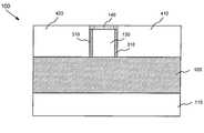
- FIG. 1illustrates the cross-section of a semiconductor device 100 formed in accordance with an embodiment of the present invention.
- semiconductor device 100may include a silicon on insulator (SOI) structure that includes a silicon substrate 110 , a buried oxide layer 120 and a silicon layer 130 on the buried oxide layer 120 . Buried oxide layer 120 and silicon layer 130 may be formed on substrate 110 in a conventional manner.
- SOIsilicon on insulator
- buried oxide layer 120may include a silicon oxide and may have a thickness ranging from about 1000 ⁇ to about 3000 ⁇ .
- Silicon layer 130may include monocrystalline or polycrystalline silicon having a thickness ranging from about 300 ⁇ to about 1500 ⁇ . Silicon layer 130 is used to form a fin structure for a double gate transistor device, as described in more detail below.
- substrate 110 and layer 130may include other semiconducting materials, such as germanium, or combinations of semiconducting materials, such as silicon-germanium.
- Buried oxide layer 120may also include other dielectric materials.
- a dielectric layer 140such as a silicon nitride layer or a silicon oxide layer (e.g., SiO 2 ), may be formed over silicon layer 130 to act as a protective cap during subsequent etching processes.
- dielectric layer 140may be deposited at a thickness ranging from about 150 ⁇ to about 600 ⁇ .
- a photoresist materialmay be deposited and patterned to form a photoresist mask 150 for subsequent processing.
- the photoresistmay be deposited and patterned in any conventional manner.
- Semiconductor device 100may then be etched and the photoresist mask 150 may be removed.
- silicon layer 130may be etched in a conventional manner, with the etching terminating on buried oxide layer 120 to form a fin.
- source and drain regionsmay be formed adjacent the respective ends of the fin.
- a layer of silicon, germanium or combination of silicon and germaniummay be deposited, patterned and etched in a conventional manner to form source and drain regions.
- FIG. 2Aschematically illustrates the top view of a fin structure on semiconductor 100 formed in such a manner.
- Source region 220 and drain region 230may be formed adjacent the ends of fin 210 on buried oxide layer 120 , according to an exemplary embodiment of the present invention.
- FIG. 2Bis a cross-section along line A-A′ in FIG. 2A illustrating the fin structure in accordance with an exemplary embodiment of the present invention.
- Dielectric layer 140 and silicon layer 130have been etched to form fin 210 .
- Fin 210may include silicon 130 and a dielectric cap 140 .
- FIG. 3is a cross-section illustrating the formation of a gate dielectric layer and gate material on fin 210 in accordance with an exemplary embodiment of the present invention.
- a dielectric layermay be formed on fin 210 .
- a thin oxide film 310may be thermally grown on fin 210 , as illustrated in FIG. 4 .
- the oxide film 310may be grown to a thickness of about 10 ⁇ to about 50 ⁇ and may be formed on the exposed side surfaces of silicon 130 in fin 210 to act as a dielectric layer for a subsequently formed gate electrode. Similar to the oxide film 310 , the dielectric cap 140 may provide electrical insulation for the top surface of fin 210 .
- a gate material layer 320may be deposited over semiconductor device 100 after formation of the oxide film 310 .
- the gate material layer 320may comprise the material for the subsequently formed gate electrode.
- the gate material layer 320may include polysilicon deposited using conventional chemical vapor deposition (CVD) to a thickness ranging from about 300 ⁇ to about 1500 ⁇ .
- CVDchemical vapor deposition
- other semiconducting materialssuch as germanium or combinations of silicon and germanium, or various metals may be used as the gate material.
- Gate material layer 320may be selectively etched to form a gate structure out of the gate material layer 320 on device 100 . Forming the gate structure in such a manner may leave some gate material 320 on top of the dielectric cap 140 , for example as illustrated in FIG. 3 .
- FIG. 4is a cross-section illustrating the planarizing of the gate material 320 in accordance with an exemplary embodiment of the present invention.
- Excess gate materialmay be removed (e.g., from above the dielectric cap 140 ) to planarize the fin region of the semiconductor device 100 .
- CMPchemical-mechanical polishing
- CMPmay be performed so that the gate material (i.e., layer 320 ) is even with or nearly even with dielectric cap 140 in the vertical direction, as illustrated in FIG. 4 .
- the gate material layer 320 in the channel region of semiconductor device 100abuts fin 210 on the two side surfaces to form a first gate 410 and a second gate 420 .
- the top surface of fin 210is covered by dielectric cap 140 .
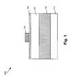
- FIG. 5illustrates a top view of semiconductor device 100 consistent with the present invention.
- first gate 410 and second gate 420are shown adjacent, but not covering, fin 210 .
- the gate material layer 320may then be patterned and etched to form two gate electrodes. As illustrated in FIG. 5, semiconductor device 100 includes a double gate structure with gate electrodes 510 and 520 . Gate electrodes 510 and 520 are effectively separated by fin 210 and may be separately biased, as discussed in more detail below.
- the gate dielectric 310(FIG. 4) surrounding the side surfaces of fin 210 is not shown in FIG. 5 for simplicity.
- the source/drain regions 220 and 230may then be doped.
- n-type or p-type impuritiesmay be implanted in source/drain regions 220 and 230 .
- the particular implantation dosages and energiesmay be selected based on the particular end device requirements.
- One or ordinary skill in this artwould be able to optimize the source/drain implantation process based on the circuit requirements and such steps are not disclosed herein in order not to unduly obscure the thrust of the present invention.
- sidewall spacers(not shown) may optionally be formed prior to the source/drain ion implantation to control the location of the source/drain junctions based on the particular circuit requirements.
- Activation annealingmay then be performed to activate the source/drain regions 220 and 230 .
- gate electrode 510 and gate electrode 520are physically and electrically separated from each other.
- each of the gate electrodes 510 and 520may be separately biased with different voltages when used in a circuit.
- the capability for independently biasing the gates 410 and 420 (via gate electrodes 510 and 520 )increases the flexibility of circuit design using semiconductor device 100 .
- the resulting semiconductor device 100 illustrated in FIG. 5is a double gate device with a first gate 410 and a second gate 420 .
- the gate material layer 320(FIGS. 3 and 4) abuts two surfaces of fin 210 and provides semiconductor device 100 with increased channel width per device, as compared to a conventional double gate device.
- the fin 210may also retain the dielectric cap 140 that protects the fin 210 during gate etching.
- the gates 410 and 420are also effectively separated by fin 210 and may be separately biased (via respective gate electrodes 510 and 520 ) based on the particular circuit requirements of device 100 .
- This separate double gate structureprovides increased flexibility during circuit design, as opposed to conventional FinFETs which include a single gat connection.
- a double-gate FinFET deviceis formed with two separate gates in the channel region of the device.
- the resulting structureexhibits good short channel behavior.
- the present inventionprovides increased flexibility and can be easily integrated into conventional processing.
- FIGS. 6A-6Dare cross-sections illustrating the induction of tensile strain in a fin in accordance with another implementation of the present invention.
- FIG. 6Aillustrates the cross-section of a semiconductor device 600 .
- device 600may include a buried oxide (BOX) layer 610 , a fin 620 , and an SiO 2 cap 630 .
- BOXburied oxide
- Elements 610 - 630may be formed as described above with respect to FIGS. 1-2B.
- Fin 620may include silicon, germanium or a combination of silicon and germanium.
- a thick sacrificial oxide layer 640may be thermally grown on fin 620 as shown in FIG. 6 B. Growing the thick (e.g., 200-400 ⁇ ) sacrificial oxide layer 640 may induce a tensile strain in fin 620 . The sacrificial oxide layer 640 may then be removed, and a thin gate oxide layer 650 may be grown, as illustrated in FIG. 6 C. Gate material 660 may then be deposited over the fin 620 as shown in FIG. 6D.
- a FinFETmay be formed from the structure in FIG. 6D in a typical manner. The fin 620 in such a FinFET will have a tensile strain, imparting qualities to the fin 620 that will be understood by those skilled in the art.
- FIGS. 7A and 7Bare views illustrating exemplary processing for forming a FinFET with a fully silicided gate.
- device 700includes a fin 710 , source region 720 , and drain region 730 . These layers/structures may be formed as described above with respect to FIGS. 1-2B.
- fin 710may include a top oxide cap 740 and gate oxide 750 surrounding a silicon structure. Fin 710 may be formed on a buried oxide (BOX) layer 705 .
- BOXburied oxide
- a thin polysilicon layer 760may be deposited on the fin 710 , as shown in FIG. 7 C. Then a thick bottom antireflective (BARC) layer 770 may be deposited, as shown in FIG. 7 D. The gate region and contacts 780 may then be patterned and etched as shown from the top in FIG. 7 E.
- BARCbottom antireflective
- Source and drain regions 720 and 730may be implanted with ions without removing the BARC layer 770 . Thus, the dopants used will be stopped by the BARC layer 770 from penetrating into the channel (e.g., fin 710 ).
- BARC layer 770may be removed, and the polysilicon 760 is fully silicided to form a metal gate 780 , as illustrated in FIGS. 7E and 7F.
- the gate material 710may also be planarized in a manner similar to that described above with respect to FIG. 4 .
- the dielectric and conductive layers used in manufacturing a semiconductor device in accordance with the present inventioncan be deposited by conventional deposition techniques.
- metallization techniquessuch as various types of CVD processes, including low pressure CVD (LPCVD) and enhanced CVD (ECVD) can be employed.
- LPCVDlow pressure CVD
- ECVDenhanced CVD
- the present inventionis applicable in the manufacturing of double-gate semiconductor devices and particularly in FinFET devices with design features of 100 nm and below.
- the present inventionis applicable to the formation of any of various types of semiconductor devices, and hence, details have not been set forth in order to avoid obscuring the thrust of the present invention.
- conventional photolithographic and etching techniquesare employed and, hence, the details of such techniques have not been set forth herein in detail.
Landscapes
- Thin Film Transistor (AREA)
- Insulated Gate Type Field-Effect Transistor (AREA)
- Testing Or Measuring Of Semiconductors Or The Like (AREA)
Abstract
Description
Claims (15)
Priority Applications (10)
| Application Number | Priority Date | Filing Date | Title |
|---|---|---|---|
| US10/290,158US6611029B1 (en) | 2002-11-08 | 2002-11-08 | Double gate semiconductor device having separate gates |
| US10/602,061US20040126975A1 (en) | 2002-11-08 | 2003-06-24 | Double gate semiconductor device having separate gates |
| CNB2003801027590ACN100459166C (en) | 2002-11-08 | 2003-10-14 | Double gate semiconductor device having separate gates |
| KR1020057008204AKR101029383B1 (en) | 2002-11-08 | 2003-10-14 | Double Gate Semiconductor Devices With Separate Gates |
| AU2003291641AAU2003291641A1 (en) | 2002-11-08 | 2003-10-14 | Double gate semiconductor device having separate gates |
| PCT/US2003/032662WO2004044992A1 (en) | 2002-11-08 | 2003-10-14 | Double gate semiconductor device having separate gates |
| JP2004551527AJP2006505950A (en) | 2002-11-08 | 2003-10-14 | Double-gate semiconductor device having multiple separated gates |
| GB0504833AGB2408849B (en) | 2002-11-08 | 2003-10-14 | Double gate semiconductor device having separate gates |
| DE10393687TDE10393687B4 (en) | 2002-11-08 | 2003-10-14 | Double gate semiconductor device with separate gates and method for producing the dual gate semiconductor device |
| TW092130612ATWI311371B (en) | 2002-11-08 | 2003-11-03 | Double gate semiconductor device having separate gates |
Applications Claiming Priority (1)
| Application Number | Priority Date | Filing Date | Title |
|---|---|---|---|
| US10/290,158US6611029B1 (en) | 2002-11-08 | 2002-11-08 | Double gate semiconductor device having separate gates |
Related Child Applications (1)
| Application Number | Title | Priority Date | Filing Date |
|---|---|---|---|
| US10/602,061DivisionUS20040126975A1 (en) | 2002-11-08 | 2003-06-24 | Double gate semiconductor device having separate gates |
Publications (1)
| Publication Number | Publication Date |
|---|---|
| US6611029B1true US6611029B1 (en) | 2003-08-26 |
Family
ID=27757499
Family Applications (2)
| Application Number | Title | Priority Date | Filing Date |
|---|---|---|---|
| US10/290,158Expired - LifetimeUS6611029B1 (en) | 2002-11-08 | 2002-11-08 | Double gate semiconductor device having separate gates |
| US10/602,061AbandonedUS20040126975A1 (en) | 2002-11-08 | 2003-06-24 | Double gate semiconductor device having separate gates |
Family Applications After (1)
| Application Number | Title | Priority Date | Filing Date |
|---|---|---|---|
| US10/602,061AbandonedUS20040126975A1 (en) | 2002-11-08 | 2003-06-24 | Double gate semiconductor device having separate gates |
Country Status (9)
| Country | Link |
|---|---|
| US (2) | US6611029B1 (en) |
| JP (1) | JP2006505950A (en) |
| KR (1) | KR101029383B1 (en) |
| CN (1) | CN100459166C (en) |
| AU (1) | AU2003291641A1 (en) |
| DE (1) | DE10393687B4 (en) |
| GB (1) | GB2408849B (en) |
| TW (1) | TWI311371B (en) |
| WO (1) | WO2004044992A1 (en) |
Cited By (97)
| Publication number | Priority date | Publication date | Assignee | Title |
|---|---|---|---|---|
| US20040036127A1 (en)* | 2002-08-23 | 2004-02-26 | Chau Robert S. | Tri-gate devices and methods of fabrication |
| US20040061178A1 (en)* | 2002-09-30 | 2004-04-01 | Advanced Micro Devices Inc. | Finfet having improved carrier mobility and method of its formation |
| US20040099903A1 (en)* | 2002-11-26 | 2004-05-27 | Taiwan Semiconductor Manufacturing Co., Ltd. | Strained-channel multiple-gate transistor |
| US6756643B1 (en)* | 2003-06-12 | 2004-06-29 | Advanced Micro Devices, Inc. | Dual silicon layer for chemical mechanical polishing planarization |
| US20040126975A1 (en)* | 2002-11-08 | 2004-07-01 | Ahmed Shibly S. | Double gate semiconductor device having separate gates |
| US20040142545A1 (en)* | 2003-01-17 | 2004-07-22 | Advanced Micro Devices, Inc. | Semiconductor with tensile strained substrate and method of making the same |
| US20040145019A1 (en)* | 2003-01-23 | 2004-07-29 | Srikanteswara Dakshina-Murthy | Strained channel finfet |
| US20040217433A1 (en)* | 2003-04-29 | 2004-11-04 | Yee-Chia Yeo | Doping of semiconductor fin devices |
| US6815268B1 (en)* | 2002-11-22 | 2004-11-09 | Advanced Micro Devices, Inc. | Method for forming a gate in a FinFET device |
| US20040266077A1 (en)* | 2003-06-27 | 2004-12-30 | Yee-Chia Yeo | Structure and method for forming the gate electrode in a multiple-gate transistor |
| US20040266083A1 (en)* | 2003-06-27 | 2004-12-30 | Hareland Scott A. | Nonplanar device with stress incorporation layer and method of fabrication |
| US20050023633A1 (en)* | 2003-08-01 | 2005-02-03 | Yee-Chia Yeo | Semiconductor-on-insulator SRAM configured using partially-depleted and fully-depleted transistors |
| US20050082522A1 (en)* | 2003-07-25 | 2005-04-21 | Yi-Chun Huang | Strained channel transistor formation |
| US20050121706A1 (en)* | 2003-02-20 | 2005-06-09 | Hao-Yu Chen | Semiconductor nano-rod devices |
| US20050127412A1 (en)* | 2000-07-07 | 2005-06-16 | International Business Machines Corporation | Self-aligned double gate mosfet with separate gates |
| US20050148137A1 (en)* | 2003-12-30 | 2005-07-07 | Brask Justin K. | Nonplanar transistors with metal gate electrodes |
| US20050191795A1 (en)* | 2004-03-01 | 2005-09-01 | Dureseti Chidambarrao | Method of manufacture of FinFET devices with T-shaped fins and devices manufactured thereby |
| US20050199948A1 (en)* | 2004-03-09 | 2005-09-15 | Lee Jong-Wook | Fin field effect transistors with epitaxial extension layers and methods of forming the same |
| US6951784B1 (en) | 2004-08-05 | 2005-10-04 | International Business Machines Corporation | Three-mask method of constructing the final hard mask used for etching the silicon fins for FinFETs |
| US20050218438A1 (en)* | 2004-03-31 | 2005-10-06 | Nick Lindert | Bulk non-planar transistor having strained enhanced mobility and methods of fabrication |
| US20050233565A1 (en)* | 2004-04-15 | 2005-10-20 | International Business Machines Corporation | Methods for manufacturing a finfet using a conventional wafer and apparatus manufactured therefrom |
| US20050237850A1 (en)* | 2003-10-02 | 2005-10-27 | Suman Datta | Method and apparatus for improving stability of a 6T CMOS SRAM cell |
| US20050239242A1 (en)* | 2004-04-23 | 2005-10-27 | International Business Machines Corporation | structure and method of manufacturing a finFet device having stacked fins |
| US20050272192A1 (en)* | 2004-06-04 | 2005-12-08 | Chang-Woo Oh | Methods of forming fin field effect transistors using oxidation barrier layers and related devices |
| US20050275010A1 (en)* | 2004-06-10 | 2005-12-15 | Hung-Wei Chen | Semiconductor nano-wire devices and methods of fabrication |
| US20050275040A1 (en)* | 2004-06-11 | 2005-12-15 | International Business Machines Corporation | Back gate finfet sram |
| US20060001109A1 (en)* | 2004-06-30 | 2006-01-05 | Shaheen Mohamad A | High mobility tri-gate devices and methods of fabrication |
| WO2006003104A1 (en)* | 2004-06-30 | 2006-01-12 | International Business Machines Corporation | Method and structure for strained finfet devices |
| US20060022268A1 (en)* | 2004-07-27 | 2006-02-02 | Chang-Woo Oh | Semiconductor devices including stress inducing layers |
| US20060033095A1 (en)* | 2004-08-10 | 2006-02-16 | Doyle Brian S | Non-planar pMOS structure with a strained channel region and an integrated strained CMOS flow |
| US20060063332A1 (en)* | 2004-09-23 | 2006-03-23 | Brian Doyle | U-gate transistors and methods of fabrication |
| US20060068550A1 (en)* | 2004-09-29 | 2006-03-30 | Intel Corporation | Independently accessed double-gate and tri-gate transistors in same process flow |
| US20060071275A1 (en)* | 2004-09-30 | 2006-04-06 | Brask Justin K | Nonplanar transistors with metal gate electrodes |
| US7029959B1 (en)* | 2003-05-06 | 2006-04-18 | Advanced Micro Devices, Inc. | Source and drain protection and stringer-free gate formation in semiconductor devices |
| US20060157794A1 (en)* | 2005-01-18 | 2006-07-20 | Doyle Brian S | Non-planar MOS structure with a strained channel region |
| US20060172497A1 (en)* | 2003-06-27 | 2006-08-03 | Hareland Scott A | Nonplanar semiconductor device with partially or fully wrapped around gate electrode and methods of fabrication |
| US20060177998A1 (en)* | 2003-09-03 | 2006-08-10 | Harrity & Snyder, L.L.P. | Fully silicided gate structure for finfet devices |
| US7091068B1 (en)* | 2002-12-06 | 2006-08-15 | Advanced Micro Devices, Inc. | Planarizing sacrificial oxide to improve gate critical dimension in semiconductor devices |
| US20060197147A1 (en)* | 2005-02-24 | 2006-09-07 | International Business Machines Corporation | Improved double gate isolation |
| US20060231929A1 (en)* | 2003-06-26 | 2006-10-19 | Anderson Brent A | Semiconductor device having freestanding semiconductor layer |
| US7148526B1 (en) | 2003-01-23 | 2006-12-12 | Advanced Micro Devices, Inc. | Germanium MOSFET devices and methods for making same |
| US20060286724A1 (en)* | 2005-06-21 | 2006-12-21 | International Business Machines Corporation | Substrate backgate for trigate fet |
| US20070001219A1 (en)* | 2005-06-30 | 2007-01-04 | Marko Radosavljevic | Block contact architectures for nanoscale channel transistors |
| US20070032973A1 (en)* | 2005-08-05 | 2007-02-08 | Semiconductor Manufacturing International (Shanghai) Corporation | Knowledge-based statistical method and system to determine reliability compatibility for semiconductor integrated circuits |
| US20070040223A1 (en)* | 2005-08-17 | 2007-02-22 | Intel Corporation | Lateral undercut of metal gate in SOI device |
| US20070090416A1 (en)* | 2005-09-28 | 2007-04-26 | Doyle Brian S | CMOS devices with a single work function gate electrode and method of fabrication |
| US20070122955A1 (en)* | 2005-11-29 | 2007-05-31 | International Business Machines Corporation | Method of manufacturing a semiconductor structure |
| US20070131983A1 (en)* | 2005-12-13 | 2007-06-14 | Intel Corporation | Tri-gate integration with embedded floating body memory cell using a high-K dual metal gate |
| US20070134878A1 (en)* | 2005-12-09 | 2007-06-14 | Intel Corporation | Non-planar microelectronic device having isolation element to mitigate fringe effects and method to fabricate same |
| US20070138514A1 (en)* | 2005-12-21 | 2007-06-21 | Chang Peter L | Integration of planar and tri-gate devices on the same substrate |
| US20070145483A1 (en)* | 2005-12-28 | 2007-06-28 | Kabushiki Kaisha Toshiba | Semiconductor device |
| US20070148926A1 (en)* | 2005-12-28 | 2007-06-28 | Intel Corporation | Dual halo implant for improving short channel effect in three-dimensional tri-gate transistors |
| US20070181930A1 (en)* | 2004-08-31 | 2007-08-09 | International Business Machines Corporation | Structure and method of making double-gated self-aligned finfet having gates of different lengths |
| US20070181947A1 (en)* | 2006-02-03 | 2007-08-09 | The Hong Kong University Of Science And Technology | Complementary metal-oxide-semiconductor transistor structure for high density and high performance integrated circuits |
| US7268058B2 (en) | 2004-01-16 | 2007-09-11 | Intel Corporation | Tri-gate transistors and methods to fabricate same |
| US20070232002A1 (en)* | 2006-03-29 | 2007-10-04 | Chang Peter L D | Static random access memory using independent double gate transistors |
| US20070231997A1 (en)* | 2006-03-31 | 2007-10-04 | Doyle Brian S | Stacked multi-gate transistor design and method of fabrication |
| US20070235763A1 (en)* | 2006-03-29 | 2007-10-11 | Doyle Brian S | Substrate band gap engineered multi-gate pMOS devices |
| US20070238273A1 (en)* | 2006-03-31 | 2007-10-11 | Doyle Brian S | Method of ion implanting for tri-gate devices |
| US20070264762A1 (en)* | 2003-11-04 | 2007-11-15 | Yee-Chia Yeo | Semiconductor-on-insulator SRAM configured using partially-depleted and fully-depleted transistors |
| US20080061316A1 (en)* | 2003-08-22 | 2008-03-13 | International Business Machines Corporation | Strained-channel fin field effect transistor (fet) with a uniform channel thickness and separate gates |
| US20080097346A1 (en)* | 2006-09-19 | 2008-04-24 | Alcon, Inc. | Trocar cannula |
| US20080099839A1 (en)* | 2006-06-14 | 2008-05-01 | Willy Rachmady | Ultra-thin oxide bonding for S1 to S1 dual orientation bonding |
| US20080121998A1 (en)* | 2006-09-15 | 2008-05-29 | Kavalieros Jack T | Apparatus and method for selectively recessing spacers on multi-gate devices |
| WO2007133775A3 (en)* | 2006-05-15 | 2008-05-29 | Univ Carnegie Mellon | Integrated circuit, device, system, and method of fabrication |
| US20080137051A1 (en)* | 2004-12-21 | 2008-06-12 | Carnegie Mellon University | Lithography and Associated Methods, Devices, and Systems |
| US7396711B2 (en) | 2005-12-27 | 2008-07-08 | Intel Corporation | Method of fabricating a multi-cornered film |
| US20080173942A1 (en)* | 2007-01-22 | 2008-07-24 | International Business Machines Corporation | STRUCTURE AND METHOD OF MANUFACTURING A STRAINED FinFET WITH STRESSED SILICIDE |
| US7425500B2 (en) | 2006-03-31 | 2008-09-16 | Intel Corporation | Uniform silicide metal on epitaxially grown source and drain regions of three-dimensional transistors |
| CN100424886C (en)* | 2004-10-29 | 2008-10-08 | 国际商业机器公司 | FinFET body contact structure and method of creating this structure |
| US7479421B2 (en) | 2005-09-28 | 2009-01-20 | Intel Corporation | Process for integrating planar and non-planar CMOS transistors on a bulk substrate and article made thereby |
| US7518196B2 (en) | 2005-02-23 | 2009-04-14 | Intel Corporation | Field effect transistor with narrow bandgap source and drain regions and method of fabrication |
| US7525160B2 (en) | 2005-12-27 | 2009-04-28 | Intel Corporation | Multigate device with recessed strain regions |
| US20090114209A1 (en)* | 2005-06-16 | 2009-05-07 | Vkr Holding A/S | Solar Collector and Mounting Bracket |
| US7547637B2 (en) | 2005-06-21 | 2009-06-16 | Intel Corporation | Methods for patterning a semiconductor film |
| US7550333B2 (en) | 2004-10-25 | 2009-06-23 | Intel Corporation | Nonplanar device with thinned lower body portion and method of fabrication |
| US7579280B2 (en) | 2004-06-01 | 2009-08-25 | Intel Corporation | Method of patterning a film |
| US20090242987A1 (en)* | 2006-02-13 | 2009-10-01 | Nxp B.V. | Double-gate semiconductor devices having gates with different work functions and methods of manufacture thereof |
| US20090256208A1 (en)* | 2008-04-11 | 2009-10-15 | Kabushiki Kaisha Toshiba | Semiconductor device and method of fabricating the same |
| US7700470B2 (en) | 2006-09-22 | 2010-04-20 | Intel Corporation | Selective anisotropic wet etching of workfunction metal for semiconductor devices |
| US20100155801A1 (en)* | 2008-12-22 | 2010-06-24 | Doyle Brian S | Integrated circuit, 1T-1C embedded memory cell containing same, and method of manufacturing 1T-1C memory cell for embedded memory application |
| US20100163945A1 (en)* | 2008-12-30 | 2010-07-01 | Kavalieros Jack T | Embedded memory cell and method of manufacturing same |
| US20100314684A1 (en)* | 2008-02-11 | 2010-12-16 | Nxp B.V. | Finfet with separate gates and method for fabricating a finfet with separate gates |
| US7858481B2 (en) | 2005-06-15 | 2010-12-28 | Intel Corporation | Method for fabricating transistor with thinned channel |
| US20110021010A1 (en)* | 2009-07-27 | 2011-01-27 | International Business Machines Corporation | Method for double pattern density |
| US7879675B2 (en) | 2005-03-14 | 2011-02-01 | Intel Corporation | Field effect transistor with metal source/drain regions |
| US7915167B2 (en) | 2004-09-29 | 2011-03-29 | Intel Corporation | Fabrication of channel wraparound gate structure for field-effect transistor |
| US7989280B2 (en) | 2005-11-30 | 2011-08-02 | Intel Corporation | Dielectric interface for group III-V semiconductor device |
| US8217450B1 (en) | 2004-02-03 | 2012-07-10 | GlobalFoundries, Inc. | Double-gate semiconductor device with gate contacts formed adjacent sidewalls of a fin |
| US8362566B2 (en) | 2008-06-23 | 2013-01-29 | Intel Corporation | Stress in trigate devices using complimentary gate fill materials |
| US8617945B2 (en) | 2006-08-02 | 2013-12-31 | Intel Corporation | Stacking fault and twin blocking barrier for integrating III-V on Si |
| US8785273B2 (en) | 2012-04-11 | 2014-07-22 | International Business Machines Corporation | FinFET non-volatile memory and method of fabrication |
| US9018713B2 (en) | 2012-06-25 | 2015-04-28 | International Business Machines Corporation | Plural differential pair employing FinFET structure |
| US9024387B2 (en) | 2012-06-25 | 2015-05-05 | International Business Machines Corporation | FinFET with body contact |
| US9577101B2 (en) | 2015-03-13 | 2017-02-21 | Taiwan Semiconductor Manufacturing Company, Ltd. | Source/drain regions for fin field effect transistors and methods of forming same |
| CN106898553A (en)* | 2017-03-16 | 2017-06-27 | 北京大学 | A kind of fin formula field effect transistor and preparation method thereof |
| CN106952959A (en)* | 2017-03-16 | 2017-07-14 | 北京大学 | A silicon germanium channel fin field effect transistor and its preparation method |
Families Citing this family (12)
| Publication number | Priority date | Publication date | Assignee | Title |
|---|---|---|---|---|
| US6913959B2 (en)* | 2003-06-23 | 2005-07-05 | Advanced Micro Devices, Inc. | Method of manufacturing a semiconductor device having a MESA structure |
| US7624192B2 (en)* | 2003-12-30 | 2009-11-24 | Microsoft Corporation | Framework for user interaction with multiple network devices |
| KR100541657B1 (en)* | 2004-06-29 | 2006-01-11 | 삼성전자주식회사 | Multi-gate transistor fabrication method and multi-gate transistor fabricated thereby |
| US7400031B2 (en)* | 2005-09-19 | 2008-07-15 | International Business Machines Corporation | Asymmetrically stressed CMOS FinFET |
| US7538391B2 (en)* | 2007-01-09 | 2009-05-26 | International Business Machines Corporation | Curved FINFETs |
| CN102479821B (en)* | 2010-11-30 | 2014-07-16 | 中国科学院微电子研究所 | Semiconductor device and method of forming the same |
| CN103022124B (en)* | 2011-09-22 | 2015-08-19 | 中芯国际集成电路制造(北京)有限公司 | Double-gated transistor and manufacture method thereof |
| US9059001B2 (en)* | 2011-12-16 | 2015-06-16 | Taiwan Semiconductor Manufacturing Company, Ltd. | Semiconductor device with biased feature |
| CN103811543B (en)* | 2012-11-05 | 2018-09-18 | 中国科学院微电子研究所 | Semiconductor device and method for manufacturing the same |
| CN105448688A (en)* | 2014-07-09 | 2016-03-30 | 中芯国际集成电路制造(上海)有限公司 | Gate formation method and semiconductor device |
| US9525072B2 (en) | 2014-08-11 | 2016-12-20 | Taiwan Semiconductor Manufacturing Company Limited | Semiconductor device and method of formation |
| CN105632936B (en)* | 2016-03-22 | 2018-10-16 | 上海华力微电子有限公司 | A kind of preparation method of bigrid fin formula field effect transistor |
Citations (3)
| Publication number | Priority date | Publication date | Assignee | Title |
|---|---|---|---|---|
| US5315143A (en)* | 1992-04-28 | 1994-05-24 | Matsushita Electric Industrial Co., Ltd. | High density integrated semiconductor device |
| US6396108B1 (en)* | 2000-11-13 | 2002-05-28 | Advanced Micro Devices, Inc. | Self-aligned double gate silicon-on-insulator (SOI) device |
| US6483171B1 (en)* | 1999-08-13 | 2002-11-19 | Micron Technology, Inc. | Vertical sub-micron CMOS transistors on (110), (111), (311), (511), and higher order surfaces of bulk, SOI and thin film structures and method of forming same |
Family Cites Families (27)
| Publication number | Priority date | Publication date | Assignee | Title |
|---|---|---|---|---|
| GB1601059A (en)* | 1978-05-31 | 1981-10-21 | Secr Defence | Fet devices and their fabrication |
| US5910912A (en)* | 1992-10-30 | 1999-06-08 | International Business Machines Corporation | Flash EEPROM with dual-sidewall gate |
| JP3252578B2 (en)* | 1993-12-27 | 2002-02-04 | ソニー株式会社 | Manufacturing method of planar insulated gate field effect transistor |
| US5757038A (en)* | 1995-11-06 | 1998-05-26 | International Business Machines Corporation | Self-aligned dual gate MOSFET with an ultranarrow channel |
| DE19846063A1 (en)* | 1998-10-07 | 2000-04-20 | Forschungszentrum Juelich Gmbh | Method of manufacturing a double-gate MOSFET |
| US6333247B1 (en)* | 1999-02-10 | 2001-12-25 | International Business Machines Corporation | Two-step MOSFET gate formation for high-density devices |
| US6159782A (en)* | 1999-08-05 | 2000-12-12 | Advanced Micro Devices, Inc. | Fabrication of field effect transistors having dual gates with gate dielectrics of high dielectric constant |
| US6252284B1 (en)* | 1999-12-09 | 2001-06-26 | International Business Machines Corporation | Planarized silicon fin device |
| KR100353551B1 (en)* | 2000-01-28 | 2002-09-27 | 주식회사 하이닉스반도체 | Method of forming silicide |
| JP4044276B2 (en)* | 2000-09-28 | 2008-02-06 | 株式会社東芝 | Semiconductor device and manufacturing method thereof |
| US6413802B1 (en)* | 2000-10-23 | 2002-07-02 | The Regents Of The University Of California | Finfet transistor structures having a double gate channel extending vertically from a substrate and methods of manufacture |
| US6472258B1 (en)* | 2000-11-13 | 2002-10-29 | International Business Machines Corporation | Double gate trench transistor |
| US6300182B1 (en)* | 2000-12-11 | 2001-10-09 | Advanced Micro Devices, Inc. | Field effect transistor having dual gates with asymmetrical doping for reduced threshold voltage |
| FR2822293B1 (en)* | 2001-03-13 | 2007-03-23 | Nat Inst Of Advanced Ind Scien | FIELD EFFECT TRANSISTOR AND DOUBLE GRID, INTEGRATED CIRCUIT COMPRISING THIS TRANSISTOR, AND METHOD OF MANUFACTURING THE SAME |
| JP3543117B2 (en)* | 2001-03-13 | 2004-07-14 | 独立行政法人産業技術総合研究所 | Double gate field effect transistor |
| US6458662B1 (en)* | 2001-04-04 | 2002-10-01 | Advanced Micro Devices, Inc. | Method of fabricating a semiconductor device having an asymmetrical dual-gate silicon-germanium (SiGe) channel MOSFET and a device thereby formed |
| US6689650B2 (en)* | 2001-09-27 | 2004-02-10 | International Business Machines Corporation | Fin field effect transistor with self-aligned gate |
| US6657259B2 (en)* | 2001-12-04 | 2003-12-02 | International Business Machines Corporation | Multiple-plane FinFET CMOS |
| US6610576B2 (en)* | 2001-12-13 | 2003-08-26 | International Business Machines Corporation | Method for forming asymmetric dual gate transistor |
| US20030151077A1 (en)* | 2002-02-13 | 2003-08-14 | Leo Mathew | Method of forming a vertical double gate semiconductor device and structure thereof |
| US6657252B2 (en)* | 2002-03-19 | 2003-12-02 | International Business Machines Corporation | FinFET CMOS with NVRAM capability |
| US6635909B2 (en)* | 2002-03-19 | 2003-10-21 | International Business Machines Corporation | Strained fin FETs structure and method |
| US6770516B2 (en)* | 2002-09-05 | 2004-08-03 | Taiwan Semiconductor Manufacturing Company | Method of forming an N channel and P channel FINFET device on the same semiconductor substrate |
| US6833588B2 (en)* | 2002-10-22 | 2004-12-21 | Advanced Micro Devices, Inc. | Semiconductor device having a U-shaped gate structure |
| US6611029B1 (en)* | 2002-11-08 | 2003-08-26 | Advanced Micro Devices, Inc. | Double gate semiconductor device having separate gates |
| US7214991B2 (en)* | 2002-12-06 | 2007-05-08 | Taiwan Semiconductor Manufacturing Co., Ltd. | CMOS inverters configured using multiple-gate transistors |
| US6812119B1 (en)* | 2003-07-08 | 2004-11-02 | Advanced Micro Devices, Inc. | Narrow fins by oxidation in double-gate finfet |
- 2002
- 2002-11-08USUS10/290,158patent/US6611029B1/ennot_activeExpired - Lifetime
- 2003
- 2003-06-24USUS10/602,061patent/US20040126975A1/ennot_activeAbandoned
- 2003-10-14CNCNB2003801027590Apatent/CN100459166C/ennot_activeExpired - Lifetime
- 2003-10-14DEDE10393687Tpatent/DE10393687B4/ennot_activeExpired - Lifetime
- 2003-10-14KRKR1020057008204Apatent/KR101029383B1/ennot_activeExpired - Lifetime
- 2003-10-14WOPCT/US2003/032662patent/WO2004044992A1/enactiveApplication Filing
- 2003-10-14AUAU2003291641Apatent/AU2003291641A1/ennot_activeAbandoned
- 2003-10-14JPJP2004551527Apatent/JP2006505950A/enactivePending
- 2003-10-14GBGB0504833Apatent/GB2408849B/ennot_activeExpired - Lifetime
- 2003-11-03TWTW092130612Apatent/TWI311371B/ennot_activeIP Right Cessation
Patent Citations (3)
| Publication number | Priority date | Publication date | Assignee | Title |
|---|---|---|---|---|
| US5315143A (en)* | 1992-04-28 | 1994-05-24 | Matsushita Electric Industrial Co., Ltd. | High density integrated semiconductor device |
| US6483171B1 (en)* | 1999-08-13 | 2002-11-19 | Micron Technology, Inc. | Vertical sub-micron CMOS transistors on (110), (111), (311), (511), and higher order surfaces of bulk, SOI and thin film structures and method of forming same |
| US6396108B1 (en)* | 2000-11-13 | 2002-05-28 | Advanced Micro Devices, Inc. | Self-aligned double gate silicon-on-insulator (SOI) device |
Non-Patent Citations (7)
| Title |
|---|
| Digh Hisamoto et al., "FinFET-A Self-Aligned Double-Gate MOSFET Scalable to 20 nm," IEEE Transactions on Electron Devices, vol. 47, No. 12, Dec. 2000, pp. 2320-2325. |
| U.S. application Ser. No. 10/290,330, filed Nov. 8, 2002, entitled "Double-Gate Semiconductor Device," Bin Yu et al., 20 page specification, 11 sheets of drawings. |
| U.S. application Ser. No. 10/348,758, filed Jan. 23, 2003, entitled "Germanium MOSFET Devices and Methods for Making Same," Judy Xilin An et al., 22 page specification, 29 sheets of drawings. |
| Xuejue Huang et al., "Sub 50-nm FinFET: PMOS," 1999 IEEE, IEDM, pp. 67-70. |
| Xuejue Huang et al., "Sub-50 nm P-Channel FinFET," IEEE Transactions on Electron Devices, vol. 48, No. 5, May 2001, pp. 880-886. |
| Yang-Kyu Choi et al., "Nanoscale CMOS Spacer FinFET for the Terabit Era," IEEE Electron Device Letters, vol. 23, No. 1, Jan. 2002, pp. 25-27. |
| Yang-Kyu Choi et al., "Sub-20nm CMOS FinFET Technologies," 2001 IEEE, IEDM, pp. 421-424. |
Cited By (264)
| Publication number | Priority date | Publication date | Assignee | Title |
|---|---|---|---|---|
| US20050127412A1 (en)* | 2000-07-07 | 2005-06-16 | International Business Machines Corporation | Self-aligned double gate mosfet with separate gates |
| US7101762B2 (en)* | 2000-07-07 | 2006-09-05 | International Business Machines Corporation | Self-aligned double gate mosfet with separate gates |
| US7358121B2 (en) | 2002-08-23 | 2008-04-15 | Intel Corporation | Tri-gate devices and methods of fabrication |
| US20040036127A1 (en)* | 2002-08-23 | 2004-02-26 | Chau Robert S. | Tri-gate devices and methods of fabrication |
| US7504678B2 (en) | 2002-08-23 | 2009-03-17 | Intel Corporation | Tri-gate devices and methods of fabrication |
| US7514346B2 (en) | 2002-08-23 | 2009-04-07 | Intel Corporation | Tri-gate devices and methods of fabrication |
| US20050199950A1 (en)* | 2002-08-23 | 2005-09-15 | Chau Robert S. | Tri-gate devices and methods of fabrication |
| US20040094807A1 (en)* | 2002-08-23 | 2004-05-20 | Chau Robert S. | Tri-gate devices and methods of fabrication |
| US7368791B2 (en) | 2002-08-23 | 2008-05-06 | Intel Corporation | Multi-gate carbon nano-tube transistors |
| US20070034972A1 (en)* | 2002-08-23 | 2007-02-15 | Chau Robert S | Tri-gate devices and methods of fabrication |
| US7427794B2 (en) | 2002-08-23 | 2008-09-23 | Intel Corporation | Tri-gate devices and methods of fabrication |
| US6858478B2 (en)* | 2002-08-23 | 2005-02-22 | Intel Corporation | Tri-gate devices and methods of fabrication |
| US7560756B2 (en) | 2002-08-23 | 2009-07-14 | Intel Corporation | Tri-gate devices and methods of fabrication |
| US20040036126A1 (en)* | 2002-08-23 | 2004-02-26 | Chau Robert S. | Tri-gate devices and methods of fabrication |
| US20060228840A1 (en)* | 2002-08-23 | 2006-10-12 | Chau Robert S | Tri-gate devices and methods of fabrication |
| US20040061178A1 (en)* | 2002-09-30 | 2004-04-01 | Advanced Micro Devices Inc. | Finfet having improved carrier mobility and method of its formation |
| US6800910B2 (en)* | 2002-09-30 | 2004-10-05 | Advanced Micro Devices, Inc. | FinFET device incorporating strained silicon in the channel region |
| US20040126975A1 (en)* | 2002-11-08 | 2004-07-01 | Ahmed Shibly S. | Double gate semiconductor device having separate gates |
| US6815268B1 (en)* | 2002-11-22 | 2004-11-09 | Advanced Micro Devices, Inc. | Method for forming a gate in a FinFET device |
| US6855990B2 (en)* | 2002-11-26 | 2005-02-15 | Taiwan Semiconductor Manufacturing Co., Ltd | Strained-channel multiple-gate transistor |
| US20040099903A1 (en)* | 2002-11-26 | 2004-05-27 | Taiwan Semiconductor Manufacturing Co., Ltd. | Strained-channel multiple-gate transistor |
| US7091068B1 (en)* | 2002-12-06 | 2006-08-15 | Advanced Micro Devices, Inc. | Planarizing sacrificial oxide to improve gate critical dimension in semiconductor devices |
| US7701019B2 (en) | 2003-01-17 | 2010-04-20 | Advanced Micro Devices, Inc. | Tensile strained substrate |
| US20060138479A1 (en)* | 2003-01-17 | 2006-06-29 | Advanced Micro Devices, Inc. | Tensile strained substrate |
| US7001837B2 (en)* | 2003-01-17 | 2006-02-21 | Advanced Micro Devices, Inc. | Semiconductor with tensile strained substrate and method of making the same |
| US20040142545A1 (en)* | 2003-01-17 | 2004-07-22 | Advanced Micro Devices, Inc. | Semiconductor with tensile strained substrate and method of making the same |
| US20040195627A1 (en)* | 2003-01-23 | 2004-10-07 | Srikanteswara Dakshina-Murthy | Strained channel FinFET |
| US6897527B2 (en) | 2003-01-23 | 2005-05-24 | Advanced Micro Devices, Inc. | Strained channel FinFET |
| US7781810B1 (en) | 2003-01-23 | 2010-08-24 | Advanced Micro Devices, Inc. | Germanium MOSFET devices and methods for making same |
| US7148526B1 (en) | 2003-01-23 | 2006-12-12 | Advanced Micro Devices, Inc. | Germanium MOSFET devices and methods for making same |
| US6803631B2 (en)* | 2003-01-23 | 2004-10-12 | Advanced Micro Devices, Inc. | Strained channel finfet |
| US8334181B1 (en) | 2003-01-23 | 2012-12-18 | Advanced Micro Devices, Inc. | Germanium MOSFET devices and methods for making same |
| US20040145019A1 (en)* | 2003-01-23 | 2004-07-29 | Srikanteswara Dakshina-Murthy | Strained channel finfet |
| US20050121706A1 (en)* | 2003-02-20 | 2005-06-09 | Hao-Yu Chen | Semiconductor nano-rod devices |
| US20040217433A1 (en)* | 2003-04-29 | 2004-11-04 | Yee-Chia Yeo | Doping of semiconductor fin devices |
| US8790970B2 (en) | 2003-04-29 | 2014-07-29 | Taiwan Semiconductor Manufacturing Company, Ltd. | Doping of semiconductor fin devices |
| US7074656B2 (en) | 2003-04-29 | 2006-07-11 | Taiwan Semiconductor Manufacturing Company, Ltd. | Doping of semiconductor fin devices |
| US7701008B2 (en) | 2003-04-29 | 2010-04-20 | Taiwan Semiconductor Manufacturing Company, Ltd. | Doping of semiconductor fin devices |
| US20060220133A1 (en)* | 2003-04-29 | 2006-10-05 | Yee-Chia Yeo | Doping of semiconductor fin devices |
| US20060234431A1 (en)* | 2003-04-29 | 2006-10-19 | Yee-Chia Yeo | Doping of semiconductor fin devices |
| US8053839B2 (en) | 2003-04-29 | 2011-11-08 | Taiwan Semiconductor Manufacturing Company, Ltd. | Doping of semiconductor fin devices |
| US20100176424A1 (en)* | 2003-04-29 | 2010-07-15 | Taiwan Semiconductor Manufacturing Company, Ltd. | Doping of Semiconductor Fin Devices |
| US7029959B1 (en)* | 2003-05-06 | 2006-04-18 | Advanced Micro Devices, Inc. | Source and drain protection and stringer-free gate formation in semiconductor devices |
| US20050056845A1 (en)* | 2003-06-12 | 2005-03-17 | Krishnashree Achuthan | Dual silicon layer for chemical mechanical polishing planarization |
| US6982464B2 (en) | 2003-06-12 | 2006-01-03 | Advanced Micro Devices, Inc. | Dual silicon layer for chemical mechanical polishing planarization |
| US6812076B1 (en) | 2003-06-12 | 2004-11-02 | Advanced Micro Devices, Inc. | Dual silicon layer for chemical mechanical polishing planarization |
| US6756643B1 (en)* | 2003-06-12 | 2004-06-29 | Advanced Micro Devices, Inc. | Dual silicon layer for chemical mechanical polishing planarization |
| US7709892B2 (en)* | 2003-06-26 | 2010-05-04 | International Business Machines Corporation | Semiconductor device having freestanding semiconductor layer |
| US20060231929A1 (en)* | 2003-06-26 | 2006-10-19 | Anderson Brent A | Semiconductor device having freestanding semiconductor layer |
| US7714397B2 (en) | 2003-06-27 | 2010-05-11 | Intel Corporation | Tri-gate transistor device with stress incorporation layer and method of fabrication |
| US20040266083A1 (en)* | 2003-06-27 | 2004-12-30 | Hareland Scott A. | Nonplanar device with stress incorporation layer and method of fabrication |
| US8405164B2 (en) | 2003-06-27 | 2013-03-26 | Intel Corporation | Tri-gate transistor device with stress incorporation layer and method of fabrication |
| US8273626B2 (en) | 2003-06-27 | 2012-09-25 | Intel Corporationn | Nonplanar semiconductor device with partially or fully wrapped around gate electrode and methods of fabrication |
| US20060091428A1 (en)* | 2003-06-27 | 2006-05-04 | Yee-Chia Yeo | Structure and method for forming the gate electrode in a multiple-gate transistor |
| US7005330B2 (en) | 2003-06-27 | 2006-02-28 | Taiwan Semiconductor Manufacturing Company, Ltd. | Structure and method for forming the gate electrode in a multiple-gate transistor |
| US7241653B2 (en) | 2003-06-27 | 2007-07-10 | Intel Corporation | Nonplanar device with stress incorporation layer and method of fabrication |
| US20050242406A1 (en)* | 2003-06-27 | 2005-11-03 | Hareland Scott A | Nonplanar device with stress incorporation layer and method of fabrication |
| US20040266077A1 (en)* | 2003-06-27 | 2004-12-30 | Yee-Chia Yeo | Structure and method for forming the gate electrode in a multiple-gate transistor |
| US7456476B2 (en) | 2003-06-27 | 2008-11-25 | Intel Corporation | Nonplanar semiconductor device with partially or fully wrapped around gate electrode and methods of fabrication |
| US20060172497A1 (en)* | 2003-06-27 | 2006-08-03 | Hareland Scott A | Nonplanar semiconductor device with partially or fully wrapped around gate electrode and methods of fabrication |
| US7276763B2 (en) | 2003-06-27 | 2007-10-02 | Taiwan Semiconductor Manufacturing Company, Ltd. | Structure and method for forming the gate electrode in a multiple-gate transistor |
| US7820513B2 (en) | 2003-06-27 | 2010-10-26 | Intel Corporation | Nonplanar semiconductor device with partially or fully wrapped around gate electrode and methods of fabrication |
| US7867860B2 (en) | 2003-07-25 | 2011-01-11 | Taiwan Semiconductor Manufacturing Company, Ltd. | Strained channel transistor formation |
| US20050082522A1 (en)* | 2003-07-25 | 2005-04-21 | Yi-Chun Huang | Strained channel transistor formation |
| US20050023633A1 (en)* | 2003-08-01 | 2005-02-03 | Yee-Chia Yeo | Semiconductor-on-insulator SRAM configured using partially-depleted and fully-depleted transistors |
| US7301206B2 (en) | 2003-08-01 | 2007-11-27 | Taiwan Semiconductor Manufacturing Company, Ltd. | Semiconductor-on-insulator SRAM configured using partially-depleted and fully-depleted transistors |
| US7842562B2 (en) | 2003-08-22 | 2010-11-30 | International Business Machines Corporation | Strained-channel fin field effect transistor (FET) with a uniform channel thickness and separate gates |
| US7915685B2 (en) | 2003-08-22 | 2011-03-29 | International Business Machines Corporation | Strained-channel fin field effect transistor (FET) with a uniform channel thickness and separate gates |
| US20080061316A1 (en)* | 2003-08-22 | 2008-03-13 | International Business Machines Corporation | Strained-channel fin field effect transistor (fet) with a uniform channel thickness and separate gates |
| US20060177998A1 (en)* | 2003-09-03 | 2006-08-10 | Harrity & Snyder, L.L.P. | Fully silicided gate structure for finfet devices |
| US8008136B2 (en)* | 2003-09-03 | 2011-08-30 | Advanced Micro Devices, Inc. | Fully silicided gate structure for FinFET devices |
| US20050237850A1 (en)* | 2003-10-02 | 2005-10-27 | Suman Datta | Method and apparatus for improving stability of a 6T CMOS SRAM cell |
| US7445980B2 (en) | 2003-10-02 | 2008-11-04 | Intel Corporation | Method and apparatus for improving stability of a 6T CMOS SRAM cell |
| US20060281236A1 (en)* | 2003-10-02 | 2006-12-14 | Suman Datta | Method and apparatus for improving stability of a 6T CMOS SRAM cell |
| US20070264762A1 (en)* | 2003-11-04 | 2007-11-15 | Yee-Chia Yeo | Semiconductor-on-insulator SRAM configured using partially-depleted and fully-depleted transistors |
| US7888201B2 (en) | 2003-11-04 | 2011-02-15 | Taiwan Semiconductor Manufacturing Company, Ltd. | Semiconductor-on-insulator SRAM configured using partially-depleted and fully-depleted transistors |
| US7105390B2 (en) | 2003-12-30 | 2006-09-12 | Intel Corporation | Nonplanar transistors with metal gate electrodes |
| US7329913B2 (en) | 2003-12-30 | 2008-02-12 | Intel Corporation | Nonplanar transistors with metal gate electrodes |
| US20050148137A1 (en)* | 2003-12-30 | 2005-07-07 | Brask Justin K. | Nonplanar transistors with metal gate electrodes |
| US20050156171A1 (en)* | 2003-12-30 | 2005-07-21 | Brask Justin K. | Nonplanar transistors with metal gate electrodes |
| US7268058B2 (en) | 2004-01-16 | 2007-09-11 | Intel Corporation | Tri-gate transistors and methods to fabricate same |
| US8217450B1 (en) | 2004-02-03 | 2012-07-10 | GlobalFoundries, Inc. | Double-gate semiconductor device with gate contacts formed adjacent sidewalls of a fin |
| US20050191795A1 (en)* | 2004-03-01 | 2005-09-01 | Dureseti Chidambarrao | Method of manufacture of FinFET devices with T-shaped fins and devices manufactured thereby |
| US7060539B2 (en) | 2004-03-01 | 2006-06-13 | International Business Machines Corporation | Method of manufacture of FinFET devices with T-shaped fins and devices manufactured thereby |
| US20050199948A1 (en)* | 2004-03-09 | 2005-09-15 | Lee Jong-Wook | Fin field effect transistors with epitaxial extension layers and methods of forming the same |
| US20050218438A1 (en)* | 2004-03-31 | 2005-10-06 | Nick Lindert | Bulk non-planar transistor having strained enhanced mobility and methods of fabrication |
| US20050224800A1 (en)* | 2004-03-31 | 2005-10-13 | Nick Lindert | Bulk non-planar transistor having strained enhanced mobility and methods of fabrication |
| US7781771B2 (en) | 2004-03-31 | 2010-08-24 | Intel Corporation | Bulk non-planar transistor having strained enhanced mobility and methods of fabrication |
| US7154118B2 (en) | 2004-03-31 | 2006-12-26 | Intel Corporation | Bulk non-planar transistor having strained enhanced mobility and methods of fabrication |
| US7326634B2 (en) | 2004-03-31 | 2008-02-05 | Intel Corporation | Bulk non-planar transistor having strained enhanced mobility and methods of fabrication |
| US7800152B2 (en) | 2004-04-15 | 2010-09-21 | International Business Machines Corporation | Methods for manufacturing a finfet using a conventional wafer and apparatus manufactured therefrom |
| US20050233565A1 (en)* | 2004-04-15 | 2005-10-20 | International Business Machines Corporation | Methods for manufacturing a finfet using a conventional wafer and apparatus manufactured therefrom |
| US7262084B2 (en) | 2004-04-15 | 2007-08-28 | International Business Machines Corporation | Methods for manufacturing a finFET using a conventional wafer and apparatus manufactured therefrom |
| US7098477B2 (en) | 2004-04-23 | 2006-08-29 | International Business Machines Corporation | Structure and method of manufacturing a finFET device having stacked fins |
| US20050239242A1 (en)* | 2004-04-23 | 2005-10-27 | International Business Machines Corporation | structure and method of manufacturing a finFet device having stacked fins |
| US7579280B2 (en) | 2004-06-01 | 2009-08-25 | Intel Corporation | Method of patterning a film |
| US7745871B2 (en) | 2004-06-04 | 2010-06-29 | Chang-Woo Oh | Fin field effect transistors including oxidation barrier layers |
| US20080029828A1 (en)* | 2004-06-04 | 2008-02-07 | Samsung Electronics Co., Ltd. | Fin field effect transistors including oxidation barrier layers |
| US7297600B2 (en) | 2004-06-04 | 2007-11-20 | Samsung Electronics Co., Ltd. | Methods of forming fin field effect transistors using oxidation barrier layers |
| US20050272192A1 (en)* | 2004-06-04 | 2005-12-08 | Chang-Woo Oh | Methods of forming fin field effect transistors using oxidation barrier layers and related devices |
| US7452778B2 (en) | 2004-06-10 | 2008-11-18 | Taiwan Semiconductor Manufacturing Company, Ltd. | Semiconductor nano-wire devices and methods of fabrication |
| US20050275010A1 (en)* | 2004-06-10 | 2005-12-15 | Hung-Wei Chen | Semiconductor nano-wire devices and methods of fabrication |
| US7084461B2 (en) | 2004-06-11 | 2006-08-01 | International Business Machines Corporation | Back gate FinFET SRAM |
| US20050275040A1 (en)* | 2004-06-11 | 2005-12-15 | International Business Machines Corporation | Back gate finfet sram |
| US20060183289A1 (en)* | 2004-06-11 | 2006-08-17 | Anderson Brent A | Back gate FinFET SRAM |
| US7491589B2 (en) | 2004-06-11 | 2009-02-17 | International Business Machines Corporation | Back gate FinFET SRAM |
| US20100065888A1 (en)* | 2004-06-30 | 2010-03-18 | Shaheen Mohamad A | High mobility tri-gate devices and methods of fabrication |
| US8084818B2 (en) | 2004-06-30 | 2011-12-27 | Intel Corporation | High mobility tri-gate devices and methods of fabrication |
| US20060001109A1 (en)* | 2004-06-30 | 2006-01-05 | Shaheen Mohamad A | High mobility tri-gate devices and methods of fabrication |
| WO2006003104A1 (en)* | 2004-06-30 | 2006-01-12 | International Business Machines Corporation | Method and structure for strained finfet devices |
| US20060014338A1 (en)* | 2004-06-30 | 2006-01-19 | International Business Machines Corporation | Method and structure for strained finfet devices |
| US8669145B2 (en) | 2004-06-30 | 2014-03-11 | International Business Machines Corporation | Method and structure for strained FinFET devices |
| US7042009B2 (en) | 2004-06-30 | 2006-05-09 | Intel Corporation | High mobility tri-gate devices and methods of fabrication |
| US20060022268A1 (en)* | 2004-07-27 | 2006-02-02 | Chang-Woo Oh | Semiconductor devices including stress inducing layers |
| US20110079859A1 (en)* | 2004-07-27 | 2011-04-07 | Chang-Woo Oh | Semiconductor devices including fin shaped semiconductor regions and stress inducing layers |
| US8461653B2 (en) | 2004-07-27 | 2013-06-11 | Samsung Electronics Co., Ltd. | Semiconductor devices including fin shaped semiconductor regions and stress inducing layers |
| US7859064B1 (en) | 2004-07-27 | 2010-12-28 | Samsung Electronics Co., Ltd. | Semiconductor devices including channel and junction regions of different semiconductor materials |
| US7271456B2 (en) | 2004-07-27 | 2007-09-18 | Samsung Electronics Co., Ltd. | Semiconductor devices including stress inducing layers |
| US7952151B2 (en) | 2004-07-27 | 2011-05-31 | Samsung Electronics Co., Ltd. | Semiconductor devices including fin shaped semiconductor regions and stress inducing layers |
| US6951784B1 (en) | 2004-08-05 | 2005-10-04 | International Business Machines Corporation | Three-mask method of constructing the final hard mask used for etching the silicon fins for FinFETs |
| US7348284B2 (en) | 2004-08-10 | 2008-03-25 | Intel Corporation | Non-planar pMOS structure with a strained channel region and an integrated strained CMOS flow |
| US20060033095A1 (en)* | 2004-08-10 | 2006-02-16 | Doyle Brian S | Non-planar pMOS structure with a strained channel region and an integrated strained CMOS flow |
| US7960794B2 (en) | 2004-08-10 | 2011-06-14 | Intel Corporation | Non-planar pMOS structure with a strained channel region and an integrated strained CMOS flow |
| US7785944B2 (en) | 2004-08-31 | 2010-08-31 | International Business Machines Corporation | Method of making double-gated self-aligned finFET having gates of different lengths |
| US7348641B2 (en) | 2004-08-31 | 2008-03-25 | International Business Machines Corporation | Structure and method of making double-gated self-aligned finFET having gates of different lengths |
| US20070181930A1 (en)* | 2004-08-31 | 2007-08-09 | International Business Machines Corporation | Structure and method of making double-gated self-aligned finfet having gates of different lengths |
| US20080176365A1 (en)* | 2004-08-31 | 2008-07-24 | Huilong Zhu | Method of making double-gated self-aligned finFET having gates of different lengths |
| US20060063332A1 (en)* | 2004-09-23 | 2006-03-23 | Brian Doyle | U-gate transistors and methods of fabrication |
| US7915167B2 (en) | 2004-09-29 | 2011-03-29 | Intel Corporation | Fabrication of channel wraparound gate structure for field-effect transistor |
| US7037790B2 (en) | 2004-09-29 | 2006-05-02 | Intel Corporation | Independently accessed double-gate and tri-gate transistors in same process flow |
| US7859053B2 (en) | 2004-09-29 | 2010-12-28 | Intel Corporation | Independently accessed double-gate and tri-gate transistors in same process flow |
| US20060128131A1 (en)* | 2004-09-29 | 2006-06-15 | Chang Peter L | Independently accessed double-gate and tri-gate transistors in same process flow |
| US20060068550A1 (en)* | 2004-09-29 | 2006-03-30 | Intel Corporation | Independently accessed double-gate and tri-gate transistors in same process flow |
| US8399922B2 (en) | 2004-09-29 | 2013-03-19 | Intel Corporation | Independently accessed double-gate and tri-gate transistors |
| US8268709B2 (en) | 2004-09-29 | 2012-09-18 | Intel Corporation | Independently accessed double-gate and tri-gate transistors in same process flow |
| US7326656B2 (en) | 2004-09-30 | 2008-02-05 | Intel Corporation | Method of forming a metal oxide dielectric |
| US7361958B2 (en) | 2004-09-30 | 2008-04-22 | Intel Corporation | Nonplanar transistors with metal gate electrodes |
| US7528025B2 (en) | 2004-09-30 | 2009-05-05 | Intel Corporation | Nonplanar transistors with metal gate electrodes |
| US20060071275A1 (en)* | 2004-09-30 | 2006-04-06 | Brask Justin K | Nonplanar transistors with metal gate electrodes |
| US20060138552A1 (en)* | 2004-09-30 | 2006-06-29 | Brask Justin K | Nonplanar transistors with metal gate electrodes |
| US20060138553A1 (en)* | 2004-09-30 | 2006-06-29 | Brask Justin K | Nonplanar transistors with metal gate electrodes |
| US7531437B2 (en) | 2004-09-30 | 2009-05-12 | Intel Corporation | Method of forming metal gate electrodes using sacrificial gate electrode material and sacrificial gate dielectric material |
| US8749026B2 (en) | 2004-10-25 | 2014-06-10 | Intel Corporation | Nonplanar device with thinned lower body portion and method of fabrication |
| US8502351B2 (en) | 2004-10-25 | 2013-08-06 | Intel Corporation | Nonplanar device with thinned lower body portion and method of fabrication |
| US8067818B2 (en) | 2004-10-25 | 2011-11-29 | Intel Corporation | Nonplanar device with thinned lower body portion and method of fabrication |
| US9190518B2 (en) | 2004-10-25 | 2015-11-17 | Intel Corporation | Nonplanar device with thinned lower body portion and method of fabrication |
| US9741809B2 (en) | 2004-10-25 | 2017-08-22 | Intel Corporation | Nonplanar device with thinned lower body portion and method of fabrication |
| US10236356B2 (en) | 2004-10-25 | 2019-03-19 | Intel Corporation | Nonplanar device with thinned lower body portion and method of fabrication |
| US7550333B2 (en) | 2004-10-25 | 2009-06-23 | Intel Corporation | Nonplanar device with thinned lower body portion and method of fabrication |
| CN100424886C (en)* | 2004-10-29 | 2008-10-08 | 国际商业机器公司 | FinFET body contact structure and method of creating this structure |
| US8259286B2 (en) | 2004-12-21 | 2012-09-04 | Carnegie Mellon University | Lithography and associated methods, devices, and systems |
| US20080137051A1 (en)* | 2004-12-21 | 2008-06-12 | Carnegie Mellon University | Lithography and Associated Methods, Devices, and Systems |
| US7531393B2 (en) | 2005-01-18 | 2009-05-12 | Intel Corporation | Non-planar MOS structure with a strained channel region |
| US20060157687A1 (en)* | 2005-01-18 | 2006-07-20 | Doyle Brian S | Non-planar MOS structure with a strained channel region |
| US20060157794A1 (en)* | 2005-01-18 | 2006-07-20 | Doyle Brian S | Non-planar MOS structure with a strained channel region |
| US7193279B2 (en) | 2005-01-18 | 2007-03-20 | Intel Corporation | Non-planar MOS structure with a strained channel region |
| US9368583B2 (en) | 2005-02-23 | 2016-06-14 | Intel Corporation | Field effect transistor with narrow bandgap source and drain regions and method of fabrication |
| US7518196B2 (en) | 2005-02-23 | 2009-04-14 | Intel Corporation | Field effect transistor with narrow bandgap source and drain regions and method of fabrication |
| US8368135B2 (en) | 2005-02-23 | 2013-02-05 | Intel Corporation | Field effect transistor with narrow bandgap source and drain regions and method of fabrication |
| US8183646B2 (en) | 2005-02-23 | 2012-05-22 | Intel Corporation | Field effect transistor with narrow bandgap source and drain regions and method of fabrication |
| US8664694B2 (en) | 2005-02-23 | 2014-03-04 | Intel Corporation | Field effect transistor with narrow bandgap source and drain regions and method of fabrication |
| US8816394B2 (en) | 2005-02-23 | 2014-08-26 | Intel Corporation | Field effect transistor with narrow bandgap source and drain regions and method of fabrication |
| US9048314B2 (en) | 2005-02-23 | 2015-06-02 | Intel Corporation | Field effect transistor with narrow bandgap source and drain regions and method of fabrication |
| US20100295129A1 (en)* | 2005-02-23 | 2010-11-25 | Chau Robert S | Field effect transistor with narrow bandgap source and drain regions and method of fabrication |
| US7825481B2 (en) | 2005-02-23 | 2010-11-02 | Intel Corporation | Field effect transistor with narrow bandgap source and drain regions and method of fabrication |
| US7893506B2 (en) | 2005-02-23 | 2011-02-22 | Intel Corporation | Field effect transistor with narrow bandgap source and drain regions and method of fabrication |
| US7537985B2 (en) | 2005-02-24 | 2009-05-26 | International Business Machines Corporation | Double gate isolation |
| US20060197147A1 (en)* | 2005-02-24 | 2006-09-07 | International Business Machines Corporation | Improved double gate isolation |
| US7288805B2 (en) | 2005-02-24 | 2007-10-30 | International Business Machines Corporation | Double gate isolation |
| US20070269950A1 (en)* | 2005-02-24 | 2007-11-22 | Anderson Brent A | Double gate isolation |
| US7879675B2 (en) | 2005-03-14 | 2011-02-01 | Intel Corporation | Field effect transistor with metal source/drain regions |
| US9806195B2 (en) | 2005-06-15 | 2017-10-31 | Intel Corporation | Method for fabricating transistor with thinned channel |
| US9337307B2 (en) | 2005-06-15 | 2016-05-10 | Intel Corporation | Method for fabricating transistor with thinned channel |
| US7858481B2 (en) | 2005-06-15 | 2010-12-28 | Intel Corporation | Method for fabricating transistor with thinned channel |
| US11978799B2 (en) | 2005-06-15 | 2024-05-07 | Tahoe Research, Ltd. | Method for fabricating transistor with thinned channel |
| US20090114209A1 (en)* | 2005-06-16 | 2009-05-07 | Vkr Holding A/S | Solar Collector and Mounting Bracket |
| US7411252B2 (en) | 2005-06-21 | 2008-08-12 | International Business Machines Corporation | Substrate backgate for trigate FET |
| US8933458B2 (en) | 2005-06-21 | 2015-01-13 | Intel Corporation | Semiconductor device structures and methods of forming semiconductor structures |
| US20060286724A1 (en)* | 2005-06-21 | 2006-12-21 | International Business Machines Corporation | Substrate backgate for trigate fet |
| US8071983B2 (en) | 2005-06-21 | 2011-12-06 | Intel Corporation | Semiconductor device structures and methods of forming semiconductor structures |
| US7888743B2 (en) | 2005-06-21 | 2011-02-15 | International Business Machines Corporation | Substrate backgate for trigate FET |
| US8581258B2 (en) | 2005-06-21 | 2013-11-12 | Intel Corporation | Semiconductor device structures and methods of forming semiconductor structures |
| US9761724B2 (en) | 2005-06-21 | 2017-09-12 | Intel Corporation | Semiconductor device structures and methods of forming semiconductor structures |
| US7547637B2 (en) | 2005-06-21 | 2009-06-16 | Intel Corporation | Methods for patterning a semiconductor film |
| US9385180B2 (en) | 2005-06-21 | 2016-07-05 | Intel Corporation | Semiconductor device structures and methods of forming semiconductor structures |
| US20080185649A1 (en)* | 2005-06-21 | 2008-08-07 | International Business Machines Corporation | Substrate backgate for trigate FET |
| US7279375B2 (en) | 2005-06-30 | 2007-10-09 | Intel Corporation | Block contact architectures for nanoscale channel transistors |
| US20070001219A1 (en)* | 2005-06-30 | 2007-01-04 | Marko Radosavljevic | Block contact architectures for nanoscale channel transistors |
| US7898041B2 (en) | 2005-06-30 | 2011-03-01 | Intel Corporation | Block contact architectures for nanoscale channel transistors |
| US7660699B2 (en) | 2005-08-05 | 2010-02-09 | Semiconductor Manufacturing International (Shanghai) Corporation | Knowledge-based statistical method and system to determine reliability compatibility for semiconductor integrated circuits |
| US20070032973A1 (en)* | 2005-08-05 | 2007-02-08 | Semiconductor Manufacturing International (Shanghai) Corporation | Knowledge-based statistical method and system to determine reliability compatibility for semiconductor integrated circuits |
| US7402875B2 (en) | 2005-08-17 | 2008-07-22 | Intel Corporation | Lateral undercut of metal gate in SOI device |
| US7736956B2 (en) | 2005-08-17 | 2010-06-15 | Intel Corporation | Lateral undercut of metal gate in SOI device |
| US20070040223A1 (en)* | 2005-08-17 | 2007-02-22 | Intel Corporation | Lateral undercut of metal gate in SOI device |
| US8294180B2 (en) | 2005-09-28 | 2012-10-23 | Intel Corporation | CMOS devices with a single work function gate electrode and method of fabrication |
| US20070090416A1 (en)* | 2005-09-28 | 2007-04-26 | Doyle Brian S | CMOS devices with a single work function gate electrode and method of fabrication |
| US7902014B2 (en) | 2005-09-28 | 2011-03-08 | Intel Corporation | CMOS devices with a single work function gate electrode and method of fabrication |
| US8193567B2 (en) | 2005-09-28 | 2012-06-05 | Intel Corporation | Process for integrating planar and non-planar CMOS transistors on a bulk substrate and article made thereby |
| US7479421B2 (en) | 2005-09-28 | 2009-01-20 | Intel Corporation | Process for integrating planar and non-planar CMOS transistors on a bulk substrate and article made thereby |
| US7566609B2 (en) | 2005-11-29 | 2009-07-28 | International Business Machines Corporation | Method of manufacturing a semiconductor structure |
| US20070122955A1 (en)* | 2005-11-29 | 2007-05-31 | International Business Machines Corporation | Method of manufacturing a semiconductor structure |
| US7989280B2 (en) | 2005-11-30 | 2011-08-02 | Intel Corporation | Dielectric interface for group III-V semiconductor device |
| US7402856B2 (en) | 2005-12-09 | 2008-07-22 | Intel Corporation | Non-planar microelectronic device having isolation element to mitigate fringe effects and method to fabricate same |
| US20070134878A1 (en)* | 2005-12-09 | 2007-06-14 | Intel Corporation | Non-planar microelectronic device having isolation element to mitigate fringe effects and method to fabricate same |
| US20070131983A1 (en)* | 2005-12-13 | 2007-06-14 | Intel Corporation | Tri-gate integration with embedded floating body memory cell using a high-K dual metal gate |
| US7439588B2 (en) | 2005-12-13 | 2008-10-21 | Intel Corporation | Tri-gate integration with embedded floating body memory cell using a high-K dual metal gate |
| US20070138514A1 (en)* | 2005-12-21 | 2007-06-21 | Chang Peter L | Integration of planar and tri-gate devices on the same substrate |
| US20090159975A1 (en)* | 2005-12-21 | 2009-06-25 | Intel Corporation | Integration of planar and tri-gate devices on the same substrate |
| US7512017B2 (en) | 2005-12-21 | 2009-03-31 | Intel Corporation | Integration of planar and tri-gate devices on the same substrate |
| US8058690B2 (en) | 2005-12-21 | 2011-11-15 | Intel Corporation | Integration of planar and tri-gate devices on the same substrate |
| US7525160B2 (en) | 2005-12-27 | 2009-04-28 | Intel Corporation | Multigate device with recessed strain regions |
| US7396711B2 (en) | 2005-12-27 | 2008-07-08 | Intel Corporation | Method of fabricating a multi-cornered film |
| US20070148926A1 (en)* | 2005-12-28 | 2007-06-28 | Intel Corporation | Dual halo implant for improving short channel effect in three-dimensional tri-gate transistors |
| US20070145483A1 (en)* | 2005-12-28 | 2007-06-28 | Kabushiki Kaisha Toshiba | Semiconductor device |
| US7545008B2 (en) | 2006-02-03 | 2009-06-09 | The Hong Kong University Of Science And Technology | Complementary metal-oxide-semiconductor transistor structure for high density and high performance integrated circuits |
| US20070181947A1 (en)* | 2006-02-03 | 2007-08-09 | The Hong Kong University Of Science And Technology | Complementary metal-oxide-semiconductor transistor structure for high density and high performance integrated circuits |
| US20090242987A1 (en)* | 2006-02-13 | 2009-10-01 | Nxp B.V. | Double-gate semiconductor devices having gates with different work functions and methods of manufacture thereof |
| US7791140B2 (en)* | 2006-02-13 | 2010-09-07 | Nxp B.V. | Double-gate semiconductor devices having gates with different work functions and methods of manufacture thereof |
| US20070232002A1 (en)* | 2006-03-29 | 2007-10-04 | Chang Peter L D | Static random access memory using independent double gate transistors |
| US20100193840A1 (en)* | 2006-03-29 | 2010-08-05 | Doyle Brian S | Substrate band gap engineered multi-gate pmos devices |
| US8169027B2 (en) | 2006-03-29 | 2012-05-01 | Intel Corporation | Substrate band gap engineered multi-gate pMOS devices |
| US20070235763A1 (en)* | 2006-03-29 | 2007-10-11 | Doyle Brian S | Substrate band gap engineered multi-gate pMOS devices |
| US7425500B2 (en) | 2006-03-31 | 2008-09-16 | Intel Corporation | Uniform silicide metal on epitaxially grown source and drain regions of three-dimensional transistors |
| US7449373B2 (en) | 2006-03-31 | 2008-11-11 | Intel Corporation | Method of ion implanting for tri-gate devices |
| US20070238273A1 (en)* | 2006-03-31 | 2007-10-11 | Doyle Brian S | Method of ion implanting for tri-gate devices |
| US20070231997A1 (en)* | 2006-03-31 | 2007-10-04 | Doyle Brian S | Stacked multi-gate transistor design and method of fabrication |
| US7407847B2 (en) | 2006-03-31 | 2008-08-05 | Intel Corporation | Stacked multi-gate transistor design and method of fabrication |
| WO2007133775A3 (en)* | 2006-05-15 | 2008-05-29 | Univ Carnegie Mellon | Integrated circuit, device, system, and method of fabrication |
| US9640653B2 (en) | 2006-05-15 | 2017-05-02 | Carnegie Mellon University | Integrated circuit device, system, and method of fabrication |
| US9153689B2 (en) | 2006-05-15 | 2015-10-06 | Carnegie Mellon University | Integrated circuit device, system, and method of fabrication |
| US20090321830A1 (en)* | 2006-05-15 | 2009-12-31 | Carnegie Mellon University | Integrated circuit device, system, and method of fabrication |
| US20100072580A1 (en)* | 2006-06-14 | 2010-03-25 | Intel Corporation | Ultra-thin oxide bonding for si to si dual orientation bonding |
| US7670928B2 (en) | 2006-06-14 | 2010-03-02 | Intel Corporation | Ultra-thin oxide bonding for S1 to S1 dual orientation bonding |
| US20080099839A1 (en)* | 2006-06-14 | 2008-05-01 | Willy Rachmady | Ultra-thin oxide bonding for S1 to S1 dual orientation bonding |
| US8617945B2 (en) | 2006-08-02 | 2013-12-31 | Intel Corporation | Stacking fault and twin blocking barrier for integrating III-V on Si |
| US20080121998A1 (en)* | 2006-09-15 | 2008-05-29 | Kavalieros Jack T | Apparatus and method for selectively recessing spacers on multi-gate devices |
| US20090039476A1 (en)* | 2006-09-15 | 2009-02-12 | Kavalieros Jack T | Apparatus and method for selectively recessing spacers on multi-gate devices |
| US7435683B2 (en) | 2006-09-15 | 2008-10-14 | Intel Corporation | Apparatus and method for selectively recessing spacers on multi-gate devices |
| US20080097346A1 (en)* | 2006-09-19 | 2008-04-24 | Alcon, Inc. | Trocar cannula |
| US7700470B2 (en) | 2006-09-22 | 2010-04-20 | Intel Corporation | Selective anisotropic wet etching of workfunction metal for semiconductor devices |
| US20080173942A1 (en)* | 2007-01-22 | 2008-07-24 | International Business Machines Corporation | STRUCTURE AND METHOD OF MANUFACTURING A STRAINED FinFET WITH STRESSED SILICIDE |
| US8389392B2 (en) | 2008-02-11 | 2013-03-05 | Nxp B.V. | FinFET with separate gates and method for fabricating a finFET with separate gates |
| US20100314684A1 (en)* | 2008-02-11 | 2010-12-16 | Nxp B.V. | Finfet with separate gates and method for fabricating a finfet with separate gates |
| US8237226B2 (en) | 2008-04-11 | 2012-08-07 | Kabushiki Kaisha Toshiba | Semiconductor device and method of fabricating the same |
| US20090256208A1 (en)* | 2008-04-11 | 2009-10-15 | Kabushiki Kaisha Toshiba | Semiconductor device and method of fabricating the same |
| US9224754B2 (en) | 2008-06-23 | 2015-12-29 | Intel Corporation | Stress in trigate devices using complimentary gate fill materials |
| US9450092B2 (en) | 2008-06-23 | 2016-09-20 | Intel Corporation | Stress in trigate devices using complimentary gate fill materials |
| US9806193B2 (en) | 2008-06-23 | 2017-10-31 | Intel Corporation | Stress in trigate devices using complimentary gate fill materials |
| US8741733B2 (en) | 2008-06-23 | 2014-06-03 | Intel Corporation | Stress in trigate devices using complimentary gate fill materials |
| US8362566B2 (en) | 2008-06-23 | 2013-01-29 | Intel Corporation | Stress in trigate devices using complimentary gate fill materials |
| US20100155801A1 (en)* | 2008-12-22 | 2010-06-24 | Doyle Brian S | Integrated circuit, 1T-1C embedded memory cell containing same, and method of manufacturing 1T-1C memory cell for embedded memory application |
| US7999298B2 (en) | 2008-12-30 | 2011-08-16 | Intel Corporation | Embedded memory cell and method of manufacturing same |
| US20100163945A1 (en)* | 2008-12-30 | 2010-07-01 | Kavalieros Jack T | Embedded memory cell and method of manufacturing same |
| US8105901B2 (en) | 2009-07-27 | 2012-01-31 | International Business Machines Corporation | Method for double pattern density |
| US20110021010A1 (en)* | 2009-07-27 | 2011-01-27 | International Business Machines Corporation | Method for double pattern density |
| US8785273B2 (en) | 2012-04-11 | 2014-07-22 | International Business Machines Corporation | FinFET non-volatile memory and method of fabrication |
| US9024387B2 (en) | 2012-06-25 | 2015-05-05 | International Business Machines Corporation | FinFET with body contact |
| US9018713B2 (en) | 2012-06-25 | 2015-04-28 | International Business Machines Corporation | Plural differential pair employing FinFET structure |
| TWI582990B (en)* | 2015-03-13 | 2017-05-11 | 台灣積體電路製造股份有限公司 | Source/drain region of fin field effect transistor and forming method thereof |
| US9577101B2 (en) | 2015-03-13 | 2017-02-21 | Taiwan Semiconductor Manufacturing Company, Ltd. | Source/drain regions for fin field effect transistors and methods of forming same |
| US9923094B2 (en) | 2015-03-13 | 2018-03-20 | Taiwan Semiconductor Manufacturing Company, Ltd. | Source/drain regions for fin field effect transistors and methods of forming same |
| CN106952959A (en)* | 2017-03-16 | 2017-07-14 | 北京大学 | A silicon germanium channel fin field effect transistor and its preparation method |
| CN106898553A (en)* | 2017-03-16 | 2017-06-27 | 北京大学 | A kind of fin formula field effect transistor and preparation method thereof |
| CN106952959B (en)* | 2017-03-16 | 2020-04-03 | 北京大学 | A kind of germanium silicon channel fin field effect transistor and preparation method thereof |
Also Published As
| Publication number | Publication date |
|---|---|
| CN100459166C (en) | 2009-02-04 |
| JP2006505950A (en) | 2006-02-16 |
| GB2408849B (en) | 2006-06-28 |
| KR101029383B1 (en) | 2011-04-15 |
| KR20050062656A (en) | 2005-06-23 |
| DE10393687T5 (en) | 2005-10-06 |
| AU2003291641A1 (en) | 2004-06-03 |
| WO2004044992A1 (en) | 2004-05-27 |
| TW200421595A (en) | 2004-10-16 |
| CN1711644A (en) | 2005-12-21 |
| TWI311371B (en) | 2009-06-21 |
| US20040126975A1 (en) | 2004-07-01 |
| GB2408849A (en) | 2005-06-08 |
| GB0504833D0 (en) | 2005-04-13 |
| DE10393687B4 (en) | 2012-12-06 |
Similar Documents
| Publication | Publication Date | Title |
|---|---|---|
| US6611029B1 (en) | Double gate semiconductor device having separate gates | |
| US6833588B2 (en) | Semiconductor device having a U-shaped gate structure | |
| US7256455B2 (en) | Double gate semiconductor device having a metal gate | |
| US6787439B2 (en) | Method using planarizing gate material to improve gate critical dimension in semiconductor devices | |
| US6706571B1 (en) | Method for forming multiple structures in a semiconductor device | |
| US6872647B1 (en) | Method for forming multiple fins in a semiconductor device | |
| US10923399B2 (en) | Hybrid integrated semiconductor tri-gate and split dual-gate FinFET devices and method for manufacturing | |
| US6645797B1 (en) | Method for forming fins in a FinFET device using sacrificial carbon layer | |
| US6764884B1 (en) | Method for forming a gate in a FinFET device and thinning a fin in a channel region of the FinFET device | |
| US9202762B2 (en) | Hybrid integrated semiconductor tri-gate and split dual-gate FinFET devices and method for manufacturing | |
| US7186599B2 (en) | Narrow-body damascene tri-gate FinFET | |
| US6855989B1 (en) | Damascene finfet gate with selective metal interdiffusion | |
| US6876042B1 (en) | Additional gate control for a double-gate MOSFET | |
| US6911697B1 (en) | Semiconductor device having a thin fin and raised source/drain areas | |
| US6967175B1 (en) | Damascene gate semiconductor processing with local thinning of channel region | |
| US20070141791A1 (en) | Doped structure for finfet devices | |
| US6960804B1 (en) | Semiconductor device having a gate structure surrounding a fin | |
| US6995438B1 (en) | Semiconductor device with fully silicided source/drain and damascence metal gate | |
| US7091068B1 (en) | Planarizing sacrificial oxide to improve gate critical dimension in semiconductor devices | |
| US8217450B1 (en) | Double-gate semiconductor device with gate contacts formed adjacent sidewalls of a fin | |
| US7112847B1 (en) | Smooth fin topology in a FinFET device |
Legal Events
| Date | Code | Title | Description |
|---|---|---|---|
| AS | Assignment | Owner name:ADVANCED MICRO DEVICES, INC., CALIFORNIA Free format text:ASSIGNMENT OF ASSIGNORS INTEREST;ASSIGNORS:AHMED, SHILBY S.;WANG, HAIHONG;YU, BIN;REEL/FRAME:013479/0785;SIGNING DATES FROM 20021028 TO 20021031 | |
| STCF | Information on status: patent grant | Free format text:PATENTED CASE | |
| AS | Assignment | Owner name:SAMSUNG ELECTRONICS CO., LTD., KOREA, REPUBLIC OF Free format text:ASSIGNMENT OF ASSIGNORS INTEREST;ASSIGNORS:MOON, JUNG-HO;YU, JAE-MIN;LEE, DON-WOO;AND OTHERS;REEL/FRAME:015705/0216;SIGNING DATES FROM 20040802 TO 20040803 | |
| FEPP | Fee payment procedure | Free format text:PAYOR NUMBER ASSIGNED (ORIGINAL EVENT CODE: ASPN); ENTITY STATUS OF PATENT OWNER: LARGE ENTITY | |
| FPAY | Fee payment | Year of fee payment:4 | |
| FPAY | Fee payment | Year of fee payment:8 | |
| FPAY | Fee payment | Year of fee payment:12 | |
| AS | Assignment | Owner name:CONVERSANT INTELLECTUAL PROPERTY MANAGEMENT INC., Free format text:ASSIGNMENT OF ASSIGNORS INTEREST;ASSIGNOR:ADVANCED MICRO DEVICES, INC.;REEL/FRAME:037876/0790 Effective date:20160212 | |
| AS | Assignment | Owner name:CPPIB CREDIT INVESTMENTS, INC., CANADA Free format text:AMENDED AND RESTATED U.S. PATENT SECURITY AGREEMENT (FOR NON-U.S. GRANTORS);ASSIGNOR:CONVERSANT INTELLECTUAL PROPERTY MANAGEMENT INC.;REEL/FRAME:046900/0136 Effective date:20180731 | |
| AS | Assignment | Owner name:CONVERSANT INTELLECTUAL PROPERTY MANAGEMENT INC., CANADA Free format text:RELEASE BY SECURED PARTY;ASSIGNOR:CPPIB CREDIT INVESTMENTS INC.;REEL/FRAME:054372/0194 Effective date:20201028 | |
| AS | Assignment | Owner name:MOSAID TECHNOLOGIES INCORPORATED, CANADA Free format text:CHANGE OF NAME;ASSIGNOR:CONVERSANT INTELLECTUAL PROPERTY INC.;REEL/FRAME:058793/0720 Effective date:20210401 |