US6608378B2 - Formation of metal oxide gate dielectric - Google Patents
Formation of metal oxide gate dielectricDownload PDFInfo
- Publication number
- US6608378B2 US6608378B2US10/227,699US22769902AUS6608378B2US 6608378 B2US6608378 B2US 6608378B2US 22769902 AUS22769902 AUS 22769902AUS 6608378 B2US6608378 B2US 6608378B2
- Authority
- US
- United States
- Prior art keywords
- metal oxide
- substrate assembly
- ion beam
- source
- formation
- Prior art date
- Legal status (The legal status is an assumption and is not a legal conclusion. Google has not performed a legal analysis and makes no representation as to the accuracy of the status listed.)
- Expired - Lifetime
Links
Images


Classifications
- H—ELECTRICITY
- H01—ELECTRIC ELEMENTS
- H01L—SEMICONDUCTOR DEVICES NOT COVERED BY CLASS H10
- H01L21/00—Processes or apparatus adapted for the manufacture or treatment of semiconductor or solid state devices or of parts thereof
- H01L21/02—Manufacture or treatment of semiconductor devices or of parts thereof
- H01L21/02104—Forming layers
- H01L21/02107—Forming insulating materials on a substrate
- H01L21/02225—Forming insulating materials on a substrate characterised by the process for the formation of the insulating layer
- H01L21/0226—Forming insulating materials on a substrate characterised by the process for the formation of the insulating layer formation by a deposition process
- H01L21/02263—Forming insulating materials on a substrate characterised by the process for the formation of the insulating layer formation by a deposition process deposition from the gas or vapour phase
- H01L21/02269—Forming insulating materials on a substrate characterised by the process for the formation of the insulating layer formation by a deposition process deposition from the gas or vapour phase deposition by thermal evaporation
- C—CHEMISTRY; METALLURGY
- C23—COATING METALLIC MATERIAL; COATING MATERIAL WITH METALLIC MATERIAL; CHEMICAL SURFACE TREATMENT; DIFFUSION TREATMENT OF METALLIC MATERIAL; COATING BY VACUUM EVAPORATION, BY SPUTTERING, BY ION IMPLANTATION OR BY CHEMICAL VAPOUR DEPOSITION, IN GENERAL; INHIBITING CORROSION OF METALLIC MATERIAL OR INCRUSTATION IN GENERAL
- C23C—COATING METALLIC MATERIAL; COATING MATERIAL WITH METALLIC MATERIAL; SURFACE TREATMENT OF METALLIC MATERIAL BY DIFFUSION INTO THE SURFACE, BY CHEMICAL CONVERSION OR SUBSTITUTION; COATING BY VACUUM EVAPORATION, BY SPUTTERING, BY ION IMPLANTATION OR BY CHEMICAL VAPOUR DEPOSITION, IN GENERAL
- C23C14/00—Coating by vacuum evaporation, by sputtering or by ion implantation of the coating forming material
- C23C14/06—Coating by vacuum evaporation, by sputtering or by ion implantation of the coating forming material characterised by the coating material
- C23C14/08—Oxides
- C23C14/081—Oxides of aluminium, magnesium or beryllium
- C—CHEMISTRY; METALLURGY
- C23—COATING METALLIC MATERIAL; COATING MATERIAL WITH METALLIC MATERIAL; CHEMICAL SURFACE TREATMENT; DIFFUSION TREATMENT OF METALLIC MATERIAL; COATING BY VACUUM EVAPORATION, BY SPUTTERING, BY ION IMPLANTATION OR BY CHEMICAL VAPOUR DEPOSITION, IN GENERAL; INHIBITING CORROSION OF METALLIC MATERIAL OR INCRUSTATION IN GENERAL
- C23C—COATING METALLIC MATERIAL; COATING MATERIAL WITH METALLIC MATERIAL; SURFACE TREATMENT OF METALLIC MATERIAL BY DIFFUSION INTO THE SURFACE, BY CHEMICAL CONVERSION OR SUBSTITUTION; COATING BY VACUUM EVAPORATION, BY SPUTTERING, BY ION IMPLANTATION OR BY CHEMICAL VAPOUR DEPOSITION, IN GENERAL
- C23C14/00—Coating by vacuum evaporation, by sputtering or by ion implantation of the coating forming material
- C23C14/06—Coating by vacuum evaporation, by sputtering or by ion implantation of the coating forming material characterised by the coating material
- C23C14/08—Oxides
- C23C14/083—Oxides of refractory metals or yttrium
- C—CHEMISTRY; METALLURGY
- C23—COATING METALLIC MATERIAL; COATING MATERIAL WITH METALLIC MATERIAL; CHEMICAL SURFACE TREATMENT; DIFFUSION TREATMENT OF METALLIC MATERIAL; COATING BY VACUUM EVAPORATION, BY SPUTTERING, BY ION IMPLANTATION OR BY CHEMICAL VAPOUR DEPOSITION, IN GENERAL; INHIBITING CORROSION OF METALLIC MATERIAL OR INCRUSTATION IN GENERAL
- C23C—COATING METALLIC MATERIAL; COATING MATERIAL WITH METALLIC MATERIAL; SURFACE TREATMENT OF METALLIC MATERIAL BY DIFFUSION INTO THE SURFACE, BY CHEMICAL CONVERSION OR SUBSTITUTION; COATING BY VACUUM EVAPORATION, BY SPUTTERING, BY ION IMPLANTATION OR BY CHEMICAL VAPOUR DEPOSITION, IN GENERAL
- C23C14/00—Coating by vacuum evaporation, by sputtering or by ion implantation of the coating forming material
- C23C14/22—Coating by vacuum evaporation, by sputtering or by ion implantation of the coating forming material characterised by the process of coating
- H—ELECTRICITY
- H01—ELECTRIC ELEMENTS
- H01L—SEMICONDUCTOR DEVICES NOT COVERED BY CLASS H10
- H01L21/00—Processes or apparatus adapted for the manufacture or treatment of semiconductor or solid state devices or of parts thereof
- H01L21/02—Manufacture or treatment of semiconductor devices or of parts thereof
- H01L21/04—Manufacture or treatment of semiconductor devices or of parts thereof the devices having potential barriers, e.g. a PN junction, depletion layer or carrier concentration layer
- H01L21/18—Manufacture or treatment of semiconductor devices or of parts thereof the devices having potential barriers, e.g. a PN junction, depletion layer or carrier concentration layer the devices having semiconductor bodies comprising elements of Group IV of the Periodic Table or AIIIBV compounds with or without impurities, e.g. doping materials
- H01L21/28—Manufacture of electrodes on semiconductor bodies using processes or apparatus not provided for in groups H01L21/20 - H01L21/268
- H01L21/28008—Making conductor-insulator-semiconductor electrodes
- H01L21/28017—Making conductor-insulator-semiconductor electrodes the insulator being formed after the semiconductor body, the semiconductor being silicon
- H01L21/28158—Making the insulator
- H01L21/28167—Making the insulator on single crystalline silicon, e.g. using a liquid, i.e. chemical oxidation
- H01L21/28194—Making the insulator on single crystalline silicon, e.g. using a liquid, i.e. chemical oxidation by deposition, e.g. evaporation, ALD, CVD, sputtering, laser deposition
- H—ELECTRICITY
- H10—SEMICONDUCTOR DEVICES; ELECTRIC SOLID-STATE DEVICES NOT OTHERWISE PROVIDED FOR
- H10D—INORGANIC ELECTRIC SEMICONDUCTOR DEVICES
- H10D64/00—Electrodes of devices having potential barriers
- H10D64/60—Electrodes characterised by their materials
- H10D64/66—Electrodes having a conductor capacitively coupled to a semiconductor by an insulator, e.g. MIS electrodes
- H10D64/68—Electrodes having a conductor capacitively coupled to a semiconductor by an insulator, e.g. MIS electrodes characterised by the insulator, e.g. by the gate insulator
- H10D64/691—Electrodes having a conductor capacitively coupled to a semiconductor by an insulator, e.g. MIS electrodes characterised by the insulator, e.g. by the gate insulator comprising metallic compounds, e.g. metal oxides or metal silicates
- H—ELECTRICITY
- H01—ELECTRIC ELEMENTS
- H01L—SEMICONDUCTOR DEVICES NOT COVERED BY CLASS H10
- H01L21/00—Processes or apparatus adapted for the manufacture or treatment of semiconductor or solid state devices or of parts thereof
- H01L21/02—Manufacture or treatment of semiconductor devices or of parts thereof
- H01L21/02104—Forming layers
- H01L21/02107—Forming insulating materials on a substrate
- H01L21/02109—Forming insulating materials on a substrate characterised by the type of layer, e.g. type of material, porous/non-porous, pre-cursors, mixtures or laminates
- H01L21/02112—Forming insulating materials on a substrate characterised by the type of layer, e.g. type of material, porous/non-porous, pre-cursors, mixtures or laminates characterised by the material of the layer
- H01L21/02123—Forming insulating materials on a substrate characterised by the type of layer, e.g. type of material, porous/non-porous, pre-cursors, mixtures or laminates characterised by the material of the layer the material containing silicon
- H01L21/02142—Forming insulating materials on a substrate characterised by the type of layer, e.g. type of material, porous/non-porous, pre-cursors, mixtures or laminates characterised by the material of the layer the material containing silicon the material containing silicon and at least one metal element, e.g. metal silicate based insulators or metal silicon oxynitrides
- H01L21/02159—Forming insulating materials on a substrate characterised by the type of layer, e.g. type of material, porous/non-porous, pre-cursors, mixtures or laminates characterised by the material of the layer the material containing silicon the material containing silicon and at least one metal element, e.g. metal silicate based insulators or metal silicon oxynitrides the material containing zirconium, e.g. ZrSiOx
- H—ELECTRICITY
- H01—ELECTRIC ELEMENTS
- H01L—SEMICONDUCTOR DEVICES NOT COVERED BY CLASS H10
- H01L21/00—Processes or apparatus adapted for the manufacture or treatment of semiconductor or solid state devices or of parts thereof
- H01L21/02—Manufacture or treatment of semiconductor devices or of parts thereof
- H01L21/02104—Forming layers
- H01L21/02107—Forming insulating materials on a substrate
- H01L21/02109—Forming insulating materials on a substrate characterised by the type of layer, e.g. type of material, porous/non-porous, pre-cursors, mixtures or laminates
- H01L21/02112—Forming insulating materials on a substrate characterised by the type of layer, e.g. type of material, porous/non-porous, pre-cursors, mixtures or laminates characterised by the material of the layer
- H01L21/02172—Forming insulating materials on a substrate characterised by the type of layer, e.g. type of material, porous/non-porous, pre-cursors, mixtures or laminates characterised by the material of the layer the material containing at least one metal element, e.g. metal oxides, metal nitrides, metal oxynitrides or metal carbides
- H01L21/02175—Forming insulating materials on a substrate characterised by the type of layer, e.g. type of material, porous/non-porous, pre-cursors, mixtures or laminates characterised by the material of the layer the material containing at least one metal element, e.g. metal oxides, metal nitrides, metal oxynitrides or metal carbides characterised by the metal
- H01L21/02178—Forming insulating materials on a substrate characterised by the type of layer, e.g. type of material, porous/non-porous, pre-cursors, mixtures or laminates characterised by the material of the layer the material containing at least one metal element, e.g. metal oxides, metal nitrides, metal oxynitrides or metal carbides characterised by the metal the material containing aluminium, e.g. Al2O3
- H—ELECTRICITY
- H01—ELECTRIC ELEMENTS
- H01L—SEMICONDUCTOR DEVICES NOT COVERED BY CLASS H10
- H01L21/00—Processes or apparatus adapted for the manufacture or treatment of semiconductor or solid state devices or of parts thereof
- H01L21/02—Manufacture or treatment of semiconductor devices or of parts thereof
- H01L21/02104—Forming layers
- H01L21/02107—Forming insulating materials on a substrate
- H01L21/02109—Forming insulating materials on a substrate characterised by the type of layer, e.g. type of material, porous/non-porous, pre-cursors, mixtures or laminates
- H01L21/02112—Forming insulating materials on a substrate characterised by the type of layer, e.g. type of material, porous/non-porous, pre-cursors, mixtures or laminates characterised by the material of the layer
- H01L21/02172—Forming insulating materials on a substrate characterised by the type of layer, e.g. type of material, porous/non-porous, pre-cursors, mixtures or laminates characterised by the material of the layer the material containing at least one metal element, e.g. metal oxides, metal nitrides, metal oxynitrides or metal carbides
- H01L21/02175—Forming insulating materials on a substrate characterised by the type of layer, e.g. type of material, porous/non-porous, pre-cursors, mixtures or laminates characterised by the material of the layer the material containing at least one metal element, e.g. metal oxides, metal nitrides, metal oxynitrides or metal carbides characterised by the metal
- H01L21/02181—Forming insulating materials on a substrate characterised by the type of layer, e.g. type of material, porous/non-porous, pre-cursors, mixtures or laminates characterised by the material of the layer the material containing at least one metal element, e.g. metal oxides, metal nitrides, metal oxynitrides or metal carbides characterised by the metal the material containing hafnium, e.g. HfO2
- H—ELECTRICITY
- H01—ELECTRIC ELEMENTS
- H01L—SEMICONDUCTOR DEVICES NOT COVERED BY CLASS H10
- H01L21/00—Processes or apparatus adapted for the manufacture or treatment of semiconductor or solid state devices or of parts thereof
- H01L21/02—Manufacture or treatment of semiconductor devices or of parts thereof
- H01L21/02104—Forming layers
- H01L21/02107—Forming insulating materials on a substrate
- H01L21/02109—Forming insulating materials on a substrate characterised by the type of layer, e.g. type of material, porous/non-porous, pre-cursors, mixtures or laminates
- H01L21/02112—Forming insulating materials on a substrate characterised by the type of layer, e.g. type of material, porous/non-porous, pre-cursors, mixtures or laminates characterised by the material of the layer
- H01L21/02172—Forming insulating materials on a substrate characterised by the type of layer, e.g. type of material, porous/non-porous, pre-cursors, mixtures or laminates characterised by the material of the layer the material containing at least one metal element, e.g. metal oxides, metal nitrides, metal oxynitrides or metal carbides
- H01L21/02175—Forming insulating materials on a substrate characterised by the type of layer, e.g. type of material, porous/non-porous, pre-cursors, mixtures or laminates characterised by the material of the layer the material containing at least one metal element, e.g. metal oxides, metal nitrides, metal oxynitrides or metal carbides characterised by the metal
- H01L21/02186—Forming insulating materials on a substrate characterised by the type of layer, e.g. type of material, porous/non-porous, pre-cursors, mixtures or laminates characterised by the material of the layer the material containing at least one metal element, e.g. metal oxides, metal nitrides, metal oxynitrides or metal carbides characterised by the metal the material containing titanium, e.g. TiO2
- H—ELECTRICITY
- H01—ELECTRIC ELEMENTS
- H01L—SEMICONDUCTOR DEVICES NOT COVERED BY CLASS H10
- H01L21/00—Processes or apparatus adapted for the manufacture or treatment of semiconductor or solid state devices or of parts thereof
- H01L21/02—Manufacture or treatment of semiconductor devices or of parts thereof
- H01L21/02104—Forming layers
- H01L21/02107—Forming insulating materials on a substrate
- H01L21/02109—Forming insulating materials on a substrate characterised by the type of layer, e.g. type of material, porous/non-porous, pre-cursors, mixtures or laminates
- H01L21/02112—Forming insulating materials on a substrate characterised by the type of layer, e.g. type of material, porous/non-porous, pre-cursors, mixtures or laminates characterised by the material of the layer
- H01L21/02172—Forming insulating materials on a substrate characterised by the type of layer, e.g. type of material, porous/non-porous, pre-cursors, mixtures or laminates characterised by the material of the layer the material containing at least one metal element, e.g. metal oxides, metal nitrides, metal oxynitrides or metal carbides
- H01L21/02175—Forming insulating materials on a substrate characterised by the type of layer, e.g. type of material, porous/non-porous, pre-cursors, mixtures or laminates characterised by the material of the layer the material containing at least one metal element, e.g. metal oxides, metal nitrides, metal oxynitrides or metal carbides characterised by the metal
- H01L21/02189—Forming insulating materials on a substrate characterised by the type of layer, e.g. type of material, porous/non-porous, pre-cursors, mixtures or laminates characterised by the material of the layer the material containing at least one metal element, e.g. metal oxides, metal nitrides, metal oxynitrides or metal carbides characterised by the metal the material containing zirconium, e.g. ZrO2
- H—ELECTRICITY
- H01—ELECTRIC ELEMENTS
- H01L—SEMICONDUCTOR DEVICES NOT COVERED BY CLASS H10
- H01L21/00—Processes or apparatus adapted for the manufacture or treatment of semiconductor or solid state devices or of parts thereof
- H01L21/02—Manufacture or treatment of semiconductor devices or of parts thereof
- H01L21/02104—Forming layers
- H01L21/02107—Forming insulating materials on a substrate
- H01L21/02109—Forming insulating materials on a substrate characterised by the type of layer, e.g. type of material, porous/non-porous, pre-cursors, mixtures or laminates
- H01L21/02112—Forming insulating materials on a substrate characterised by the type of layer, e.g. type of material, porous/non-porous, pre-cursors, mixtures or laminates characterised by the material of the layer
- H01L21/02172—Forming insulating materials on a substrate characterised by the type of layer, e.g. type of material, porous/non-porous, pre-cursors, mixtures or laminates characterised by the material of the layer the material containing at least one metal element, e.g. metal oxides, metal nitrides, metal oxynitrides or metal carbides
- H01L21/02175—Forming insulating materials on a substrate characterised by the type of layer, e.g. type of material, porous/non-porous, pre-cursors, mixtures or laminates characterised by the material of the layer the material containing at least one metal element, e.g. metal oxides, metal nitrides, metal oxynitrides or metal carbides characterised by the metal
- H01L21/02192—Forming insulating materials on a substrate characterised by the type of layer, e.g. type of material, porous/non-porous, pre-cursors, mixtures or laminates characterised by the material of the layer the material containing at least one metal element, e.g. metal oxides, metal nitrides, metal oxynitrides or metal carbides characterised by the metal the material containing at least one rare earth metal element, e.g. oxides of lanthanides, scandium or yttrium
- H—ELECTRICITY
- H01—ELECTRIC ELEMENTS
- H01L—SEMICONDUCTOR DEVICES NOT COVERED BY CLASS H10
- H01L21/00—Processes or apparatus adapted for the manufacture or treatment of semiconductor or solid state devices or of parts thereof
- H01L21/02—Manufacture or treatment of semiconductor devices or of parts thereof
- H01L21/02104—Forming layers
- H01L21/02107—Forming insulating materials on a substrate
- H01L21/02109—Forming insulating materials on a substrate characterised by the type of layer, e.g. type of material, porous/non-porous, pre-cursors, mixtures or laminates
- H01L21/02112—Forming insulating materials on a substrate characterised by the type of layer, e.g. type of material, porous/non-porous, pre-cursors, mixtures or laminates characterised by the material of the layer
- H01L21/02172—Forming insulating materials on a substrate characterised by the type of layer, e.g. type of material, porous/non-porous, pre-cursors, mixtures or laminates characterised by the material of the layer the material containing at least one metal element, e.g. metal oxides, metal nitrides, metal oxynitrides or metal carbides
- H01L21/02175—Forming insulating materials on a substrate characterised by the type of layer, e.g. type of material, porous/non-porous, pre-cursors, mixtures or laminates characterised by the material of the layer the material containing at least one metal element, e.g. metal oxides, metal nitrides, metal oxynitrides or metal carbides characterised by the metal
- H01L21/02194—Forming insulating materials on a substrate characterised by the type of layer, e.g. type of material, porous/non-porous, pre-cursors, mixtures or laminates characterised by the material of the layer the material containing at least one metal element, e.g. metal oxides, metal nitrides, metal oxynitrides or metal carbides characterised by the metal the material containing more than one metal element
- H—ELECTRICITY
- H01—ELECTRIC ELEMENTS
- H01L—SEMICONDUCTOR DEVICES NOT COVERED BY CLASS H10
- H01L21/00—Processes or apparatus adapted for the manufacture or treatment of semiconductor or solid state devices or of parts thereof
- H01L21/02—Manufacture or treatment of semiconductor devices or of parts thereof
- H01L21/02104—Forming layers
- H01L21/02107—Forming insulating materials on a substrate
- H01L21/02109—Forming insulating materials on a substrate characterised by the type of layer, e.g. type of material, porous/non-porous, pre-cursors, mixtures or laminates
- H01L21/02112—Forming insulating materials on a substrate characterised by the type of layer, e.g. type of material, porous/non-porous, pre-cursors, mixtures or laminates characterised by the material of the layer
- H01L21/02172—Forming insulating materials on a substrate characterised by the type of layer, e.g. type of material, porous/non-porous, pre-cursors, mixtures or laminates characterised by the material of the layer the material containing at least one metal element, e.g. metal oxides, metal nitrides, metal oxynitrides or metal carbides
- H01L21/02197—Forming insulating materials on a substrate characterised by the type of layer, e.g. type of material, porous/non-porous, pre-cursors, mixtures or laminates characterised by the material of the layer the material containing at least one metal element, e.g. metal oxides, metal nitrides, metal oxynitrides or metal carbides the material having a perovskite structure, e.g. BaTiO3
- H—ELECTRICITY
- H01—ELECTRIC ELEMENTS
- H01L—SEMICONDUCTOR DEVICES NOT COVERED BY CLASS H10
- H01L21/00—Processes or apparatus adapted for the manufacture or treatment of semiconductor or solid state devices or of parts thereof
- H01L21/02—Manufacture or treatment of semiconductor devices or of parts thereof
- H01L21/02104—Forming layers
- H01L21/02107—Forming insulating materials on a substrate
- H01L21/02225—Forming insulating materials on a substrate characterised by the process for the formation of the insulating layer
- H01L21/0226—Forming insulating materials on a substrate characterised by the process for the formation of the insulating layer formation by a deposition process
- H01L21/02263—Forming insulating materials on a substrate characterised by the process for the formation of the insulating layer formation by a deposition process deposition from the gas or vapour phase
- H01L21/02266—Forming insulating materials on a substrate characterised by the process for the formation of the insulating layer formation by a deposition process deposition from the gas or vapour phase deposition by physical ablation of a target, e.g. sputtering, reactive sputtering, physical vapour deposition or pulsed laser deposition
- H—ELECTRICITY
- H01—ELECTRIC ELEMENTS
- H01L—SEMICONDUCTOR DEVICES NOT COVERED BY CLASS H10
- H01L2924/00—Indexing scheme for arrangements or methods for connecting or disconnecting semiconductor or solid-state bodies as covered by H01L24/00
- H01L2924/0001—Technical content checked by a classifier
- H01L2924/0002—Not covered by any one of groups H01L24/00, H01L24/00 and H01L2224/00
Definitions
- This inventionrelates to semiconductor fabrication methods and apparatus for implementing such methods. More particularly, the present invention relates to metal oxide gate structures for semiconductor devices, e.g., MOSFET devices, memory devices, etc., and other structures including metal oxide dielectric material.
- MOSmetal oxide semiconductor
- a simplified field effect transistoris described below.
- a portion of a substrate near the surfaceis designated as a channel of the transistor.
- the channelis electrically connected to a source and a drain such that when a voltage difference exists between the source and the drain, current will tend to flow through the channel.
- the semiconducting characteristics of the channelare altered such that its resistivity may be controlled by the voltage applied to a gate, which generally includes a conductive layer or gate electrode overlying the channel. By changing the voltage on the gate, more or less current can be made to flow through the channel.
- the gate electrode and the channelare separated by a gate dielectric.
- the gate dielectricis insulating, such that between the gate and channel little or no current flows during operation, although tunneling currents observed within certain dielectrics. The gate dielectric allows the gate voltage to induce an electric field in the channel.
- integrated circuit performancemay be enhanced by scaling.
- performance and densityare enhanced by decreasing the size of the individual semiconductor devices on the chip. This has been accomplished by decreasing the thickness of the gate dielectric, thus bringing the gate in closer proximity to the channel.
- the gate dielectric thicknesshas continued to decrease, for example, to less than 2 nm (20 ⁇ ) and as thin as 1 nm (10 ⁇ ).
- silicon dioxideexhibits high leakage current density in this thickness range because of direct band-to-band tunneling current or Fowler-Nordheim tunneling current. Further, because such silicon dioxide layers are formed from a few layers of atoms, complex process control is required to repeatably produce such silicon dioxide layers. Further, uniformity of coverage is also critical because device parameters may change dramatically based on the presence or absence of even a single monolayer of dielectric material. Because of the limitations of silicon dioxide, alternative high dielectric constant (K) films such as TiO 2 , Ta 2 O 5 , HfO 2 , and other high dielectric films have received a lot of interest as substitutions for very thin silicon dioxide gate dielectrics.
- Kdielectric constant
- Such alternate dielectric materialscan be formed in a thicker layer than silicon dioxide and yet still produce the same field effect performance. Such performance is often expressed as “equivalent oxide thickness.” In other words, although the alternate material layer may be thick, it has the equivalent effect of a much thinner layer of silicon dioxide. Most of the interest in alternate materials for silicon dioxide have employed the use of metal oxides.
- metal oxidese.g., formation of metal oxide gate dielectrics.
- metal oxide gate dielectricse.g., formation of metal oxide gate dielectrics.
- Haraguchi et al.“A TiO 2 Gate Insulator of a 1-nm Equivalent Oxide Thickness Deposited by Electron-Beam Evaporation,” Extended Abstracts of 1999 International Conference on Solid State Devices and Materials , pps. 376-377 (1999)
- fabrication of thin dielectric films by electron beam evaporationwas described.
- one of the more common methods of forming metal oxide filmse.g., titanium dioxide (TiO 2 )
- TiO 2titanium dioxide
- the voidsact as capillaries and fill with water, upon bringing the relative humidity above a certain threshold, which depends upon the diameter of the pores. Consequently, the refractive indices of the films when deposited are less than those of the bulk material and change when the film is exposed to a humid atmosphere. The extent of the change is dependent upon the relative humidity. Typical packing densities for such films have been found to be between 0.75 to 1.0.
- ion-assisted deposition of silver thin filmswas described in an article by Lee et al., entitled “Ion-assisted deposition of silver thin films,” Thin Solid Films , Vol. 359, pps. 95-97 (2000).
- the articledescribes silver films deposited with ion bombardment which are more durable in a humid environment and maintain a higher value of reflectance over time than those deposited without ion bombardment.
- the effects of ion bombardmentwas found to reduce the surface roughness and increase the film density. Further, the hardness of the films increased. Yet further, the article described the finding that lattice spacing increased.
- the present inventionoptimizes the formation of high dielectric films using electron beam evaporation.
- the present inventionoptimizes such evaporation processes with the use of high purity source materials, use of ion beam bombardment techniques, use of an ozone environment, etc.
- a method for use in fabrication of a gate structure according to the present inventionincludes providing a substrate assembly having a surface located in a vacuum chamber and forming a gate dielectric on the surface.
- the formation of the gate dielectriccomprises forming a metal oxide on at least a portion of the surface of the substrate assembly by electron beam evaporation and generating an ion beam using an inert gas to provide inert gas ions for contacting the metal oxide during formation thereof.
- an environment including oxygenmay be provided in the vacuum chamber.
- the formation of the metal oxideoccurs in the oxygen environment.
- the environment providedmay be an ozone environment in the vacuum chamber and/or an ozonizer structure proximate the substrate assembly surface may be used to direct ozone towards the substrate assembly surface.
- the methodmay include heating the substrate assembly as the metal oxide is formed and/or delaying contact of the inert gas ions with the metal oxide until at least a monolayer of metal oxide is formed.
- a method for use in fabrication of a gate structure according to the present inventionincludes providing a substrate assembly having a surface located in a vacuum chamber and forming a gate dielectric on the surface.
- the formation of the gate dielectricincludes providing an environment including ozone in the vacuum chamber, forming TiO 2 on at least a portion of the surface of the substrate assembly by electron beam evaporation in the environment including ozone, and generating an ion beam using an inert gas to provide inert gas ions for contacting the TiO 2 during formation thereof.
- forming TiO 2 on at least the portion of the surface of the substrate assembly by electron beam evaporationincludes directing an electron beam at a high purity TiO 2 source material.
- the high purity source materialhas a purity of TiO 2 that is about 99.999% or greater.
- forming TiO 2 on at least the portion of the surface of the substrate assembly by electron beam evaporationincludes directing an electron beam at the high purity TiO 2 source material such that a deposition rate for TiO 2 on the surface of the substrate assembly is about 0.1 nm/second to about 0.2 nm/second.
- forming TiO 2 on at least a portion of the surface of the substrate assemblymay include forming TiO 2 directly on at least a silicon containing portion of the surface of the substrate assembly and/or the method may include forming a conductive gate electrode on the gate dielectric.
- the methodincludes providing a substrate assembly having a surface located in a vacuum chamber and forming a metal oxide on at least a portion of the surface of the substrate assembly by evaporating a metal oxide source material using an electron beam. Contact of inert ions with the metal oxide is provided during formation thereof.
- the metal oxidemay be at least a portion of a gate dielectric or the metal oxide may be at least a portion of a dielectric material for a capacitor.
- a system for use in the fabrication of a gate structure according to the present inventionincludes a vacuum chamber including a substrate assembly holder adapted to hold a substrate assembly having a surface and an ozonizer apparatus.
- the ozonizer apparatusincludes an ozone source and an ozonizer structure proximate the surface of the substrate assembly in the vacuum chamber.
- the ozonizer structurehas openings adapted to direct ozone towards the surface of the substrate assembly.
- the systemfurther includes an evaporation apparatus.
- the evaporation apparatusincludes a metal oxide source and an electron beam generation device operable to generate an electron beam that impinges on the metal oxide source to evaporate metal oxide of the metal oxide source for formation of metal oxide on the surface of the substrate assembly.
- the systemincludes an ion beam apparatus.
- the ion beam apparatusincludes an inert gas source operable to provide an inert gas and an ion gun operable to generate an ion beam using the inert gas and directing the ion beam for contact at the surface of
- the metal oxide sourcemay include a high purity source material (e.g., a purity that is about 99.999% or greater); the metal oxide source may include material selected from the group consisting of TiO 2 , Y 2 O 3 , Al 2 O 3 , ZrO 2 , HfO 2 , Y 2 O 3 —ZrO 2 , ZrSiO 4 , LaAlO 3 , and MgAl 2 O 4 ; and/or apparatus may include a controller operable to delay generation of the ion beam until at least a monolayer of metal oxide is formed using the evaporation apparatus.
- a high purity source materiale.g., a purity that is about 99.999% or greater
- the metal oxide sourcemay include material selected from the group consisting of TiO 2 , Y 2 O 3 , Al 2 O 3 , ZrO 2 , HfO 2 , Y 2 O 3 —ZrO 2 , ZrSiO 4 , LaAlO 3 , and Mg
- FIG. 1shows a structure including a metal oxide formed according to the present invention.
- FIGS. 2A-2Cshow a process for forming a gate using a high dielectric constant metal oxide gate dielectric formed according to the present invention.
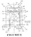
- FIG. 3shows a general diagram of an apparatus for formation of high dielectric constant metal oxide according to the present invention.
- FIG. 1 and FIGS. 2A-2Cshall be used to describe the process of forming metal oxide according to the present invention, e.g., metal oxide gate dielectric, while the apparatus for forming a metal oxide shall be described with reference to FIG. 3 .
- the various processes and the steps thereof described with reference to the figuresmay be utilized in various configurations and/or applications.
- the present inventionmay be used in the formation of gate dielectrics, dielectrics for capacitors, or for any other applications requiring a dielectric or insulating material.
- the present inventionmay be particularly beneficial in the fabrication of gate dielectrics for transistor applications in memory devices, e.g., DRAMs.
- semiconductor substraterefers to the base semiconductor layer, e.g., the lowest layer of silicon material in a wafer or a silicon layer deposited on another material such as silicon on sapphire.
- semiconductor substrate assemblyrefers to the semiconductor substrate or the semiconductor substrate having one or more layers or structures formed thereon or regions formed therein.
- high dielectric constantrefers to a dielectric constant greater than 3, and preferably greater than 10.
- the term “deposition temperature”will typically refer to the surface temperature of the substrate assembly or layer upon which a material is being deposited; the term “flow rate” as used herein in connection with gas flow rates will typically refer to the gas flow rate provided to a particular component or portion of a system according to the present invention; and the term “deposition pressure” will typically refer to the pressure within the chamber wherein the substrate assembly or layer upon which a material is being deposited is positioned.
- FIG. 1shows a structure 10 including a substrate assembly 12 upon which a metal oxide 14 is formed.
- the substrate assembly 12may be either a semiconductor substrate or a semiconductor substrate having one or more layers, structures, or regions formed thereon or therein.
- the substrate assembly 12is a silicon substrate.
- the metal oxide 14may be any high dielectric metal oxide.
- the metal oxideincludes at least one of TiO 2 , Y 2 O 3 , Al 2 O 3 , ZrO 2 , HfO 2 , Y 2 O 3 —ZrO 2 , ZrSiO 4 , LaAlO 3 , or MgAl 2 O 4 . More preferably, the metal oxide is TiO 2 .
- the present inventionmay be beneficial in forming any of the high dielectric constant materials listed above, for simplicity purposes, and preferably, the remainder of the description below is provided with respect to the formation of TiO 2 , e.g., formation of TiO 2 for a gate dielectric.
- the present inventionwill primarily be described with reference to the formation of a metal oxide for a gate dielectric as described with reference to FIGS. 2A-2C.
- the metal oxidemay be used for any other application as shown generally with reference to FIG. 1 wherein the substrate assembly 12 may be either a semiconductor substrate or, for example, a semiconductor substrate assembly including an electrode region upon which a metal oxide is formed, e.g., a capacitor application.
- FIGS. 2A-2Ca simplified flow process for forming a gate 25 (see FIG. 2C) is shown.
- a device structure 20is fabricated in accordance with conventional processing techniques prior to the formation of metal oxide 26 on the device structure 20 .
- the device structure 20includes field oxide regions 24 and active areas, i.e., those regions of a substrate 22 not covered by field oxide regions 24 .
- doped source/drain regions 32 - 33are formed as known to one skilled in the art.
- metal oxide 26is formed over the field oxide regions 24 and semiconductor substrate 22 as described further below.
- various other layers 28 - 30may be used to form a conductive gate electrode relative to the gate dielectric 26 .
- the gate dielectric and the multiple conductive layers 28 - 30are patterned resulting in gate dielectric 36 and gate electrode layers 38 - 40 to form the gate 25 .
- Various techniques for patterning the layerse.g., removing unmasked regions, are know to those skilled in the art and the present invention is not limited to any particular technique.
- Channel 23is electrically connected to source/drain 32 - 33 such that when a voltage difference exists between the source/drain, current will tend to flow through the channel 23 .
- the semiconducting characteristics of channel. 23are altered such that its resistivity may be controlled by the voltage applied to gate 25 . Thus, by changing the voltage on gate 25 , more or less current can be made to flow through channel 23 .
- the conductive gate components 38 - 40 and channel 23are separated by gate dielectric 36 .
- the metal oxide gate dielectric 36is insulative such that between the conductive gate components 38 - 40 and channel 23 little or no current flows during operation.
- the metal oxide gate dielectric 36allows the gate voltage to induce an electric field in channel 23 .
- various processing techniquessuch as, for example, metalization techniques used for providing electrical connection to the source/drain 32 , 33 and the gate 25 , are used to complete formation of, for example, the complete transistor device, interconnect levels, memory device structures including capacitive structures formed thereafter, etc.
- the present inventionis focused on the formation of the metal oxide gate dielectric 36 and the other steps utilized therewith may be those known to one skilled in the art.
- various manners of doping the source and drainmay be used, one or more layers may be used for formation of the conductive gate electrode portion of gate 25 (e.g., polycide structures, silicide layers, etc.), various silicidation processes or salicidation may be used for metalization of the various regions, etc., without limiting the process of forming the metal oxide gate electrode 36 .
- the present inventionforms TiO 2 by electron beam evaporation from a TiO 2 source, e.g., high purity TiO 2 slug, in a vacuum chamber in the presence of an ion beam.
- a TiO 2 sourcee.g., high purity TiO 2 slug
- the TiO 2is formed on a heated substrate assembly, and also in the presence of an oxygen atmosphere, e.g., O 2 or ozone.
- an oxygen atmospheree.g., O 2 or ozone.
- the metal oxide film producedprovides an adequate equivalent oxide thickness, with the metal oxide thickness of the material formed being in the range of about 50 ⁇ to about 500 ⁇ . Since tunneling currents are exponential functions of electric fields, the thicker films of TiO 2 will result in much lower electric fields and insignificant tunneling currents when compared to the use of silicon dioxide.
- TiO 2The formation of TiO 2 according to the present invention shall be further described with reference to the metal oxide evaporation system 50 shown in FIG. 3 .
- the metal oxide evaporation system 50includes a vacuum chamber 52 in which a substrate assembly, e.g., wafer 62 , is positioned and held by substrate holder 64 .
- the substrate assemblye.g., wafer 62
- the substrate assemblymay be any substrate assembly as previously described herein and it may be held in the vacuum chamber 52 by any suitable substrate holder, e.g., electrical or mechanical coupling structures.
- the metal oxide evaporation system 50further includes a heater apparatus 66 for heating the substrate assembly 62 as the metal oxide 26 is formed.
- the evaporation system 50further includes electron beam evaporation apparatus 74 in which a stream of electrons is accelerated to a high energy and directed at source material 106 to be evaporated. The electron stream melts and evaporates the material 106 for deposition of the metal oxide on surface 63 of substrate assembly 62 .
- the evaporation system 50includes ion beam apparatus 78 and ozonizer apparatus 76 .
- the ion beam apparatus 78provides for the generation of an ion beam using an inert gas to provide inert gas ions for contacting, e.g., such as for compacting, the metal oxide during formation thereof.
- the ozonizer apparatus 76compensates for the loss of oxygen in the deposited TiO 2 .
- a shutter 80e.g., a mechanical shutter, located between the substrate assembly 62 and electron beam evaporation apparatus 74 .
- a monitoring apparatus 82e.g., a quartz crystal thickness monitor, is further provided as described below.
- the heater apparatus 66may be any apparatus suitable for heating the substrate assembly 62 .
- the substrate assembly temperatureis between about 100° C. to about 150° C.
- one suitable embodiment of the heater apparatus 66includes a heating element 68 surrounded by a heat reflector 70 for reflecting heat to the substrate assembly 62 .
- the electron beam evaporation apparatus 74generally includes an electron beam gun 104 for generating an electron beam 102 directed at an evaporant source 106 to melt evaporant material thereof.
- the electron beam 102can melt and evaporate material of source 106 , provided the beam 102 can supply energy to the evaporant at an equal or greater rate than the rate at which heat is lost as the material is held at high temperature.
- Electron beam gunsare available that supply up to 10 kilowatts of highly concentrated electron beam power for evaporation applications. Very high film deposition rates can thereby be attained as a result of the high power available.
- the electron beam evaporation apparatus 74further includes a controller 108 , shown generally in FIG.
- the controller 108adjusts the electron gun power such that the gun will yield a deposition rate of about 0.1 nm/sec to 1.0 nm/sec when used in forming metal oxides according to the present invention, particularly with respect to TiO 2 .
- the beam energyis concentrated on the surface of the evaporant source 106 , and thus, a molten region can be supported by a cooled structure.
- the target material, or evaporant source itselftypically provides a solid layer that separates the molten portion of the evaporant material from a holder, e.g., a crucible, that is cooled. This eliminates the problem of reaction with or dissolution of the holder by the melt and allows highly pure films to be deposited.
- This holderis typically copper, which has a high melting temperature.
- the evaporant source 106includes high purity metal oxide.
- high purity metal oxiderefers to a metal oxide having a purity that is about 99.999% or greater.
- the evaporant source 106includes TiO 2 that is greater than about 99.999% pure.
- the electron beam gun 104is generally a self-accelerating, 270° beam gun that is generally a standard design and commonly available. In such guns, a magnetic field simultaneously bends the beam 102 to 270° and focuses the beam on the evaporant source 106 .
- the electron emission surfaceis hidden from the evaporating source 106 , and the substrates are also protected from contamination by material evaporating from the heated filament of the gun. Movement of the beam 102 , which allows the evaporant source to be scanned, may be accomplished by electromagnetic deflection. This avoids the problem of non-uniform deposition that may be caused by the formation of a cavity in the molten evaporant source if the beam 102 were stationary.
- any suitable electron beam gunmay be used according to the present invention, e.g., a Temescal electron beam gun).
- the ion beam apparatus 78which provides for bombardment of the substrate assembly surface 63 uniformly during metal oxide formation includes an ion gun 120 , an ion gas source 122 , and an ion beam controller 124 .
- the ion beam apparatus 78provides for compacting of the metal oxide formed on the surface 63 of substrate assembly 62 .
- the ion gas source 122may be any inert gas.
- inertmeans any gas that is nonreactive with the materials being deposited.
- the ion gas sourceincludes at least one of argon, xenon, and krypton. More preferably, the ion gas source is argon.
- the ion gun 120may be any suitable type of ion gun that provides for compaction of the metal oxide being formed, such as a Kaufman-type ion gun. Ion guns are commonly available, such as those available from Applied Materials, Inc. Preferably, the ion beam incident angle ( ⁇ ) is within the range of +40 degrees to about ⁇ 40 degrees relative to the surface 63 as shown in FIG. 3 . Further preferably, the ion beam gun 120 is an ion gun with a fairly large diameter. Preferably, the diameter is in the range of 7.6 cm to 10 cm. Yet further, the ion gun is preferably a filament-type gun which uses a hot filament to ionize the gas from gas source 122 . A filament-type ion gun is preferred over a cold catheter discharge ion gun.
- the ion beam gun 120is controlled by controller 124 to produce an ion beam density for bombardment of the material being formed on surface 63 .
- the ion beam densityis in the range of about 0.5 ma/cm 2 to about 1.0 ma/cm 2 .
- An ion beam density in this rangeis generally required to obtain a suitable degree of compaction by the bombardment of ions on substrate assembly surface 63 as the metal oxide is being formed.
- the ozonizer apparatus 76provides the necessary oxygen to compensate for any loss of oxygen in the evaporated metal oxide.
- the ozonizer apparatus 76includes the ozonizer structure 132 for providing ozone into the vacuum chamber 52 from the ozone source 130 under the control of controller 136 .
- the vacuum chamber 52may be flooded with oxygen, e.g., O 2 or O 3
- the ozonizer structure 132is preferably adapted to direct ozone towards the surface 63 of the substrate assembly 62 upon which the metal oxide is deposited. This maintains the ozone in the region of formation of the metal oxide on the surface 63 and provides for uniform distribution of ozone in this region.
- the ozonizer structure 132includes a ring 133 with center axis 81 therethrough.
- the ring 133has a plurality of openings 135 adapted to direct ozone towards the surface 63 of the substrate assembly 62 .
- the ring 133 having the openings 135enhance the uniform distribution of ozone in the region of the surface 63 .
- the ozonizer ring 133is positioned generally parallel with the substrate assembly 62 , e.g., semiconductor wafer, with the openings 135 adapted for directing ozone towards the surface 63 .
- the ozonizer ring 133is generally of a size that does not inhibit the ion beam generated by the ion beam gun 120 from bombardment of the surface 63 as the metal oxide is formed.
- the metal oxide evaporation system 50further includes a shutter 80 , e.g., a mechanical shutter, located between the substrate assembly 62 and the electron beam gun 104 in the vacuum chamber 52 .
- the shutter 80is employed to prevent contaminants absorbed on the evaporant source surface from being incorporated into deposited metal oxide. In other words, if the vacuum chamber and the evaporant source are exposed to ambient conditions in the loading and unloading of substrate assemblies, e.g.,wafers, some contamination may occur on the evaporant source. Therefore, when the source is initially heated, such surface contaminants may vaporize together with source material and, as such, contaminate the metal oxide formed on surface 63 . By interposing the shutter between the evaporant source 106 and the surface 63 and postponing formation of the metal oxide until the evaporant source 106 is sufficiently clean, the purity of the formed metal oxide can be enhanced.
- monitoring apparatus 82which monitors the metal oxide thickness being formed on substrate surface 63 . Further, incorporation of oxygen in the film may also be monitored. Various types of monitoring apparatus 82 may be used, such as a quartz crystal thickness monitor or an oxygen pressure monitor for monitoring oxygen incorporation. Such monitoring may provide information to one or more of the controllers of the system 50 . For example, the concentration of ozone in the vacuum chamber 52 may be controlled by monitoring the oxygen content in the film using monitoring apparatus 82 and adjusting, via controller 136 , the ozone in the region proximate the surface 63 of substrate assembly 62 . Likewise, the deposition rate may be adjusted under control of controller 108 as a result of information available from monitoring apparatus 82 , concerning the thickness of the metal oxide being formed on surface 63 . Although several monitoring devices are described above, the present invention is not limited to those listed.
- the vacuum chamber 52includes an elongated chamber space extending between a first end 160 and a second end 161 along axis 81 .
- the electron beam gun 104is centrally located toward the bottom or second end 161 of the vacuum chamber 52 .
- the substrate assembly holder 64which holds the substrate assembly 62 is surrounded by the heater apparatus 66 at the first end 160 of the vacuum chamber 52 .
- Proximate the substrate assembly 62is the ozonizer ring 133 with the small openings 135 directed to the substrate assembly 62 for uniform distribution of ozone, particularly to compensate for loss of oxygen in an evaporated TiO 2 film.
- the shutter 80is located between the substrate assembly 62 and the ozonizer ring 133 .
- the ion beam gun 120is located generally towards the substrate assembly 62 relative to the ion electron beam gun 104 and slightly off axis from the center location of the electron beam gun 104 .
- the method of forming metal oxide using, for example, the evaporation system 50 described with reference to FIG. 3shall be described below.
- the description of the formation method belowis provided with respect to TiO 2 formation, however, the general concepts employed in the formation method are applicable to the other high dielectric constant materials as listed previously herein.
- the vacuum chamber 52is pumped down to a pressure in the range of about 2 ⁇ 10 ⁇ 6 torr to about 8 ⁇ 10 ⁇ 6 torr as generally represented by arrow 54 .
- the heater apparatus 66is controlled to provide a deposition temperature of about 100° C. to about 150° C.
- the evaporant source 106is a high purity TiO 2 slug.
- the controller 108initializes the evaporation process.
- the ion beam gun 120may be initiated by controller 124 simultaneously with the electron beam evaporation apparatus 74 , preferably, the introduction of the ion beam used to bombard the substrate assembly surface 63 during the metal oxide formation from the evaporation of the evaporant source 106 is delayed for a predetermined period of time to allow deposition of at least one monolayer of the metal oxide, e.g., TiO 2 .
- the electron beam gun poweris adjusted such that the gun will yield a deposition rate of about 0.1 nm/sec to 1.0 nm/sec.
- the ion beam apparatus 78provides an argon ion beam density in the range of about 0.5 ma/cm 2 to 1 ma/cm 2 .
- the ion beamis delayed following initialization of the evaporation apparatus for a period of time, e.g., approximately 1-2 seconds, to allow deposition of at least one monolayer of TiO 2 .
- a pre-evaporation phaseis completed during which shutter 80 is closed, preventing formation of metal oxide on surface 63 .
- outgasses resulting from evaporation during the pre-evaporation phaseare exhausted, as is generally represented by arrow 55 . As such, contaminants which potentially may contaminate the metal oxide film being formed are removed during the pre-evaporation phase.
- the shutter 80is opened to allow formation of the metal oxide on surface 63 .
- the argon beaminitiated to provide for compaction during the remaining formation of the TiO 2 .
- the partial pressure of ozone provided by the ozonizer apparatus 76 in the vacuum chamber 52is in the range of about 2 ⁇ 10 ⁇ 5 torr about 8 ⁇ 10 ⁇ 5 torr.
- the optimum parameters for the ozone in the region proximate the substrate assembly 62is or may be determined by monitoring the oxygen content in the metal oxide being formed as represented generally by the monitoring apparatus 82 .
- the TiO 2 thicknessis in the range as described previously herein with reference to FIGS. 2A-2C.
- Typical packing densities for the metal oxideare preferably in the range of about 0.9 to about 1.0.
- the ratio of a metal oxide film deposited without the use of ion bombardment versus a metal oxide film deposited using ion bombardmentis in the range of about 0.9 to about 1.0.
Landscapes
- Chemical & Material Sciences (AREA)
- Engineering & Computer Science (AREA)
- Chemical Kinetics & Catalysis (AREA)
- Metallurgy (AREA)
- Organic Chemistry (AREA)
- Mechanical Engineering (AREA)
- Materials Engineering (AREA)
- Power Engineering (AREA)
- General Physics & Mathematics (AREA)
- Condensed Matter Physics & Semiconductors (AREA)
- Microelectronics & Electronic Packaging (AREA)
- Computer Hardware Design (AREA)
- Physics & Mathematics (AREA)
- Manufacturing & Machinery (AREA)
- Crystallography & Structural Chemistry (AREA)
- General Chemical & Material Sciences (AREA)
- Formation Of Insulating Films (AREA)
- Physical Vapour Deposition (AREA)
Abstract
Description
Claims (10)
Priority Applications (1)
| Application Number | Priority Date | Filing Date | Title |
|---|---|---|---|
| US10/227,699US6608378B2 (en) | 2001-02-09 | 2002-08-26 | Formation of metal oxide gate dielectric |
Applications Claiming Priority (2)
| Application Number | Priority Date | Filing Date | Title |
|---|---|---|---|
| US09/779,959US6495436B2 (en) | 2001-02-09 | 2001-02-09 | Formation of metal oxide gate dielectric |
| US10/227,699US6608378B2 (en) | 2001-02-09 | 2002-08-26 | Formation of metal oxide gate dielectric |
Related Parent Applications (1)
| Application Number | Title | Priority Date | Filing Date |
|---|---|---|---|
| US09/779,959DivisionUS6495436B2 (en) | 2001-02-09 | 2001-02-09 | Formation of metal oxide gate dielectric |
Publications (2)
| Publication Number | Publication Date |
|---|---|
| US20030003702A1 US20030003702A1 (en) | 2003-01-02 |
| US6608378B2true US6608378B2 (en) | 2003-08-19 |
Family
ID=25118118
Family Applications (2)
| Application Number | Title | Priority Date | Filing Date |
|---|---|---|---|
| US09/779,959Expired - Fee RelatedUS6495436B2 (en) | 2001-02-09 | 2001-02-09 | Formation of metal oxide gate dielectric |
| US10/227,699Expired - LifetimeUS6608378B2 (en) | 2001-02-09 | 2002-08-26 | Formation of metal oxide gate dielectric |
Family Applications Before (1)
| Application Number | Title | Priority Date | Filing Date |
|---|---|---|---|
| US09/779,959Expired - Fee RelatedUS6495436B2 (en) | 2001-02-09 | 2001-02-09 | Formation of metal oxide gate dielectric |
Country Status (2)
| Country | Link |
|---|---|
| US (2) | US6495436B2 (en) |
| WO (1) | WO2002065537A2 (en) |
Cited By (50)
| Publication number | Priority date | Publication date | Assignee | Title |
|---|---|---|---|---|
| US20030045060A1 (en)* | 2001-08-30 | 2003-03-06 | Micron Technology, Inc. | Crystalline or amorphous medium-k gate oxides, Y2O3 and Gd2O3 |
| US6790791B2 (en) | 2002-08-15 | 2004-09-14 | Micron Technology, Inc. | Lanthanide doped TiOx dielectric films |
| US20040183108A1 (en)* | 2001-12-20 | 2004-09-23 | Micron Technology, Inc. | Low-temperature grown high-quality ultra-thin praseodymium gate dielectrics |
| US20040262700A1 (en)* | 2003-06-24 | 2004-12-30 | Micron Technology, Inc. | Lanthanide oxide / hafnium oxide dielectrics |
| US6852167B2 (en) | 2001-03-01 | 2005-02-08 | Micron Technology, Inc. | Methods, systems, and apparatus for uniform chemical-vapor depositions |
| US20050032317A1 (en)* | 2003-08-06 | 2005-02-10 | Sandhu Gurtej S. | Methods of forming material on a substrate, and a method of forming a field effect transistor gate oxide on a substrate |
| US6953730B2 (en) | 2001-12-20 | 2005-10-11 | Micron Technology, Inc. | Low-temperature grown high quality ultra-thin CoTiO3 gate dielectrics |
| US7081421B2 (en) | 2004-08-26 | 2006-07-25 | Micron Technology, Inc. | Lanthanide oxide dielectric layer |
| US7084078B2 (en) | 2002-08-29 | 2006-08-01 | Micron Technology, Inc. | Atomic layer deposited lanthanide doped TiOx dielectric films |
| US20060176645A1 (en)* | 2005-02-08 | 2006-08-10 | Micron Technology, Inc. | Atomic layer deposition of Dy doped HfO2 films as gate dielectrics |
| US20060183272A1 (en)* | 2005-02-15 | 2006-08-17 | Micron Technology, Inc. | Atomic layer deposition of Zr3N4/ZrO2 films as gate dielectrics |
| US20060189154A1 (en)* | 2005-02-23 | 2006-08-24 | Micron Technology, Inc. | Atomic layer deposition of Hf3N4/HfO2 films as gate dielectrics |
| US20060244100A1 (en)* | 2005-04-28 | 2006-11-02 | Micron Technology, Inc. | Atomic layer deposited zirconium silicon oxide films |
| US7135369B2 (en) | 2003-03-31 | 2006-11-14 | Micron Technology, Inc. | Atomic layer deposited ZrAlxOy dielectric layers including Zr4AlO9 |
| US20070037415A1 (en)* | 2004-12-13 | 2007-02-15 | Micron Technology, Inc. | Lanthanum hafnium oxide dielectrics |
| US7183186B2 (en) | 2003-04-22 | 2007-02-27 | Micro Technology, Inc. | Atomic layer deposited ZrTiO4 films |
| US7192824B2 (en) | 2003-06-24 | 2007-03-20 | Micron Technology, Inc. | Lanthanide oxide / hafnium oxide dielectric layers |
| US7192892B2 (en) | 2003-03-04 | 2007-03-20 | Micron Technology, Inc. | Atomic layer deposited dielectric layers |
| US7205218B2 (en) | 2002-06-05 | 2007-04-17 | Micron Technology, Inc. | Method including forming gate dielectrics having multiple lanthanide oxide layers |
| US7205620B2 (en) | 2002-01-17 | 2007-04-17 | Micron Technology, Inc. | Highly reliable amorphous high-k gate dielectric ZrOxNy |
| US7259434B2 (en) | 2001-08-30 | 2007-08-21 | Micron Technology, Inc. | Highly reliable amorphous high-k gate oxide ZrO2 |
| US20070234949A1 (en)* | 2006-04-07 | 2007-10-11 | Micron Technology, Inc. | Atomic layer deposited titanium-doped indium oxide films |
| US7374964B2 (en) | 2005-02-10 | 2008-05-20 | Micron Technology, Inc. | Atomic layer deposition of CeO2/Al2O3 films as gate dielectrics |
| US7393736B2 (en) | 2005-08-29 | 2008-07-01 | Micron Technology, Inc. | Atomic layer deposition of Zrx Hfy Sn1-x-y O2 films as high k gate dielectrics |
| US7402876B2 (en) | 2002-12-04 | 2008-07-22 | Micron Technology, Inc. | Zr— Sn—Ti—O films |
| US7410910B2 (en) | 2005-08-31 | 2008-08-12 | Micron Technology, Inc. | Lanthanum aluminum oxynitride dielectric films |
| US7446368B2 (en) | 2001-08-30 | 2008-11-04 | Micron Technology, Inc. | Deposition of metal oxide and/or low asymmetrical tunnel barrier interpoly insulators |
| US7494939B2 (en) | 2004-08-31 | 2009-02-24 | Micron Technology, Inc. | Methods for forming a lanthanum-metal oxide dielectric layer |
| US7544596B2 (en) | 2005-08-30 | 2009-06-09 | Micron Technology, Inc. | Atomic layer deposition of GdScO3 films as gate dielectrics |
| US7554161B2 (en) | 2002-06-05 | 2009-06-30 | Micron Technology, Inc. | HfAlO3 films for gate dielectrics |
| US20090166185A1 (en)* | 2007-12-27 | 2009-07-02 | Hon Hai Precision Industry Co., Ltd. | Ion assisted deposition method for forming multilayer film |
| US7560395B2 (en) | 2005-01-05 | 2009-07-14 | Micron Technology, Inc. | Atomic layer deposited hafnium tantalum oxide dielectrics |
| US7560793B2 (en) | 2002-05-02 | 2009-07-14 | Micron Technology, Inc. | Atomic layer deposition and conversion |
| US7572695B2 (en) | 2005-05-27 | 2009-08-11 | Micron Technology, Inc. | Hafnium titanium oxide films |
| US7582549B2 (en) | 2006-08-25 | 2009-09-01 | Micron Technology, Inc. | Atomic layer deposited barium strontium titanium oxide films |
| US7588988B2 (en) | 2004-08-31 | 2009-09-15 | Micron Technology, Inc. | Method of forming apparatus having oxide films formed using atomic layer deposition |
| US7601649B2 (en) | 2004-08-02 | 2009-10-13 | Micron Technology, Inc. | Zirconium-doped tantalum oxide films |
| US7611959B2 (en) | 2002-12-04 | 2009-11-03 | Micron Technology, Inc. | Zr-Sn-Ti-O films |
| US7662729B2 (en) | 2005-04-28 | 2010-02-16 | Micron Technology, Inc. | Atomic layer deposition of a ruthenium layer to a lanthanide oxide dielectric layer |
| US7670646B2 (en) | 2002-05-02 | 2010-03-02 | Micron Technology, Inc. | Methods for atomic-layer deposition |
| US7687409B2 (en) | 2005-03-29 | 2010-03-30 | Micron Technology, Inc. | Atomic layer deposited titanium silicon oxide films |
| US7709402B2 (en) | 2006-02-16 | 2010-05-04 | Micron Technology, Inc. | Conductive layers for hafnium silicon oxynitride films |
| US7728626B2 (en) | 2002-07-08 | 2010-06-01 | Micron Technology, Inc. | Memory utilizing oxide nanolaminates |
| US7869242B2 (en) | 1999-07-30 | 2011-01-11 | Micron Technology, Inc. | Transmission lines for CMOS integrated circuits |
| US7972974B2 (en) | 2006-01-10 | 2011-07-05 | Micron Technology, Inc. | Gallium lanthanide oxide films |
| US8071476B2 (en) | 2005-08-31 | 2011-12-06 | Micron Technology, Inc. | Cobalt titanium oxide dielectric films |
| US8125038B2 (en) | 2002-07-30 | 2012-02-28 | Micron Technology, Inc. | Nanolaminates of hafnium oxide and zirconium oxide |
| US8501563B2 (en) | 2005-07-20 | 2013-08-06 | Micron Technology, Inc. | Devices with nanocrystals and methods of formation |
| US8962078B2 (en) | 2012-06-22 | 2015-02-24 | Tokyo Electron Limited | Method for depositing dielectric films |
| RU172351U1 (en)* | 2017-04-17 | 2017-07-05 | Федеральное государственное бюджетное образовательное учреждение высшего образования "Томский государственный университет систем управления и радиоэлектроники" | Device for electron beam deposition of oxide coatings |
Families Citing this family (44)
| Publication number | Priority date | Publication date | Assignee | Title |
|---|---|---|---|---|
| US6495436B2 (en) | 2001-02-09 | 2002-12-17 | Micron Technology, Inc. | Formation of metal oxide gate dielectric |
| US6818493B2 (en)* | 2001-07-26 | 2004-11-16 | Motorola, Inc. | Selective metal oxide removal performed in a reaction chamber in the absence of RF activation |
| US7068544B2 (en)* | 2001-08-30 | 2006-06-27 | Micron Technology, Inc. | Flash memory with low tunnel barrier interpoly insulators |
| US6893984B2 (en)* | 2002-02-20 | 2005-05-17 | Micron Technology Inc. | Evaporated LaA1O3 films for gate dielectrics |
| US6812100B2 (en) | 2002-03-13 | 2004-11-02 | Micron Technology, Inc. | Evaporation of Y-Si-O films for medium-k dielectrics |
| US7045430B2 (en)* | 2002-05-02 | 2006-05-16 | Micron Technology Inc. | Atomic layer-deposited LaAlO3 films for gate dielectrics |
| US7193893B2 (en) | 2002-06-21 | 2007-03-20 | Micron Technology, Inc. | Write once read only memory employing floating gates |
| US6970370B2 (en) | 2002-06-21 | 2005-11-29 | Micron Technology, Inc. | Ferroelectric write once read only memory for archival storage |
| US7154140B2 (en) | 2002-06-21 | 2006-12-26 | Micron Technology, Inc. | Write once read only memory with large work function floating gates |
| US6804136B2 (en) | 2002-06-21 | 2004-10-12 | Micron Technology, Inc. | Write once read only memory employing charge trapping in insulators |
| US7221017B2 (en) | 2002-07-08 | 2007-05-22 | Micron Technology, Inc. | Memory utilizing oxide-conductor nanolaminates |
| US6884739B2 (en) | 2002-08-15 | 2005-04-26 | Micron Technology Inc. | Lanthanide doped TiOx dielectric films by plasma oxidation |
| US20040036129A1 (en) | 2002-08-22 | 2004-02-26 | Micron Technology, Inc. | Atomic layer deposition of CMOS gates with variable work functions |
| US6967154B2 (en) | 2002-08-26 | 2005-11-22 | Micron Technology, Inc. | Enhanced atomic layer deposition |
| US7199023B2 (en)* | 2002-08-28 | 2007-04-03 | Micron Technology, Inc. | Atomic layer deposited HfSiON dielectric films wherein each precursor is independendently pulsed |
| JP4933256B2 (en)* | 2003-07-31 | 2012-05-16 | 東京エレクトロン株式会社 | Method for forming a semiconductor microstructure |
| US7202186B2 (en) | 2003-07-31 | 2007-04-10 | Tokyo Electron Limited | Method of forming uniform ultra-thin oxynitride layers |
| US7235440B2 (en) | 2003-07-31 | 2007-06-26 | Tokyo Electron Limited | Formation of ultra-thin oxide layers by self-limiting interfacial oxidation |
| FR2859487B1 (en)* | 2003-09-04 | 2006-12-15 | Essilor Int | METHOD FOR DEPOSITING AN AMORPHOUS LAYER CONTAINING MAJORITARILY FLUORINE AND CARBON AND DEVICE SUITABLE FOR ITS IMPLEMENTATION |
| US7157769B2 (en)* | 2003-12-18 | 2007-01-02 | Micron Technology, Inc. | Flash memory having a high-permittivity tunnel dielectric |
| US20050233477A1 (en)* | 2004-03-05 | 2005-10-20 | Tokyo Electron Limited | Substrate processing apparatus, substrate processing method, and program for implementing the method |
| US20060125030A1 (en)* | 2004-12-13 | 2006-06-15 | Micron Technology, Inc. | Hybrid ALD-CVD of PrxOy/ZrO2 films as gate dielectrics |
| US7510983B2 (en) | 2005-06-14 | 2009-03-31 | Micron Technology, Inc. | Iridium/zirconium oxide structure |
| US7195999B2 (en)* | 2005-07-07 | 2007-03-27 | Micron Technology, Inc. | Metal-substituted transistor gates |
| US7473637B2 (en) | 2005-07-20 | 2009-01-06 | Micron Technology, Inc. | ALD formed titanium nitride films |
| US20070049023A1 (en)* | 2005-08-29 | 2007-03-01 | Micron Technology, Inc. | Zirconium-doped gadolinium oxide films |
| US7214994B2 (en) | 2005-08-31 | 2007-05-08 | Micron Technology, Inc. | Self aligned metal gates on high-k dielectrics |
| US7985995B2 (en) | 2006-08-03 | 2011-07-26 | Micron Technology, Inc. | Zr-substituted BaTiO3 films |
| US7727908B2 (en) | 2006-08-03 | 2010-06-01 | Micron Technology, Inc. | Deposition of ZrA1ON films |
| US7749879B2 (en)* | 2006-08-03 | 2010-07-06 | Micron Technology, Inc. | ALD of silicon films on germanium |
| US7563730B2 (en) | 2006-08-31 | 2009-07-21 | Micron Technology, Inc. | Hafnium lanthanide oxynitride films |
| US7776765B2 (en) | 2006-08-31 | 2010-08-17 | Micron Technology, Inc. | Tantalum silicon oxynitride high-k dielectrics and metal gates |
| US7544604B2 (en) | 2006-08-31 | 2009-06-09 | Micron Technology, Inc. | Tantalum lanthanide oxynitride films |
| US7759747B2 (en) | 2006-08-31 | 2010-07-20 | Micron Technology, Inc. | Tantalum aluminum oxynitride high-κ dielectric |
| US7432548B2 (en) | 2006-08-31 | 2008-10-07 | Micron Technology, Inc. | Silicon lanthanide oxynitride films |
| US7605030B2 (en) | 2006-08-31 | 2009-10-20 | Micron Technology, Inc. | Hafnium tantalum oxynitride high-k dielectric and metal gates |
| US20080087890A1 (en)* | 2006-10-16 | 2008-04-17 | Micron Technology, Inc. | Methods to form dielectric structures in semiconductor devices and resulting devices |
| US7498230B2 (en)* | 2007-02-13 | 2009-03-03 | Micron Technology, Inc. | Magnesium-doped zinc oxide structures and methods |
| US8367506B2 (en) | 2007-06-04 | 2013-02-05 | Micron Technology, Inc. | High-k dielectrics with gold nano-particles |
| US7759237B2 (en)* | 2007-06-28 | 2010-07-20 | Micron Technology, Inc. | Method of forming lutetium and lanthanum dielectric structures |
| DE102008050074A1 (en)* | 2008-04-30 | 2009-11-12 | Von Ardenne Anlagentechnik Gmbh | Method and arrangement for generating contacts on carrier substrate-free photovoltaic elements |
| JP2013185158A (en)* | 2012-03-05 | 2013-09-19 | Optorun Co Ltd | Film deposition method |
| US9773889B2 (en)* | 2014-07-18 | 2017-09-26 | Taiwan Semiconductor Manufacturing Company Limited | Method of semiconductor arrangement formation |
| CN111809154B (en)* | 2020-06-23 | 2021-07-23 | 奥趋光电技术(杭州)有限公司 | Method for preparing high-quality silicon-based aluminum nitride template |
Citations (20)
| Publication number | Priority date | Publication date | Assignee | Title |
|---|---|---|---|---|
| EP0269112A2 (en) | 1986-11-27 | 1988-06-01 | Nissin Electric Company, Limited | Method of forming a thin crystalline metal film |
| JPS63170244A (en) | 1987-01-08 | 1988-07-14 | Matsushita Electric Ind Co Ltd | Method of forming anti-reflection film |
| US4759948A (en) | 1986-01-29 | 1988-07-26 | Hitachi, Ltd. | Film formation through co-deposition with high and low energy beams |
| US4793908A (en)* | 1986-12-29 | 1988-12-27 | Rockwell International Corporation | Multiple ion source method and apparatus for fabricating multilayer optical films |
| US4933058A (en) | 1986-01-23 | 1990-06-12 | The Gillette Company | Formation of hard coatings on cutting edges |
| US4987102A (en) | 1989-12-04 | 1991-01-22 | Motorola, Inc. | Process for forming high purity thin films |
| JPH03202468A (en) | 1989-12-29 | 1991-09-04 | Nissin Electric Co Ltd | Film formation |
| US5055319A (en) | 1990-04-02 | 1991-10-08 | The Regents Of The University Of California | Controlled high rate deposition of metal oxide films |
| US5055169A (en)* | 1989-03-17 | 1991-10-08 | The United States Of America As Represented By The Secretary Of The Army | Method of making mixed metal oxide coated substrates |
| EP0468758A1 (en) | 1990-07-24 | 1992-01-29 | Semiconductor Energy Laboratory Co., Ltd. | Method of forming insulating films, capacitances, and semiconductor devices |
| US5122483A (en) | 1989-12-29 | 1992-06-16 | Nissin Electric Company, Limited | Method of forming a highly insulative thin films |
| US5250327A (en)* | 1986-04-28 | 1993-10-05 | Nissin Electric Co. Ltd. | Composite substrate and process for producing the same |
| EP0565766A2 (en) | 1992-02-20 | 1993-10-20 | Nissin Electric Company, Limited | Copper film coated substrate and method of forming copper film on substrate |
| EP0570618A1 (en) | 1992-05-21 | 1993-11-24 | Nissin Electric Company, Limited | Film forming method and apparatus |
| WO1998055293A1 (en) | 1997-06-06 | 1998-12-10 | Corning Incorporated | Method of forming a silicon layer on a surface |
| US5849370A (en) | 1995-04-14 | 1998-12-15 | Spectra-Physics Lasers, Inc. | Method for producing low scatter, low loss, environmentally stable dielectric coatings |
| US6020243A (en) | 1997-07-24 | 2000-02-01 | Texas Instruments Incorporated | Zirconium and/or hafnium silicon-oxynitride gate dielectric |
| US6251230B1 (en)* | 1994-08-18 | 2001-06-26 | Matsushita Electric Industrial Co., Ltd. | Method and device for manufacturing a thin film and magnestic recording medium |
| US6294479B1 (en)* | 1992-05-21 | 2001-09-25 | Nissin Electric Co., Ltd | Film forming method and apparatus |
| US20020111001A1 (en) | 2001-02-09 | 2002-08-15 | Micron Technology, Inc. | Formation of metal oxide gate dielectric |
- 2001
- 2001-02-09USUS09/779,959patent/US6495436B2/ennot_activeExpired - Fee Related
- 2002
- 2002-01-31WOPCT/US2002/003115patent/WO2002065537A2/ennot_activeApplication Discontinuation
- 2002-08-26USUS10/227,699patent/US6608378B2/ennot_activeExpired - Lifetime
Patent Citations (21)
| Publication number | Priority date | Publication date | Assignee | Title |
|---|---|---|---|---|
| US4933058A (en) | 1986-01-23 | 1990-06-12 | The Gillette Company | Formation of hard coatings on cutting edges |
| US4759948A (en) | 1986-01-29 | 1988-07-26 | Hitachi, Ltd. | Film formation through co-deposition with high and low energy beams |
| US5250327A (en)* | 1986-04-28 | 1993-10-05 | Nissin Electric Co. Ltd. | Composite substrate and process for producing the same |
| EP0269112A2 (en) | 1986-11-27 | 1988-06-01 | Nissin Electric Company, Limited | Method of forming a thin crystalline metal film |
| US4793908A (en)* | 1986-12-29 | 1988-12-27 | Rockwell International Corporation | Multiple ion source method and apparatus for fabricating multilayer optical films |
| JPS63170244A (en) | 1987-01-08 | 1988-07-14 | Matsushita Electric Ind Co Ltd | Method of forming anti-reflection film |
| US5055169A (en)* | 1989-03-17 | 1991-10-08 | The United States Of America As Represented By The Secretary Of The Army | Method of making mixed metal oxide coated substrates |
| US4987102A (en) | 1989-12-04 | 1991-01-22 | Motorola, Inc. | Process for forming high purity thin films |
| US5122483A (en) | 1989-12-29 | 1992-06-16 | Nissin Electric Company, Limited | Method of forming a highly insulative thin films |
| JPH03202468A (en) | 1989-12-29 | 1991-09-04 | Nissin Electric Co Ltd | Film formation |
| US5055319A (en) | 1990-04-02 | 1991-10-08 | The Regents Of The University Of California | Controlled high rate deposition of metal oxide films |
| EP0468758A1 (en) | 1990-07-24 | 1992-01-29 | Semiconductor Energy Laboratory Co., Ltd. | Method of forming insulating films, capacitances, and semiconductor devices |
| US6144057A (en) | 1990-07-24 | 2000-11-07 | Semiconductor Energy Laboratory Co., Ltd. | Semiconductor memory device including a field effect transistor |
| EP0565766A2 (en) | 1992-02-20 | 1993-10-20 | Nissin Electric Company, Limited | Copper film coated substrate and method of forming copper film on substrate |
| EP0570618A1 (en) | 1992-05-21 | 1993-11-24 | Nissin Electric Company, Limited | Film forming method and apparatus |
| US6294479B1 (en)* | 1992-05-21 | 2001-09-25 | Nissin Electric Co., Ltd | Film forming method and apparatus |
| US6251230B1 (en)* | 1994-08-18 | 2001-06-26 | Matsushita Electric Industrial Co., Ltd. | Method and device for manufacturing a thin film and magnestic recording medium |
| US5849370A (en) | 1995-04-14 | 1998-12-15 | Spectra-Physics Lasers, Inc. | Method for producing low scatter, low loss, environmentally stable dielectric coatings |
| WO1998055293A1 (en) | 1997-06-06 | 1998-12-10 | Corning Incorporated | Method of forming a silicon layer on a surface |
| US6020243A (en) | 1997-07-24 | 2000-02-01 | Texas Instruments Incorporated | Zirconium and/or hafnium silicon-oxynitride gate dielectric |
| US20020111001A1 (en) | 2001-02-09 | 2002-08-15 | Micron Technology, Inc. | Formation of metal oxide gate dielectric |
Non-Patent Citations (7)
| Title |
|---|
| Guo et al., "High Quality Ultra-thin (1.5nm) TiO2/Si3N4 Gate Dielectric for Deep Sub-micron CMOS Technology," IEEE Technical Digest of International Electron Devices Meeting; 1999: 137-140. |
| Haraguchi et al., "A TiO2 Gate Insulator of A 1-nm Equivalent Oxide Thickness Deposited by Electron-Beam Evaporation," Extended Abstracts of 1999 International Conference on Solid State Devices and Materials, Tokyo, Japan; Sep. 21-24, 1999: 376-377. |
| Lee et al., "Ion-assisted deposition of silver thin films," Thin Solid Films; 2000; 359(1): 95-97. |
| Lee et al., "Ultrathin Hafnium Oxide with Low Leakage and Excellent Reliability for Alternative Gate Dielectric Application," IEEE Technical Digest of International Electron Devices Meeting; 1999:133-136. |
| Luan et al., "High Quality Ta2O5 Gate Dielectrics and Tox,eq<10 Å," IEEE Technical Digest of International Electron Devices Meeting; 1999: 141-142. |
| Martin et al., "Ion-beam-assisted deposition of thin films," Applied Optics; 1983; 22(1): 178-184. |
| Souche et al., "Visible and infrared ellipsometry study of ion assisted SiO2 films," Thin Solid Films; 1998; 313-314: 676-681. |
Cited By (131)
| Publication number | Priority date | Publication date | Assignee | Title |
|---|---|---|---|---|
| US7869242B2 (en) | 1999-07-30 | 2011-01-11 | Micron Technology, Inc. | Transmission lines for CMOS integrated circuits |
| US6852167B2 (en) | 2001-03-01 | 2005-02-08 | Micron Technology, Inc. | Methods, systems, and apparatus for uniform chemical-vapor depositions |
| US7410668B2 (en) | 2001-03-01 | 2008-08-12 | Micron Technology, Inc. | Methods, systems, and apparatus for uniform chemical-vapor depositions |
| US20030045060A1 (en)* | 2001-08-30 | 2003-03-06 | Micron Technology, Inc. | Crystalline or amorphous medium-k gate oxides, Y2O3 and Gd2O3 |
| US7259434B2 (en) | 2001-08-30 | 2007-08-21 | Micron Technology, Inc. | Highly reliable amorphous high-k gate oxide ZrO2 |
| US7446368B2 (en) | 2001-08-30 | 2008-11-04 | Micron Technology, Inc. | Deposition of metal oxide and/or low asymmetrical tunnel barrier interpoly insulators |
| US8652957B2 (en) | 2001-08-30 | 2014-02-18 | Micron Technology, Inc. | High-K gate dielectric oxide |
| US7476925B2 (en) | 2001-08-30 | 2009-01-13 | Micron Technology, Inc. | Atomic layer deposition of metal oxide and/or low asymmetrical tunnel barrier interploy insulators |
| US7208804B2 (en) | 2001-08-30 | 2007-04-24 | Micron Technology, Inc. | Crystalline or amorphous medium-K gate oxides, Y203 and Gd203 |
| US8026161B2 (en) | 2001-08-30 | 2011-09-27 | Micron Technology, Inc. | Highly reliable amorphous high-K gate oxide ZrO2 |
| US6844203B2 (en) | 2001-08-30 | 2005-01-18 | Micron Technology, Inc. | Gate oxides, and methods of forming |
| US7064058B2 (en) | 2001-12-20 | 2006-06-20 | Micron Technology, Inc. | Low-temperature growth high-quality ultra-thin praseodymium gate dieletrics |
| US8178413B2 (en) | 2001-12-20 | 2012-05-15 | Micron Technology, Inc. | Low-temperature grown high quality ultra-thin CoTiO3 gate dielectrics |
| US20040183108A1 (en)* | 2001-12-20 | 2004-09-23 | Micron Technology, Inc. | Low-temperature grown high-quality ultra-thin praseodymium gate dielectrics |
| US6979855B2 (en) | 2001-12-20 | 2005-12-27 | Micron Technology, Inc. | High-quality praseodymium gate dielectrics |
| US7429515B2 (en) | 2001-12-20 | 2008-09-30 | Micron Technology, Inc. | Low-temperature grown high quality ultra-thin CoTiO3 gate dielectrics |
| US6953730B2 (en) | 2001-12-20 | 2005-10-11 | Micron Technology, Inc. | Low-temperature grown high quality ultra-thin CoTiO3 gate dielectrics |
| US7804144B2 (en) | 2001-12-20 | 2010-09-28 | Micron Technology, Inc. | Low-temperature grown high quality ultra-thin CoTiO3 gate dielectrics |
| US7205620B2 (en) | 2002-01-17 | 2007-04-17 | Micron Technology, Inc. | Highly reliable amorphous high-k gate dielectric ZrOxNy |
| US7589029B2 (en) | 2002-05-02 | 2009-09-15 | Micron Technology, Inc. | Atomic layer deposition and conversion |
| US7560793B2 (en) | 2002-05-02 | 2009-07-14 | Micron Technology, Inc. | Atomic layer deposition and conversion |
| US7670646B2 (en) | 2002-05-02 | 2010-03-02 | Micron Technology, Inc. | Methods for atomic-layer deposition |
| US8093638B2 (en) | 2002-06-05 | 2012-01-10 | Micron Technology, Inc. | Systems with a gate dielectric having multiple lanthanide oxide layers |
| US7205218B2 (en) | 2002-06-05 | 2007-04-17 | Micron Technology, Inc. | Method including forming gate dielectrics having multiple lanthanide oxide layers |
| US7554161B2 (en) | 2002-06-05 | 2009-06-30 | Micron Technology, Inc. | HfAlO3 films for gate dielectrics |
| US7728626B2 (en) | 2002-07-08 | 2010-06-01 | Micron Technology, Inc. | Memory utilizing oxide nanolaminates |
| US8228725B2 (en) | 2002-07-08 | 2012-07-24 | Micron Technology, Inc. | Memory utilizing oxide nanolaminates |
| US8125038B2 (en) | 2002-07-30 | 2012-02-28 | Micron Technology, Inc. | Nanolaminates of hafnium oxide and zirconium oxide |
| US6790791B2 (en) | 2002-08-15 | 2004-09-14 | Micron Technology, Inc. | Lanthanide doped TiOx dielectric films |
| US7235854B2 (en) | 2002-08-15 | 2007-06-26 | Micron Technology, Inc. | Lanthanide doped TiOx dielectric films |
| US7388246B2 (en) | 2002-08-29 | 2008-06-17 | Micron Technology, Inc. | Lanthanide doped TiOx dielectric films |
| US7084078B2 (en) | 2002-08-29 | 2006-08-01 | Micron Technology, Inc. | Atomic layer deposited lanthanide doped TiOx dielectric films |
| US7611959B2 (en) | 2002-12-04 | 2009-11-03 | Micron Technology, Inc. | Zr-Sn-Ti-O films |
| US8445952B2 (en) | 2002-12-04 | 2013-05-21 | Micron Technology, Inc. | Zr-Sn-Ti-O films |
| US7402876B2 (en) | 2002-12-04 | 2008-07-22 | Micron Technology, Inc. | Zr— Sn—Ti—O films |
| US7410917B2 (en) | 2002-12-04 | 2008-08-12 | Micron Technology, Inc. | Atomic layer deposited Zr-Sn-Ti-O films using TiI4 |
| US7192892B2 (en) | 2003-03-04 | 2007-03-20 | Micron Technology, Inc. | Atomic layer deposited dielectric layers |
| US7405454B2 (en) | 2003-03-04 | 2008-07-29 | Micron Technology, Inc. | Electronic apparatus with deposited dielectric layers |
| US7625794B2 (en) | 2003-03-31 | 2009-12-01 | Micron Technology, Inc. | Methods of forming zirconium aluminum oxide |
| US7135369B2 (en) | 2003-03-31 | 2006-11-14 | Micron Technology, Inc. | Atomic layer deposited ZrAlxOy dielectric layers including Zr4AlO9 |
| US7183186B2 (en) | 2003-04-22 | 2007-02-27 | Micro Technology, Inc. | Atomic layer deposited ZrTiO4 films |
| US7863667B2 (en) | 2003-04-22 | 2011-01-04 | Micron Technology, Inc. | Zirconium titanium oxide films |
| US7312494B2 (en) | 2003-06-24 | 2007-12-25 | Micron Technology, Inc. | Lanthanide oxide / hafnium oxide dielectric layers |
| US7049192B2 (en) | 2003-06-24 | 2006-05-23 | Micron Technology, Inc. | Lanthanide oxide / hafnium oxide dielectrics |
| US7192824B2 (en) | 2003-06-24 | 2007-03-20 | Micron Technology, Inc. | Lanthanide oxide / hafnium oxide dielectric layers |
| US20040262700A1 (en)* | 2003-06-24 | 2004-12-30 | Micron Technology, Inc. | Lanthanide oxide / hafnium oxide dielectrics |
| US7129553B2 (en) | 2003-06-24 | 2006-10-31 | Micron Technology, Inc. | Lanthanide oxide/hafnium oxide dielectrics |
| US20050023626A1 (en)* | 2003-06-24 | 2005-02-03 | Micron Technology, Inc. | Lanthanide oxide / hafnium oxide dielectrics |
| US8372481B2 (en) | 2003-08-06 | 2013-02-12 | Gurtej S. Sandhu | Methods of forming material on a substrate, and a method of forming a field effect transistor gate oxide on a substrate |
| US7258895B2 (en) | 2003-08-06 | 2007-08-21 | Micron Technology, Inc. | Methods of forming material on a substrate, and a method of forming a field effect transistor gate oxide on a substrate |
| US20050032317A1 (en)* | 2003-08-06 | 2005-02-10 | Sandhu Gurtej S. | Methods of forming material on a substrate, and a method of forming a field effect transistor gate oxide on a substrate |
| US8029858B2 (en) | 2003-08-06 | 2011-10-04 | Micron Technology, Inc. | Methods of forming material on a substrate, and a method of forming a field effect transistor gate oxide on a substrate |
| US8765616B2 (en) | 2004-08-02 | 2014-07-01 | Micron Technology, Inc. | Zirconium-doped tantalum oxide films |
| US7776762B2 (en) | 2004-08-02 | 2010-08-17 | Micron Technology, Inc. | Zirconium-doped tantalum oxide films |
| US7727905B2 (en) | 2004-08-02 | 2010-06-01 | Micron Technology, Inc. | Zirconium-doped tantalum oxide films |
| US8288809B2 (en) | 2004-08-02 | 2012-10-16 | Micron Technology, Inc. | Zirconium-doped tantalum oxide films |
| US7601649B2 (en) | 2004-08-02 | 2009-10-13 | Micron Technology, Inc. | Zirconium-doped tantalum oxide films |
| US8907486B2 (en) | 2004-08-26 | 2014-12-09 | Micron Technology, Inc. | Ruthenium for a dielectric containing a lanthanide |
| US8558325B2 (en) | 2004-08-26 | 2013-10-15 | Micron Technology, Inc. | Ruthenium for a dielectric containing a lanthanide |
| US7719065B2 (en) | 2004-08-26 | 2010-05-18 | Micron Technology, Inc. | Ruthenium layer for a dielectric layer containing a lanthanide oxide |
| US7081421B2 (en) | 2004-08-26 | 2006-07-25 | Micron Technology, Inc. | Lanthanide oxide dielectric layer |
| US7588988B2 (en) | 2004-08-31 | 2009-09-15 | Micron Technology, Inc. | Method of forming apparatus having oxide films formed using atomic layer deposition |
| US8237216B2 (en) | 2004-08-31 | 2012-08-07 | Micron Technology, Inc. | Apparatus having a lanthanum-metal oxide semiconductor device |
| US7867919B2 (en) | 2004-08-31 | 2011-01-11 | Micron Technology, Inc. | Method of fabricating an apparatus having a lanthanum-metal oxide dielectric layer |
| US8154066B2 (en) | 2004-08-31 | 2012-04-10 | Micron Technology, Inc. | Titanium aluminum oxide films |
| US7494939B2 (en) | 2004-08-31 | 2009-02-24 | Micron Technology, Inc. | Methods for forming a lanthanum-metal oxide dielectric layer |
| US8541276B2 (en) | 2004-08-31 | 2013-09-24 | Micron Technology, Inc. | Methods of forming an insulating metal oxide |
| US7235501B2 (en) | 2004-12-13 | 2007-06-26 | Micron Technology, Inc. | Lanthanum hafnium oxide dielectrics |
| US7915174B2 (en) | 2004-12-13 | 2011-03-29 | Micron Technology, Inc. | Dielectric stack containing lanthanum and hafnium |
| US7411237B2 (en) | 2004-12-13 | 2008-08-12 | Micron Technology, Inc. | Lanthanum hafnium oxide dielectrics |
| US20070037415A1 (en)* | 2004-12-13 | 2007-02-15 | Micron Technology, Inc. | Lanthanum hafnium oxide dielectrics |
| US8278225B2 (en) | 2005-01-05 | 2012-10-02 | Micron Technology, Inc. | Hafnium tantalum oxide dielectrics |
| US7602030B2 (en) | 2005-01-05 | 2009-10-13 | Micron Technology, Inc. | Hafnium tantalum oxide dielectrics |
| US7560395B2 (en) | 2005-01-05 | 2009-07-14 | Micron Technology, Inc. | Atomic layer deposited hafnium tantalum oxide dielectrics |
| US8524618B2 (en) | 2005-01-05 | 2013-09-03 | Micron Technology, Inc. | Hafnium tantalum oxide dielectrics |
| US20090155976A1 (en)* | 2005-02-08 | 2009-06-18 | Micron Technology, Inc. | Atomic layer deposition of dy-doped hfo2 films as gate dielectrics |
| US7508648B2 (en) | 2005-02-08 | 2009-03-24 | Micron Technology, Inc. | Atomic layer deposition of Dy doped HfO2 films as gate dielectrics |
| US20060176645A1 (en)* | 2005-02-08 | 2006-08-10 | Micron Technology, Inc. | Atomic layer deposition of Dy doped HfO2 films as gate dielectrics |
| US8742515B2 (en) | 2005-02-08 | 2014-06-03 | Micron Technology, Inc. | Memory device having a dielectric containing dysprosium doped hafnium oxide |
| US8481395B2 (en) | 2005-02-08 | 2013-07-09 | Micron Technology, Inc. | Methods of forming a dielectric containing dysprosium doped hafnium oxide |
| US7989285B2 (en) | 2005-02-08 | 2011-08-02 | Micron Technology, Inc. | Method of forming a film containing dysprosium oxide and hafnium oxide using atomic layer deposition |
| US7754618B2 (en) | 2005-02-10 | 2010-07-13 | Micron Technology, Inc. | Method of forming an apparatus having a dielectric containing cerium oxide and aluminum oxide |
| US7518246B2 (en) | 2005-02-10 | 2009-04-14 | Micron Technology, Inc. | Atomic layer deposition of CeO2/Al2O3 films as gate dielectrics |
| US7374964B2 (en) | 2005-02-10 | 2008-05-20 | Micron Technology, Inc. | Atomic layer deposition of CeO2/Al2O3 films as gate dielectrics |
| US7399666B2 (en) | 2005-02-15 | 2008-07-15 | Micron Technology, Inc. | Atomic layer deposition of Zr3N4/ZrO2 films as gate dielectrics |
| US7423311B2 (en) | 2005-02-15 | 2008-09-09 | Micron Technology, Inc. | Atomic layer deposition of Zr3N4/ZrO2 films as gate dielectrics |
| US20060263972A1 (en)* | 2005-02-15 | 2006-11-23 | Micron Technology, Inc. | ATOMIC LAYER DEPOSITION OF Zr3N4/ZrO2 FILMS AS GATE DIELECTRICS |
| US20060183272A1 (en)* | 2005-02-15 | 2006-08-17 | Micron Technology, Inc. | Atomic layer deposition of Zr3N4/ZrO2 films as gate dielectrics |
| US7960803B2 (en) | 2005-02-23 | 2011-06-14 | Micron Technology, Inc. | Electronic device having a hafnium nitride and hafnium oxide film |
| US7498247B2 (en) | 2005-02-23 | 2009-03-03 | Micron Technology, Inc. | Atomic layer deposition of Hf3N4/HfO2 films as gate dielectrics |
| US20060189154A1 (en)* | 2005-02-23 | 2006-08-24 | Micron Technology, Inc. | Atomic layer deposition of Hf3N4/HfO2 films as gate dielectrics |
| US8076249B2 (en) | 2005-03-29 | 2011-12-13 | Micron Technology, Inc. | Structures containing titanium silicon oxide |
| US7687409B2 (en) | 2005-03-29 | 2010-03-30 | Micron Technology, Inc. | Atomic layer deposited titanium silicon oxide films |
| US8399365B2 (en) | 2005-03-29 | 2013-03-19 | Micron Technology, Inc. | Methods of forming titanium silicon oxide |
| US20060244100A1 (en)* | 2005-04-28 | 2006-11-02 | Micron Technology, Inc. | Atomic layer deposited zirconium silicon oxide films |
| US8084808B2 (en) | 2005-04-28 | 2011-12-27 | Micron Technology, Inc. | Zirconium silicon oxide films |
| US7662729B2 (en) | 2005-04-28 | 2010-02-16 | Micron Technology, Inc. | Atomic layer deposition of a ruthenium layer to a lanthanide oxide dielectric layer |
| US7390756B2 (en) | 2005-04-28 | 2008-06-24 | Micron Technology, Inc. | Atomic layer deposited zirconium silicon oxide films |
| US7572695B2 (en) | 2005-05-27 | 2009-08-11 | Micron Technology, Inc. | Hafnium titanium oxide films |
| US7700989B2 (en) | 2005-05-27 | 2010-04-20 | Micron Technology, Inc. | Hafnium titanium oxide films |
| US8501563B2 (en) | 2005-07-20 | 2013-08-06 | Micron Technology, Inc. | Devices with nanocrystals and methods of formation |
| US8921914B2 (en) | 2005-07-20 | 2014-12-30 | Micron Technology, Inc. | Devices with nanocrystals and methods of formation |
| US7875912B2 (en) | 2005-08-29 | 2011-01-25 | Micron Technology, Inc. | Zrx Hfy Sn1-x-y O2 films as high k gate dielectrics |
| US8497542B2 (en) | 2005-08-29 | 2013-07-30 | Micron Technology, Inc. | ZrXHfYSn1-X-YO2 films as high K gate dielectrics |
| US7393736B2 (en) | 2005-08-29 | 2008-07-01 | Micron Technology, Inc. | Atomic layer deposition of Zrx Hfy Sn1-x-y O2 films as high k gate dielectrics |
| US8933449B2 (en) | 2005-08-30 | 2015-01-13 | Micron Technology, Inc. | Apparatus having a dielectric containing scandium and gadolinium |
| US8003985B2 (en) | 2005-08-30 | 2011-08-23 | Micron Technology, Inc. | Apparatus having a dielectric containing scandium and gadolinium |
| US8603907B2 (en) | 2005-08-30 | 2013-12-10 | Micron Technology, Inc. | Apparatus having a dielectric containing scandium and gadolinium |
| US7544596B2 (en) | 2005-08-30 | 2009-06-09 | Micron Technology, Inc. | Atomic layer deposition of GdScO3 films as gate dielectrics |
| US20090152620A1 (en)* | 2005-08-30 | 2009-06-18 | Micron Technology, Inc. | ATOMIC LAYER DEPOSITION OF GdScO3 FILMS AS GATE DIELECTRICS |
| US7531869B2 (en) | 2005-08-31 | 2009-05-12 | Micron Technology, Inc. | Lanthanum aluminum oxynitride dielectric films |
| US8895442B2 (en) | 2005-08-31 | 2014-11-25 | Micron Technology, Inc. | Cobalt titanium oxide dielectric films |
| US8455959B2 (en) | 2005-08-31 | 2013-06-04 | Micron Technology, Inc. | Apparatus containing cobalt titanium oxide |
| US8071476B2 (en) | 2005-08-31 | 2011-12-06 | Micron Technology, Inc. | Cobalt titanium oxide dielectric films |
| US7410910B2 (en) | 2005-08-31 | 2008-08-12 | Micron Technology, Inc. | Lanthanum aluminum oxynitride dielectric films |
| US9583334B2 (en) | 2006-01-10 | 2017-02-28 | Micron Technology, Inc. | Gallium lanthanide oxide films |
| US9129961B2 (en) | 2006-01-10 | 2015-09-08 | Micron Technology, Inc. | Gallium lathanide oxide films |
| US7972974B2 (en) | 2006-01-10 | 2011-07-05 | Micron Technology, Inc. | Gallium lanthanide oxide films |
| US7709402B2 (en) | 2006-02-16 | 2010-05-04 | Micron Technology, Inc. | Conductive layers for hafnium silicon oxynitride films |
| US8785312B2 (en) | 2006-02-16 | 2014-07-22 | Micron Technology, Inc. | Conductive layers for hafnium silicon oxynitride |
| US8067794B2 (en) | 2006-02-16 | 2011-11-29 | Micron Technology, Inc. | Conductive layers for hafnium silicon oxynitride films |
| US8628615B2 (en) | 2006-04-07 | 2014-01-14 | Micron Technology, Inc. | Titanium-doped indium oxide films |
| US20070234949A1 (en)* | 2006-04-07 | 2007-10-11 | Micron Technology, Inc. | Atomic layer deposited titanium-doped indium oxide films |
| US7582161B2 (en) | 2006-04-07 | 2009-09-01 | Micron Technology, Inc. | Atomic layer deposited titanium-doped indium oxide films |
| US8273177B2 (en) | 2006-04-07 | 2012-09-25 | Micron Technology, Inc. | Titanium-doped indium oxide films |
| US8581352B2 (en) | 2006-08-25 | 2013-11-12 | Micron Technology, Inc. | Electronic devices including barium strontium titanium oxide films |
| US7582549B2 (en) | 2006-08-25 | 2009-09-01 | Micron Technology, Inc. | Atomic layer deposited barium strontium titanium oxide films |
| US9202686B2 (en) | 2006-08-25 | 2015-12-01 | Micron Technology, Inc. | Electronic devices including barium strontium titanium oxide films |
| US20090166185A1 (en)* | 2007-12-27 | 2009-07-02 | Hon Hai Precision Industry Co., Ltd. | Ion assisted deposition method for forming multilayer film |
| US8962078B2 (en) | 2012-06-22 | 2015-02-24 | Tokyo Electron Limited | Method for depositing dielectric films |
| RU172351U1 (en)* | 2017-04-17 | 2017-07-05 | Федеральное государственное бюджетное образовательное учреждение высшего образования "Томский государственный университет систем управления и радиоэлектроники" | Device for electron beam deposition of oxide coatings |
Also Published As
| Publication number | Publication date |
|---|---|
| US6495436B2 (en) | 2002-12-17 |
| WO2002065537A2 (en) | 2002-08-22 |
| US20030003702A1 (en) | 2003-01-02 |
| US20020111001A1 (en) | 2002-08-15 |
| WO2002065537A3 (en) | 2003-05-01 |
Similar Documents
| Publication | Publication Date | Title |
|---|---|---|
| US6608378B2 (en) | Formation of metal oxide gate dielectric | |
| US6534420B2 (en) | Methods for forming dielectric materials and methods for forming semiconductor devices | |
| JP3649917B2 (en) | Dielectric film for capacitors | |
| US6548414B2 (en) | Method of plasma etching thin films of difficult to dry etch materials | |
| US6498107B1 (en) | Interface control for film deposition by gas-cluster ion-beam processing | |
| US5801098A (en) | Method of decreasing resistivity in an electrically conductive layer | |
| US7235446B2 (en) | Methods of forming silicon-doped aluminum oxide, and methods of forming transistors and memory devices | |
| US5989984A (en) | Method of using getter layer to improve metal to metal contact resistance at low radio frequency power | |
| US6579783B2 (en) | Method for high temperature metal deposition for reducing lateral silicidation | |
| KR100732498B1 (en) | Silver selenide film stoichiometry and morphology control in sputter deposition | |
| US7129161B2 (en) | Depositing a tantalum film | |
| US6350699B1 (en) | Method for anisotropic plasma etching using non-chlorofluorocarbon, fluorine-based chemistry | |
| US3655544A (en) | Refractory metal/refractory metal nitride resistor films | |
| GB2358958A (en) | Capacitor for memory device with amorphous tantalum oxide nitride TaON dielectric layer | |
| Sequeda | Thin film deposition techniques in microelectronics | |
| JP3793273B2 (en) | Manufacturing method of semiconductor integrated circuit device | |
| US7670645B1 (en) | Method of treating metal and metal salts to enable thin layer deposition in semiconductor processing | |
| Maffei et al. | Process‐property correlations of excimer laser ablated bismuth titanate films on silicon | |
| US7084408B1 (en) | Vaporization and ionization of metals for use in semiconductor processing | |
| KR100628929B1 (en) | Thin film deposition apparatus | |
| JP4184846B2 (en) | Ion generator for ion implanter | |
| KR100239008B1 (en) | Oxide thin film fabrication method by using n2o reactive gas | |
| KR100458294B1 (en) | Method for forming barrier metal layer of semiconductor device to form stable contact | |
| JPS61163265A (en) | Production of thin superconductive beryllium film | |
| JPH0411729A (en) | Method for forming insulating film for semiconductor devices |
Legal Events
| Date | Code | Title | Description |
|---|---|---|---|
| STCF | Information on status: patent grant | Free format text:PATENTED CASE | |
| FPAY | Fee payment | Year of fee payment:4 | |
| FPAY | Fee payment | Year of fee payment:8 | |
| FPAY | Fee payment | Year of fee payment:12 | |
| AS | Assignment | Owner name:U.S. BANK NATIONAL ASSOCIATION, AS COLLATERAL AGENT, CALIFORNIA Free format text:SECURITY INTEREST;ASSIGNOR:MICRON TECHNOLOGY, INC.;REEL/FRAME:038669/0001 Effective date:20160426 Owner name:U.S. BANK NATIONAL ASSOCIATION, AS COLLATERAL AGEN Free format text:SECURITY INTEREST;ASSIGNOR:MICRON TECHNOLOGY, INC.;REEL/FRAME:038669/0001 Effective date:20160426 | |
| AS | Assignment | Owner name:MORGAN STANLEY SENIOR FUNDING, INC., AS COLLATERAL AGENT, MARYLAND Free format text:PATENT SECURITY AGREEMENT;ASSIGNOR:MICRON TECHNOLOGY, INC.;REEL/FRAME:038954/0001 Effective date:20160426 Owner name:MORGAN STANLEY SENIOR FUNDING, INC., AS COLLATERAL Free format text:PATENT SECURITY AGREEMENT;ASSIGNOR:MICRON TECHNOLOGY, INC.;REEL/FRAME:038954/0001 Effective date:20160426 | |
| AS | Assignment | Owner name:U.S. BANK NATIONAL ASSOCIATION, AS COLLATERAL AGENT, CALIFORNIA Free format text:CORRECTIVE ASSIGNMENT TO CORRECT THE REPLACE ERRONEOUSLY FILED PATENT #7358718 WITH THE CORRECT PATENT #7358178 PREVIOUSLY RECORDED ON REEL 038669 FRAME 0001. ASSIGNOR(S) HEREBY CONFIRMS THE SECURITY INTEREST;ASSIGNOR:MICRON TECHNOLOGY, INC.;REEL/FRAME:043079/0001 Effective date:20160426 Owner name:U.S. BANK NATIONAL ASSOCIATION, AS COLLATERAL AGEN Free format text:CORRECTIVE ASSIGNMENT TO CORRECT THE REPLACE ERRONEOUSLY FILED PATENT #7358718 WITH THE CORRECT PATENT #7358178 PREVIOUSLY RECORDED ON REEL 038669 FRAME 0001. ASSIGNOR(S) HEREBY CONFIRMS THE SECURITY INTEREST;ASSIGNOR:MICRON TECHNOLOGY, INC.;REEL/FRAME:043079/0001 Effective date:20160426 | |
| AS | Assignment | Owner name:JPMORGAN CHASE BANK, N.A., AS COLLATERAL AGENT, ILLINOIS Free format text:SECURITY INTEREST;ASSIGNORS:MICRON TECHNOLOGY, INC.;MICRON SEMICONDUCTOR PRODUCTS, INC.;REEL/FRAME:047540/0001 Effective date:20180703 Owner name:JPMORGAN CHASE BANK, N.A., AS COLLATERAL AGENT, IL Free format text:SECURITY INTEREST;ASSIGNORS:MICRON TECHNOLOGY, INC.;MICRON SEMICONDUCTOR PRODUCTS, INC.;REEL/FRAME:047540/0001 Effective date:20180703 | |
| AS | Assignment | Owner name:MICRON TECHNOLOGY, INC., IDAHO Free format text:RELEASE BY SECURED PARTY;ASSIGNOR:U.S. BANK NATIONAL ASSOCIATION, AS COLLATERAL AGENT;REEL/FRAME:047243/0001 Effective date:20180629 | |
| AS | Assignment | Owner name:MICRON TECHNOLOGY, INC., IDAHO Free format text:RELEASE BY SECURED PARTY;ASSIGNOR:MORGAN STANLEY SENIOR FUNDING, INC., AS COLLATERAL AGENT;REEL/FRAME:050937/0001 Effective date:20190731 | |
| AS | Assignment | Owner name:MICRON TECHNOLOGY, INC., IDAHO Free format text:RELEASE BY SECURED PARTY;ASSIGNOR:JPMORGAN CHASE BANK, N.A., AS COLLATERAL AGENT;REEL/FRAME:051028/0001 Effective date:20190731 Owner name:MICRON SEMICONDUCTOR PRODUCTS, INC., IDAHO Free format text:RELEASE BY SECURED PARTY;ASSIGNOR:JPMORGAN CHASE BANK, N.A., AS COLLATERAL AGENT;REEL/FRAME:051028/0001 Effective date:20190731 |