US6608353B2 - Thin film transistor having pixel electrode connected to a laminate structure - Google Patents
Thin film transistor having pixel electrode connected to a laminate structureDownload PDFInfo
- Publication number
- US6608353B2 US6608353B2US10/193,162US19316202AUS6608353B2US 6608353 B2US6608353 B2US 6608353B2US 19316202 AUS19316202 AUS 19316202AUS 6608353 B2US6608353 B2US 6608353B2
- Authority
- US
- United States
- Prior art keywords
- display device
- conductive layer
- layer comprises
- layer
- electrode
- Prior art date
- Legal status (The legal status is an assumption and is not a legal conclusion. Google has not performed a legal analysis and makes no representation as to the accuracy of the status listed.)
- Expired - Fee Related
Links
Images


Classifications
- H—ELECTRICITY
- H01—ELECTRIC ELEMENTS
- H01L—SEMICONDUCTOR DEVICES NOT COVERED BY CLASS H10
- H01L23/00—Details of semiconductor or other solid state devices
- H01L23/52—Arrangements for conducting electric current within the device in operation from one component to another, i.e. interconnections, e.g. wires, lead frames
- H01L23/522—Arrangements for conducting electric current within the device in operation from one component to another, i.e. interconnections, e.g. wires, lead frames including external interconnections consisting of a multilayer structure of conductive and insulating layers inseparably formed on the semiconductor body
- H01L23/532—Arrangements for conducting electric current within the device in operation from one component to another, i.e. interconnections, e.g. wires, lead frames including external interconnections consisting of a multilayer structure of conductive and insulating layers inseparably formed on the semiconductor body characterised by the materials
- H01L23/53204—Conductive materials
- H01L23/53209—Conductive materials based on metals, e.g. alloys, metal silicides
- H01L23/53214—Conductive materials based on metals, e.g. alloys, metal silicides the principal metal being aluminium
- H01L23/53223—Additional layers associated with aluminium layers, e.g. adhesion, barrier, cladding layers
- H—ELECTRICITY
- H10—SEMICONDUCTOR DEVICES; ELECTRIC SOLID-STATE DEVICES NOT OTHERWISE PROVIDED FOR
- H10D—INORGANIC ELECTRIC SEMICONDUCTOR DEVICES
- H10D30/00—Field-effect transistors [FET]
- H10D30/60—Insulated-gate field-effect transistors [IGFET]
- H10D30/67—Thin-film transistors [TFT]
- H10D30/6729—Thin-film transistors [TFT] characterised by the electrodes
- H10D30/6737—Thin-film transistors [TFT] characterised by the electrodes characterised by the electrode materials
- H—ELECTRICITY
- H10—SEMICONDUCTOR DEVICES; ELECTRIC SOLID-STATE DEVICES NOT OTHERWISE PROVIDED FOR
- H10D—INORGANIC ELECTRIC SEMICONDUCTOR DEVICES
- H10D30/00—Field-effect transistors [FET]
- H10D30/60—Insulated-gate field-effect transistors [IGFET]
- H10D30/67—Thin-film transistors [TFT]
- H10D30/674—Thin-film transistors [TFT] characterised by the active materials
- H10D30/6741—Group IV materials, e.g. germanium or silicon carbide
- H10D30/6743—Silicon
- H—ELECTRICITY
- H10—SEMICONDUCTOR DEVICES; ELECTRIC SOLID-STATE DEVICES NOT OTHERWISE PROVIDED FOR
- H10D—INORGANIC ELECTRIC SEMICONDUCTOR DEVICES
- H10D86/00—Integrated devices formed in or on insulating or conducting substrates, e.g. formed in silicon-on-insulator [SOI] substrates or on stainless steel or glass substrates
- H10D86/40—Integrated devices formed in or on insulating or conducting substrates, e.g. formed in silicon-on-insulator [SOI] substrates or on stainless steel or glass substrates characterised by multiple TFTs
- H10D86/441—Interconnections, e.g. scanning lines
- H—ELECTRICITY
- H10—SEMICONDUCTOR DEVICES; ELECTRIC SOLID-STATE DEVICES NOT OTHERWISE PROVIDED FOR
- H10D—INORGANIC ELECTRIC SEMICONDUCTOR DEVICES
- H10D86/00—Integrated devices formed in or on insulating or conducting substrates, e.g. formed in silicon-on-insulator [SOI] substrates or on stainless steel or glass substrates
- H10D86/40—Integrated devices formed in or on insulating or conducting substrates, e.g. formed in silicon-on-insulator [SOI] substrates or on stainless steel or glass substrates characterised by multiple TFTs
- H10D86/60—Integrated devices formed in or on insulating or conducting substrates, e.g. formed in silicon-on-insulator [SOI] substrates or on stainless steel or glass substrates characterised by multiple TFTs wherein the TFTs are in active matrices
- G—PHYSICS
- G02—OPTICS
- G02F—OPTICAL DEVICES OR ARRANGEMENTS FOR THE CONTROL OF LIGHT BY MODIFICATION OF THE OPTICAL PROPERTIES OF THE MEDIA OF THE ELEMENTS INVOLVED THEREIN; NON-LINEAR OPTICS; FREQUENCY-CHANGING OF LIGHT; OPTICAL LOGIC ELEMENTS; OPTICAL ANALOGUE/DIGITAL CONVERTERS
- G02F1/00—Devices or arrangements for the control of the intensity, colour, phase, polarisation or direction of light arriving from an independent light source, e.g. switching, gating or modulating; Non-linear optics
- G02F1/01—Devices or arrangements for the control of the intensity, colour, phase, polarisation or direction of light arriving from an independent light source, e.g. switching, gating or modulating; Non-linear optics for the control of the intensity, phase, polarisation or colour
- G02F1/13—Devices or arrangements for the control of the intensity, colour, phase, polarisation or direction of light arriving from an independent light source, e.g. switching, gating or modulating; Non-linear optics for the control of the intensity, phase, polarisation or colour based on liquid crystals, e.g. single liquid crystal display cells
- G02F1/133—Constructional arrangements; Operation of liquid crystal cells; Circuit arrangements
- G02F1/136—Liquid crystal cells structurally associated with a semi-conducting layer or substrate, e.g. cells forming part of an integrated circuit
- G02F1/1362—Active matrix addressed cells
- G02F1/1368—Active matrix addressed cells in which the switching element is a three-electrode device
- H—ELECTRICITY
- H01—ELECTRIC ELEMENTS
- H01L—SEMICONDUCTOR DEVICES NOT COVERED BY CLASS H10
- H01L2224/00—Indexing scheme for arrangements for connecting or disconnecting semiconductor or solid-state bodies and methods related thereto as covered by H01L24/00
- H01L2224/01—Means for bonding being attached to, or being formed on, the surface to be connected, e.g. chip-to-package, die-attach, "first-level" interconnects; Manufacturing methods related thereto
- H01L2224/42—Wire connectors; Manufacturing methods related thereto
- H01L2224/44—Structure, shape, material or disposition of the wire connectors prior to the connecting process
- H01L2224/45—Structure, shape, material or disposition of the wire connectors prior to the connecting process of an individual wire connector
- H01L2224/45001—Core members of the connector
- H01L2224/45099—Material
- H01L2224/451—Material with a principal constituent of the material being a metal or a metalloid, e.g. boron (B), silicon (Si), germanium (Ge), arsenic (As), antimony (Sb), tellurium (Te) and polonium (Po), and alloys thereof
- H01L2224/45117—Material with a principal constituent of the material being a metal or a metalloid, e.g. boron (B), silicon (Si), germanium (Ge), arsenic (As), antimony (Sb), tellurium (Te) and polonium (Po), and alloys thereof the principal constituent melting at a temperature of greater than or equal to 400°C and less than 950°C
- H01L2224/45124—Aluminium (Al) as principal constituent
- H—ELECTRICITY
- H01—ELECTRIC ELEMENTS
- H01L—SEMICONDUCTOR DEVICES NOT COVERED BY CLASS H10
- H01L2924/00—Indexing scheme for arrangements or methods for connecting or disconnecting semiconductor or solid-state bodies as covered by H01L24/00
- H01L2924/0001—Technical content checked by a classifier
- H01L2924/00014—Technical content checked by a classifier the subject-matter covered by the group, the symbol of which is combined with the symbol of this group, being disclosed without further technical details
- H—ELECTRICITY
- H01—ELECTRIC ELEMENTS
- H01L—SEMICONDUCTOR DEVICES NOT COVERED BY CLASS H10
- H01L2924/00—Indexing scheme for arrangements or methods for connecting or disconnecting semiconductor or solid-state bodies as covered by H01L24/00
- H01L2924/10—Details of semiconductor or other solid state devices to be connected
- H01L2924/102—Material of the semiconductor or solid state bodies
- H01L2924/1025—Semiconducting materials
- H01L2924/10251—Elemental semiconductors, i.e. Group IV
- H01L2924/10253—Silicon [Si]
- H—ELECTRICITY
- H01—ELECTRIC ELEMENTS
- H01L—SEMICONDUCTOR DEVICES NOT COVERED BY CLASS H10
- H01L2924/00—Indexing scheme for arrangements or methods for connecting or disconnecting semiconductor or solid-state bodies as covered by H01L24/00
- H01L2924/10—Details of semiconductor or other solid state devices to be connected
- H01L2924/11—Device type
- H01L2924/13—Discrete devices, e.g. 3 terminal devices
- H01L2924/1304—Transistor
- H01L2924/1306—Field-effect transistor [FET]
- H01L2924/13091—Metal-Oxide-Semiconductor Field-Effect Transistor [MOSFET]
Definitions
- the present inventionrelates to an electronic circuit which is formed on an insulating substrate and has a thin semiconductor layer of silicon, for example, forming thin-film transistors, the thin semiconductor layer being required to be connected with conductive interconnects.
- the thickness of the active layeris decreased below 1500 ⁇ , for example, between about 100 to 750 ⁇ , then the characteristics of the TFTs are improved.
- electrodesshould be formed on such a thin semiconductor layer, or an active layer, because the thickness of the silicide layer grows almost up to the thickness of the semiconductor layer, thus severely deteriorating the electrical characteristics of the contacts.
- a stresssuch as a voltage is kept applied to the contacts for a long time, the contacts deteriorate seriously.
- thermal treatmenteffected below 400° C., typically 200-350° C., within hydrogen ambient is needed after formation of the electrodes on the semiconductor layer.
- the thermal processinggreatly promotes growth of the silicide, leading to deterioration of the characteristics of the TFTs.
- the present inventionresides in an electronic circuit which is formed on an insulating substrate and has a semiconductor layer consisting mainly of silicon, the thickness of the semiconductor layer being less than 1500 ⁇ , preferably between 100 ⁇ and 750 ⁇ .
- the inventionis applicable to an electronic circuit having TFTs each provided with an active layer having a thickness less than 1500 ⁇ .
- the effects of the present inventionbecome conspicuous as the thickness of the semiconductor layer decreases.
- the above-described semiconductor layer in the form of a thin filmis either in intimate contact with the top surface of the insulating substrate as made of glass or formed over this substrate via some insulating film.
- a first layer consisting principally of titanium and nitrogenis partially or totally in intimate contact with the semiconductor layer.
- a second layer consisting principally of aluminumis formed on the top surface of the first layer.
- the first and second layersare photolithographically patterned into conductive interconnects.
- the bottom surface of the second layeris substantially totally in intimate contact with the first layer. It is possible to form a third layer consisting mainly of titanium and nitrogen on the second layer.
- the above-described semiconductor layer in the form of a thin filmis either in intimate contact with the insulating substrate as made of glass or formed over this substrate via some insulating film.
- a first layer containing both titanium and siliconis partially or totally in intimate contact with the semiconductor layer.
- a second layer consisting chiefly of titanium and nitrogenis in intimate contact with the top surface of the first layer.
- a third layer consisting principally of aluminumis formed on the top surface of the second layer.
- the first through third layersare photolithographically patterned into conductive interconnects. Of course, other layer may be formed on the third layer.
- the above-described semiconductor layer in the form of a thin filmis either in intimate contact with the insulating substrate as made of glass or formed over this substrate via some insulating film.
- a first layer containing both titanium and silicon as main constituentsis partially or totally in intimate contact with the semiconductor layer.
- a second layer consisting chiefly of titanium and nitrogenis in intimate contact with the top surface of the first layer.
- a third layer consisting principally of aluminumis formed on the top surface of the second layer.
- the first through third layersare photolithographically patterned into conductive interconnects. This embodiment is characterized in that the ratio of the titanium to the nitrogen in the first layer is greater than the titanium/nitrogen ratio of the second layer.
- the portions of the thin semiconductor film with which the first layer is in intimate contactshow an N- or P-type conductivity.
- the dose in these portionsis 1 ⁇ 10 19 to 1 ⁇ 10 2 /cm 20 .
- the impuritymay be introduced by a well-known ion implantation method or plasma doping method. Where such impurity ions are accelerated to a high energy and introduced, the dose is preferably between 0.8 ⁇ 10 15 and 1 ⁇ 10 17 /cm 2 .
- a laser doping method using laser irradiation within an ambient of an impurity gasmay be utilized. This method is described in Japanese Patent application Ser. No. 283981/1991, filed Oct. 4, 1991, and No. 290719/1991, filed Oct. 8, 1991.
- the sheet resistance of these portionsis less than 1 k ⁇ /cm 2 .
- Elements which can be added to the semiconductor layerare phosphorus, boron, arsenic, and others. Those portions of the semiconductor layer which are in contact with the conductive interconnects may be parts of doped regions such as the source and drain regions of the TFTs. Preferably, the sheet resistance of the semiconductor layer is less than 500 ⁇ /.
- a silicon oxide layermay be in intimate contact with the bottom surface of the thin semiconductor layer.
- the silicon oxide filmmay contain the same impurity as the impurity contained in the semiconductor layer.
- the ratio of the titanium to the nitrogen contained as main constituentsmay differ according to the thickness.
- other elementssuch as silicon and oxygen can be contained as main constituents.
- that portion of the first layer which is close to the semiconductor layermay consist principally of titanium and silicon.
- That portion of the first layer which is close to the second layermay consist mainly of titanium and nitrogen.
- the ratio of nitrogen to titaniummay be set close to a stoichiometric ratio (exceeding 0.8).
- the constituentsmay be made to vary continuously.
- a stoichiometric materialtitanium nitride
- titanium nitridetitanium nitride
- the materialshows a high contact resistance with silicon. Therefore, it is not desired to use such a material directly for formation of contacts.
- a stoichiometric materialtitanium silicide
- titanium silicidetitanium silicide
- aluminumtends to easily diffuse. For example, the aluminum of the second layer diffuses through the first layer, thus forming aluminum silicide in the semiconductor layer.
- titanium silicideWhen a film of titanium silicide is formed, it is not necessary to intentionally add silicon. Titanium reacts with the silicon contained in the semiconductor layer. As a result, titanium silicide is automatically formed. For example, therefore, similar effects can be produced by depositing titanium containing less nitrogen onto the portion close to the semiconductor layer and depositing titanium containing more nitrogen onto the portion close to the second layer.
- the whole first layerwhen the whole first layer is viewed, it consists mainly of titanium and nitrogen.
- the ratio of nitrogen to titanium in the first layeris 0.5 to 1.2.
- This material containing titanium and nitrogen as main constituentscan make Ohmic contacts with a conductive oxide such as indium tin oxide, zinc oxide, and nickel oxide. Where aluminum and such a conductive oxide together form a junction, a thick layer of aluminum oxide is formed at this junction, and it is impossible to have good contacts.
- a chromium layerhas been formed between aluminum and a conductive oxide. Since the chromium is poisonous, alternative materials have been sought for. Materials used in the present invention and consisting mainly of titanium and nitrogen are excellent also in this respect.
- FIGS. 1 (A) to 1 (E)are cross sections of a circuit using TFTs according to the invention, illustrating the sequence in which the circuit is fabricated.
- FIG. 2 (A)is a vertical cross section of an electronic circuit according to the invention.
- FIG. 2 (B)is a top view of another electronic circuit according to the invention.
- FIG. 3is a graph illustrating the characteristic curve a of TFTs fabricated according to the invention, as well as the characteristic curve b of TFTs fabricated by the prior art method;
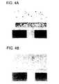
- FIGS. 4 (A) and 4 (B)are photographs of contact holes in TFTs
- FIG. 5 (A)is a schematic view illustrating the contact hole shown in FIG. 4 (A);
- FIG. 5 (B)is a schematic view illustrating the contact hole shown in FIG. 4 (B);
- FIG. 6is a schematic cross section of a device comprising a plurality of TFTs according to the invention, the TFTs being formed on a substrate;
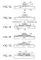
- FIGS. 7 (A) to 7 (H)are cross sections of a TFT according to the invention, illustrating the sequence in which the TFT is fabricated.
- FIGS. 8 (A) to 8 (C)are cross sections of TFTs according to the invention, illustrating the contacts of the source or drain.
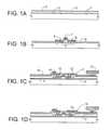
- Example 1is shown in FIGS. 1, (A)-(D), and 2 , (A)-(B).
- FIGS. 1, (A)-(D)illustrate the sequence in which an electronic circuit having TFTs is fabricated. Description of conventional steps is omitted.
- silicon oxidewas deposited as a silicon oxide film 2 forming a base film on a glass substrate 1 made of Corning 7059.
- An amorphous silicon film 3having a thickness of 500 to 1500 ⁇ , preferably 500 to 750 ⁇ , was formed on the silicon oxide film 2 .
- a protective layer 4was formed on the amorphous silicon film 3 .
- the laminatewas annealed at 450 to 600° C. for 12 to 48 hours to crystallize the amorphous silicon film. Of course, laser annealing or other similar means can be used for the crystallization (FIG. 1 (A)).
- the silicon filmwas photolithographically patterned into island-shaped semiconductor regions 5 .
- a silicon oxide film 6having a thickness of 500 to 1500 ⁇ , preferably 800 to 1000 ⁇ , was formed on the semiconductor regions 5 to form a gate oxide film.
- gate interconnects and electrodes 7were fabricated from aluminum.
- the aluminum interconnects and electrodes 7were anodized to form an aluminum oxide coating around the interconnects and electrodes 7 .
- This technique which makes use of anodization for top-gate TFTs in this wayis described in Japanese Patent application Ser. No. 38637/1992, filed Jan. 24, 1992.
- the gate electrodescan be made of silicon, titanium, tantalum, tungsten, molybdenum, or other material.
- an impurity such as phosphoruswas implanted by plasma doping or other method to form doped silicon regions 8 aligned with the gate electrodes 7 .
- the doped regions 8were recrystallized by thermal annealing, laser annealing, or other method to form source and drain regions of TFTs (FIG. 1 (B)).
- silicon oxidewas deposited as an interlayer insulator 9 .
- a conductive transparent oxidesuch as ITO (indium tin oxide) was deposited.
- the ITO filmwas photolithographically patterned into pixel electrodes 10 of an active-matrix liquid crystal display. Contact holes were formed in the interlayer insulator 9 to expose parts of the doped regions, or the source and drain regions.
- a first layer consisting mainly of titanium and nitrogenwas formed by sputtering. Also, a second layer made of aluminum was formed by sputtering in the manner described below.
- a target made of titaniumwas placed in a sputter chamber. Films were formed within argon ambient. The sputtering pressure was 1 to 10 mtorr. First, a layer having titanium as its main. constituent but containing little nitrogen was formed up to a thickness of 50 to 500 ⁇ . Besides argon, nitrogen was introduced into the sputter chamber. Within this ambient, a film was formed by sputtering. As a result, a layer of substantially stoichiometric titanium nitride and having a thickness of 200 to 1000 ⁇ was formed. At this time, the percentage of nitrogen in the sputtering ambient was in excess of 40%.
- the deposition rate by sputteringis affected greatly by the partial pressure of the nitrogen as well as by the sputtering pressure.
- the deposition rate within an ambient consisting only of argonis generally 3 to 5 times as high as the deposition rate within an ambient containing more than 20% nitrogen.
- ammonia, hydradine, or other substancecan be used instead of nitrogen.
- the resistivity of the produced filmvaries, depending on the partial pressure of nitrogen during sputtering. Since the film is used to form conductive interconnects, a lower resistivity is desired.
- an optimum partial pressure of nitrogenis adopted.
- an ambient containing 100% nitrogenproduces a lower resistivity than the resistivity obtained within an ambient containing 40% nitrogen. Typical resistivities were between 50 and 300 ⁇ cm.
- first layer 11aluminum was sputtered to form a second layer 12 containing 1% silicon.
- the thickness of this second layerwas 2000 to 5000 ⁇ . These layers were photolithographically patterned. More specifically, the second layer of aluminum was etched with an etchant such as a mixture acid of phosphoric acid, acetic acid, and nitric acid. Subsequently, the first layer was etched with buffered hydrofluoric acid or nitrous acid while leaving behind the photoresist on the aluminum film. At this time, the interlayer insulator was deteriorated by overetching.
- an etchantsuch as a mixture acid of phosphoric acid, acetic acid, and nitric acid.
- the etching processmight also be carried out by etching the first layer with a mixture of aqueous solution of hydrogen peroxide (H 2 O 2 ) and aqueous ammonia (NH 3 OH), using the aluminum layer selectively left first as a mask.
- the interlayer insulatorwas not affected.
- organic materialssuch as the photoresist were oxidized.
- the above-described etching stepcan be a dry etching process. If carbon tetrachloride (CCl 4 ) is used as an etching gas, the second and first layers can be continuously etched without adversely affecting the silicon oxide. In this way, conductive interconnects extending from the doped regions were formed. Then, the laminate was annealed at 300° C. within an ambient of hydrogen, thus completing TFTs.
- CCl 4carbon tetrachloride
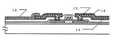
- FIG. 2 (A)shows the manner in which conductive interconnects 19 for connection with the outside extend from an integrated circuit 18 toward substrate peripheral portions, the circuit 18 being formed on a substrate 17 .
- This electronic circuitmay sometimes make electrical contact by mechanical means such as contact fixtures (e.g., sockets) in regions 20 surrounded by the broken line.
- circuits 22 - 24activate an active-matrix region 25 on a substrate 21 .
- electrical contactsare made in regions 27 surrounded by the broken lines. Connections made by wire bonding function permanently and are highly reliable. However, considerable labor is needed to fabricate the connections. Especially, this method is not suited for connection of numerous terminals. Therefore, use of mechanical contacts may sometimes be more advantageous.
- the surfaces of the conductive interconnects at the contactsbe sufficiently strong and that the underlying layer adhere well to the conductive interconnects.
- Aluminumis not suitable for these purposes.
- a material consisting mainly of titaniumadheres well to silicon, silicon oxide, aluminum, and other similar materials.
- the hardness of the coating of this materialis high. Hence, this material is adequate.
- nitrogenbe not contained at all.
- a maximum amount of nitrogen up to its stoichiometric ratiocan be contained.
- the first layer 11only the contacts were etched to expose the second layer.
- those portions of the first layer which were in contact with the second layerwere made of stoichiometric titanium nitride.
- Contact fixtures 13were pressed against the exposed portions of the titanium nitride to form contacts (FIG. 1 (C)).
- a second layer 15is formed on a first layer 14 .
- a third layer 16 of titanium nitrideis formed on the second layer 15 .
- Contact fixturesmay be brought into contact with this third layer. In this case, it is not necessary to partially etch the second layer as shown in FIG. 1 (C). Hence, the patterning step can be omitted.
- a layer consisting mainly of nitrogen and titanium according to the present inventionis first photolithographically patterned into conductive interconnects, and then an ITO film is formed.
- the ITO filmis made of a material consisting principally of nitrogen and titanium. Consequently, good contacts can be obtained.
- the material of the filmis not restricted to ITO. Rather, various other conductive oxides may also be used.
- V D -I D characteristic of the TFTs obtained in this wayis shown as curve a in FIG. 3 .
- the V D -I D characteristic of TFTs having conventional Al/Si contactsis shown as curve b in FIG. 3.
- such abnormalityis not observed on the curve a of the TFTs manufactured according to the present invention, and normal MOS FET characteristics are exhibited.
- FIGS. 4 (A) and 4 (B)are photographs demonstrating that alloying (i.e., formation of a silicide) of the materials of the conductive interconnects extending from the TFTs, i.e., aluminum, with the N-type silicon in the source and drain regions is suppressed under the same conditions as in Example 1.
- the regions shown in the photographs of FIGS. 4 (A) and 4 (B)are schematically shown in FIGS. 5 (A) and 5 (B), respectively.
- a rectangular region seen at the center of each photographis a contact hole.
- the laminatewas annealed at 300° C. for 30 minutes. Where no titanium nitride existed between the silicon and the aluminum as shown in FIG. 4 (A), a large amount of silicide (specks) was produced at the contacts. Where a film of titanium nitride having a thickness of 1000 ⁇ existed as shown in FIG. 4 (B), any deterioration was not observed at all.
- Conventional stepsare not described herein.
- silicon oxidewas deposited as a silicon oxide base film 2 on a glass substrate 1 .
- An amorphous silicon film 3having a thickness of 100 to 1500 ⁇ , preferably 100 to 750 ⁇ , was formed on the silicon oxide film 2 .
- a protective layer 4was formed on the amorphous silicon film 3 .
- the laminatewas annealed at 450 to 600° C. for 12 to 48 hours to crystallize the amorphous silicon film. Of course, laser annealing or other similar means can also be used for the crystallization (FIG. 1 (A)).
- the silicon filmwas photolithographically patterned into island-shaped semiconductor regions 5 .
- a silicon oxide film 6having a thickness of 500 to 1500 ⁇ , preferably 800 to 1000 ⁇ , was formed on the semiconductor regions 5 to form a gate oxide film.
- gate interconnects and electrodes 7were fabricated from aluminum.
- the aluminum interconnects and electrodes 7were anodized to form an aluminum oxide coating around the interconnects and electrodes 7 .
- an impuritysuch as phosphorus was introduced by ion implantation or other method to form doped silicon regions 8 aligned with the gate electrodes 7 .
- the dose, the accelerating voltage, and the thickness of the gate oxide filmwere so set that the dose was 0.8 to 4 ⁇ 10 15 /cm 2 and that the dopant density was 1 ⁇ 10 19 to 1 ⁇ 10 21 /cm 3 .
- the doped regions 8were recrystallized by thermal annealing, laser annealing, or other method to form source and drain regions of TFTs (FIG. 1 (B)).
- silicon oxidewas deposited as an interlayer insulator 9 , followed by deposition of ITO.
- the ITO filmwas photolithographically patterned into pixel electrodes 10 of an active-matrix liquid crystal display.
- Contact holeswere formed in the interlayer insulator 9 to expose parts of the doped regions, or the source and drain regions.
- a first layerconsisting mainly of titanium and nitrogen was formed by sputtering.
- a second layer made of aluminumwas formed by sputtering in the manner described below.
- a target made of titaniumwas placed in a sputter chamber. Films were formed within an ambient consisting of argon and nitrogen. The ratio of the partial pressure of the argon to the partial pressure of the nitrogen was less than 0.3, for example 0.25. The sputtering pressure was 3 mtorr. A DC current of 4.5 A was passed. The flow rate of the argon was 24 SCCM. The flow rate of the nitrogen was 6 SCCM. The first layer had a lower layer containing less nitrogen, the lower layer having a thickness of 100 ⁇ . The film formed in this way showed sufficiently small contact resistance with the silicon and ITO.
- the percentage of the ambient within the sputter chamberwas increased such that the ratio of the partial pressure of the argon to the partial pressure of the nitrogen was in excess of0.3, for example 1.
- a filmwas formed by sputtering.
- the sputtering pressure and the DC currentwere maintained at 3 mtorr and 4.5 A, respectively.
- the flow rates of the argon and the nitrogenwere set to 15 SCCM.
- an upper layer (having a thickness of 900 ⁇ ) of the first layerwas formed.
- the film formed in this mannershowed a large contact resistance with the silicon and so could not be used as contacts. However, this film could be patterned into conductive interconnections without difficulty in the present example.
- the deposition rate by sputteringis affected greatly by the partial pressure of the nitrogen as well as by the sputtering pressure.
- the deposition ratewas 100 to 120 ⁇ /min.
- the deposition ratewas 30 to 40 ⁇ /min.
- the first layer 11After forming the first layer 11 in this way, aluminum was sputtered to form a second layer 12 containing 1% silicon. The thickness of this second layer was 2000 to 5000 ⁇ . These layers were photolithographically patterned. More specifically, the second layer of aluminum was etched with an etchant such as a mixture acid of phosphoric acid, acetic acid, and nitric acid. Subsequently, the first layer was etched with a mixture liquid of aqueous solution of hydrogen peroxide (H 2 O 2 ) and aqueous ammonia (NH 3 OH) while leaving behind the photoresist on the aluminum film. Since this etchant oxidizes organic substances, it follows that a final cleaning of organic substances is simultaneously done.
- an etchantsuch as a mixture acid of phosphoric acid, acetic acid, and nitric acid.
- H 2 O 2hydrogen peroxide
- NH 3 OHaqueous ammonia
- silicon oxidewas deposited as a silicon oxide film 202 on a glass substrate 201 made of Corning 7059.
- the silicon oxide filmformed a base film and had a thickness of 1000 to 3000 ⁇ .
- the substratemeasured 300 mm ⁇ 400 mm or 100 mm ⁇ 100 mm.
- sputteringwas effected within oxygen ambient.
- TEOSmay be decomposed and deposited by plasma CVD.
- amorphous siliconwas deposited as a film having a thickness of 300 to 5000 ⁇ , preferably 500 to 1000 ⁇ , by plasma CVD or LPCVD. This film was allowed to stand within an oxidizing ambient at 550 to 600° C. for 24 hours to crystallize the film. This step may also be carried out by laser irradiation.
- the crystallized silicon filmwas photolithographically patterned into island-shaped regions 203 .
- a silicon oxide film 104 having a thickness of 700 to 1500 ⁇was formed by sputtering techniques.
- An aluminum film having a thickness of 1000 ⁇ to 3 ⁇ mwas then formed by electron-beam evaporation or sputtering.
- This aluminum filmcontained 1% by weight of silicon or 0.1 to 0.3% by weight of scandium.
- the gate electrodes 205were anodized by passing an electric current through an electrolytic solution to form an anodic oxide film 206 having a thickness of 3000 to 6000 ⁇ , for example 5000 ⁇ .
- the anodization stepwas carried out, using an acidic solution of 3 to 20% of citric acid, nitric acid, phosphoric acid, chromic acid, sulfuric acid, or other acid, and by applying a constant voltage of 10 to 30 V to the gate electrodes.
- a voltage of 10 Vwas applied to the gate electrodes in oxalic acid at 30° C. for 20 to 40 minutes for anodic oxidation.
- the thickness of the anodic oxide filmwas controlled by the anodization time (FIG. 7 (B)).
- the silicon oxide film 104was etched by dry etching techniques. In this etching step, either plasma mode of isotropic etching or reactive ion etching mode of anisotropic etching can be used. However, it is important that the active layer be etched not deeply by setting large the selection ratio of the silicon to the silicon oxide. For example, if CF 4 is used as an etching gas, the anodic oxide film is not etched; only the silicon oxide film 104 is etched. The silicon oxide film 204 located under the porous anodic oxide film 206 was not etched but left behind (FIG. 7 (C)).
- the porous anodic oxide film 206was etched away. Then, using the gate electrode portions 205 and 207 and the gate-insulating film 204 as masks, an impurity was implanted by ion doping to form low-resistivity doped regions 208 , 211 and high-resistivity doped regions 209 , 210 . The dose was 1 to 5 ⁇ 10 14 /cm 2 . The accelerating voltage was 39 to 90 kV. Phosphorus was used as the impurity (FIG. 7 (E)).
- An appropriate metalsuch as titanium, nickel, molybdenum, tungsten, platinum, or palladium was sputtered over the whole surface.
- a titanium film 212 having a thickness of 50 to 500 ⁇was formed over the whole surface.
- the metal film, the titanium film 212 in this examplewas in intimate contact with the low-resistivity doped regions 208 and 211 (FIG. 7 (F)).
- Laser radiation emitted from a KrF excimer laser having a wavelength of 248 nm and a pulse width of 20 nsecwas illuminated to activate the implanted impurity and to cause the metal film, or the titanium film, to react with the active layer, thus forming regions 213 and 214 of a metal silicide, or titanium silicide.
- the energy density of the laser radiationwas 200 to 400 mJ/cm 2 , preferably 250 to 300 mJ/cm 2 .
- an excimer laserwas employed as described above.
- the used laseris a pulsed laser. If a CW laser is used, the illumination time is long and so the illuminated object expands due to heat. As a result, the object may peel off.
- Usable pulsed lasersinclude infrared lasers such as an Nd:YAG laser (preferably Q-switched laser), visible light lasers such as those utilizing second-harmonic generation, and various UV lasers using excimers such as KrF, XeCl, and ArF.
- Nd:YAG laserpreferably Q-switched laser
- visible light laserssuch as those utilizing second-harmonic generation
- various UV lasers using excimerssuch as KrF, XeCl, and ArF.
- the laser lightmay also be illuminated from the side of the substrate. In this case, such laser light which is transmitted through the underlying silicon semiconductor layer is required to be selected.
- the annealcan be a lamp anneal using illumination of visible light or near infrared light. Where a lamp anneal is conducted, light is illuminated in such a way that the surface of the illuminated object reaches about 600 to 1000° C. Where the temperature is 600° C., the illumination is continued for several minutes. Where the temperature is 1000° C., the illumination is carried out for tens of seconds.
- An anneal using infrared lightsuch as infrared light of 1.2 ⁇ m is quite advantageous for the following reasons.
- the near infrared lightis absorbed selectively by the silicon semiconductor layer and, therefore, the glass substrate is not heated very much. By setting each illumination time short, the substrate is heated to a less extent.
- the titanium filmwas etched by an etchant consisting of hydrogen peroxide, ammonia, and water at a rate of 5:2:2.
- the exposed layer and those portions of the titanium layer which were not contactede.g., the titanium film existing on the gate-insulating film 204 and on the anodic oxide film 207 ) were left in metal state. These portions could be removed by this etching. Since none of the titanium nitride films 213 and 214 were etched, they could be left behind (FIG. 7 (G)).
- a silicon oxide film having a thickness of 2000 ⁇ to 1 ⁇ m (e.g., 3000 ⁇ )was formed as an interlayer insulator 217 over the whole surface by CVD.
- Contact holeswere formed in the source and drain electrodes of the TFTs.
- Aluminum interconnects and electrodes 218 and 219 having thicknesses of 200 ⁇ to 1 ⁇ m (e.g., 5000 ⁇ )were formed.
- the portions with which the aluminum interconnects were in contactwere made of titanium silicide. The stability at the interface with the aluminum is improved over the case of silicon. Hence, reliable contacts were obtained.
- the reliabilitycould be improved further.
- the sheet resistance of the silicide regionswas 10 to 50 ⁇ /cm 2 .
- the sheet resistance of the high-resistivity regions 209 and 210was 10 to 100 k ⁇ /cm 2 .
- TFTswhich had good frequency characteristics and suffered from less hot carrier deterioration at high drain voltages could be fabricated.
- the low-resistivity doped region 211could be made substantially coincident with the metal suicide regions.
- FIG. 6illustrates an example of fabrication of plural TFTs on a substrate, by the method illustrated in FIGS. 7, (A)-(H).
- three thin-film transistors TFT 1 -TFT 3were formed.
- the TFT 1 and TFT 2were used as driver TFTs and took the form of CMOS devices.
- these TFTswere built as inverters.
- the TFT 3was used as a pixel TFT.
- An anodic oxide film 507had a large value of 2000 ⁇ and took an offset state, thus suppressing leakage current.
- One of the source/drain electrodes of the TFT 3was connected with the pixel electrode 508 of ITO. In order that the anodic oxide films had different thicknesses, they were separated to permit the voltages applied to the gate electrodes of the TFTs to be controlled independently.
- the TFT 1 and TFT 3were n-channel thin-film transistors, while the TFT 2 was a p-channel thin-film transistor.
- the step for forming the titanium filmwas carried out after the ion doping step. This sequence may be reversed. In this case, since the titanium film coats the whole underlying layer when ions are illuminated, abnormal charging, or charge-up, which would be produced on the substrate, is effectively prevented.
- a laser annealing stepis carried out. Then, a titanium film is formed, and a titanium silicide film is formed by laser illumination or thermal annealing.
- the contacts of the source or drain electrodes of the novel TFTsmay take the structure shown in FIGS. 8 (A)- 8 (C). Shown in these figures are a glass substrate 1 , an insulating film 6 , a source or drain 8 , an interlayer insulating film 9 , a titanium silicide region 301 , a titanium nitride layer 302 , an aluminum layer 303 , a titanium nitride layer 304 , a titanium layer 305 , and a titanium nitride layer 306 .
- thin source, drain, or other doped regions, of TFTscan have good contacts, which are highly reliable and hence effective in enhancing the reliability of the whole electronic circuit. In this way, the invention is industrially advantageous.
Landscapes
- Physics & Mathematics (AREA)
- Condensed Matter Physics & Semiconductors (AREA)
- General Physics & Mathematics (AREA)
- Engineering & Computer Science (AREA)
- Computer Hardware Design (AREA)
- Microelectronics & Electronic Packaging (AREA)
- Power Engineering (AREA)
- Thin Film Transistor (AREA)
- Internal Circuitry In Semiconductor Integrated Circuit Devices (AREA)
- Liquid Crystal (AREA)
- Electrodes Of Semiconductors (AREA)
Abstract
Description
This application is a Divisional application of Ser. No. 09/703,594, filed Nov. 2, 2000, now U.S. Pat. No. 6,448,612 which is a Divisional application of Ser. No. 09/382,674, filed Aug. 25, 1999, now U.S. Pat. No. 6,166,414, which is a Divisional application of Ser. No. 09/041,702, filed Mar. 13, 1998, now U.S. Pat. No. 6,031,290, which is a Divisional application of Ser. No. 08/636,917, filed Apr. 24, 1996, now U.S. Pat. No. 5,804,878, which is a Continuation application of Ser. No. 08/162,357, filed Dec. 7, 1993, now abandoned.
The present invention relates to an electronic circuit which is formed on an insulating substrate and has a thin semiconductor layer of silicon, for example, forming thin-film transistors, the thin semiconductor layer being required to be connected with conductive interconnects.
Conventional thin-film devices such as insulated-gate FETs use a thin semiconductor film of silicon as an active layer. This layer is about 1500 Å thick. Therefore, where electrodes should be formed on this thin semiconductor film, satisfactory contacts can be made by bringing a metal such as aluminum into direct and intimate contact with the film, in the same way as in the prior art IC fabrication techniques. In these contacts, a silicide such as aluminum silicide is usually formed by a chemical reaction between the aluminum and the semiconductor component such as silicon. Since the semiconductor layer is sufficiently thicker than the silicide layer, no problems take place.
However, researches conducted recently have demonstrated that if the thickness of the active layer is decreased below 1500 Å, for example, between about 100 to 750 Å, then the characteristics of the TFTs are improved. Where electrodes should be formed on such a thin semiconductor layer, or an active layer, it has not been possible to make good contacts by the prior art techniques, because the thickness of the silicide layer grows almost up to the thickness of the semiconductor layer, thus severely deteriorating the electrical characteristics of the contacts. When a stress such as a voltage is kept applied to the contacts for a long time, the contacts deteriorate seriously.
In order to improve the characteristics of the TFTs, thermal treatment effected below 400° C., typically 200-350° C., within hydrogen ambient is needed after formation of the electrodes on the semiconductor layer. Where the thickness of the semiconductor layer of the TFTs is less than 1500 Å, the thermal processing greatly promotes growth of the silicide, leading to deterioration of the characteristics of the TFTs.
It is an object of the present invention to provide a reliable electronic circuit having a semiconductor layer, conductive interconnects, and good contacts between the semiconductor layer and the interconnects, the contacts being capable of withstanding thermal processing performed at or above 300° C.
The present invention resides in an electronic circuit which is formed on an insulating substrate and has a semiconductor layer consisting mainly of silicon, the thickness of the semiconductor layer being less than 1500 Å, preferably between 100 Å and 750 Å. For example, the invention is applicable to an electronic circuit having TFTs each provided with an active layer having a thickness less than 1500 Å. The effects of the present invention become conspicuous as the thickness of the semiconductor layer decreases.
In a first embodiment of the invention, the above-described semiconductor layer in the form of a thin film is either in intimate contact with the top surface of the insulating substrate as made of glass or formed over this substrate via some insulating film. A first layer consisting principally of titanium and nitrogen is partially or totally in intimate contact with the semiconductor layer. A second layer consisting principally of aluminum is formed on the top surface of the first layer. The first and second layers are photolithographically patterned into conductive interconnects. The bottom surface of the second layer is substantially totally in intimate contact with the first layer. It is possible to form a third layer consisting mainly of titanium and nitrogen on the second layer.
In another embodiment of the invention, the above-described semiconductor layer in the form of a thin film is either in intimate contact with the insulating substrate as made of glass or formed over this substrate via some insulating film. A first layer containing both titanium and silicon is partially or totally in intimate contact with the semiconductor layer. A second layer consisting chiefly of titanium and nitrogen is in intimate contact with the top surface of the first layer. A third layer consisting principally of aluminum is formed on the top surface of the second layer. The first through third layers are photolithographically patterned into conductive interconnects. Of course, other layer may be formed on the third layer.
In a further embodiment of the invention, the above-described semiconductor layer in the form of a thin film is either in intimate contact with the insulating substrate as made of glass or formed over this substrate via some insulating film. A first layer containing both titanium and silicon as main constituents is partially or totally in intimate contact with the semiconductor layer. A second layer consisting chiefly of titanium and nitrogen is in intimate contact with the top surface of the first layer. A third layer consisting principally of aluminum is formed on the top surface of the second layer. The first through third layers are photolithographically patterned into conductive interconnects. This embodiment is characterized in that the ratio of the titanium to the nitrogen in the first layer is greater than the titanium/nitrogen ratio of the second layer.
In any structure of these embodiments, the portions of the thin semiconductor film with which the first layer is in intimate contact show an N- or P-type conductivity. Preferably, the dose in these portions is 1×10¹⁹to 1×10²/cm20. The impurity may be introduced by a well-known ion implantation method or plasma doping method. Where such impurity ions are accelerated to a high energy and introduced, the dose is preferably between 0.8×10¹⁵and 1×10¹⁷/cm2. Also, a laser doping method using laser irradiation within an ambient of an impurity gas may be utilized. This method is described in Japanese Patent application Ser. No. 283981/1991, filed Oct. 4, 1991, and No. 290719/1991, filed Oct. 8, 1991. Preferably, the sheet resistance of these portions is less than 1 kΩ/cm2.
Elements which can be added to the semiconductor layer are phosphorus, boron, arsenic, and others. Those portions of the semiconductor layer which are in contact with the conductive interconnects may be parts of doped regions such as the source and drain regions of the TFTs. Preferably, the sheet resistance of the semiconductor layer is less than 500 Ω/.
A silicon oxide layer may be in intimate contact with the bottom surface of the thin semiconductor layer. In this structure, the silicon oxide film may contain the same impurity as the impurity contained in the semiconductor layer.
In the first layer of the above-described first embodiment, the ratio of the titanium to the nitrogen contained as main constituents may differ according to the thickness. Besides titanium and nitrogen, other elements such as silicon and oxygen can be contained as main constituents. For example, that portion of the first layer which is close to the semiconductor layer may consist principally of titanium and silicon. That portion of the first layer which is close to the second layer may consist mainly of titanium and nitrogen. For instance, the ratio of nitrogen to titanium may be set close to a stoichiometric ratio (exceeding 0.8). In the intermediate region, the constituents may be made to vary continuously.
Generally, a stoichiometric material (titanium nitride) containing nitrogen and titanium has excellent barrier characteristics and prevents diffusion of aluminum and silicon. However, the material shows a high contact resistance with silicon. Therefore, it is not desired to use such a material directly for formation of contacts. On the other hand, a stoichiometric material (titanium silicide) containing titanium and silicon exhibits a low contact resistance with the semiconductor layer consisting mainly of silicon. This is advantageous to form Ohmic contacts. However, aluminum tends to easily diffuse. For example, the aluminum of the second layer diffuses through the first layer, thus forming aluminum silicide in the semiconductor layer.
The complex layer structure described above has been formed to solve these problems. In particular, that portion which is in contact with the second layer is made of substantially stoichiometric titanium nitride and hence the titanium nitride has excellent barrier characteristics. This prevents the aluminum of the second layer from diffusing into the first layer. The portion in contact with the semiconductor layer is made of substantially stoichiometric titanium silicide. Thus, good Ohmic contacts can be derived.
When a film of titanium silicide is formed, it is not necessary to intentionally add silicon. Titanium reacts with the silicon contained in the semiconductor layer. As a result, titanium silicide is automatically formed. For example, therefore, similar effects can be produced by depositing titanium containing less nitrogen onto the portion close to the semiconductor layer and depositing titanium containing more nitrogen onto the portion close to the second layer.
In either case, when the whole first layer is viewed, it consists mainly of titanium and nitrogen. Preferably, the ratio of nitrogen to titanium in the first layer is 0.5 to 1.2. This material containing titanium and nitrogen as main constituents can make Ohmic contacts with a conductive oxide such as indium tin oxide, zinc oxide, and nickel oxide. Where aluminum and such a conductive oxide together form a junction, a thick layer of aluminum oxide is formed at this junction, and it is impossible to have good contacts. In the prior art techniques, a chromium layer has been formed between aluminum and a conductive oxide. Since the chromium is poisonous, alternative materials have been sought for. Materials used in the present invention and consisting mainly of titanium and nitrogen are excellent also in this respect.
Other objects and features of the invention will appear in the course of the description thereof, which follows.
FIGS.1(A) to1(E) are cross sections of a circuit using TFTs according to the invention, illustrating the sequence in which the circuit is fabricated.
FIG.2(A) is a vertical cross section of an electronic circuit according to the invention;
FIG.2(B) is a top view of another electronic circuit according to the invention;
FIG. 3 is a graph illustrating the characteristic curve a of TFTs fabricated according to the invention, as well as the characteristic curve b of TFTs fabricated by the prior art method;
FIGS.4(A) and4(B) are photographs of contact holes in TFTs;
FIG.5(A) is a schematic view illustrating the contact hole shown in FIG.4(A);
FIG.5(B) is a schematic view illustrating the contact hole shown in FIG.4(B);
FIG. 6 is a schematic cross section of a device comprising a plurality of TFTs according to the invention, the TFTs being formed on a substrate;
FIGS.7(A) to7(H) are cross sections of a TFT according to the invention, illustrating the sequence in which the TFT is fabricated; and
FIGS.8(A) to8(C) are cross sections of TFTs according to the invention, illustrating the contacts of the source or drain.
Example 1 is shown in FIGS. 1, (A)-(D), and2, (A)-(B). FIGS. 1, (A)-(D), illustrate the sequence in which an electronic circuit having TFTs is fabricated. Description of conventional steps is omitted. First, silicon oxide was deposited as asilicon oxide film 2 forming a base film on aglass substrate 1 made of Corning 7059. Anamorphous silicon film 3 having a thickness of 500 to 1500 Å, preferably 500 to 750 Å, was formed on thesilicon oxide film 2. Aprotective layer 4 was formed on theamorphous silicon film 3. The laminate was annealed at 450 to 600° C. for 12 to 48 hours to crystallize the amorphous silicon film. Of course, laser annealing or other similar means can be used for the crystallization (FIG.1(A)).
The silicon film was photolithographically patterned into island-shapedsemiconductor regions 5. Asilicon oxide film 6 having a thickness of 500 to 1500 Å, preferably 800 to 1000 Å, was formed on thesemiconductor regions 5 to form a gate oxide film. Then, gate interconnects andelectrodes 7 were fabricated from aluminum. The aluminum interconnects andelectrodes 7 were anodized to form an aluminum oxide coating around the interconnects andelectrodes 7. This technique which makes use of anodization for top-gate TFTs in this way is described in Japanese Patent application Ser. No. 38637/1992, filed Jan. 24, 1992. Of course, the gate electrodes can be made of silicon, titanium, tantalum, tungsten, molybdenum, or other material. Thereafter, using the gate electrodes as a mask, an impurity such as phosphorus was implanted by plasma doping or other method to form dopedsilicon regions 8 aligned with thegate electrodes 7. Then, thedoped regions 8 were recrystallized by thermal annealing, laser annealing, or other method to form source and drain regions of TFTs (FIG.1(B)).
Then, silicon oxide was deposited as aninterlayer insulator 9. A conductive transparent oxide such as ITO (indium tin oxide) was deposited. The ITO film was photolithographically patterned intopixel electrodes 10 of an active-matrix liquid crystal display. Contact holes were formed in theinterlayer insulator 9 to expose parts of the doped regions, or the source and drain regions. A first layer consisting mainly of titanium and nitrogen was formed by sputtering. Also, a second layer made of aluminum was formed by sputtering in the manner described below.
A target made of titanium was placed in a sputter chamber. Films were formed within argon ambient. The sputtering pressure was 1 to 10 mtorr. First, a layer having titanium as its main. constituent but containing little nitrogen was formed up to a thickness of 50 to 500 Å. Besides argon, nitrogen was introduced into the sputter chamber. Within this ambient, a film was formed by sputtering. As a result, a layer of substantially stoichiometric titanium nitride and having a thickness of 200 to 1000 Å was formed. At this time, the percentage of nitrogen in the sputtering ambient was in excess of 40%. It is to be noted that the deposition rate by sputtering is affected greatly by the partial pressure of the nitrogen as well as by the sputtering pressure. For example, the deposition rate within an ambient consisting only of argon is generally 3 to 5 times as high as the deposition rate within an ambient containing more than 20% nitrogen. With respect to the sputtering ambient, ammonia, hydradine, or other substance can be used instead of nitrogen. It is known that the resistivity of the produced film varies, depending on the partial pressure of nitrogen during sputtering. Since the film is used to form conductive interconnects, a lower resistivity is desired. For this purpose, of course, an optimum partial pressure of nitrogen is adopted. For example, an ambient containing 100% nitrogen produces a lower resistivity than the resistivity obtained within an ambient containing 40% nitrogen. Typical resistivities were between 50 and 300 μΩcm.
In the steps described above, if the titanium layer which was formed first and contained little nitrogen was too thick, reaction with the underlying layer occurred. This made it impossible to obtain good contacts. Our research has demonstrated that if the titanium layer is thinner than the semiconductor layer, then favorable results are obtained.
After forming afirst layer 11 in this way, aluminum was sputtered to form asecond layer 12 containing 1% silicon. The thickness of this second layer was 2000 to 5000 Å. These layers were photolithographically patterned. More specifically, the second layer of aluminum was etched with an etchant such as a mixture acid of phosphoric acid, acetic acid, and nitric acid. Subsequently, the first layer was etched with buffered hydrofluoric acid or nitrous acid while leaving behind the photoresist on the aluminum film. At this time, the interlayer insulator was deteriorated by overetching. The etching process might also be carried out by etching the first layer with a mixture of aqueous solution of hydrogen peroxide (H2O2) and aqueous ammonia (NH3OH), using the aluminum layer selectively left first as a mask. In this case, the interlayer insulator was not affected. However, organic materials such as the photoresist were oxidized.
The above-described etching step can be a dry etching process. If carbon tetrachloride (CCl4) is used as an etching gas, the second and first layers can be continuously etched without adversely affecting the silicon oxide. In this way, conductive interconnects extending from the doped regions were formed. Then, the laminate was annealed at 300° C. within an ambient of hydrogen, thus completing TFTs.
The circuit fabricated in this way had portions which were required to be connected to the outside. FIG.2(A) shows the manner in which conductive interconnects19 for connection with the outside extend from anintegrated circuit 18 toward substrate peripheral portions, thecircuit 18 being formed on asubstrate 17. This electronic circuit may sometimes make electrical contact by mechanical means such as contact fixtures (e.g., sockets) inregions 20 surrounded by the broken line.
In a liquid crystal display as shown in FIG.2(B), circuits22-24 activate an active-matrix region 25 on asubstrate 21. In order to supply electric power and signals to the circuits22-24, electrical contacts are made inregions 27 surrounded by the broken lines. Connections made by wire bonding function permanently and are highly reliable. However, considerable labor is needed to fabricate the connections. Especially, this method is not suited for connection of numerous terminals. Therefore, use of mechanical contacts may sometimes be more advantageous.
In this case, however, it is necessary that the surfaces of the conductive interconnects at the contacts be sufficiently strong and that the underlying layer adhere well to the conductive interconnects. Aluminum is not suitable for these purposes. A material consisting mainly of titanium adheres well to silicon, silicon oxide, aluminum, and other similar materials. Also, the hardness of the coating of this material is high. Hence, this material is adequate. It is possible that nitrogen be not contained at all. Also, a maximum amount of nitrogen up to its stoichiometric ratio can be contained. In the present example, of thefirst layer 11, only the contacts were etched to expose the second layer. In the present example, those portions of the first layer which were in contact with the second layer were made of stoichiometric titanium nitride. Contactfixtures 13 were pressed against the exposed portions of the titanium nitride to form contacts (FIG.1(C)).
Alternatively, as shown in FIG.1(D), asecond layer 15 is formed on afirst layer 14. Athird layer 16 of titanium nitride is formed on thesecond layer 15. Contact fixtures may be brought into contact with this third layer. In this case, it is not necessary to partially etch the second layer as shown in FIG.1(C). Hence, the patterning step can be omitted. Furthermore, as shown in FIG.1(E), a layer consisting mainly of nitrogen and titanium according to the present invention is first photolithographically patterned into conductive interconnects, and then an ITO film is formed. In either case, in the present example, the ITO film is made of a material consisting principally of nitrogen and titanium. Consequently, good contacts can be obtained. The material of the film is not restricted to ITO. Rather, various other conductive oxides may also be used.
The VD-IDcharacteristic of the TFTs obtained in this way is shown as curve a in FIG.3. For reference, the VD-IDcharacteristic of TFTs having conventional Al/Si contacts is shown as curve b in FIG. 3. A kink is observed close to VD=0 on the curve b of the TFTs manufactured by the prior art method. Their contact resistances do not make Ohmic contact. On the other hand, such abnormality is not observed on the curve a of the TFTs manufactured according to the present invention, and normal MOS FET characteristics are exhibited.
FIGS.4(A) and4(B) are photographs demonstrating that alloying (i.e., formation of a silicide) of the materials of the conductive interconnects extending from the TFTs, i.e., aluminum, with the N-type silicon in the source and drain regions is suppressed under the same conditions as in Example 1. The regions shown in the photographs of FIGS.4(A) and4(B) are schematically shown in FIGS.5(A) and5(B), respectively. A rectangular region seen at the center of each photograph is a contact hole. After formation of the contact, the laminate was annealed at 300° C. for 30 minutes. Where no titanium nitride existed between the silicon and the aluminum as shown in FIG.4(A), a large amount of silicide (specks) was produced at the contacts. Where a film of titanium nitride having a thickness of 1000 Å existed as shown in FIG.4(B), any deterioration was not observed at all.
The present example is described by referring to FIG. 1, (A)-(D), which conceptually illustrate the sequence in which an electronic circuit having TFTs is fabricated. Conventional steps are not described herein. First, silicon oxide was deposited as a siliconoxide base film 2 on aglass substrate 1. Anamorphous silicon film 3 having a thickness of 100 to 1500 Å, preferably 100 to 750 Å, was formed on thesilicon oxide film 2. Aprotective layer 4 was formed on theamorphous silicon film 3. The laminate was annealed at 450 to 600° C. for 12 to 48 hours to crystallize the amorphous silicon film. Of course, laser annealing or other similar means can also be used for the crystallization (FIG.1(A)).
The silicon film was photolithographically patterned into island-shapedsemiconductor regions 5. Asilicon oxide film 6 having a thickness of 500 to 1500 Å, preferably 800 to 1000 Å, was formed on thesemiconductor regions 5 to form a gate oxide film. Then, gate interconnects andelectrodes 7 were fabricated from aluminum. The aluminum interconnects andelectrodes 7 were anodized to form an aluminum oxide coating around the interconnects andelectrodes 7. Thereafter, using the gate electrodes as a mask, an impurity such as phosphorus was introduced by ion implantation or other method to form dopedsilicon regions 8 aligned with thegate electrodes 7. The dose, the accelerating voltage, and the thickness of the gate oxide film were so set that the dose was 0.8 to 4×10¹⁵/cm2and that the dopant density was 1×10¹⁹to 1×10²¹/cm3. Then, thedoped regions 8 were recrystallized by thermal annealing, laser annealing, or other method to form source and drain regions of TFTs (FIG.1(B)).
Then, silicon oxide was deposited as aninterlayer insulator 9, followed by deposition of ITO. The ITO film was photolithographically patterned intopixel electrodes 10 of an active-matrix liquid crystal display. Contact holes were formed in theinterlayer insulator 9 to expose parts of the doped regions, or the source and drain regions. A first layer consisting mainly of titanium and nitrogen was formed by sputtering. Also, a second layer made of aluminum was formed by sputtering in the manner described below.
A target made of titanium was placed in a sputter chamber. Films were formed within an ambient consisting of argon and nitrogen. The ratio of the partial pressure of the argon to the partial pressure of the nitrogen was less than 0.3, for example 0.25. The sputtering pressure was 3 mtorr. A DC current of 4.5 A was passed. The flow rate of the argon was 24 SCCM. The flow rate of the nitrogen was 6 SCCM. The first layer had a lower layer containing less nitrogen, the lower layer having a thickness of 100 Å. The film formed in this way showed sufficiently small contact resistance with the silicon and ITO.
Then, the percentage of the ambient within the sputter chamber was increased such that the ratio of the partial pressure of the argon to the partial pressure of the nitrogen was in excess of0.3, for example 1. Within this ambient, a film was formed by sputtering. The sputtering pressure and the DC current were maintained at 3 mtorr and 4.5 A, respectively. The flow rates of the argon and the nitrogen were set to 15 SCCM. By the steps described above, an upper layer (having a thickness of 900 Å) of the first layer was formed. The film formed in this manner showed a large contact resistance with the silicon and so could not be used as contacts. However, this film could be patterned into conductive interconnections without difficulty in the present example. It is to be noted that the deposition rate by sputtering is affected greatly by the partial pressure of the nitrogen as well as by the sputtering pressure. For example, where the ratio of argon to nitrogen was 4:1, the deposition rate was 100 to 120 Å/min. Where the ratio of argon to nitrogen was 1:1, the deposition rate was 30 to 40 Å/min.
After forming thefirst layer 11 in this way, aluminum was sputtered to form asecond layer 12 containing 1% silicon. The thickness of this second layer was 2000 to 5000 Å. These layers were photolithographically patterned. More specifically, the second layer of aluminum was etched with an etchant such as a mixture acid of phosphoric acid, acetic acid, and nitric acid. Subsequently, the first layer was etched with a mixture liquid of aqueous solution of hydrogen peroxide (H2O2) and aqueous ammonia (NH3OH) while leaving behind the photoresist on the aluminum film. Since this etchant oxidizes organic substances, it follows that a final cleaning of organic substances is simultaneously done. In this way, conductive interconnects extending from the doped regions were formed. Then, the laminate was annealed at 300° C. within an ambient of hydrogen, thus completing TFTs. In the present example, of thefirst layer 11, only the contacts were etched, thus exposing the second layer. Contactfixtures 13 were pressed against the exposed portions of the first layer to form contacts (FIG.1(C)).
The present example is shown in FIGS. 7, (A)-(H). First, silicon oxide was deposited as asilicon oxide film 202 on aglass substrate 201 made of Corning 7059. The silicon oxide film formed a base film and had a thickness of 1000 to 3000 Å. The substrate measured 300 mm×400 mm or 100 mm×100 mm. To form this oxide film, sputtering was effected within oxygen ambient. To make mass production more efficient, TEOS may be decomposed and deposited by plasma CVD.
Then, amorphous silicon was deposited as a film having a thickness of 300 to 5000 Å, preferably 500 to 1000 Å, by plasma CVD or LPCVD. This film was allowed to stand within an oxidizing ambient at 550 to 600° C. for 24 hours to crystallize the film. This step may also be carried out by laser irradiation. The crystallized silicon film was photolithographically patterned into island-shapedregions 203. Asilicon oxide film 104 having a thickness of 700 to 1500 Å was formed by sputtering techniques.
An aluminum film having a thickness of 1000 Å to 3 μm was then formed by electron-beam evaporation or sputtering. This aluminum film contained 1% by weight of silicon or 0.1 to 0.3% by weight of scandium. A film of photoresist, such as OFPR800/30 cp prepared by TOKYO OHKA KOGYO CO., LTD., was formed by spin coating. If a film of aluminum oxide having a thickness of 100 to 1000 Å was formed by anodization before the formation of the photoresist film, then the aluminum film adhered well to the photoresist film. Also, leakage of electric current from the photoresist layer was suppressed. This was effective in forming porous anodized oxide in a subsequent anodization step. Thereafter, the photoresist film and the aluminum film were photolithographically patterned and etched to formgate electrodes 205 and a masking film200 (FIG.7(A)).
Thegate electrodes 205 were anodized by passing an electric current through an electrolytic solution to form ananodic oxide film 206 having a thickness of 3000 to 6000 Å, for example 5000 Å. The anodization step was carried out, using an acidic solution of 3 to 20% of citric acid, nitric acid, phosphoric acid, chromic acid, sulfuric acid, or other acid, and by applying a constant voltage of 10 to 30 V to the gate electrodes. In the present example, a voltage of 10 V was applied to the gate electrodes in oxalic acid at 30° C. for 20 to 40 minutes for anodic oxidation. The thickness of the anodic oxide film was controlled by the anodization time (FIG.7(B)).
Subsequently, thesilicon oxide film 104 was etched by dry etching techniques. In this etching step, either plasma mode of isotropic etching or reactive ion etching mode of anisotropic etching can be used. However, it is important that the active layer be etched not deeply by setting large the selection ratio of the silicon to the silicon oxide. For example, if CF4is used as an etching gas, the anodic oxide film is not etched; only thesilicon oxide film 104 is etched. Thesilicon oxide film 204 located under the porousanodic oxide film 206 was not etched but left behind (FIG.7(C)).
An electric current was again supplied to each gate electrode within an electrolytic solution. At this time, ethylene glycol solution containing 3 to 10% tartaric acid, boric acid, or nitric acid was used. When the temperature of the solution was lower than room temperature, or about 10° C., a good oxide film was obtained. In this way, a barrier-typeanodic oxide film 207 was formed on the top and side surfaces of the gate electrodes. The thickness of theanodic oxide film 207 was in proportion to the applied voltage. When the applied voltage was 150 V, the thickness of the formed anodic oxide film was 2000 Å. In the present example, the voltage was increased to 80-150 V. The value of the voltage was determined according to the required thickness of the anodic oxide film207 (FIG.7(D)).
Using the barrier-typeanodic oxide film 207 as a mask, the porousanodic oxide film 206 was etched away. Then, using thegate electrode portions film 204 as masks, an impurity was implanted by ion doping to form low-resistivity dopedregions regions
An appropriate metal such as titanium, nickel, molybdenum, tungsten, platinum, or palladium was sputtered over the whole surface. For instance, atitanium film 212 having a thickness of 50 to 500 Å was formed over the whole surface. As a result, the metal film, thetitanium film 212 in this example, was in intimate contact with the low-resistivity dopedregions 208 and211 (FIG.7(F)).
Laser radiation emitted from a KrF excimer laser having a wavelength of 248 nm and a pulse width of 20 nsec was illuminated to activate the implanted impurity and to cause the metal film, or the titanium film, to react with the active layer, thus formingregions
In the present example, an excimer laser was employed as described above. Of course, other laser can be used. Preferably, the used laser is a pulsed laser. If a CW laser is used, the illumination time is long and so the illuminated object expands due to heat. As a result, the object may peel off.
Usable pulsed lasers include infrared lasers such as an Nd:YAG laser (preferably Q-switched laser), visible light lasers such as those utilizing second-harmonic generation, and various UV lasers using excimers such as KrF, XeCl, and ArF. Where laser light is illuminated from above the metal film, it is necessary that the wavelength of the laser light be so selected that the light is not reflected from the metal film. However, where the metal film is quite thin, almost no problems take place. The laser light may also be illuminated from the side of the substrate. In this case, such laser light which is transmitted through the underlying silicon semiconductor layer is required to be selected.
The anneal can be a lamp anneal using illumination of visible light or near infrared light. Where a lamp anneal is conducted, light is illuminated in such a way that the surface of the illuminated object reaches about 600 to 1000° C. Where the temperature is 600° C., the illumination is continued for several minutes. Where the temperature is 1000° C., the illumination is carried out for tens of seconds. An anneal using infrared light such as infrared light of 1.2 μm is quite advantageous for the following reasons. The near infrared light is absorbed selectively by the silicon semiconductor layer and, therefore, the glass substrate is not heated very much. By setting each illumination time short, the substrate is heated to a less extent.
Then, the titanium film was etched by an etchant consisting of hydrogen peroxide, ammonia, and water at a rate of 5:2:2. The exposed layer and those portions of the titanium layer which were not contacted (e.g., the titanium film existing on the gate-insulatingfilm 204 and on the anodic oxide film207) were left in metal state. These portions could be removed by this etching. Since none of thetitanium nitride films
Finally, as shown in FIG.7(H), a silicon oxide film having a thickness of 2000 Å to 1 μm (e.g., 3000 Å) was formed as aninterlayer insulator 217 over the whole surface by CVD. Contact holes were formed in the source and drain electrodes of the TFTs. Aluminum interconnects andelectrodes aluminum electrodes silicide regions resistivity regions region 211 could be made substantially coincident with the metal suicide regions.
FIG. 6 illustrates an example of fabrication of plural TFTs on a substrate, by the method illustrated in FIGS. 7, (A)-(H). In this example, three thin-film transistors TFT1-TFT3 were formed. The TFT1 and TFT2 were used as driver TFTs and took the form of CMOS devices. In the present example, these TFTs were built as inverters. Oxide layers505 and506 corresponding to theanodic oxide film 207 shown in FIGS. 7, (A)-(H), had a small thickness of 200 to 1000 Å, for example 500 Å. These oxide layers slightly overlapped the underlying layer. The TFT3 was used as a pixel TFT. Ananodic oxide film 507 had a large value of 2000 Å and took an offset state, thus suppressing leakage current. One of the source/drain electrodes of the TFT3 was connected with thepixel electrode 508 of ITO. In order that the anodic oxide films had different thicknesses, they were separated to permit the voltages applied to the gate electrodes of the TFTs to be controlled independently. The TFT1 and TFT3 were n-channel thin-film transistors, while the TFT2 was a p-channel thin-film transistor.
In the present example, the step for forming the titanium film was carried out after the ion doping step. This sequence may be reversed. In this case, since the titanium film coats the whole underlying layer when ions are illuminated, abnormal charging, or charge-up, which would be produced on the substrate, is effectively prevented. As a modified example, after ion doping, a laser annealing step is carried out. Then, a titanium film is formed, and a titanium silicide film is formed by laser illumination or thermal annealing.
The contacts of the source or drain electrodes of the novel TFTs may take the structure shown in FIGS.8(A)-8(C). Shown in these figures are aglass substrate 1, an insulatingfilm 6, a source ordrain 8, aninterlayer insulating film 9, atitanium silicide region 301, atitanium nitride layer 302, analuminum layer 303, atitanium nitride layer 304, atitanium layer 305, and atitanium nitride layer 306.
In the present invention, thin source, drain, or other doped regions, of TFTs can have good contacts, which are highly reliable and hence effective in enhancing the reliability of the whole electronic circuit. In this way, the invention is industrially advantageous.
Claims (106)
1. A display device comprising:
a thin film transistor over a substrate, the thin film transistor comprising a semiconductor layer, and a gate electrode with a gate insulating film interposed therebetween; and
a pixel electrode comprising a conductive oxide film electrically connected to the semiconductor layer through an electrode, the electrode having a laminate structure comprising a first conductive layer in contact with the semiconductor layer, a second conductive layer formed on the first conductive layer, and a third conductive layer formed on the second conductive layer and in contact with the pixel electrode,
wherein the first conductive layer comprises titanium, the second conductive layer comprises aluminum, and the third conductive layer comprises titanium.
2. A display device according toclaim 1 wherein the semiconductor layer comprises crystalline silicon.
3. A display device according toclaim 1 wherein the first conductive layer comprises titanium nitride.
4. A display device according toclaim 1 wherein the second conductive layer comprises aluminum containing 1% silicon.
5. A display device according toclaim 1 wherein the third conductive layer comprises titanium nitride.
6. A display device according toclaim 1 wherein the second conductive layer has a thickness of 2000 Å or more.
7. A display device according toclaim 1 wherein the gate electrode comprises at least one selected from the group consisting of aluminum, silicon, titanium, tantalum, tungsten, and molybdenum.
8. A display device according toclaim 1 wherein the gate electrode is formed over the semiconductor layer.
9. A display device according toclaim 1 wherein the display device is an active matrix type liquid crystal display device.
10. A display device comprising:
a thin film transistor over a substrate, the thin film transistor comprising a semiconductor layer, and a gate electrode with a gate insulating film interposed therebetween; and
a pixel electrode comprising indium tin oxide electrically connected to the semiconductor layer through an electrode, the electrode having a laminate structure comprising a first conductive layer in contact with the semiconductor layer, a second conductive layer formed on the first conductive layer, and a third conductive layer formed on the second conductive layer and in contact with the pixel electrode,
wherein the first conductive layer comprises titanium, the second conductive layer comprises aluminum, and the third conductive layer comprises titanium.
11. A display device according toclaim 10 wherein the semiconductor layer comprises crystalline silicon.
12. A display device according toclaim 10 wherein the first conductive layer comprises titanium nitride.
13. A display device according toclaim 10 wherein the second conductive layer comprises aluminum containing 1% silicon.
14. A display device according toclaim 10 wherein the third conductive layer comprises titanium nitride.
15. A display device according toclaim 10 wherein the second conductive layer has a thickness of 2000 Å or more.
16. A display device according toclaim 10 wherein the gate electrode comprises at least one selected from the group consisting of aluminum, silicon, titanium, tantalum, tungsten, and molybdenum.
17. A display device according toclaim 10 wherein the gate electrode is formed over the semiconductor layer.
18. A display device according toclaim 10 wherein the display device is an active matrix type liquid crystal display device.
19. A display device comprising:
a thin film transistor over a substrate, the thin film transistor comprising a semiconductor layer having a thickness less than 1500 Å, and a gate electrode with a gate insulating film interposed therebetween; and
a pixel electrode comprising a conductive oxide film electrically connected to the semiconductor layer through an electrode, the electrode having a laminate structure comprising a first conductive layer in contact with the semiconductor layer, a second conductive layer formed on the first conductive layer, and a third conductive layer formed on the second conductive layer and in contact with the pixel electrode,
wherein the first conductive layer comprises titanium, the second conductive layer comprises aluminum, and the third conductive layer comprises titanium.
20. A display device according toclaim 19 wherein the semiconductor layer comprises crystalline silicon.
21. A display device according toclaim 19 wherein the first conductive layer comprises titanium nitride.
22. A display device according toclaim 19 wherein the second conductive layer comprises aluminum containing 1% silicon.
23. A display device according toclaim 19 wherein the third conductive layer comprises titanium nitride.
24. A display device according toclaim 19 wherein the second conductive layer has a thickness of 2000 Å or more.
25. A display device according toclaim 19 wherein the gate electrode comprises at least one selected from the group consisting of aluminum, silicon, titanium, tantalum, tungsten, and molybdenum.
26. A display device according toclaim 19 wherein the gate electrode is formed over the semiconductor layer.
27. A display device according toclaim 19 wherein the display device is an active matrix type liquid crystal display device.
28. A display device comprising:
a thin film transistor over a substrate, the thin film transistor comprising a semiconductor layer, and a gate electrode with a gate insulating film interposed therebetween; and
a pixel electrode comprising a conductive oxide film electrically connected to the semiconductor layer through an electrode, the electrode having a laminate structure comprising a first conductive layer in contact with the semiconductor layer, a second conductive layer formed on the first conductive layer, and a third conductive layer formed on the second conductive layer and in contact with the pixel electrode,
wherein the first conductive layer comprises titanium, the second conductive layer comprises aluminum having a thickness of 5000 Å or less, and the third conductive layer comprises titanium.
29. A display device according toclaim 28 wherein the semiconductor layer comprises crystalline silicon.
30. A display device according toclaim 28 wherein the first conductive layer comprises titanium nitride.
31. A display device according toclaim 28 wherein the second conductive layer comprises aluminum containing 1% silicon.
32. A display device according toclaim 28 wherein the third conductive layer comprises titanium nitride.
33. A display device according toclaim 28 wherein the second conductive layer has a thickness of 2000 Å or more.
34. A display device according toclaim 28 wherein the gate electrode comprises at least one selected from the group consisting of aluminum, silicon, titanium, tantalum, tungsten, and molybdenum.
35. A display device according toclaim 28 wherein the gate electrode is formed over the semiconductor layer.
36. A display device according toclaim 28 wherein the display device is an active matrix type liquid crystal display device.
37. A display device comprising:
a thin film transistor over a substrate, the thin film transistor comprising a semiconductor layer having a thickness less than 1500 Å, and a gate electrode with a gate insulating film interposed therebetween; and
a pixel electrode comprising indium tin oxide electrically connected to the semiconductor layer through an electrode, the electrode having a laminate structure comprising a first conductive layer in contact with the semiconductor layer, a second conductive layer formed on the first conductive layer, and a third conductive layer formed on the second conductive layer and in contact with the pixel electrode,
wherein the first conductive layer comprises titanium, the second conductive layer comprises aluminum, and the third conductive layer comprises titanium.
38. A display device according toclaim 37 wherein the semiconductor layer comprises crystalline silicon.
39. A display device according toclaim 37 wherein the first conductive layer comprises titanium nitride.
40. A display device according toclaim 37 wherein the second conductive layer comprises aluminum containing 1% silicon.
41. A display device according toclaim 37 wherein the third conductive layer comprises titanium nitride.
42. A display device according toclaim 37 wherein the second conductive layer has a thickness of 2000 Å or more.
43. A display device according toclaim 37 wherein the gate electrode comprises at least one selected from the group consisting of aluminum, silicon, titanium, tantalum, tungsten, and molybdenum.
44. A display device according toclaim 37 wherein the gate electrode is formed over the semiconductor layer.
45. A display device according toclaim 37 wherein the display device is an active matrix type liquid crystal display device.
46. A display device comprising:
a thin film transistor over a substrate, the thin film transistor comprising a semiconductor layer, and a gate electrode with a gate insulating film interposed therebetween; and
a pixel electrode comprising indium tin oxide electrically connected to the semiconductor layer through an electrode, the electrode having a laminate structure comprising a first conductive layer in contact with the semiconductor layer, a second conductive layer formed on the first conductive layer, and a third conductive layer formed on the second conductive layer and in contact with the pixel electrode,
wherein the first conductive layer comprises titanium, the second conductive layer comprises aluminum having a thickness of 5000 Å or less, and the third conductive layer comprises titanium.
47. A display device according toclaim 46 wherein the semiconductor layer comprises crystalline silicon.
48. A display device according toclaim 46 wherein the first conductive layer comprises titanium nitride.
49. A display device according toclaim 46 wherein the second conductive layer comprises aluminum containing 1% silicon.
50. A display device according toclaim 46 wherein the third conductive layer comprises titanium nitride.
51. A display device according toclaim 46 wherein the second conductive layer has a thickness of 2000 Å or more.
52. A display device according toclaim 46 wherein the gate electrode comprises at least one selected from the group consisting of aluminum, silicon, titanium, tantalum, tungsten, and molybdenum.
53. A display device according toclaim 46 wherein the gate electrode is formed over the semiconductor layer.
54. A display device according toclaim 46 wherein the display device is an active matrix type liquid crystal display device.
55. A display device comprising:
a thin film transistor over a substrate, the thin film transistor comprising a semiconductor layer having a thickness less than 1500 Å, and a gate electrode with a gate insulating film interposed therebetween; and
a pixel electrode comprising a conductive oxide film electrically connected to the semiconductor layer through an electrode, the electrode having a laminate structure comprising a first conductive layer in contact with the semiconductor layer, a second conductive layer formed on the first conductive layer, and a third conductive layer formed on the second conductive layer and in contact with the pixel electrode,
wherein the first conductive layer comprises titanium, the second conductive layer comprises aluminum having a thickness of 5000 Å or less, and the third conductive layer comprises titanium.
56. A display device according toclaim 55 wherein the semiconductor layer comprises crystalline silicon.
57. A display device according toclaim 55 wherein the first conductive layer comprises titanium nitride.
58. A display device according toclaim 55 wherein the second conductive layer comprises aluminum containing 1% silicon.
59. A display device according toclaim 55 wherein the third conductive layer comprises titanium nitride.
60. A display device according toclaim 55 wherein the second conductive layer has a thickness of 2000 Å or more.
61. A display device according toclaim 55 wherein the gate electrode comprises at least one selected from the group consisting of aluminum, silicon, titanium, tantalum, tungsten, and molybdenum.
62. A display device according toclaim 55 wherein the gate electrode is formed over the semiconductor layer.
63. A display device according toclaim 55 wherein the display device is an active matrix type liquid crystal display device.
64. A display device comprising:
a thin film transistor over a substrate, the thin film transistor comprising a semiconductor layer having a thickness less than 1500 Å, and a gate electrode with a gate insulating film interposed therebetween; and
a pixel electrode comprising indium tin oxide electrically connected to the semiconductor layer through an electrode, the electrode having a laminate structure comprising a first conductive layer in contact with the semiconductor layer, a second conductive layer formed on the first conductive layer, and a third conductive layer formed on the second conductive layer and in contact with the pixel electrode,
wherein the first conductive layer comprises titanium, the second conductive layer comprises aluminum having a thickness of 5000 Å or less, and the third conductive layer comprises titanium.
65. A display device according toclaim 64 wherein the semiconductor layer comprises crystalline silicon.
66. A display device according toclaim 64 wherein the first conductive layer comprises titanium nitride.
67. A display device according toclaim 64 wherein the second conductive layer comprises aluminum containing 1% silicon.
68. A display device according toclaim 64 wherein the third conductive layer comprises titanium nitride.
69. A display device according toclaim 64 wherein the second conductive layer has a thickness of 2000 Å or more.
70. A display device according toclaim 64 wherein the gate electrode comprises at least one selected from the group consisting of aluminum, silicon, titanium, tantalum, tungsten, and molybdenum.
71. A display device according toclaim 64 wherein the gate electrode is formed over the semiconductor layer.
72. A display device according toclaim 64 wherein the display device is an active matrix type liquid crystal display device.
73. A display device comprising:
a thin film transistor over a substrate, the thin film transistor comprising a semiconductor region, and a gate electrode with a gate insulating film interposed therebetween; and
a pixel electrode comprising a conductive oxide film electrically connected to the semiconductor region through an electrode, the electrode comprising a first layer in contact with the semiconductor region, a second layer formed on the first layer, and a third layer formed on the second layer and in contact with the pixel electrode,
wherein the first layer comprises titanium, the second layer comprises aluminum, and the third layer comprises titanium.
74. A display device according toclaim 73 , wherein the semiconductor region comprises crystalline silicon.
75. A display device according toclaim 73 wherein the first layer comprises titanium nitride.
76. A display device according toclaim 73 wherein the second layer comprises aluminum containing 1% silicon.
77. A display device according toclaim 73 wherein the third layer comprises titanium nitride.
78. A display device according toclaim 73 wherein the second layer has a thickness of 2000 Å or more.
79. A display device according toclaim 73 wherein the gate electrode comprises at least one selected from the group consisting of aluminum, silicon, titanium, tantalum, tungsten, and molybdenum.
80. A display device according toclaim 73 wherein the gate electrode is formed over the semiconductor region.
81. A display device according toclaim 73 wherein the display device is an active matrix type liquid crystal display device.
82. A display device comprising:
a thin film transistor over a substrate, the thin film transistor comprising a semiconductor region, and a gate electrode with a gate insulating film interposed therebetween; and
a pixel electrode comprising indium tin oxide electrically connected to the semiconductor region through an electrode, the electrode comprising a first layer in contact with the semiconductor region, a second layer formed on the first layer, and a third layer formed on the second layer and in contact with the pixel electrode,
wherein the first layer comprises titanium, the second layer comprises aluminum, and the third layer comprises titanium.
83. A display device according toclaim 82 wherein the semiconductor region comprises crystalline silicon.
84. A display device according toclaim 82 wherein the first layer comprises titanium nitride.
85. A display device according toclaim 82 wherein the second layer comprises aluminum containing 1% silicon.
86. A display device according toclaim 82 wherein the third layer comprises titanium nitride.
87. A display device according toclaim 82 wherein the second layer has a thickness of 2000 Å or more.
88. A display device according toclaim 82 wherein the gate electrode comprised at least one selected from the group consisting of aluminum, silicon, titanium, tantalum, tungsten, and molybdenum.
89. A display device according toclaim 82 wherein the gate electrode is formed over the semiconductor region.
90. A display device according toclaim 82 wherein the display device is an active matrix type liquid crystal display device.
91. A displat device comprising:
a thin film transistor over a substrate, the thin film transistor comprising a source region and a drain region which comprise silicon; and
a pixel electrode comprising a conductive oxide film electricallly connected to one of the source region and the drain region through an electrode, the electrode comprising a first layer in contact with the one of the source region and the drain region, a second layer formed on the first layer, and a third layer formed on the second layer,
wherein the pixel electrode is in contact with an upper surface of the third layer, and
wherein the first layer comprises titanium, the second layer comprises aluminum, and the third layer comprises titanium.
92. A display device according toclaim 91 wherein the source region and the drain region comprise crystalline silicon.
93. A display device according toclaim 91 wherein the first layer comprises titanium nitride.
94. A display device according toclaim 91 wherein the second layer comprises aluminum containing 1% silicon.
95. A display device according toclaim 91 wherein the third layer comprises titanium nitride.
96. A display device according toclaim 91 wherein the second layer has a thickness of 2000 Å or more.
97. A display device according toclaim 91 wherein the thin film transistor is a top gate type thin film transistor.
98. A display device according toclaim 91 wherein the display device is an active matrix type liquid crystal display device.
99. A display device comprising:
a thin film transistor over a substrate, the thin film transistor comprising a source region and a drain region which comprise silicon; and
a pixel electrode comprising indium tin oxide electrically connected to one of the source region and the drain region through an electrode, the electrode comprising a first layer in contact with the one of the source region and the drain region, a second layer formed on the first layer, and a third layer formed on the second layer,
wherein the pixel electrode is in contact with an upper surface of the third layer, and
wherein the first layer comprises titanium, the second layer comprises aluminum, and the third layer comprises titanium.
100. A display device according to cliam99 wherein the source region and the drain region comprise crystalline silicon.
101. A display device according toclaim 99 wherein the first layer comprises titanium nitride.
102. A display device according toclaim 99 wherein the second layer comprises aluminum containing 1% silicon.
103. A display device according toclaim 99 wherein the third layer comprises titanium nitride.
104. A. display device according toclaim 99 wherein the second layer has a thickness of 2000 Å or more.
105. A display device according toclaim 99 wherein the thin film transistor is a top gate type thin film transistor.
106. A display device according toclaim 99 wherein the display device is an active matrix type liquid crystal display device.
Priority Applications (7)
| Application Number | Priority Date | Filing Date | Title |
|---|---|---|---|
| US10/193,162US6608353B2 (en) | 1992-12-09 | 2002-07-12 | Thin film transistor having pixel electrode connected to a laminate structure |
| US10/620,420US7045399B2 (en) | 1992-12-09 | 2003-07-17 | Electronic circuit |
| US10/641,008US7061016B2 (en) | 1992-12-09 | 2003-08-15 | Electronic circuit |
| US11/022,882US7105898B2 (en) | 1992-12-09 | 2004-12-28 | Electronic circuit |
| US11/447,955US7547916B2 (en) | 1992-12-09 | 2006-06-07 | Electronic circuit |
| US12/476,445US7897972B2 (en) | 1992-12-09 | 2009-06-02 | Electronic circuit |
| US13/027,502US8294152B2 (en) | 1992-12-09 | 2011-02-15 | Electronic circuit including pixel electrode comprising conductive film |
Applications Claiming Priority (10)
| Application Number | Priority Date | Filing Date | Title |
|---|---|---|---|
| JP35191692 | 1992-12-09 | ||
| JP4-351916 | 1992-12-09 | ||
| JP02328993AJP3587537B2 (en) | 1992-12-09 | 1993-01-18 | Semiconductor device |
| JP5-23289 | 1993-01-18 | ||
| US16235793A | 1993-12-07 | 1993-12-07 | |
| US08/636,917US5804878A (en) | 1992-12-09 | 1996-04-24 | Electronic circuit |
| US09/041,702US6031290A (en) | 1992-12-09 | 1998-03-13 | Electronic circuit |
| US09/382,674US6166414A (en) | 1992-12-09 | 1999-08-25 | Electronic circuit |
| US09/703,594US6448612B1 (en) | 1992-12-09 | 2000-11-02 | Pixel thin film transistor and a driver circuit for driving the pixel thin film transistor |
| US10/193,162US6608353B2 (en) | 1992-12-09 | 2002-07-12 | Thin film transistor having pixel electrode connected to a laminate structure |
Related Parent Applications (1)
| Application Number | Title | Priority Date | Filing Date |
|---|---|---|---|
| US09/703,594DivisionUS6448612B1 (en) | 1992-12-09 | 2000-11-02 | Pixel thin film transistor and a driver circuit for driving the pixel thin film transistor |
Related Child Applications (2)
| Application Number | Title | Priority Date | Filing Date |
|---|---|---|---|
| US10/620,420DivisionUS7045399B2 (en) | 1992-12-09 | 2003-07-17 | Electronic circuit |
| US10/641,008DivisionUS7061016B2 (en) | 1992-12-09 | 2003-08-15 | Electronic circuit |
Publications (2)
| Publication Number | Publication Date |
|---|---|
| US20020179969A1 US20020179969A1 (en) | 2002-12-05 |
| US6608353B2true US6608353B2 (en) | 2003-08-19 |
Family
ID=26360624
Family Applications (12)
| Application Number | Title | Priority Date | Filing Date |
|---|---|---|---|
| US08/483,049Expired - LifetimeUS5623157A (en) | 1992-12-09 | 1995-06-07 | Semiconductor device having a lead including aluminum |
| US08/636,917Expired - LifetimeUS5804878A (en) | 1992-12-09 | 1996-04-24 | Electronic circuit |
| US09/041,702Expired - LifetimeUS6031290A (en) | 1992-12-09 | 1998-03-13 | Electronic circuit |
| US09/382,674Expired - LifetimeUS6166414A (en) | 1992-12-09 | 1999-08-25 | Electronic circuit |
| US09/703,594Expired - Fee RelatedUS6448612B1 (en) | 1992-12-09 | 2000-11-02 | Pixel thin film transistor and a driver circuit for driving the pixel thin film transistor |
| US10/193,162Expired - Fee RelatedUS6608353B2 (en) | 1992-12-09 | 2002-07-12 | Thin film transistor having pixel electrode connected to a laminate structure |
| US10/620,420Expired - Fee RelatedUS7045399B2 (en) | 1992-12-09 | 2003-07-17 | Electronic circuit |
| US10/641,008Expired - Fee RelatedUS7061016B2 (en) | 1992-12-09 | 2003-08-15 | Electronic circuit |
| US11/022,882Expired - Fee RelatedUS7105898B2 (en) | 1992-12-09 | 2004-12-28 | Electronic circuit |
| US11/447,955Expired - Fee RelatedUS7547916B2 (en) | 1992-12-09 | 2006-06-07 | Electronic circuit |
| US12/476,445Expired - Fee RelatedUS7897972B2 (en) | 1992-12-09 | 2009-06-02 | Electronic circuit |
| US13/027,502Expired - Fee RelatedUS8294152B2 (en) | 1992-12-09 | 2011-02-15 | Electronic circuit including pixel electrode comprising conductive film |
Family Applications Before (5)
| Application Number | Title | Priority Date | Filing Date |
|---|---|---|---|
| US08/483,049Expired - LifetimeUS5623157A (en) | 1992-12-09 | 1995-06-07 | Semiconductor device having a lead including aluminum |
| US08/636,917Expired - LifetimeUS5804878A (en) | 1992-12-09 | 1996-04-24 | Electronic circuit |
| US09/041,702Expired - LifetimeUS6031290A (en) | 1992-12-09 | 1998-03-13 | Electronic circuit |
| US09/382,674Expired - LifetimeUS6166414A (en) | 1992-12-09 | 1999-08-25 | Electronic circuit |
| US09/703,594Expired - Fee RelatedUS6448612B1 (en) | 1992-12-09 | 2000-11-02 | Pixel thin film transistor and a driver circuit for driving the pixel thin film transistor |
Family Applications After (6)
| Application Number | Title | Priority Date | Filing Date |
|---|---|---|---|
| US10/620,420Expired - Fee RelatedUS7045399B2 (en) | 1992-12-09 | 2003-07-17 | Electronic circuit |
| US10/641,008Expired - Fee RelatedUS7061016B2 (en) | 1992-12-09 | 2003-08-15 | Electronic circuit |
| US11/022,882Expired - Fee RelatedUS7105898B2 (en) | 1992-12-09 | 2004-12-28 | Electronic circuit |
| US11/447,955Expired - Fee RelatedUS7547916B2 (en) | 1992-12-09 | 2006-06-07 | Electronic circuit |
| US12/476,445Expired - Fee RelatedUS7897972B2 (en) | 1992-12-09 | 2009-06-02 | Electronic circuit |
| US13/027,502Expired - Fee RelatedUS8294152B2 (en) | 1992-12-09 | 2011-02-15 | Electronic circuit including pixel electrode comprising conductive film |
Country Status (5)
| Country | Link |
|---|---|
| US (12) | US5623157A (en) |
| JP (1) | JP3587537B2 (en) |
| KR (1) | KR0131057B1 (en) |
| CN (8) | CN1664683B (en) |
| TW (1) | TW359891B (en) |
Cited By (36)
| Publication number | Priority date | Publication date | Assignee | Title |
|---|---|---|---|---|
| US20010041392A1 (en)* | 2000-05-12 | 2001-11-15 | Hideomi Suzawa | Semiconductor device and manufacturing method thereof |
| US20020123179A1 (en)* | 1993-01-18 | 2002-09-05 | Semiconductor Energy Laboratory Co., Ltd. | MIS semiconductor device and method of fabricating the same |
| US20030193054A1 (en)* | 2002-04-15 | 2003-10-16 | Semiconductor Energy Laboratory Co., Ltd. | Display device and method of fabricating the same |
| US20030197466A1 (en)* | 2002-04-23 | 2003-10-23 | Semiconductor Energy Laboratory Co., Ltd. | Light emitting device and method of manufacturing the same |
| US20030197178A1 (en)* | 2002-04-23 | 2003-10-23 | Semiconductor Energy Laboratory Co., Ltd. | Semiconductor device and display element using semiconductor device |
| US20030201447A1 (en)* | 2002-04-24 | 2003-10-30 | Semiconductor Energy Laboratory Co., Ltd. | Semiconductor device and method of manufacturing same |
| US20030201716A1 (en)* | 2002-04-26 | 2003-10-30 | Semiconductor Energy Laboratory Co., Ltd. | Light emitting device and manufacturing method of the same |
| US20030227021A1 (en)* | 2002-06-07 | 2003-12-11 | Semiconductor Energy Laboratory Co., Ltd. | Light emitting device and manufacturing method thereof |
| US20030230764A1 (en)* | 2002-05-13 | 2003-12-18 | Semiconductor Energy Laboratory Co., Ltd. | Display device |
| US20040041190A1 (en)* | 1998-02-25 | 2004-03-04 | Semiconductor Engergy Laboratory Co., Ltd. | Projection TV |
| US20040046174A1 (en)* | 1996-06-04 | 2004-03-11 | Semiconductor Energy Laboratory Co., Ltd., A Japan Corporation | Semiconductor integrated circuit and fabrication method thereof |
| US6777763B1 (en) | 1993-10-01 | 2004-08-17 | Semiconductor Energy Laboratory Co., Ltd. | Semiconductor device and method for fabricating the same |
| US20040175860A1 (en)* | 2003-03-07 | 2004-09-09 | Kwangju Institute Of Science And Technology | Method for manufacturing zinc oxide semiconductors |
| US20040183072A1 (en)* | 2003-03-12 | 2004-09-23 | Tae-Sung Kim | Novel conductive elements for thin film transistors used in a flat panel display |
| US6853083B1 (en) | 1995-03-24 | 2005-02-08 | Semiconductor Energy Laboratory Co., Ltd. | Thin film transfer, organic electroluminescence display device and manufacturing method of the same |
| US20050040476A1 (en)* | 1993-10-01 | 2005-02-24 | Semiconductor Energy Laboratory Co., Ltd. | Semiconductor device, and a method for manufacturing the same |
| US20050056934A1 (en)* | 1999-07-22 | 2005-03-17 | Semiconductor Energy Laboratory Co. Ltd. | Wiring and manufacturing method thereof, semiconductor device comprising said wiring, and dry etching method |
| US20050072973A1 (en)* | 2003-03-12 | 2005-04-07 | Tae-Sung Kim | Novel conductive elements for thin film transistors used in a flat panel display |
| US20050073243A1 (en)* | 2002-06-27 | 2005-04-07 | Semiconductor Energy Laboratory Co., Ltd. | Light emitting device and method of manufacturing the same |
| US20050233507A1 (en)* | 2002-04-15 | 2005-10-20 | Semiconductor Energy Laboratory Co., Ltd. | Semiconductor display device and method of manufacturing the same |
| US6958490B2 (en) | 2002-12-27 | 2005-10-25 | Semiconductor Energy Laboratory Co., Ltd. | Light-emitting apparatus |
| US6992332B2 (en) | 2002-05-15 | 2006-01-31 | Semiconductor Energy Laboratory Co., Ltd. | Light emitting device and method for manufacturing the same |
| US20060038176A1 (en)* | 2004-08-20 | 2006-02-23 | Kengo Akimoto | Semiconductor device and manufacturing method thereof |
| US20060086937A1 (en)* | 2002-08-30 | 2006-04-27 | Akiyoshi Fujii | Tft array substrate, liquid crystal display device, manufacturing methods of tft array substrate and liquid crystal display device, and electronic device |
| US20060091397A1 (en)* | 2004-11-04 | 2006-05-04 | Kengo Akimoto | Display device and method for manufacturing the same |
| US20070012923A1 (en)* | 1992-12-09 | 2007-01-18 | Semiconductor Energy Laboratory Co., Ltd. | Electronic circuit |
| US7183614B2 (en) | 1994-07-14 | 2007-02-27 | Semiconductor Energy Laboratory Co., Ltd. | Semiconductor device and method of manufacture thereof |
| US20070278489A1 (en)* | 2002-05-17 | 2007-12-06 | Shunpei Yamazaki | Display device |
| US20080136989A1 (en)* | 2004-09-15 | 2008-06-12 | Semiconductor Energy Laboratory Co., Ltd. | Semiconductor Device |
| US7671369B2 (en) | 2002-04-09 | 2010-03-02 | Semiconductor Energy Laboratory Co., Ltd. | Semiconductor display device |
| US7687809B2 (en) | 1995-01-17 | 2010-03-30 | Semiconductor Energy Laboratory Co., Ltd | Method for producing a semiconductor integrated circuit including a thin film transistor and a capacitor |
| US7915615B2 (en) | 2000-02-22 | 2011-03-29 | Semiconductor Energy Laboratory Co., Ltd. | Semiconductor device and method of manufacturing the same |
| US7955975B2 (en) | 2002-04-09 | 2011-06-07 | Semiconductor Energy Laboratory Co., Ltd. | Semiconductor element and display device using the same |
| US8487315B2 (en) | 2000-04-12 | 2013-07-16 | Semiconductor Energy Laboratory Co., Ltd. | Illumination apparatus |
| US8946011B2 (en) | 2010-09-03 | 2015-02-03 | Semiconductor Energy Laboratory Co., Ltd. | Semiconductor device and manufacturing method thereof |
| US20190280067A1 (en)* | 2018-03-08 | 2019-09-12 | Samsung Display Co., Ltd. | Display device and manufacturing method thereof |
Families Citing this family (179)
| Publication number | Priority date | Publication date | Assignee | Title |
|---|---|---|---|---|
| US5643801A (en)* | 1992-11-06 | 1997-07-01 | Semiconductor Energy Laboratory Co., Ltd. | Laser processing method and alignment |
| US6410374B1 (en) | 1992-12-26 | 2002-06-25 | Semiconductor Energy Laborartory Co., Ltd. | Method of crystallizing a semiconductor layer in a MIS transistor |
| US6544825B1 (en) | 1992-12-26 | 2003-04-08 | Semiconductor Energy Laboratory Co., Ltd. | Method of fabricating a MIS transistor |
| JP2814049B2 (en) | 1993-08-27 | 1998-10-22 | 株式会社半導体エネルギー研究所 | Semiconductor device and manufacturing method thereof |
| TW297142B (en)* | 1993-09-20 | 1997-02-01 | Handotai Energy Kenkyusho Kk | |
| US6133620A (en)* | 1995-05-26 | 2000-10-17 | Semiconductor Energy Laboratory Co., Ltd. | Semiconductor device and process for fabricating the same |
| US5712191A (en)* | 1994-09-16 | 1998-01-27 | Semiconductor Energy Laboratory Co., Ltd. | Method for producing semiconductor device |
| JPH08129360A (en) | 1994-10-31 | 1996-05-21 | Tdk Corp | Electroluminescence display device |
| JP3778456B2 (en) | 1995-02-21 | 2006-05-24 | 株式会社半導体エネルギー研究所 | Method for manufacturing insulated gate thin film semiconductor device |
| US5780908A (en)* | 1995-05-09 | 1998-07-14 | Matsushita Electric Industrial Co., Ltd. | Semiconductor apparatus with tungstein nitride |
| US5972790A (en)* | 1995-06-09 | 1999-10-26 | Tokyo Electron Limited | Method for forming salicides |
| JPH09191111A (en)* | 1995-11-07 | 1997-07-22 | Semiconductor Energy Lab Co Ltd | Semiconductor device and manufacturing method thereof |
| US5985740A (en)* | 1996-01-19 | 1999-11-16 | Semiconductor Energy Laboratory Co., Ltd. | Method of manufacturing a semiconductor device including reduction of a catalyst |
| US6555449B1 (en) | 1996-05-28 | 2003-04-29 | Trustees Of Columbia University In The City Of New York | Methods for producing uniform large-grained and grain boundary location manipulated polycrystalline thin film semiconductors using sequential lateral solidfication |
| US6266110B1 (en)* | 1996-07-30 | 2001-07-24 | Kawasaki Steel Corporation | Semiconductor device reeventing light from entering its substrate transistor and the same for driving reflection type liquid crystal |
| JPH10135475A (en)* | 1996-10-31 | 1998-05-22 | Semiconductor Energy Lab Co Ltd | Semiconductor device and manufacturing method thereof |
| US6088070A (en) | 1997-01-17 | 2000-07-11 | Semiconductor Energy Laboratory Co., Ltd. | Active matrix liquid crystal with capacitor between light blocking film and pixel connecting electrode |
| JP3641342B2 (en)* | 1997-03-07 | 2005-04-20 | Tdk株式会社 | Semiconductor device and organic EL display device |
| TW531684B (en)* | 1997-03-31 | 2003-05-11 | Seiko Epson Corporatoin | Display device and method for manufacturing the same |
| GB9806609D0 (en)* | 1998-03-28 | 1998-05-27 | Philips Electronics Nv | Electronic devices comprising thin-film transistors |
| US5990493A (en)* | 1998-05-14 | 1999-11-23 | Advanced Micro Devices, Inc. | Diamond etch stop rendered conductive by a gas cluster ion beam implant of titanium |
| US6271590B1 (en) | 1998-08-21 | 2001-08-07 | Micron Technology, Inc. | Graded layer for use in semiconductor circuits and method for making same |
| JP3403949B2 (en)* | 1998-09-03 | 2003-05-06 | シャープ株式会社 | Thin film transistor, liquid crystal display device, and method of manufacturing thin film transistor |
| EP1003207B1 (en) | 1998-10-05 | 2016-09-07 | Semiconductor Energy Laboratory Co., Ltd. | Laser irradiation apparatus, laser irradiation method, beam homogenizer, semiconductor device, and method of manufacturing the semiconductor device |
| US6451644B1 (en)* | 1998-11-06 | 2002-09-17 | Advanced Micro Devices, Inc. | Method of providing a gate conductor with high dopant activation |
| US6617644B1 (en) | 1998-11-09 | 2003-09-09 | Semiconductor Energy Laboratory Co., Ltd. | Semiconductor device and method of manufacturing the same |
| US7141821B1 (en) | 1998-11-10 | 2006-11-28 | Semiconductor Energy Laboratory Co., Ltd. | Semiconductor device having an impurity gradient in the impurity regions and method of manufacture |
| US6512271B1 (en)* | 1998-11-16 | 2003-01-28 | Semiconductor Energy Laboratory Co., Ltd. | Semiconductor device |
| US6420758B1 (en)* | 1998-11-17 | 2002-07-16 | Semiconductor Energy Laboratory Co., Ltd. | Semiconductor device having an impurity region overlapping a gate electrode |
| US6909114B1 (en) | 1998-11-17 | 2005-06-21 | Semiconductor Energy Laboratory Co., Ltd. | Semiconductor device having LDD regions |
| US6501098B2 (en)* | 1998-11-25 | 2002-12-31 | Semiconductor Energy Laboratory Co, Ltd. | Semiconductor device |
| US6277679B1 (en) | 1998-11-25 | 2001-08-21 | Semiconductor Energy Laboratory Co., Ltd. | Method of manufacturing thin film transistor |
| US6365917B1 (en) | 1998-11-25 | 2002-04-02 | Semiconductor Energy Laboratory Co., Ltd. | Semiconductor device |
| US7235810B1 (en) | 1998-12-03 | 2007-06-26 | Semiconductor Energy Laboratory Co., Ltd. | Semiconductor device and method of fabricating the same |
| US6469317B1 (en) | 1998-12-18 | 2002-10-22 | Semiconductor Energy Laboratory Co., Ltd. | Semiconductor device and method of fabricating the same |
| US6576924B1 (en)* | 1999-02-12 | 2003-06-10 | Semiconductor Energy Laboratory Co., Ltd. | Semiconductor device having at least a pixel unit and a driver circuit unit over a same substrate |
| US6576926B1 (en)* | 1999-02-23 | 2003-06-10 | Semiconductor Energy Laboratory Co., Ltd. | Semiconductor device and fabrication method thereof |
| JP3362008B2 (en)* | 1999-02-23 | 2003-01-07 | シャープ株式会社 | Liquid crystal display device and manufacturing method thereof |
| US7821065B2 (en)* | 1999-03-02 | 2010-10-26 | Semiconductor Energy Laboratory Co., Ltd. | Semiconductor device comprising a thin film transistor comprising a semiconductor thin film and method of manufacturing the same |
| US6677613B1 (en)* | 1999-03-03 | 2004-01-13 | Semiconductor Energy Laboratory Co., Ltd. | Semiconductor device and method of fabricating the same |
| US6674136B1 (en) | 1999-03-04 | 2004-01-06 | Semiconductor Energy Laboratory Co., Ltd. | Semiconductor device having driver circuit and pixel section provided over same substrate |
| US6531713B1 (en)* | 1999-03-19 | 2003-03-11 | Semiconductor Energy Laboratory Co., Ltd. | Electro-optical device and manufacturing method thereof |
| US6281552B1 (en)* | 1999-03-23 | 2001-08-28 | Semiconductor Energy Laboratory Co., Ltd. | Thin film transistors having ldd regions |
| US6858898B1 (en)* | 1999-03-23 | 2005-02-22 | Semiconductor Energy Laboratory Co., Ltd. | Semiconductor device and method for manufacturing the same |
| TW469484B (en) | 1999-03-26 | 2001-12-21 | Semiconductor Energy Lab | A method for manufacturing an electrooptical device |
| US6346730B1 (en)* | 1999-04-06 | 2002-02-12 | Semiconductor Energy Laboratory Co., Ltd. | Liquid crystal display device having a pixel TFT formed in a display region and a drive circuit formed in the periphery of the display region on the same substrate |
| TW444257B (en) | 1999-04-12 | 2001-07-01 | Semiconductor Energy Lab | Semiconductor device and method for fabricating the same |
| TW518650B (en)* | 1999-04-15 | 2003-01-21 | Semiconductor Energy Lab | Electro-optical device and electronic equipment |
| US6362507B1 (en)* | 1999-04-20 | 2002-03-26 | Semiconductor Energy Laboratory Co., Ltd. | Electro-optical devices in which pixel section and the driver circuit are disposed over the same substrate |
| EP1049167A3 (en) | 1999-04-30 | 2007-10-24 | Sel Semiconductor Energy Laboratory Co., Ltd. | Semiconductor device and manufacturing method thereof |
| US6461899B1 (en)* | 1999-04-30 | 2002-10-08 | Semiconductor Energy Laboratory, Co., Ltd. | Oxynitride laminate “blocking layer” for thin film semiconductor devices |
| US6370502B1 (en)* | 1999-05-27 | 2002-04-09 | America Online, Inc. | Method and system for reduction of quantization-induced block-discontinuities and general purpose audio codec |
| CN1263159C (en)* | 1999-06-02 | 2006-07-05 | 株式会社半导体能源研究所 | Semiconductor device and manufacturing method thereof |
| US6952020B1 (en) | 1999-07-06 | 2005-10-04 | Semiconductor Energy Laboratory Co., Ltd. | Semiconductor device and manufacturing method thereof |
| JP4666723B2 (en) | 1999-07-06 | 2011-04-06 | 株式会社半導体エネルギー研究所 | Method for manufacturing semiconductor device |
| TW490713B (en)* | 1999-07-22 | 2002-06-11 | Semiconductor Energy Lab | Semiconductor device and manufacturing method thereof |
| TW480554B (en) | 1999-07-22 | 2002-03-21 | Semiconductor Energy Lab | Semiconductor device and manufacturing method thereof |
| JP3538084B2 (en)* | 1999-09-17 | 2004-06-14 | 株式会社半導体エネルギー研究所 | Method for manufacturing semiconductor device |
| US6885366B1 (en) | 1999-09-30 | 2005-04-26 | Semiconductor Energy Laboratory Co., Ltd. | Display device |
| US6876145B1 (en) | 1999-09-30 | 2005-04-05 | Semiconductor Energy Laboratory Co., Ltd. | Organic electroluminescent display device |
| JP4562835B2 (en)* | 1999-11-05 | 2010-10-13 | 株式会社半導体エネルギー研究所 | Method for manufacturing semiconductor device |
| US6646287B1 (en)* | 1999-11-19 | 2003-11-11 | Semiconductor Energy Laboratory Co., Ltd. | Semiconductor device with tapered gate and insulating film |
| JP2001175198A (en)* | 1999-12-14 | 2001-06-29 | Semiconductor Energy Lab Co Ltd | Semiconductor device and manufacturing method thereof |
| TW503439B (en)* | 2000-01-21 | 2002-09-21 | United Microelectronics Corp | Combination structure of passive element and logic circuit on silicon on insulator wafer |
| US6825488B2 (en)* | 2000-01-26 | 2004-11-30 | Semiconductor Energy Laboratory Co., Ltd. | Semiconductor device and manufacturing method thereof |
| US6646692B2 (en)* | 2000-01-26 | 2003-11-11 | Semiconductor Energy Laboratory Co., Ltd. | Liquid-crystal display device and method of fabricating the same |
| US6639265B2 (en) | 2000-01-26 | 2003-10-28 | Semiconductor Energy Laboratory Co., Ltd. | Semiconductor device and method of manufacturing the semiconductor device |
| TW494447B (en) | 2000-02-01 | 2002-07-11 | Semiconductor Energy Lab | Semiconductor device and manufacturing method thereof |
| TW521303B (en)* | 2000-02-28 | 2003-02-21 | Semiconductor Energy Lab | Electronic device |
| TW507258B (en)* | 2000-02-29 | 2002-10-21 | Semiconductor Systems Corp | Display device and method for fabricating the same |
| TW495854B (en)* | 2000-03-06 | 2002-07-21 | Semiconductor Energy Lab | Semiconductor device and manufacturing method thereof |
| JP4683688B2 (en) | 2000-03-16 | 2011-05-18 | 株式会社半導体エネルギー研究所 | Method for manufacturing liquid crystal display device |
| US6830993B1 (en) | 2000-03-21 | 2004-12-14 | The Trustees Of Columbia University In The City Of New York | Surface planarization of thin silicon films during and after processing by the sequential lateral solidification method |
| TW513753B (en)* | 2000-03-27 | 2002-12-11 | Semiconductor Energy Lab | Semiconductor display device and manufacturing method thereof |
| DE20006642U1 (en) | 2000-04-11 | 2000-08-17 | Agilent Technologies, Inc. (n.d.Ges.d.Staates Delaware), Palo Alto, Calif. | Optical device |
| US7525165B2 (en) | 2000-04-17 | 2009-04-28 | Semiconductor Energy Laboratory Co., Ltd. | Light emitting device and manufacturing method thereof |
| US6706544B2 (en) | 2000-04-19 | 2004-03-16 | Semiconductor Energy Laboratory Co., Ltd. | Light emitting device and fabricating method thereof |
| US7579203B2 (en) | 2000-04-25 | 2009-08-25 | Semiconductor Energy Laboratory Co., Ltd. | Light emitting device |
| US6580475B2 (en) | 2000-04-27 | 2003-06-17 | Semiconductor Energy Laboratory Co., Ltd. | Semiconductor device and method of fabricating the same |
| US6747289B2 (en) | 2000-04-27 | 2004-06-08 | Semiconductor Energy Laboratory Co., Ltd. | Semiconductor device and method of fabricating thereof |
| TW480576B (en)* | 2000-05-12 | 2002-03-21 | Semiconductor Energy Lab | Semiconductor device and method for manufacturing same |
| US7804552B2 (en)* | 2000-05-12 | 2010-09-28 | Semiconductor Energy Laboratory Co., Ltd. | Electro-optical device with light shielding portion comprising laminated colored layers, electrical equipment having the same, portable telephone having the same |
| US7633471B2 (en)* | 2000-05-12 | 2009-12-15 | Semiconductor Energy Laboratory Co., Ltd. | Light-emitting device and electric appliance |
| TW501282B (en) | 2000-06-07 | 2002-09-01 | Semiconductor Energy Lab | Method of manufacturing semiconductor device |
| US6613620B2 (en) | 2000-07-31 | 2003-09-02 | Semiconductor Energy Laboratory Co., Ltd. | Semiconductor device and method of manufacturing the same |
| JP2002057339A (en)* | 2000-08-10 | 2002-02-22 | Sony Corp | Thin film semiconductor device |
| US6562671B2 (en)* | 2000-09-22 | 2003-05-13 | Semiconductor Energy Laboratory Co., Ltd. | Semiconductor display device and manufacturing method thereof |
| US6509616B2 (en) | 2000-09-29 | 2003-01-21 | Semiconductor Energy Laboratory Co., Ltd. | Semiconductor device and its manufacturing method |
| KR100854834B1 (en) | 2000-10-10 | 2008-08-27 | 더 트러스티스 오브 컬럼비아 유니버시티 인 더 시티 오브 뉴욕 | Method and apparatus for processing thin metal layers |
| JP5046452B2 (en)* | 2000-10-26 | 2012-10-10 | 株式会社半導体エネルギー研究所 | Method for manufacturing semiconductor device |
| JP2002151698A (en) | 2000-11-14 | 2002-05-24 | Semiconductor Energy Lab Co Ltd | Semiconductor device and manufacturing method thereof |
| JP4954366B2 (en) | 2000-11-28 | 2012-06-13 | 株式会社半導体エネルギー研究所 | Method for manufacturing semiconductor device |
| TW525216B (en) | 2000-12-11 | 2003-03-21 | Semiconductor Energy Lab | Semiconductor device, and manufacturing method thereof |
| SG111923A1 (en)* | 2000-12-21 | 2005-06-29 | Semiconductor Energy Lab | Light emitting device and method of manufacturing the same |
| SG160191A1 (en) | 2001-02-28 | 2010-04-29 | Semiconductor Energy Lab | Semiconductor device and manufacturing method thereof |
| SG138468A1 (en)* | 2001-02-28 | 2008-01-28 | Semiconductor Energy Lab | A method of manufacturing a semiconductor device |
| SG116443A1 (en)* | 2001-03-27 | 2005-11-28 | Semiconductor Energy Lab | Wiring and method of manufacturing the same, and wiring board and method of manufacturing the same. |
| JP4926329B2 (en) | 2001-03-27 | 2012-05-09 | 株式会社半導体エネルギー研究所 | Semiconductor device, method for manufacturing the same, and electric appliance |
| KR100437475B1 (en)* | 2001-04-13 | 2004-06-23 | 삼성에스디아이 주식회사 | Method for fabricating display device used in flat display device |
| US6897477B2 (en)* | 2001-06-01 | 2005-05-24 | Semiconductor Energy Laboratory Co., Ltd. | Semiconductor device, manufacturing method thereof, and display device |
| KR100415617B1 (en)* | 2001-12-06 | 2004-01-24 | 엘지.필립스 엘시디 주식회사 | Etchant and method of fabricating metal wiring and thin film transistor using the same |
| JP2003253482A (en)* | 2002-03-01 | 2003-09-10 | Ngk Insulators Ltd | Method for removing titanium film and titanium oxide |
| JP2003330388A (en)* | 2002-05-15 | 2003-11-19 | Semiconductor Energy Lab Co Ltd | Semiconductor device and manufacturing method thereof |
| WO2004017380A2 (en) | 2002-08-19 | 2004-02-26 | The Trustees Of Columbia University In The City Of New York | A single-shot semiconductor processing system and method having various irradiation patterns |
| KR101131040B1 (en) | 2002-08-19 | 2012-03-30 | 더 트러스티스 오브 콜롬비아 유니버시티 인 더 시티 오브 뉴욕 | Process and system for laser crystallization processing of film regions on a substrate to minimize edge areas, and structure of such film regions |
| US7094684B2 (en)* | 2002-09-20 | 2006-08-22 | Semiconductor Energy Laboratory Co., Ltd. | Manufacturing method of semiconductor device |
| TWI338346B (en) | 2002-09-20 | 2011-03-01 | Semiconductor Energy Lab | Display device and manufacturing method thereof |
| WO2004075263A2 (en) | 2003-02-19 | 2004-09-02 | The Trustees Of Columbia University In The City Of New York | System and process for processing a plurality of semiconductor thin films which are crystallized using sequential lateral solidification techniques |
| KR100514181B1 (en)* | 2003-09-03 | 2005-09-13 | 삼성에스디아이 주식회사 | series thin film transistor, active matrix oled using the same and fabrication method of the active matrix oled |
| WO2005029546A2 (en) | 2003-09-16 | 2005-03-31 | The Trustees Of Columbia University In The City Of New York | Method and system for providing a continuous motion sequential lateral solidification for reducing or eliminating artifacts, and a mask for facilitating such artifact reduction/elimination |
| WO2005029547A2 (en) | 2003-09-16 | 2005-03-31 | The Trustees Of Columbia University In The City Of New York | Enhancing the width of polycrystalline grains with mask |
| US7164152B2 (en) | 2003-09-16 | 2007-01-16 | The Trustees Of Columbia University In The City Of New York | Laser-irradiated thin films having variable thickness |
| TWI351713B (en) | 2003-09-16 | 2011-11-01 | Univ Columbia | Method and system for providing a single-scan, con |
| US7318866B2 (en) | 2003-09-16 | 2008-01-15 | The Trustees Of Columbia University In The City Of New York | Systems and methods for inducing crystallization of thin films using multiple optical paths |
| US7364952B2 (en) | 2003-09-16 | 2008-04-29 | The Trustees Of Columbia University In The City Of New York | Systems and methods for processing thin films |
| TWI359441B (en) | 2003-09-16 | 2012-03-01 | Univ Columbia | Processes and systems for laser crystallization pr |
| KR100543005B1 (en)* | 2003-09-18 | 2006-01-20 | 삼성에스디아이 주식회사 | Active Matrix Organic Light Emitting Display |
| WO2005034193A2 (en) | 2003-09-19 | 2005-04-14 | The Trustees Of Columbia University In The City Ofnew York | Single scan irradiation for crystallization of thin films |
| KR100623247B1 (en)* | 2003-12-22 | 2006-09-18 | 삼성에스디아이 주식회사 | Flat panel display and manufacturing method |
| KR100626008B1 (en)* | 2004-06-30 | 2006-09-20 | 삼성에스디아이 주식회사 | Thin film transistor, and flat panel display device having same |
| US8217396B2 (en) | 2004-07-30 | 2012-07-10 | Semiconductor Energy Laboratory Co., Ltd. | Display device comprising electrode layer contacting wiring in the connection region and extending to pixel region |
| JP4974500B2 (en)* | 2004-09-15 | 2012-07-11 | 株式会社半導体エネルギー研究所 | Semiconductor device, module and electronic device |
| JP4485303B2 (en)* | 2004-09-17 | 2010-06-23 | 株式会社半導体エネルギー研究所 | Method for manufacturing transmissive display device |
| US20060095001A1 (en)* | 2004-10-29 | 2006-05-04 | Transcutaneous Technologies Inc. | Electrode and iontophoresis device |
| US7645337B2 (en) | 2004-11-18 | 2010-01-12 | The Trustees Of Columbia University In The City Of New York | Systems and methods for creating crystallographic-orientation controlled poly-silicon films |
| KR20060064264A (en)* | 2004-12-08 | 2006-06-13 | 삼성전자주식회사 | Thin film transistor array panel and manufacturing method thereof |
| US7563658B2 (en)* | 2004-12-27 | 2009-07-21 | Semiconductor Energy Laboratory Co., Ltd. | Method for manufacturing semiconductor device |
| US8221544B2 (en) | 2005-04-06 | 2012-07-17 | The Trustees Of Columbia University In The City Of New York | Line scan sequential lateral solidification of thin films |
| JP2006346368A (en)* | 2005-06-20 | 2006-12-28 | Transcutaneous Technologies Inc | Iontophoresis apparatus and manufacturing method |
| JP2007037868A (en)* | 2005-08-05 | 2007-02-15 | Transcutaneous Technologies Inc | Transdermal administration device and its controlling method |
| US8386030B2 (en)* | 2005-08-08 | 2013-02-26 | Tti Ellebeau, Inc. | Iontophoresis device |
| US20070060860A1 (en)* | 2005-08-18 | 2007-03-15 | Transcutaneous Technologies Inc. | Iontophoresis device |
| WO2007026671A1 (en)* | 2005-08-29 | 2007-03-08 | Transcu Ltd. | Iontophoresis device for selecting medicine to be administrated according to information from sensor |
| WO2007029611A1 (en)* | 2005-09-06 | 2007-03-15 | Tti Ellebeau, Inc. | Iontophoresis device |
| US7890164B2 (en)* | 2005-09-15 | 2011-02-15 | Tti Ellebeau, Inc. | Iontophoresis device |
| CA2619661A1 (en)* | 2005-09-16 | 2007-03-22 | Tti Ellebeau, Inc. | Catheter-type iontophoresis device |
| US20090299265A1 (en)* | 2005-09-30 | 2009-12-03 | Tti Ellebeau, Inc. | Electrode Assembly for Iontophoresis Having Shape-Memory Separator and Iontophoresis Device Using the Same |
| US20070232983A1 (en)* | 2005-09-30 | 2007-10-04 | Smith Gregory A | Handheld apparatus to deliver active agents to biological interfaces |
| BRPI0616771A2 (en)* | 2005-09-30 | 2011-06-28 | Tti Ellebeau Inc | iontophoresis device to release multiple active agents for biological interfaces |
| US20070078445A1 (en)* | 2005-09-30 | 2007-04-05 | Curt Malloy | Synchronization apparatus and method for iontophoresis device to deliver active agents to biological interfaces |
| JPWO2007037476A1 (en)* | 2005-09-30 | 2009-04-16 | Tti・エルビュー株式会社 | Iontophoresis device for controlling the dosage and timing of sleep inducers and stimulants |
| US20070197955A1 (en)* | 2005-10-12 | 2007-08-23 | Transcutaneous Technologies Inc. | Mucous membrane adhesion-type iontophoresis device |
| US7659580B2 (en)* | 2005-12-02 | 2010-02-09 | Semiconductor Energy Laboratory Co., Ltd. | Semiconductor device and manufacturing method thereof |
| US8598588B2 (en) | 2005-12-05 | 2013-12-03 | The Trustees Of Columbia University In The City Of New York | Systems and methods for processing a film, and thin films |
| JP4804904B2 (en)* | 2005-12-09 | 2011-11-02 | Tti・エルビュー株式会社 | Iontophoresis device packaging |
| US20080033338A1 (en)* | 2005-12-28 | 2008-02-07 | Smith Gregory A | Electroosmotic pump apparatus and method to deliver active agents to biological interfaces |
| US20080033398A1 (en)* | 2005-12-29 | 2008-02-07 | Transcutaneous Technologies Inc. | Device and method for enhancing immune response by electrical stimulation |
| EP1843194A1 (en) | 2006-04-06 | 2007-10-10 | Semiconductor Energy Laboratory Co., Ltd. | Liquid crystal display device, semiconductor device, and electronic appliance |
| KR101229413B1 (en) | 2006-04-18 | 2013-02-04 | 엘지디스플레이 주식회사 | An array substrate for In-Plane switching mode LCD and method of fabricating of the same |
| TWI545380B (en) | 2006-05-16 | 2016-08-11 | 半導體能源研究所股份有限公司 | Liquid crystal display device and semiconductor device |
| US7847904B2 (en) | 2006-06-02 | 2010-12-07 | Semiconductor Energy Laboratory Co., Ltd. | Liquid crystal display device and electronic appliance |
| JP2006261705A (en)* | 2006-06-23 | 2006-09-28 | Sharp Corp | Thin film transistor and manufacturing method thereof |
| CA2661879A1 (en)* | 2006-09-05 | 2008-03-13 | Tti Ellebeau, Inc. | Transdermal drug delivery systems, devices, and methods using inductive power supplies |
| EP2061551A2 (en)* | 2006-12-01 | 2009-05-27 | TTI ellebeau, Inc. | Systems, devices, and methods for powering and/or controlling devices, for instance transdermal delivery devices |
| JP2008147516A (en)* | 2006-12-12 | 2008-06-26 | Mitsubishi Electric Corp | Thin film transistor and manufacturing method thereof |
| US20080191211A1 (en)* | 2007-02-13 | 2008-08-14 | Mitsubishi Electric Corporation | Thin film transistor array substrate, method of manufacturing the same, and display device |
| JP4954224B2 (en)* | 2007-02-13 | 2012-06-13 | 三菱電機株式会社 | Display device and manufacturing method thereof |
| KR100858818B1 (en)* | 2007-03-20 | 2008-09-17 | 삼성에스디아이 주식회사 | Thin film transistor and flat panel display device having same |
| CN101687708B (en)* | 2007-07-13 | 2013-01-02 | Jx日矿日石金属株式会社 | Composite oxide sinter, process for producing amorphous composite oxide film, amorphous composite oxide film, process for producing crystalline composite oxide film, and crystalline composite oxide fi |
| KR20090020847A (en)* | 2007-08-24 | 2009-02-27 | 삼성전자주식회사 | Method for manufacturing MOS transistor having strained channel and MOS transistor produced by |
| TW200942935A (en) | 2007-09-21 | 2009-10-16 | Univ Columbia | Collections of laterally crystallized semiconductor islands for use in thin film transistors and systems and methods for making same |
| JP5385289B2 (en) | 2007-09-25 | 2014-01-08 | ザ トラスティーズ オブ コロンビア ユニヴァーシティ イン ザ シティ オブ ニューヨーク | Method for producing high uniformity in thin film transistor devices fabricated on laterally crystallized thin films |
| WO2009067688A1 (en) | 2007-11-21 | 2009-05-28 | The Trustees Of Columbia University In The City Of New York | Systems and methods for preparing epitaxially textured polycrystalline films |
| US8012861B2 (en) | 2007-11-21 | 2011-09-06 | The Trustees Of Columbia University In The City Of New York | Systems and methods for preparing epitaxially textured polycrystalline films |
| WO2009067687A1 (en) | 2007-11-21 | 2009-05-28 | The Trustees Of Columbia University In The City Of New York | Systems and methods for preparation of epitaxially textured thick films |
| US8569155B2 (en) | 2008-02-29 | 2013-10-29 | The Trustees Of Columbia University In The City Of New York | Flash lamp annealing crystallization for large area thin films |
| JP5616012B2 (en) | 2008-10-24 | 2014-10-29 | 株式会社半導体エネルギー研究所 | Method for manufacturing semiconductor device |
| JP5442234B2 (en) | 2008-10-24 | 2014-03-12 | 株式会社半導体エネルギー研究所 | Semiconductor device and display device |
| JP2012508985A (en) | 2008-11-14 | 2012-04-12 | ザ トラスティーズ オブ コロンビア ユニヴァーシティ イン ザ シティ オブ ニューヨーク | System and method for thin film crystallization |
| EP2440694A4 (en)* | 2009-06-09 | 2012-12-19 | Tti Ellebeau Inc | Long life high capacity electrode, device, and method of manufacture |
| US9087696B2 (en) | 2009-11-03 | 2015-07-21 | The Trustees Of Columbia University In The City Of New York | Systems and methods for non-periodic pulse partial melt film processing |
| US9646831B2 (en) | 2009-11-03 | 2017-05-09 | The Trustees Of Columbia University In The City Of New York | Advanced excimer laser annealing for thin films |
| US8440581B2 (en) | 2009-11-24 | 2013-05-14 | The Trustees Of Columbia University In The City Of New York | Systems and methods for non-periodic pulse sequential lateral solidification |
| KR101802406B1 (en) | 2009-11-27 | 2017-11-28 | 가부시키가이샤 한도오따이 에네루기 켄큐쇼 | Semiconductor device and method for manufacturing the same |
| FR2977367A1 (en)* | 2011-06-30 | 2013-01-04 | St Microelectronics Crolles 2 | TRANSISTORS INCLUDING THE GRID COMPRISING A TITANIUM NITRIDE LAYER AND METHOD FOR DEPOSITING THE SAME |
| EP2637210A1 (en)* | 2012-03-05 | 2013-09-11 | ABB Technology AG | Power semiconductor device and method for manufacturing thereof |
| CN104600123B (en) | 2015-01-05 | 2018-06-26 | 京东方科技集团股份有限公司 | A kind of thin film transistor (TFT) and preparation method thereof, array substrate and display device |
| US10559520B2 (en)* | 2017-09-29 | 2020-02-11 | Qualcomm Incorporated | Bulk layer transfer processing with backside silicidation |
| DE102018206482B4 (en)* | 2018-04-26 | 2024-01-25 | Infineon Technologies Ag | Semiconductor component with a composite clip made of composite material |
Citations (74)
| Publication number | Priority date | Publication date | Assignee | Title |
|---|---|---|---|---|
| JPS54137286A (en) | 1978-04-17 | 1979-10-24 | Nec Corp | Semiconductor device |
| US4193080A (en) | 1975-02-20 | 1980-03-11 | Matsushita Electronics Corporation | Non-volatile memory device |
| JPS6016462A (en) | 1983-07-08 | 1985-01-28 | Seiko Epson Corp | Manufacturing method of semiconductor device |
| US4517583A (en) | 1981-03-03 | 1985-05-14 | Tokyo Shibaura Denki Kabushiki Kaisha | Semiconductor integrated circuit including a fuse element |
| JPS61183971A (en) | 1985-02-08 | 1986-08-16 | Matsushita Electric Ind Co Ltd | Thin film transistor |
| JPS62109364A (en) | 1985-11-07 | 1987-05-20 | Mitsubishi Electric Corp | Manufacture of semiconductor device |
| JPS62259469A (en) | 1986-05-06 | 1987-11-11 | Hitachi Ltd | semiconductor equipment |
| JPS62286271A (en) | 1986-06-05 | 1987-12-12 | Matsushita Electric Ind Co Ltd | Manufacture of thin-film transistor substrate |
| JPS6374033A (en) | 1986-09-18 | 1988-04-04 | Canon Inc | Formation of pattern |
| JPS6376212A (en) | 1986-09-17 | 1988-04-06 | 松下電器産業株式会社 | Method for forming transparent conductive film |
| JPS63185066A (en) | 1987-01-28 | 1988-07-30 | Matsushita Electric Ind Co Ltd | thin film transistor |
| US4783248A (en) | 1987-02-10 | 1988-11-08 | Siemens Aktiengesellschaft | Method for the production of a titanium/titanium nitride double layer |
| JPS63312964A (en) | 1987-06-04 | 1988-12-21 | シーメンス、アクチエンゲゼルシヤフト | Manufacturing method of indium tin oxide layer |
| JPH01113731A (en) | 1987-10-27 | 1989-05-02 | Hitachi Ltd | Method for manufacturing thin film semiconductor devices |
| JPH01122168A (en) | 1987-11-05 | 1989-05-15 | Mitsubishi Electric Corp | semiconductor equipment |
| JPH01129234A (en) | 1987-11-14 | 1989-05-22 | Hitachi Ltd | Liquid crystal display device with auxiliary capacity |
| JPH01187983A (en) | 1988-01-22 | 1989-07-27 | Fujitsu Ltd | Photodiode manufacturing method |
| JPH01259320A (en) | 1988-04-11 | 1989-10-17 | Toppan Printing Co Ltd | Method for manufacturing electrode plate or electrode plate blank for display device |
| JPH0212873A (en) | 1988-06-30 | 1990-01-17 | Nec Corp | Semiconductor device |
| US4928156A (en) | 1987-07-13 | 1990-05-22 | Motorola, Inc. | N-channel MOS transistors having source/drain regions with germanium |
| JPH02254729A (en) | 1989-03-28 | 1990-10-15 | Seiko Epson Corp | Manufacturing method of semiconductor device |
| JPH02260640A (en) | 1989-03-31 | 1990-10-23 | Seiko Instr Inc | Manufacture of semiconductor device |
| JPH02271632A (en) | 1989-04-13 | 1990-11-06 | Seiko Epson Corp | semiconductor equipment |
| JPH03108767A (en) | 1990-08-09 | 1991-05-08 | Sanyo Electric Co Ltd | Display device |
| JPH03135018A (en) | 1989-10-20 | 1991-06-10 | Hitachi Ltd | Semiconductor device manufacturing method and device |
| JPH03212976A (en) | 1990-01-18 | 1991-09-18 | Agency Of Ind Science & Technol | Treatment method of cis structure containing transparent conductive oxide film |
| EP0459836A2 (en) | 1990-06-01 | 1991-12-04 | Sel Semiconductor Energy Laboratory Co., Ltd. | Method for fabricating thin-film transistors |
| JPH04100232A (en) | 1990-08-20 | 1992-04-02 | Seiko Epson Corp | semiconductor equipment |
| JPH04112529A (en) | 1990-08-31 | 1992-04-14 | Nec Corp | Manufacture of semiconductor device |
| EP0480409A1 (en) | 1990-10-09 | 1992-04-15 | Nec Corporation | Method of fabricating a Ti/TiN/Al contact, with a reactive sputtering step |
| JPH04223341A (en) | 1990-03-21 | 1992-08-13 | Ncr Corp | Method for manufacturing a semiconductor device and method for forming a metal silica layer in a self-aligned manner |
| US5153142A (en) | 1990-09-04 | 1992-10-06 | Industrial Technology Research Institute | Method for fabricating an indium tin oxide electrode for a thin film transistor |
| US5157470A (en) | 1989-02-27 | 1992-10-20 | Hitachi, Ltd. | Thin film transistor, manufacturing method thereof and matrix circuit board and image display device each using the same |
| JPH04301623A (en) | 1991-03-29 | 1992-10-26 | Sharp Corp | Manufacturing method of thin film transistor |
| US5177577A (en) | 1990-07-05 | 1993-01-05 | Hitachi, Ltd. | Liquid crystal display device with TFT's each including a Ta gate electrode and an anodized Al oxide film |
| US5182624A (en) | 1990-08-08 | 1993-01-26 | Minnesota Mining And Manufacturing Company | Solid state electromagnetic radiation detector fet array |
| JPH0521796A (en) | 1991-07-10 | 1993-01-29 | Seiko Epson Corp | Thin film transistor |
| US5198379A (en) | 1990-04-27 | 1993-03-30 | Sharp Kabushiki Kaisha | Method of making a MOS thin film transistor with self-aligned asymmetrical structure |
| US5202575A (en) | 1990-05-18 | 1993-04-13 | Fuji Xerox Co., Ltd. | TFT-driven image sensor including a reduced-size capacitor structure |
| JPH05102055A (en) | 1991-10-08 | 1993-04-23 | Semiconductor Energy Lab Co Ltd | Manufacture of semiconductor chip |
| JPH05210117A (en) | 1992-01-31 | 1993-08-20 | Canon Inc | Liquid crystal display |
| JPH05235360A (en) | 1992-02-21 | 1993-09-10 | Seiko Epson Corp | Liquid crystal display device |
| US5246872A (en) | 1991-01-30 | 1993-09-21 | National Semiconductor Corporation | Electrostatic discharge protection device and a method for simultaneously forming MOS devices with both lightly doped and non lightly doped source and drain regions |
| JPH05267667A (en) | 1991-08-23 | 1993-10-15 | Semiconductor Energy Lab Co Ltd | Semiconductor device and its manufacture |
| US5264077A (en) | 1989-06-15 | 1993-11-23 | Semiconductor Energy Laboratory Co., Ltd. | Method for producing a conductive oxide pattern |
| JPH06104196A (en) | 1991-10-04 | 1994-04-15 | Semiconductor Energy Lab Co Ltd | Manufacturing method for semiconductor device |
| US5306651A (en) | 1990-05-11 | 1994-04-26 | Asahi Glass Company Ltd. | Process for preparing a polycrystalline semiconductor thin film transistor |
| US5316960A (en) | 1989-07-11 | 1994-05-31 | Ricoh Company, Ltd. | C-MOS thin film transistor device manufacturing method |
| US5323042A (en) | 1991-11-25 | 1994-06-21 | Casio Computer Co., Ltd. | Active matrix liquid crystal display having a peripheral driving circuit element |
| US5365104A (en) | 1993-03-25 | 1994-11-15 | Paradigm Technology, Inc. | Oxynitride fuse protective/passivation film for integrated circuit having resistors |
| US5365112A (en) | 1991-10-14 | 1994-11-15 | Kabushiki Kaisha Toshiba | Semiconductor integrated circuit device having an improved bonding pad structure |
| US5371042A (en) | 1992-06-16 | 1994-12-06 | Applied Materials, Inc. | Method of filling contacts in semiconductor devices |
| US5380678A (en) | 1991-03-12 | 1995-01-10 | Yu; Chang | Bilayer barrier metal method for obtaining 100% step-coverage in contact vias without junction degradation |
| US5397744A (en) | 1991-02-19 | 1995-03-14 | Sony Corporation | Aluminum metallization method |
| US5412493A (en) | 1992-09-25 | 1995-05-02 | Sony Corporation | Liquid crystal display device having LDD structure type thin film transistors connected in series |
| US5414278A (en) | 1991-07-04 | 1995-05-09 | Mitsushibi Denki Kabushiki Kaisha | Active matrix liquid crystal display device |
| US5434044A (en) | 1991-07-24 | 1995-07-18 | Applied Materials, Inc. | Method for the formation of tin barrier layer with preferential (111) crystallographic orientation |
| US5459353A (en) | 1991-02-12 | 1995-10-17 | Matsushita Electronics Corporation | Semiconductor device including interlayer dielectric film layers and conductive film layers |
| US5468987A (en) | 1991-03-06 | 1995-11-21 | Semiconductor Energy Laboratory Co., Ltd. | Semiconductor device and method for forming the same |
| US5472912A (en) | 1989-11-30 | 1995-12-05 | Sgs-Thomson Microelectronics, Inc. | Method of making an integrated circuit structure by using a non-conductive plug |
| US5495353A (en) | 1990-11-26 | 1996-02-27 | Semiconductor Energy Laboratory Co., Ltd. | Electro-optical device and driving having an improved electrode and driving arrangement |
| US5498573A (en) | 1989-11-29 | 1996-03-12 | General Electric Company | Method of making multi-layer address lines for amorphous silicon liquid crystal display devices |
| US5500538A (en) | 1990-12-20 | 1996-03-19 | Semiconductor Energy Laboratory Co., Ltd. | Electro-optical device and method of driving the same |
| US5521107A (en) | 1991-02-16 | 1996-05-28 | Semiconductor Energy Laboratory Co., Ltd. | Method for forming a field-effect transistor including anodic oxidation of the gate |
| US5567966A (en) | 1993-09-29 | 1996-10-22 | Texas Instruments Incorporated | Local thinning of channel region for ultra-thin film SOI MOSFET with elevated source/drain |
| US5623157A (en) | 1992-12-09 | 1997-04-22 | Semiconductor Energy Laboratory Co., Ltd. | Semiconductor device having a lead including aluminum |
| US5644370A (en) | 1992-01-31 | 1997-07-01 | Canon Kabushiki Kaisha | Liquid crystal display apparatus with a plural layer connection between the TFT drains and the pixel electrodes |
| US5677240A (en) | 1992-07-21 | 1997-10-14 | Semiconductor Energy Laboratory Co., Ltd. | Method for forming a semiconductor device |
| US5698883A (en) | 1989-10-09 | 1997-12-16 | Kabushiki Kaisha Toshiba | MOS field effect transistor and method for manufacturing the same |
| US5808347A (en) | 1990-10-31 | 1998-09-15 | Matsushita Electric Industrial Co., Ltd. | MIS transistor with gate sidewall insulating layer |
| US5808315A (en) | 1992-07-21 | 1998-09-15 | Semiconductor Energy Laboratory Co., Ltd. | Thin film transistor having transparent conductive film |
| US5938839A (en) | 1991-10-04 | 1999-08-17 | Semiconductor Energy Laboratory Co., Ltd. | Method for forming a semiconductor device |
| JP3135018B2 (en) | 1993-12-24 | 2001-02-13 | 防衛庁技術研究本部長 | Gun sighting device |
| US6259120B1 (en) | 1993-10-01 | 2001-07-10 | Semiconductor Energy Laboratory Co., Ltd. | Semiconductor device and method for fabricating the same |
Family Cites Families (37)
| Publication number | Priority date | Publication date | Assignee | Title |
|---|---|---|---|---|
| JPS60146771A (en) | 1984-01-10 | 1985-08-02 | スズキ株式会社 | Frame cover for motorcycle |
| JPH0824184B2 (en)* | 1984-11-15 | 1996-03-06 | ソニー株式会社 | Method for manufacturing thin film transistor |
| JPS62124530A (en) | 1985-11-25 | 1987-06-05 | Sharp Corp | liquid crystal display element |
| JPH0830822B2 (en) | 1986-05-26 | 1996-03-27 | カシオ計算機株式会社 | Method for manufacturing active matrix liquid crystal display device |
| US4907040A (en)* | 1986-09-17 | 1990-03-06 | Konishiroku Photo Industry Co., Ltd. | Thin film Schottky barrier device |
| JP2644743B2 (en) | 1987-01-28 | 1997-08-25 | 株式会社日立製作所 | Manufacturing method of liquid crystal display device |
| NL8801164A (en)* | 1987-06-10 | 1989-01-02 | Philips Nv | DISPLAY FOR USE IN REFLECTION. |
| US5032883A (en)* | 1987-09-09 | 1991-07-16 | Casio Computer Co., Ltd. | Thin film transistor and method of manufacturing the same |
| JP2596949B2 (en) | 1987-11-06 | 1997-04-02 | シャープ株式会社 | Manufacturing method of liquid crystal display device |
| US4928196A (en)* | 1988-04-04 | 1990-05-22 | Eastman Kodak Company | Magnetic recording device using circumferentially offset heads with double sided media |
| US5493129A (en)* | 1988-06-29 | 1996-02-20 | Hitachi, Ltd. | Thin film transistor structure having increased on-current |
| JPH0666287B2 (en)* | 1988-07-25 | 1994-08-24 | 富士通株式会社 | Method for manufacturing semiconductor device |
| DE68923756T2 (en) | 1988-10-28 | 1996-03-07 | Texas Instruments Inc., Dallas, Tex. | Covered heat treatment. |
| JPH02132833A (en) | 1988-11-11 | 1990-05-22 | Matsushita Electric Ind Co Ltd | thin film wiring |
| US5187604A (en)* | 1989-01-18 | 1993-02-16 | Hitachi, Ltd. | Multi-layer external terminals of liquid crystal displays with thin-film transistors |
| NL8900521A (en)* | 1989-03-03 | 1990-10-01 | Philips Nv | SWITCH UNIT FOR A DISPLAY AND DISPLAY EQUIPPED WITH SUCH A SWITCH UNIT. |
| JPH0411227A (en) | 1990-04-27 | 1992-01-16 | Ricoh Co Ltd | Thin film two-terminal element |
| DE69125886T2 (en) | 1990-05-29 | 1997-11-20 | Semiconductor Energy Lab | Thin film transistors |
| JPH0448780A (en) | 1990-06-15 | 1992-02-18 | Fuji Xerox Co Ltd | Wiring structure and image sensor |
| JPH0451517A (en) | 1990-06-19 | 1992-02-20 | Fujitsu Ltd | Manufacture of semiconductor device |
| CN2073169U (en)* | 1990-07-30 | 1991-03-13 | 北京市半导体器件研究所 | Grid protector of power mos device |
| JPH0492430A (en) | 1990-08-08 | 1992-03-25 | Seiko Epson Corp | semiconductor equipment |
| US5273910A (en)* | 1990-08-08 | 1993-12-28 | Minnesota Mining And Manufacturing Company | Method of making a solid state electromagnetic radiation detector |
| JPH0499326A (en) | 1990-08-18 | 1992-03-31 | Seiko Epson Corp | semiconductor equipment |
| JPH04111227A (en)* | 1990-08-31 | 1992-04-13 | Hoya Corp | Optical information reproducing device |
| JPH04113324A (en) | 1990-08-31 | 1992-04-14 | Ricoh Co Ltd | liquid crystal display device |
| JPH04116821A (en) | 1990-09-06 | 1992-04-17 | Fujitsu Ltd | Manufacture of semiconductor device |
| JPH06104196B2 (en) | 1990-11-15 | 1994-12-21 | 工業技術院長 | Method for producing heavy metal ion scavenger |
| JPH04253342A (en) | 1991-01-29 | 1992-09-09 | Oki Electric Ind Co Ltd | Thin film transistor array substrate |
| EP0497427B1 (en)* | 1991-02-01 | 1996-04-10 | Koninklijke Philips Electronics N.V. | Semiconductor device for high voltage application and method of making the same |
| JP3252397B2 (en) | 1991-02-21 | 2002-02-04 | ソニー株式会社 | Wiring formation method |
| JP3071851B2 (en) | 1991-03-25 | 2000-07-31 | 株式会社半導体エネルギー研究所 | Electro-optical device |
| US5198376A (en)* | 1992-07-07 | 1993-03-30 | International Business Machines Corporation | Method of forming high performance lateral PNP transistor with buried base contact |
| CN1244891C (en)* | 1992-08-27 | 2006-03-08 | 株式会社半导体能源研究所 | Active matrix display |
| DE4228711A1 (en)* | 1992-08-28 | 1994-03-03 | Degussa | Silicon-aluminum mixed oxide |
| US6777763B1 (en)* | 1993-10-01 | 2004-08-17 | Semiconductor Energy Laboratory Co., Ltd. | Semiconductor device and method for fabricating the same |
| US5727391A (en)* | 1995-10-16 | 1998-03-17 | Mcgill University | Deformable structural arrangement |
- 1993
- 1993-01-18JPJP02328993Apatent/JP3587537B2/ennot_activeExpired - Fee Related
- 1993-12-06TWTW082110288Apatent/TW359891B/ennot_activeIP Right Cessation
- 1993-12-09CNCN200510065164.3Apatent/CN1664683B/ennot_activeExpired - Lifetime
- 1993-12-09CNCN200410097474.9Apatent/CN1607875B/ennot_activeExpired - Lifetime
- 1993-12-09CNCNB031041957Apatent/CN1293641C/ennot_activeExpired - Lifetime
- 1993-12-09CNCN03104196.5Apatent/CN1282252C/ennot_activeExpired - Lifetime
- 1993-12-09KRKR1019930027128Apatent/KR0131057B1/ennot_activeExpired - Lifetime
- 1993-12-09CNCNB991071298Apatent/CN1302560C/ennot_activeExpired - Lifetime
- 1993-12-09CNCN93121131Apatent/CN1111902C/ennot_activeExpired - Lifetime
- 1995
- 1995-06-07USUS08/483,049patent/US5623157A/ennot_activeExpired - Lifetime
- 1996
- 1996-04-24USUS08/636,917patent/US5804878A/ennot_activeExpired - Lifetime
- 1998
- 1998-03-13USUS09/041,702patent/US6031290A/ennot_activeExpired - Lifetime
- 1999
- 1999-08-25USUS09/382,674patent/US6166414A/ennot_activeExpired - Lifetime
- 2000
- 2000-03-11CNCN00104111.8Apatent/CN1282980A/enactiveGranted
- 2000-11-02USUS09/703,594patent/US6448612B1/ennot_activeExpired - Fee Related
- 2002
- 2002-07-12USUS10/193,162patent/US6608353B2/ennot_activeExpired - Fee Related
- 2003
- 2003-02-11CNCN03104197.3Apatent/CN1249506C/ennot_activeExpired - Lifetime
- 2003-07-17USUS10/620,420patent/US7045399B2/ennot_activeExpired - Fee Related
- 2003-08-15USUS10/641,008patent/US7061016B2/ennot_activeExpired - Fee Related
- 2004
- 2004-12-28USUS11/022,882patent/US7105898B2/ennot_activeExpired - Fee Related
- 2006
- 2006-06-07USUS11/447,955patent/US7547916B2/ennot_activeExpired - Fee Related
- 2009
- 2009-06-02USUS12/476,445patent/US7897972B2/ennot_activeExpired - Fee Related
- 2011
- 2011-02-15USUS13/027,502patent/US8294152B2/ennot_activeExpired - Fee Related
Patent Citations (82)
| Publication number | Priority date | Publication date | Assignee | Title |
|---|---|---|---|---|
| US4193080A (en) | 1975-02-20 | 1980-03-11 | Matsushita Electronics Corporation | Non-volatile memory device |
| JPS54137286A (en) | 1978-04-17 | 1979-10-24 | Nec Corp | Semiconductor device |
| US4517583A (en) | 1981-03-03 | 1985-05-14 | Tokyo Shibaura Denki Kabushiki Kaisha | Semiconductor integrated circuit including a fuse element |
| JPS6016462A (en) | 1983-07-08 | 1985-01-28 | Seiko Epson Corp | Manufacturing method of semiconductor device |
| JPS61183971A (en) | 1985-02-08 | 1986-08-16 | Matsushita Electric Ind Co Ltd | Thin film transistor |
| JPS62109364A (en) | 1985-11-07 | 1987-05-20 | Mitsubishi Electric Corp | Manufacture of semiconductor device |
| JPS62259469A (en) | 1986-05-06 | 1987-11-11 | Hitachi Ltd | semiconductor equipment |
| US4887146A (en) | 1986-05-06 | 1989-12-12 | Hitachi, Ltd. | Semiconductor device |
| JPS62286271A (en) | 1986-06-05 | 1987-12-12 | Matsushita Electric Ind Co Ltd | Manufacture of thin-film transistor substrate |
| JPS6376212A (en) | 1986-09-17 | 1988-04-06 | 松下電器産業株式会社 | Method for forming transparent conductive film |
| US4888210A (en) | 1986-09-17 | 1989-12-19 | Matsushita Electric Industrial Co., Ltd. | Method for making transparent conductive film |
| JPS6374033A (en) | 1986-09-18 | 1988-04-04 | Canon Inc | Formation of pattern |
| JPS63185066A (en) | 1987-01-28 | 1988-07-30 | Matsushita Electric Ind Co Ltd | thin film transistor |
| US4783248A (en) | 1987-02-10 | 1988-11-08 | Siemens Aktiengesellschaft | Method for the production of a titanium/titanium nitride double layer |
| US4842705A (en) | 1987-06-04 | 1989-06-27 | Siemens Aktiengesellschaft | Method for manufacturing transparent conductive indium-tin oxide layers |
| JPS63312964A (en) | 1987-06-04 | 1988-12-21 | シーメンス、アクチエンゲゼルシヤフト | Manufacturing method of indium tin oxide layer |
| US4928156A (en) | 1987-07-13 | 1990-05-22 | Motorola, Inc. | N-channel MOS transistors having source/drain regions with germanium |
| JPH01113731A (en) | 1987-10-27 | 1989-05-02 | Hitachi Ltd | Method for manufacturing thin film semiconductor devices |
| JPH01122168A (en) | 1987-11-05 | 1989-05-15 | Mitsubishi Electric Corp | semiconductor equipment |
| JPH01129234A (en) | 1987-11-14 | 1989-05-22 | Hitachi Ltd | Liquid crystal display device with auxiliary capacity |
| JPH01187983A (en) | 1988-01-22 | 1989-07-27 | Fujitsu Ltd | Photodiode manufacturing method |
| JPH01259320A (en) | 1988-04-11 | 1989-10-17 | Toppan Printing Co Ltd | Method for manufacturing electrode plate or electrode plate blank for display device |
| JPH0212873A (en) | 1988-06-30 | 1990-01-17 | Nec Corp | Semiconductor device |
| US5157470A (en) | 1989-02-27 | 1992-10-20 | Hitachi, Ltd. | Thin film transistor, manufacturing method thereof and matrix circuit board and image display device each using the same |
| JPH02254729A (en) | 1989-03-28 | 1990-10-15 | Seiko Epson Corp | Manufacturing method of semiconductor device |
| JPH02260640A (en) | 1989-03-31 | 1990-10-23 | Seiko Instr Inc | Manufacture of semiconductor device |
| JPH02271632A (en) | 1989-04-13 | 1990-11-06 | Seiko Epson Corp | semiconductor equipment |
| US5264077A (en) | 1989-06-15 | 1993-11-23 | Semiconductor Energy Laboratory Co., Ltd. | Method for producing a conductive oxide pattern |
| US5316960A (en) | 1989-07-11 | 1994-05-31 | Ricoh Company, Ltd. | C-MOS thin film transistor device manufacturing method |
| US5698883A (en) | 1989-10-09 | 1997-12-16 | Kabushiki Kaisha Toshiba | MOS field effect transistor and method for manufacturing the same |
| JPH03135018A (en) | 1989-10-20 | 1991-06-10 | Hitachi Ltd | Semiconductor device manufacturing method and device |
| US5498573A (en) | 1989-11-29 | 1996-03-12 | General Electric Company | Method of making multi-layer address lines for amorphous silicon liquid crystal display devices |
| US5472912A (en) | 1989-11-30 | 1995-12-05 | Sgs-Thomson Microelectronics, Inc. | Method of making an integrated circuit structure by using a non-conductive plug |
| JPH03212976A (en) | 1990-01-18 | 1991-09-18 | Agency Of Ind Science & Technol | Treatment method of cis structure containing transparent conductive oxide film |
| JPH04223341A (en) | 1990-03-21 | 1992-08-13 | Ncr Corp | Method for manufacturing a semiconductor device and method for forming a metal silica layer in a self-aligned manner |
| US5288666A (en) | 1990-03-21 | 1994-02-22 | Ncr Corporation | Process for forming self-aligned titanium silicide by heating in an oxygen rich environment |
| US5198379A (en) | 1990-04-27 | 1993-03-30 | Sharp Kabushiki Kaisha | Method of making a MOS thin film transistor with self-aligned asymmetrical structure |
| US5306651A (en) | 1990-05-11 | 1994-04-26 | Asahi Glass Company Ltd. | Process for preparing a polycrystalline semiconductor thin film transistor |
| US5202575A (en) | 1990-05-18 | 1993-04-13 | Fuji Xerox Co., Ltd. | TFT-driven image sensor including a reduced-size capacitor structure |
| EP0459836A2 (en) | 1990-06-01 | 1991-12-04 | Sel Semiconductor Energy Laboratory Co., Ltd. | Method for fabricating thin-film transistors |
| US5177577A (en) | 1990-07-05 | 1993-01-05 | Hitachi, Ltd. | Liquid crystal display device with TFT's each including a Ta gate electrode and an anodized Al oxide film |
| US5182624A (en) | 1990-08-08 | 1993-01-26 | Minnesota Mining And Manufacturing Company | Solid state electromagnetic radiation detector fet array |
| JPH03108767A (en) | 1990-08-09 | 1991-05-08 | Sanyo Electric Co Ltd | Display device |
| JPH04100232A (en) | 1990-08-20 | 1992-04-02 | Seiko Epson Corp | semiconductor equipment |
| JPH04112529A (en) | 1990-08-31 | 1992-04-14 | Nec Corp | Manufacture of semiconductor device |
| US5153142A (en) | 1990-09-04 | 1992-10-06 | Industrial Technology Research Institute | Method for fabricating an indium tin oxide electrode for a thin film transistor |
| EP0480409A1 (en) | 1990-10-09 | 1992-04-15 | Nec Corporation | Method of fabricating a Ti/TiN/Al contact, with a reactive sputtering step |
| US5808347A (en) | 1990-10-31 | 1998-09-15 | Matsushita Electric Industrial Co., Ltd. | MIS transistor with gate sidewall insulating layer |
| US5612799A (en) | 1990-11-26 | 1997-03-18 | Semiconductor Energy Laboratory Co., Inc. | Active matrix type electro-optical device |
| US5495353A (en) | 1990-11-26 | 1996-02-27 | Semiconductor Energy Laboratory Co., Ltd. | Electro-optical device and driving having an improved electrode and driving arrangement |
| US5500538A (en) | 1990-12-20 | 1996-03-19 | Semiconductor Energy Laboratory Co., Ltd. | Electro-optical device and method of driving the same |
| US5246872A (en) | 1991-01-30 | 1993-09-21 | National Semiconductor Corporation | Electrostatic discharge protection device and a method for simultaneously forming MOS devices with both lightly doped and non lightly doped source and drain regions |
| US5459353A (en) | 1991-02-12 | 1995-10-17 | Matsushita Electronics Corporation | Semiconductor device including interlayer dielectric film layers and conductive film layers |
| US5521107A (en) | 1991-02-16 | 1996-05-28 | Semiconductor Energy Laboratory Co., Ltd. | Method for forming a field-effect transistor including anodic oxidation of the gate |
| US5397744A (en) | 1991-02-19 | 1995-03-14 | Sony Corporation | Aluminum metallization method |
| US5468987A (en) | 1991-03-06 | 1995-11-21 | Semiconductor Energy Laboratory Co., Ltd. | Semiconductor device and method for forming the same |
| US5380678A (en) | 1991-03-12 | 1995-01-10 | Yu; Chang | Bilayer barrier metal method for obtaining 100% step-coverage in contact vias without junction degradation |
| JPH04301623A (en) | 1991-03-29 | 1992-10-26 | Sharp Corp | Manufacturing method of thin film transistor |
| US5414278A (en) | 1991-07-04 | 1995-05-09 | Mitsushibi Denki Kabushiki Kaisha | Active matrix liquid crystal display device |
| JPH0521796A (en) | 1991-07-10 | 1993-01-29 | Seiko Epson Corp | Thin film transistor |
| US5434044A (en) | 1991-07-24 | 1995-07-18 | Applied Materials, Inc. | Method for the formation of tin barrier layer with preferential (111) crystallographic orientation |
| JPH05267667A (en) | 1991-08-23 | 1993-10-15 | Semiconductor Energy Lab Co Ltd | Semiconductor device and its manufacture |
| US5938839A (en) | 1991-10-04 | 1999-08-17 | Semiconductor Energy Laboratory Co., Ltd. | Method for forming a semiconductor device |
| JPH06104196A (en) | 1991-10-04 | 1994-04-15 | Semiconductor Energy Lab Co Ltd | Manufacturing method for semiconductor device |
| JPH05102055A (en) | 1991-10-08 | 1993-04-23 | Semiconductor Energy Lab Co Ltd | Manufacture of semiconductor chip |
| US5365112A (en) | 1991-10-14 | 1994-11-15 | Kabushiki Kaisha Toshiba | Semiconductor integrated circuit device having an improved bonding pad structure |
| US5323042A (en) | 1991-11-25 | 1994-06-21 | Casio Computer Co., Ltd. | Active matrix liquid crystal display having a peripheral driving circuit element |
| JPH05210117A (en) | 1992-01-31 | 1993-08-20 | Canon Inc | Liquid crystal display |
| US5644370A (en) | 1992-01-31 | 1997-07-01 | Canon Kabushiki Kaisha | Liquid crystal display apparatus with a plural layer connection between the TFT drains and the pixel electrodes |
| JPH05235360A (en) | 1992-02-21 | 1993-09-10 | Seiko Epson Corp | Liquid crystal display device |
| US5371042A (en) | 1992-06-16 | 1994-12-06 | Applied Materials, Inc. | Method of filling contacts in semiconductor devices |
| US5808315A (en) | 1992-07-21 | 1998-09-15 | Semiconductor Energy Laboratory Co., Ltd. | Thin film transistor having transparent conductive film |
| US5677240A (en) | 1992-07-21 | 1997-10-14 | Semiconductor Energy Laboratory Co., Ltd. | Method for forming a semiconductor device |
| US5412493A (en) | 1992-09-25 | 1995-05-02 | Sony Corporation | Liquid crystal display device having LDD structure type thin film transistors connected in series |
| US5804878A (en) | 1992-12-09 | 1998-09-08 | Semiconductor Energy Laboratory Co., Ltd. | Electronic circuit |
| US5623157A (en) | 1992-12-09 | 1997-04-22 | Semiconductor Energy Laboratory Co., Ltd. | Semiconductor device having a lead including aluminum |
| US6031290A (en) | 1992-12-09 | 2000-02-29 | Semiconductor Energy Laboratory Co., Ltd. | Electronic circuit |
| US6166414A (en) | 1992-12-09 | 2000-12-26 | Semiconductor Energy Laboratory Co., Ltd. | Electronic circuit |
| US5365104A (en) | 1993-03-25 | 1994-11-15 | Paradigm Technology, Inc. | Oxynitride fuse protective/passivation film for integrated circuit having resistors |
| US5567966A (en) | 1993-09-29 | 1996-10-22 | Texas Instruments Incorporated | Local thinning of channel region for ultra-thin film SOI MOSFET with elevated source/drain |
| US6259120B1 (en) | 1993-10-01 | 2001-07-10 | Semiconductor Energy Laboratory Co., Ltd. | Semiconductor device and method for fabricating the same |
| JP3135018B2 (en) | 1993-12-24 | 2001-02-13 | 防衛庁技術研究本部長 | Gun sighting device |
Non-Patent Citations (5)
| Title |
|---|
| H. Joswig et al., "Advanced metallization of very-large-scale integration devices," 1989, pp. 17-22. |
| H. Maeda et al., "A 15-in.-Diagonal Full-Color High-Resolution TFT-LCD", SID 92 Digest, May 17-22, 1992; pp. 47-50. |
| M. Yamamoto et al., "15-inch a-SiTFT-LCD," Chapter 2 Latest AM-LCD Technology, vol. 1 Outline; Oct. 1, 1992, pp. 52-55. |
| R. C. Ellwanger et al., "The deposition and film properties of reactively sputtered titanium nitride," 1988, pp. 289-304. |
| Specification and Drawings for Application Ser. No. 09/190,618, "Semiconductor Device and Method for Fabricating the Same." |
Cited By (185)
| Publication number | Priority date | Publication date | Assignee | Title |
|---|---|---|---|---|
| US20110133201A1 (en)* | 1992-12-09 | 2011-06-09 | Semiconductor Energy Laboratory Co., Ltd. | Electronic circuit |
| US8294152B2 (en)* | 1992-12-09 | 2012-10-23 | Semiconductor Energy Laboratory Co., Ltd. | Electronic circuit including pixel electrode comprising conductive film |
| US7547916B2 (en)* | 1992-12-09 | 2009-06-16 | Semiconductor Energy Laboratory Co., Ltd. | Electronic circuit |
| US20070012923A1 (en)* | 1992-12-09 | 2007-01-18 | Semiconductor Energy Laboratory Co., Ltd. | Electronic circuit |
| US20020123179A1 (en)* | 1993-01-18 | 2002-09-05 | Semiconductor Energy Laboratory Co., Ltd. | MIS semiconductor device and method of fabricating the same |
| US20060128081A1 (en)* | 1993-01-18 | 2006-06-15 | Semiconductor Energy Laboratory Co., Ltd. | MIS semiconductor device and method of fabricating the same |
| US6984551B2 (en) | 1993-01-18 | 2006-01-10 | Semiconductor Energy Laboratory Co., Ltd. | MIS semiconductor device and method of fabricating the same |
| US7351624B2 (en) | 1993-01-18 | 2008-04-01 | Semiconductor Energy Laboratory Co., Ltd. | MIS semiconductor device and method of fabricating the same |
| US7166503B2 (en) | 1993-10-01 | 2007-01-23 | Semiconductor Energy Laboratory Co., Ltd. | Method of manufacturing a TFT with laser irradiation |
| US7615786B2 (en) | 1993-10-01 | 2009-11-10 | Semiconductor Energy Laboratory Co., Ltd. | Thin film transistor incorporating an integrated capacitor and pixel region |
| US7863619B2 (en) | 1993-10-01 | 2011-01-04 | Semiconductor Energy Laboratory Co., Ltd. | Semiconductor device and a method for manufacturing the same |
| US6777763B1 (en) | 1993-10-01 | 2004-08-17 | Semiconductor Energy Laboratory Co., Ltd. | Semiconductor device and method for fabricating the same |
| US20110101360A1 (en)* | 1993-10-01 | 2011-05-05 | Semiconductor Energy Laboratory Co., Ltd. | Semiconductor device and a method for manufacturing the same |
| US8324693B2 (en) | 1993-10-01 | 2012-12-04 | Semiconductor Energy Laboratory Co., Ltd. | Semiconductor device and a method for manufacturing the same |
| US7301209B2 (en) | 1993-10-01 | 2007-11-27 | Semiconductor Energy Laboratory Co., Ltd. | Semiconductor device |
| US7170138B2 (en) | 1993-10-01 | 2007-01-30 | Semiconductor Energy Laboratory Co., Ltd. | Semiconductor device |
| US20050085020A1 (en)* | 1993-10-01 | 2005-04-21 | Semiconductor Energy Laboratory Co., Ltd. | Semiconductor device and method for fabricating the same |
| US8053778B2 (en) | 1993-10-01 | 2011-11-08 | Semiconductor Energy Laboratory Co., Ltd. | Semiconductor device and a method for manufacturing the same |
| US20050040476A1 (en)* | 1993-10-01 | 2005-02-24 | Semiconductor Energy Laboratory Co., Ltd. | Semiconductor device, and a method for manufacturing the same |
| US20070096224A1 (en)* | 1993-10-01 | 2007-05-03 | Semiconductor Energy Laboratory Co., Ltd. | Semiconductor device and a method for manufacturing the same |
| US7183614B2 (en) | 1994-07-14 | 2007-02-27 | Semiconductor Energy Laboratory Co., Ltd. | Semiconductor device and method of manufacture thereof |
| US20070138473A1 (en)* | 1994-07-14 | 2007-06-21 | Semiconductor Energy Laboratory Co., Ltd. | Semiconductor device and method of manufacture thereof |
| US8273613B2 (en) | 1994-07-14 | 2012-09-25 | Semiconductor Energy Laboratory Co., Ltd. | Semiconductor device and method of manufacture thereof |
| US20100068860A1 (en)* | 1994-07-14 | 2010-03-18 | Semiconductor Energy Laboratory Co., Ltd. | Semiconductor device and method of manufacture thereof |
| US7635895B2 (en) | 1994-07-14 | 2009-12-22 | Semiconductor Energy Laboratory Co., Ltd. | Display device |
| US7687809B2 (en) | 1995-01-17 | 2010-03-30 | Semiconductor Energy Laboratory Co., Ltd | Method for producing a semiconductor integrated circuit including a thin film transistor and a capacitor |
| US7476900B2 (en) | 1995-03-24 | 2009-01-13 | Semiconductor Energy Laboratory Co., Ltd. | Thin film transistor, organic electroluminescence display device and manufacturing method of the same |
| US6853083B1 (en) | 1995-03-24 | 2005-02-08 | Semiconductor Energy Laboratory Co., Ltd. | Thin film transfer, organic electroluminescence display device and manufacturing method of the same |
| US20050146262A1 (en)* | 1995-03-24 | 2005-07-07 | Semiconductor Energy Laboratory Co., Ltd. | Thin film transistor, organic electroluminescence display device and manufacturing method of the same |
| US20060087222A1 (en)* | 1995-03-24 | 2006-04-27 | Semiconductor Energy Laboratory Co., Ltd. | Thin film transistor, organic electroluminescence display device and manufacturing method of the same |
| US6992435B2 (en) | 1995-03-24 | 2006-01-31 | Semiconductor Energy Laboratory Co., Ltd. | Thin film transistor, organic electroluminescence display device and manufacturing method of the same |
| US20040046174A1 (en)* | 1996-06-04 | 2004-03-11 | Semiconductor Energy Laboratory Co., Ltd., A Japan Corporation | Semiconductor integrated circuit and fabrication method thereof |
| US6972435B2 (en) | 1996-06-04 | 2005-12-06 | Semiconductor Energy Laboratory Co., Ltd. | Camera having display device utilizing TFT |
| US6979841B2 (en) | 1996-06-04 | 2005-12-27 | Semiconductor Energy Laboratory Co., Ltd. | Semiconductor integrated circuit and fabrication method thereof |
| US8405149B2 (en) | 1996-06-04 | 2013-03-26 | Semiconductor Energy Laboratory Co., Ltd. | Semiconductor device having display device |
| US20080290345A1 (en)* | 1996-06-04 | 2008-11-27 | Semiconductor Energy Laboratory Co., Ltd. | Semiconductor device having display device |
| US8928081B2 (en) | 1996-06-04 | 2015-01-06 | Semiconductor Energy Laboratory Co., Ltd. | Semiconductor device having display device |
| US20060043376A1 (en)* | 1996-06-04 | 2006-03-02 | Semiconductor Energy Laboratory Co., Ltd., A Japan Corporation | Semiconductor device having display device |
| US7414288B2 (en) | 1996-06-04 | 2008-08-19 | Semiconductor Energy Laboratory Co., Ltd. | Semiconductor device having display device |
| US20040232423A1 (en)* | 1996-06-04 | 2004-11-25 | Semiconductor Energy Laboratory Co., Ltd, A Japan Corporation | Semiconductor integrated circuit and fabrication method thereof |
| US20040041190A1 (en)* | 1998-02-25 | 2004-03-04 | Semiconductor Engergy Laboratory Co., Ltd. | Projection TV |
| US6876038B2 (en)* | 1998-02-25 | 2005-04-05 | Semiconductor Energy Laboratory Co., Ltd. | Projection TV |
| US7425743B2 (en) | 1998-02-25 | 2008-09-16 | Semiconductor Energy Laboratory Co., Ltd. | Projection television set |
| US20050194594A1 (en)* | 1998-02-25 | 2005-09-08 | Semiconductor Energy Laboratory Co., Ltd. | Projection TV |
| US7666718B2 (en) | 1999-07-22 | 2010-02-23 | Semiconductor Energy Laboratory Co., Ltd. | Wiring and manufacturing method thereof, semiconductor device comprising said wiring, and dry etching method |
| US20050266593A1 (en)* | 1999-07-22 | 2005-12-01 | Semiconductor Energy Laboratory Co., Ltd. | Wiring and manufacturing method thereof, semiconductor device comprising said wiring, and dry etching method |
| US7635865B2 (en) | 1999-07-22 | 2009-12-22 | Semiconductor Energy Laboratory Co., Ltd. | Wiring and manufacturing method thereof, semiconductor device comprising said wiring, and dry etching method |
| US20080286891A1 (en)* | 1999-07-22 | 2008-11-20 | Semiconductor Energy Laboratory Co., Ltd. | Wiring and manufacturing method thereof, semiconductor device comprising said wiring, and dry etching method |
| US20050056934A1 (en)* | 1999-07-22 | 2005-03-17 | Semiconductor Energy Laboratory Co. Ltd. | Wiring and manufacturing method thereof, semiconductor device comprising said wiring, and dry etching method |
| US9045831B2 (en) | 1999-07-22 | 2015-06-02 | Semiconductor Energy Laboratory Co., Ltd. | Wiring and manufacturing method thereof, semiconductor device comprising said wiring, and dry etching method |
| US8704233B2 (en) | 2000-02-22 | 2014-04-22 | Semiconductor Energy Laboratory Co., Ltd. | Semiconductor device and method of manufacturing the same |
| US9869907B2 (en) | 2000-02-22 | 2018-01-16 | Semiconductor Energy Laboratory Co., Ltd. | Semiconductor device and method of manufacturing the same |
| US9318610B2 (en) | 2000-02-22 | 2016-04-19 | Semiconductor Energy Laboratory Co., Ltd. | Semiconductor device and method of manufacturing the same |
| US7915615B2 (en) | 2000-02-22 | 2011-03-29 | Semiconductor Energy Laboratory Co., Ltd. | Semiconductor device and method of manufacturing the same |
| US8399884B2 (en) | 2000-02-22 | 2013-03-19 | Semiconductor Energy Laboratory Co., Ltd. | Semiconductor device and method of manufacturing the same |
| US9704996B2 (en) | 2000-04-12 | 2017-07-11 | Semiconductor Energy Laboratory Co., Ltd. | Semiconductor device |
| US8487315B2 (en) | 2000-04-12 | 2013-07-16 | Semiconductor Energy Laboratory Co., Ltd. | Illumination apparatus |
| US8829529B2 (en) | 2000-04-12 | 2014-09-09 | Semiconductor Energy Laboratory Co., Ltd. | Illumination apparatus |
| US7161177B2 (en) | 2000-05-12 | 2007-01-09 | Semiconductor Energy Laboratory Co., Ltd. | Semiconductor device and manufacturing method thereof |
| US20070111424A1 (en)* | 2000-05-12 | 2007-05-17 | Semiconductor Energy Laboratory Co., Ltd. | Semiconductor device and manufacturing method thereof |
| US20010041392A1 (en)* | 2000-05-12 | 2001-11-15 | Hideomi Suzawa | Semiconductor device and manufacturing method thereof |
| US20040195590A1 (en)* | 2000-05-12 | 2004-10-07 | Semiconductor Energy Laboratory Co., Ltd., A Japan Corporation | Semiconductor device and manufacturing method thereof |
| US8470647B2 (en) | 2000-05-12 | 2013-06-25 | Semiconductor Energy Laboratory Co., Ltd. | Semiconductor device and manufacturing method thereof |
| US9666614B2 (en) | 2002-04-09 | 2017-05-30 | Semiconductor Energy Laboratory Co., Ltd. | Semiconductor display device |
| US7671369B2 (en) | 2002-04-09 | 2010-03-02 | Semiconductor Energy Laboratory Co., Ltd. | Semiconductor display device |
| US8502215B2 (en) | 2002-04-09 | 2013-08-06 | Semiconductor Energy Laboratory Co., Ltd. | Semiconductor element and display device using the same |
| US10083995B2 (en) | 2002-04-09 | 2018-09-25 | Semiconductor Energy Laboratory Co., Ltd. | Semiconductor display device |
| US8946717B2 (en) | 2002-04-09 | 2015-02-03 | Semiconductor Energy Laboratory Co., Ltd. | Semiconductor element and display device using the same |
| US8946718B2 (en) | 2002-04-09 | 2015-02-03 | Semiconductor Energy Laboratory Co., Ltd. | Semiconductor element and display device using the same |
| US7955975B2 (en) | 2002-04-09 | 2011-06-07 | Semiconductor Energy Laboratory Co., Ltd. | Semiconductor element and display device using the same |
| US10700106B2 (en) | 2002-04-09 | 2020-06-30 | Semiconductor Energy Laboratory Co., Ltd. | Semiconductor element and display device using the same |
| US10854642B2 (en) | 2002-04-09 | 2020-12-01 | Semiconductor Energy Laboratory Co., Ltd. | Semiconductor element and display device using the same |
| US10050065B2 (en) | 2002-04-09 | 2018-08-14 | Semiconductor Energy Laboratory Co., Ltd. | Semiconductor element and display device using the same |
| US8120033B2 (en) | 2002-04-09 | 2012-02-21 | Semiconductor Energy Laboratory Co., Ltd. | Semiconductor element and display device using the same |
| US9406806B2 (en) | 2002-04-09 | 2016-08-02 | Semiconductor Energy Laboratory Co., Ltd. | Semiconductor element and display device using the same |
| US8008666B2 (en) | 2002-04-09 | 2011-08-30 | Semiconductor Energy Laboratory Co., Ltd. | Semiconductor display device |
| US8415669B2 (en) | 2002-04-09 | 2013-04-09 | Semiconductor Energy Laboratory Co., Ltd. | Semiconductor display device |
| US8835271B2 (en) | 2002-04-09 | 2014-09-16 | Semiconductor Energy Laboratory Co., Ltd. | Semiconductor display device |
| US9105727B2 (en) | 2002-04-09 | 2015-08-11 | Semiconductor Energy Laboratory Co., Ltd. | Semiconductor element and display device using the same |
| US7999263B2 (en) | 2002-04-09 | 2011-08-16 | Semiconductor Energy Laboratory Co., Ltd. | Semiconductor element and display device using the same |
| US11101299B2 (en) | 2002-04-09 | 2021-08-24 | Semiconductor Energy Laboratory Co., Ltd. | Semiconductor display device |
| US7994504B2 (en) | 2002-04-09 | 2011-08-09 | Semiconductor Energy Laboratory Co., Ltd. | Semiconductor element and display device using the same |
| US8709847B2 (en) | 2002-04-15 | 2014-04-29 | Semiconductor Energy Laboratory Co., Ltd. | Method of fabricating display device |
| US8643021B2 (en) | 2002-04-15 | 2014-02-04 | Semiconductor Energy Laboratory Co., Ltd. | Semiconductor device including multiple insulating films |
| US8115210B2 (en) | 2002-04-15 | 2012-02-14 | Semiconductor Energy Laboratory Co., Ltd. | Semiconductor display device |
| US8368072B2 (en) | 2002-04-15 | 2013-02-05 | Semiconductor Energy Labratory Co., Ltd. | Display device and method of fabricating the same |
| US20050233507A1 (en)* | 2002-04-15 | 2005-10-20 | Semiconductor Energy Laboratory Co., Ltd. | Semiconductor display device and method of manufacturing the same |
| US7964874B2 (en) | 2002-04-15 | 2011-06-21 | Semiconductor Energy Laboratory Co., Ltd. | Semiconductor device having a protective circuit |
| US7148510B2 (en) | 2002-04-15 | 2006-12-12 | Semiconductor Energy Laboratory Co. Ltd. | Electronic apparatus having a protective circuit |
| US20070096106A1 (en)* | 2002-04-15 | 2007-05-03 | Shunpei Yamazaki | Semiconductor display device and method of manufacturing the same |
| US20030193054A1 (en)* | 2002-04-15 | 2003-10-16 | Semiconductor Energy Laboratory Co., Ltd. | Display device and method of fabricating the same |
| US7375376B2 (en) | 2002-04-15 | 2008-05-20 | Semiconductor Energy Laboratory Co., Ltd. | Semiconductor display device and method of manufacturing the same |
| US7411215B2 (en) | 2002-04-15 | 2008-08-12 | Semiconductor Energy Laboratory Co., Ltd. | Display device and method of fabricating the same |
| US7579771B2 (en) | 2002-04-23 | 2009-08-25 | Semiconductor Energy Laboratory Co., Ltd. | Light emitting device and method of manufacturing the same |
| US9287330B2 (en) | 2002-04-23 | 2016-03-15 | Semiconductor Energy Laboratory Co., Ltd. | Light emitting device and method of manufacturing the same |
| US8519619B2 (en) | 2002-04-23 | 2013-08-27 | Semiconductor Energy Laboratory Co., Ltd. | Light emitting device and method of manufacturing the same |
| US7242021B2 (en) | 2002-04-23 | 2007-07-10 | Semiconductor Energy Laboratory Co., Ltd. | Semiconductor device and display element using semiconductor device |
| US20030197466A1 (en)* | 2002-04-23 | 2003-10-23 | Semiconductor Energy Laboratory Co., Ltd. | Light emitting device and method of manufacturing the same |
| US20030197178A1 (en)* | 2002-04-23 | 2003-10-23 | Semiconductor Energy Laboratory Co., Ltd. | Semiconductor device and display element using semiconductor device |
| US9978811B2 (en) | 2002-04-23 | 2018-05-22 | Semiconductor Energy Laboratory Co., Ltd. | Light emitting device and method of manufacturing the same |
| US8021204B2 (en) | 2002-04-23 | 2011-09-20 | Semiconductor Energy Laboratory Co., Ltd. | Light emitting device and method of manufacturing the same |
| US20090298377A1 (en)* | 2002-04-23 | 2009-12-03 | Semiconductor Energy Laboratory Co., Ltd. | Light emitting device and method of manufacturing the same |
| US8624235B2 (en) | 2002-04-24 | 2014-01-07 | Semiconductor Energy Laboratory Co., Ltd. | Semiconductor device and method of manufacturing same |
| US9165987B2 (en) | 2002-04-24 | 2015-10-20 | Semiconductor Energy Laboratory Co., Ltd. | Semiconductor device and method of manufacturing same |
| US9362534B2 (en) | 2002-04-24 | 2016-06-07 | Semiconductor Energy Laboratory Co., Ltd. | Semiconductor device and method of manufacturing same |
| US8785919B2 (en) | 2002-04-24 | 2014-07-22 | Semiconductor Energy Laboratory Co., Ltd. | Semiconductor device and method of manufacturing same |
| US9831459B2 (en) | 2002-04-24 | 2017-11-28 | Semiconductor Energy Laboratory Co., Ltd. | Display module with white light |
| US20030201447A1 (en)* | 2002-04-24 | 2003-10-30 | Semiconductor Energy Laboratory Co., Ltd. | Semiconductor device and method of manufacturing same |
| US20100181592A1 (en)* | 2002-04-24 | 2010-07-22 | Semiconductor Energy Laboratory Co., Ltd. | Semiconductor Device and Method of Manufacturing Same |
| US9000429B2 (en) | 2002-04-24 | 2015-04-07 | Semiconductor Energy Laboratory Co., Ltd. | Semiconductor device and method of manufacturing same |
| US7482182B2 (en) | 2002-04-24 | 2009-01-27 | Semiconductor Energy Laboratory Co., Ltd. | Semiconductor device and method of manufacturing same |
| US20060267030A1 (en)* | 2002-04-24 | 2006-11-30 | Semiconductor Energy Laboratory Co., Ltd. | Semiconductor device and method of manufacturing same |
| US8344363B2 (en) | 2002-04-24 | 2013-01-01 | Semiconductor Energy Laboratory Co., Ltd. | Semiconductor device and method of manufacturing same |
| US7786496B2 (en) | 2002-04-24 | 2010-08-31 | Semiconductor Energy Laboratory Co., Ltd. | Semiconductor device and method of manufacturing same |
| US10454059B2 (en) | 2002-04-24 | 2019-10-22 | Semiconductor Energy Laboratory Co., Ltd. | Semiconductor device and method of manufacturing same |
| US8803418B2 (en) | 2002-04-26 | 2014-08-12 | Semiconductor Energy Laboratory Co., Ltd. | Light emitting device and manufacturing method of the same |
| US8497628B2 (en) | 2002-04-26 | 2013-07-30 | Semiconductor Energy Laboratory Co., Ltd. | Light emitting device and manufacturing method of the same |
| US7402948B2 (en) | 2002-04-26 | 2008-07-22 | Semiconductor Energy Laboratory Co., Ltd. | Light emitting device |
| US20080252207A1 (en)* | 2002-04-26 | 2008-10-16 | Semiconductor Energy Laboratory Co., Ltd. | Light emitting device and manufacturing method of the same |
| US8044580B2 (en) | 2002-04-26 | 2011-10-25 | Semiconductor Energy Laboratory Co., Ltd. | Light emitting device and manufacturing method of the same |
| US9412804B2 (en) | 2002-04-26 | 2016-08-09 | Semiconductor Energy Laboratory Co., Ltd. | Light emitting device and manufacturing method of the same |
| US9853098B2 (en) | 2002-04-26 | 2017-12-26 | Semiconductor Energy Laboratory Co., Ltd. | Light emitting device and manufacturing method of the same |
| US20030201716A1 (en)* | 2002-04-26 | 2003-10-30 | Semiconductor Energy Laboratory Co., Ltd. | Light emitting device and manufacturing method of the same |
| US8471259B2 (en) | 2002-05-13 | 2013-06-25 | Semiconductor Energy Laboratory Co., Ltd. | Display device and electronic apparatus |
| US9508756B2 (en) | 2002-05-13 | 2016-11-29 | Semiconductor Energy Laboratory Co., Ltd. | Display device |
| US9165991B2 (en) | 2002-05-13 | 2015-10-20 | Semiconductor Energy Laboratory Co., Ltd. | Display device |
| US8927994B2 (en) | 2002-05-13 | 2015-01-06 | Semiconductor Energy Laboratory Co., Ltd. | Display device |
| US8207537B2 (en) | 2002-05-13 | 2012-06-26 | Semiconductor Energy Laboratory Co., Ltd. | Display device |
| US9966390B2 (en) | 2002-05-13 | 2018-05-08 | Semicondutcor Energy Laboratory Co., LTD. | Display device |
| US7989808B2 (en) | 2002-05-13 | 2011-08-02 | Semiconductor Energy Laboratory Co., Ltd. | Display device |
| US20050218452A1 (en)* | 2002-05-13 | 2005-10-06 | Semiconductor Energy Laboratory Co., Ltd. | Display device |
| US8748895B2 (en) | 2002-05-13 | 2014-06-10 | Semiconductor Energy Laboratory Co., Ltd. | Display device |
| US6960786B2 (en) | 2002-05-13 | 2005-11-01 | Semiconductor Energy Laboratory Co., Ltd. | Display device |
| US20090315032A1 (en)* | 2002-05-13 | 2009-12-24 | Semiconductor Energy Laboratory Co., Ltd. | Display device |
| US20030230764A1 (en)* | 2002-05-13 | 2003-12-18 | Semiconductor Energy Laboratory Co., Ltd. | Display device |
| US7554116B2 (en) | 2002-05-13 | 2009-06-30 | Semiconductor Energy Laboratory Co., Ltd. | Display device |
| US7723179B2 (en) | 2002-05-15 | 2010-05-25 | Semiconductor Energy Laboratory Co., Ltd. | Light emitting device and method for manufacturing the same |
| US6992332B2 (en) | 2002-05-15 | 2006-01-31 | Semiconductor Energy Laboratory Co., Ltd. | Light emitting device and method for manufacturing the same |
| US20060084213A1 (en)* | 2002-05-15 | 2006-04-20 | Semiconductor Energy Laboratory Co., Ltd. | Light emitting device and method for manufacturing the same |
| US11422423B2 (en) | 2002-05-17 | 2022-08-23 | Semiconductor Energy Laboratory Co., Ltd. | Display device |
| US9366930B2 (en) | 2002-05-17 | 2016-06-14 | Semiconductor Energy Laboratory Co., Ltd. | Display device with capacitor elements |
| US8120031B2 (en) | 2002-05-17 | 2012-02-21 | Semiconductor Energy Laboratory Co., Ltd. | Display device including an opening formed in a gate insulating film, a passivation film, and a barrier film |
| US10133139B2 (en) | 2002-05-17 | 2018-11-20 | Semiconductor Energy Laboratory Co., Ltd. | Display device |
| US20070278489A1 (en)* | 2002-05-17 | 2007-12-06 | Shunpei Yamazaki | Display device |
| US10527903B2 (en) | 2002-05-17 | 2020-01-07 | Semiconductor Energy Laboratory Co., Ltd. | Display device |
| US8704243B2 (en) | 2002-06-07 | 2014-04-22 | Semiconductor Energy Laboratory Co., Ltd. | Light emitting device and manufacturing method thereof |
| US20030227021A1 (en)* | 2002-06-07 | 2003-12-11 | Semiconductor Energy Laboratory Co., Ltd. | Light emitting device and manufacturing method thereof |
| US20110193070A1 (en)* | 2002-06-07 | 2011-08-11 | Semiconductor Energy Laboratory Co., Ltd. | Light Emitting Device and Manufacturing Method Thereof |
| US7897979B2 (en) | 2002-06-07 | 2011-03-01 | Semiconductor Energy Laboratory Co., Ltd. | Light emitting device and manufacturing method thereof |
| US8309976B2 (en) | 2002-06-07 | 2012-11-13 | Semiconductor Energy Laboratory Co., Ltd. | Light emitting device and manufacturing method thereof |
| US9166202B2 (en) | 2002-06-07 | 2015-10-20 | Semiconductor Energy Laboratory Co., Ltd. | Light emitting device and manufacturing method thereof |
| US20050073243A1 (en)* | 2002-06-27 | 2005-04-07 | Semiconductor Energy Laboratory Co., Ltd. | Light emitting device and method of manufacturing the same |
| US20100221855A1 (en)* | 2002-06-27 | 2010-09-02 | Semiconductor Energy Laboratory Co., Ltd. | Light Emitting Device and Method of Manufacturing the Same |
| US8540541B2 (en) | 2002-06-27 | 2013-09-24 | Semiconductor Energy Laboratory Co., Ltd. | Light emitting device and method of manufacturing the same |
| US7663305B2 (en) | 2002-06-27 | 2010-02-16 | Semiconductor Energy Laboratory Co., Ltd. | Light emitting device and method of manufacturing the same |
| US20060086937A1 (en)* | 2002-08-30 | 2006-04-27 | Akiyoshi Fujii | Tft array substrate, liquid crystal display device, manufacturing methods of tft array substrate and liquid crystal display device, and electronic device |
| US6958490B2 (en) | 2002-12-27 | 2005-10-25 | Semiconductor Energy Laboratory Co., Ltd. | Light-emitting apparatus |
| US20050247938A1 (en)* | 2002-12-27 | 2005-11-10 | Semiconductor Energy Laboratory Co., Ltd. | Light-emitting apparatus |
| US7554128B2 (en) | 2002-12-27 | 2009-06-30 | Semiconductor Energy Laboratory Co., Ltd. | Light-emitting apparatus |
| US20040175860A1 (en)* | 2003-03-07 | 2004-09-09 | Kwangju Institute Of Science And Technology | Method for manufacturing zinc oxide semiconductors |
| US6852623B2 (en)* | 2003-03-07 | 2005-02-08 | Kwangju Institute Of Science And Technology | Method for manufacturing zinc oxide semiconductors |
| US20060011914A1 (en)* | 2003-03-12 | 2006-01-19 | Tae-Sung Kim | Novel conductive elements for thin film transistors used in a flat panel display |
| US20040183072A1 (en)* | 2003-03-12 | 2004-09-23 | Tae-Sung Kim | Novel conductive elements for thin film transistors used in a flat panel display |
| US20050285109A1 (en)* | 2003-03-12 | 2005-12-29 | Tae-Sung Kim | Novel conductive elements for thin film transistors used in a flat panel display |
| US20050072973A1 (en)* | 2003-03-12 | 2005-04-07 | Tae-Sung Kim | Novel conductive elements for thin film transistors used in a flat panel display |
| US7317206B2 (en) | 2003-03-12 | 2008-01-08 | Samsung Sdi Co., Ltd. | Conductive elements for thin film transistors used in a flat panel display |
| US7417249B2 (en) | 2004-08-20 | 2008-08-26 | Semiconductor Energy Laboratory Co., Ltd. | Semiconductor device having a wiring including an aluminum carbon alloy and titanium or molybdenum |
| US20060038176A1 (en)* | 2004-08-20 | 2006-02-23 | Kengo Akimoto | Semiconductor device and manufacturing method thereof |
| US7859606B2 (en) | 2004-09-15 | 2010-12-28 | Semiconductor Energy Laboratory Co. Ltd. | Semiconductor device |
| US20080136989A1 (en)* | 2004-09-15 | 2008-06-12 | Semiconductor Energy Laboratory Co., Ltd. | Semiconductor Device |
| US9716180B2 (en) | 2004-09-15 | 2017-07-25 | Semiconductor Energy Laboratory Co., Ltd. | Semiconductor device |
| US8786794B2 (en) | 2004-09-15 | 2014-07-22 | Semiconductor Energy Laboratory Co., Ltd. | Semiconductor device |
| US10109744B2 (en) | 2004-09-15 | 2018-10-23 | Semiconductor Energy Laboratory Co., Ltd. | Semiconductor device |
| US11482624B2 (en) | 2004-09-15 | 2022-10-25 | Semiconductor Energy Laboratory Co., Ltd. | Semiconductor device |
| US8514341B2 (en) | 2004-09-15 | 2013-08-20 | Semiconductor Energy Laboratory Co., Ltd. | Semiconductor device |
| US10903367B2 (en) | 2004-09-15 | 2021-01-26 | Semiconductor Energy Laboratory Co., Ltd. | Semiconductor device |
| US9252227B2 (en) | 2004-09-15 | 2016-02-02 | Semiconductor Energy Laboratory Co., Ltd. | Semiconductor device |
| US10573757B2 (en) | 2004-09-15 | 2020-02-25 | Semiconductor Energy Laboratory Co., Ltd. | Semiconductor device |
| US20110140120A1 (en)* | 2004-09-15 | 2011-06-16 | Semiconductor Energy Laboratory Co., Ltd. | Semiconductor Device |
| TWI395028B (en)* | 2004-11-04 | 2013-05-01 | Semiconductor Energy Lab | Display device and method of manufacturing same |
| US20060091397A1 (en)* | 2004-11-04 | 2006-05-04 | Kengo Akimoto | Display device and method for manufacturing the same |
| US9293595B2 (en) | 2010-09-03 | 2016-03-22 | Semiconductor Energy Laboratory Co., Ltd. | Semiconductor device and manufacturing method thereof |
| US8946011B2 (en) | 2010-09-03 | 2015-02-03 | Semiconductor Energy Laboratory Co., Ltd. | Semiconductor device and manufacturing method thereof |
| US20190280067A1 (en)* | 2018-03-08 | 2019-09-12 | Samsung Display Co., Ltd. | Display device and manufacturing method thereof |
| US11101336B2 (en)* | 2018-03-08 | 2021-08-24 | Samsung Display Co., Ltd. | Display device and manufacturing method thereof |
Also Published As
Similar Documents
| Publication | Publication Date | Title |
|---|---|---|
| US6608353B2 (en) | Thin film transistor having pixel electrode connected to a laminate structure | |
| US6455875B2 (en) | Thin film transistor having enhanced field mobility | |
| US5939731A (en) | MIS semiconductor device and method for fabricating the same | |
| US5977559A (en) | Thin-film transistor having a catalyst element in its active regions | |
| US5736750A (en) | MIS semiconductor device and method of fabricating the same | |
| US5696386A (en) | Semiconductor device | |
| US6300659B1 (en) | Thin-film transistor and fabrication method for same | |
| KR100305415B1 (en) | Etching material and etching method and electronic device manufacturing method | |
| JPH1050609A (en) | Manufacture of thin-film semiconductor device | |
| JP3383280B2 (en) | Method for manufacturing semiconductor device | |
| JP2003023163A (en) | Thin film transistor and active matrix type display device using the same |
Legal Events
| Date | Code | Title | Description |
|---|---|---|---|
| CC | Certificate of correction | ||
| FEPP | Fee payment procedure | Free format text:PAYOR NUMBER ASSIGNED (ORIGINAL EVENT CODE: ASPN); ENTITY STATUS OF PATENT OWNER: LARGE ENTITY | |
| FPAY | Fee payment | Year of fee payment:4 | |
| FPAY | Fee payment | Year of fee payment:8 | |
| REMI | Maintenance fee reminder mailed | ||
| LAPS | Lapse for failure to pay maintenance fees | ||
| STCH | Information on status: patent discontinuation | Free format text:PATENT EXPIRED DUE TO NONPAYMENT OF MAINTENANCE FEES UNDER 37 CFR 1.362 | |
| FP | Lapsed due to failure to pay maintenance fee | Effective date:20150819 |