US6608268B1 - Proximity micro-electro-mechanical system - Google Patents
Proximity micro-electro-mechanical systemDownload PDFInfo
- Publication number
- US6608268B1 US6608268B1US10/068,399US6839902AUS6608268B1US 6608268 B1US6608268 B1US 6608268B1US 6839902 AUS6839902 AUS 6839902AUS 6608268 B1US6608268 B1US 6608268B1
- Authority
- US
- United States
- Prior art keywords
- electrode
- insulating structures
- electrodes
- gaseous
- voltage
- Prior art date
- Legal status (The legal status is an assumption and is not a legal conclusion. Google has not performed a legal analysis and makes no representation as to the accuracy of the status listed.)
- Expired - Lifetime
Links
- 239000012528membraneSubstances0.000claimsdescription80
- 238000000034methodMethods0.000claimsdescription20
- 239000004020conductorSubstances0.000claimsdescription13
- 239000003989dielectric materialSubstances0.000claimsdescription13
- 239000000758substrateSubstances0.000claimsdescription10
- PXHVJJICTQNCMI-UHFFFAOYSA-NNickelChemical compound[Ni]PXHVJJICTQNCMI-UHFFFAOYSA-N0.000claimsdescription8
- BASFCYQUMIYNBI-UHFFFAOYSA-NplatinumChemical compound[Pt]BASFCYQUMIYNBI-UHFFFAOYSA-N0.000claimsdescription8
- VYPSYNLAJGMNEJ-UHFFFAOYSA-NSilicium dioxideChemical compoundO=[Si]=OVYPSYNLAJGMNEJ-UHFFFAOYSA-N0.000claimsdescription5
- IJGRMHOSHXDMSA-UHFFFAOYSA-NAtomic nitrogenChemical compoundN#NIJGRMHOSHXDMSA-UHFFFAOYSA-N0.000claimsdescription4
- PCHJSUWPFVWCPO-UHFFFAOYSA-NgoldChemical compound[Au]PCHJSUWPFVWCPO-UHFFFAOYSA-N0.000claimsdescription4
- 229910052737goldInorganic materials0.000claimsdescription4
- 239000010931goldSubstances0.000claimsdescription4
- 229910052759nickelInorganic materials0.000claimsdescription4
- 229910052697platinumInorganic materials0.000claimsdescription4
- RYGMFSIKBFXOCR-UHFFFAOYSA-NCopperChemical compound[Cu]RYGMFSIKBFXOCR-UHFFFAOYSA-N0.000claimsdescription3
- 229910052581Si3N4Inorganic materials0.000claimsdescription3
- 229910052782aluminiumInorganic materials0.000claimsdescription3
- XAGFODPZIPBFFR-UHFFFAOYSA-NaluminiumChemical compound[Al]XAGFODPZIPBFFR-UHFFFAOYSA-N0.000claimsdescription3
- 229910052802copperInorganic materials0.000claimsdescription3
- 239000010949copperSubstances0.000claimsdescription3
- 238000007599dischargingMethods0.000claimsdescription3
- HQVNEWCFYHHQES-UHFFFAOYSA-Nsilicon nitrideChemical compoundN12[Si]34N5[Si]62N3[Si]51N64HQVNEWCFYHHQES-UHFFFAOYSA-N0.000claimsdescription3
- 229910052757nitrogenInorganic materials0.000claimsdescription2
- 229910052756noble gasInorganic materials0.000claimsdescription2
- 150000002835noble gasesChemical class0.000claimsdescription2
- 235000012239silicon dioxideNutrition0.000claimsdescription2
- 239000000377silicon dioxideSubstances0.000claimsdescription2
- 230000015556catabolic processEffects0.000description9
- 239000007789gasSubstances0.000description6
- 229910052751metalInorganic materials0.000description5
- 239000002184metalSubstances0.000description5
- 230000001419dependent effectEffects0.000description4
- 230000005684electric fieldEffects0.000description3
- 230000001965increasing effectEffects0.000description3
- 239000011810insulating materialSubstances0.000description3
- 239000000463materialSubstances0.000description3
- CURLTUGMZLYLDI-UHFFFAOYSA-NCarbon dioxideChemical compoundO=C=OCURLTUGMZLYLDI-UHFFFAOYSA-N0.000description2
- 239000006096absorbing agentSubstances0.000description2
- 230000005540biological transmissionEffects0.000description2
- 238000010276constructionMethods0.000description2
- 230000008878couplingEffects0.000description2
- 238000010168coupling processMethods0.000description2
- 238000005859coupling reactionMethods0.000description2
- 238000000151depositionMethods0.000description2
- 238000005530etchingMethods0.000description2
- 238000004519manufacturing processMethods0.000description2
- 238000012986modificationMethods0.000description2
- 230000004048modificationEffects0.000description2
- 230000008569processEffects0.000description2
- FRWYFWZENXDZMU-UHFFFAOYSA-N2-iodoquinolineChemical compoundC1=CC=CC2=NC(I)=CC=C21FRWYFWZENXDZMU-UHFFFAOYSA-N0.000description1
- JBRZTFJDHDCESZ-UHFFFAOYSA-NAsGaChemical compound[As]#[Ga]JBRZTFJDHDCESZ-UHFFFAOYSA-N0.000description1
- 229910001218Gallium arsenideInorganic materials0.000description1
- GPXJNWSHGFTCBW-UHFFFAOYSA-NIndium phosphideChemical compound[In]#PGPXJNWSHGFTCBW-UHFFFAOYSA-N0.000description1
- XUIMIQQOPSSXEZ-UHFFFAOYSA-NSiliconChemical compound[Si]XUIMIQQOPSSXEZ-UHFFFAOYSA-N0.000description1
- 229920006362Teflon®Polymers0.000description1
- 239000000654additiveSubstances0.000description1
- 230000000996additive effectEffects0.000description1
- PNEYBMLMFCGWSK-UHFFFAOYSA-Naluminium oxideInorganic materials[O-2].[O-2].[O-2].[Al+3].[Al+3]PNEYBMLMFCGWSK-UHFFFAOYSA-N0.000description1
- 238000013459approachMethods0.000description1
- 238000003491arrayMethods0.000description1
- LTPBRCUWZOMYOC-UHFFFAOYSA-Nberyllium oxideInorganic materialsO=[Be]LTPBRCUWZOMYOC-UHFFFAOYSA-N0.000description1
- 239000003990capacitorSubstances0.000description1
- 229910002092carbon dioxideInorganic materials0.000description1
- 239000001569carbon dioxideSubstances0.000description1
- 239000000919ceramicSubstances0.000description1
- 230000008859changeEffects0.000description1
- 230000007423decreaseEffects0.000description1
- 230000003247decreasing effectEffects0.000description1
- 238000013461designMethods0.000description1
- 230000000694effectsEffects0.000description1
- 230000002708enhancing effectEffects0.000description1
- 239000011521glassSubstances0.000description1
- 239000012212insulatorSubstances0.000description1
- 230000007246mechanismEffects0.000description1
- 230000009467reductionEffects0.000description1
- 230000003252repetitive effectEffects0.000description1
- 238000012552reviewMethods0.000description1
- 239000004065semiconductorSubstances0.000description1
- 229910052710siliconInorganic materials0.000description1
- 239000010703siliconSubstances0.000description1
- 229910052814silicon oxideInorganic materials0.000description1
- 239000007787solidSubstances0.000description1
- 239000000126substanceSubstances0.000description1
- 238000006467substitution reactionMethods0.000description1
- -1sulpher hexaflorideSubstances0.000description1
- 230000005641tunnelingEffects0.000description1
Images


Classifications
- H—ELECTRICITY
- H01—ELECTRIC ELEMENTS
- H01P—WAVEGUIDES; RESONATORS, LINES, OR OTHER DEVICES OF THE WAVEGUIDE TYPE
- H01P1/00—Auxiliary devices
- H01P1/10—Auxiliary devices for switching or interrupting
- H01P1/12—Auxiliary devices for switching or interrupting by mechanical chopper
- H01P1/127—Strip line switches
- H—ELECTRICITY
- H01—ELECTRIC ELEMENTS
- H01H—ELECTRIC SWITCHES; RELAYS; SELECTORS; EMERGENCY PROTECTIVE DEVICES
- H01H59/00—Electrostatic relays; Electro-adhesion relays
- H01H59/0009—Electrostatic relays; Electro-adhesion relays making use of micromechanics
- H01H2059/0018—Special provisions for avoiding charge trapping, e.g. insulation layer between actuating electrodes being permanently polarised by charge trapping so that actuating or release voltage is altered
- H—ELECTRICITY
- H01—ELECTRIC ELEMENTS
- H01H—ELECTRIC SWITCHES; RELAYS; SELECTORS; EMERGENCY PROTECTIVE DEVICES
- H01H59/00—Electrostatic relays; Electro-adhesion relays
- H01H59/0009—Electrostatic relays; Electro-adhesion relays making use of micromechanics
- H01H2059/0072—Electrostatic relays; Electro-adhesion relays making use of micromechanics with stoppers or protrusions for maintaining a gap, reducing the contact area or for preventing stiction between the movable and the fixed electrode in the attracted position
- H—ELECTRICITY
- H01—ELECTRIC ELEMENTS
- H01H—ELECTRIC SWITCHES; RELAYS; SELECTORS; EMERGENCY PROTECTIVE DEVICES
- H01H59/00—Electrostatic relays; Electro-adhesion relays
- H01H59/0009—Electrostatic relays; Electro-adhesion relays making use of micromechanics
Definitions
- the inventionrelates generally to electronic switches, and, more particularly, to capacitive micro-electro-mechanical system (MEMS) switches.
- MEMSmicro-electro-mechanical system
- Capacitive MEMSmay be used in RF switches, phase arrays, phase scanning, compensating circuits, filters, beam matrices, channel switching, and the like.
- capacitive switchestypically operate by suspending a flexible, conductive membrane over a dielectric layer, which is coupled to at least one electrode. In a normal “OFF” state, that is, when no DC voltage is applied to the electrode, the conductive membrane is suspended without touching the dielectric layer. In an “ON” state, that is, when a voltage is applied to the electrode, however, the conductive membrane is “pulled down” to the dielectric layer, which produces an increased capacitance allowing high-frequency signals to be transmitted between the conductive membrane and the electrode.
- Capacitive switchesexperience a dielectric charging when the flexible, conductive membrane has a high voltage on it, and comes in contact with the dielectric layer. While this dielectric layer gives the switch a desirable on-capacitance (due to its high relative dielectric constant), this layer also experiences a dielectric-charging phenomenon, which limits the life expectancy of the switch. For example, with 50 volts across a 0.2 micron thick dielectric layer, an electric field of 2.5 MV/cm is present across the dielectric layer. It has been shown that electric fields on the order of 1-5 MV/cm cause quantum-mechanical tunneling of charges into the dielectric. These charges become trapped within the dielectric layer due to its insulating properties.
- the present inventionprovides a proximity micro-electro-mechanical system (MEMS) device that utilizes a gaseous capacitive gap.
- the MEMScomprises a second electrode suspended above at least one first electrode. At least one insulating support prevents at least a portion of the second electrode from contacting at least a portion of the first electrode, maintaining the gaseous capacitive gap.
- the flexible membraneis drawn towards the electrode and charges the gaseous capacitive gap.
- FIG. 1illustrates a MEMS embodying features of the present invention
- FIG. 2illustrates a side view of a MEMS in an “OFF” state that embodies features of the present invention
- FIG. 3illustrates a side view of a MEMS in an “ON” state that embodies features of the present invention
- FIG. 4illustrates another embodiment of the present invention in which the dielectric posts are electrically separated from the electrode
- FIG. 5illustrates yet another embodiment of the present invention in which the dielectric posts are electrically separated from the electrode
- FIG. 6illustrates a MEMS incorporating a stiffening member embodying features of the present invention
- FIG. 7illustrates a side view of a MEMS incorporating a stiffening member embodying features of the present invention
- FIG. 8Aillustrates a MEMS in an “OFF” state embodying features of the present invention that utilizes a cantilever
- FIG. 8Billustrates a portion of the MEMS shown in FIG. 8A embodying features of the invention that control the actuating voltage
- FIG. 9illustrates a MEMS in an “ON” state embodying features of the present invention that utilizes a cantilever
- FIG. 10illustrates the control voltage management scheme embodying features of the present invention that reduces applied voltage on the dielectric, reducing dielectric charging and voltage breakdown;
- FIG. 11illustrates a MEMS embodying features of the present invention that comprises an additional dielectric layer
- FIG. 12Aillustrates a MEMS switch embodying features of the present invention that utilizes a dielectric post coupled to a flexible membrane
- FIG. 12Billustrates a MEMS switch embodying features of the present invention that utilizes a dielectric post coupled to a cantilever.
- one or more insulating structures or posts 116are positioned to prevent the flexible membrane 110 from contacting the electrode 114 .
- the insulating structures 116are constructed from an insulating material such as silicon nitride, silicon dioxide, a dielectric material, or the like.
- the MEMS switch depicted throughout the present disclosurecomprises a typical MEMS switch for illustrative purposes only, and is not to limit the present invention in any manner.
- Other shapes and configurations, such as circles, ovals, rectangles, and the like, of the flexible membrane 110 and the electrode 114may be used within the spirit of the present invention.
- the spacing, shape, number, and configuration of the insulating structures 116are depicted for illustrative purposes only as a 3 ⁇ 4 array. The spacing, shape, number, and configuration of the insulating structures 116 are dependent, among other things, the flexibility of the chosen flexible membrane and the DC voltages used.
- insulating structures 116may be used without departing from the spirit of the present invention. Moreover, only a portion of the insulating posts may be used to prevent the flexible membrane 110 from contacting the electrode 114 .
- the insulating structures 116may be positioned along a side of the electrode 114 protruding toward the center of the electrode 114 , such that the flexible membrane 110 only contacts a portion of the insulating structures 116 .
- supports 112 for the membrane 110 and a cantilever 810can be employed, such as the upwardly extending sides of a well formed by an extension of a substrate 212 and a dielectric buffer layer 216 , as shown in FIGS. 2, 3 , 4 , 5 , 11 , 12 A, and 12 B.
- metal posts 816are formed on the dielectric buffer layer 216 , integrally with a portion of the membrane 110 and the flexible portion of a cantilever 810 , as shown in FIGS. 7, 8 A, 8 B, and 9 .
- Other means of providing supports for the flexible membrane 110will also be apparent and are contemplated by the invention.
- the inclusion of the insulating structures 116is the preferred embodiment and allows for a more flexible membrane 110 that is less susceptible to failure due to repetitive flexes.
- the voltage, flexible membrane 110 , and the spacing between the flexible membrane 110 and the electrode 114may be adjusted such that the flexible membrane 110 is not capable of stretching or flexing to contact the electrode 114 .
- This alternative embodimentis not preferred because it is less mechanically robust and is more susceptible to failure.
- the present disclosurediscusses the invention in terms of a single MEMS switch.
- the present inventionmay be used in a series or shunt configuration, or in combinations of series and shunt switches to configure a multi-throw switch.
- the use of the present invention in other configurationsis considered known to a person of ordinary skill in the art upon a reading of the present disclosure.
- FIG. 2is a side view of the MEMS illustrated in FIG. 1 to more clearly identify the components and their structural relationship.
- the supports 112are part of a substrate 212 (not shown in FIG. 1 for clarity) in which a cavity has been etched creating a gaseous gap 214 of approximately 3-6 microns intermediate the flexible membrane 110 and the electrode 114 .
- the substrate 212is preferably constructed of insulating materials such as ceramics (alumina, beryllium oxide), glass, or semiconductors (high-resistivity silicon, gallium arsenide, indium phosphide), or the like.
- a dielectric buffer layer 216is preferably placed on top of the substrate 212 to further insulate the flexible membrane 110 , the electrode 114 , the input/output connections, and other electrical components mounted to the substrate.
- the electrode 114is deposited in the bottom of the cavity 214 on top of the dielectric buffer layer 216 , and is typically 0.5-3 microns thick.
- the dielectric structures 116which are preferably 0.05-0.25 microns thick, are then deposited on the electrode 114 .
- the gaseous gap 214comprises a gaseous substance, such as air, nitrogen, noble gases, and the like, that is inert and an effective insulator between electrode 114 and the flexible membrane 110 .
- supports 112may be constructed upon a substrate from which the flexible membrane 110 may be suspended.
- the materialpreferably a metal, is deposited upon the substrate 2-6 microns thick, or of a thickness greater than the electrode and the desired gaseous gap.
- the flexible membrane 110preferably comprises stress absorbers 210 to reduce the stress on the flexible membrane 110 when the flexible membrane 110 is pulled down, as discussed below with reference to FIG. 3 .
- the stress absorbersare described in detail in U.S. Pat. No. 6,100,477 to Randall et al., entitled “Recessed Etch RF Micro-Electro-Mechanical Switch” and is incorporated by reference herein for all purposes.
- FIG. 3is a side view of the MEMS switch 100 in an actuated state, i.e., with a DC voltage applied to the electrode 114 , causing the flexible membrane 110 to be attracted to the electrode 114 .
- a sufficient DC voltageis applied to the electrode 114 , the gaseous gap 214 becomes charged and the flexible membrane 110 is pulled-down towards the electrode 114 , possibly contacting at least a portion of one or more insulating structures 116 .
- the insulating structures 116prevent the flexible membrane 110 from contacting the electrode 114 , creating a gaseous gap 214 that acts as a capacitance, which, when actuated, allows high-frequency signals to be transmitted between the RF In 120 and the RF Out 122 (as illustrated in FIG. 1 ).
- the restoring forces of the flexible membrane 110causes the flexible membrane 110 to return to the initial position illustrated in FIG. 2 .
- the use of a gaseous material for the gaseous gap 214reduces the dielectric charging and trapping known to occur in many solid dielectric materials, reduces stiction by reducing the contact area, and reduces the need for smooth substrate, dielectric, and electrode surfaces.
- Thinner flexible membraneswere generally preferred in the prior art, because, among other things, thinner flexible membranes make more complete contact with the underlying surface, thus providing a greater area of contact.
- thinner flexible membranestypically are smoother than thicker flexible membranes; thus reducing the wear and tear of the flexible membrane as it contacts the dielectric material, as well as enhancing the contact area through the reduction of the number of asperities or unevenness that would reduce the total contact area.
- the flexible membrane 110contacts only the insulating structures 116 , the flexible membrane 110 does not need to be as smooth and, therefore, may be thicker, which reduces the resistance in the RF path, increasing the switch performance.
- the amount of voltage required to operate the switchis dependent upon, among other things, the properties of the flexible membrane 110 . It is preferred that the flexible membrane react quickly, preferably within microseconds or tens of microseconds, to the application and/or removal of the DC voltage. Higher DC voltages will cause the flexible membrane 110 to react quicker, but is generally not available in many handheld or portable devices. Lower DC voltages, however, are not actuated as quickly and require a thinner flexible membrane 110 . The precise configuration is dependent upon the intended use and can be determined by a person of ordinary skill in the art upon a reading of the present disclosure.
- FIG. 4is an alternative embodiment of the present invention that further isolates the dielectric structures from the electrode.
- the embodiment illustrated in FIG. 4further reduces the probability of the insulating structures 116 (shown in FIG. 2) trapping charges and affecting the performance of the MEMS switch 100 by electrically separating the insulating structures 116 from the electrode 114 (shown in FIGS. 2 and 3 ).
- reference numeral 400generally designates a side view of a MEMS in which insulating structures 410 are deposited upon conductive structures 412 , which are electrically separated from the electrode 114 .
- the MEMS switch 400is preferably manufactured similarly to the MEMS switch 100 , except that the metal, i.e., the conductive material of the electrode 114 , around each of the insulating structures 410 is removed such that the conductive structures 412 are not electrically coupled to the electrode 114 .
- FIG. 5is yet another alternative embodiment that may further reduces the probability of the insulating structures trapping charges, affecting the performance of the MEMS switch.
- reference numeral 500 of FIG. 5generally designates a side view of a MEMS switch in which insulating structures 510 are electrically isolated from the electrode 114 .
- the insulating structures 510are not coupled to the electrode or other conductive material, thereby further reducing the ability of the structures to trap and transmit a charge.
- the MEMS switch 500is manufactured as described above with reference to FIG. 4, except that the area taken by the conductive structures 412 (FIG. 4) is also removed.
- a conductive materialis deposited upon the dielectric buffer layer, which was deposited upon the substrate as discussed above.
- the conductive materialis etched to form the desired pattern of the electrode 114 , specifically removing the conductive material from the locations that the insulating structures 510 are to reside.
- An insulating materialis deposited upon the surface and etched to form the insulating structures 510 . Therefore, the insulating structures 510 are deposited upon the dielectric buffer layer 216 and extends above the electrode 114 , preferably by 0.05-0.25 microns.
- FIGS. 6 and 7are a top view and a side view, respectively, that illustrate an alternative embodiment of the present invention in which fewer insulating structures are used and are spaced further apart.
- insulating structures 612are positioned on either side of the electrode 114 in order to maximize the area of the exposed electrode. Accordingly, insulating structures 612 are positioned such that a stiffening member 610 , which is coupled to and/or integrated in the flexible membrane 110 , overlaps the insulating structures 612 .
- the stiffening member 610may be a separate component, such as dielectric layer, a metallic layer, or a combination thereof, coupled to the flexible membrane 110 , or incorporated into the design and manufacturing of the flexible membrane, such that the flexible membrane comprises a thicker, less flexible portion or incorporates a stiffening component, such as ridges, corrugation, or the like.
- insulating structure 614may be added as desired to insure that the flexible membrane does not come into contact with the electrode 114 .
- the positions and shapes of the insulating structures 612 and 614are provided for illustrative purposes only, and, therefore, should not limit the present invention in any manner. Other configurations and positions may be used as desired.
- FIGS. 8A and 9illustrate the “OFF” state and the “ON” state, respectively, of yet another embodiment of the present invention in which the flexible membrane is replaced with a cantilever.
- a cantilever 810is suspended above the electrode 114 and one or more insulating structures 812 . Applying a voltage to the electrode 114 causes the cantilever 810 to be pulled down towards the electrode 114 .
- the cantilever 810is prevented from contacting the electrode 114 by the insulating structures 812 , causing the gaseous gap 214 to act as a capacitor.
- An optional insulating structure 814may be positioned on the opposing side of the electrode 114 from the insulating structure 812 to ensure that the cantilever 810 does not contact the electrode 114 .
- the optional insulating structure 814also reduces the tension of the cantilever by not allowing it to flex further than is required to charge the gaseous gap 214 .
- Voltage breakdownmay occur in the foregoing embodiments if the applied voltage exceeds the capability of the gas to stand it off.
- Voltage breakdowngenerally referred to as a Townsend breakdown, occurs when emitted electrons strike molecules in the gas, which emit more electrons, and the process cascades until charges arc across the gap.
- a metal with a high work functionto increase the voltage breakdown of the switch.
- the gaps between the flexible membrane and the electrodemay be filled with gases that have high electronegativity to further reduce the possibility of the switch failing.
- gasessuch as sulpher hexafloride, carbon dioxide, and the like, exhibit high eltronegativity that reduces the affinity for a cascading breakdown after emitted electrons have struck the gas molecules.
- the DC control voltagemay be varied such that the number of volts is reduced once the flexible membrane contacts one or more of the insulating structures.
- the amount of voltage required to pull down the flexible membrane to the insulating structuresis greater than the amount of voltage required to maintain the flexible membrane in the pulled-down state, i.e., the “ON” position.
- Switch actuation voltagesare typically 30-60 volts when the membrane is suspended in the initial “OFF” position. After the flexible membrane 110 has been pulled down, however, the electrical field is much stronger, and, therefore, the holding force is much stronger. Therefore, the applied voltage can be reduced to just above the required holding voltage, which ranges from 5-15 volts.
- FIG. 8Billustrates an optional configuration in which at least one of the structures 612 , 812 and 814 may be connected to external circuitry to make an active control circuit that senses the touch of the flexible membrane 110 , or the cantilever 810 , onto the insulating structures 612 , 812 or 814 to provide a mechanism to reduce the voltage after the switch has become actuated.
- the configuration of only insulating structure 812is shown.
- Such a circuitwould employ a metallic layer 816 deposited or otherwise positioned between at least the insulating structure 812 and the underlying dielectric buffer layer 216 , to sense an electrical charge variation in the structure 812 , upon contact with the cantilever 810 .
- the voltagecan be immediately reduced from 30-60 volts to slightly above 5-15 volts. It should be noted that the voltages may vary dependent upon, among other things, the type of materials and gases, and the geometries that are used.
- FIG. 10illustrates yet another optional control voltage management scheme that may be utilized in conjunction with MEMS switch, such as those discussed in the present disclosure, as well as with other capacitive switches, such as the capacitive switch disclosed in U.S. Pat. No. 6,100,477, which is incorporated herein by reference for all purposes.
- Shown in the upper graph by a broken lineis the switch voltage resulting over time as the switch actuates from the OFF to the ON positions and then is returned the OFF position.
- Shown in the lower graph by a solid lineis the voltage source concomitantly applied to the switch over the same time period shown in the upper graph, during the OFF-ON-OFF actuation and return steps.
- actuation of the switchis initiated by connecting a voltage source to the switch electrodes, illustrated by the solid line.
- an actuation voltageis applied for a period of time, typically 0.10-1.0 microseconds, sufficient to charge the switch capacitance to its maximum value Q.
- Thiscauses actuation of the switch, which in turn results in a drop in the switch voltage (broken line) to a lower level throughout the duration of the switch hold-down.
- This effectresults from an increase in capacitance while maintaining a substantially fixed amount of charge on the switch plates.
- the voltage sourceis disconnected, effectively leaving charge Q on the plates of the switch.
- Charge Qprovides sufficient attraction between the flexible membrane 110 and the electrode 114 so as to cause the flexible membrane 110 to actuate onto the insulating structures 116 , allowing RF energy to pass between the flexible membrane 110 and the electrode 114 , in the switch ON state.
- the voltage level between the electrode 114 and flexible membrane 110decreases proportionately. With the voltage source disconnected, there is no means available for the net charge to change and the product of capacitance and voltage remains constant. As a result, the voltage on the dielectric is minimized to the amount of voltage that is necessary to accomplish switching.
- this control voltage management techniquereduces or substantially eliminates the risk of electrical arching between the flexible membrane 110 and the electrode as they approach the ON state.
- the Switchis returned to the OFF position by reconnecting the DC voltage supply that has been switched to the OFF position or by discharging the applied charge Q.
- FIG. 11illustrates yet another embodiment of the present invention that may reduce the likelihood of a voltage breakdown by depositing a thin dielectric or insulating layer onto the electrode.
- FIG. 11represents the embodiment illustrated in FIG. 4 for illustrative purposes only, and, accordingly, the application of a thin dielectric layer onto the electrode may be used in conjunction with other embodiments, some of which are discussed within the present disclosure, such as the embodiments illustrated in FIGS. 1-9 and 11 - 12 .
- the application of the thin dielectric layer with other embodimentsis considered known to a person of ordinary skill in the art upon a reading of the present disclosure.
- a thin dielectric layer 1110may be applied over the full surface of the electrode, preferably after etching the electrode and prior to depositing the insulating structures 410 , to further reduce the possibility of the MEMS switch failing.
- This layercomprising a dielectric material, such as silicon nitride, silicon oxide, Teflon® or the like, hinders the ability of charges to traverse the gap, thereby reducing the likelihood of a voltage breakdown.
- FIG. 12Aillustrates yet another embodiment of the present invention that utilizes dielectric structures coupled to the flexible membrane 110 .
- FIG. 12Arepresents the embodiment illustrated in FIGS. 1-3 for illustrative purposes only, and, accordingly, coupling one or more dielectric structures to the flexible membrane 110 may be used in conjunction with other embodiments, some of which are discussed within the present disclosure, such as the embodiments illustrated in FIGS. 1-9 and 11 .
- Insulating structures 1210are coupled to the flexible membrane 110 . In a similar manner as the other embodiments discussed within the present disclosure, the insulating structures 1210 prevent the flexible membrane 110 from contacting the electrode 114 , and create a gaseous gap that allows the transmission of high-frequency signals when charged.
- FIG. 12Billustrates yet another embodiment of the present invention that utilizes dielectric structures coupled to the cantilever 810 .
- FIG. 12Brepresents the embodiment illustrated in FIGS. 8A-9 for illustrative purposes only, and, accordingly, coupling one or more dielectric structures to the cantilever 810 may be used in conjunction with other embodiments, some of which are discussed within the present disclosure.
- Insulating structures 1220are coupled to the cantilever 810 . In a similar manner as the other embodiments discussed within the present disclosure, the insulating structures 1220 prevent the cantilever 810 from contacting the electrode 114 , and create a gaseous gap that allows the transmission of high-frequency signals when charged.
- fixed conductorsmay be positioned on either side of a movable electrode, such that the switch electrically actuates in both directions and naturally release due to restoring forces in the other direction.
Landscapes
- Micromachines (AREA)
Abstract
Description
1. Field of the Invention
The invention relates generally to electronic switches, and, more particularly, to capacitive micro-electro-mechanical system (MEMS) switches.
2. Description of Related Art
Capacitive MEMS may be used in RF switches, phase arrays, phase scanning, compensating circuits, filters, beam matrices, channel switching, and the like. Generally, capacitive switches typically operate by suspending a flexible, conductive membrane over a dielectric layer, which is coupled to at least one electrode. In a normal “OFF” state, that is, when no DC voltage is applied to the electrode, the conductive membrane is suspended without touching the dielectric layer. In an “ON” state, that is, when a voltage is applied to the electrode, however, the conductive membrane is “pulled down” to the dielectric layer, which produces an increased capacitance allowing high-frequency signals to be transmitted between the conductive membrane and the electrode.
Capacitive switches, however, experience a dielectric charging when the flexible, conductive membrane has a high voltage on it, and comes in contact with the dielectric layer. While this dielectric layer gives the switch a desirable on-capacitance (due to its high relative dielectric constant), this layer also experiences a dielectric-charging phenomenon, which limits the life expectancy of the switch. For example, with 50 volts across a 0.2 micron thick dielectric layer, an electric field of 2.5 MV/cm is present across the dielectric layer. It has been shown that electric fields on the order of 1-5 MV/cm cause quantum-mechanical tunneling of charges into the dielectric. These charges become trapped within the dielectric layer due to its insulating properties. Over time and actuations, these charges build up a voltage that screens (subtracts) from the applied field, ultimately causing the switch to stick in the down position, or not actuate when desired. At this point, the switch has failed. Proper operation of the switch cannot resume until these charges have slowly bled off, which can take from days to weeks, depending on the purity and conductivity of the dielectric layer.
Therefore, there is a need for a capacitive MEMS switch that prevents the storing of charges in the dielectric layer, thereby increasing reliability and the life expectancy of the switch.
The present invention provides a proximity micro-electro-mechanical system (MEMS) device that utilizes a gaseous capacitive gap. The MEMS comprises a second electrode suspended above at least one first electrode. At least one insulating support prevents at least a portion of the second electrode from contacting at least a portion of the first electrode, maintaining the gaseous capacitive gap. When voltage is applied to the electrode, the flexible membrane is drawn towards the electrode and charges the gaseous capacitive gap.
For a more complete understanding of the present invention, and the advantages thereof, reference is now made to the following description taken in conjunction with the accompanying drawings, in which:
FIG. 1 illustrates a MEMS embodying features of the present invention;
FIG. 2 illustrates a side view of a MEMS in an “OFF” state that embodies features of the present invention;
FIG. 3 illustrates a side view of a MEMS in an “ON” state that embodies features of the present invention;
FIG. 4 illustrates another embodiment of the present invention in which the dielectric posts are electrically separated from the electrode;
FIG. 5 illustrates yet another embodiment of the present invention in which the dielectric posts are electrically separated from the electrode;
FIG. 6 illustrates a MEMS incorporating a stiffening member embodying features of the present invention;
FIG. 7 illustrates a side view of a MEMS incorporating a stiffening member embodying features of the present invention;
FIG. 8A illustrates a MEMS in an “OFF” state embodying features of the present invention that utilizes a cantilever;
FIG. 8B illustrates a portion of the MEMS shown in FIG. 8A embodying features of the invention that control the actuating voltage;
FIG. 9 illustrates a MEMS in an “ON” state embodying features of the present invention that utilizes a cantilever;
FIG. 10 illustrates the control voltage management scheme embodying features of the present invention that reduces applied voltage on the dielectric, reducing dielectric charging and voltage breakdown;
FIG. 11 illustrates a MEMS embodying features of the present invention that comprises an additional dielectric layer;
FIG. 12A illustrates a MEMS switch embodying features of the present invention that utilizes a dielectric post coupled to a flexible membrane; and
FIG. 12B illustrates a MEMS switch embodying features of the present invention that utilizes a dielectric post coupled to a cantilever.
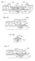
Referring to FIG. 1 of the drawings, thereference numeral 100 generally designates a top view of a MEMS switch embodying features of the present invention. TheMEMS switch 100 generally comprises aflexible membrane 110 suspended by supports orposts 112 over at least oneelectrode 114. Theflexible membrane 110 and theelectrode 114 are preferably constructed from a conductive material, such as aluminum, gold, copper, platinum, nickel, or the like, such that when a voltage, such as a direct-current (DC) voltage, an alternating-current (AC) voltage, a radio-frequency (RF) voltage, or the like, but preferably a DC voltage, is applied to either theflexible membrane 110 or theelectrode 114, theflexible membrane 110 is attracted to, i.e., pulled-down to, theelectrode 114. In this actuated state, signals are allowed to be transmitted between theflexible membrane 110 and theelectrode 114, such as from the RF In120 to the RF Out122.
As will be discussed in greater detail below with reference to FIGS. 2 and 3, one or more insulating structures orposts 116 are positioned to prevent theflexible membrane 110 from contacting theelectrode 114. Preferably, theinsulating structures 116 are constructed from an insulating material such as silicon nitride, silicon dioxide, a dielectric material, or the like.
It should be noted that the MEMS switch depicted throughout the present disclosure comprises a typical MEMS switch for illustrative purposes only, and is not to limit the present invention in any manner. Other shapes and configurations, such as circles, ovals, rectangles, and the like, of theflexible membrane 110 and theelectrode 114 may be used within the spirit of the present invention. Additionally, the spacing, shape, number, and configuration of theinsulating structures 116 are depicted for illustrative purposes only as a 3×4 array. The spacing, shape, number, and configuration of theinsulating structures 116 are dependent, among other things, the flexibility of the chosen flexible membrane and the DC voltages used. Other spacing, shapes, numbers, and configurations ofinsulating structures 116 may be used without departing from the spirit of the present invention. Moreover, only a portion of the insulating posts may be used to prevent theflexible membrane 110 from contacting theelectrode 114. For example, theinsulating structures 116 may be positioned along a side of theelectrode 114 protruding toward the center of theelectrode 114, such that theflexible membrane 110 only contacts a portion of theinsulating structures 116.
Moreover, a variety of configurations or constructions ofsupports 112 for themembrane 110 and acantilever 810 can be employed, such as the upwardly extending sides of a well formed by an extension of asubstrate 212 and adielectric buffer layer 216, as shown in FIGS. 2,3,4,5,11,12A, and12B. In another configuration,metal posts 816 are formed on thedielectric buffer layer 216, integrally with a portion of themembrane 110 and the flexible portion of acantilever 810, as shown in FIGS. 7,8A,8B, and9. Other means of providing supports for theflexible membrane 110 will also be apparent and are contemplated by the invention.
Additionally, the inclusion of theinsulating structures 116 is the preferred embodiment and allows for a moreflexible membrane 110 that is less susceptible to failure due to repetitive flexes. Alternatively, the voltage,flexible membrane 110, and the spacing between theflexible membrane 110 and theelectrode 114 may be adjusted such that theflexible membrane 110 is not capable of stretching or flexing to contact theelectrode 114. This alternative embodiment, however, is not preferred because it is less mechanically robust and is more susceptible to failure.
Furthermore, the present disclosure discusses the invention in terms of a single MEMS switch. The present invention, however, may be used in a series or shunt configuration, or in combinations of series and shunt switches to configure a multi-throw switch. The use of the present invention in other configurations is considered known to a person of ordinary skill in the art upon a reading of the present disclosure.
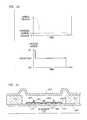
FIG. 2 is a side view of the MEMS illustrated in FIG. 1 to more clearly identify the components and their structural relationship. In one embodiment, thesupports 112 are part of a substrate212 (not shown in FIG. 1 for clarity) in which a cavity has been etched creating agaseous gap 214 of approximately 3-6 microns intermediate theflexible membrane 110 and theelectrode 114. Thesubstrate 212 is preferably constructed of insulating materials such as ceramics (alumina, beryllium oxide), glass, or semiconductors (high-resistivity silicon, gallium arsenide, indium phosphide), or the like. Optionally, adielectric buffer layer 216 is preferably placed on top of thesubstrate 212 to further insulate theflexible membrane 110, theelectrode 114, the input/output connections, and other electrical components mounted to the substrate.
Theelectrode 114 is deposited in the bottom of thecavity 214 on top of thedielectric buffer layer 216, and is typically 0.5-3 microns thick. Thedielectric structures 116, which are preferably 0.05-0.25 microns thick, are then deposited on theelectrode 114. Preferably, thegaseous gap 214 comprises a gaseous substance, such as air, nitrogen, noble gases, and the like, that is inert and an effective insulator betweenelectrode 114 and theflexible membrane 110.
Alternatively, supports112 may be constructed upon a substrate from which theflexible membrane 110 may be suspended. In this alternative embodiment, the material, preferably a metal, is deposited upon the substrate 2-6 microns thick, or of a thickness greater than the electrode and the desired gaseous gap. The construction of this alternative embodiment will be apparent to one skilled in the art in light of this disclosure.
Furthermore, theflexible membrane 110 preferably comprisesstress absorbers 210 to reduce the stress on theflexible membrane 110 when theflexible membrane 110 is pulled down, as discussed below with reference to FIG.3. The stress absorbers are described in detail in U.S. Pat. No. 6,100,477 to Randall et al., entitled “Recessed Etch RF Micro-Electro-Mechanical Switch” and is incorporated by reference herein for all purposes.
Furthermore, the manufacturing techniques referred to herein, such as etching, additive and subtractive processes, and the like, are considered known to a person of ordinary skill in the art, and, therefore, will not be discussed in greater detail except insofar as is necessary to adequately describe the present invention.
FIG. 3 is a side view of theMEMS switch 100 in an actuated state, i.e., with a DC voltage applied to theelectrode 114, causing theflexible membrane 110 to be attracted to theelectrode 114. When a sufficient DC voltage is applied to theelectrode 114, thegaseous gap 214 becomes charged and theflexible membrane 110 is pulled-down towards theelectrode 114, possibly contacting at least a portion of one or moreinsulating structures 116. As discussed above, the insulatingstructures 116 prevent theflexible membrane 110 from contacting theelectrode 114, creating agaseous gap 214 that acts as a capacitance, which, when actuated, allows high-frequency signals to be transmitted between the RF In120 and the RF Out122 (as illustrated in FIG.1). Upon removing the DC voltage from theelectrode 114, the restoring forces of theflexible membrane 110 causes theflexible membrane 110 to return to the initial position illustrated in FIG.2.
As will be appreciated by one skilled in the art, the use of a gaseous material for thegaseous gap 214 reduces the dielectric charging and trapping known to occur in many solid dielectric materials, reduces stiction by reducing the contact area, and reduces the need for smooth substrate, dielectric, and electrode surfaces. Thinner flexible membranes were generally preferred in the prior art, because, among other things, thinner flexible membranes make more complete contact with the underlying surface, thus providing a greater area of contact. In addition, thinner flexible membranes typically are smoother than thicker flexible membranes; thus reducing the wear and tear of the flexible membrane as it contacts the dielectric material, as well as enhancing the contact area through the reduction of the number of asperities or unevenness that would reduce the total contact area. Thinner flexible membranes, however, create a higher resistance in the RF path, decreasing the performance of the MEMS. Since, as noted above, theflexible membrane 110 contacts only the insulatingstructures 116, theflexible membrane 110 does not need to be as smooth and, therefore, may be thicker, which reduces the resistance in the RF path, increasing the switch performance.
Furthermore, the amount of voltage required to operate the switch is dependent upon, among other things, the properties of theflexible membrane 110. It is preferred that the flexible membrane react quickly, preferably within microseconds or tens of microseconds, to the application and/or removal of the DC voltage. Higher DC voltages will cause theflexible membrane 110 to react quicker, but is generally not available in many handheld or portable devices. Lower DC voltages, however, are not actuated as quickly and require a thinnerflexible membrane 110. The precise configuration is dependent upon the intended use and can be determined by a person of ordinary skill in the art upon a reading of the present disclosure.
FIG. 4 is an alternative embodiment of the present invention that further isolates the dielectric structures from the electrode. Generally, the embodiment illustrated in FIG. 4 further reduces the probability of the insulating structures116 (shown in FIG. 2) trapping charges and affecting the performance of theMEMS switch 100 by electrically separating the insulatingstructures 116 from the electrode114 (shown in FIGS.2 and3). Accordingly,reference numeral 400 generally designates a side view of a MEMS in which insulatingstructures 410 are deposited uponconductive structures 412, which are electrically separated from theelectrode 114. TheMEMS switch 400 is preferably manufactured similarly to theMEMS switch 100, except that the metal, i.e., the conductive material of theelectrode 114, around each of the insulatingstructures 410 is removed such that theconductive structures 412 are not electrically coupled to theelectrode 114.
FIG. 5 is yet another alternative embodiment that may further reduces the probability of the insulating structures trapping charges, affecting the performance of the MEMS switch. Accordingly,reference numeral 500 of FIG. 5 generally designates a side view of a MEMS switch in which insulatingstructures 510 are electrically isolated from theelectrode 114. The insulatingstructures 510 are not coupled to the electrode or other conductive material, thereby further reducing the ability of the structures to trap and transmit a charge.
Preferably, theMEMS switch 500 is manufactured as described above with reference to FIG. 4, except that the area taken by the conductive structures412 (FIG. 4) is also removed. Briefly, a conductive material is deposited upon the dielectric buffer layer, which was deposited upon the substrate as discussed above. The conductive material is etched to form the desired pattern of theelectrode 114, specifically removing the conductive material from the locations that the insulatingstructures 510 are to reside. An insulating material is deposited upon the surface and etched to form the insulatingstructures 510. Therefore, the insulatingstructures 510 are deposited upon thedielectric buffer layer 216 and extends above theelectrode 114, preferably by 0.05-0.25 microns.
FIGS. 6 and 7 are a top view and a side view, respectively, that illustrate an alternative embodiment of the present invention in which fewer insulating structures are used and are spaced further apart. Preferably, insulatingstructures 612 are positioned on either side of theelectrode 114 in order to maximize the area of the exposed electrode. Accordingly, insulatingstructures 612 are positioned such that a stiffeningmember 610, which is coupled to and/or integrated in theflexible membrane 110, overlaps the insulatingstructures 612. The stiffeningmember 610 may be a separate component, such as dielectric layer, a metallic layer, or a combination thereof, coupled to theflexible membrane 110, or incorporated into the design and manufacturing of the flexible membrane, such that the flexible membrane comprises a thicker, less flexible portion or incorporates a stiffening component, such as ridges, corrugation, or the like.
Optionally, additional insulating structures, such as insulatingstructure 614, may be added as desired to insure that the flexible membrane does not come into contact with theelectrode 114. The positions and shapes of the insulatingstructures
FIGS. 8A and 9 illustrate the “OFF” state and the “ON” state, respectively, of yet another embodiment of the present invention in which the flexible membrane is replaced with a cantilever. Acantilever 810 is suspended above theelectrode 114 and one or moreinsulating structures 812. Applying a voltage to theelectrode 114 causes thecantilever 810 to be pulled down towards theelectrode 114. Thecantilever 810 is prevented from contacting theelectrode 114 by the insulatingstructures 812, causing thegaseous gap 214 to act as a capacitor. An optionalinsulating structure 814 may be positioned on the opposing side of theelectrode 114 from the insulatingstructure 812 to ensure that thecantilever 810 does not contact theelectrode 114. The optionalinsulating structure 814 also reduces the tension of the cantilever by not allowing it to flex further than is required to charge thegaseous gap 214.
It should be noted, however, that voltage breakdown may occur in the foregoing embodiments if the applied voltage exceeds the capability of the gas to stand it off. Voltage breakdown, generally referred to as a Townsend breakdown, occurs when emitted electrons strike molecules in the gas, which emit more electrons, and the process cascades until charges arc across the gap. In these situations, it may be desirable to utilize a metal with a high work function to increase the voltage breakdown of the switch. The use of a high-work-function metal, such as platinum, nickel, gold, and the like, reduces the affinity of electrons to be emitted that could eventually cause voltage breakdown.
Similarly, the gaps between the flexible membrane and the electrode, such as thegaseous gap 214, may be filled with gases that have high electronegativity to further reduce the possibility of the switch failing. Gases, such as sulpher hexafloride, carbon dioxide, and the like, exhibit high eltronegativity that reduces the affinity for a cascading breakdown after emitted electrons have struck the gas molecules.
Additionally, the DC control voltage may be varied such that the number of volts is reduced once the flexible membrane contacts one or more of the insulating structures. Generally, the amount of voltage required to pull down the flexible membrane to the insulating structures is greater than the amount of voltage required to maintain the flexible membrane in the pulled-down state, i.e., the “ON” position. Switch actuation voltages are typically 30-60 volts when the membrane is suspended in the initial “OFF” position. After theflexible membrane 110 has been pulled down, however, the electrical field is much stronger, and, therefore, the holding force is much stronger. Therefore, the applied voltage can be reduced to just above the required holding voltage, which ranges from 5-15 volts.
FIG. 8B illustrates an optional configuration in which at least one of thestructures flexible membrane 110, or thecantilever 810, onto the insulatingstructures structure 812 is shown. Such a circuit would employ ametallic layer 816 deposited or otherwise positioned between at least the insulatingstructure 812 and the underlyingdielectric buffer layer 216, to sense an electrical charge variation in thestructure 812, upon contact with thecantilever 810. Once theflexible membrane 110 orcantilever 810 has been sensed in the “ON” position, the voltage can be immediately reduced from 30-60 volts to slightly above 5-15 volts. It should be noted that the voltages may vary dependent upon, among other things, the type of materials and gases, and the geometries that are used.
FIG. 10 illustrates yet another optional control voltage management scheme that may be utilized in conjunction with MEMS switch, such as those discussed in the present disclosure, as well as with other capacitive switches, such as the capacitive switch disclosed in U.S. Pat. No. 6,100,477, which is incorporated herein by reference for all purposes. Shown in the upper graph by a broken line is the switch voltage resulting over time as the switch actuates from the OFF to the ON positions and then is returned the OFF position. Shown in the lower graph by a solid line is the voltage source concomitantly applied to the switch over the same time period shown in the upper graph, during the OFF-ON-OFF actuation and return steps.
Referring to both graphs in FIG. 10, actuation of the switch is initiated by connecting a voltage source to the switch electrodes, illustrated by the solid line. Preferably, an actuation voltage is applied for a period of time, typically 0.10-1.0 microseconds, sufficient to charge the switch capacitance to its maximum value Q. This causes actuation of the switch, which in turn results in a drop in the switch voltage (broken line) to a lower level throughout the duration of the switch hold-down. This effect results from an increase in capacitance while maintaining a substantially fixed amount of charge on the switch plates. Upon charging the capacitance, the voltage source is disconnected, effectively leaving charge Q on the plates of the switch. Charge Q provides sufficient attraction between theflexible membrane 110 and theelectrode 114 so as to cause theflexible membrane 110 to actuate onto the insulatingstructures 116, allowing RF energy to pass between theflexible membrane 110 and theelectrode 114, in the switch ON state. As the electrode actuates and the capacitance between theflexible membrane 110 and theelectrode 114 increases, the voltage level between theelectrode 114 andflexible membrane 110 decreases proportionately. With the voltage source disconnected, there is no means available for the net charge to change and the product of capacitance and voltage remains constant. As a result, the voltage on the dielectric is minimized to the amount of voltage that is necessary to accomplish switching. Moreover, this control voltage management technique reduces or substantially eliminates the risk of electrical arching between theflexible membrane 110 and the electrode as they approach the ON state. The Switch is returned to the OFF position by reconnecting the DC voltage supply that has been switched to the OFF position or by discharging the applied charge Q.
FIG. 11 illustrates yet another embodiment of the present invention that may reduce the likelihood of a voltage breakdown by depositing a thin dielectric or insulating layer onto the electrode. FIG. 11 represents the embodiment illustrated in FIG. 4 for illustrative purposes only, and, accordingly, the application of a thin dielectric layer onto the electrode may be used in conjunction with other embodiments, some of which are discussed within the present disclosure, such as the embodiments illustrated in FIGS. 1-9 and11-12. The application of the thin dielectric layer with other embodiments is considered known to a person of ordinary skill in the art upon a reading of the present disclosure.
Athin dielectric layer 1110, preferably approximately 100 angstroms thick, may be applied over the full surface of the electrode, preferably after etching the electrode and prior to depositing the insulatingstructures 410, to further reduce the possibility of the MEMS switch failing. This layer, comprising a dielectric material, such as silicon nitride, silicon oxide, Teflon® or the like, hinders the ability of charges to traverse the gap, thereby reducing the likelihood of a voltage breakdown.
FIG. 12A illustrates yet another embodiment of the present invention that utilizes dielectric structures coupled to theflexible membrane 110. FIG. 12A represents the embodiment illustrated in FIGS. 1-3 for illustrative purposes only, and, accordingly, coupling one or more dielectric structures to theflexible membrane 110 may be used in conjunction with other embodiments, some of which are discussed within the present disclosure, such as the embodiments illustrated in FIGS. 1-9 and11.
Insulatingstructures 1210 are coupled to theflexible membrane 110. In a similar manner as the other embodiments discussed within the present disclosure, the insulatingstructures 1210 prevent theflexible membrane 110 from contacting theelectrode 114, and create a gaseous gap that allows the transmission of high-frequency signals when charged.
FIG. 12B illustrates yet another embodiment of the present invention that utilizes dielectric structures coupled to thecantilever 810. FIG. 12B represents the embodiment illustrated in FIGS. 8A-9 for illustrative purposes only, and, accordingly, coupling one or more dielectric structures to thecantilever 810 may be used in conjunction with other embodiments, some of which are discussed within the present disclosure.
Insulatingstructures 1220 are coupled to thecantilever 810. In a similar manner as the other embodiments discussed within the present disclosure, the insulatingstructures 1220 prevent thecantilever 810 from contacting theelectrode 114, and create a gaseous gap that allows the transmission of high-frequency signals when charged.
It is understood that the present invention can take many forms and embodiments. Accordingly, several variations may be made in the foregoing without departing from the spirit or the scope of the invention. For example, fixed conductors may be positioned on either side of a movable electrode, such that the switch electrically actuates in both directions and naturally release due to restoring forces in the other direction.
Having thus described the present invention by reference to certain of its preferred embodiments, it is noted that the embodiments disclosed are illustrative rather than limiting in nature and that a wide range of variations, modifications, changes, and substitutions are contemplated in the foregoing disclosure and, in some instances, some features of the present invention may be employed without a corresponding use of the other features. Many such variations and modifications may be considered obvious and desirable by those skilled in the art based upon a review of the foregoing description of preferred embodiments. Accordingly, it is appropriate that the appended claims be construed broadly and in a manner consistent with the scope of the invention.
Claims (44)
1. An apparatus comprising:
a first electrode;
a second electrode configured to be displaced toward the first electrode in response to the application of a voltage differential with respect to the first electrode;
one or more insulating structures, wherein at least a portion of the insulating structures prevent the second electrode from contacting the first electrode; and
a gaseous capacitive gap is formed and maintained between the first and second electrodes when the voltage differential is applied.
2. The apparatus ofclaim 1 , further comprising means for discontinuing the application of the voltage differential after charging the gaseous capacitive gap.
3. The apparatus ofclaim 1 , further comprising:
means for discontinuing the application of the voltage differential after charging the gaseous capacitive gap; and
means for discharging the gaseous capacitive gap.
4. The apparatus ofclaim 1 , wherein the second electrode comprises a flexible membrane suspended over the first electrode.
5. The apparatus ofclaim 1 , wherein the second electrode comprises a cantilever.
6. An apparatus comprising:
one or more electrodes;
one or more insulating structures;
an electrically conductive member suspended above the electrodes, wherein at least a portion of the insulating structures prevent the electrically conductive member from contacting the electrodes, wherein the electrically conductive member is attracted to the electrodes when a voltage is applied to the electrode, and wherein a gaseous capacitive gap between the electrically conductive member and the electrodes is maintained when voltage is applied to the electrode.
7. The apparatus ofclaim 6 , further comprising means for disconnecting the voltage after charging the gaseous capacitive gap.
8. The apparatus ofclaim 6 , further comprising:
means for disconnecting the voltage after charging the gaseous capacitive gap; and
means for discharging the gaseous capacitive gap.
9. The apparatus ofclaim 6 , wherein the insulating structures comprise a dielectric material deposited on the electrodes.
10. The apparatus ofclaim 6 , wherein the insulating structures are not electrically coupled to the electrodes.
11. The apparatus ofclaim 6 , wherein the insulating structures comprise a dielectric material deposited on an electrically conductive material that is not electrically coupled to the electrodes.
12. The apparatus ofclaim 6 , wherein the insulating structures are coupled to the electrically conductive member.
13. The apparatus ofclaim 12 , wherein the electrically conductive member comprises a flexible membrane.
14. The apparatus ofclaim 12 , wherein the electrically conductive member comprises a cantilever.
15. The apparatus ofclaim 13 or14 , wherein the insulating structures comprise a dielectric material coupled to the electrically conductive member.
16. The apparatus ofclaim 6 , further comprising a dielectric layer deposited on the electrode.
17. The apparatus ofclaim 6 , wherein the electrically conductive member comprises at least one of aluminum, gold, copper, platinum, and nickel.
18. The apparatus ofclaim 6 , wherein the electrode comprises at least one of aluminum, gold, copper, platinum, and nickel.
19. The apparatus ofclaim 6 , wherein the insulating structures comprise at least one of silicon nitride and silicon dioxide.
20. The apparatus ofclaim 6 , wherein the gaseous capacitive gap comprises at least one of air, nitrogen, inert gasses, and noble gases.
21. An apparatus comprising:
a substrate with a cavity formed therein;
one or more electrodes placed within the cavity;
one or more insulating structures having a portion positioned above the-surface of the electrodes; and
a conductive member having a flexible portion wherein the conductive member is suspended by the flexible portion above the electrodes, wherein a gaseous space is maintained intermediate the conductive member and the electrodes.
22. The apparatus ofclaim 21 , wherein the insulating structures comprises a dielectric material deposited on the electrodes.
23. The apparatus ofclaim 21 , wherein the insulating structures are not electrically coupled to the electrodes.
24. The apparatus ofclaim 21 , wherein the insulating structures comprise a dielectric material deposited on a conductive material that is not electrically coupled to the electrodes.
25. The apparatus ofclaim 21 , wherein the insulating structures are couple ed to the conductive member.
26. The apparatus ofclaim 21 , further comprising a dielectric layer deposited on the electrodes.
27. The apparatus ofclaim 21 , wherein the conductive member is either a flexible membrane or a cantilever.
28. A method of providing micro-electro-mechanical switching of high-frequency signals, the method comprising the steps of:
suspending a conductive, flexible membrane over an electrode, creating a switch;
actuating the switch by applying voltage to the electrode, wherein the voltage causes the flexible membrane to be attracted to the electrode, wherein the flexible membrane is prevented from contacting the electrode by at least a portion of one or more insulating structures, and wherein a gaseous capacitive gap is maintained between the flexible membrane and the electrode thereby allowing high-frequency signals to be transmitted to the electrode.
29. The method ofclaim 28 , further comprising disconnecting the voltage when the gaseous capacitive gap is charged.
30. The method ofclaim 28 , wherein the insulating structures comprise a dielectric material deposited on the electrodes.
31. The method ofclaim 28 , wherein the insulating structures are not electrically coupled to the electrode.
32. The method ofclaim 28 , wherein the insulating structures comprise a dielectric material deposited on a conductive material that is not electrically coupled to the electrodes.
33. The method ofclaim 28 , wherein the insulating structures are coupled to the flexible membrane.
34. The method ofclaim 28 , the electrodes comprise a conductive material covered by a dielectric layer.
35. A method of providing micro-electro-mechanical switching of high-frequency signals, the method comprising the steps of:
suspending a conductive cantilever having a flexible portion over an electrode, creating a switch;
actuating the switch by applying voltage to the electrode, wherein the voltage causes the flexible portion of the cantilever to flex the cantilever toward the electrode, wherein the cantilever is prevented from contacting the electrode by at least a portion of one or more insulating structures, and wherein a gaseous capacitive gap is maintained between the cantilever and the electrode thereby allowing high-frequency signals to be transmitted to the electrode.
36. The method ofclaim 35 , further comprising disconnecting the voltage when the gaseous capacitive gap is charged.
37. The method ofclaim 35 , wherein the insulating structures comprise a dielectric material deposited on the electrodes.
38. The method ofclaim 35 , wherein the insulating structures are not electrically coupled to the electrode.
39. The method ofclaim 35 , wherein the insulating structures comprise a dielectric material deposited on a conductive material that is not electrically coupled to the electrodes.
40. The method ofclaim 35 , wherein the insulating structures are coupled to the cantilever.
41. The method ofclaim 35 , the electrodes comprise a conductive material covered by a dielectric layer.
42. An apparatus, comprising:
a first electrically conductive member;
a second electrically conductive member; and
a gaseous gap providing a capacitance formed and maintained between the first and second electrically conductive members, the gap allowing high-frequency signals to be transmitted between the first and second members.
43. The apparatus ofclaim 42 , further comprising at least one insulating structure for separating the first and second electrically conductive members to maintain the gaseous capacitive gap.
44. The apparatus ofclaim 43 , wherein the insulating structure does not retain sufficient dielectric charging to substantially degrade the capacitance of the gaseous gap.
Priority Applications (1)
| Application Number | Priority Date | Filing Date | Title |
|---|---|---|---|
| US10/068,399US6608268B1 (en) | 2002-02-05 | 2002-02-05 | Proximity micro-electro-mechanical system |
Applications Claiming Priority (1)
| Application Number | Priority Date | Filing Date | Title |
|---|---|---|---|
| US10/068,399US6608268B1 (en) | 2002-02-05 | 2002-02-05 | Proximity micro-electro-mechanical system |
Publications (2)
| Publication Number | Publication Date |
|---|---|
| US20030146079A1 US20030146079A1 (en) | 2003-08-07 |
| US6608268B1true US6608268B1 (en) | 2003-08-19 |
Family
ID=27659031
Family Applications (1)
| Application Number | Title | Priority Date | Filing Date |
|---|---|---|---|
| US10/068,399Expired - LifetimeUS6608268B1 (en) | 2002-02-05 | 2002-02-05 | Proximity micro-electro-mechanical system |
Country Status (1)
| Country | Link |
|---|---|
| US (1) | US6608268B1 (en) |
Cited By (146)
| Publication number | Priority date | Publication date | Assignee | Title |
|---|---|---|---|---|
| US20030099385A1 (en)* | 2001-11-23 | 2003-05-29 | Xiaolan Zeng | Segmentation in medical images |
| US20040032185A1 (en)* | 2002-07-30 | 2004-02-19 | Yoshichika Kato | Micromachined moving device |
| WO2004026757A3 (en)* | 2002-09-20 | 2004-06-24 | Iridigm Display Corp | Controlling electromechanical behavior of structures within a microelectromechanical systems device |
| US20050011739A1 (en)* | 2001-10-01 | 2005-01-20 | Gill Michael John | Electrical apparatus |
| US7012726B1 (en) | 2003-11-03 | 2006-03-14 | Idc, Llc | MEMS devices with unreleased thin film components |
| US20060066935A1 (en)* | 2004-09-27 | 2006-03-30 | Cummings William J | Process for modifying offset voltage characteristics of an interferometric modulator |
| US20060066640A1 (en)* | 2004-09-27 | 2006-03-30 | Manish Kothari | Display region architectures |
| US20060164193A1 (en)* | 2002-11-28 | 2006-07-27 | Philippe Robert | Electrostatic micro-switch for components with low operating voltages |
| US20060229045A1 (en)* | 2005-04-08 | 2006-10-12 | Samsung Electronics Co., Ltd. | Tri-state RF switch |
| US20060238951A1 (en)* | 2002-12-31 | 2006-10-26 | The Regents Of The University Of California | MEMS Fabrication on a Laminated substrate |
| US7161730B2 (en) | 2004-09-27 | 2007-01-09 | Idc, Llc | System and method for providing thermal compensation for an interferometric modulator display |
| US7172915B2 (en) | 2003-01-29 | 2007-02-06 | Qualcomm Mems Technologies Co., Ltd. | Optical-interference type display panel and method for making the same |
| US20070040777A1 (en)* | 2004-09-27 | 2007-02-22 | Cummings William J | Methods and devices for inhibiting tilting of a mirror in an interferometric modulator |
| US7193768B2 (en) | 2003-08-26 | 2007-03-20 | Qualcomm Mems Technologies, Inc. | Interference display cell |
| US7198973B2 (en) | 2003-04-21 | 2007-04-03 | Qualcomm Mems Technologies, Inc. | Method for fabricating an interference display unit |
| US20070103843A1 (en)* | 2003-12-26 | 2007-05-10 | Commissariat A L'energie Atomique | Electrostatic mems components permitting a large vertical displacement |
| US7221495B2 (en) | 2003-06-24 | 2007-05-22 | Idc Llc | Thin film precursor stack for MEMS manufacturing |
| US7236284B2 (en) | 1995-05-01 | 2007-06-26 | Idc, Llc | Photonic MEMS and structures |
| US7250315B2 (en) | 2002-02-12 | 2007-07-31 | Idc, Llc | Method for fabricating a structure for a microelectromechanical system (MEMS) device |
| US7265477B2 (en)* | 2004-01-05 | 2007-09-04 | Chang-Feng Wan | Stepping actuator and method of manufacture therefore |
| US7289259B2 (en) | 2004-09-27 | 2007-10-30 | Idc, Llc | Conductive bus structure for interferometric modulator array |
| US7291921B2 (en) | 2003-09-30 | 2007-11-06 | Qualcomm Mems Technologies, Inc. | Structure of a micro electro mechanical system and the manufacturing method thereof |
| US7297471B1 (en) | 2003-04-15 | 2007-11-20 | Idc, Llc | Method for manufacturing an array of interferometric modulators |
| US7302157B2 (en) | 2004-09-27 | 2007-11-27 | Idc, Llc | System and method for multi-level brightness in interferometric modulation |
| US7304784B2 (en) | 2004-09-27 | 2007-12-04 | Idc, Llc | Reflective display device having viewable display on both sides |
| US20070279457A1 (en)* | 2006-06-06 | 2007-12-06 | Xerox Corporation | Electrostatic actuator and method of making the electrostatic actuator |
| US20080013144A1 (en)* | 2004-09-27 | 2008-01-17 | Idc, Llc | Microelectromechanical device with optical function separated from mechanical and electrical function |
| US7321457B2 (en) | 2006-06-01 | 2008-01-22 | Qualcomm Incorporated | Process and structure for fabrication of MEMS device having isolated edge posts |
| US7321456B2 (en) | 2004-09-27 | 2008-01-22 | Idc, Llc | Method and device for corner interferometric modulation |
| US20080016964A1 (en)* | 2006-07-19 | 2008-01-24 | Koury Daniel N | MEMS device and method of reducing stiction in a MEMS device |
| US7349136B2 (en) | 2004-09-27 | 2008-03-25 | Idc, Llc | Method and device for a display having transparent components integrated therein |
| US7369296B2 (en) | 2004-09-27 | 2008-05-06 | Idc, Llc | Device and method for modifying actuation voltage thresholds of a deformable membrane in an interferometric modulator |
| US7369292B2 (en) | 2006-05-03 | 2008-05-06 | Qualcomm Mems Technologies, Inc. | Electrode and interconnect materials for MEMS devices |
| US7372613B2 (en) | 2004-09-27 | 2008-05-13 | Idc, Llc | Method and device for multistate interferometric light modulation |
| US7373026B2 (en) | 2004-09-27 | 2008-05-13 | Idc, Llc | MEMS device fabricated on a pre-patterned substrate |
| US7372619B2 (en) | 1994-05-05 | 2008-05-13 | Idc, Llc | Display device having a movable structure for modulating light and method thereof |
| US20080121503A1 (en)* | 2006-11-02 | 2008-05-29 | Sampsell Jeffrey B | Compatible MEMS switch architecture |
| US7382515B2 (en) | 2006-01-18 | 2008-06-03 | Qualcomm Mems Technologies, Inc. | Silicon-rich silicon nitrides as etch stops in MEMS manufacture |
| US7385744B2 (en) | 2006-06-28 | 2008-06-10 | Qualcomm Mems Technologies, Inc. | Support structure for free-standing MEMS device and methods for forming the same |
| US7405863B2 (en) | 2006-06-01 | 2008-07-29 | Qualcomm Mems Technologies, Inc. | Patterning of mechanical layer in MEMS to reduce stresses at supports |
| US7405861B2 (en) | 2004-09-27 | 2008-07-29 | Idc, Llc | Method and device for protecting interferometric modulators from electrostatic discharge |
| US7417784B2 (en) | 2006-04-19 | 2008-08-26 | Qualcomm Mems Technologies, Inc. | Microelectromechanical device and method utilizing a porous surface |
| US7417783B2 (en) | 2004-09-27 | 2008-08-26 | Idc, Llc | Mirror and mirror layer for optical modulator and method |
| US7420728B2 (en) | 2004-09-27 | 2008-09-02 | Idc, Llc | Methods of fabricating interferometric modulators by selectively removing a material |
| US7420725B2 (en) | 2004-09-27 | 2008-09-02 | Idc, Llc | Device having a conductive light absorbing mask and method for fabricating same |
| US7450295B2 (en) | 2006-03-02 | 2008-11-11 | Qualcomm Mems Technologies, Inc. | Methods for producing MEMS with protective coatings using multi-component sacrificial layers |
| US20080283374A1 (en)* | 2007-05-17 | 2008-11-20 | Matsushita Electric Industrial Co., Ltd. | Electromechanical element, driving method of the electromechanical element and electronic equipment provided with the same |
| US20080311690A1 (en)* | 2007-04-04 | 2008-12-18 | Qualcomm Mems Technologies, Inc. | Eliminate release etch attack by interface modification in sacrificial layers |
| US7471442B2 (en) | 2006-06-15 | 2008-12-30 | Qualcomm Mems Technologies, Inc. | Method and apparatus for low range bit depth enhancements for MEMS display architectures |
| US20090002804A1 (en)* | 2007-06-29 | 2009-01-01 | Qualcomm Mems Technologies, Inc. | Electromechanical device treatment with water vapor |
| US20090009845A1 (en)* | 2007-07-02 | 2009-01-08 | Qualcomm Incorporated | Microelectromechanical device with optical function separated from mechanical and electrical function |
| US7476327B2 (en) | 2004-05-04 | 2009-01-13 | Idc, Llc | Method of manufacture for microelectromechanical devices |
| US7492502B2 (en) | 2004-09-27 | 2009-02-17 | Idc, Llc | Method of fabricating a free-standing microstructure |
| US7527998B2 (en) | 2006-06-30 | 2009-05-05 | Qualcomm Mems Technologies, Inc. | Method of manufacturing MEMS devices providing air gap control |
| US7527995B2 (en) | 2004-09-27 | 2009-05-05 | Qualcomm Mems Technologies, Inc. | Method of making prestructure for MEMS systems |
| US7527996B2 (en) | 2006-04-19 | 2009-05-05 | Qualcomm Mems Technologies, Inc. | Non-planar surface structures and process for microelectromechanical systems |
| US7532377B2 (en) | 1998-04-08 | 2009-05-12 | Idc, Llc | Movable micro-electromechanical device |
| US7534640B2 (en) | 2005-07-22 | 2009-05-19 | Qualcomm Mems Technologies, Inc. | Support structure for MEMS device and methods therefor |
| US7535621B2 (en) | 2006-12-27 | 2009-05-19 | Qualcomm Mems Technologies, Inc. | Aluminum fluoride films for microelectromechanical system applications |
| US7547565B2 (en) | 2005-02-04 | 2009-06-16 | Qualcomm Mems Technologies, Inc. | Method of manufacturing optical interference color display |
| US7547568B2 (en) | 2006-02-22 | 2009-06-16 | Qualcomm Mems Technologies, Inc. | Electrical conditioning of MEMS device and insulating layer thereof |
| US7550810B2 (en) | 2006-02-23 | 2009-06-23 | Qualcomm Mems Technologies, Inc. | MEMS device having a layer movable at asymmetric rates |
| US20090159410A1 (en)* | 2007-12-20 | 2009-06-25 | General Electric Company | Mems microswitch having a conductive mechanical stop |
| US7553684B2 (en) | 2004-09-27 | 2009-06-30 | Idc, Llc | Method of fabricating interferometric devices using lift-off processing techniques |
| US7554711B2 (en) | 1998-04-08 | 2009-06-30 | Idc, Llc. | MEMS devices with stiction bumps |
| US7554714B2 (en) | 2004-09-27 | 2009-06-30 | Idc, Llc | Device and method for manipulation of thermal response in a modulator |
| US7564612B2 (en) | 2004-09-27 | 2009-07-21 | Idc, Llc | Photonic MEMS and structures |
| US7566664B2 (en) | 2006-08-02 | 2009-07-28 | Qualcomm Mems Technologies, Inc. | Selective etching of MEMS using gaseous halides and reactive co-etchants |
| US7567373B2 (en) | 2004-07-29 | 2009-07-28 | Idc, Llc | System and method for micro-electromechanical operation of an interferometric modulator |
| US7570415B2 (en) | 2007-08-07 | 2009-08-04 | Qualcomm Mems Technologies, Inc. | MEMS device and interconnects for same |
| US7580172B2 (en) | 2005-09-30 | 2009-08-25 | Qualcomm Mems Technologies, Inc. | MEMS device and interconnects for same |
| US20090260960A1 (en)* | 2008-04-21 | 2009-10-22 | Formfactor, Inc. | Switch for use in microelectromechanical systems (mems) and mems devices incorporating same |
| US7612933B2 (en) | 2008-03-27 | 2009-11-03 | Qualcomm Mems Technologies, Inc. | Microelectromechanical device with spacing layer |
| US7623287B2 (en) | 2006-04-19 | 2009-11-24 | Qualcomm Mems Technologies, Inc. | Non-planar surface structures and process for microelectromechanical systems |
| US7630119B2 (en) | 2004-09-27 | 2009-12-08 | Qualcomm Mems Technologies, Inc. | Apparatus and method for reducing slippage between structures in an interferometric modulator |
| US7629197B2 (en) | 2006-10-18 | 2009-12-08 | Qualcomm Mems Technologies, Inc. | Spatial light modulator |
| US7630114B2 (en) | 2005-10-28 | 2009-12-08 | Idc, Llc | Diffusion barrier layer for MEMS devices |
| US20090305010A1 (en)* | 2008-06-05 | 2009-12-10 | Qualcomm Mems Technologies, Inc. | Low temperature amorphous silicon sacrificial layer for controlled adhesion in mems devices |
| US7643202B2 (en) | 2007-05-09 | 2010-01-05 | Qualcomm Mems Technologies, Inc. | Microelectromechanical system having a dielectric movable membrane and a mirror |
| US7643199B2 (en) | 2007-06-19 | 2010-01-05 | Qualcomm Mems Technologies, Inc. | High aperture-ratio top-reflective AM-iMod displays |
| US7643203B2 (en) | 2006-04-10 | 2010-01-05 | Qualcomm Mems Technologies, Inc. | Interferometric optical display system with broadband characteristics |
| US7649671B2 (en) | 2006-06-01 | 2010-01-19 | Qualcomm Mems Technologies, Inc. | Analog interferometric modulator device with electrostatic actuation and release |
| US7652814B2 (en) | 2006-01-27 | 2010-01-26 | Qualcomm Mems Technologies, Inc. | MEMS device with integrated optical element |
| US7660058B2 (en) | 2005-08-19 | 2010-02-09 | Qualcomm Mems Technologies, Inc. | Methods for etching layers within a MEMS device to achieve a tapered edge |
| US7684104B2 (en) | 2004-09-27 | 2010-03-23 | Idc, Llc | MEMS using filler material and method |
| US20100077609A1 (en)* | 2008-09-29 | 2010-04-01 | Xerox Corporation | Buried traces for sealed electrostatic membrane actuators or sensors |
| US7706044B2 (en) | 2003-05-26 | 2010-04-27 | Qualcomm Mems Technologies, Inc. | Optical interference display cell and method of making the same |
| US7711239B2 (en) | 2006-04-19 | 2010-05-04 | Qualcomm Mems Technologies, Inc. | Microelectromechanical device and method utilizing nanoparticles |
| US7715079B2 (en) | 2007-12-07 | 2010-05-11 | Qualcomm Mems Technologies, Inc. | MEMS devices requiring no mechanical support |
| US7715085B2 (en) | 2007-05-09 | 2010-05-11 | Qualcomm Mems Technologies, Inc. | Electromechanical system having a dielectric movable membrane and a mirror |
| US7719500B2 (en) | 2004-09-27 | 2010-05-18 | Qualcomm Mems Technologies, Inc. | Reflective display pixels arranged in non-rectangular arrays |
| US7719752B2 (en) | 2007-05-11 | 2010-05-18 | Qualcomm Mems Technologies, Inc. | MEMS structures, methods of fabricating MEMS components on separate substrates and assembly of same |
| US7733552B2 (en) | 2007-03-21 | 2010-06-08 | Qualcomm Mems Technologies, Inc | MEMS cavity-coating layers and methods |
| US7742220B2 (en) | 2007-03-28 | 2010-06-22 | Qualcomm Mems Technologies, Inc. | Microelectromechanical device and method utilizing conducting layers separated by stops |
| US7746539B2 (en) | 2008-06-25 | 2010-06-29 | Qualcomm Mems Technologies, Inc. | Method for packing a display device and the device obtained thereof |
| US7763546B2 (en) | 2006-08-02 | 2010-07-27 | Qualcomm Mems Technologies, Inc. | Methods for reducing surface charges during the manufacture of microelectromechanical systems devices |
| US7768690B2 (en) | 2008-06-25 | 2010-08-03 | Qualcomm Mems Technologies, Inc. | Backlight displays |
| US7773286B2 (en) | 2007-09-14 | 2010-08-10 | Qualcomm Mems Technologies, Inc. | Periodic dimple array |
| US7782517B2 (en) | 2007-06-21 | 2010-08-24 | Qualcomm Mems Technologies, Inc. | Infrared and dual mode displays |
| US7781850B2 (en) | 2002-09-20 | 2010-08-24 | Qualcomm Mems Technologies, Inc. | Controlling electromechanical behavior of structures within a microelectromechanical systems device |
| US7795061B2 (en) | 2005-12-29 | 2010-09-14 | Qualcomm Mems Technologies, Inc. | Method of creating MEMS device cavities by a non-etching process |
| US7835061B2 (en) | 2006-06-28 | 2010-11-16 | Qualcomm Mems Technologies, Inc. | Support structures for free-standing electromechanical devices |
| US7847999B2 (en) | 2007-09-14 | 2010-12-07 | Qualcomm Mems Technologies, Inc. | Interferometric modulator display devices |
| US7855826B2 (en) | 2008-08-12 | 2010-12-21 | Qualcomm Mems Technologies, Inc. | Method and apparatus to reduce or eliminate stiction and image retention in interferometric modulator devices |
| US7859740B2 (en) | 2008-07-11 | 2010-12-28 | Qualcomm Mems Technologies, Inc. | Stiction mitigation with integrated mech micro-cantilevers through vertical stress gradient control |
| USRE42119E1 (en) | 2002-02-27 | 2011-02-08 | Qualcomm Mems Technologies, Inc. | Microelectrochemical systems device and method for fabricating same |
| US7884989B2 (en) | 2005-05-27 | 2011-02-08 | Qualcomm Mems Technologies, Inc. | White interferometric modulators and methods for forming the same |
| US7898723B2 (en) | 2008-04-02 | 2011-03-01 | Qualcomm Mems Technologies, Inc. | Microelectromechanical systems display element with photovoltaic structure |
| US7916980B2 (en) | 2006-01-13 | 2011-03-29 | Qualcomm Mems Technologies, Inc. | Interconnect structure for MEMS device |
| US7936497B2 (en) | 2004-09-27 | 2011-05-03 | Qualcomm Mems Technologies, Inc. | MEMS device having deformable membrane characterized by mechanical persistence |
| US7944599B2 (en) | 2004-09-27 | 2011-05-17 | Qualcomm Mems Technologies, Inc. | Electromechanical device with optical function separated from mechanical and electrical function |
| US7944604B2 (en) | 2008-03-07 | 2011-05-17 | Qualcomm Mems Technologies, Inc. | Interferometric modulator in transmission mode |
| US7969638B2 (en) | 2008-04-10 | 2011-06-28 | Qualcomm Mems Technologies, Inc. | Device having thin black mask and method of fabricating the same |
| US8008736B2 (en) | 2004-09-27 | 2011-08-30 | Qualcomm Mems Technologies, Inc. | Analog interferometric modulator device |
| US8023167B2 (en) | 2008-06-25 | 2011-09-20 | Qualcomm Mems Technologies, Inc. | Backlight displays |
| US8054527B2 (en) | 2007-10-23 | 2011-11-08 | Qualcomm Mems Technologies, Inc. | Adjustably transmissive MEMS-based devices |
| US8058549B2 (en) | 2007-10-19 | 2011-11-15 | Qualcomm Mems Technologies, Inc. | Photovoltaic devices with integrated color interferometric film stacks |
| US8072402B2 (en) | 2007-08-29 | 2011-12-06 | Qualcomm Mems Technologies, Inc. | Interferometric optical modulator with broadband reflection characteristics |
| US8081373B2 (en) | 2007-07-31 | 2011-12-20 | Qualcomm Mems Technologies, Inc. | Devices and methods for enhancing color shift of interferometric modulators |
| US20120031744A1 (en)* | 2009-09-17 | 2012-02-09 | Yasuyuki Naito | Mems switch and communication device using the same |
| US8115987B2 (en) | 2007-02-01 | 2012-02-14 | Qualcomm Mems Technologies, Inc. | Modulating the intensity of light from an interferometric reflector |
| US8164821B2 (en) | 2008-02-22 | 2012-04-24 | Qualcomm Mems Technologies, Inc. | Microelectromechanical device with thermal expansion balancing layer or stiffening layer |
| US20120104519A1 (en)* | 2006-10-24 | 2012-05-03 | Seiko Epson Corporation | Mems device having a movable electrode |
| US8270062B2 (en) | 2009-09-17 | 2012-09-18 | Qualcomm Mems Technologies, Inc. | Display device with at least one movable stop element |
| US8270056B2 (en) | 2009-03-23 | 2012-09-18 | Qualcomm Mems Technologies, Inc. | Display device with openings between sub-pixels and method of making same |
| US20120279845A1 (en)* | 2011-04-11 | 2012-11-08 | Mark Bachman | Use of Micro-Structured Plate for Controlling Capacitance of Mechanical Capacitor Switches |
| US8358266B2 (en) | 2008-09-02 | 2013-01-22 | Qualcomm Mems Technologies, Inc. | Light turning device with prismatic light turning features |
| US8488228B2 (en) | 2009-09-28 | 2013-07-16 | Qualcomm Mems Technologies, Inc. | Interferometric display with interferometric reflector |
| US8629360B2 (en) | 2012-04-30 | 2014-01-14 | Raytheon Company | RF micro-electro-mechanical system (MEMS) capacitive switch |
| US8659816B2 (en) | 2011-04-25 | 2014-02-25 | Qualcomm Mems Technologies, Inc. | Mechanical layer and methods of making the same |
| US8684500B2 (en)* | 2012-08-06 | 2014-04-01 | Xerox Corporation | Diaphragm for an electrostatic actuator in an ink jet printer |
| US8736939B2 (en) | 2011-11-04 | 2014-05-27 | Qualcomm Mems Technologies, Inc. | Matching layer thin-films for an electromechanical systems reflective display device |
| JP2014099486A (en)* | 2012-11-14 | 2014-05-29 | Ricoh Co Ltd | Wavelength selection device, surface-emitting laser element, light source device and method of manufacturing wavelength selection device |
| US8797628B2 (en) | 2007-10-19 | 2014-08-05 | Qualcomm Memstechnologies, Inc. | Display with integrated photovoltaic device |
| US8797632B2 (en) | 2010-08-17 | 2014-08-05 | Qualcomm Mems Technologies, Inc. | Actuation and calibration of charge neutral electrode of a display device |
| US8817357B2 (en) | 2010-04-09 | 2014-08-26 | Qualcomm Mems Technologies, Inc. | Mechanical layer and methods of forming the same |
| US20140264646A1 (en)* | 2013-03-15 | 2014-09-18 | Audio Pixels Ltd | Microelectromechanical system and method |
| US8885244B2 (en) | 2004-09-27 | 2014-11-11 | Qualcomm Mems Technologies, Inc. | Display device |
| US8941631B2 (en) | 2007-11-16 | 2015-01-27 | Qualcomm Mems Technologies, Inc. | Simultaneous light collection and illumination on an active display |
| US8963159B2 (en) | 2011-04-04 | 2015-02-24 | Qualcomm Mems Technologies, Inc. | Pixel via and methods of forming the same |
| US8963659B1 (en) | 2010-04-07 | 2015-02-24 | Charles L. Goldsmith | Electrostatic MEMS devices with high reliability |
| US8979349B2 (en) | 2009-05-29 | 2015-03-17 | Qualcomm Mems Technologies, Inc. | Illumination devices and methods of fabrication thereof |
| US9057872B2 (en) | 2010-08-31 | 2015-06-16 | Qualcomm Mems Technologies, Inc. | Dielectric enhanced mirror for IMOD display |
| US9134527B2 (en) | 2011-04-04 | 2015-09-15 | Qualcomm Mems Technologies, Inc. | Pixel via and methods of forming the same |
| US9160333B2 (en) | 2011-05-06 | 2015-10-13 | Purdue Research Foundation | Capacitive microelectromechanical switches with dynamic soft-landing |
| US11417487B2 (en)* | 2016-09-29 | 2022-08-16 | Qorvo Us, Inc. | MEMS RF-switch with near-zero impact landing |
Families Citing this family (15)
| Publication number | Priority date | Publication date | Assignee | Title |
|---|---|---|---|---|
| JP4447940B2 (en)* | 2004-02-27 | 2010-04-07 | 富士通株式会社 | Microswitching device manufacturing method and microswitching device |
| US7653371B2 (en)* | 2004-09-27 | 2010-01-26 | Qualcomm Mems Technologies, Inc. | Selectable capacitance circuit |
| US7657242B2 (en)* | 2004-09-27 | 2010-02-02 | Qualcomm Mems Technologies, Inc. | Selectable capacitance circuit |
| US7584449B2 (en)* | 2004-11-22 | 2009-09-01 | Fulcrum Microsystems, Inc. | Logic synthesis of multi-level domino asynchronous pipelines |
| US7907037B2 (en)* | 2006-02-04 | 2011-03-15 | Evigia Systems, Inc. | Micro-electro-mechanical module |
| US8450902B2 (en)* | 2006-08-28 | 2013-05-28 | Xerox Corporation | Electrostatic actuator device having multiple gap heights |
| US8368491B2 (en)* | 2010-04-22 | 2013-02-05 | Raytheon Company | Systems and methods for providing high-capacitance RF MEMS switches |
| US9120667B2 (en)* | 2011-06-20 | 2015-09-01 | International Business Machines Corporation | Micro-electro-mechanical system (MEMS) and related actuator bumps, methods of manufacture and design structures |
| US9233832B2 (en)* | 2013-05-10 | 2016-01-12 | Globalfoundries Inc. | Micro-electro-mechanical system (MEMS) structures and design structures |
| CN105593964B (en)* | 2013-10-02 | 2017-08-25 | 卡文迪什动力有限公司 | Curved RF electrodes for improved Cmax |
| CN106463311B (en)* | 2014-04-01 | 2019-01-22 | 维斯普瑞公司 | Systems, apparatus, and methods for reducing surface dielectric charging in RF MEMS actuator elements |
| EP3038125A1 (en)* | 2014-12-22 | 2016-06-29 | DelfMEMS SAS | Mems structure with multilayer membrane |
| KR102706829B1 (en)* | 2015-11-16 | 2024-09-19 | 코르보 유에스, 인크. | Thermal Management of High-Power RF MEMS Switches |
| US20220293382A1 (en)* | 2021-03-12 | 2022-09-15 | Qorvo Us, Inc. | Mems switch with beam contact portion continuously extending between input and output terminal electrodes |
| CN116458006A (en) | 2021-11-12 | 2023-07-18 | 京东方科技集团股份有限公司 | Phase shifter |
Citations (17)
| Publication number | Priority date | Publication date | Assignee | Title |
|---|---|---|---|---|
| US4480162A (en)* | 1981-03-17 | 1984-10-30 | International Standard Electric Corporation | Electrical switch device with an integral semiconductor contact element |
| US4959515A (en)* | 1984-05-01 | 1990-09-25 | The Foxboro Company | Micromechanical electric shunt and encoding devices made therefrom |
| US5258591A (en)* | 1991-10-18 | 1993-11-02 | Westinghouse Electric Corp. | Low inductance cantilever switch |
| US5278368A (en)* | 1991-06-24 | 1994-01-11 | Matsushita Elec. Works, Ltd | Electrostatic relay |
| US5619061A (en) | 1993-07-27 | 1997-04-08 | Texas Instruments Incorporated | Micromechanical microwave switching |
| US5638946A (en)* | 1996-01-11 | 1997-06-17 | Northeastern University | Micromechanical switch with insulated switch contact |
| US5677823A (en)* | 1993-05-06 | 1997-10-14 | Cavendish Kinetics Ltd. | Bi-stable memory element |
| US6046659A (en)* | 1998-05-15 | 2000-04-04 | Hughes Electronics Corporation | Design and fabrication of broadband surface-micromachined micro-electro-mechanical switches for microwave and millimeter-wave applications |
| US6057520A (en)* | 1999-06-30 | 2000-05-02 | Mcnc | Arc resistant high voltage micromachined electrostatic switch |
| US6094116A (en)* | 1996-08-01 | 2000-07-25 | California Institute Of Technology | Micro-electromechanical relays |
| US6100477A (en) | 1998-07-17 | 2000-08-08 | Texas Instruments Incorporated | Recessed etch RF micro-electro-mechanical switch |
| US6153839A (en)* | 1998-10-22 | 2000-11-28 | Northeastern University | Micromechanical switching devices |
| US6310339B1 (en)* | 1999-10-28 | 2001-10-30 | Hrl Laboratories, Llc | Optically controlled MEM switches |
| US6384353B1 (en)* | 2000-02-01 | 2002-05-07 | Motorola, Inc. | Micro-electromechanical system device |
| US6440767B1 (en)* | 2001-01-23 | 2002-08-27 | Hrl Laboratories, Llc | Monolithic single pole double throw RF MEMS switch |
| US6483395B2 (en)* | 2000-03-16 | 2002-11-19 | Nec Corporation | Micro-machine (MEMS) switch with electrical insulator |
| US6483056B2 (en)* | 2000-10-27 | 2002-11-19 | Daniel J Hyman | Microfabricated relay with multimorph actuator and electrostatic latch mechanism |
- 2002
- 2002-02-05USUS10/068,399patent/US6608268B1/ennot_activeExpired - Lifetime
Patent Citations (17)
| Publication number | Priority date | Publication date | Assignee | Title |
|---|---|---|---|---|
| US4480162A (en)* | 1981-03-17 | 1984-10-30 | International Standard Electric Corporation | Electrical switch device with an integral semiconductor contact element |
| US4959515A (en)* | 1984-05-01 | 1990-09-25 | The Foxboro Company | Micromechanical electric shunt and encoding devices made therefrom |
| US5278368A (en)* | 1991-06-24 | 1994-01-11 | Matsushita Elec. Works, Ltd | Electrostatic relay |
| US5258591A (en)* | 1991-10-18 | 1993-11-02 | Westinghouse Electric Corp. | Low inductance cantilever switch |
| US5677823A (en)* | 1993-05-06 | 1997-10-14 | Cavendish Kinetics Ltd. | Bi-stable memory element |
| US5619061A (en) | 1993-07-27 | 1997-04-08 | Texas Instruments Incorporated | Micromechanical microwave switching |
| US5638946A (en)* | 1996-01-11 | 1997-06-17 | Northeastern University | Micromechanical switch with insulated switch contact |
| US6094116A (en)* | 1996-08-01 | 2000-07-25 | California Institute Of Technology | Micro-electromechanical relays |
| US6046659A (en)* | 1998-05-15 | 2000-04-04 | Hughes Electronics Corporation | Design and fabrication of broadband surface-micromachined micro-electro-mechanical switches for microwave and millimeter-wave applications |
| US6100477A (en) | 1998-07-17 | 2000-08-08 | Texas Instruments Incorporated | Recessed etch RF micro-electro-mechanical switch |
| US6153839A (en)* | 1998-10-22 | 2000-11-28 | Northeastern University | Micromechanical switching devices |
| US6057520A (en)* | 1999-06-30 | 2000-05-02 | Mcnc | Arc resistant high voltage micromachined electrostatic switch |
| US6310339B1 (en)* | 1999-10-28 | 2001-10-30 | Hrl Laboratories, Llc | Optically controlled MEM switches |
| US6384353B1 (en)* | 2000-02-01 | 2002-05-07 | Motorola, Inc. | Micro-electromechanical system device |
| US6483395B2 (en)* | 2000-03-16 | 2002-11-19 | Nec Corporation | Micro-machine (MEMS) switch with electrical insulator |
| US6483056B2 (en)* | 2000-10-27 | 2002-11-19 | Daniel J Hyman | Microfabricated relay with multimorph actuator and electrostatic latch mechanism |
| US6440767B1 (en)* | 2001-01-23 | 2002-08-27 | Hrl Laboratories, Llc | Monolithic single pole double throw RF MEMS switch |
Cited By (233)
| Publication number | Priority date | Publication date | Assignee | Title |
|---|---|---|---|---|
| US7372619B2 (en) | 1994-05-05 | 2008-05-13 | Idc, Llc | Display device having a movable structure for modulating light and method thereof |
| US7236284B2 (en) | 1995-05-01 | 2007-06-26 | Idc, Llc | Photonic MEMS and structures |
| US7532377B2 (en) | 1998-04-08 | 2009-05-12 | Idc, Llc | Movable micro-electromechanical device |
| US7554711B2 (en) | 1998-04-08 | 2009-06-30 | Idc, Llc. | MEMS devices with stiction bumps |
| US7830586B2 (en) | 1999-10-05 | 2010-11-09 | Qualcomm Mems Technologies, Inc. | Transparent thin films |
| US7317367B2 (en)* | 2001-10-01 | 2008-01-08 | Michael John Gill | Electrical apparatus |
| US20050011739A1 (en)* | 2001-10-01 | 2005-01-20 | Gill Michael John | Electrical apparatus |
| US20030099385A1 (en)* | 2001-11-23 | 2003-05-29 | Xiaolan Zeng | Segmentation in medical images |
| US7642110B2 (en) | 2002-02-12 | 2010-01-05 | Qualcomm Mems Technologies, Inc. | Method for fabricating a structure for a microelectromechanical systems (MEMS) device |
| US7250315B2 (en) | 2002-02-12 | 2007-07-31 | Idc, Llc | Method for fabricating a structure for a microelectromechanical system (MEMS) device |
| USRE42119E1 (en) | 2002-02-27 | 2011-02-08 | Qualcomm Mems Technologies, Inc. | Microelectrochemical systems device and method for fabricating same |
| US6940207B2 (en)* | 2002-07-30 | 2005-09-06 | Japan Aviation Electronics Industry Limited | Micromachined moving device controlled by a varying—amplitude AC drive signal |
| US20040032185A1 (en)* | 2002-07-30 | 2004-02-19 | Yoshichika Kato | Micromachined moving device |
| US8278726B2 (en) | 2002-09-20 | 2012-10-02 | Qualcomm Mems Technologies, Inc. | Controlling electromechanical behavior of structures within a microelectromechanical systems device |
| US20090323168A1 (en)* | 2002-09-20 | 2009-12-31 | Idc, Llc | Electromechanical devices and methods of fabricating same |
| US8368124B2 (en) | 2002-09-20 | 2013-02-05 | Qualcomm Mems Technologies, Inc. | Electromechanical devices having etch barrier layers |
| WO2004026757A3 (en)* | 2002-09-20 | 2004-06-24 | Iridigm Display Corp | Controlling electromechanical behavior of structures within a microelectromechanical systems device |
| US7550794B2 (en) | 2002-09-20 | 2009-06-23 | Idc, Llc | Micromechanical systems device comprising a displaceable electrode and a charge-trapping layer |
| US7781850B2 (en) | 2002-09-20 | 2010-08-24 | Qualcomm Mems Technologies, Inc. | Controlling electromechanical behavior of structures within a microelectromechanical systems device |
| US7283023B2 (en)* | 2002-11-28 | 2007-10-16 | Commissariat A L'energie Atomique | Electrostatic micro-switch for components with low operating voltages |
| US20060164193A1 (en)* | 2002-11-28 | 2006-07-27 | Philippe Robert | Electrostatic micro-switch for components with low operating voltages |
| US20060238951A1 (en)* | 2002-12-31 | 2006-10-26 | The Regents Of The University Of California | MEMS Fabrication on a Laminated substrate |
| US7884689B2 (en)* | 2002-12-31 | 2011-02-08 | The Regents Of The University Of California | MEMS fabrication on a laminated substrate |
| US7172915B2 (en) | 2003-01-29 | 2007-02-06 | Qualcomm Mems Technologies Co., Ltd. | Optical-interference type display panel and method for making the same |
| US7297471B1 (en) | 2003-04-15 | 2007-11-20 | Idc, Llc | Method for manufacturing an array of interferometric modulators |
| US7198973B2 (en) | 2003-04-21 | 2007-04-03 | Qualcomm Mems Technologies, Inc. | Method for fabricating an interference display unit |
| US7706044B2 (en) | 2003-05-26 | 2010-04-27 | Qualcomm Mems Technologies, Inc. | Optical interference display cell and method of making the same |
| US7221495B2 (en) | 2003-06-24 | 2007-05-22 | Idc Llc | Thin film precursor stack for MEMS manufacturing |
| US7616369B2 (en) | 2003-06-24 | 2009-11-10 | Idc, Llc | Film stack for manufacturing micro-electromechanical systems (MEMS) devices |
| US7193768B2 (en) | 2003-08-26 | 2007-03-20 | Qualcomm Mems Technologies, Inc. | Interference display cell |
| US7291921B2 (en) | 2003-09-30 | 2007-11-06 | Qualcomm Mems Technologies, Inc. | Structure of a micro electro mechanical system and the manufacturing method thereof |
| US7012726B1 (en) | 2003-11-03 | 2006-03-14 | Idc, Llc | MEMS devices with unreleased thin film components |
| US20070103843A1 (en)* | 2003-12-26 | 2007-05-10 | Commissariat A L'energie Atomique | Electrostatic mems components permitting a large vertical displacement |
| US7265477B2 (en)* | 2004-01-05 | 2007-09-04 | Chang-Feng Wan | Stepping actuator and method of manufacture therefore |
| US7704772B2 (en) | 2004-05-04 | 2010-04-27 | Qualcomm Mems Technologies, Inc. | Method of manufacture for microelectromechanical devices |
| US7476327B2 (en) | 2004-05-04 | 2009-01-13 | Idc, Llc | Method of manufacture for microelectromechanical devices |
| US7567373B2 (en) | 2004-07-29 | 2009-07-28 | Idc, Llc | System and method for micro-electromechanical operation of an interferometric modulator |
| US8970939B2 (en) | 2004-09-27 | 2015-03-03 | Qualcomm Mems Technologies, Inc. | Method and device for multistate interferometric light modulation |
| US8126297B2 (en) | 2004-09-27 | 2012-02-28 | Qualcomm Mems Technologies, Inc. | MEMS device fabricated on a pre-patterned substrate |
| US7372613B2 (en) | 2004-09-27 | 2008-05-13 | Idc, Llc | Method and device for multistate interferometric light modulation |
| US7948671B2 (en) | 2004-09-27 | 2011-05-24 | Qualcomm Mems Technologies, Inc. | Apparatus and method for reducing slippage between structures in an interferometric modulator |
| US7982700B2 (en) | 2004-09-27 | 2011-07-19 | Qualcomm Mems Technologies, Inc. | Conductive bus structure for interferometric modulator array |
| US7385762B2 (en) | 2004-09-27 | 2008-06-10 | Idc, Llc | Methods and devices for inhibiting tilting of a mirror in an interferometric modulator |
| US7944599B2 (en) | 2004-09-27 | 2011-05-17 | Qualcomm Mems Technologies, Inc. | Electromechanical device with optical function separated from mechanical and electrical function |
| US7936497B2 (en) | 2004-09-27 | 2011-05-03 | Qualcomm Mems Technologies, Inc. | MEMS device having deformable membrane characterized by mechanical persistence |
| US7405861B2 (en) | 2004-09-27 | 2008-07-29 | Idc, Llc | Method and device for protecting interferometric modulators from electrostatic discharge |
| US7924494B2 (en) | 2004-09-27 | 2011-04-12 | Qualcomm Mems Technologies, Inc. | Apparatus and method for reducing slippage between structures in an interferometric modulator |
| US7417783B2 (en) | 2004-09-27 | 2008-08-26 | Idc, Llc | Mirror and mirror layer for optical modulator and method |
| US7420728B2 (en) | 2004-09-27 | 2008-09-02 | Idc, Llc | Methods of fabricating interferometric modulators by selectively removing a material |
| US7420725B2 (en) | 2004-09-27 | 2008-09-02 | Idc, Llc | Device having a conductive light absorbing mask and method for fabricating same |
| US7999993B2 (en) | 2004-09-27 | 2011-08-16 | Qualcomm Mems Technologies, Inc. | Reflective display device having viewable display on both sides |
| US7429334B2 (en) | 2004-09-27 | 2008-09-30 | Idc, Llc | Methods of fabricating interferometric modulators by selectively removing a material |
| US8008736B2 (en) | 2004-09-27 | 2011-08-30 | Qualcomm Mems Technologies, Inc. | Analog interferometric modulator device |
| US9097885B2 (en) | 2004-09-27 | 2015-08-04 | Qualcomm Mems Technologies, Inc. | Device having a conductive light absorbing mask and method for fabricating same |
| US9086564B2 (en) | 2004-09-27 | 2015-07-21 | Qualcomm Mems Technologies, Inc. | Conductive bus structure for interferometric modulator array |
| US7893919B2 (en) | 2004-09-27 | 2011-02-22 | Qualcomm Mems Technologies, Inc. | Display region architectures |
| US9001412B2 (en) | 2004-09-27 | 2015-04-07 | Qualcomm Mems Technologies, Inc. | Electromechanical device with optical function separated from mechanical and electrical function |
| US7889415B2 (en) | 2004-09-27 | 2011-02-15 | Qualcomm Mems Technologies, Inc. | Device having a conductive light absorbing mask and method for fabricating same |
| US8035883B2 (en) | 2004-09-27 | 2011-10-11 | Qualcomm Mems Technologies, Inc. | Device having a conductive light absorbing mask and method for fabricating same |
| US20060066935A1 (en)* | 2004-09-27 | 2006-03-30 | Cummings William J | Process for modifying offset voltage characteristics of an interferometric modulator |
| US7492503B2 (en) | 2004-09-27 | 2009-02-17 | Idc, Llc | System and method for multi-level brightness in interferometric modulation |
| US7492502B2 (en) | 2004-09-27 | 2009-02-17 | Idc, Llc | Method of fabricating a free-standing microstructure |
| US7515327B2 (en) | 2004-09-27 | 2009-04-07 | Idc, Llc | Method and device for corner interferometric modulation |
| US20060066640A1 (en)* | 2004-09-27 | 2006-03-30 | Manish Kothari | Display region architectures |
| US7527995B2 (en) | 2004-09-27 | 2009-05-05 | Qualcomm Mems Technologies, Inc. | Method of making prestructure for MEMS systems |
| US8081370B2 (en) | 2004-09-27 | 2011-12-20 | Qualcomm Mems Technologies, Inc. | Support structures for electromechanical systems and methods of fabricating the same |
| US7369296B2 (en) | 2004-09-27 | 2008-05-06 | Idc, Llc | Device and method for modifying actuation voltage thresholds of a deformable membrane in an interferometric modulator |
| US7532386B2 (en) | 2004-09-27 | 2009-05-12 | Idc, Llc | Process for modifying offset voltage characteristics of an interferometric modulator |
| US7839557B2 (en) | 2004-09-27 | 2010-11-23 | Qualcomm Mems Technologies, Inc. | Method and device for multistate interferometric light modulation |
| US7830589B2 (en) | 2004-09-27 | 2010-11-09 | Qualcomm Mems Technologies, Inc. | Device and method for modifying actuation voltage thresholds of a deformable membrane in an interferometric modulator |
| US7542198B2 (en) | 2004-09-27 | 2009-06-02 | Idc, Llc | Device having a conductive light absorbing mask and method for fabricating same |
| US7787173B2 (en) | 2004-09-27 | 2010-08-31 | Qualcomm Mems Technologies, Inc. | System and method for multi-level brightness in interferometric modulation |
| US7161730B2 (en) | 2004-09-27 | 2007-01-09 | Idc, Llc | System and method for providing thermal compensation for an interferometric modulator display |
| US7349136B2 (en) | 2004-09-27 | 2008-03-25 | Idc, Llc | Method and device for a display having transparent components integrated therein |
| US7373026B2 (en) | 2004-09-27 | 2008-05-13 | Idc, Llc | MEMS device fabricated on a pre-patterned substrate |
| US20070040777A1 (en)* | 2004-09-27 | 2007-02-22 | Cummings William J | Methods and devices for inhibiting tilting of a mirror in an interferometric modulator |
| US7553684B2 (en) | 2004-09-27 | 2009-06-30 | Idc, Llc | Method of fabricating interferometric devices using lift-off processing techniques |
| US7327510B2 (en) | 2004-09-27 | 2008-02-05 | Idc, Llc | Process for modifying offset voltage characteristics of an interferometric modulator |
| US7554714B2 (en) | 2004-09-27 | 2009-06-30 | Idc, Llc | Device and method for manipulation of thermal response in a modulator |
| US8213075B2 (en) | 2004-09-27 | 2012-07-03 | Qualcomm Mems Technologies, Inc. | Method and device for multistate interferometric light modulation |
| US7564612B2 (en) | 2004-09-27 | 2009-07-21 | Idc, Llc | Photonic MEMS and structures |
| KR101170706B1 (en) | 2004-09-27 | 2012-08-03 | 퀄컴 엠이엠에스 테크놀로지스, 인크. | Conductive bus structure for interferometric modulator array |
| US8243360B2 (en) | 2004-09-27 | 2012-08-14 | Qualcomm Mems Technologies, Inc. | Device having a conductive light absorbing mask and method for fabricating same |
| US20100129025A1 (en)* | 2004-09-27 | 2010-05-27 | Qualcomm Mems Technologies, Inc. | Mems device fabricated on a pre-patterned substrate |
| US7289259B2 (en) | 2004-09-27 | 2007-10-30 | Idc, Llc | Conductive bus structure for interferometric modulator array |
| US8885244B2 (en) | 2004-09-27 | 2014-11-11 | Qualcomm Mems Technologies, Inc. | Display device |
| US8638491B2 (en) | 2004-09-27 | 2014-01-28 | Qualcomm Mems Technologies, Inc. | Device having a conductive light absorbing mask and method for fabricating same |
| US7612932B2 (en) | 2004-09-27 | 2009-11-03 | Idc, Llc | Microelectromechanical device with optical function separated from mechanical and electrical function |
| US8405899B2 (en) | 2004-09-27 | 2013-03-26 | Qualcomm Mems Technologies, Inc | Photonic MEMS and structures |
| US7321456B2 (en) | 2004-09-27 | 2008-01-22 | Idc, Llc | Method and device for corner interferometric modulation |
| US7719500B2 (en) | 2004-09-27 | 2010-05-18 | Qualcomm Mems Technologies, Inc. | Reflective display pixels arranged in non-rectangular arrays |
| US7630119B2 (en) | 2004-09-27 | 2009-12-08 | Qualcomm Mems Technologies, Inc. | Apparatus and method for reducing slippage between structures in an interferometric modulator |
| US8289613B2 (en) | 2004-09-27 | 2012-10-16 | Qualcomm Mems Technologies, Inc. | Electromechanical device with optical function separated from mechanical and electrical function |
| US7302157B2 (en) | 2004-09-27 | 2007-11-27 | Idc, Llc | System and method for multi-level brightness in interferometric modulation |
| US7304784B2 (en) | 2004-09-27 | 2007-12-04 | Idc, Llc | Reflective display device having viewable display on both sides |
| KR101232205B1 (en) | 2004-09-27 | 2013-02-13 | 퀄컴 엠이엠에스 테크놀로지스, 인크. | Conductive bus structure for interferometric modulator array |
| US7684104B2 (en) | 2004-09-27 | 2010-03-23 | Idc, Llc | MEMS using filler material and method |
| US7663794B2 (en) | 2004-09-27 | 2010-02-16 | Qualcomm Mems Technologies, Inc. | Methods and devices for inhibiting tilting of a movable element in a MEMS device |
| US8390547B2 (en) | 2004-09-27 | 2013-03-05 | Qualcomm Mems Technologies, Inc. | Conductive bus structure for interferometric modulator array |
| KR101236288B1 (en) | 2004-09-27 | 2013-03-04 | 퀄컴 엠이엠에스 테크놀로지스, 인크. | Conductive bus structure for interferometric modulator array |
| US7660031B2 (en) | 2004-09-27 | 2010-02-09 | Qualcomm Mems Technologies, Inc. | Device and method for modifying actuation voltage thresholds of a deformable membrane in an interferometric modulator |
| US20080013144A1 (en)* | 2004-09-27 | 2008-01-17 | Idc, Llc | Microelectromechanical device with optical function separated from mechanical and electrical function |
| US7547565B2 (en) | 2005-02-04 | 2009-06-16 | Qualcomm Mems Technologies, Inc. | Method of manufacturing optical interference color display |
| US7477884B2 (en)* | 2005-04-08 | 2009-01-13 | Samsung Electronics Co., Ltd. | Tri-state RF switch |
| US20060229045A1 (en)* | 2005-04-08 | 2006-10-12 | Samsung Electronics Co., Ltd. | Tri-state RF switch |
| US7884989B2 (en) | 2005-05-27 | 2011-02-08 | Qualcomm Mems Technologies, Inc. | White interferometric modulators and methods for forming the same |
| US7534640B2 (en) | 2005-07-22 | 2009-05-19 | Qualcomm Mems Technologies, Inc. | Support structure for MEMS device and methods therefor |
| US7660058B2 (en) | 2005-08-19 | 2010-02-09 | Qualcomm Mems Technologies, Inc. | Methods for etching layers within a MEMS device to achieve a tapered edge |
| US7580172B2 (en) | 2005-09-30 | 2009-08-25 | Qualcomm Mems Technologies, Inc. | MEMS device and interconnects for same |
| US7630114B2 (en) | 2005-10-28 | 2009-12-08 | Idc, Llc | Diffusion barrier layer for MEMS devices |
| US8394656B2 (en) | 2005-12-29 | 2013-03-12 | Qualcomm Mems Technologies, Inc. | Method of creating MEMS device cavities by a non-etching process |
| US7795061B2 (en) | 2005-12-29 | 2010-09-14 | Qualcomm Mems Technologies, Inc. | Method of creating MEMS device cavities by a non-etching process |
| US8971675B2 (en) | 2006-01-13 | 2015-03-03 | Qualcomm Mems Technologies, Inc. | Interconnect structure for MEMS device |
| US7916980B2 (en) | 2006-01-13 | 2011-03-29 | Qualcomm Mems Technologies, Inc. | Interconnect structure for MEMS device |
| US7382515B2 (en) | 2006-01-18 | 2008-06-03 | Qualcomm Mems Technologies, Inc. | Silicon-rich silicon nitrides as etch stops in MEMS manufacture |
| US7652814B2 (en) | 2006-01-27 | 2010-01-26 | Qualcomm Mems Technologies, Inc. | MEMS device with integrated optical element |
| US7547568B2 (en) | 2006-02-22 | 2009-06-16 | Qualcomm Mems Technologies, Inc. | Electrical conditioning of MEMS device and insulating layer thereof |
| US7550810B2 (en) | 2006-02-23 | 2009-06-23 | Qualcomm Mems Technologies, Inc. | MEMS device having a layer movable at asymmetric rates |
| US7450295B2 (en) | 2006-03-02 | 2008-11-11 | Qualcomm Mems Technologies, Inc. | Methods for producing MEMS with protective coatings using multi-component sacrificial layers |
| US8077379B2 (en) | 2006-04-10 | 2011-12-13 | Qualcomm Mems Technologies, Inc. | Interferometric optical display system with broadband characteristics |
| US7643203B2 (en) | 2006-04-10 | 2010-01-05 | Qualcomm Mems Technologies, Inc. | Interferometric optical display system with broadband characteristics |
| US7623287B2 (en) | 2006-04-19 | 2009-11-24 | Qualcomm Mems Technologies, Inc. | Non-planar surface structures and process for microelectromechanical systems |
| US7564613B2 (en) | 2006-04-19 | 2009-07-21 | Qualcomm Mems Technologies, Inc. | Microelectromechanical device and method utilizing a porous surface |
| US20080218843A1 (en)* | 2006-04-19 | 2008-09-11 | Qualcomm Mems Technologies,Inc. | Microelectromechanical device and method utilizing a porous surface |
| US7417784B2 (en) | 2006-04-19 | 2008-08-26 | Qualcomm Mems Technologies, Inc. | Microelectromechanical device and method utilizing a porous surface |
| US7944603B2 (en) | 2006-04-19 | 2011-05-17 | Qualcomm Mems Technologies, Inc. | Microelectromechanical device and method utilizing a porous surface |
| US7711239B2 (en) | 2006-04-19 | 2010-05-04 | Qualcomm Mems Technologies, Inc. | Microelectromechanical device and method utilizing nanoparticles |
| US7527996B2 (en) | 2006-04-19 | 2009-05-05 | Qualcomm Mems Technologies, Inc. | Non-planar surface structures and process for microelectromechanical systems |
| US7688494B2 (en) | 2006-05-03 | 2010-03-30 | Qualcomm Mems Technologies, Inc. | Electrode and interconnect materials for MEMS devices |
| US7369292B2 (en) | 2006-05-03 | 2008-05-06 | Qualcomm Mems Technologies, Inc. | Electrode and interconnect materials for MEMS devices |
| US7649671B2 (en) | 2006-06-01 | 2010-01-19 | Qualcomm Mems Technologies, Inc. | Analog interferometric modulator device with electrostatic actuation and release |
| US7405863B2 (en) | 2006-06-01 | 2008-07-29 | Qualcomm Mems Technologies, Inc. | Patterning of mechanical layer in MEMS to reduce stresses at supports |
| US7321457B2 (en) | 2006-06-01 | 2008-01-22 | Qualcomm Incorporated | Process and structure for fabrication of MEMS device having isolated edge posts |
| US8098416B2 (en) | 2006-06-01 | 2012-01-17 | Qualcomm Mems Technologies, Inc. | Analog interferometric modulator device with electrostatic actuation and release |
| US7980671B2 (en)* | 2006-06-06 | 2011-07-19 | Xerox Corporation | Electrostatic actuator and method of making the electrostatic actuator |
| US20070279457A1 (en)* | 2006-06-06 | 2007-12-06 | Xerox Corporation | Electrostatic actuator and method of making the electrostatic actuator |
| US7471442B2 (en) | 2006-06-15 | 2008-12-30 | Qualcomm Mems Technologies, Inc. | Method and apparatus for low range bit depth enhancements for MEMS display architectures |
| US7835061B2 (en) | 2006-06-28 | 2010-11-16 | Qualcomm Mems Technologies, Inc. | Support structures for free-standing electromechanical devices |
| US7385744B2 (en) | 2006-06-28 | 2008-06-10 | Qualcomm Mems Technologies, Inc. | Support structure for free-standing MEMS device and methods for forming the same |
| US8964280B2 (en) | 2006-06-30 | 2015-02-24 | Qualcomm Mems Technologies, Inc. | Method of manufacturing MEMS devices providing air gap control |
| US7527998B2 (en) | 2006-06-30 | 2009-05-05 | Qualcomm Mems Technologies, Inc. | Method of manufacturing MEMS devices providing air gap control |
| US7952787B2 (en) | 2006-06-30 | 2011-05-31 | Qualcomm Mems Technologies, Inc. | Method of manufacturing MEMS devices providing air gap control |
| US8102590B2 (en) | 2006-06-30 | 2012-01-24 | Qualcomm Mems Technologies, Inc. | Method of manufacturing MEMS devices providing air gap control |
| US7628072B2 (en)* | 2006-07-19 | 2009-12-08 | Freescale Semiconductor, Inc. | MEMS device and method of reducing stiction in a MEMS device |
| US20080016964A1 (en)* | 2006-07-19 | 2008-01-24 | Koury Daniel N | MEMS device and method of reducing stiction in a MEMS device |
| US7763546B2 (en) | 2006-08-02 | 2010-07-27 | Qualcomm Mems Technologies, Inc. | Methods for reducing surface charges during the manufacture of microelectromechanical systems devices |
| US7566664B2 (en) | 2006-08-02 | 2009-07-28 | Qualcomm Mems Technologies, Inc. | Selective etching of MEMS using gaseous halides and reactive co-etchants |
| US7629197B2 (en) | 2006-10-18 | 2009-12-08 | Qualcomm Mems Technologies, Inc. | Spatial light modulator |
| US20120104519A1 (en)* | 2006-10-24 | 2012-05-03 | Seiko Epson Corporation | Mems device having a movable electrode |
| US8395227B2 (en)* | 2006-10-24 | 2013-03-12 | Seiko Epson Corporation | MEMS device having a movable electrode |
| US7684106B2 (en) | 2006-11-02 | 2010-03-23 | Qualcomm Mems Technologies, Inc. | Compatible MEMS switch architecture |
| US20080121503A1 (en)* | 2006-11-02 | 2008-05-29 | Sampsell Jeffrey B | Compatible MEMS switch architecture |
| US7535621B2 (en) | 2006-12-27 | 2009-05-19 | Qualcomm Mems Technologies, Inc. | Aluminum fluoride films for microelectromechanical system applications |
| US8115987B2 (en) | 2007-02-01 | 2012-02-14 | Qualcomm Mems Technologies, Inc. | Modulating the intensity of light from an interferometric reflector |
| US8164815B2 (en) | 2007-03-21 | 2012-04-24 | Qualcomm Mems Technologies, Inc. | MEMS cavity-coating layers and methods |
| US7733552B2 (en) | 2007-03-21 | 2010-06-08 | Qualcomm Mems Technologies, Inc | MEMS cavity-coating layers and methods |
| US7742220B2 (en) | 2007-03-28 | 2010-06-22 | Qualcomm Mems Technologies, Inc. | Microelectromechanical device and method utilizing conducting layers separated by stops |
| US8222066B2 (en) | 2007-04-04 | 2012-07-17 | Qualcomm Mems Technologies, Inc. | Eliminate release etch attack by interface modification in sacrificial layers |
| US20080311690A1 (en)* | 2007-04-04 | 2008-12-18 | Qualcomm Mems Technologies, Inc. | Eliminate release etch attack by interface modification in sacrificial layers |
| US7889417B2 (en) | 2007-05-09 | 2011-02-15 | Qualcomm Mems Technologies, Inc. | Electromechanical system having a dielectric movable membrane |
| US8098417B2 (en) | 2007-05-09 | 2012-01-17 | Qualcomm Mems Technologies, Inc. | Electromechanical system having a dielectric movable membrane |
| US7643202B2 (en) | 2007-05-09 | 2010-01-05 | Qualcomm Mems Technologies, Inc. | Microelectromechanical system having a dielectric movable membrane and a mirror |
| US7715085B2 (en) | 2007-05-09 | 2010-05-11 | Qualcomm Mems Technologies, Inc. | Electromechanical system having a dielectric movable membrane and a mirror |
| US7719752B2 (en) | 2007-05-11 | 2010-05-18 | Qualcomm Mems Technologies, Inc. | MEMS structures, methods of fabricating MEMS components on separate substrates and assembly of same |
| US8830557B2 (en) | 2007-05-11 | 2014-09-09 | Qualcomm Mems Technologies, Inc. | Methods of fabricating MEMS with spacers between plates and devices formed by same |
| US8217738B2 (en)* | 2007-05-17 | 2012-07-10 | Panasonic Corporation | Electromechanical element, driving method of the electromechanical element and electronic equipment provided with the same |
| US20080283374A1 (en)* | 2007-05-17 | 2008-11-20 | Matsushita Electric Industrial Co., Ltd. | Electromechanical element, driving method of the electromechanical element and electronic equipment provided with the same |
| US7643199B2 (en) | 2007-06-19 | 2010-01-05 | Qualcomm Mems Technologies, Inc. | High aperture-ratio top-reflective AM-iMod displays |
| US7782517B2 (en) | 2007-06-21 | 2010-08-24 | Qualcomm Mems Technologies, Inc. | Infrared and dual mode displays |
| US20090002804A1 (en)* | 2007-06-29 | 2009-01-01 | Qualcomm Mems Technologies, Inc. | Electromechanical device treatment with water vapor |
| US7738158B2 (en) | 2007-06-29 | 2010-06-15 | Qualcomm Mems Technologies, Inc. | Electromechanical device treatment with water vapor |
| US20090009845A1 (en)* | 2007-07-02 | 2009-01-08 | Qualcomm Incorporated | Microelectromechanical device with optical function separated from mechanical and electrical function |
| US7920319B2 (en) | 2007-07-02 | 2011-04-05 | Qualcomm Mems Technologies, Inc. | Electromechanical device with optical function separated from mechanical and electrical function |
| US7630121B2 (en) | 2007-07-02 | 2009-12-08 | Qualcomm Mems Technologies, Inc. | Electromechanical device with optical function separated from mechanical and electrical function |
| US8368997B2 (en) | 2007-07-02 | 2013-02-05 | Qualcomm Mems Technologies, Inc. | Electromechanical device with optical function separated from mechanical and electrical function |
| US8081373B2 (en) | 2007-07-31 | 2011-12-20 | Qualcomm Mems Technologies, Inc. | Devices and methods for enhancing color shift of interferometric modulators |
| US8736949B2 (en) | 2007-07-31 | 2014-05-27 | Qualcomm Mems Technologies, Inc. | Devices and methods for enhancing color shift of interferometric modulators |
| US7570415B2 (en) | 2007-08-07 | 2009-08-04 | Qualcomm Mems Technologies, Inc. | MEMS device and interconnects for same |
| US8072402B2 (en) | 2007-08-29 | 2011-12-06 | Qualcomm Mems Technologies, Inc. | Interferometric optical modulator with broadband reflection characteristics |
| US7773286B2 (en) | 2007-09-14 | 2010-08-10 | Qualcomm Mems Technologies, Inc. | Periodic dimple array |
| US7847999B2 (en) | 2007-09-14 | 2010-12-07 | Qualcomm Mems Technologies, Inc. | Interferometric modulator display devices |
| US8058549B2 (en) | 2007-10-19 | 2011-11-15 | Qualcomm Mems Technologies, Inc. | Photovoltaic devices with integrated color interferometric film stacks |
| US8797628B2 (en) | 2007-10-19 | 2014-08-05 | Qualcomm Memstechnologies, Inc. | Display with integrated photovoltaic device |
| US8054527B2 (en) | 2007-10-23 | 2011-11-08 | Qualcomm Mems Technologies, Inc. | Adjustably transmissive MEMS-based devices |
| US8941631B2 (en) | 2007-11-16 | 2015-01-27 | Qualcomm Mems Technologies, Inc. | Simultaneous light collection and illumination on an active display |
| US7715079B2 (en) | 2007-12-07 | 2010-05-11 | Qualcomm Mems Technologies, Inc. | MEMS devices requiring no mechanical support |
| US20090159410A1 (en)* | 2007-12-20 | 2009-06-25 | General Electric Company | Mems microswitch having a conductive mechanical stop |
| US7609136B2 (en)* | 2007-12-20 | 2009-10-27 | General Electric Company | MEMS microswitch having a conductive mechanical stop |
| US8164821B2 (en) | 2008-02-22 | 2012-04-24 | Qualcomm Mems Technologies, Inc. | Microelectromechanical device with thermal expansion balancing layer or stiffening layer |
| US8174752B2 (en) | 2008-03-07 | 2012-05-08 | Qualcomm Mems Technologies, Inc. | Interferometric modulator in transmission mode |
| US8693084B2 (en) | 2008-03-07 | 2014-04-08 | Qualcomm Mems Technologies, Inc. | Interferometric modulator in transmission mode |
| US7944604B2 (en) | 2008-03-07 | 2011-05-17 | Qualcomm Mems Technologies, Inc. | Interferometric modulator in transmission mode |
| US8068269B2 (en) | 2008-03-27 | 2011-11-29 | Qualcomm Mems Technologies, Inc. | Microelectromechanical device with spacing layer |
| US7612933B2 (en) | 2008-03-27 | 2009-11-03 | Qualcomm Mems Technologies, Inc. | Microelectromechanical device with spacing layer |
| US7898723B2 (en) | 2008-04-02 | 2011-03-01 | Qualcomm Mems Technologies, Inc. | Microelectromechanical systems display element with photovoltaic structure |
| US7969638B2 (en) | 2008-04-10 | 2011-06-28 | Qualcomm Mems Technologies, Inc. | Device having thin black mask and method of fabricating the same |
| US8138859B2 (en) | 2008-04-21 | 2012-03-20 | Formfactor, Inc. | Switch for use in microelectromechanical systems (MEMS) and MEMS devices incorporating same |
| US20090260960A1 (en)* | 2008-04-21 | 2009-10-22 | Formfactor, Inc. | Switch for use in microelectromechanical systems (mems) and mems devices incorporating same |
| US20090305010A1 (en)* | 2008-06-05 | 2009-12-10 | Qualcomm Mems Technologies, Inc. | Low temperature amorphous silicon sacrificial layer for controlled adhesion in mems devices |
| US7851239B2 (en) | 2008-06-05 | 2010-12-14 | Qualcomm Mems Technologies, Inc. | Low temperature amorphous silicon sacrificial layer for controlled adhesion in MEMS devices |
| US8023167B2 (en) | 2008-06-25 | 2011-09-20 | Qualcomm Mems Technologies, Inc. | Backlight displays |
| US7768690B2 (en) | 2008-06-25 | 2010-08-03 | Qualcomm Mems Technologies, Inc. | Backlight displays |
| US7746539B2 (en) | 2008-06-25 | 2010-06-29 | Qualcomm Mems Technologies, Inc. | Method for packing a display device and the device obtained thereof |
| US7859740B2 (en) | 2008-07-11 | 2010-12-28 | Qualcomm Mems Technologies, Inc. | Stiction mitigation with integrated mech micro-cantilevers through vertical stress gradient control |
| US7855826B2 (en) | 2008-08-12 | 2010-12-21 | Qualcomm Mems Technologies, Inc. | Method and apparatus to reduce or eliminate stiction and image retention in interferometric modulator devices |
| US8358266B2 (en) | 2008-09-02 | 2013-01-22 | Qualcomm Mems Technologies, Inc. | Light turning device with prismatic light turning features |
| US8358047B2 (en)* | 2008-09-29 | 2013-01-22 | Xerox Corporation | Buried traces for sealed electrostatic membrane actuators or sensors |
| US20100077609A1 (en)* | 2008-09-29 | 2010-04-01 | Xerox Corporation | Buried traces for sealed electrostatic membrane actuators or sensors |
| US8270056B2 (en) | 2009-03-23 | 2012-09-18 | Qualcomm Mems Technologies, Inc. | Display device with openings between sub-pixels and method of making same |
| US9121979B2 (en) | 2009-05-29 | 2015-09-01 | Qualcomm Mems Technologies, Inc. | Illumination devices and methods of fabrication thereof |
| US8979349B2 (en) | 2009-05-29 | 2015-03-17 | Qualcomm Mems Technologies, Inc. | Illumination devices and methods of fabrication thereof |
| US8847087B2 (en)* | 2009-09-17 | 2014-09-30 | Panasonic Corporation | MEMS switch and communication device using the same |
| US8270062B2 (en) | 2009-09-17 | 2012-09-18 | Qualcomm Mems Technologies, Inc. | Display device with at least one movable stop element |
| US20120031744A1 (en)* | 2009-09-17 | 2012-02-09 | Yasuyuki Naito | Mems switch and communication device using the same |
| US8488228B2 (en) | 2009-09-28 | 2013-07-16 | Qualcomm Mems Technologies, Inc. | Interferometric display with interferometric reflector |
| US8963659B1 (en) | 2010-04-07 | 2015-02-24 | Charles L. Goldsmith | Electrostatic MEMS devices with high reliability |
| US8817357B2 (en) | 2010-04-09 | 2014-08-26 | Qualcomm Mems Technologies, Inc. | Mechanical layer and methods of forming the same |
| US8797632B2 (en) | 2010-08-17 | 2014-08-05 | Qualcomm Mems Technologies, Inc. | Actuation and calibration of charge neutral electrode of a display device |
| US9057872B2 (en) | 2010-08-31 | 2015-06-16 | Qualcomm Mems Technologies, Inc. | Dielectric enhanced mirror for IMOD display |
| US9134527B2 (en) | 2011-04-04 | 2015-09-15 | Qualcomm Mems Technologies, Inc. | Pixel via and methods of forming the same |
| US8963159B2 (en) | 2011-04-04 | 2015-02-24 | Qualcomm Mems Technologies, Inc. | Pixel via and methods of forming the same |
| US9641174B2 (en)* | 2011-04-11 | 2017-05-02 | The Regents Of The University Of California | Use of micro-structured plate for controlling capacitance of mechanical capacitor switches |
| US20120279845A1 (en)* | 2011-04-11 | 2012-11-08 | Mark Bachman | Use of Micro-Structured Plate for Controlling Capacitance of Mechanical Capacitor Switches |
| US8659816B2 (en) | 2011-04-25 | 2014-02-25 | Qualcomm Mems Technologies, Inc. | Mechanical layer and methods of making the same |
| US9160333B2 (en) | 2011-05-06 | 2015-10-13 | Purdue Research Foundation | Capacitive microelectromechanical switches with dynamic soft-landing |
| US8736939B2 (en) | 2011-11-04 | 2014-05-27 | Qualcomm Mems Technologies, Inc. | Matching layer thin-films for an electromechanical systems reflective display device |
| US9081188B2 (en) | 2011-11-04 | 2015-07-14 | Qualcomm Mems Technologies, Inc. | Matching layer thin-films for an electromechanical systems reflective display device |
| US8629360B2 (en) | 2012-04-30 | 2014-01-14 | Raytheon Company | RF micro-electro-mechanical system (MEMS) capacitive switch |
| US8684500B2 (en)* | 2012-08-06 | 2014-04-01 | Xerox Corporation | Diaphragm for an electrostatic actuator in an ink jet printer |
| JP2014099486A (en)* | 2012-11-14 | 2014-05-29 | Ricoh Co Ltd | Wavelength selection device, surface-emitting laser element, light source device and method of manufacturing wavelength selection device |
| US8994126B2 (en)* | 2013-03-15 | 2015-03-31 | Audio Pixels Ltd | Microelectromechanical system and method |
| US20140264646A1 (en)* | 2013-03-15 | 2014-09-18 | Audio Pixels Ltd | Microelectromechanical system and method |
| US11417487B2 (en)* | 2016-09-29 | 2022-08-16 | Qorvo Us, Inc. | MEMS RF-switch with near-zero impact landing |
Also Published As
| Publication number | Publication date |
|---|---|
| US20030146079A1 (en) | 2003-08-07 |
Similar Documents
| Publication | Publication Date | Title |
|---|---|---|
| US6608268B1 (en) | Proximity micro-electro-mechanical system | |
| US6307452B1 (en) | Folded spring based micro electromechanical (MEM) RF switch | |
| US6153839A (en) | Micromechanical switching devices | |
| EP1395516B1 (en) | Membrane for micro-electro-mechanical switch, and methods of making and using it | |
| JP4262199B2 (en) | Micro electromechanical switch | |
| US20100163376A1 (en) | Electrostatic Actuator | |
| US7605675B2 (en) | Electromechanical switch with partially rigidified electrode | |
| US20040075366A1 (en) | Piezoelectric switch for tunable electronic components | |
| KR101745722B1 (en) | Micro-electromechanical system switch | |
| CN1565061A (en) | Anchors for micro-electro-mechanical systems (MEMS) devices | |
| US4620124A (en) | Synchronously operable electrical current switching apparatus having increased contact separation in the open position and increased contact closing force in the closed position | |
| US7257307B2 (en) | MEMS switch | |
| US8363381B2 (en) | Variable capacitive element, variable capacitive device, and method for driving the variable capacitive element | |
| KR101766482B1 (en) | Switch structures | |
| US20220293383A1 (en) | Capacitively operable mems switch | |
| US4595855A (en) | Synchronously operable electrical current switching apparatus | |
| JP5724141B2 (en) | Electrostatic drive micromechanical switching device | |
| US12051554B2 (en) | MEMS switch with multiple pull-down electrodes between terminal electrodes | |
| US20100051428A1 (en) | Switch and esd protection device | |
| US20060084198A1 (en) | Electrostatically actuated low response time power commutation micro-switches | |
| CN115083845A (en) | Micro-electro-mechanical system and micro-electro-mechanical system switch | |
| EP1573769B1 (en) | Microelectromechanical rf switch | |
| US20140217552A1 (en) | Variable capacitance device | |
| KR100522895B1 (en) | Rf microelectromechanical system switch reducing stiction between electrode and insulator | |
| WO2014018081A1 (en) | Switchable capacitor |
Legal Events
| Date | Code | Title | Description |
|---|---|---|---|
| AS | Assignment | Owner name:MEMTRONICS, A DIVISION OF COGENT SOLUTIONS, INC., Free format text:ASSIGNMENT OF ASSIGNORS INTEREST;ASSIGNOR:GOLDSMITH, CHARLES L.;REEL/FRAME:012577/0376 Effective date:20020205 | |
| STCF | Information on status: patent grant | Free format text:PATENTED CASE | |
| CC | Certificate of correction | ||
| FPAY | Fee payment | Year of fee payment:4 | |
| FPAY | Fee payment | Year of fee payment:8 | |
| REMI | Maintenance fee reminder mailed | ||
| FPAY | Fee payment | Year of fee payment:12 | |
| SULP | Surcharge for late payment | Year of fee payment:11 |