US6607308B2 - Fiber-optic modules with shielded housing/covers having mixed finger types - Google Patents
Fiber-optic modules with shielded housing/covers having mixed finger typesDownload PDFInfo
- Publication number
- US6607308B2 US6607308B2US09/934,875US93487501AUS6607308B2US 6607308 B2US6607308 B2US 6607308B2US 93487501 AUS93487501 AUS 93487501AUS 6607308 B2US6607308 B2US 6607308B2
- Authority
- US
- United States
- Prior art keywords
- fiber
- housing
- optic module
- pair
- shielding unit
- Prior art date
- Legal status (The legal status is an assumption and is not a legal conclusion. Google has not performed a legal analysis and makes no representation as to the accuracy of the status listed.)
- Expired - Lifetime
Links
- 230000003287optical effectEffects0.000claimsabstractdescription106
- 239000004020conductorSubstances0.000claimsabstractdescription16
- 239000000835fiberSubstances0.000claimsdescription73
- 230000005693optoelectronicsEffects0.000claimsdescription48
- 230000005670electromagnetic radiationEffects0.000claimsdescription36
- 238000000034methodMethods0.000claimsdescription20
- 239000002184metalSubstances0.000claimsdescription19
- 230000008878couplingEffects0.000claimsdescription11
- 238000010168coupling processMethods0.000claimsdescription11
- 238000005859coupling reactionMethods0.000claimsdescription11
- 239000013307optical fiberSubstances0.000claimsdescription7
- 230000001681protective effectEffects0.000abstractdescription3
- 239000000463materialSubstances0.000description21
- 238000005452bendingMethods0.000description9
- 238000004891communicationMethods0.000description9
- 238000013461designMethods0.000description8
- 239000004065semiconductorSubstances0.000description4
- 238000003466weldingMethods0.000description4
- 239000000853adhesiveSubstances0.000description3
- 230000001070adhesive effectEffects0.000description3
- 230000005540biological transmissionEffects0.000description3
- 230000036039immunityEffects0.000description3
- 238000004519manufacturing processMethods0.000description3
- 230000008901benefitEffects0.000description2
- 230000002452interceptive effectEffects0.000description2
- 238000000926separation methodMethods0.000description2
- 229910000679solderInorganic materials0.000description2
- 229910001220stainless steelInorganic materials0.000description2
- 239000010935stainless steelSubstances0.000description2
- 230000001629suppressionEffects0.000description2
- 229910001218Gallium arsenideInorganic materials0.000description1
- 230000000712assemblyEffects0.000description1
- 238000000429assemblyMethods0.000description1
- 230000033228biological regulationEffects0.000description1
- 239000003989dielectric materialSubstances0.000description1
- 230000000694effectsEffects0.000description1
- 230000005672electromagnetic fieldEffects0.000description1
- 239000003292glueSubstances0.000description1
- 238000003780insertionMethods0.000description1
- 230000037431insertionEffects0.000description1
- 238000002955isolationMethods0.000description1
- 230000013011matingEffects0.000description1
- 239000012811non-conductive materialSubstances0.000description1
- 238000004806packaging method and processMethods0.000description1
- 238000012545processingMethods0.000description1
- 238000007789sealingMethods0.000description1
- 238000004513sizingMethods0.000description1
- 238000005476solderingMethods0.000description1
Images


Classifications
- G—PHYSICS
- G02—OPTICS
- G02B—OPTICAL ELEMENTS, SYSTEMS OR APPARATUS
- G02B6/00—Light guides; Structural details of arrangements comprising light guides and other optical elements, e.g. couplings
- G02B6/24—Coupling light guides
- G02B6/42—Coupling light guides with opto-electronic elements
- G02B6/4201—Packages, e.g. shape, construction, internal or external details
- G02B6/4274—Electrical aspects
- G02B6/4277—Protection against electromagnetic interference [EMI], e.g. shielding means
- G—PHYSICS
- G02—OPTICS
- G02B—OPTICAL ELEMENTS, SYSTEMS OR APPARATUS
- G02B6/00—Light guides; Structural details of arrangements comprising light guides and other optical elements, e.g. couplings
- G02B6/24—Coupling light guides
- G02B6/42—Coupling light guides with opto-electronic elements
- G02B6/4201—Packages, e.g. shape, construction, internal or external details
- G02B6/4219—Mechanical fixtures for holding or positioning the elements relative to each other in the couplings; Alignment methods for the elements, e.g. measuring or observing methods especially used therefor
- G02B6/4236—Fixing or mounting methods of the aligned elements
- G02B6/4245—Mounting of the opto-electronic elements
- G—PHYSICS
- G02—OPTICS
- G02B—OPTICAL ELEMENTS, SYSTEMS OR APPARATUS
- G02B6/00—Light guides; Structural details of arrangements comprising light guides and other optical elements, e.g. couplings
- G02B6/24—Coupling light guides
- G02B6/42—Coupling light guides with opto-electronic elements
- G02B6/4201—Packages, e.g. shape, construction, internal or external details
- G02B6/4246—Bidirectionally operating package structures
- G—PHYSICS
- G02—OPTICS
- G02B—OPTICAL ELEMENTS, SYSTEMS OR APPARATUS
- G02B6/00—Light guides; Structural details of arrangements comprising light guides and other optical elements, e.g. couplings
- G02B6/24—Coupling light guides
- G02B6/42—Coupling light guides with opto-electronic elements
- G02B6/4201—Packages, e.g. shape, construction, internal or external details
- G02B6/4256—Details of housings
- G—PHYSICS
- G02—OPTICS
- G02B—OPTICAL ELEMENTS, SYSTEMS OR APPARATUS
- G02B6/00—Light guides; Structural details of arrangements comprising light guides and other optical elements, e.g. couplings
- G02B6/24—Coupling light guides
- G02B6/42—Coupling light guides with opto-electronic elements
- G02B6/4292—Coupling light guides with opto-electronic elements the light guide being disconnectable from the opto-electronic element, e.g. mutually self aligning arrangements
- G—PHYSICS
- G02—OPTICS
- G02B—OPTICAL ELEMENTS, SYSTEMS OR APPARATUS
- G02B6/00—Light guides; Structural details of arrangements comprising light guides and other optical elements, e.g. couplings
- G02B6/24—Coupling light guides
- G02B6/42—Coupling light guides with opto-electronic elements
- G02B6/4201—Packages, e.g. shape, construction, internal or external details
Definitions
- the inventionrelates to electromagnetic shielding, and more specifically, to electromagnetic shielding of fiber-optic modules.
- optical fibersAs the need for greater data bandwidth over networks has exploded over the past few years, there has been a move towards using optical fibers as a transmission medium.
- the main difference between a fiber-optic communication system and other types of communication systemsis that signals are transmitted as light or photons over optical fibers.
- Optical fiber or fiber-optic cablesenable high speed communication of signals by guiding light or photons therein.
- a transducerAt each end of a fiber-optic cable a transducer may be found that converts a light, photon or optical signal into an electrical signal; an electrical signal into a light, photon or optical signal; or a pair of transducers may do both.
- an electrical-to-optical converter(EO) converts electrical signals into light or optical signals.
- an optical-to-electrical converter(OE) converts a light, photon or optical signal into an electrical signal.
- the transmittermay be included to receive and transmit optical or light signals respectively. Therefore, the optical-to-electrical converter (OE, i.e. receiver) and the electrical-to-optical converter (EO, i.e. transmitter) are oftentimes physically located together as a single module referred to as an electro-optic, opto-electronic or fiber-optic transceiver. Fiber-optic transceivers, including fiber-optic transmitters and fiber-optic receivers, can also be referred to as fiber-optic modules.
- electromagnetic radiationcan be generated which can interfere with other communication systems.
- This electromagnetic radiationis oftentimes referred to as electromagnetic interference (EMI).
- Electromagnetic radiation radiating externally out from a fiber-optic module or a system that incorporates the fiber-optic moduleis of great concern.
- external electromagnetic shielding of internal electronic and opto-electronic componentsis often utilized. The external electromagnetic shielding can additionally reduce effects of external electromagnetic radiation on the internal components of a fiber-optic module and the system.
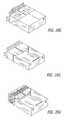
- FIG. 1is a rear isometric view of the fiber-optic module according to a first embodiment of the invention
- FIG. 2is a front isometric view of the fiber-optic module according to the first embodiment of the invention
- FIG. 3is a rear isometric view of a housing/shielding unit according to the first embodiment of the invention.
- FIG. 4Ais a bottom rear isometric view of the housing/shielding unit according to the first embodiment of the invention.
- FIG. 4Bis a bottom rear isometric view of an alternate housing/shielding unit according to an alternate embodiment of the invention.
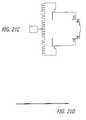
- FIG. 5Ais an isometric view of a module chassis frame and a housing/shielding unit according to the first embodiment of the invention.
- FIG. 5Bis an isometric view of a module chassis frame and a housing/shielding unit according to an alternate embodiment of the invention.
- FIG. 6is an exploded view of the fiber-optic module with the housing/shielding unit and the module chassis frame according to the first embodiment of the invention.
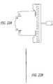
- FIG. 7is an isometric view of a module chassis frame and a housing/shielding unit for an fiber-optic module according to a second embodiment of the invention.
- FIG. 8Ais a front isometric view of a housing/shielding unit according to the second embodiment of the invention.
- FIG. 8Bis a front isometric view of an alternate housing/shielding unit according to an alternate embodiment of the invention.
- FIG. 9Ais a bottom isometric view of the housing/shielding unit according to the second embodiment of the invention.
- FIG. 9Bis a bottom rear isometric view of an alternate housing/shielding unit according to an alternate embodiment of the invention.
- FIG. 10Ais a top exploded view of the second embodiment of the fiber-optic module according to the invention.
- FIG. 10Bis a bottom exploded view of the second embodiment of the fiber-optic module according to the invention.
- FIG. 11Ais a side view of the second embodiment of the fiber-optic module of FIGS. 10A and 10B mounted within a host system.
- FIG. 11Bis a front view of the second embodiment of the fiber-optic module of FIGS. 10A and 10B mounted within a host system (panel 1110 of the host system shown in dashed lines).
- FIG. 12Ais a side view of the first embodiment of the fiber-optic module of FIG. 6 mounted within a host system.
- FIG. 12Bis a front view of the first embodiment of the fiber-optic module of FIG. 6 mounted within a host system (panel 1210 of the host system shown in dashed lines).
- FIG. 13is a perspective view of a host system incorporating embodiments of the fiber-optic modules of the invention.
- FIG. 14illustrates a starting sheet of material for the embodiments of the housing/shielding unit.
- FIG. 15Aillustrates an unfolded flat pattern layout for an embodiment of the housing/shielding unit.
- FIG. 15Billustrates fold and bend lines on the unfolded flat pattern layout of FIG. 15 A.
- FIG. 15Cillustrates an unfolded flat pattern layout for an embodiment of the housing/shielding unit.
- FIG. 15Dillustrates fold and bend lines on the unfolded flat pattern layout of FIG. 15 C.
- FIG. 16Aillustrates an unfolded flat pattern layout for an embodiment of the housing/shielding unit.
- FIG. 16Billustrates fold and bend lines on the unfolded flat pattern layout of FIG. 16 A.
- FIGS. 17A-17Cillustrate alternate methods of assembling a housing/shielding unit with a module chassis frame to form a fiber-optic module.
- FIG. 18Ais a top plan view of a first embodiment of our new design for a one-piece shielded housing
- FIG. 18Bis a right side elevational view thereof, the left side elevational view being a mirror image
- FIG. 18Cis a front elevational view thereof
- FIG. 18Dis a rear elevational view thereof
- FIG. 18Eis a bottom plan view thereof
- FIG. 18Fis a top perspective view thereof.
- FIG. 18Gis a bottom perspective view thereof
- FIG. 19Ais a top plan view of a second embodiment of our new design for a one-piece shielded housing
- FIG. 19Bis a right side elevational view thereof, the left side elevational view being a mirror image
- FIG. 19Cis a front elevational view thereof.
- FIG. 19Dis a rear elevational view thereof.
- FIG. 19Eis a bottom plan view thereof.
- FIG. 19Fis a top perspective view thereof.
- FIG. 19Gis a bottom perspective view thereof.
- FIG. 20Ais a top plan view of a third embodiment of our new design for a one-piece shielded housing
- FIG. 20Bis a right side elevational view thereof, the left side elevational view being a mirror image
- FIG. 20Cis a front elevational view thereof
- FIG. 20Dis a rear elevational view thereof
- FIG. 20Eis a bottom plan view thereof
- FIG. 20Fis a top perspective view thereof.
- FIG. 20Gis a bottom perspective view thereof.
- FIG. 21Ais a top plan view of a first embodiment of our new design of a patterned material layer for a one-piece shielded housing;
- FIG. 21Bis a front elevational view thereof, the rear elevational view being a mirror image
- FIG. 21Cis a bottom plan view thereof
- FIG. 21Dis a right side elevational view thereof, the left side elevational view being a mirror image
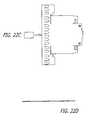
- FIG. 22Ais a top plan view of a second embodiment of our new design of a patterned material layer for a one-piece shielded housing;
- FIG. 22Bis a front elevational view thereof, the rear elevational view being a mirror image
- FIG. 22Cis a bottom plan view thereof
- FIG. 22Dis a right side elevational view thereof, the left side elevational view being a mirror image
- FIG. 23is a top plan view of a third embodiment of our new design of a patterned material layer for a one-piece shielded housing, a bottom plan view being a mirror image and the patterned material layer being a thin and flat sheet so that only the top plan view need be shown.
- FIG. 24is a top perspective view of a fiber optic module for another embodiment of the invention.
- FIG. 25is a bottom perspective view of the fiber optic module of FIG. 24 .
- FIG. 26Ais a rear perspective view of the fiber optic module of FIG. 24 .
- FIG. 26Bis a top view of the fiber optic module of FIG. 24 .
- FIG. 27is a side view of the fiber optic module of FIG. 24 .
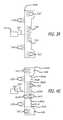
- FIG. 28is a front view of the fiber optic module of FIG. 24 mounted against a faceplate, backplate, or bezel in a system.
- FIG. 29is a side view of the fiber optic module of FIG. 24 mounted in a system.
- FIG. 30is a top view of the fiber optic module of FIG. 24 mounted in a system.
- FIG. 31is a top view of a pattern for a front portion of a shielded housing/cover of the fiber optic module of FIG. 24 .
- FIG. 32is a top view of the pattern of FIG. 31 including bend/fold lines.
- FIG. 33is a top perspective view of a fiber optic module for another embodiment of the invention.
- FIG. 34is a side view of the fiber optic module of FIG. 33 .
- FIG. 35is a top view of the fiber optic module of FIG. 33 .
- FIG. 36is a front view of the fiber optic module of FIG. 33 .
- FIG. 37is a side view of the fiber optic module of FIG. 33 mounted in a system.
- FIG. 38is a top view of the fiber optic module of FIG. 33 mounted in a system.
- FIG. 39is a top view of a pattern for a front portion of a shielded housing/cover of the fiber optic module of FIG. 33 .
- FIG. 40is a top view of the pattern of FIG. 39 including bend/fold lines.
- Fiber-optic modulegenerally refers to fiber-optic transmitter modules, fiber-optic receiver modules, and fiber-optic transceiver modules.
- the various fiber-optic modulescan also be referred to as opto-electronic transmitter, receiver or transceiver modules; and electro-optic transmitter, receiver or transceiver modules.
- the fiber-optic module of the inventionis capable of reducing electromagnetic interference (EMI) from both the fiber-optic module and from the system that incorporates the fiber-optic module.
- EMIelectromagnetic interference
- a fiber-optic modulecomprises a module chassis frame and a housing/shielding unit.
- the housing/shielding unitcan be formed of one piece in which case it can also be referred to as a one-piece integrated housing/shielding unit, a one piece shielded housing, an EMI box or container, or a single-piece shielded housing integrating a protection function and a shielding function.
- the module chassis framecan also be referred to as a chassis, a frame, or a support fixture.
- the housing/shielding unitfunctions both as a protective outer housing for the fiber-optic module as well as an EMI suppression device and a chassis grounding feature.
- the housing/shielding unitcan protect and shield the optical, electrical, and optical-electrical components within a fiber-optic module.
- the housing/shielding unitcan be formed out of conductive materials such as a metal, a plated plastic, a conductive plastic or other electrically conductive material.
- the module chassis framecan be formed of a nonconductive material such as a nonconductive plastic.
- the module chassis framecan also be formed of a conductive material such as sheet metal, a plated plastic, or conductive plastic so as to provide EMI shielding as well.
- the module chassis frameis the central structural support to which components of the fiber-optic module attach. These components can include an opto-electronic transmitter and/or an opto-electronic receiver.
- the fiber-optic moduleincludes a transmitter optical subassembly, a receiver optical subassembly and an electrical subassembly.
- Each of the opto-electronic transmitter and the opto-electronic receiverhas a header which is shielded by a hollow cylindrical shielding collar.
- the hollow cylindrical shielding collarprovides electromagnetic shielding as well.
- the opto-electronic transmittermay include a Vertical Cavity Surface Emitting Laser (VCSEL) or a conventional semiconductor laser mounted inside of the header.
- VCSELVertical Cavity Surface Emitting Laser
- the housing/shieldingis a multi-sided conductive enclosure than can be formed out of sheet metal, plated plastic, conductive plastic or other electrically conductive material.
- sheet metalis etched or stamped to form the housing/shielding unit.
- the housing/shielding unitalso includes a pair of flaps and a septum which allow it to be spot-welded, soldered, glued or otherwise fastened after it is attached to the module chassis frame.
- the housing/shielding unitforms an enclosure that surrounds the module chassis frame. Fingers or tabs extend from the housing/shielding unit to ground it to a bezel, a faceplate, backplate, or a wall of a housing of a host system.
- the fingerspress against the bezel, backplate, faceplate or wall of the housing of the host system to seal electromagnetic radiation therein. In another embodiment, the fingers press against an opening in the bezel, the faceplate, backplate, or the wall of the housing of the host system to seal electromagnetic radiation therein.
- the grounding scheme for the fiber-optic moduleincludes signal grounding and chassis grounding. Two grounds are utilized for isolation to prevent currents induced in the chassis ground from affecting the integrity of signal ground.
- Signal groundis provided through one or more ground pins of a transceiver printed circuit board (PCB) next to the signal pins.
- the one or more ground pinscouple to ground traces on a printed circuit board of the host system.
- Chassis groundis established by coupling to an outer housing of the host system which is electrically isolated from the signal ground.
- the inventionemploys a housing/shielding unit that functions both as protective outer housing as well as an EMI shield or suppression device.
- the housing/shielding unitis a multi-sided enclosure which can be made from one piece or a single piece of sheet metal, plated plastic or other electrically conductive material having an opening at one end for receiving a fiber-optic connector to couple to one or more fiber-optic cables.
- the fiber-optic module 100is a 1 ⁇ 9 fiber-optic transceiver module.
- the fiber-optic moduleis a duplex-SC transceiver designed for use in Gigabit Ethernet applications and is compliant with specifications for IEEE-802.3z Gigabit Ethernet (1000Base-SX) and Class 1 Laser Safety regulations, operates with 50/125 micrometer and 62.5/125 micrometer multimode optical fibers, has an Industry Standard 1 ⁇ 9 Footprint with integral duplex SC connector and meets a mezzanine height standard of 9.8 mm.
- the fiber-optic module 100includes a one-piece or single-piece integrated housing/shielding unit 115 and a module chassis frame 120 .
- the fiber-optic module 100 with the one-piece or single-piece integrated housing/shielding unit 115may also be referred to as a forward shield configuration.
- the housing/shielding unit 115functions both as a housing and as an EMI shield.
- the housing/shielding unit 115minimizes internal electromagnetic radiation from radiating outward and interfering with other electronic circuits and devices. It also minimizes external electromagnetic radiation from radiating inward and interfering with the operation of the fiber-optic module 100 .
- the module chassis frame 120may be formed of a conductive material, such as a conductive plastic, to provide EMI shielding and to support other components assembled thereto.
- the housing/shielding unit 115has a top side 116 , a left side 117 , a right side 118 , and a back side 119 illustrated in FIG. 1.
- a pair of tangs 114 A and 114 Bare present in the back side 119 in order to couple the back side 119 together with the left side 117 and the right side 118 respectively.
- the left side 117 and the right side 118each have a tang 114 A and 114 B bent into an opening of a respective flaps (not shown in FIG. 1 ).
- the housing/shielding unit 115has one or more fingers 112 located near a nose 113 of the fiber-optic module 100 at the edges of a frontal opening 313 .
- the one or more fingerscan also be referred to as tabs.
- the one or more fingersare similarly shaped having a body and a tip which is round in one embodiment.
- the body of the fingers 112are bent outward from the main surface in one embodiment. In an alternate embodiment the tips may be slightly bent from the body of the fingers.
- the fingerscan be equally sized and equally spaced or have different sizing and difference spacing between each. Fingers 112 A are located along an edge of top side 116 of the housing/shielding unit 115 .
- Fingers 112 Bare located along an edge of side 117 of the housing/shielding unit 115 .
- Fingers 112 Care located along an edge of side 118 (not shown in FIG. 1) of the housing/shielding unit 115 .
- Fingers 112 Dare located along an edge of side 119 (not shown in FIG. 1) of the housing/shielding unit 115 .
- Fingers 112 A, 112 B, 112 C and 112 Dare generally referred to as fingers 112 .
- the fingers 112have a forward curvature and are bent outwardly and slightly backwards from a frontal opening in the housing/shielding unit 115 as illustrated.
- the fingers 112can be used to ground the housing/shielding unit 115 by coupling to a bezel or face-plate which is grounded.
- the fingers 112are illustrated as being a plurality of fingers but can be one or more fingers on any one or all sides.
- the fiber-optic module 100includes the housing/shielding unit 115 and the module chassis frame 120 .
- the housing/shielding unitfurther includes a septum (not shown in FIG. 2) and a nose strap 210 .
- the septum and nose strapare folded back into the frontal opening of the housing/shielding unit around the module chassis frame 120 .
- the electrical, optical and electro-optical componentsPrior to folding the septum and nose strap back into the frontal opening, the electrical, optical and electro-optical components are installed on the module chassis frame 120 which is then inserted into the housing 115 in one embodiment, or in another embodiment, the housing is folded around the module chassis frame 120 .
- the nose strap 210 and the septumhold the module chassis frame 120 in place within the housing 115 .
- the module chassis frame 120includes one or more optical connector receptacles 211 with optical connector openings 212 .
- the one or more optical connector receptacles 211are SC optical connector receptacles with the optical connector openings 212 being SC optical connector openings.
- FIG. 3a rear view of the housing/shielding unit 115 is shown.
- the FIGS. 112A, 112 B, 112 C, and 112 Dare located along the edge of the frontal opening 313 of the housing/shielding unit 115 as shown.
- the housing/shielding unit 115is a rectangular box made of sheet metal, plated plastic or any other electrically conductive material. Except for a single side of the housing/shielding unit 115 that is open so that the module chassis frame can be inserted into it, all other sides of the housing/shielding unit can be closed. Once the module chassis frame 120 is inserted into the housing/shielding unit 115 through the open side, it is closed to minimize electromagnetic radiation from the fiber optic module.
- the housing/shielding unit 115has an open region 400 in its bottom side.
- One or more fingers 112 Care located along the edge 419 of the housing/shielding unit 115 .
- the fingers 112curve outward and point more forward from surfaces of the housing/shielding unit.
- the fingers 112have spring-like resilience (i.e. spring loaded or flexible) and provide a mechanical and electrical contact between the fiber-optic module and a bezel, a face-plate or a wall (not shown in FIG. 4 ).
- the fingers 112can also be referred to as spring fingers or forward fingers.
- the housing/shielding unit 115forms an enclosure that surrounds the module chassis frame 120 . Fingers 112 A, 112 B, 112 C, and 112 D can ground the housing/shielding unit 115 to seal in electromagnetic radiation to avoid it affecting a host system, and to avoid the electromagnetic radiation of host system from leaking out through openings in the bezel, faceplate, or backplate.
- FIG. 4Ba bottom left side isometric view of an alternate housing/shielding unit 115 ′ is shown.
- the housing/shielding unit 115 ′differs from housing/shielding unit 115 in the strap, left side, right side, bottom side and the back side.
- the housing/shielding unit 115 ′is additionally longer so that the fingers 112 are nearer the front of the optical connector openings 212 .
- back side 119is replaced by back side 119 ′ with a retaining flap 429 ;
- left side flap 117is replaced by left side flaps 117 A and 117 B separated by a left side slit 1511 L;
- right side flap 118is replaced by right side flaps 118 A and 118 B separated by a right side slit 1511 R;
- bottom side flaps 402 A, 402 B, 405 A and 405 Bare replaced by bottom side flaps 415 A and 415 B;
- strap 210is replaced by strap 210 ′, septum 411 is replaced by septum 411 ′, and open region 400 is replaced by open region 400 ′.
- the housing/shielding unit 115 ′ and the housing/shielding unit 115have similar elements and features including the one or more fingers 112 A, 112 B, 112 C, and 112 D.
- the housing/shielding unit 115 ′forms an enclosure that surrounds the module chassis frame 120 or 120 ′. Fingers 112 A, 112 B, 112 C, and 112 D can ground the housing/shielding unit 115 ′ to seal internal electromagnetic radiation therein to avoid it affecting a host system and keep out external electromagnetic radiation to increase noise immunity of the electronic and opto-electronic components inside. It also minimizes the electromagnetic radiation of the host system from leaking out of openings in the bezel, faceplate, or backplate.
- the module chassis frame 120 ′has a single pin opening 536 in its base 604 ′ through which all pins 612 may extend but otherwise is similar to the module chassis frame 120 .
- the module chassis frame 120 ′includes the optical connector receptacles 211 at one end and a left wall 602 L and a right wall 602 R coupled to the base 604 ′ at an opposite end.
- the walls 6021 and 602 Reach have a slot 634 L and 634 R respectively on their inside surfaces.
- the optical connector receptacles 211have a rectangular opening or slot 626 along the width of the module chassis frame 120 ′.
- the housing/shielding unit 115includes the front nose strap 210 and the septum 411 .
- the front nose strap 210may be a metal or a plastic band used for fastening or clamping the module chassis frame 120 to the housing/shielding unit 115 .
- the front nose strap 210can consists of three portions, a first extension portion 210 A, a wrap portion 210 B and a second extension portion 210 C.
- the wrap portion 210 Bengages with the slot 638 of the module chassis frame 120 or 120 ′.
- the septum 411can also be welded or bonded to bottom flaps of the housing/shielding unit 115 to hold the module chassis frame therein.
- the housing/shielding unit 115 ′includes the front nose strap 210 ′ and the septum 411 ′.
- the front nose strap 210 ′may be a metal or a plastic strap used to fasten or clamp the module chassis frame 120 or 120 ′ to the housing/shielding unit 115 ′.
- the front nose strap 210 ′is a single portion compared to the first extension portion 210 A, wrap portion 210 B and second extension portion 210 C of the front nose strap 210 .
- the nose strap 210 ′engages with the slot 638 of the module chassis frame 120 or 120 ′.
- the septum 411 ′can be welded or bonded to bottom flaps of the housing/shielding unit 115 ′ to hold the module chassis frame therein.
- the fiber-optic module 100includes the integrated one-piece housing/shielding unit 115 , the module chassis frame 120 , and other optical, electrical and opto-electronic components.
- the module chassis frame 120includes the optical connector receptacles 211 at one end and a left wall 602 L and a right wall 602 R coupled to a base 604 at an opposite end.
- the walls 6021 and 602 Reach have a slot 634 L and 634 R respectively on their inside surfaces.
- the optical connector receptacles 211have a rectangular opening or slot 626 along the width of the module chassis frame 120 .
- the base 604has one or more pin openings 636 .
- the optical, electrical and opto-electronic components of the fiber-optic module 100are assembled into the module chassis frame 120 .
- the componentsinclude a printed circuit board (PCB) 610 , a packaged transmitter 620 for transmitting optical signals, a packaged receiver 621 for receiving optical signals, a pair of shielding collars 622 A and 622 B, a pair of SC connectors 650 A and 650 B, and a U-Plate 624 .
- the shielding collars 622 A and 622 Bcan be formed from rolled sheet metal, a plated plastic, a conductive plastic, or other conductive material formed into a hollow cylinder.
- the transmitter 620is an 850-nm VCSEL and the receiver 621 an integrated GaAs PIN preamplifier or PIN-diode.
- the printed circuit board 610includes one or more PCB signal pins 612 , edge traces 614 on each side for straddle mounting the transmitter 620 and the receiver 621 , and integrated circuits 616 for processing signals between the signal pins 612 and the transmitter 620 and the receiver 621 .
- the integrated circuits 616may use a five volt (5 v), a three volt (3 v) or other common power supply voltage used in integrated circuits and host systems.
- the PCB signal pins 612can include a transmit ground pin for transmitter components and a receive ground pin for receiver components. In an alternate embodiment, a single ground pin for electronic components may be provided, isolated from any shielding ground features for the fiber-optic module.
- the printed circuit board (PCB) 610may have a ground plane on its top or bottom surfaces to couple to ground and further provide electromagnetic shielding.
- the module chassis frame 120includes a rectangular opening or slot 626 , a pair of mounting posts 632 extending from its base 604 near left and right sides, slots 634 L and 634 R on inner sides of the walls 602 L and 602 R, one or more pin openings 636 , and one or more optical connector receptacles 211 with one or more optical connector openings 212 .
- the one or more optical connector openings 212is two and the optical connector openings are SC optical connector openings for a duplex SC optical connection.
- the one or more optical connector openings 212is separated by a slot 638 .
- the rectangular opening 626receives the U-plate 624 .
- the one or more pin openings 636receives the one or more PCB signal pins 612 .
- the slots 634 L and 634 Rare press-fit slots and receive the sides of the printed circuit board 610 .
- the pair of mounting posts 632allow the transceiver to be mechanically coupled to a printed circuit board or the like.
- the mounting posts 632can also be connected to chassis ground but should not be connected to signal ground.
- the grounding scheme of the fiber-optic modulecan be divided into categories of signal grounding and chassis grounding.
- the separation of signal grounding from chassis groundingcan keep currents induced in a chassis ground from affecting signal integrity.
- Signal groundis through one or more ground pins of the PCB pins 612 coupled from the PCB 610 to a ground trace in a host printed circuit board.
- the housing/shielding unit 115 or 115 ′is part of the chassis ground and electrically isolated from the signal ground.
- the housing/shielding unit 115 or 115 ′couples to chassis ground of a host system through one or more of the fingers.
- the one or more fingerscouple to a host panel near a host panel opening through which the fiber-optic module may extend.
- the fingerssurround the host panel opening and effectively reduce the size of the opening through which radiated electromagnetic energy may escape to seal the host panel opening through which the fiber-optic module may protrude.
- the housing/shielding unit 115 or 115 ′coupled to chassis ground, it acts as a plug to block EMI radiated emissions from escaping.
- the smaller the host panel openingthe greater the shielding effectiveness as the host system begins to resemble a Faraday cage.
- the packaged transmitter 620may contain a VCSEL or a conventional semiconductor laser and is mounted inside the transmitter port 623 A.
- the packaged receiver 621may include a PIN diode that is mounted inside the receiver port 623 B.
- the transmitter and receiverare each packaged into a TO package and may be referred to as the Tx Header and Rx Header respectively.
- Each of the packaged transmitter 620 and receiver 621have one or more pins or terminals 619 which couple to the edge traces 614 on each side of the printed circuit board 610 to straddle mount them.
- the SC connectors 650 A and 650 Binclude a lens 651 A and 651 B mounted inside ports 623 A and 623 B respectively.
- the portscan also be referred to as TO-can receptacles, TO-can holders, lens holders, etc.
- Semiconductor lasers and/or PINscan be mounted into metal TO-cans, which are then aligned into the ports or receptacles.
- the ports or receptacleshave lenses between the fiber ferrules and the TO-cans. Note that lasers and photodiodes are not required to be packaged in TO-cans and can be packaged in other ways to mate with various shaped ports or receptacles.
- Each of the SC connectors 650 A and 650 Bfurther includes a pair of snap lock clips 652 each having a retaining protrusion 653 , ferrule barrels 654 , support struts 656 in a front portion.
- Each of the SC connectors 650 A and 650 Bfurther includes circular recesses 657 between each of the headers 623 A and 623 B and their respective flanges 655 in a rear portion. Each of the circular recesses 657 mates with the U-shaped openings 627 of the U-plate 624 .
- the transmitter packageis assembled to the SC connector to form the Transmitter Optical Subassembly (Tx OSA).
- This Transmitter Optical Subassemblyis then soldered onto the PCB 610 .
- the pair of shielding collars 622 A and 622 Bare attached with solder to the rear of the ports 623 A and 623 B.
- the PCB 610may be secured by two press-fit slots, one in each inner side of the module chassis frame 120 .
- the U-plate 624provides additional EMI sealing by minimizing leakage through the front of the module.
- the U-plate 624also includes a flap 625 located at its top side.
- the U-plate 624is electrically grounded to the housing/shielding unit 115 by the flap 625 making physical contact with the housing/shielding unit 115 .
- the optical, electro-optical, and the electronic componentsare assembled into the module chassis frame 120 or 120 ′ before the housing/shielding unit 115 encloses it.
- the transmitter 620 and the receiver 621have their pins 619 coupled to the traces 614 T and 614 B of the printed circuit board 610 .
- the pins 619are straddle mounted to the printed circuit board 610 with some pins 619 coupled to the traces 614 T on a top side of the PCB 610 and other pins 619 coupled to the traces 614 B on a bottom side of the PCB 610 . That is, one or more pins mount to one or more traces on one side of the printed circuit board and another one or more pins mount to one or more traces on an opposite side of the printed circuit board.
- the shielding collars 622 A and 622 Bare inserted over the ports 623 A and 623 B of the connectors 650 A and 650 B respectively to provide EMI shielding.
- the TO packaged transmitter 620 and receiver 621are coupled into the ports 623 B and 623 A respectively.
- This forms the optical subassemblywhich is then attached to the electrical components that is in turn coupled into the module chassis frame 120 .
- the front portion of the connectors 650 A and 650 Bare inserted into openings 212 in the nose of the module chassis frame 120 so that the pairs of snap lock clips 652 of each are nearly flush.
- the U-plate 624is inserted into opening 626 so that its U-openings 627 fit into the circular recesses 657 of each respective connector 650 A and 650 B.
- the U-plate 624holds the subassembly of the optical and electrical components coupled into the module chassis frame 120 . Additionally, the U-plate 624 can couple to the shielding collars 622 A and 622 B and the housing/shielding unit 115 or 115 ′. The flap 625 of the U-plate 624 couples to the housing/shielding unit 115 or 115 ′ when the fiber-optic module is fully assembled. This can electrically connect the collars 622 A and 622 B, the U-plate 624 and the housing/shielding unit 115 or 115 ′ together if all are formed of conductive materials.
- grounding the housing/shielding unit 115 or 115 ′ to chassis ground of a host systemcan also couple chassis ground into the U-plate 624 and the shielding collars 622 A and 622 B for electromagnetic shielding externally as well as internally.
- the TO-can headers of the receiver and transmitterare coupled to signal ground or the respective receiver ground and transmitter ground.
- the housing/shielding unit 115 or 115 ′can then be assembled around it. Assembly of the housing/shielding unit 115 or 115 ′ with the module chassis frame 120 or 120 ′ can be performed in different ways.
- the housing/shielding unit 115 or 115 ′can be formed out of a single sheet of material. It can then be folded around the module chassis frame 120 or 120 ′ with the affixed subassembly of optical and electrical components. Alternatively, the housing/shielding unit 115 or 115 ′ can be pre-folded out of the single sheet of material but for one opening at a front or rear end. The module chassis frame 120 or 120 ′ with an affixed subassembly of optical and electrical components can then be inserted into the opening at the front or rear end of the housing/shielding unit 115 or 115 ′.
- the housing/shielding unit 115has all sides pre-folded but for the back side 119 .
- the back side 119is left unfolded so that the module chassis frame 120 can be inserted through a rear opening of the housing/shielding unit 115 .
- a nose end of the module chassis frame 120 and the subassembly of optical and electrical components affixed theretois inserted through the rear opening in the back of the housing/shielding unit 115 with its nose facing forward.
- the back side 119is then folded down to have the tangs 114 A and 114 B bent inward to mate with window openings of flaps coupled to each side 117 and 118 to finish assembly of the housing/shielding unit 115 around the module chassis frame 120 .
- the housing/shielding unit 115has all sides pre-folded but for the septum 411 and strap 210 .
- the septum 411 and strap 210are left unfolded so that the module chassis frame 120 can be inserted through a frontal opening of the housing/shielding unit 115 .
- the septum 411 and strap 210are then folded around the module chassis frame 120 to form the housing/shielding unit 115 .
- a rear end of the module chassis frame 120 and the affixed subassembly of optical and electrical componentsis inserted through the frontal opening of the housing/shielding unit 115 so that the rear faces rearward.
- the septum 411 and strap 210are then folded down and around as illustrated in FIG. 5 to finish assembly of the housing/shielding unit 115 around the module chassis frame 120 .
- all sides of the housing/shielding unit 115are folded around the module chassis frame 120 and its affixed components. These methods of assembly are further described below with reference to FIGS. 14-17C.
- the septum 411is welded, soldered, glued, or otherwise fastened to the pair of flaps 402 A and 402 B as shown in FIG. 4 .
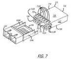
- the housing/shielding unit 715is somewhat similar to the housing/shielding unit 115 but has slightly different dimensions, a few different features and employed in different mounting configurations.
- the housing/shielding unit 715has one or more fingers 712 which are carved out of the surfaces near the perimeter 735 of an open end 739 .
- the one or more fingerscan also be referred to as tabs.
- the one or more fingersare similarly shaped having a body and a tip which is round in one embodiment.
- the body of the fingers 712is bent from the main surface while the tips may be slightly bent from the body to horizontal with the surface.
- the fingers 712have a backwards orientation, originating at the front or nose of the fiber-optic module 700 .
- the one or more fingers 712may also be referred to as backward fingers and the fiber-optic module 700 with the housing/shielding unit 715 may also be referred to as a fiber-optic module with a backward shield configuration.
- the fingers 712can be grouped into fingers 712 A and fingers 712 C located on a top 716 and a bottom 730 respectively of the housing/shielding unit 715 .
- Fingers 712 B and 712 Dare located along the edges of the opening of the housing/shielding unit 715 .
- FIG. 7illustrates six fingers 712 A on a top side 716 and six fingers 712 C on a bottom side 730 , two fingers 712 B on a left side 717 , and two fingers 712 D on a right side 718 , one or more fingers 727 can provide a means of grounding the housing/shielding unit 715 .
- the housing/shielding unit 715differs further from the housing/shielding unit 115 in that it has a different nose strap 710 .
- the strap 710 and the septum 711function similarly to the strap 210 ′ and the septum 411 of the housing/shielding unit 115 ′. Because the dimensions of the housing/shielding unit 715 are larger so that it can extend further forward through an opening, the strap 710 differs significantly from the strap 210 of the housing/shielding unit 115 .
- the housing/shielding unit 715generally has the shape of an oblong box having six sides.
- Front side 738has a frontal opening 739 where the module chassis frame 120 can be inserted.
- the front side 738 of the housing/shielding unit 715includes the septum 710 that is welded or bonded to the flaps 910 A and 910 B.
- the nose strap 711also located at the opening 739 is used for strapping the housing/shielding unit to the module chassis frame 120 .
- FIG. 9Aa bottom isometric view of the housing/shielding unit is shown. Attached to the open end 911 is a front strap 710 shown in the folded down position. Also shown, are two bottom flaps 910 A and 910 B for welding or bonding to septum 711 .
- FIG. 8Ba front view an alternate embodiment of the housing/shielding unit 715 ′ is shown.
- the housing/shielding unit 715 ′generally has a similar shape to the housing/shielding unit 715 .
- the housing/shielding unit 715 ′differs from housing/shielding unit 715 in the left side, right side, bottom side and the back side.
- back side 719is replaced by back side 719 ′ with a retaining flap 429 ;
- left side flap 717is replaced by left side flaps 717 A and 717 B separated by a left side slit 1611 L;
- right side flap 718is replaced by right side flaps 718 A and 718 B separated by a right side slit 1611 R;
- bottom side flaps 910 A and 910 Bare replaced by bottom side flaps 910 A′ and 910 B′.
- the housing/shielding unit 715 ′ and the housing/shielding unit 715have similar elements and features including the one or more fingers 712 A, 712 B, 712 C, and 712 D.
- the housing/shielding unit 715 ′forms an enclosure that surrounds a module chassis frame 120 or 120 ′. Fingers 712 A, 712 B, 712 C, and 712 D can ground the housing/shielding unit 715 ′ to seal in electromagnetic radiation (EMI) to minimize affecting a host system.
- EMIelectromagnetic radiation
- FIG. 9Ba bottom isometric view of the alternate housing/shielding unit 715 ′ is shown. Attached to the open end 911 is a front strap 711 shown in the folded down position. Also shown, are two bottom flaps 910 A′ and 910 B′ for welding or bonding to septum 710 .
- the fiber-optic module 700is a 1 ⁇ 9 fiber-optic transceiver module.
- the fiber-optic module transceivercomplies with the industry standard 1 ⁇ 9 footprint and meets the mezzanine height requirement of 9.8 mm.
- the grounding scheme of the fiber-optic modulecan be divided into categories of signal grounding and chassis grounding.
- the separation of signal ground from chassis groundcan keep currents induced in a chassis ground from affecting signal integrity.
- Signal groundis through one or more ground pins of the PCB pins 612 coupled from the PCB 610 to a ground trace in a host printed circuit board.
- the housing/shielding unit 715 or 715 ′is part of the chassis ground and electrically isolated from the signal ground.
- the housing/shielding unit 715 or 715 ′couples to chassis ground of a host system through one or more of the fingers 712 .
- the one or more fingers 712couple to a host panel near a host panel opening through which the fiber-optic module may extend.
- the fingers 712contact the host panel opening and effectively reduce the size of the opening through which radiated electromagnetic energy may escape to seal the host panel opening through which the fiber-optic module may protrude.
- the housing/shielding unit 715 or 715 ′coupled to chassis ground, it acts as a plug to block EMI radiated emissions from escaping.
- the smaller the host panel openingthe greater the shielding effectiveness as the host system begins to resemble a Faraday cage.
- the fiber-optic module 700 of the inventionincludes a housing/shielding unit 715 or 715 ′, and a module chassis frame 120 or 120 ′.
- the optic, electronic, and opto-electronic components of the fiber-optic moduleare placed into the module chassis frame 120 . These components and their assembly were previously described with reference to FIG. 6 and the fiber-optic module 100 and are not repeated again for brevity.
- the housing/shielding unit 715 or 715is assembled around the module chassis frame and the optic, electronic, and opto-electronic components affixed thereto, it can couple to the flap 625 of the U-plate 624 so that it an be electrically grounded to chassis ground.
- the U-plate 624can couple to the shielding collars 622 A and 622 B. This can electrically connect the collars 622 A and 622 B, the U-plate 624 and the housing/shielding unit 715 or 715 ′ together if all are formed of conductive materials. Assuming they are electrically connected, grounding the housing/shielding unit 715 or 715 ′ to chassis ground of a host system can also couple chassis ground into the U-plate 624 and the shielding collars 622 A and 622 B for electromagnetic shielding externally as well as internally.
- the housing/shielding unit 715 or 715 ′can then be assembled around it. Assembly of the housing/shielding unit 715 or 715 ′ around the module chassis frame 120 can be performed in the same ways previously described for the housing/shielding unit 115 or 115 ′.
- the fiber-optic module 700includes a backward shield which is provided by the one-piece or single-piece integrated housing/shielding unit 715 or 715 ′.
- the fiber-optic module 700 with the one-piece or single-piece integrated housing/shielding unit 715 or 715 ′provides an extended mount as illustrated by its nose extending beyond a bezel, faceplate, or backplate.
- the host systemmay be a hub, switch, bridge, server, personal computer, or other network or electronic equipment desiring to connect to a communication system using an fiber-optic module.
- the fiber-optic module 700is coupled to a printed circuit board 1130 within the host system.
- a bezel, faceplate, or backplate 1110 of the host systemhas a transceiver opening 1112 through which the nose of the fiber-optic module extends when its coupled to the host system.
- the transceiver opening 1120 of the bezel 1110is sized to appropriately mate with the fingers 712 of the fiber-optic module 700 .
- the opening 1120has an inner surface 1114 which mates with the fingers 712 to make an electrical coupling. By making contact to the inner surface 1114 , a backside surface of the bezel 1110 can be insulated to avoid shorting an electrical component that might make contact thereto.
- the fingers 712compress towards the fiber-optic module when mating with the inner surface 1114 and expand outward to form a tight mechanical fit and a reliable electrical connection.
- the expansion of the fingers 712 outwardeffectively make the opening 1120 smaller through which radiated electromagnetic energy might otherwise escape.
- the fingers 712also deter the nose of the fiber-optic module 700 from extending excessively out through the opening 1120 of the bezel 1110 .
- the housing/shielding unit 715 of the fiber-optic modulecan be grounded by one or more fingers 712 coupling to the inner surface 1114 of the opening 1120 .
- the housing/shielding unit 715 of the transceiver 700can be grounded through a pin or other connection coupled to the PCB 1130 of the host system.
- FIGS. 12A and 12Ba magnified side view and a magnified frontal view of the fiber-optic module 100 within a host system is illustrated.
- the host systemmay be a switch, bridge, a server, personal computer, or other network or electronic equipment desiring to connect to a communication system using an fiber-optic module.
- the fiber-optic module 100is coupled to a printed circuit board 1130 within the host system.
- a bezel, faceplate, or backplate 1210 of the host systemhas a transceiver opening 1220 through which the nose of the fiber-optic module partially extends when coupled to the host system.
- the fiber-optic module 100a forward shield configuration with the one-piece or single-piece integrated housing/shielding unit 115 or 115 ′, provides a flush mount as illustrated by FIG. 12 A.
- the transceiver opening 1220 of the bezel 1210is sized appropriately to allow insertion of a fiber-optic connector into the fiber-optic module 100 .
- the bezel, faceplate, or backplate 1210 of the host systemhas a backside surface 1214 to which the fingers 112 can make an electrical and a mechanical coupling. Furthermore, the fingers 112 deter the EMI of both the fiber-optic module 100 and the host system board 1130 from extending excessively out through the transceiver opening 1212 of the bezel 1210 .
- the housing/shielding unit 115 of the fiber-optic module 100can be grounded by one or more fingers 112 coupling to the back side surface 1214 of the bezel 1210 .
- the housing/shielding unit 115 or 115 ′ of the fiber-optic module 100can be grounded through a pin or other grounding feature that is coupled to a chassis ground trace of the PCB 1130 of the host system commonly coupled to the bezel.
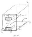
- an exemplary host system 1300having the fiber-optic module 100 and the fiber-optic module 700 .
- the host system 1300has a bezel, a faceplate or a host panel 1310 with opening 1120 and opening 1220 for the fiber-optic module 700 and the fiber-optic module 100 respectively.
- the fiber-optic module 700is coupled to host printed circuit board 1130 .
- the fiber-optic module 100is coupled to host printed circuit board 1130 ′.
- the host printed circuit boards 1130 and 1130 ′may include a ground plane on a top surface or bottom surface under the area of the fiber optic module 100 and 700 in order to provide additional electromagnetic shielding.
- the host system 1300begins to resemble a Faraday cage.
- the housing/shielding unit 115 , 115 ′, 715 , 715 ′effectively seals openings 1120 and 1220 in the host panel 1310 to deter electromagnetic radiation from leaking into or out of the host system.
- the one or more fingers 112 of the housing/shielding unit 115 or 115 ′can surround the opening 1220 .
- the one or more fingers 112 of the housing/shielding unit 115 or 115 ′can expand into the opening 1120 . With the housing/shielding unit 115 or 115 ′ coupled to chassis ground, it acts as a plug to block EMI radiated emissions from escaping.
- the fiber-optic modules 100 and 700are designed to perform to these specified limits of EMI including complying with FCC Class B limits.
- the fiber-optic modules 100 and 700are also designed to provide good noise immunity from externally generated radio-frequency electromagnetic fields.
- EMCelectromagnetic compliance
- the internal shieldsshields 622 A and 622 B and the U-Plate 624
- the fiber-optic modules 100 and 700are further designed to meet Class 1 eye safety and comply with FDA 21CFR1040.10 and 1040.11 and the IEC 825-1.
- FIGS. 14-17Cmethods of forming the housing/shielding units 115 ′ and 715 ′ out of a sheet of a material layer and assembly with the module chassis frame 120 or 120 ′ is illustrated.
- FIG. 14a starting sheet of a layer of material 1400 for the housing/shielding units 115 , 115 ′, 715 and 715 ′ is illustrated.
- the sheet of material 1400is a conductive material and can be a metal, a plated plastic, a conductive plastic or other known type of electrically conductive material.
- a first step in the processis to stamp, etch or cut the patterns for the housing/shielding unit 115 , 115 ′, 715 or 715 ′ out of the sheet of material 1400 .
- the unfolded flat pattern layout 1500is a patterned material layer for the housing/shielding unit 115 ′ formed out of the starting sheet of the layer of material 1400 .
- the forward fingers 112 , tangs 114 A and 114 B, strap 210 and the septum 411 ′ of the housing/shielding unit 115 ′are easily discernable.
- a pair of left and right window openings 1522 L and 1522 Rare also visible in the unfolded flat pattern layout 1500 .
- fold/bend linesare illustrated on the unfolded flat pattern layout 1500 to form the housing/shielding unit 115 ′.
- a slightly alternate pattern and alternate fold/bend linescan be utilized to form the housing/shielding unit 115 .
- the fold/bend lines illustrated on the unfolded flat pattern layout 1500make other features and components of the housing/shielding unit 115 ′ discernable.
- left flap and right flap fold lines 1502 L and 1502 Rinclude left flap and right flap fold lines 1502 L and 1502 R, a back flap fold line 1504 , left and right tang fold lines 1505 L and 1505 R, a retaining flap fold line 1506 , left wing and right wing fold lines 1508 L and 1508 R, finger base bend line 1512 , left bottom flap and right bottom flap fold lines 1514 L and 1514 R, a strap fold line 1516 , and a septum fold line 1517 .
- a left wing 1520 L and a right wing 1520 Rinclude tang window openings 1522 L and 1522 R respectively.
- the tangs 114 A and 114 Bmate with the tang window openings 1522 L and 1522 R respectively to hold the left wing and right wing coupled to the back side 119 ′ after folding.
- the septum 411 ′is coupled to the right bottom flap 415 A and the left bottom flap 415 B with an adhesive or a weld to hold the housing/shielding unit and the module chassis frame assembled together.
- the left wing fold line 1508 Ldefines the left wing 1520 L from the left side flap 117 B.
- the right wing fold line 1508 Rdefines the right wing 1520 R from the right side flap 118 B.
- the right side fold line 1502 R and the right side slit 1511 Rdefines right flaps 118 A and 118 B from the top side 116 .
- the left side fold line 1502 L and the left side slit 1511 Ldefines left flaps 117 A and 117 B from the top side 116 .
- the right bottom flap fold line 1514 Rdefines the right bottom flap 415 A.
- the left bottom flap fold line 1514 Ldefines the left bottom flap 415 B.
- the retaining flap fold line 1506defines a retaining flap 429 coupled to the back side flap 119 ′.
- the fold/bend lines illustrated on the unfolded flat pattern layout 1500are folded and/or bent to form the housing/shielding unit 115 ′ as illustrated in FIG. 4 B.
- the folds along fold linesare made at nearly a ninety degree angle but for the fold lines of the tangs 114 A and 114 B and fingers.
- the fingers 112may be first bent or lastly bent to curve outward along the bend lines 1512 .
- the left flaps 117 A and 117 B and the right flaps 118 A and 118 Bmay be the next to be folded or they may be the first to be folded along fold lines 1502 L and 1502 R.
- the right bottom flap 415 A and the left bottom flap 415 Bare next folded along the right bottom flap fold line 1514 R and the left bottom flap fold line 1514 L respectively.
- the next sequence of fold/bend stepscan depend upon the method of assembly of the fiber-optic module utilized.
- the front of the housing/shielding unit 115 ′is assembled first.
- the septum 411 ′is folded along fold line 1517 and then the strap 210 ′ is folded along fold line 1516 .
- the left wing 1520 L and the right wing 1520 Rbeing folded along the left wing fold line 1508 L and the right wing fold line 1508 R respectively;
- the back side flap 119 ′being folded along the fold line 1504 ;
- the tangs 114 A and 114 Bbeing folded along fold lines 1505 L and 1505 R respectively;
- the retaining flap 429being folded along the retaining flap fold line 1506 .
- the rear of the housing/shielding unit 115 ′is assembled first.
- the left wing 1520 L and the right wing 1520 Rare folded along the left wing fold line 1508 L and the right wing fold line 1508 R respectively;
- the back side flap 119 ′is folded along the fold line 1504 ;
- the tangs 114 A and 114 Bare folded along fold lines 1505 L and 1505 R respectively;
- the retaining flap 429is folded along the retaining flap fold line 1506 .
- the septum 411 ′being folded along fold line 1517 and then the strap 210 ′ folded along fold line 1516 .
- either order of assembly in the first or second casecan be utilized or mixed together.
- the one or more fingers 112may alternately be bent outward from a frontal opening the into their curved shape as a last step in the folding/bending process.
- a slightly alternate pattern of the layout 1500 with alternate fold/bend linesis utilized to fold and bend into shape to form the housing/shielding unit 115 as illustrated in FIGS. 1-3, 4 A, 5 and 12 A.
- the unfolded flat pattern layout 1500is a patterned material layer for the housing/shielding unit 115 formed out of the starting sheet of the layer of material 1400 .
- the forward fingers 112 , tangs 114 A and 114 B, strap 210 and a septum 411 of the housing/shielding unit 115are easily discernable.
- the pair of left and right window openings 1522 L and 1522 Rare also visible in the unfolded flat pattern layout 1500 ′.
- fold/bend linesare illustrated on the unfolded flat pattern layout 1500 ′ to form the housing/shielding unit 115 .
- the fold/bend lines illustrated on the unfolded flat pattern layout 1500 ′make other features and components of the housing/shielding unit 115 discernable.
- 15Dinclude left flap and right flap fold lines 1502 L′ and 1502 R′, a back flap fold line 1504 , left and right tang fold lines 1505 L and 1505 R, left wing and right wing fold lines 1508 L and 1508 R, finger base bend line 1512 , left bottom flap and right bottom flap fold lines 1514 L′ and 1514 R′, a first strap fold line 1516 ′, and a second strap fold line 1517 ′.
- the fold bend lines of the unfolded flat pattern layout 1500 ′are similar to the fold/bend lines of the unfolded flat pattern layout 1500 but for left flap and right flap fold lines 1502 L′ and 1502 R′, left bottom flap and right bottom flap fold lines 1514 L′ and 1514 R′, a first strap fold line 1516 ′, and a second strap fold line 1517 ′.
- the right side fold line 1502 R′defines the right flap 118 from the top side 116 .
- the left side fold line 1502 L′defines left flap 117 from the top side 116 .
- the right bottom flap fold line 1514 R′defines the right bottom flaps 402 A and 405 A.
- the left bottom flap fold line 1514 L′defines the left bottom flaps 402 B and 405 B.
- the back fold line 1504defines the back side flap 119 from the top side 116 .
- the first strap fold line 1516 ′ and the second strap fold line 1517 ′define the first extension portion 210 A, the wrap portion 210 B and the second extension portion 210 C of the strap 210 .
- the strap 210is folded along the first strap fold line 1516 ′ and the second strap fold line 1517 ′.
- the septum 411can couple to the right bottom flaps 402 A and 405 A and the left bottom flaps 402 B and 405 B with an adhesive or a weld to hold the housing/shielding unit and the module chassis frame assembled together.
- the fold/bend lines illustrated on the unfolded flat pattern layout 1500 ′are folded and/or bent to form the housing/shielding unit 115 as illustrated in FIGS. 1, 2 , 3 , and 4 A.
- the folds along fold linesare made at nearly a ninety degree angle but for the fold lines of the tangs 114 A and 114 B and fingers 112 .
- the fingers 112may be first bent or lastly bent to curve outward along the bend lines 1512 .
- the left flap 117 and the right flap 118may be the next to be folded or they may be the first to be folded along fold lines 1502 L′ and 1502 R′.
- the right bottom flaps 402 A and 405 A and the left bottom flaps 402 B and 405 Bare next folded along the right bottom flap fold line 1514 R′ and the left bottom flap fold line 1514 L′ respectively.
- the next sequence of fold/bend stepscan depend upon the method of assembly of the fiber-optic module utilized. These were previously described with reference to the unfolded flat pattern layout 1500 of FIG. 15 B.
- the unfolded flat pattern layout 1600is a patterned material layer for the housing/shielding unit 715 ′ formed out of the starting sheet of the layer of material 1400 .
- the backward fingers 712 , tangs 114 A and 114 B, strap 710 and the septum 711 of the housing/shielding unit 715 ′are easily discernable.
- a pair of left and right window openings 1622 L and 1622 Rare also visible in the unfolded flat pattern layout 1600 .
- fold/bend linesare illustrated on the unfolded flat pattern layout 1600 to form the housing/shielding unit 715 ′.
- a slightly alternate pattern and alternate fold/bend linescan be utilized to form the housing/shielding unit 715 .
- the fold/bend lines illustrated on the unfolded flat pattern layout 1600make other features of the housing/shielding unit 715 ′ discernable.
- the fold/bend lines illustrated in FIG. 16Binclude left flap and right flap fold lines 1602 L and 1602 R, back flap fold line 1604 , left and right tang fold lines 1605 L and 1605 R, retaining flap fold line 1606 , left wing and right wing fold lines 1608 L and 1608 R, finger base bend line 1612 B, finger tip bend line 1612 T, left bottom flap and right bottom flap fold lines 1614 L and 1614 R, strap fold line 1616 , septum fold line 1617 .
- the folds along fold linesare made at nearly a ninety degree angle but for the fold lines of the tangs 114 A and 114 B and fingers.
- a left wing 1620 L and a right wing 1620 Rinclude window openings 1622 L and 1622 R respectively.
- the tangs 114 A and 114 Bmate with the window openings 1622 L and 1622 R respectively to hold the left wing and right wing coupled to the back side 719 ′ after folding.
- the left wing fold line 1608 Ldefines the left wing 1620 L from the left side flap 717 B.
- the right wing fold line 1608 Rdefines the right wing 1620 R from the right side flap 718 B.
- the right side fold line 1602 R and the right side slit 1611 Rdefines right flaps 718 A and 718 B from the top side 716 .
- the left side fold line 1602 L and the left side slit 1611 Ldefines left flaps 717 A and 717 B from the top side 716 .
- the right bottom flap fold line 1614 Rdefines the right bottom flap 910 A′.
- the left bottom flap fold line 1614 Ldefines the left bottom flap 910 B′.
- the retaining flap fold line 1606defines a retaining flap 1626 coupled to the back side flap 719 ′.
- the fold/bend lines illustrated on the unfolded flat pattern layout 1600are respectively folded and/or bent to form the housing/shielding unit 715 ′ as illustrated in FIGS. 8B and 9B.
- the sequence of folding and bending of the fold lines in the unfolded flat pattern layout 1600is similar to that of the unfolded flat pattern layout 1500 but for the fingers.
- the fingers 712 for the housing/shielding unit 715 ′ or 715are generally easier to push or pull out of the surface of the unfolded flat pattern layout 1600 first. Then, the sequence of folding and bending can proceed similarly for any of the three methods of assembly previously described.
- FIGS. 17A-17Cmethods of assembly of the housing/shielding units 115 and 715 with the module chassis frame 120 is illustrated.
- the layout 1500 or 1600are placed on top of the module chassis frame 120 .
- Folding and bendingis then performed around the module chassis frame 120 or 120 ′ along the fold lines and bend lines described in FIGS. 15A-15B or 16 A- 16 B respectively to form the housing/shielding unit 115 , 115 ′, 715 or 715 ′.
- the housing/shielding unit 115 , 115 ′, 715 or 715 ′then surrounds the module chassis frame 120 or 120 ′.
- the tangs 114 A and 114 Bare then folded into the window openings 1522 L and 1522 R or 1622 L and 1622 R. This results in a substantially complete fiber-optic module such as fiber-optic module 100 illustrated in FIG. 1 for example.
- the layout 1500 or 1600is first folded and bent along the fold lines and bend lines described in FIGS. 15A-15B or 16 A- 16 B respectively but for fold lines 1516 and 1517 or 1616 and 1617 .
- the module chassis frame 120 or 120 ′ with the affixed componentsis inserted into the frontal opening with its rear entering first. Then the strap 210 , 210 ′ or 710 and the septum 411 or 711 are then folded fold lines 1516 and 1517 or 1616 and 1617 as described in FIGS. 15A-15B and FIG.
- the septum 411 or 711is affixed in place by being welded by spot welding, soldered with a solder, glued with an adhesive or otherwise fastened to a pair of bottom flaps. This results in a substantially complete fiber-optic module such as fiber-optic module 100 illustrated in FIG. 1 for example.
- the layout 1500 or 1600is first folded and bent along the fold lines and bend lines described in FIGS. 15A-15B or 16 A- 16 B respectively but for fold lines 1504 , 1505 L, 1505 R, 1506 , 1508 L and 1508 R or 1604 , 1605 L, 1605 R, 1606 , 1608 L and 1608 R.
- the septum 411 or 711is affixed in place by glue or welding. This leaves the rear of the housing/shielding unit 115 , 115 ′, 715 or 715 ′ open without the back side flap 119 ′ or 719 ′ and the left and right wings 1520 L or 1620 L and 1520 L or 1620 R being folded.
- the front end of the module chassis frame 120 or 120 ′ with the affixed componentsis inserted into the rear opening of the housing/shielding unit, nose first.
- the left and right wings 1620 L and 1620 Rare then folded followed by back side flap 119 ′ or 719 ′ along fold lines 1504 , 1506 , 1508 L and 1508 R or 1604 , 1606 , 1608 L and 1608 R as shown and described in FIGS. 15A-15B or 16 A- 16 B respectively.
- the tangs 114 A and 114 Bare then folded along fold lines 1505 L and 1505 R or 1605 L and 1605 R into the openings 1522 L and 1522 R or 1622 L and 1622 R respectively.
- the housing/shielding unit 115 , 115 ′, 715 or 715 ′is held around the module chassis frame 120 or 120 ′. This results in a substantially complete fiber-optic module such as fiber-optic module 100 illustrated in FIG. 1 for example.
- Fingers of a housing/shielding unitcan deter electromagnetic radiation from leaking out of the opening by expanding and/or surrounding one or more portions of the opening or expanding into host tabs as will be illustrated below. In either case the fingers of the housing/shielding unit can make a connection to ground for the shielded housing/cover.
- Fiber optic module 2400includes a shielded housing/cover 2415 as well as other elements previously described in reference to fiber optic modules 100 , 100 ′, 700 or 700 ′.
- the shielded housing/cover 2415maybe an integrated one-piece housing/cover or a two-piece housing/cover.
- the shielded housing/coverincludes a front-shielded housing/cover 2415 A and rear shielded housing/cover 2415 B.
- the rear shielded housing/cover 2415 Boverlaps a portion of the front-shielded housing/cover 2415 A.
- the front shielded housing/cover 2415 Acould overlap a portion of the rear housing/cover 2415 B.
- the fiber optic module 2400provides forward fingers on the perimeter of the top and bottom of the nose and backward fingers in the sides near the nose and the perimeter of the shielded housing 2415 .
- Shielded housing/cover 2415includes forward fingers 112 A′ on the top side near the perimeter, forward fingers 112 C′ on the bottom side near the perimeter, backward fingers 712 B′ in the left side, and backward fingers 712 D′ in the right side near the perimeter.
- the shielded housing 2415includes a front top side 2416 A, a rear top side 2416 B, a front left side 2417 A, a rear left side 2417 B, a backside 2419 , a front right side 2418 A, and a rear right side 2418 B.
- the shielded housing/cover 2415also includes a strap 210 ′ and a septum 411 ′.
- Fiber optic module 2400includes the chassis/base 120 or 120 ′.
- the chassis or base 120 or 120 ′includes vent openings 633 on the bottom side thereof.
- the left side 2417 B of the shielded housing/cover 2415meets the backside 2419 of the shielded housing/cover 2415 at a corner which may use a tongue and groove coupling 2430 .
- the rear portion 2415 B of the shielded housing/cover 2415can include a back edge wrap 2429 B, a left edge wrap 2429 L and a right edge wrap 2429 R.
- one or more of the edge wrapscan wrap around chassis/base 120 or 120 ′ to couple them together.
- the front portion of the shielded housing/cover 2415 Aincludes a right side bottom flap 415 A and a left side bottom flap 415 B.
- the right side bottom flap 415 A and the left side bottom flap 415 B of the shielded housing/covercan be formed around chassis/base 120 or 120 ′ to couple them together.
- the septum 411 ′can be overlapped by the left and right side bottom flap 415 A and 415 B.
- the forward fingers 112 A′ and 112 C′ and the backward fingers 712 B′ and 712 D′can be formed out of different shapes including round fingertips, rectangular fingertips, or triangular fingertips.
- the fingersmaybe arched shaped or curved or bent in one or more places, in order to provide spring pressure and expand outward to seal around an opening in an enclosure, faceplate, or bezel for input/output connections.
- the shielded housing/cover 2415can be an integrated one piece or a two-piece design.
- the shielded housing 115 , 115 ′, 715 and 715 ′can be either an integrated one-piece or a two-piece shielding housing/cover having a front portion and a rear portion.
- the same rear portion 2415 B of the shielded housing/covermaybe used interchangeably with different front portions, such as the front portion 2415 A of the shielded housing/cover 2415 . That is, by simply changing the front portion of the shielded housing/cover, backward fingers maybe supplied on top, bottom, left and right sides or forward fingers maybe provided on left, right, top and bottom sides or any combination thereof.
- backward fingersmaybe supplied on top, bottom, left and right sides or forward fingers maybe provided on left, right, top and bottom sides or any combination thereof.
- Thisallows flexible assembly of fiber optic modules.
- the decision of the type of shielding for the fiber optic modulecan be postponed until the subassembly of the chassis is completed and the rear portion of the shielded housing is wrapped around it.
- the front portion of the shielded housing/coverbeing interchangeable, allows flexibility in manufacturing and meeting the demands of customers.
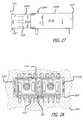
- a rear perspective view of the fiber optic module 2400illustrates the forward fingers 112 A′ having rounded tips while the backward fingers 712 B′ have more of a triangular shaped tip.
- a top view of the fiber optic module 2400illustrate differences in the positions of the forward fingers 112 A′ and 112 C′ and the backward fingers 712 B′ and 712 D′ in the front portion 2415 A of the shielded housing/cover 2415 .
- the forward fingersmay be curved or bent in differing places.
- the front shielded housing/cover 2415 Aincludes the forward fingers 112 A′ on a top side and the forward fingers 112 C′ on a bottom side.
- the forward fingers 112 A′are illustrated as being curved or arched shaped in FIG. 27 .
- the forward fingers 112 C′are illustrated as being bent in two places (i.e. bent shaped) in FIG. 27 but can take on a curved or arched shape or other bent configuration in order to make contact with a back side surface of a bezel, faceplate, or backplate.
- the forward fingers 112 A′can take on a bent shape or other bending configuration in order to make contact to a back side surface of a bezel, faceplate, or backplate.
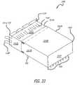
- a front view of the fiber optic module 2400is illustrated mounted adjacent a bezel, faceplate, or backplate 2810 .
- the bezel, faceplate, or backplate 2810includes an opening 2820 to allow a fiber optic plug to be inserted into the fiber optic module 2400 .
- Duplex SC receptacles for duplex SC plugsprovided in one embodiment, can be readily seen in the front view of the fiber optic module 2400 separated by the strap 210 ′.
- the forward fingers 112 A′ and 112 C′couple (i.e. press) against the backside surface of the bezel, faceplate, or backplate 2810 adjacent to the opening 2820 without coupling into the opening 2820 . That is, the forward fingers 112 A′ and 112 C′ are not inserted into the opening 2820 .
- the left and right side backward fingers 712 B and 712 B′also do not couple into the opening 2820 nor do they couple against the backside surface of the bezel, faceplate, or backplate 2810 . Rather, the backside backward fingers 712 B and 712 B′ couple to host tabs (not shown in FIG. 28 ).
- the host tabscan be integrated or coupled to the bezel, faceplate, or backplate 2810 .
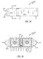
- FIG. 29a cutaway side view of the fiber optic module 2400 inserted into a host system 2900 is illustrated.
- the fiber optic module 2400couples to a host printed circuit board 1130 or 1130 ′.
- the top forward fingers 112 A′ and the bottom forward fingers 112 C′couple to a backside surface 2902 of the bezel, faceplate, or backplate 2810 as illustrated in FIG. 29 .
- the top forward fingers 112 A′ and the bottom forward fingers 112 C′do not couple to an inside surface 2902 of the opening 2820 .
- Neither do the backward fingers 712 D′couple into the opening 2820 .
- the backward fingers 712 D′(as well as the backward fingers 712 B′) are offset from the opening 2820 and the backside surface 2902 of the bezel, faceplate, or backplate 2810 .
- the host system 2900includes a left side host tab 3010 B and a right side host tab 3010 A.
- the right side backward fingers 712 D′couple to an inside surface 3014 A of the host tab 3010 A.
- the left side backward fingers 712 B′couple to an inside surface 3014 B of the host tab 3010 B.
- the host tabs 3010 A and 3010 Bextend along the sides of the front shielded housing/cover 2415 A. The overlap may provide improved EMI performance in deterring electromagnetic radiation from leaking in and out of the opening 2820 .
- the host tabs 3010 A and 3010 Bmay additionally provide lateral support when optical plugs are pushed into and pulled out of for the fiber optic module 2400 , while the printed circuit board 1130 or 1130 ′ provides horizontal support.
- the host tabs 3010 A and 3010 Bmay be coupled to the backside 2902 of the bezel, faceplate, or backplate 2810 .
- the host tabs 3010 A and 3010 Bmay be integrally formed with the bezel, faceplate, or backplate 2810 and extend backward from the backside 2902 .
- the top forward fingers 112 A′ and the bottom forward fingers 112 C′do not couple to the host tabs 3010 A and 3010 B.
- the fiber optic module 2400can have its nose flush with the faceplate 2810 .
- FIG. 31an unfolded flat pattern layout of the front portion 2415 A (i.e., the front shielded housing/cover) of the shielded housing 2415 is illustrated.
- the rear shielded housing/cover 2415 Bcan be envisioned by slightly modifying FIG. 16B so that the slits 1611 L and 1611 R cut through the top 716 to meet each other.
- the unfolded flat pattern layout 2415 Ais a patterned material layer formed out of the starting sheet of the layer of material 1400 .
- the front shielded housing/cover 2415 A and the rear shielded housing/cover 2415 Bcan be stamped, cut or etched out of a conductive material (i.e. a metal such as stainless steel for example).
- the forward fingers 112 A′ and 112 C′ and the backward fingers 712 B′ and 712 D′can be formed out of different shapes including round fingertips, rectangular fingertips or triangular fingertips.
- fold/bend linesare illustrated on the unfolded flat pattern layout of the front shielded housing/cover 2415 A.
- the fold/bend lines illustrated on the unfolded flat pattern layoutmake other features of the front shielded housing/cover 2415 A discernable.
- the fold/bend lines illustrated in FIG. 32include left flap and right flap fold lines 3202 L and 3202 R, left bottom flap and right bottom flap fold lines 3214 L and 3214 R, the forward finger base bend line 1512 , the backward finger base bend line 1612 B, the finger tip bend line 1612 T, the strap fold line 1616 , and the septum fold line 1617 .
- the folds along fold linesare made at nearly a ninety degree angle but for the bend lines of the fingers 112 A′, 112 C′, 712 B′, and 712 D′.
- the right bottom flap fold line 3214 Rdefines the right bottom flap 415 A.
- the left bottom flap fold line 3214 Ldefines the left bottom flap 415 B.
- the right side fold line 3202 R and the right bottom flap fold line 3214 Rdefine the front right side 2418 A.
- the left side fold line 3202 L and the left bottom flap fold line 3214 Ldefine the front left side 2417 A.
- the left flap and right flap fold lines 3202 L and 3202 Rdefine the front top side 2416 A.
- the fold/bend lines illustrated on the unfolded flat pattern layout of FIG. 32are respectively folded and/or bent to form the front shielding/cover 2415 A as illustrated in FIGS. 24-30.
- the sequence of folding and bending of the fold lines in the unfolded flat pattern layout of the front shielded housing/cover 2415 Ais similar to that of the unfolded flat pattern layouts 1500 and 1600 but for the fingers.
- the backward fingers 712 B′ and 712 D′can be first pushed or pulled out of the surface of the unfolded flat pattern layout. Then, the sequence of folding and bending can proceed on the front shielded housing/cover 2415 A.
- the forward fingers 112 A′ and 112 C′ and the backward fingers 712 B′ and 712 D′may be arched shaped or curved or bent in one or more places, in order to provide spring pressure and expand outward to seal around the opening 2820 and/or couple to the host tabs 3010 A and 3010 B.
- Fiber optic module 3300includes a shielded housing/cover 3315 as well as other elements previously described in reference to fiber optic modules 100 , 100 ′, 700 , 700 ′ and 2400 .
- the shielded housing/cover 3315maybe an integrated one-piece housing/cover or a two-piece housing/cover.
- the shielded housing/coverincludes a front-shielded housing/cover 3315 A and rear shielded housing/cover 3315 B.
- the rear shielded housing/cover 3315 Boverlaps a portion of the front-shielded housing/cover 3315 A in one embodiment.
- the front shielded housing/cover 3315 Acould overlap a portion of the rear housing/cover 3315 B in another embodiment.
- the fiber optic module 3300provides forward fingers on the perimeter of the left and right sides of the nose and backward fingers in the top and bottom near the nose and the perimeter of the shielded housing 3315 .
- shielded housing/cover 3315includes backward fingers 712 A′ in the top side near the perimeter, backward fingers 712 C′ in the bottom side near the perimeter (not shown in FIG. 33 ), forward fingers 112 B′ in the left side, and forward fingers 112 D′ in the right side near the perimeter.
- the shielded housing 3315includes a front top side 3316 A, a rear top side 3316 B, a front left side 3317 A, a rear left side 3317 B, a backside 3319 , a front right side 3318 A, and a rear right side 3318 B.
- the shielded housing 3315also includes a strap 210 ′ and a septum 411 ′ as is shown in FIG. 25 of the shielded housing 2415 .
- Fiber optic module 3300includes the chassis/base 120 or 120 ′ and the optical, opto-electronic, and the electronic components assembled therein.
- the chassis or base 120 or 120 ′includes vent openings 633 on the bottom side thereof.
- the left side 3317 B of the shielded housing/cover 3315meets the backside 3319 of the shielded housing/cover 3315 at a corner which may use a tongue and groove coupling.
- the rear portion 3315 B of the shielded housing/cover 3315can include a back edge wrap, a left edge wrap and a right edge wrap. When assembled with chassis/base 120 or 120 ′ one or more of the edge wraps can wrap around chassis/base 120 or 120 ′ to hold them assembled together.
- the front portion of the shielded housing/cover 3315 Aincludes a right side bottom flap 415 A and a left side bottom flap 415 B.
- the right side bottom flap 415 A and the left side bottom flap 415 B of the shielded housing/covercan be formed around chassis/base 120 or 120 ′ to hold them together.
- the septum 411 ′can be overlapped by the left and right side bottom flaps 415 A and 415 B.
- the forward fingers 112 B′ and 112 D′ and the backward fingers 712 A′ and 712 C′can be formed out of different shapes including round fingertips, rectangular fingertips or triangular fingertips.
- the fingersmaybe arched shaped or curved or bent in one or more places, in order to provide spring pressure and expand outward to seal around an opening.
- the shielded housing/cover 3315can be an integrated one piece or a two-piece design. In this manner, the same rear portion 3315 B of the shielded housing/cover maybe used interchangeably with different front portions, such as the front portion 2415 A of the shielded housing/cover 2415 .
- the front portion of the shielded housing/cover backward fingersmaybe supplied on top, bottom, left and right sides or forward fingers maybe provided on left, right, top and bottom sides or any combination thereof.
- Thisallows flexible assembly of fiber optic modules.
- the decision of the type of shielding for the fiber optic modulecan be postponed until the subassembly of the chassis is completed and the rear portion of the shielded housing is wrapped around it.
- the front portion of the shielded housing/coverbeing interchangeable, allows flexibility in manufacturing and meeting the demands of customers.
- the front shielded housing/cover 3315 Aincludes the forward fingers 112 B′ extending from the left side, while the forward fingers 112 D′ extend from the right side.
- the forward fingers 112 B′can be curved or arched shaped, bent in two places, or otherwise bent in another manner (i.e. bent shaped) in order to make contact with a back side surface of a bezel, faceplate, or backplate.
- a top view of the fiber optic module 3300illustrates differences in the positions of the forward fingers 112 B′ and 112 D′ and the backward fingers 712 A′ and 712 C′ in the front portion 3315 A of the shielded housing/cover 3415 .
- the forward fingers 112 B′ and 112 D′extend from the perimeter of the front portion 3315 A while the backward fingers 712 A′ and 712 C′ are a distance away from the perimeter extending out of the surface of the front portion 3315 A.
- FIG. 36a front view of the fiber optic module 3300 and the forward fingers 112 B′ and 112 D′ and the backward fingers 712 A′ and 712 C′ is illustrated.
- a bezel, faceplate, or backplatecouples to the forward fingers while leaving an opening to allow one or more fiber optic plugs to be inserted into the fiber optic module 3300 .
- Duplex SC receptacles for duplex SC plugscan be readily seen in the front view of the fiber optic module 3300 separated by the strap 210 ′.
- the fiber optic module 3300couples to a host printed circuit board 1130 or 1130 ′.
- the host system 3700includes a faceplate or bezel 3710 which has an opening 3720 to allow fiber optic plugs to connect to the fiber optic module 3300 .
- the host system 3700includes host tabs 3730 A and 3730 A, separate and apart or integral with the faceplate or bezel 3710 that can be grounded to chassis ground.
- the backward fingers 712 A′ and 712 C′are offset from the opening 3720 and a backside surface 3712 of the bezel, faceplate, or backplate 3710 .
- the top backward fingers 712 A′ of the shielded housing 3315couple to an inside surface 3374 A of the host tab 3730 A.
- the bottom backward fingers 712 C′couple to an inside surface 3774 B of the host tab 3730 B.
- the host tabs 3730 A and 3730 Bextend along the top and bottom of the front shielded housing/cover 3315 A. The overlap between the host tabs and the front shielded housing/cover may provide improved EMI performance in deterring electromagnetic radiation from leaking in and out of the opening 3720 .
- the host tabs 3730 A and 3730 Bmay additionally provide horizontal support when optical plugs are pushed into and pulled out of the fiber optic module 2400 along with the printed circuit board 1130 or 1130 ′.
- the host tabs 3730 A and 3730 Bmay be coupled to a backside 3712 of the bezel, faceplate, or backplate 3710 .
- the host tabs 3730 A and 3730 Bmay be integrally formed with the bezel, faceplate, or backplate 3710 and extend backward from the backside 3712 .
- the left side forward fingers 112 B′ and the right side forward fingers 112 D′do not couple to the host tabs 3730 A and 3730 B but the backside 3172 of the faceplate 3710 .
- FIG. 38a cutaway topside view of the fiber optic module 3300 coupled into the host system 3700 is illustrated.
- the forward fingers 112 B′ and 112 D′couple (i.e. press) against the backside surface 3712 of the bezel, faceplate, or backplate 3710 adjacent to the opening 3720 without coupling into the opening 3720 . That is, the forward fingers 112 B′ and 112 D′ are not inserted into the opening 3720 .
- the top and bottom backward fingers 712 A′ and 712 C′also do not couple into the opening 3720 nor do they couple against the backside surface 3712 of the bezel, faceplate, or backplate 3710 .
- the fiber optic module 3300can have its nose flush with the faceplate 3710 .
- FIG. 39an unfolded flat pattern layout of the front portion 3315 A (i.e., the front shielded housing/cover) of the shielded housing 3315 is illustrated.
- the rear shielded housing/cover 3315 Bcan be envisioned by slightly modifying FIG. 16B so that the slits 1611 L and 1611 R cut through the top 716 to meet each other.
- the unfolded flat pattern layout 3315 Ais a patterned material layer formed out of the starting sheet of the layer of material 1400 .
- the front shielded housing/cover 3315 A and the rear shielded housing/cover 3315 Bcan be stamped, cut or etched out of a conductive material (i.e. a metal such as stainless steel for example).
- the forward fingers 112 B′ and 112 D′ and the backward fingers 712 A′ and 712 C′can be formed out of different shapes including round fingertips, rectangular fingertips or triangular fingertips.
- fold/bend linesare illustrated on the unfolded flat pattern layout of the front shielded housing/cover 3315 A.
- the fold/bend lines illustrated on the unfolded flat pattern layoutmake other features of the front shielded housing/cover 3315 A discernable.
- the fold/bend lines illustrated in FIG. 40include left flap and right flap fold lines 4002 L and 4002 R, left bottom flap and right bottom flap fold lines 4014 L and 4014 R, the forward finger base bend line 1512 , the backward finger base bend line 1612 B, the finger tip bend line 1612 T, the strap fold line 1616 , and the septum fold line 1617 .
- the folds along fold linesare made at nearly a ninety degree angle but for the bend lines of the fingers 112 B′, 112 D′, 712 A′, and 712 C′.
- the right bottom flap fold line 4014 Rdefines the right bottom flap 415 A.
- the left bottom flap fold line 4014 Ldefines the left bottom flap 415 B.
- the right side fold line 4002 R and the right bottom flap fold line 4014 Rdefine the front right side 3318 A.
- the left side fold line 4002 L and the left bottom flap fold line 4014 Ldefine the front left side 3317 A.
- the left flap and right flap fold lines 4002 L and 4002 Rdefine the front top side 3316 A.
- the fold/bend lines illustrated on the unfolded flat pattern layout of FIG. 40are respectively folded and/or bent to form the front shielding/cover 3315 A as illustrated in FIGS. 33-38.
- the sequence of folding and bending of the fold lines in the unfolded flat pattern layout of the front shielded housing/cover 3315 Ais similar to that of the unfolded flat pattern layouts 1500 and 1600 but for the fingers.
- the fingers 712 A′ and 712 C′can be first pushed or pulled out of the surface of the unfolded flat pattern layout. Then, the sequence of folding and bending can proceed on the front shielded housing/cover 3315 A.
- the forward fingers 112 B′ and 112 D′ and the backward fingers 712 A′ and 712 C′maybe arched shaped or curved or bent in one or more places, in order to provide spring pressure and expand outward to seal around the opening 3720 and/or couple to the host tabs 3730 A and 3730 B.
- the inventionhas a number of advantages over the prior art which will become clear after thoroughly reading this disclosure.
- the fiber-optic moduleshave been described as having one or more pairs of a transmitter and a receiver for a fiber-optic transceiver module.
- the fiber-optic modulesmay also have one or more transmitters only or one or more receivers only for a fiber-optic transmitter module or a fiber-optic receiver module. Rather, the invention should be construed according to the claims that follow below.
Landscapes
- Physics & Mathematics (AREA)
- General Physics & Mathematics (AREA)
- Optics & Photonics (AREA)
- Electromagnetism (AREA)
- Optical Couplings Of Light Guides (AREA)
- Shielding Devices Or Components To Electric Or Magnetic Fields (AREA)
Abstract
Description
Claims (90)
Priority Applications (3)
| Application Number | Priority Date | Filing Date | Title |
|---|---|---|---|
| US09/934,875US6607308B2 (en) | 2001-02-12 | 2001-08-22 | Fiber-optic modules with shielded housing/covers having mixed finger types |
| US10/335,443US20030152331A1 (en) | 2001-02-12 | 2002-12-31 | Methods and apparatus for fiber-optic modules with shielded housing/covers having mixed finger types |
| US10/335,386US20030152339A1 (en) | 2001-02-12 | 2002-12-31 | Methods and apparatus for fiber-optic modules with shielded housing/covers having a front portion and a back portion |
Applications Claiming Priority (2)
| Application Number | Priority Date | Filing Date | Title |
|---|---|---|---|
| US09/782,875US6659655B2 (en) | 2001-02-12 | 2001-02-12 | Fiber-optic modules with housing/shielding |
| US09/934,875US6607308B2 (en) | 2001-02-12 | 2001-08-22 | Fiber-optic modules with shielded housing/covers having mixed finger types |
Related Parent Applications (1)
| Application Number | Title | Priority Date | Filing Date |
|---|---|---|---|
| US09/782,875Continuation-In-PartUS6659655B2 (en) | 2001-02-12 | 2001-02-12 | Fiber-optic modules with housing/shielding |
Related Child Applications (2)
| Application Number | Title | Priority Date | Filing Date |
|---|---|---|---|
| US10/335,386DivisionUS20030152339A1 (en) | 2001-02-12 | 2002-12-31 | Methods and apparatus for fiber-optic modules with shielded housing/covers having a front portion and a back portion |
| US10/335,443DivisionUS20030152331A1 (en) | 2001-02-12 | 2002-12-31 | Methods and apparatus for fiber-optic modules with shielded housing/covers having mixed finger types |
Publications (2)
| Publication Number | Publication Date |
|---|---|
| US20020110338A1 US20020110338A1 (en) | 2002-08-15 |
| US6607308B2true US6607308B2 (en) | 2003-08-19 |
Family
ID=27669395
Family Applications (3)
| Application Number | Title | Priority Date | Filing Date |
|---|---|---|---|
| US09/934,875Expired - LifetimeUS6607308B2 (en) | 2001-02-12 | 2001-08-22 | Fiber-optic modules with shielded housing/covers having mixed finger types |
| US10/335,386AbandonedUS20030152339A1 (en) | 2001-02-12 | 2002-12-31 | Methods and apparatus for fiber-optic modules with shielded housing/covers having a front portion and a back portion |
| US10/335,443AbandonedUS20030152331A1 (en) | 2001-02-12 | 2002-12-31 | Methods and apparatus for fiber-optic modules with shielded housing/covers having mixed finger types |
Family Applications After (2)
| Application Number | Title | Priority Date | Filing Date |
|---|---|---|---|
| US10/335,386AbandonedUS20030152339A1 (en) | 2001-02-12 | 2002-12-31 | Methods and apparatus for fiber-optic modules with shielded housing/covers having a front portion and a back portion |
| US10/335,443AbandonedUS20030152331A1 (en) | 2001-02-12 | 2002-12-31 | Methods and apparatus for fiber-optic modules with shielded housing/covers having mixed finger types |
Country Status (1)
| Country | Link |
|---|---|
| US (3) | US6607308B2 (en) |
Cited By (43)
| Publication number | Priority date | Publication date | Assignee | Title |
|---|---|---|---|---|
| US20020131730A1 (en)* | 2001-03-15 | 2002-09-19 | Agilent Technologies, Inc. | Novel fiber optic transceiver module |
| US20030171033A1 (en)* | 2002-03-06 | 2003-09-11 | Edward Bright | Receptacle assembly having shielded receptacle connector interface with pluggable electronic module |
| US20040001299A1 (en)* | 2001-12-14 | 2004-01-01 | Laird Technologies, Inc. | EMI shield including a lossy medium |
| US20050124220A1 (en)* | 2003-12-06 | 2005-06-09 | Ning Wang | Shieled optical-electric connector |
| US20050213871A1 (en)* | 2004-03-24 | 2005-09-29 | Schwiebert Matthew K | Integral insert molded fiber optic transceiver electromagnetic interference shield |
| US20050225958A1 (en)* | 2004-04-08 | 2005-10-13 | Lewis Jeffrey M | Spring fingers with end extensions |
| US20050271333A1 (en)* | 2004-06-04 | 2005-12-08 | Industrial Technology Research Institute | Light transceiver module |
| US7056156B1 (en) | 2004-12-06 | 2006-06-06 | Jds Uniphase Corporation | Vertically offset EMI projections |
| US20060133747A1 (en)* | 2004-12-22 | 2006-06-22 | Juergen Mueller | Multi-fiber cable for efficient manageability of optical system |
| US7150653B1 (en)* | 2005-09-21 | 2006-12-19 | Cisco Technology, Inc. | Techniques for EMI shielding of a transceiver module |
| US20070066137A1 (en)* | 2005-09-16 | 2007-03-22 | All Best Electronics Co., Ltd. | An improved structure of plug module base |
| US20070178762A1 (en)* | 2006-02-02 | 2007-08-02 | Tyco Electronics Corporation | Connector with compliant EMI gasket |
| USD570286S1 (en)* | 2007-07-31 | 2008-06-03 | Cheng Uei Precision Industry Co., Ltd. | Charger connector |
| USD570785S1 (en)* | 2007-07-31 | 2008-06-10 | Cheng Uei Precision Industry Co., Ltd. | I/O connector |
| USD571728S1 (en)* | 2007-07-31 | 2008-06-24 | Cheng Uei Precision Industry Co., Ltd. | I/O connector |
| USD571731S1 (en)* | 2007-09-21 | 2008-06-24 | Cheng Uei Precision Industry Co., Ltd. | I/O connector |
| USD576549S1 (en)* | 2006-12-19 | 2008-09-09 | Cheng Uei Precision Industry Co., Ltd. | Charging connector |
| USD576944S1 (en)* | 2006-03-21 | 2008-09-16 | Cheng Uei Precision Industry Co., Ltd. | Charging connector |
| USD576949S1 (en)* | 2007-07-30 | 2008-09-16 | Cheng Uei Precision Industry Co., Ltd. | Charger connector |
| USD576945S1 (en)* | 2006-03-24 | 2008-09-16 | Cheng Uei Precision Industry Co., Ltd. | Charging connector |
| USD576946S1 (en)* | 2006-03-30 | 2008-09-16 | Cheng Uei Precision Industry Co., Ltd. | Charging connector |
| USD577339S1 (en)* | 2007-09-21 | 2008-09-23 | Cheng Uei Precision Industry Co., Ltd. | Receptacle connector |
| USD578963S1 (en)* | 2007-07-30 | 2008-10-21 | Cheng Uei Precision Industry Co., Ltd. | I/O connector |
| US20080298028A1 (en)* | 2007-05-31 | 2008-12-04 | Matthew Travers | Amc carrier faceplates |
| US20090003826A1 (en)* | 2007-06-28 | 2009-01-01 | Jeon Yong M | Optical Sub-Assembly with Electrically Conductive Paint, Polymer or Adhesive to Reduce EMI or Sensitivity to EMP or ESD |
| US7525818B1 (en)* | 2008-01-11 | 2009-04-28 | Tyco Electronics Corporation | Memory card connector with EMI shielding |
| US20090156058A1 (en)* | 2007-12-05 | 2009-06-18 | Hon Hai Precision Ind. Co., Ltd. | Electronic module with anti-emi metal gasket |
| US20090170351A1 (en)* | 2008-01-02 | 2009-07-02 | Fci Americas Technology, Inc. | Electrical Connector Adapted To Isolate Mating Forces |
| US20100266246A1 (en)* | 2009-04-17 | 2010-10-21 | Laird Technologies, Inc. | Emi shielding and/or grounding gaskets |
| US20110189888A1 (en)* | 2010-02-04 | 2011-08-04 | Tyco Electronics Corporation | Header connector assembly |
| US8011950B2 (en) | 2009-02-18 | 2011-09-06 | Cinch Connectors, Inc. | Electrical connector |
| WO2014021901A1 (en)* | 2012-08-01 | 2014-02-06 | Leviton Manufacturing Co., Inc. | Low profile copper and fiber optic cassettes |
| US8740478B2 (en) | 2012-01-13 | 2014-06-03 | Avago Technologies General Ip (Singapore) Pte. Ltd. | Optical module with bare fiber clamp |
| US20140322932A1 (en)* | 2013-04-25 | 2014-10-30 | Donald T. Tran | Interconnect cable with edge finger connector |
| US9690064B2 (en) | 2015-11-10 | 2017-06-27 | Leviton Manufacturing Co., Ltd. | Multi-gang cassette system |
| US9847607B2 (en) | 2014-04-23 | 2017-12-19 | Commscope Technologies Llc | Electrical connector with shield cap and shielded terminals |
| US20190018207A1 (en)* | 2013-03-05 | 2019-01-17 | Finisar Corporation | Latch mechanism for communication module |
| US10295773B2 (en) | 2017-03-29 | 2019-05-21 | Leviton Manufacturing Co., Inc. | Segregated fiber in a splice cassette |
| US20200021062A1 (en)* | 2018-07-12 | 2020-01-16 | Cinch Connectors, Inc. | Shielded cable system for the shielding and protection against emi-leakage and impedance control |
| US11342716B2 (en)* | 2018-07-27 | 2022-05-24 | Avic Jonhon Optronic Technology Co., Ltd. | Shielding net and connector using same |
| US11369034B2 (en) | 2019-09-18 | 2022-06-21 | Ortronics, Inc. | Ejectable cassette, guide column, and ejectable cassette system |
| US11534332B1 (en) | 2017-10-17 | 2022-12-27 | David Preslicka | Blood flow direction favoring condom |
| US12142861B2 (en)* | 2021-07-08 | 2024-11-12 | Cisco Technology, Inc. | Connecting multi-conductor cables with surface contacts |
Families Citing this family (193)
| Publication number | Priority date | Publication date | Assignee | Title |
|---|---|---|---|---|
| US7367718B2 (en)* | 2002-09-06 | 2008-05-06 | Sumitomo Electric Industries, Ltd. | Optical module |
| JP4256728B2 (en)* | 2003-07-03 | 2009-04-22 | 矢崎総業株式会社 | Optical connector |
| US20050135727A1 (en)* | 2003-12-18 | 2005-06-23 | Sioptical, Inc. | EMI-EMC shield for silicon-based optical transceiver |
| JP4210240B2 (en)* | 2004-06-03 | 2009-01-14 | ローム株式会社 | Optical communication module |
| US7406230B2 (en)* | 2004-10-05 | 2008-07-29 | Sumitomo Electric Industries, Ltd. | Optical transceiver with a pluggable function |
| TWI279095B (en)* | 2005-04-01 | 2007-04-11 | Delta Electronics Inc | Optical transceiver module |
| US20070036489A1 (en)* | 2005-08-15 | 2007-02-15 | Barbara Grzegorzewska | Industrial interconnect system incorporating transceiver module cage |
| US7290945B2 (en)* | 2005-12-29 | 2007-11-06 | Intel Corporation | Electromagnetic inductive shield |
| US7488120B2 (en)* | 2005-12-29 | 2009-02-10 | Intel Corporation | Fiber optic module and optical subassembly with reduced electromagnetic interference |
| JP2007194850A (en)* | 2006-01-18 | 2007-08-02 | Sharp Corp | Image processing method, image processing apparatus, image forming apparatus, and computer program |
| US7422481B2 (en)* | 2006-03-22 | 2008-09-09 | Finisar Corporation | Electromagnetic interference containment in a transceiver module |
| TWI321985B (en)* | 2006-08-25 | 2010-03-11 | Asustek Comp Inc | I/o shield and electronic apparatus using the same |
| DE102006062279B4 (en)* | 2006-12-22 | 2011-04-07 | Avago Technologies Fiber Ip (Singapore) Pte. Ltd. | MID module and method for assembling an optical fiber in an MID module |
| US8118497B2 (en)* | 2008-12-23 | 2012-02-21 | Hon Hai Precision Ind. Co., Ltd. | Connector utilized for different kinds of signal transmition |
| JP4863319B2 (en)* | 2009-05-19 | 2012-01-25 | 日本航空電子工業株式会社 | Optical connector |
| US8290332B2 (en)* | 2009-08-13 | 2012-10-16 | Commscope, Inc. Of North Carolina | Optical fiber adapter |
| US20110206328A1 (en)* | 2010-02-25 | 2011-08-25 | Emcore Corporation | Optoelectronic module with emi shield |
| US8503848B2 (en)* | 2011-01-27 | 2013-08-06 | Hewlett-Packard Development Company, L.P. | Waveguide arrays |
| US8724343B2 (en)* | 2011-06-27 | 2014-05-13 | Crestron Electronics Inc. | Hi-definition multimedia interface shield with fingers |
| US9201201B2 (en) | 2012-04-20 | 2015-12-01 | Corning Cable Systems Llc | Fiber trays, fiber optical modules, and methods of processing optical fibers |
| US9946032B2 (en)* | 2012-04-20 | 2018-04-17 | Corning Optical Communications LLC | Fiber optic modules having a fiber tray, optical-to-optical fiber optic connectors, and methods thereof |
| US9113347B2 (en) | 2012-12-05 | 2015-08-18 | At&T Intellectual Property I, Lp | Backhaul link for distributed antenna system |
| US10009065B2 (en) | 2012-12-05 | 2018-06-26 | At&T Intellectual Property I, L.P. | Backhaul link for distributed antenna system |
| US9999038B2 (en) | 2013-05-31 | 2018-06-12 | At&T Intellectual Property I, L.P. | Remote distributed antenna system |
| US9525524B2 (en) | 2013-05-31 | 2016-12-20 | At&T Intellectual Property I, L.P. | Remote distributed antenna system |
| JP5656099B1 (en)* | 2013-06-28 | 2015-01-21 | Toto株式会社 | Optical receptacle, ferrule and plug ferrule |
| US8897697B1 (en) | 2013-11-06 | 2014-11-25 | At&T Intellectual Property I, Lp | Millimeter-wave surface-wave communications |
| US9209902B2 (en) | 2013-12-10 | 2015-12-08 | At&T Intellectual Property I, L.P. | Quasi-optical coupler |
| US9692101B2 (en) | 2014-08-26 | 2017-06-27 | At&T Intellectual Property I, L.P. | Guided wave couplers for coupling electromagnetic waves between a waveguide surface and a surface of a wire |
| US9768833B2 (en) | 2014-09-15 | 2017-09-19 | At&T Intellectual Property I, L.P. | Method and apparatus for sensing a condition in a transmission medium of electromagnetic waves |
| US10063280B2 (en) | 2014-09-17 | 2018-08-28 | At&T Intellectual Property I, L.P. | Monitoring and mitigating conditions in a communication network |
| US9628854B2 (en) | 2014-09-29 | 2017-04-18 | At&T Intellectual Property I, L.P. | Method and apparatus for distributing content in a communication network |
| US9615269B2 (en) | 2014-10-02 | 2017-04-04 | At&T Intellectual Property I, L.P. | Method and apparatus that provides fault tolerance in a communication network |
| US9685992B2 (en) | 2014-10-03 | 2017-06-20 | At&T Intellectual Property I, L.P. | Circuit panel network and methods thereof |
| US9503189B2 (en) | 2014-10-10 | 2016-11-22 | At&T Intellectual Property I, L.P. | Method and apparatus for arranging communication sessions in a communication system |
| US9762289B2 (en) | 2014-10-14 | 2017-09-12 | At&T Intellectual Property I, L.P. | Method and apparatus for transmitting or receiving signals in a transportation system |
| US9973299B2 (en) | 2014-10-14 | 2018-05-15 | At&T Intellectual Property I, L.P. | Method and apparatus for adjusting a mode of communication in a communication network |
| US9312919B1 (en) | 2014-10-21 | 2016-04-12 | At&T Intellectual Property I, Lp | Transmission device with impairment compensation and methods for use therewith |
| US9653770B2 (en) | 2014-10-21 | 2017-05-16 | At&T Intellectual Property I, L.P. | Guided wave coupler, coupling module and methods for use therewith |
| US9520945B2 (en) | 2014-10-21 | 2016-12-13 | At&T Intellectual Property I, L.P. | Apparatus for providing communication services and methods thereof |
| US9577306B2 (en) | 2014-10-21 | 2017-02-21 | At&T Intellectual Property I, L.P. | Guided-wave transmission device and methods for use therewith |
| US9564947B2 (en) | 2014-10-21 | 2017-02-07 | At&T Intellectual Property I, L.P. | Guided-wave transmission device with diversity and methods for use therewith |
| US9627768B2 (en) | 2014-10-21 | 2017-04-18 | At&T Intellectual Property I, L.P. | Guided-wave transmission device with non-fundamental mode propagation and methods for use therewith |
| US9780834B2 (en) | 2014-10-21 | 2017-10-03 | At&T Intellectual Property I, L.P. | Method and apparatus for transmitting electromagnetic waves |
| US9997819B2 (en) | 2015-06-09 | 2018-06-12 | At&T Intellectual Property I, L.P. | Transmission medium and method for facilitating propagation of electromagnetic waves via a core |
| US9544006B2 (en) | 2014-11-20 | 2017-01-10 | At&T Intellectual Property I, L.P. | Transmission device with mode division multiplexing and methods for use therewith |
| US10243784B2 (en) | 2014-11-20 | 2019-03-26 | At&T Intellectual Property I, L.P. | System for generating topology information and methods thereof |
| US9954287B2 (en) | 2014-11-20 | 2018-04-24 | At&T Intellectual Property I, L.P. | Apparatus for converting wireless signals and electromagnetic waves and methods thereof |
| US9800327B2 (en) | 2014-11-20 | 2017-10-24 | At&T Intellectual Property I, L.P. | Apparatus for controlling operations of a communication device and methods thereof |
| US9461706B1 (en) | 2015-07-31 | 2016-10-04 | At&T Intellectual Property I, Lp | Method and apparatus for exchanging communication signals |
| US9742462B2 (en) | 2014-12-04 | 2017-08-22 | At&T Intellectual Property I, L.P. | Transmission medium and communication interfaces and methods for use therewith |
| US10340573B2 (en) | 2016-10-26 | 2019-07-02 | At&T Intellectual Property I, L.P. | Launcher with cylindrical coupling device and methods for use therewith |
| US9654173B2 (en) | 2014-11-20 | 2017-05-16 | At&T Intellectual Property I, L.P. | Apparatus for powering a communication device and methods thereof |
| US10009067B2 (en) | 2014-12-04 | 2018-06-26 | At&T Intellectual Property I, L.P. | Method and apparatus for configuring a communication interface |
| US9680670B2 (en) | 2014-11-20 | 2017-06-13 | At&T Intellectual Property I, L.P. | Transmission device with channel equalization and control and methods for use therewith |
| JP2016119375A (en)* | 2014-12-19 | 2016-06-30 | ホシデン株式会社 | Photoelectric conversion module and active optical cable |
| US10144036B2 (en) | 2015-01-30 | 2018-12-04 | At&T Intellectual Property I, L.P. | Method and apparatus for mitigating interference affecting a propagation of electromagnetic waves guided by a transmission medium |
| US9876570B2 (en) | 2015-02-20 | 2018-01-23 | At&T Intellectual Property I, Lp | Guided-wave transmission device with non-fundamental mode propagation and methods for use therewith |
| US9749013B2 (en) | 2015-03-17 | 2017-08-29 | At&T Intellectual Property I, L.P. | Method and apparatus for reducing attenuation of electromagnetic waves guided by a transmission medium |
| US9705561B2 (en) | 2015-04-24 | 2017-07-11 | At&T Intellectual Property I, L.P. | Directional coupling device and methods for use therewith |
| US10224981B2 (en) | 2015-04-24 | 2019-03-05 | At&T Intellectual Property I, Lp | Passive electrical coupling device and methods for use therewith |
| US9948354B2 (en) | 2015-04-28 | 2018-04-17 | At&T Intellectual Property I, L.P. | Magnetic coupling device with reflective plate and methods for use therewith |
| US9793954B2 (en) | 2015-04-28 | 2017-10-17 | At&T Intellectual Property I, L.P. | Magnetic coupling device and methods for use therewith |
| US9748626B2 (en) | 2015-05-14 | 2017-08-29 | At&T Intellectual Property I, L.P. | Plurality of cables having different cross-sectional shapes which are bundled together to form a transmission medium |
| US10276907B2 (en) | 2015-05-14 | 2019-04-30 | At&T Intellectual Property I, L.P. | Transmission medium and methods for use therewith |
| US9871282B2 (en) | 2015-05-14 | 2018-01-16 | At&T Intellectual Property I, L.P. | At least one transmission medium having a dielectric surface that is covered at least in part by a second dielectric |
| US10714803B2 (en) | 2015-05-14 | 2020-07-14 | At&T Intellectual Property I, L.P. | Transmission medium and methods for use therewith |
| US9490869B1 (en) | 2015-05-14 | 2016-11-08 | At&T Intellectual Property I, L.P. | Transmission medium having multiple cores and methods for use therewith |
| US10650940B2 (en) | 2015-05-15 | 2020-05-12 | At&T Intellectual Property I, L.P. | Transmission medium having a conductive material and methods for use therewith |
| US10679767B2 (en) | 2015-05-15 | 2020-06-09 | At&T Intellectual Property I, L.P. | Transmission medium having a conductive material and methods for use therewith |
| US9917341B2 (en) | 2015-05-27 | 2018-03-13 | At&T Intellectual Property I, L.P. | Apparatus and method for launching electromagnetic waves and for modifying radial dimensions of the propagating electromagnetic waves |
| US9912381B2 (en) | 2015-06-03 | 2018-03-06 | At&T Intellectual Property I, Lp | Network termination and methods for use therewith |
| US10348391B2 (en) | 2015-06-03 | 2019-07-09 | At&T Intellectual Property I, L.P. | Client node device with frequency conversion and methods for use therewith |
| US10812174B2 (en) | 2015-06-03 | 2020-10-20 | At&T Intellectual Property I, L.P. | Client node device and methods for use therewith |
| US9866309B2 (en) | 2015-06-03 | 2018-01-09 | At&T Intellectual Property I, Lp | Host node device and methods for use therewith |
| US10103801B2 (en) | 2015-06-03 | 2018-10-16 | At&T Intellectual Property I, L.P. | Host node device and methods for use therewith |
| US10154493B2 (en) | 2015-06-03 | 2018-12-11 | At&T Intellectual Property I, L.P. | Network termination and methods for use therewith |
| US9913139B2 (en) | 2015-06-09 | 2018-03-06 | At&T Intellectual Property I, L.P. | Signal fingerprinting for authentication of communicating devices |
| US9608692B2 (en) | 2015-06-11 | 2017-03-28 | At&T Intellectual Property I, L.P. | Repeater and methods for use therewith |
| US10142086B2 (en) | 2015-06-11 | 2018-11-27 | At&T Intellectual Property I, L.P. | Repeater and methods for use therewith |
| US9820146B2 (en) | 2015-06-12 | 2017-11-14 | At&T Intellectual Property I, L.P. | Method and apparatus for authentication and identity management of communicating devices |
| US9667317B2 (en) | 2015-06-15 | 2017-05-30 | At&T Intellectual Property I, L.P. | Method and apparatus for providing security using network traffic adjustments |
| US9509415B1 (en) | 2015-06-25 | 2016-11-29 | At&T Intellectual Property I, L.P. | Methods and apparatus for inducing a fundamental wave mode on a transmission medium |
| US9640850B2 (en) | 2015-06-25 | 2017-05-02 | At&T Intellectual Property I, L.P. | Methods and apparatus for inducing a non-fundamental wave mode on a transmission medium |
| US9865911B2 (en) | 2015-06-25 | 2018-01-09 | At&T Intellectual Property I, L.P. | Waveguide system for slot radiating first electromagnetic waves that are combined into a non-fundamental wave mode second electromagnetic wave on a transmission medium |
| US10033108B2 (en) | 2015-07-14 | 2018-07-24 | At&T Intellectual Property I, L.P. | Apparatus and methods for generating an electromagnetic wave having a wave mode that mitigates interference |
| US10148016B2 (en) | 2015-07-14 | 2018-12-04 | At&T Intellectual Property I, L.P. | Apparatus and methods for communicating utilizing an antenna array |
| US9853342B2 (en) | 2015-07-14 | 2017-12-26 | At&T Intellectual Property I, L.P. | Dielectric transmission medium connector and methods for use therewith |
| US10320586B2 (en) | 2015-07-14 | 2019-06-11 | At&T Intellectual Property I, L.P. | Apparatus and methods for generating non-interfering electromagnetic waves on an insulated transmission medium |
| US10044409B2 (en) | 2015-07-14 | 2018-08-07 | At&T Intellectual Property I, L.P. | Transmission medium and methods for use therewith |
| US10170840B2 (en) | 2015-07-14 | 2019-01-01 | At&T Intellectual Property I, L.P. | Apparatus and methods for sending or receiving electromagnetic signals |
| US10341142B2 (en) | 2015-07-14 | 2019-07-02 | At&T Intellectual Property I, L.P. | Apparatus and methods for generating non-interfering electromagnetic waves on an uninsulated conductor |
| US10205655B2 (en) | 2015-07-14 | 2019-02-12 | At&T Intellectual Property I, L.P. | Apparatus and methods for communicating utilizing an antenna array and multiple communication paths |
| US10033107B2 (en) | 2015-07-14 | 2018-07-24 | At&T Intellectual Property I, L.P. | Method and apparatus for coupling an antenna to a device |
| US9722318B2 (en) | 2015-07-14 | 2017-08-01 | At&T Intellectual Property I, L.P. | Method and apparatus for coupling an antenna to a device |
| US9628116B2 (en) | 2015-07-14 | 2017-04-18 | At&T Intellectual Property I, L.P. | Apparatus and methods for transmitting wireless signals |
| US9836957B2 (en) | 2015-07-14 | 2017-12-05 | At&T Intellectual Property I, L.P. | Method and apparatus for communicating with premises equipment |
| US9882257B2 (en) | 2015-07-14 | 2018-01-30 | At&T Intellectual Property I, L.P. | Method and apparatus for launching a wave mode that mitigates interference |
| US9847566B2 (en) | 2015-07-14 | 2017-12-19 | At&T Intellectual Property I, L.P. | Method and apparatus for adjusting a field of a signal to mitigate interference |
| US9608740B2 (en) | 2015-07-15 | 2017-03-28 | At&T Intellectual Property I, L.P. | Method and apparatus for launching a wave mode that mitigates interference |
| US10090606B2 (en) | 2015-07-15 | 2018-10-02 | At&T Intellectual Property I, L.P. | Antenna system with dielectric array and methods for use therewith |
| US9793951B2 (en) | 2015-07-15 | 2017-10-17 | At&T Intellectual Property I, L.P. | Method and apparatus for launching a wave mode that mitigates interference |
| US9749053B2 (en) | 2015-07-23 | 2017-08-29 | At&T Intellectual Property I, L.P. | Node device, repeater and methods for use therewith |
| US10784670B2 (en) | 2015-07-23 | 2020-09-22 | At&T Intellectual Property I, L.P. | Antenna support for aligning an antenna |
| US9948333B2 (en) | 2015-07-23 | 2018-04-17 | At&T Intellectual Property I, L.P. | Method and apparatus for wireless communications to mitigate interference |
| US9912027B2 (en) | 2015-07-23 | 2018-03-06 | At&T Intellectual Property I, L.P. | Method and apparatus for exchanging communication signals |
| US9871283B2 (en) | 2015-07-23 | 2018-01-16 | At&T Intellectual Property I, Lp | Transmission medium having a dielectric core comprised of plural members connected by a ball and socket configuration |
| US10020587B2 (en) | 2015-07-31 | 2018-07-10 | At&T Intellectual Property I, L.P. | Radial antenna and methods for use therewith |
| US9735833B2 (en) | 2015-07-31 | 2017-08-15 | At&T Intellectual Property I, L.P. | Method and apparatus for communications management in a neighborhood network |
| US9967173B2 (en) | 2015-07-31 | 2018-05-08 | At&T Intellectual Property I, L.P. | Method and apparatus for authentication and identity management of communicating devices |
| US9904535B2 (en) | 2015-09-14 | 2018-02-27 | At&T Intellectual Property I, L.P. | Method and apparatus for distributing software |
| US10009063B2 (en) | 2015-09-16 | 2018-06-26 | At&T Intellectual Property I, L.P. | Method and apparatus for use with a radio distributed antenna system having an out-of-band reference signal |
| US10051629B2 (en) | 2015-09-16 | 2018-08-14 | At&T Intellectual Property I, L.P. | Method and apparatus for use with a radio distributed antenna system having an in-band reference signal |
| US10136434B2 (en) | 2015-09-16 | 2018-11-20 | At&T Intellectual Property I, L.P. | Method and apparatus for use with a radio distributed antenna system having an ultra-wideband control channel |
| US10009901B2 (en) | 2015-09-16 | 2018-06-26 | At&T Intellectual Property I, L.P. | Method, apparatus, and computer-readable storage medium for managing utilization of wireless resources between base stations |
| US9705571B2 (en) | 2015-09-16 | 2017-07-11 | At&T Intellectual Property I, L.P. | Method and apparatus for use with a radio distributed antenna system |
| US10079661B2 (en) | 2015-09-16 | 2018-09-18 | At&T Intellectual Property I, L.P. | Method and apparatus for use with a radio distributed antenna system having a clock reference |
| US9769128B2 (en) | 2015-09-28 | 2017-09-19 | At&T Intellectual Property I, L.P. | Method and apparatus for encryption of communications over a network |
| US9729197B2 (en) | 2015-10-01 | 2017-08-08 | At&T Intellectual Property I, L.P. | Method and apparatus for communicating network management traffic over a network |
| US9876264B2 (en) | 2015-10-02 | 2018-01-23 | At&T Intellectual Property I, Lp | Communication system, guided wave switch and methods for use therewith |
| US10074890B2 (en) | 2015-10-02 | 2018-09-11 | At&T Intellectual Property I, L.P. | Communication device and antenna with integrated light assembly |
| US9882277B2 (en) | 2015-10-02 | 2018-01-30 | At&T Intellectual Property I, Lp | Communication device and antenna assembly with actuated gimbal mount |
| US10051483B2 (en) | 2015-10-16 | 2018-08-14 | At&T Intellectual Property I, L.P. | Method and apparatus for directing wireless signals |
| US10665942B2 (en) | 2015-10-16 | 2020-05-26 | At&T Intellectual Property I, L.P. | Method and apparatus for adjusting wireless communications |
| US10355367B2 (en) | 2015-10-16 | 2019-07-16 | At&T Intellectual Property I, L.P. | Antenna structure for exchanging wireless signals |
| WO2017123236A1 (en)* | 2016-01-15 | 2017-07-20 | Hewlett Packard Enterprise Development Lp | Electromagnetic interference shield for optical connectors |
| US9912419B1 (en) | 2016-08-24 | 2018-03-06 | At&T Intellectual Property I, L.P. | Method and apparatus for managing a fault in a distributed antenna system |
| US9860075B1 (en) | 2016-08-26 | 2018-01-02 | At&T Intellectual Property I, L.P. | Method and communication node for broadband distribution |
| US10291311B2 (en) | 2016-09-09 | 2019-05-14 | At&T Intellectual Property I, L.P. | Method and apparatus for mitigating a fault in a distributed antenna system |
| US11032819B2 (en) | 2016-09-15 | 2021-06-08 | At&T Intellectual Property I, L.P. | Method and apparatus for use with a radio distributed antenna system having a control channel reference signal |
| US10135147B2 (en) | 2016-10-18 | 2018-11-20 | At&T Intellectual Property I, L.P. | Apparatus and methods for launching guided waves via an antenna |
| US10340600B2 (en) | 2016-10-18 | 2019-07-02 | At&T Intellectual Property I, L.P. | Apparatus and methods for launching guided waves via plural waveguide systems |
| US10135146B2 (en) | 2016-10-18 | 2018-11-20 | At&T Intellectual Property I, L.P. | Apparatus and methods for launching guided waves via circuits |
| US9991580B2 (en) | 2016-10-21 | 2018-06-05 | At&T Intellectual Property I, L.P. | Launcher and coupling system for guided wave mode cancellation |
| US10811767B2 (en) | 2016-10-21 | 2020-10-20 | At&T Intellectual Property I, L.P. | System and dielectric antenna with convex dielectric radome |
| US10374316B2 (en) | 2016-10-21 | 2019-08-06 | At&T Intellectual Property I, L.P. | System and dielectric antenna with non-uniform dielectric |
| US9876605B1 (en) | 2016-10-21 | 2018-01-23 | At&T Intellectual Property I, L.P. | Launcher and coupling system to support desired guided wave mode |
| US10312567B2 (en) | 2016-10-26 | 2019-06-04 | At&T Intellectual Property I, L.P. | Launcher with planar strip antenna and methods for use therewith |
| US10225025B2 (en) | 2016-11-03 | 2019-03-05 | At&T Intellectual Property I, L.P. | Method and apparatus for detecting a fault in a communication system |
| US10291334B2 (en) | 2016-11-03 | 2019-05-14 | At&T Intellectual Property I, L.P. | System for detecting a fault in a communication system |
| US10498044B2 (en) | 2016-11-03 | 2019-12-03 | At&T Intellectual Property I, L.P. | Apparatus for configuring a surface of an antenna |
| US10224634B2 (en) | 2016-11-03 | 2019-03-05 | At&T Intellectual Property I, L.P. | Methods and apparatus for adjusting an operational characteristic of an antenna |
| US10090594B2 (en) | 2016-11-23 | 2018-10-02 | At&T Intellectual Property I, L.P. | Antenna system having structural configurations for assembly |
| US10340603B2 (en) | 2016-11-23 | 2019-07-02 | At&T Intellectual Property I, L.P. | Antenna system having shielded structural configurations for assembly |
| US10535928B2 (en) | 2016-11-23 | 2020-01-14 | At&T Intellectual Property I, L.P. | Antenna system and methods for use therewith |
| US10340601B2 (en) | 2016-11-23 | 2019-07-02 | At&T Intellectual Property I, L.P. | Multi-antenna system and methods for use therewith |
| US10178445B2 (en) | 2016-11-23 | 2019-01-08 | At&T Intellectual Property I, L.P. | Methods, devices, and systems for load balancing between a plurality of waveguides |
| US10361489B2 (en) | 2016-12-01 | 2019-07-23 | At&T Intellectual Property I, L.P. | Dielectric dish antenna system and methods for use therewith |
| US10305190B2 (en) | 2016-12-01 | 2019-05-28 | At&T Intellectual Property I, L.P. | Reflecting dielectric antenna system and methods for use therewith |
| US10755542B2 (en) | 2016-12-06 | 2020-08-25 | At&T Intellectual Property I, L.P. | Method and apparatus for surveillance via guided wave communication |
| US10382976B2 (en) | 2016-12-06 | 2019-08-13 | At&T Intellectual Property I, L.P. | Method and apparatus for managing wireless communications based on communication paths and network device positions |
| US10135145B2 (en) | 2016-12-06 | 2018-11-20 | At&T Intellectual Property I, L.P. | Apparatus and methods for generating an electromagnetic wave along a transmission medium |
| US10326494B2 (en) | 2016-12-06 | 2019-06-18 | At&T Intellectual Property I, L.P. | Apparatus for measurement de-embedding and methods for use therewith |
| US10694379B2 (en) | 2016-12-06 | 2020-06-23 | At&T Intellectual Property I, L.P. | Waveguide system with device-based authentication and methods for use therewith |
| US10727599B2 (en) | 2016-12-06 | 2020-07-28 | At&T Intellectual Property I, L.P. | Launcher with slot antenna and methods for use therewith |
| US10819035B2 (en) | 2016-12-06 | 2020-10-27 | At&T Intellectual Property I, L.P. | Launcher with helical antenna and methods for use therewith |
| US10637149B2 (en) | 2016-12-06 | 2020-04-28 | At&T Intellectual Property I, L.P. | Injection molded dielectric antenna and methods for use therewith |
| US10439675B2 (en) | 2016-12-06 | 2019-10-08 | At&T Intellectual Property I, L.P. | Method and apparatus for repeating guided wave communication signals |
| US10020844B2 (en) | 2016-12-06 | 2018-07-10 | T&T Intellectual Property I, L.P. | Method and apparatus for broadcast communication via guided waves |
| US9927517B1 (en) | 2016-12-06 | 2018-03-27 | At&T Intellectual Property I, L.P. | Apparatus and methods for sensing rainfall |
| US10027397B2 (en) | 2016-12-07 | 2018-07-17 | At&T Intellectual Property I, L.P. | Distributed antenna system and methods for use therewith |
| US10446936B2 (en) | 2016-12-07 | 2019-10-15 | At&T Intellectual Property I, L.P. | Multi-feed dielectric antenna system and methods for use therewith |
| US10168695B2 (en) | 2016-12-07 | 2019-01-01 | At&T Intellectual Property I, L.P. | Method and apparatus for controlling an unmanned aircraft |
| US10243270B2 (en) | 2016-12-07 | 2019-03-26 | At&T Intellectual Property I, L.P. | Beam adaptive multi-feed dielectric antenna system and methods for use therewith |
| US10139820B2 (en) | 2016-12-07 | 2018-11-27 | At&T Intellectual Property I, L.P. | Method and apparatus for deploying equipment of a communication system |
| US10547348B2 (en) | 2016-12-07 | 2020-01-28 | At&T Intellectual Property I, L.P. | Method and apparatus for switching transmission mediums in a communication system |
| US10359749B2 (en) | 2016-12-07 | 2019-07-23 | At&T Intellectual Property I, L.P. | Method and apparatus for utilities management via guided wave communication |
| US9893795B1 (en) | 2016-12-07 | 2018-02-13 | At&T Intellectual Property I, Lp | Method and repeater for broadband distribution |
| US10389029B2 (en) | 2016-12-07 | 2019-08-20 | At&T Intellectual Property I, L.P. | Multi-feed dielectric antenna system with core selection and methods for use therewith |
| US10103422B2 (en) | 2016-12-08 | 2018-10-16 | At&T Intellectual Property I, L.P. | Method and apparatus for mounting network devices |
| US10938108B2 (en) | 2016-12-08 | 2021-03-02 | At&T Intellectual Property I, L.P. | Frequency selective multi-feed dielectric antenna system and methods for use therewith |
| US10411356B2 (en) | 2016-12-08 | 2019-09-10 | At&T Intellectual Property I, L.P. | Apparatus and methods for selectively targeting communication devices with an antenna array |
| US10777873B2 (en) | 2016-12-08 | 2020-09-15 | At&T Intellectual Property I, L.P. | Method and apparatus for mounting network devices |
| US10069535B2 (en) | 2016-12-08 | 2018-09-04 | At&T Intellectual Property I, L.P. | Apparatus and methods for launching electromagnetic waves having a certain electric field structure |
| US10601494B2 (en) | 2016-12-08 | 2020-03-24 | At&T Intellectual Property I, L.P. | Dual-band communication device and method for use therewith |
| US9911020B1 (en) | 2016-12-08 | 2018-03-06 | At&T Intellectual Property I, L.P. | Method and apparatus for tracking via a radio frequency identification device |
| US10389037B2 (en) | 2016-12-08 | 2019-08-20 | At&T Intellectual Property I, L.P. | Apparatus and methods for selecting sections of an antenna array and use therewith |
| US10326689B2 (en) | 2016-12-08 | 2019-06-18 | At&T Intellectual Property I, L.P. | Method and system for providing alternative communication paths |
| US10530505B2 (en) | 2016-12-08 | 2020-01-07 | At&T Intellectual Property I, L.P. | Apparatus and methods for launching electromagnetic waves along a transmission medium |
| US10916969B2 (en) | 2016-12-08 | 2021-02-09 | At&T Intellectual Property I, L.P. | Method and apparatus for providing power using an inductive coupling |
| US9998870B1 (en) | 2016-12-08 | 2018-06-12 | At&T Intellectual Property I, L.P. | Method and apparatus for proximity sensing |
| US9838896B1 (en) | 2016-12-09 | 2017-12-05 | At&T Intellectual Property I, L.P. | Method and apparatus for assessing network coverage |
| US10264586B2 (en) | 2016-12-09 | 2019-04-16 | At&T Mobility Ii Llc | Cloud-based packet controller and methods for use therewith |
| US10340983B2 (en) | 2016-12-09 | 2019-07-02 | At&T Intellectual Property I, L.P. | Method and apparatus for surveying remote sites via guided wave communications |
| US9973940B1 (en) | 2017-02-27 | 2018-05-15 | At&T Intellectual Property I, L.P. | Apparatus and methods for dynamic impedance matching of a guided wave launcher |
| US10298293B2 (en) | 2017-03-13 | 2019-05-21 | At&T Intellectual Property I, L.P. | Apparatus of communication utilizing wireless network devices |
| US10514515B2 (en)* | 2017-03-30 | 2019-12-24 | Applied Optoelectronics, Inc. | Techniques for shielding within an optical transceiver housing to mitigate electromagnetic interference between optical subassemblies disposed within the same |
| CN109991704A (en)* | 2018-01-02 | 2019-07-09 | 台达电子工业股份有限公司 | Optical transceiver module |
| US10754111B1 (en)* | 2019-04-22 | 2020-08-25 | The Boeing Company | Method for modifying small form factor pluggable transceiver for avionics applications |
| CN110082870B (en)* | 2019-05-31 | 2024-06-25 | 浙江舜宇光学有限公司 | TO-CAN pipe cap |
| US11474312B2 (en)* | 2020-02-28 | 2022-10-18 | Ii-Vi Delaware, Inc. | Optoelectronic module for receiving multiple optical connectors |
| US11199669B1 (en) | 2020-09-24 | 2021-12-14 | Hewlett Packard Enterprise Development Lp | Modular faceplate optical sub-assembly |
| KR102759673B1 (en)* | 2022-04-13 | 2025-01-24 | 선일텔레콤 주식회사 | Mechanical seal Dome type Fiber optic closure |
Citations (302)
| Publication number | Priority date | Publication date | Assignee | Title |
|---|---|---|---|---|
| US1661535A (en) | 1924-10-23 | 1928-03-06 | Western Electric Co | Electric shielding |
| US1765443A (en) | 1928-02-25 | 1930-06-24 | Rca Corp | Shielding |
| US1875968A (en) | 1929-06-19 | 1932-09-06 | Siemens Ag | Static and magnetic shield |
| US1955648A (en) | 1932-03-08 | 1934-04-17 | Nickler Charles Josef | Holding device for screens and the like |
| US2062256A (en) | 1935-08-03 | 1936-11-24 | Cinch Mfg Corp | Plug and socket shield and ground connecter |
| US2065651A (en) | 1934-12-03 | 1936-12-29 | Philco Radio & Television Corp | Noise suppression device for automobile radio receivers |
| US2133789A (en) | 1935-03-30 | 1938-10-18 | Cinch Mfg Corp | Metal container for radio sets |
| US2169962A (en) | 1937-11-30 | 1939-08-15 | Cinch Mfg Corp | Electrical connection |
| US2219941A (en) | 1933-12-12 | 1940-10-29 | Lorenz C Ag | High frequency arrangement |
| US2317813A (en) | 1940-02-28 | 1943-04-27 | Rca Corp | Shielding |
| US2321587A (en) | 1940-05-10 | 1943-06-15 | Davie | Electrical conductive coating |
| US2349440A (en) | 1941-09-24 | 1944-05-23 | Stephen D Lavoie | Wave meter |
| US2447380A (en) | 1944-05-04 | 1948-08-17 | Focal Company | Process for metalizing nonmetallic articles |
| US2477267A (en) | 1944-06-22 | 1949-07-26 | Bendix Aviat Corp | Electrically conductive sealing gasket and method of making same |
| US2488710A (en) | 1946-09-23 | 1949-11-22 | Allegheny Ludlum Steel | Enclosing shield for electrical applications |
| US2520725A (en) | 1946-08-26 | 1950-08-29 | Tinnerman Products Inc | Support construction and fastening device therefor |
| US2531911A (en) | 1945-12-15 | 1950-11-28 | Palnut Company | Shield can with spring attachment means |
| US2604507A (en) | 1945-08-09 | 1952-07-22 | Bendix Aviat Corp | Shielding closure means |
| US2629764A (en) | 1949-06-07 | 1953-02-24 | Sylvania Electric Prod | Automobile radio cabinet with cover contact clips |
| US2704301A (en) | 1953-08-13 | 1955-03-15 | Feketics Frank | Shielding enclosures |
| US2753390A (en) | 1952-02-18 | 1956-07-03 | Ace Engineeriag & Machine Co I | Radio shielded enclosures |
| US2762990A (en) | 1952-11-13 | 1956-09-11 | Hartford Nat Bank & Trust Co | Contact member for disc-shaped electrode connections |
| US2783295A (en) | 1952-01-18 | 1957-02-26 | Gen Electric | Waveguide seal |
| US2790153A (en) | 1953-03-05 | 1957-04-23 | Cannon Electric Co | Polarized electrical plug and socket connector having a plurality of contacts |
| US2793245A (en) | 1953-01-21 | 1957-05-21 | Ace Engineering & Machine Co I | Radio shielded enclosures |
| US2800698A (en) | 1954-02-24 | 1957-07-30 | Zenith Radio Corp | Mounting clip |
| US2825042A (en) | 1954-06-24 | 1958-02-25 | Collins Radio Co | Spring contact fingers for shield plates |
| US2844644A (en) | 1956-12-20 | 1958-07-22 | Gen Electric | Detachable spring contact device |
| US2853541A (en) | 1955-03-23 | 1958-09-23 | Erik A Lindgren | Door for screen room |
| US2872139A (en) | 1953-10-21 | 1959-02-03 | Jr William A Bedford | Fastening device |
| US2876275A (en) | 1953-08-12 | 1959-03-03 | Richard B Schulz | Shielding panel and joint construction |
| US2974183A (en) | 1959-04-08 | 1961-03-07 | Hazeltine Research Inc | Gasket for electric equipment |
| US2978531A (en) | 1959-04-06 | 1961-04-04 | Topatron Inc | Shielding structure |
| US3019281A (en) | 1960-03-04 | 1962-01-30 | Tech Wire Prod Inc | Electrical shielding and sealing gasket |
| US3026367A (en) | 1959-05-08 | 1962-03-20 | Tech Wire Prod Inc | Shielding and mounting strip |
| US3052821A (en) | 1958-02-10 | 1962-09-04 | Ray R Scoville | Casing for modular units |
| US3056942A (en) | 1959-12-22 | 1962-10-02 | Amp Inc | Connector block shield |
| US3099506A (en) | 1960-10-24 | 1963-07-30 | Tuchel Ulrich | Shielded electrical coupler |
| US3128138A (en) | 1960-03-23 | 1964-04-07 | Rocco J Noschese | Connector |
| US3217085A (en) | 1964-08-31 | 1965-11-09 | Erik A Lindgren | Electrical isolation room |
| US3234318A (en) | 1962-10-12 | 1966-02-08 | Philips Corp | Electric shield for a very highfrequency channel selector |
| US3270252A (en) | 1962-10-08 | 1966-08-30 | Produktionsaktieselskabet Toro | Apparatuses comprising a tuned circuit network |
| US3277230A (en) | 1965-03-17 | 1966-10-04 | Instr Specialties Co Inc | Shielding gaskets with fastening means |
| US3300687A (en) | 1965-05-07 | 1967-01-24 | Burroughs Corp | Package for an electronic module |
| US3304360A (en) | 1964-06-03 | 1967-02-14 | Bell Telephone Labor Inc | Radio frequency gasket for shielded enclosures |
| US3305623A (en) | 1964-10-19 | 1967-02-21 | Metex Corp | Shielded window construction |
| US3311792A (en) | 1965-06-01 | 1967-03-28 | Ray R Scoville | Plug-in case for high frequency circuits |
| US3341102A (en) | 1965-05-13 | 1967-09-12 | Giles D Stephens | Cartons for protection and storage of magnetically sensitive materials |
| US3340587A (en) | 1965-11-26 | 1967-09-12 | Herbert K Beyer | Method of fabricating shielding enclosures |
| US3366918A (en) | 1966-11-23 | 1968-01-30 | Collins Radio Co | Shell-to-shell-to-shelf rfi seal spring |
| US3368150A (en) | 1965-01-04 | 1968-02-06 | Gen Electric | Construction for radios and the like |
| US3370140A (en) | 1966-11-16 | 1968-02-20 | Robert E. Betts | Electro-magnetic radiation proof plug and receptacle |
| US3385970A (en) | 1964-12-18 | 1968-05-28 | Bunker Ramo | Nonreciprocal signal coupling apparatus using optical coupling link in waveguide operating below cutoff |
| US3407261A (en) | 1965-02-16 | 1968-10-22 | Siemens Ag | Arrangement for the fastening and contacting of a laminated conductor plate in a shield casing |
| US3413406A (en) | 1967-04-10 | 1968-11-26 | Walter A. Plummer | Shielded gasketing and seamed jacketing utilizing the same |
| US3423670A (en) | 1964-08-07 | 1969-01-21 | Perkin Elmer Ltd | Magnetic shield arrangement for a high flux homogeneous field-producing magnet |
| US3426140A (en) | 1966-11-10 | 1969-02-04 | Collins Radio Co | Connector rfi seal spring |
| US3436467A (en) | 1966-09-09 | 1969-04-01 | Honeywell Inc | Electric shield and insulator |
| US3474385A (en) | 1967-06-08 | 1969-10-21 | Ibm | Coaxial cable connector |
| US3475657A (en) | 1967-01-03 | 1969-10-28 | Litton Systems Inc | Mounting of electronic components on baseboard or panel |
| US3487186A (en) | 1965-03-18 | 1969-12-30 | Metex Corp | Shielded resilient boot for electric switches |
| US3504095A (en) | 1968-01-30 | 1970-03-31 | Instr Specialties Co Inc | Shielding gaskets |
| US3506877A (en) | 1968-09-25 | 1970-04-14 | Us Navy | Hermetically sealed and shielded circuit module |
| US3524137A (en) | 1967-05-26 | 1970-08-11 | Standard Kollsman Ind Inc | Two-piece construction for uhf television tuner |
| US3535676A (en) | 1968-02-12 | 1970-10-20 | Hughes Aircraft Co | Electrical connector |
| US3536820A (en) | 1968-08-01 | 1970-10-27 | Ind Electronics Eng Inc | Bezel assembly |
| US3546359A (en) | 1969-06-18 | 1970-12-08 | Gichner Mobile Systems Inc | Rfi shielded vent |
| US3555168A (en) | 1969-06-11 | 1971-01-12 | Tapecon | Shielding gasket |
| US3566336A (en) | 1968-08-30 | 1971-02-23 | Itt | Connector assembly |
| US3569915A (en) | 1968-09-16 | 1971-03-09 | Itt | Grounding foil |
| US3594490A (en) | 1970-07-17 | 1971-07-20 | Ibm | Electronic grounding system |
| US3617611A (en) | 1970-04-14 | 1971-11-02 | Traylor Hershman Palo And Cowa | Grounding connection for outlet box |
| US3627900A (en) | 1969-12-08 | 1971-12-14 | Cornell Dubilier Electric | Ground clamp |
| US3659251A (en) | 1970-05-28 | 1972-04-25 | Electro Adapter Inc | Adapter for electrical cable |
| US3670292A (en) | 1970-01-29 | 1972-06-13 | Itt | Grounding foil for electrical connectors |
| US3721746A (en) | 1971-10-01 | 1973-03-20 | Motorola Inc | Shielding techniques for r.f. circuitry |
| US3784233A (en) | 1971-10-15 | 1974-01-08 | Bunker Ramo | Cable-termination adapter |
| US3825874A (en) | 1973-07-05 | 1974-07-23 | Itt | Electrical connector |
| US3852700A (en) | 1969-04-18 | 1974-12-03 | Breston M | Grounding base for connector |
| US3854107A (en) | 1970-07-17 | 1974-12-10 | Bunker Ramo | Filtered connector |
| US3864011A (en) | 1973-08-27 | 1975-02-04 | Amp Inc | Coaxial ribbon cable connector |
| US3871735A (en) | 1973-08-23 | 1975-03-18 | Amp Inc | Shielded high voltage connector |
| US3878397A (en) | 1973-06-29 | 1975-04-15 | Itt | Electro-optical transmission line |
| US3883715A (en) | 1973-12-03 | 1975-05-13 | Sybron Corp | Controlled environment module |
| US3885084A (en) | 1972-10-16 | 1975-05-20 | Siemens Ag | Structure for sealing a joint in an electromagnetic screening enclosure |
| US3889043A (en) | 1972-06-09 | 1975-06-10 | Ducros Emile Paul J J | Earthing joint for shielding chambers electrically and electromagnetically |
| US3904810A (en) | 1972-09-25 | 1975-09-09 | Siemens Ag | Housing for shielding electrical devices from high frequency electromagnetic radiation interference |
| US3909726A (en) | 1973-09-26 | 1975-09-30 | Zenith Radio Corp | UHF Hybrid tuner |
| US3914001A (en) | 1973-12-26 | 1975-10-21 | Reynolds Metals Co | Electrical grounding apparatus and method and washer for use therewith |
| US3922056A (en) | 1972-09-28 | 1975-11-25 | Siemens Ag | Mounting arrangement for interference suppression and shielding a multiplicity of electrical lines |
| US3944317A (en) | 1975-01-13 | 1976-03-16 | Amex Systems, Inc. | Adapter for shielded electrical cable connections |
| US3952152A (en) | 1974-10-29 | 1976-04-20 | Teletype Corporation | CRT shield |
| US3962550A (en) | 1972-07-18 | 1976-06-08 | Siemens Aktiengesellschaft | Joint seals for electromagnetic wave shields |
| US4018989A (en) | 1975-12-24 | 1977-04-19 | Summagraphics Corporation | Position coordinate determination device |
| US4020430A (en) | 1975-04-28 | 1977-04-26 | Amp Incorporated | Filtered connector assembly with composite ground plane |
| US4037009A (en) | 1976-08-11 | 1977-07-19 | Metex Corporation | Conductive elastomeric elements |
| US4053199A (en) | 1975-03-05 | 1977-10-11 | Amp Incorporated | Cable connectable bulkhead filter array |
| US4110552A (en) | 1975-07-07 | 1978-08-29 | International Telephone & Telegraph Corporation | Electro/mechanical enclosure with magnetic cover means |
| US4111513A (en) | 1977-09-22 | 1978-09-05 | The United States Of America As Represented By The Secretary Of The Army | Cable-connector backshell adapter device |
| US4115655A (en) | 1976-11-18 | 1978-09-19 | Tektronix, Inc. | Electromagnetic interference shielding device |
| US4138711A (en) | 1977-09-29 | 1979-02-06 | Allen-Bradley Company | Static control device for printed circuit package |
| US4148543A (en) | 1978-04-28 | 1979-04-10 | General Dynamics Corporation | Suppressor for electromagnetic interference |
| US4149027A (en) | 1977-05-27 | 1979-04-10 | Atari, Inc. | TV game cartridge and method |
| US4176897A (en) | 1976-11-19 | 1979-12-04 | Bunker Ramo Corporation | EMI protected connector assembly |
| US4215796A (en) | 1979-05-10 | 1980-08-05 | General Electric Company | Radio frequency shield structure |
| US4217019A (en) | 1976-11-19 | 1980-08-12 | Bunker Ramo Corporation | EMI protected connector assembly |
| US4218578A (en) | 1978-08-04 | 1980-08-19 | Burr-Brown Research Corp. | RF Shield for an electronic component |
| US4226491A (en) | 1978-04-28 | 1980-10-07 | Fujitsu Limited | Electronic device having a printed circuit board unit therein |
| US4227037A (en) | 1979-05-29 | 1980-10-07 | Gulf & Western Manufacturing Company | Shielded non-metallic container |
| US4255015A (en) | 1978-09-01 | 1981-03-10 | Rockwell International Corporation | Means for coupling a fiber optic cable with an electro-optic transducer |
| US4265506A (en) | 1979-08-17 | 1981-05-05 | Amp Incorporated | Filtered connector assembly |
| US4300016A (en) | 1979-03-23 | 1981-11-10 | Compagnie Industrielle Des Telecommunications Cit-Alcatel | Screened box |
| US4322572A (en) | 1979-10-22 | 1982-03-30 | Tektronix, Inc. | Electromagnetic interference shielding device |
| US4325103A (en) | 1978-12-28 | 1982-04-13 | Murata Manufacturing Co., Ltd. | Provisional fixing structure of electronic tuner |
| US4331285A (en) | 1980-03-24 | 1982-05-25 | Hewlett-Packard Company | Method for fabricating a magnetic shielding enclosure |
| US4334259A (en) | 1980-08-11 | 1982-06-08 | Management Assistance Inc. | Discharge/ground button |
| US4337989A (en) | 1980-05-28 | 1982-07-06 | Amp Incorporated | Electromagnetic shielded connector |
| US4345808A (en) | 1980-11-20 | 1982-08-24 | International Telephone And Telegraph Corporation | Electrical connector |
| US4380359A (en) | 1980-12-05 | 1983-04-19 | General Motors Corporation | Electrical connector for an instrument panel |
| US4381129A (en) | 1981-07-13 | 1983-04-26 | Zenith Radio Corporation | Grounded, multi-pin connector for shielded flat cable |
| US4384368A (en) | 1980-05-22 | 1983-05-17 | Siemens Aktiengesellschaft | Insulated insert with high electric strength |
| US4384165A (en) | 1981-09-14 | 1983-05-17 | Motorola, Inc. | Radio frequency shield with force multiplier interconnection fingers for an electromagnetic gasket |
| US4386814A (en) | 1981-08-17 | 1983-06-07 | Amp Incorporated | Kit for converting a panel opening to a shielded pin receptacle |
| US4389080A (en) | 1981-07-15 | 1983-06-21 | General Electric | Plug-in ceramic hybrid module |
| US4396795A (en) | 1981-06-30 | 1983-08-02 | Rca Corporation | Non-contacting RF shielding gasket with molded stub members |
| US4399317A (en) | 1981-09-18 | 1983-08-16 | Keene Corporation | Sealing apparatus for radio frequency shielding enclosure |
| US4398780A (en) | 1979-07-03 | 1983-08-16 | Amp Incorporated | Shielded electrical connector |
| US4399318A (en) | 1981-12-10 | 1983-08-16 | The Bendix Corporation | EMI Shielding enclosure for a cable connector |
| US4399487A (en) | 1980-09-12 | 1983-08-16 | Siemens Ag | Insulated plug-in module |
| US4401355A (en) | 1981-07-01 | 1983-08-30 | Rca Corporation | Filtered connector |
| US4404617A (en) | 1978-08-07 | 1983-09-13 | Sadahiro Ohyama | High-frequency circuit device having a circuit board fixed to a shield casing by projections of the shield casing and soldering |
| US4406514A (en) | 1980-03-26 | 1983-09-27 | Harris Corporation | Single fiber connector for pluggable card or module optical interconnections |
| US4420201A (en) | 1981-11-09 | 1983-12-13 | Amp Incorporated | Shielding assembly enclosing an electrical connector terminating shielded cable |
| US4427879A (en) | 1975-04-18 | 1984-01-24 | Allied Corporation | Optoelectronic connector assembly |
| US4447492A (en) | 1977-11-21 | 1984-05-08 | Occidental Chemical Corporation | Articles having an electrically conductive surface |
| US4457575A (en) | 1982-09-21 | 1984-07-03 | Amp Incorporated | Electrical connector having improved shielding and keying systems |
| US4457576A (en) | 1982-12-17 | 1984-07-03 | Amp Incorporated | One piece metal shield for an electrical connector |
| US4470660A (en) | 1981-08-28 | 1984-09-11 | Harris Corporation | Blind mating rack and panel fiber optic connector |
| US4486059A (en) | 1982-09-20 | 1984-12-04 | Magnetic Controls Company | Receptacle assembly |
| US4490002A (en) | 1982-12-01 | 1984-12-25 | The United States Of America As Represented By The Secretary Of The Air Force | Releasable cable connector assembly for use between a mobile and stationary object |
| US4500159A (en) | 1983-08-31 | 1985-02-19 | Allied Corporation | Filter electrical connector |
| US4506937A (en) | 1983-05-02 | 1985-03-26 | Amp Incorporated | Latching-grounding blocks |
| US4512618A (en) | 1983-03-10 | 1985-04-23 | Amp Incorporated | Grounding mating hardware |
| US4514586A (en) | 1982-08-30 | 1985-04-30 | Enthone, Inc. | Method of using a shielding means to attenuate electromagnetic radiation in the radio frequency range |
| US4516815A (en) | 1982-06-07 | 1985-05-14 | Spectrum Control, Inc. | RF filter connector |
| US4518209A (en) | 1983-06-30 | 1985-05-21 | Welcon Connector Company | Connector block with RF shield |
| US4521062A (en) | 1983-07-26 | 1985-06-04 | International Telephone And Telegraph Corporation | Electrical connector with optional grounding element |
| US4537458A (en) | 1983-09-01 | 1985-08-27 | Continental-Wirt Electronics Corp. | Conductive shielding housing for flat cable connector |
| US4550960A (en) | 1984-08-24 | 1985-11-05 | Amp Incorporated | Shielded backplane assembly |
| US4554400A (en) | 1983-08-05 | 1985-11-19 | Siemens Aktiengesellschaft | Radio-frequency-tight shielding with planar parts |
| US4567317A (en) | 1983-07-07 | 1986-01-28 | Computer Products, Inc. | EMI/RFI Protected enclosure |
| US4571012A (en) | 1984-12-21 | 1986-02-18 | Molex Incorporated | Shielded electrical connector assembly |
| US4572921A (en) | 1984-07-30 | 1986-02-25 | Instrument Specialties Co., Inc. | Electromagnetic shielding device |
| US4596048A (en) | 1983-04-04 | 1986-06-17 | General Electric Company | Optically isolated contention bus |
| US4602164A (en) | 1985-01-31 | 1986-07-22 | International Business Machines Corp. | Radiation shield system |
| US4601527A (en) | 1985-01-18 | 1986-07-22 | E. I. Du Pont De Nemours And Company | Shielded header and cable assembly |
| US4609104A (en) | 1985-06-04 | 1986-09-02 | Ade, Inc. | RFI shielded, multiple part container and components thereof |
| US4614836A (en) | 1984-03-19 | 1986-09-30 | Axia Incorporated | Ground connector for microelectronic circuit case |
| US4623752A (en) | 1984-12-24 | 1986-11-18 | Burroughs Corporation | Double-action gasket assembly for EMI/RFI shielding |
| US4737008A (en) | 1984-10-01 | 1988-04-12 | Mitsumi Electric Co., Ltd. | Optical transmitting and/or receiving module |
| US4767345A (en) | 1987-03-27 | 1988-08-30 | Amp Incorporated | High-density, modular, electrical connector |
| US4780570A (en) | 1987-03-30 | 1988-10-25 | Unisys Corporation | EMI/RFI shielding for electronic assemblies |
| US4803306A (en) | 1987-06-03 | 1989-02-07 | Computervision Corporation | Electromagnetic shielding clip |
| US4808115A (en) | 1987-07-28 | 1989-02-28 | Amp Incorporated | Line replaceable connector assembly for use with printed circuit boards |
| US4812137A (en) | 1987-11-25 | 1989-03-14 | Itt Corporation | Connector with EMI/RFI grounding spring |
| US4820885A (en) | 1987-09-25 | 1989-04-11 | Tom E Lindsay | Magnetic gasket for shielding against electromagnetic radiation |
| US4823235A (en) | 1986-02-06 | 1989-04-18 | Fujitsu Limited | Earth connection device in metal core printed circuit board |
| US4829432A (en) | 1987-12-28 | 1989-05-09 | Eastman Kodak Company | Apparatus for shielding an electrical circuit from electromagnetic interference |
| US4840451A (en) | 1987-12-08 | 1989-06-20 | Molex Incorporated | Shielded fiber optic connector assembly |
| US4842555A (en) | 1988-06-03 | 1989-06-27 | Amp Incorporated | Circular DIN receptacle cover for latching plug |
| US4854890A (en) | 1987-07-13 | 1989-08-08 | Amp Incorporated | Shielded electrical connector |
| US4857668A (en) | 1988-04-15 | 1989-08-15 | Schlegel Corporation | Multi-function gasket |
| US4858890A (en) | 1988-02-26 | 1989-08-22 | Brand Scaffold Services, Ltd. | Method and apparatus for lifting objects inside a limited access vessel |
| US4863233A (en) | 1988-05-12 | 1989-09-05 | Zenith Electronics Corporation | Fiber optic interconnect system |
| US4866213A (en) | 1988-02-08 | 1989-09-12 | Pawling Corporation | End clip for mesh-clad RFI/EMI shielding strips and shielding strip assembly including same |
| US4868716A (en) | 1988-07-15 | 1989-09-19 | Hewlett-Packard Company | RF interconnect and shielding system |
| US4872212A (en) | 1987-05-15 | 1989-10-03 | Eip Microwave, Inc. | Microwave main frame |
| US4878858A (en) | 1988-12-13 | 1989-11-07 | Molex Incorporated | Low profile shielded jack |
| US4886463A (en) | 1988-09-21 | 1989-12-12 | Westinghouse Electric Corp. | Electromagnetic interference connector |
| US4889502A (en) | 1987-07-29 | 1989-12-26 | Althouse Rickie M | Connector having drop-in insert conductive with shell |
| US4899254A (en) | 1987-07-22 | 1990-02-06 | Tandem Computers Incorporated | Electronic module interconnection system |
| US4902606A (en) | 1985-12-20 | 1990-02-20 | Hughes Aircraft Company | Compressive pedestal for microminiature connections |
| US4906208A (en) | 1987-05-15 | 1990-03-06 | Hirose Electric Co., Ltd. | Electrical connector |
| US4913511A (en) | 1989-03-30 | 1990-04-03 | Northern Telecom Limited | Transient voltage suppression for electro-optic modules |
| US4926291A (en) | 1989-07-31 | 1990-05-15 | Western Digital Corporation | Data storage mounting assembly |
| US4945229A (en) | 1988-12-29 | 1990-07-31 | Thomas & Betts Corporation | Fiber optic receiver and transceiver |
| US4950423A (en) | 1986-01-22 | 1990-08-21 | The B. F. Goodrich Company | Coating of EMI shielding and method therefor |
| US4952752A (en) | 1988-09-30 | 1990-08-28 | Acer Incorporated | Casing |
| US4963098A (en) | 1988-02-26 | 1990-10-16 | Amp Incorporated | Blind mate shielded input/output connector assembly |
| US4967311A (en) | 1987-07-22 | 1990-10-30 | Tandem Computers Incorporated | Electronic module interconnection system |
| US4979787A (en) | 1990-01-12 | 1990-12-25 | Pco, Inc. | Optical-electronic interface module |
| US4991062A (en) | 1989-05-16 | 1991-02-05 | At&T Bell Laboratories | EMI reducing circuit card apparatus |
| US4990094A (en) | 1987-12-21 | 1991-02-05 | Amp Incorporated | Data distribution panel |
| US5001297A (en) | 1989-05-23 | 1991-03-19 | Instrument Specialties Company, Inc. | Track mounted electromagnetic shielding device |
| US5006667A (en) | 1989-07-05 | 1991-04-09 | Nokia Mobile Phones Ltd. | Method and apparatus for shielding a printed circuit board |
| US5005939A (en) | 1990-03-26 | 1991-04-09 | International Business Machines Corporation | Optoelectronic assembly |
| US5012042A (en) | 1990-06-28 | 1991-04-30 | Northern Telecom Limited | Cable entry device for EMI shielded cabinets |
| US5015802A (en) | 1990-08-27 | 1991-05-14 | Enlight Corporation | Computer casing connector |
| US5029254A (en) | 1990-03-23 | 1991-07-02 | Instrument Specialties Company, Inc. | Clip mounted electromagnetic shielding device |
| US5037331A (en) | 1989-09-27 | 1991-08-06 | Itt Corporation | Shielded interface connector |
| US5043534A (en) | 1990-07-02 | 1991-08-27 | Olin Corporation | Metal electronic package having improved resistance to electromagnetic interference |
| US5045635A (en) | 1989-06-16 | 1991-09-03 | Schlegel Corporation | Conductive gasket with flame and abrasion resistant conductive coating |
| US5083931A (en) | 1991-05-15 | 1992-01-28 | International Business Machines Corporation | Device grounding spring |
| US5094623A (en) | 1991-04-30 | 1992-03-10 | Thomas & Betts Corporation | Controlled impedance electrical connector |
| US5113466A (en) | 1991-04-25 | 1992-05-12 | At&T Bell Laboratories | Molded optical packaging arrangement |
| US5118904A (en) | 1991-02-04 | 1992-06-02 | At&T Bell Laboratories | Strip with contact regions for use with EMI reducing circuit card apparatus |
| US5120578A (en) | 1990-05-31 | 1992-06-09 | Shipley Company Inc. | Coating composition |
| US5123066A (en) | 1991-04-25 | 1992-06-16 | At&T Bell Laboratories | Molded optical package utilizing leadframe technology |
| US5138679A (en) | 1991-04-17 | 1992-08-11 | Amp Incorporated | Optical fiber connector with centering and floating alignment feature |
| US5147220A (en) | 1991-05-30 | 1992-09-15 | Lybrand Brent B | Board mounted shielded electrical connector |
| US5166864A (en) | 1991-05-17 | 1992-11-24 | Hughes Aircraft Company | Protected circuit card assembly and process |
| US5175395A (en) | 1991-11-27 | 1992-12-29 | Rockwell International Corporation | Electromagnetic shield |
| US5181863A (en) | 1991-04-29 | 1993-01-26 | Itt Corporation | Emi shielding backshell system |
| US5183405A (en) | 1991-12-20 | 1993-02-02 | Amp Incorporated | Grounded electrical connector assembly |
| US5195911A (en) | 1992-01-22 | 1993-03-23 | Molex Incorporated | Shielded electrical connector with improved shield |
| US5202536A (en) | 1992-02-03 | 1993-04-13 | Schlegel Corporation | EMI shielding seal with partial conductive sheath |
| US5204496A (en) | 1992-04-01 | 1993-04-20 | Digital Equipment Corporation | EMI shielding gasket |
| US5207597A (en) | 1991-06-21 | 1993-05-04 | Amp Incorporated | Shielded connector with dual cantilever panel grounding beam |
| US5211566A (en) | 1992-08-11 | 1993-05-18 | Amp Incorporated | Docking connector for disk drives |
| US5212751A (en) | 1991-01-30 | 1993-05-18 | Lucas Industries Public Limited Company | Screening arrangement for connectors |
| US5221212A (en) | 1992-08-27 | 1993-06-22 | Amp Incorporated | Shielding a surface mount electrical connector |
| US5233507A (en) | 1991-04-04 | 1993-08-03 | Schroff Gmbh | Modular unit for insertion into hf-tight housings for electronic equipment |
| US5233676A (en) | 1991-06-06 | 1993-08-03 | Sumitomo Electric Industries, Ltd. | Optical module |
| US5250751A (en) | 1991-07-17 | 1993-10-05 | Kitagawa Industries Co., Ltd. | Electromagnetic shielding gasket |
| US5262923A (en) | 1991-06-21 | 1993-11-16 | Tandon Corporation | Railing with grounding tabs for grounding and mounting computer components in a computer |
| US5271056A (en) | 1990-04-12 | 1993-12-14 | Nokia Mobile Phones Ltd. | Electromagnetic interference shielding construction in a radio telephone |
| US5280191A (en) | 1989-12-26 | 1994-01-18 | At&T Bell Laboratories | Lightwave packaging for pairs of optical devices having thermal dissipation means |
| US5285512A (en) | 1992-06-24 | 1994-02-08 | Litton Systems, Inc. | Fiber optic transceiver with integrated coupler |
| US5288244A (en) | 1993-04-19 | 1994-02-22 | Maxconn Incorporated | Connector assembly having fixed unitary fasteners for mounting to a panel |
| US5288247A (en) | 1992-08-10 | 1994-02-22 | The Whitaker Corporation | Grounding shroud for an electrical connector |
| US5289347A (en) | 1992-06-04 | 1994-02-22 | Digital Equipment Corporation | Enclosure for electronic modules |
| US5304069A (en) | 1993-07-22 | 1994-04-19 | Molex Incorporated | Grounding electrical connectors |
| US5309315A (en) | 1991-08-09 | 1994-05-03 | Pulse Embedded Computer Systems, Inc. | Severe environment enclosure with thermal heat sink and EMI protection |
| US5313016A (en) | 1992-10-19 | 1994-05-17 | Synoptics Communications, Inc. | Auto-insertable electromagnetic interference ground clip |
| US5312273A (en) | 1992-08-11 | 1994-05-17 | Molex Incorporated | Shielded modular jack |
| US5317105A (en) | 1992-12-18 | 1994-05-31 | Alcatel Network Systems, Inc. | EMI/RFI gasket apparatus |
| US5323298A (en) | 1992-07-13 | 1994-06-21 | Shatas Remigius G | Integral enclosure and shield for EMI radiating circuitry |
| US5325453A (en) | 1990-02-17 | 1994-06-28 | Stribel Gmbh | Signal transmission line |
| US5337396A (en) | 1993-01-22 | 1994-08-09 | Optical Communication Products, Inc. | Conductive plastic optical-electronic interface module |
| US5343361A (en) | 1993-06-11 | 1994-08-30 | The Whitaker Corporation | Thermal junction for card edges in a card cage and ground clip therefor |
| US5354951A (en) | 1993-03-15 | 1994-10-11 | Leader Tech, Inc. | Circuit board component shielding enclosure and assembly |
| US5357402A (en) | 1992-02-24 | 1994-10-18 | Itt Corporation | Card-receiving electronic device having grounding spring |
| US5356300A (en) | 1993-09-16 | 1994-10-18 | The Whitaker Corporation | Blind mating guides with ground contacts |
| US5366664A (en) | 1992-05-04 | 1994-11-22 | The Penn State Research Foundation | Electromagnetic shielding materials |
| US5372515A (en) | 1993-06-10 | 1994-12-13 | Martin Marietta Corporation | Mechanical ESD protector |
| US5383096A (en) | 1993-05-03 | 1995-01-17 | Digital Equipment Corporation | I/O expansion box |
| US5386346A (en) | 1991-08-29 | 1995-01-31 | Hubbell Incorporated | Circuit card assembly with shielding assembly for reducing EMI emissions |
| US5398154A (en) | 1991-09-11 | 1995-03-14 | Itt Corporation | Card grounding apparatus |
| US5402323A (en) | 1991-08-20 | 1995-03-28 | Schroff Gmbh | Equipment cabinet having spring-elastic seals |
| US5416668A (en) | 1993-11-09 | 1995-05-16 | At&T Corp. | Shielded member |
| US5417590A (en) | 1992-12-02 | 1995-05-23 | Molex Incorporated | Plug and socket electrical connector system |
| US5422433A (en) | 1993-11-15 | 1995-06-06 | Motorola, Inc. | Radio frequency isolation shield having reclosable opening |
| US5434747A (en) | 1993-03-30 | 1995-07-18 | Yamaichi Electronics Co., Ltd. | Photoelectric transducer |
| US5463532A (en) | 1994-04-15 | 1995-10-31 | Hubbell Incorporated | Electrical circuit card with EMI shielding strip adapted to make contact with non-outwardly facing surface of card-receiving housing |
| US5470259A (en) | 1994-12-05 | 1995-11-28 | The Whitaker Corporation | Grounding shroud for surface mounted electrical connector |
| US5477421A (en) | 1993-11-18 | 1995-12-19 | Itt Corporation | Shielded IC card |
| US5491613A (en) | 1994-01-31 | 1996-02-13 | Hubbell Incorporated | Electrical circuit card with reduced EMI emission |
| US5513996A (en) | 1994-09-20 | 1996-05-07 | Motorola, Inc. | Clip and method therefor |
| US5527991A (en) | 1993-11-03 | 1996-06-18 | Carlingswitch, Inc. | Grounding strap for panel mounted electrical switch |
| US5528408A (en) | 1994-10-12 | 1996-06-18 | Methode Electronics, Inc. | Small footprint optoelectronic transceiver with laser |
| US5534662A (en) | 1994-08-31 | 1996-07-09 | International Business Machines Corporation | Chassis mounted electromagnetic interference grounding assembly for electronic modules |
| US5535034A (en) | 1993-12-08 | 1996-07-09 | Fujitsu Limited | Optical transceiver unit |
| US5545845A (en) | 1994-11-21 | 1996-08-13 | Dsc Communications Corporation | Transportable weathertight EMI shielded cabinet structure |
| US5546281A (en) | 1995-01-13 | 1996-08-13 | Methode Electronics, Inc. | Removable optoelectronic transceiver module with potting box |
| US5570270A (en) | 1994-06-03 | 1996-10-29 | Pulse Electronics, Inc. | Chassis and personal computer for severe environment embedded applications |
| US5574814A (en) | 1995-01-31 | 1996-11-12 | Microelectronics And Computer Technology Corporation | Parallel optical transceiver link |
| US5588850A (en) | 1995-08-08 | 1996-12-31 | Tongrand Limited | Grounding means for memory card connector |
| US5596663A (en) | 1994-04-25 | 1997-01-21 | Matsushita Electric Industrial Co., Ltd. | Fiber optic module |
| US5603639A (en) | 1995-08-30 | 1997-02-18 | Genrife Company Limited | Shielded electrical connector |
| US5613860A (en) | 1994-12-14 | 1997-03-25 | Molex Incorporated | Universal grounding clip for card-receiving connector |
| US5639262A (en)* | 1995-03-27 | 1997-06-17 | Thomas & Betts Corporation | Shielded electrical connector component assembly |
| US5639989A (en) | 1994-04-19 | 1997-06-17 | Motorola Inc. | Shielded electronic component assembly and method for making the same |
| US5653596A (en) | 1995-06-02 | 1997-08-05 | Molex Incorporated | Grounding system for PC cards |
| US5659459A (en) | 1992-05-20 | 1997-08-19 | Seiko Epson Corporation | Cartridge for electronic devices including grounding pads and conductive shielding to decrease the wavelength of emitted electromagnetic radiation |
| US5726867A (en) | 1994-01-21 | 1998-03-10 | The Whitaker Corporation | Card holder for computers and related equipment |
| US5726864A (en) | 1995-08-24 | 1998-03-10 | Digital Equipment Corporation | Cage system |
| US5747735A (en) | 1994-12-13 | 1998-05-05 | Molex Incorporated | Grounding clip for IC cards |
| US5767999A (en)* | 1996-05-02 | 1998-06-16 | Vixel Corporation | Hot-pluggable/interchangeable circuit module and universal guide system having a standard form factor |
| US5766041A (en)* | 1996-05-31 | 1998-06-16 | The Whitaker Corporation | Shield member for panel mount connector |
| US5864468A (en) | 1995-01-13 | 1999-01-26 | Methode Electronics, Inc. | Removable optoelectronic module with grounding means |
| US5879173A (en) | 1995-01-13 | 1999-03-09 | Methode Electronics, Inc. | Removable transceiver module and receptacle |
| US5963693A (en) | 1996-08-26 | 1999-10-05 | Sumitomo Electric Industries, Ltd. | Optical data link and method of manufacturing the same |
| US6062893A (en) | 1998-06-04 | 2000-05-16 | Molex Incorporated | Adapter frame for an electrical connector |
| US6078465A (en) | 1997-08-25 | 2000-06-20 | Hitachi, Ltd. | Disk device and removable magnetic disk device with electrically separated circuit portions for improved electro-magnetic compatibility |
| US6118071A (en) | 1996-01-18 | 2000-09-12 | Rittal-Werk Rudolf Gmbh & Co. Kg | Device for electrically connecting the frame or cabinet housing of a switching cabinet with the door |
| US6155878A (en) | 1999-12-15 | 2000-12-05 | Hon Hai Precision Ind. Oc., Ltd. | Electrical connector with separate shield and grounding member |
| US6201704B1 (en) | 1995-01-13 | 2001-03-13 | Stratos Lightwave, Inc. | Transceive module with EMI shielding |
| US6200041B1 (en)* | 1997-09-12 | 2001-03-13 | International Business Machines Corporation | Data transfer system incorporating optical fiber link module with internal electromagnetic shield |
| US6206730B1 (en)* | 1999-02-04 | 2001-03-27 | Molex Incorporated | Shielded electrical connector |
| US6206582B1 (en) | 1999-01-22 | 2001-03-27 | Stratos Lightwave, Inc. | EMI reduction for optical subassembly |
| US6213651B1 (en) | 1999-05-26 | 2001-04-10 | E20 Communications, Inc. | Method and apparatus for vertical board construction of fiber optic transmitters, receivers and transceivers |
| US6220878B1 (en) | 1995-10-04 | 2001-04-24 | Methode Electronics, Inc. | Optoelectronic module with grounding means |
| US6234686B1 (en) | 1997-12-03 | 2001-05-22 | Sumitomo Electric Industries, Ltd. | Optical data link |
| US6239427B1 (en) | 1998-01-14 | 2001-05-29 | Sumitomo Electric Industries, Ltd. | Optical data link |
| US6304436B1 (en) | 1999-12-03 | 2001-10-16 | International Business Machines Corporation | Connector system with outwardly opening door for a removable transceiver module |
| US6335869B1 (en)* | 2000-01-20 | 2002-01-01 | International Business Machines Corporation | Removable small form factor fiber optic transceiver module and electromagnetic radiation shield |
| US6341899B1 (en)* | 1999-12-08 | 2002-01-29 | Yazaki Corporation | Hybrid connector |
| US6358066B1 (en) | 2001-02-28 | 2002-03-19 | Stratos Lightwave, Inc. | Surface mountable transceiver |
| US6371787B1 (en) | 2001-03-07 | 2002-04-16 | International Business Machines Corporation | Pull-to-release type latch mechanism for removable small form factor electronic modules |
| US6416361B1 (en) | 2001-11-16 | 2002-07-09 | Hon Hai Precision Ind. Co., Ltd. | Small form-factor pluggable transceiver cage |
| US20020131122A1 (en) | 2001-03-15 | 2002-09-19 | Anderl William James | Compact optical transceivers including thermal distributing and electromagnetic shielding systems and methods thereof |
| US6485322B1 (en) | 1999-10-01 | 2002-11-26 | Jds Uniphase Corporation | Removable latch and bezel EMI grounding feature for fiber-optic transceivers |
Family Cites Families (44)
| Publication number | Priority date | Publication date | Assignee | Title |
|---|---|---|---|---|
| US270252A (en)* | 1883-01-09 | Fastening for car-doors | ||
| US647148A (en)* | 1899-09-21 | 1900-04-10 | Frederick Myers | Car wheel and axle. |
| DE354271C (en)* | 1919-05-07 | 1922-06-06 | Frederick Henry De Veulle | Injection carburetor with a venturi tube and an injection opening through which the primary mixture coming from an atomizer is introduced |
| DE353796C (en)* | 1919-09-16 | 1922-05-23 | Ludwig Heinrich Diehl Dr | Process for the refinement of oxidic zinc-containing products and mixed ores |
| US2867275A (en)* | 1956-07-18 | 1959-01-06 | Bobst And Son S A J | Sheet gripper means for presses |
| US3564359A (en)* | 1967-08-10 | 1971-02-16 | Erie Technological Prod Inc | Tubular capacitor |
| US4012042A (en)* | 1976-01-19 | 1977-03-15 | Blasingame Steve J | Invertible pocketed target for a disc throwing game |
| DE3019646A1 (en)* | 1980-05-22 | 1981-11-26 | SIEMENS AG AAAAA, 1000 Berlin und 8000 München | GALVANICALLY SEPARATING COUPLING POINT FOR ENERGY AND / OR SIGNAL TRANSMISSION |
| US4595839A (en)* | 1982-09-30 | 1986-06-17 | Tetra-Tech, Inc. | Bidirectional optical electronic converting connector with integral preamplification |
| JPS59180514A (en)* | 1983-03-31 | 1984-10-13 | Toshiba Corp | Optical receiver module |
| US4659869A (en)* | 1983-06-20 | 1987-04-21 | Pawling Rubber Corporation | Clip-on strip for RFT/EMI shielding |
| US4531176A (en)* | 1983-06-27 | 1985-07-23 | At&T Bell Laboratories | Cartridge having improved electrostatic discharge protection |
| US4684762A (en)* | 1985-05-17 | 1987-08-04 | Raychem Corp. | Shielding fabric |
| US4756593A (en)* | 1985-12-11 | 1988-07-12 | Hitachi, Ltd. | Connector comprising a plug having a built-in optoelectronic conversion means and a socket |
| US4903402A (en)* | 1987-07-28 | 1990-02-27 | Amp Incorporated | Method of assembling a connector to a circuit card |
| US4977329A (en)* | 1988-05-23 | 1990-12-11 | Hughes Aircraft Company | Arrangement for shielding electronic components and providing power thereto |
| US4861134A (en)* | 1988-06-29 | 1989-08-29 | American Telephone And Telegraph Company, At&T Bell Laboratories | Opto-electronic and optical fiber interface arrangement |
| US4902402A (en)* | 1989-03-30 | 1990-02-20 | Westinghouse Electric Corp. | Chloride containing solid electrolyte gas sensing apparatus |
| US5047835A (en)* | 1989-12-26 | 1991-09-10 | At&T Bell Laboratories | Lightwave packaging for pairs of optical devices |
| US5069522A (en)* | 1990-01-09 | 1991-12-03 | International Business Machines Corporation | Optical fiber link card |
| US5039194A (en)* | 1990-01-09 | 1991-08-13 | International Business Machines Corporation | Optical fiber link card |
| NL9000967A (en)* | 1990-04-23 | 1991-11-18 | Du Pont Nederland | DEVICE FOR ELECTRO-OPTICAL SIGNAL CONVERSION. |
| JPH05150120A (en)* | 1991-11-29 | 1993-06-18 | Fujitsu Ltd | Lead-in structure for optical fiber cable |
| US5329428A (en)* | 1993-06-21 | 1994-07-12 | International Business Machines Corporation | High-density packaging for multiple removable electronics subassemblies |
| US5738538A (en)* | 1993-10-25 | 1998-04-14 | Siemens Aktiengesellschaft | Electrical unit |
| US5561727A (en)* | 1994-02-15 | 1996-10-01 | Sumitomo Electric Industries, Ltd. | Card-shaped optical data link device |
| US5734558A (en)* | 1995-01-13 | 1998-03-31 | Poplawski; Daniel S. | Removable optoelectronic module |
| US6506877B1 (en)* | 1995-11-27 | 2003-01-14 | Millennium Pharmaceuticals, Inc. | Ob receptor |
| US5604507A (en)* | 1996-02-28 | 1997-02-18 | Antenex, Inc. | Wide-banded mobile antenna |
| US5755595A (en)* | 1996-06-27 | 1998-05-26 | Whitaker Corporation | Shielded electrical connector |
| US5757998A (en)* | 1996-10-02 | 1998-05-26 | International Business Machines Corporation | Multigigabit adaptable transceiver module |
| US5966487A (en)* | 1997-05-27 | 1999-10-12 | Methode Electronics, Inc. | External pluggable high frequency data communication module |
| US5901263A (en)* | 1997-09-12 | 1999-05-04 | International Business Machines Corporation | Hot pluggable module integrated lock/extraction tool |
| US6047172A (en)* | 1998-03-10 | 2000-04-04 | 3Com Corporation | Transceiver assembly with an electromagnetic shield |
| US6179627B1 (en)* | 1998-04-22 | 2001-01-30 | Stratos Lightwave, Inc. | High speed interface converter module |
| US6203333B1 (en)* | 1998-04-22 | 2001-03-20 | Stratos Lightwave, Inc. | High speed interface converter module |
| US6178096B1 (en)* | 1998-11-25 | 2001-01-23 | The Whitaker Corporation | Shielding cover having parts held together by latch members |
| US6074228A (en)* | 1998-12-18 | 2000-06-13 | International Business Machines Corporation | Guide rail and CAM system with integrated connector for removable transceiver |
| US5980324A (en)* | 1998-12-18 | 1999-11-09 | International Business Machines Corporation | Guide rail system with integrated wedge connector for removable transceiver |
| US6220873B1 (en)* | 1999-08-10 | 2001-04-24 | Stratos Lightwave, Inc. | Modified contact traces for interface converter |
| SE521646C2 (en)* | 1999-11-23 | 2003-11-18 | Ericsson Telefon Ab L M | Covering element for module |
| US6350063B1 (en)* | 1999-12-13 | 2002-02-26 | Stratos Lightwave, Inc. | Pluggable optical transceiver module having a high speed serial data connector (HSSDC) |
| US6241534B1 (en)* | 2000-01-25 | 2001-06-05 | Molex Incorporated | GBIC connector with circuit board mating faces |
| US6439918B1 (en)* | 2001-10-04 | 2002-08-27 | Finisar Corporation | Electronic module having an integrated latching mechanism |
- 2001
- 2001-08-22USUS09/934,875patent/US6607308B2/ennot_activeExpired - Lifetime
- 2002
- 2002-12-31USUS10/335,386patent/US20030152339A1/ennot_activeAbandoned
- 2002-12-31USUS10/335,443patent/US20030152331A1/ennot_activeAbandoned
Patent Citations (305)
| Publication number | Priority date | Publication date | Assignee | Title |
|---|---|---|---|---|
| US1661535A (en) | 1924-10-23 | 1928-03-06 | Western Electric Co | Electric shielding |
| US1765443A (en) | 1928-02-25 | 1930-06-24 | Rca Corp | Shielding |
| US1875968A (en) | 1929-06-19 | 1932-09-06 | Siemens Ag | Static and magnetic shield |
| US1955648A (en) | 1932-03-08 | 1934-04-17 | Nickler Charles Josef | Holding device for screens and the like |
| US2219941A (en) | 1933-12-12 | 1940-10-29 | Lorenz C Ag | High frequency arrangement |
| US2065651A (en) | 1934-12-03 | 1936-12-29 | Philco Radio & Television Corp | Noise suppression device for automobile radio receivers |
| US2133789A (en) | 1935-03-30 | 1938-10-18 | Cinch Mfg Corp | Metal container for radio sets |
| US2062256A (en) | 1935-08-03 | 1936-11-24 | Cinch Mfg Corp | Plug and socket shield and ground connecter |
| US2169962A (en) | 1937-11-30 | 1939-08-15 | Cinch Mfg Corp | Electrical connection |
| US2317813A (en) | 1940-02-28 | 1943-04-27 | Rca Corp | Shielding |
| US2321587A (en) | 1940-05-10 | 1943-06-15 | Davie | Electrical conductive coating |
| US2349440A (en) | 1941-09-24 | 1944-05-23 | Stephen D Lavoie | Wave meter |
| US2447380A (en) | 1944-05-04 | 1948-08-17 | Focal Company | Process for metalizing nonmetallic articles |
| US2477267A (en) | 1944-06-22 | 1949-07-26 | Bendix Aviat Corp | Electrically conductive sealing gasket and method of making same |
| US2604507A (en) | 1945-08-09 | 1952-07-22 | Bendix Aviat Corp | Shielding closure means |
| US2531911A (en) | 1945-12-15 | 1950-11-28 | Palnut Company | Shield can with spring attachment means |
| US2520725A (en) | 1946-08-26 | 1950-08-29 | Tinnerman Products Inc | Support construction and fastening device therefor |
| US2488710A (en) | 1946-09-23 | 1949-11-22 | Allegheny Ludlum Steel | Enclosing shield for electrical applications |
| US2629764A (en) | 1949-06-07 | 1953-02-24 | Sylvania Electric Prod | Automobile radio cabinet with cover contact clips |
| US2783295A (en) | 1952-01-18 | 1957-02-26 | Gen Electric | Waveguide seal |
| US2753390A (en) | 1952-02-18 | 1956-07-03 | Ace Engineeriag & Machine Co I | Radio shielded enclosures |
| US2762990A (en) | 1952-11-13 | 1956-09-11 | Hartford Nat Bank & Trust Co | Contact member for disc-shaped electrode connections |
| US2793245A (en) | 1953-01-21 | 1957-05-21 | Ace Engineering & Machine Co I | Radio shielded enclosures |
| US2790153A (en) | 1953-03-05 | 1957-04-23 | Cannon Electric Co | Polarized electrical plug and socket connector having a plurality of contacts |
| US2876275A (en) | 1953-08-12 | 1959-03-03 | Richard B Schulz | Shielding panel and joint construction |
| US2704301A (en) | 1953-08-13 | 1955-03-15 | Feketics Frank | Shielding enclosures |
| US2872139A (en) | 1953-10-21 | 1959-02-03 | Jr William A Bedford | Fastening device |
| US2800698A (en) | 1954-02-24 | 1957-07-30 | Zenith Radio Corp | Mounting clip |
| US2825042A (en) | 1954-06-24 | 1958-02-25 | Collins Radio Co | Spring contact fingers for shield plates |
| US2853541A (en) | 1955-03-23 | 1958-09-23 | Erik A Lindgren | Door for screen room |
| US2844644A (en) | 1956-12-20 | 1958-07-22 | Gen Electric | Detachable spring contact device |
| US3052821A (en) | 1958-02-10 | 1962-09-04 | Ray R Scoville | Casing for modular units |
| US2978531A (en) | 1959-04-06 | 1961-04-04 | Topatron Inc | Shielding structure |
| US2974183A (en) | 1959-04-08 | 1961-03-07 | Hazeltine Research Inc | Gasket for electric equipment |
| US3026367A (en) | 1959-05-08 | 1962-03-20 | Tech Wire Prod Inc | Shielding and mounting strip |
| US3056942A (en) | 1959-12-22 | 1962-10-02 | Amp Inc | Connector block shield |
| US3019281A (en) | 1960-03-04 | 1962-01-30 | Tech Wire Prod Inc | Electrical shielding and sealing gasket |
| US3128138A (en) | 1960-03-23 | 1964-04-07 | Rocco J Noschese | Connector |
| US3099506A (en) | 1960-10-24 | 1963-07-30 | Tuchel Ulrich | Shielded electrical coupler |
| US3270252A (en) | 1962-10-08 | 1966-08-30 | Produktionsaktieselskabet Toro | Apparatuses comprising a tuned circuit network |
| US3234318A (en) | 1962-10-12 | 1966-02-08 | Philips Corp | Electric shield for a very highfrequency channel selector |
| US3304360A (en) | 1964-06-03 | 1967-02-14 | Bell Telephone Labor Inc | Radio frequency gasket for shielded enclosures |
| US3423670A (en) | 1964-08-07 | 1969-01-21 | Perkin Elmer Ltd | Magnetic shield arrangement for a high flux homogeneous field-producing magnet |
| US3217085A (en) | 1964-08-31 | 1965-11-09 | Erik A Lindgren | Electrical isolation room |
| US3305623A (en) | 1964-10-19 | 1967-02-21 | Metex Corp | Shielded window construction |
| US3385970A (en) | 1964-12-18 | 1968-05-28 | Bunker Ramo | Nonreciprocal signal coupling apparatus using optical coupling link in waveguide operating below cutoff |
| US3368150A (en) | 1965-01-04 | 1968-02-06 | Gen Electric | Construction for radios and the like |
| US3407261A (en) | 1965-02-16 | 1968-10-22 | Siemens Ag | Arrangement for the fastening and contacting of a laminated conductor plate in a shield casing |
| US3277230A (en) | 1965-03-17 | 1966-10-04 | Instr Specialties Co Inc | Shielding gaskets with fastening means |
| US3487186A (en) | 1965-03-18 | 1969-12-30 | Metex Corp | Shielded resilient boot for electric switches |
| US3300687A (en) | 1965-05-07 | 1967-01-24 | Burroughs Corp | Package for an electronic module |
| US3341102A (en) | 1965-05-13 | 1967-09-12 | Giles D Stephens | Cartons for protection and storage of magnetically sensitive materials |
| US3311792A (en) | 1965-06-01 | 1967-03-28 | Ray R Scoville | Plug-in case for high frequency circuits |
| US3340587A (en) | 1965-11-26 | 1967-09-12 | Herbert K Beyer | Method of fabricating shielding enclosures |
| US3436467A (en) | 1966-09-09 | 1969-04-01 | Honeywell Inc | Electric shield and insulator |
| US3426140A (en) | 1966-11-10 | 1969-02-04 | Collins Radio Co | Connector rfi seal spring |
| US3370140A (en) | 1966-11-16 | 1968-02-20 | Robert E. Betts | Electro-magnetic radiation proof plug and receptacle |
| US3366918A (en) | 1966-11-23 | 1968-01-30 | Collins Radio Co | Shell-to-shell-to-shelf rfi seal spring |
| US3475657A (en) | 1967-01-03 | 1969-10-28 | Litton Systems Inc | Mounting of electronic components on baseboard or panel |
| US3413406A (en) | 1967-04-10 | 1968-11-26 | Walter A. Plummer | Shielded gasketing and seamed jacketing utilizing the same |
| US3524137A (en) | 1967-05-26 | 1970-08-11 | Standard Kollsman Ind Inc | Two-piece construction for uhf television tuner |
| US3474385A (en) | 1967-06-08 | 1969-10-21 | Ibm | Coaxial cable connector |
| US3504095A (en) | 1968-01-30 | 1970-03-31 | Instr Specialties Co Inc | Shielding gaskets |
| US3535676A (en) | 1968-02-12 | 1970-10-20 | Hughes Aircraft Co | Electrical connector |
| US3536820A (en) | 1968-08-01 | 1970-10-27 | Ind Electronics Eng Inc | Bezel assembly |
| US3566336A (en) | 1968-08-30 | 1971-02-23 | Itt | Connector assembly |
| US3569915A (en) | 1968-09-16 | 1971-03-09 | Itt | Grounding foil |
| US3506877A (en) | 1968-09-25 | 1970-04-14 | Us Navy | Hermetically sealed and shielded circuit module |
| US3852700A (en) | 1969-04-18 | 1974-12-03 | Breston M | Grounding base for connector |
| US3555168A (en) | 1969-06-11 | 1971-01-12 | Tapecon | Shielding gasket |
| US3546359A (en) | 1969-06-18 | 1970-12-08 | Gichner Mobile Systems Inc | Rfi shielded vent |
| US3627900A (en) | 1969-12-08 | 1971-12-14 | Cornell Dubilier Electric | Ground clamp |
| US3670292A (en) | 1970-01-29 | 1972-06-13 | Itt | Grounding foil for electrical connectors |
| US3617611A (en) | 1970-04-14 | 1971-11-02 | Traylor Hershman Palo And Cowa | Grounding connection for outlet box |
| US3659251A (en) | 1970-05-28 | 1972-04-25 | Electro Adapter Inc | Adapter for electrical cable |
| US3594490A (en) | 1970-07-17 | 1971-07-20 | Ibm | Electronic grounding system |
| US3854107A (en) | 1970-07-17 | 1974-12-10 | Bunker Ramo | Filtered connector |
| US3721746A (en) | 1971-10-01 | 1973-03-20 | Motorola Inc | Shielding techniques for r.f. circuitry |
| US3816911A (en) | 1971-10-01 | 1974-06-18 | Motorola Inc | Shielding techniques for r.f. circuitry |
| US3784233A (en) | 1971-10-15 | 1974-01-08 | Bunker Ramo | Cable-termination adapter |
| US3889043A (en) | 1972-06-09 | 1975-06-10 | Ducros Emile Paul J J | Earthing joint for shielding chambers electrically and electromagnetically |
| US3962550A (en) | 1972-07-18 | 1976-06-08 | Siemens Aktiengesellschaft | Joint seals for electromagnetic wave shields |
| US3904810A (en) | 1972-09-25 | 1975-09-09 | Siemens Ag | Housing for shielding electrical devices from high frequency electromagnetic radiation interference |
| US3922056A (en) | 1972-09-28 | 1975-11-25 | Siemens Ag | Mounting arrangement for interference suppression and shielding a multiplicity of electrical lines |
| US3885084A (en) | 1972-10-16 | 1975-05-20 | Siemens Ag | Structure for sealing a joint in an electromagnetic screening enclosure |
| US3878397A (en) | 1973-06-29 | 1975-04-15 | Itt | Electro-optical transmission line |
| US3825874A (en) | 1973-07-05 | 1974-07-23 | Itt | Electrical connector |
| US3871735A (en) | 1973-08-23 | 1975-03-18 | Amp Inc | Shielded high voltage connector |
| US3864011A (en) | 1973-08-27 | 1975-02-04 | Amp Inc | Coaxial ribbon cable connector |
| US3907396A (en) | 1973-08-27 | 1975-09-23 | Amp Inc | Coaxial ribbon cable connector |
| US3909726A (en) | 1973-09-26 | 1975-09-30 | Zenith Radio Corp | UHF Hybrid tuner |
| US3883715A (en) | 1973-12-03 | 1975-05-13 | Sybron Corp | Controlled environment module |
| US3914001A (en) | 1973-12-26 | 1975-10-21 | Reynolds Metals Co | Electrical grounding apparatus and method and washer for use therewith |
| US3952152A (en) | 1974-10-29 | 1976-04-20 | Teletype Corporation | CRT shield |
| US3944317A (en) | 1975-01-13 | 1976-03-16 | Amex Systems, Inc. | Adapter for shielded electrical cable connections |
| US4053199A (en) | 1975-03-05 | 1977-10-11 | Amp Incorporated | Cable connectable bulkhead filter array |
| US4427879A (en) | 1975-04-18 | 1984-01-24 | Allied Corporation | Optoelectronic connector assembly |
| US4020430A (en) | 1975-04-28 | 1977-04-26 | Amp Incorporated | Filtered connector assembly with composite ground plane |
| US4110552A (en) | 1975-07-07 | 1978-08-29 | International Telephone & Telegraph Corporation | Electro/mechanical enclosure with magnetic cover means |
| US4018989A (en) | 1975-12-24 | 1977-04-19 | Summagraphics Corporation | Position coordinate determination device |
| US4037009A (en) | 1976-08-11 | 1977-07-19 | Metex Corporation | Conductive elastomeric elements |
| US4115655A (en) | 1976-11-18 | 1978-09-19 | Tektronix, Inc. | Electromagnetic interference shielding device |
| US4217019A (en) | 1976-11-19 | 1980-08-12 | Bunker Ramo Corporation | EMI protected connector assembly |
| US4176897A (en) | 1976-11-19 | 1979-12-04 | Bunker Ramo Corporation | EMI protected connector assembly |
| US4149027A (en) | 1977-05-27 | 1979-04-10 | Atari, Inc. | TV game cartridge and method |
| US4111513A (en) | 1977-09-22 | 1978-09-05 | The United States Of America As Represented By The Secretary Of The Army | Cable-connector backshell adapter device |
| US4138711A (en) | 1977-09-29 | 1979-02-06 | Allen-Bradley Company | Static control device for printed circuit package |
| US4447492A (en) | 1977-11-21 | 1984-05-08 | Occidental Chemical Corporation | Articles having an electrically conductive surface |
| US4226491A (en) | 1978-04-28 | 1980-10-07 | Fujitsu Limited | Electronic device having a printed circuit board unit therein |
| US4148543A (en) | 1978-04-28 | 1979-04-10 | General Dynamics Corporation | Suppressor for electromagnetic interference |
| US4218578A (en) | 1978-08-04 | 1980-08-19 | Burr-Brown Research Corp. | RF Shield for an electronic component |
| US4404617A (en) | 1978-08-07 | 1983-09-13 | Sadahiro Ohyama | High-frequency circuit device having a circuit board fixed to a shield casing by projections of the shield casing and soldering |
| US4255015A (en) | 1978-09-01 | 1981-03-10 | Rockwell International Corporation | Means for coupling a fiber optic cable with an electro-optic transducer |
| US4325103A (en) | 1978-12-28 | 1982-04-13 | Murata Manufacturing Co., Ltd. | Provisional fixing structure of electronic tuner |
| US4300016A (en) | 1979-03-23 | 1981-11-10 | Compagnie Industrielle Des Telecommunications Cit-Alcatel | Screened box |
| US4215796A (en) | 1979-05-10 | 1980-08-05 | General Electric Company | Radio frequency shield structure |
| US4227037A (en) | 1979-05-29 | 1980-10-07 | Gulf & Western Manufacturing Company | Shielded non-metallic container |
| US4398780A (en) | 1979-07-03 | 1983-08-16 | Amp Incorporated | Shielded electrical connector |
| US4265506A (en) | 1979-08-17 | 1981-05-05 | Amp Incorporated | Filtered connector assembly |
| US4322572A (en) | 1979-10-22 | 1982-03-30 | Tektronix, Inc. | Electromagnetic interference shielding device |
| US4331285A (en) | 1980-03-24 | 1982-05-25 | Hewlett-Packard Company | Method for fabricating a magnetic shielding enclosure |
| US4406514A (en) | 1980-03-26 | 1983-09-27 | Harris Corporation | Single fiber connector for pluggable card or module optical interconnections |
| US4384368A (en) | 1980-05-22 | 1983-05-17 | Siemens Aktiengesellschaft | Insulated insert with high electric strength |
| US4337989A (en) | 1980-05-28 | 1982-07-06 | Amp Incorporated | Electromagnetic shielded connector |
| US4334259A (en) | 1980-08-11 | 1982-06-08 | Management Assistance Inc. | Discharge/ground button |
| US4399487A (en) | 1980-09-12 | 1983-08-16 | Siemens Ag | Insulated plug-in module |
| US4345808A (en) | 1980-11-20 | 1982-08-24 | International Telephone And Telegraph Corporation | Electrical connector |
| US4380359A (en) | 1980-12-05 | 1983-04-19 | General Motors Corporation | Electrical connector for an instrument panel |
| US4396795A (en) | 1981-06-30 | 1983-08-02 | Rca Corporation | Non-contacting RF shielding gasket with molded stub members |
| US4401355A (en) | 1981-07-01 | 1983-08-30 | Rca Corporation | Filtered connector |
| US4381129A (en) | 1981-07-13 | 1983-04-26 | Zenith Radio Corporation | Grounded, multi-pin connector for shielded flat cable |
| US4389080A (en) | 1981-07-15 | 1983-06-21 | General Electric | Plug-in ceramic hybrid module |
| US4386814A (en) | 1981-08-17 | 1983-06-07 | Amp Incorporated | Kit for converting a panel opening to a shielded pin receptacle |
| US4470660A (en) | 1981-08-28 | 1984-09-11 | Harris Corporation | Blind mating rack and panel fiber optic connector |
| US4384165A (en) | 1981-09-14 | 1983-05-17 | Motorola, Inc. | Radio frequency shield with force multiplier interconnection fingers for an electromagnetic gasket |
| US4399317A (en) | 1981-09-18 | 1983-08-16 | Keene Corporation | Sealing apparatus for radio frequency shielding enclosure |
| US4420201A (en) | 1981-11-09 | 1983-12-13 | Amp Incorporated | Shielding assembly enclosing an electrical connector terminating shielded cable |
| US4399318A (en) | 1981-12-10 | 1983-08-16 | The Bendix Corporation | EMI Shielding enclosure for a cable connector |
| US4516815A (en) | 1982-06-07 | 1985-05-14 | Spectrum Control, Inc. | RF filter connector |
| US4514586A (en) | 1982-08-30 | 1985-04-30 | Enthone, Inc. | Method of using a shielding means to attenuate electromagnetic radiation in the radio frequency range |
| US4486059A (en) | 1982-09-20 | 1984-12-04 | Magnetic Controls Company | Receptacle assembly |
| US4457575A (en) | 1982-09-21 | 1984-07-03 | Amp Incorporated | Electrical connector having improved shielding and keying systems |
| US4490002A (en) | 1982-12-01 | 1984-12-25 | The United States Of America As Represented By The Secretary Of The Air Force | Releasable cable connector assembly for use between a mobile and stationary object |
| US4457576A (en) | 1982-12-17 | 1984-07-03 | Amp Incorporated | One piece metal shield for an electrical connector |
| US4512618A (en) | 1983-03-10 | 1985-04-23 | Amp Incorporated | Grounding mating hardware |
| US4596048A (en) | 1983-04-04 | 1986-06-17 | General Electric Company | Optically isolated contention bus |
| US4506937A (en) | 1983-05-02 | 1985-03-26 | Amp Incorporated | Latching-grounding blocks |
| US4518209A (en) | 1983-06-30 | 1985-05-21 | Welcon Connector Company | Connector block with RF shield |
| US4567317A (en) | 1983-07-07 | 1986-01-28 | Computer Products, Inc. | EMI/RFI Protected enclosure |
| US4521062A (en) | 1983-07-26 | 1985-06-04 | International Telephone And Telegraph Corporation | Electrical connector with optional grounding element |
| US4554400A (en) | 1983-08-05 | 1985-11-19 | Siemens Aktiengesellschaft | Radio-frequency-tight shielding with planar parts |
| US4500159A (en) | 1983-08-31 | 1985-02-19 | Allied Corporation | Filter electrical connector |
| US4537458A (en) | 1983-09-01 | 1985-08-27 | Continental-Wirt Electronics Corp. | Conductive shielding housing for flat cable connector |
| US4614836A (en) | 1984-03-19 | 1986-09-30 | Axia Incorporated | Ground connector for microelectronic circuit case |
| US4572921A (en) | 1984-07-30 | 1986-02-25 | Instrument Specialties Co., Inc. | Electromagnetic shielding device |
| US4550960A (en) | 1984-08-24 | 1985-11-05 | Amp Incorporated | Shielded backplane assembly |
| US4737008A (en) | 1984-10-01 | 1988-04-12 | Mitsumi Electric Co., Ltd. | Optical transmitting and/or receiving module |
| US4571012A (en) | 1984-12-21 | 1986-02-18 | Molex Incorporated | Shielded electrical connector assembly |
| US4623752A (en) | 1984-12-24 | 1986-11-18 | Burroughs Corporation | Double-action gasket assembly for EMI/RFI shielding |
| US4601527A (en) | 1985-01-18 | 1986-07-22 | E. I. Du Pont De Nemours And Company | Shielded header and cable assembly |
| US4602164A (en) | 1985-01-31 | 1986-07-22 | International Business Machines Corp. | Radiation shield system |
| US4609104A (en) | 1985-06-04 | 1986-09-02 | Ade, Inc. | RFI shielded, multiple part container and components thereof |
| US4902606A (en) | 1985-12-20 | 1990-02-20 | Hughes Aircraft Company | Compressive pedestal for microminiature connections |
| US4950423A (en) | 1986-01-22 | 1990-08-21 | The B. F. Goodrich Company | Coating of EMI shielding and method therefor |
| US4823235A (en) | 1986-02-06 | 1989-04-18 | Fujitsu Limited | Earth connection device in metal core printed circuit board |
| US4767345A (en) | 1987-03-27 | 1988-08-30 | Amp Incorporated | High-density, modular, electrical connector |
| US4780570A (en) | 1987-03-30 | 1988-10-25 | Unisys Corporation | EMI/RFI shielding for electronic assemblies |
| US4872212A (en) | 1987-05-15 | 1989-10-03 | Eip Microwave, Inc. | Microwave main frame |
| US4906208A (en) | 1987-05-15 | 1990-03-06 | Hirose Electric Co., Ltd. | Electrical connector |
| US4803306A (en) | 1987-06-03 | 1989-02-07 | Computervision Corporation | Electromagnetic shielding clip |
| US4854890A (en) | 1987-07-13 | 1989-08-08 | Amp Incorporated | Shielded electrical connector |
| US4967311A (en) | 1987-07-22 | 1990-10-30 | Tandem Computers Incorporated | Electronic module interconnection system |
| US4899254A (en) | 1987-07-22 | 1990-02-06 | Tandem Computers Incorporated | Electronic module interconnection system |
| US4808115A (en) | 1987-07-28 | 1989-02-28 | Amp Incorporated | Line replaceable connector assembly for use with printed circuit boards |
| US4889502A (en) | 1987-07-29 | 1989-12-26 | Althouse Rickie M | Connector having drop-in insert conductive with shell |
| US4820885A (en) | 1987-09-25 | 1989-04-11 | Tom E Lindsay | Magnetic gasket for shielding against electromagnetic radiation |
| US4812137A (en) | 1987-11-25 | 1989-03-14 | Itt Corporation | Connector with EMI/RFI grounding spring |
| US4840451A (en) | 1987-12-08 | 1989-06-20 | Molex Incorporated | Shielded fiber optic connector assembly |
| US4990094A (en) | 1987-12-21 | 1991-02-05 | Amp Incorporated | Data distribution panel |
| US4829432A (en) | 1987-12-28 | 1989-05-09 | Eastman Kodak Company | Apparatus for shielding an electrical circuit from electromagnetic interference |
| US4866213A (en) | 1988-02-08 | 1989-09-12 | Pawling Corporation | End clip for mesh-clad RFI/EMI shielding strips and shielding strip assembly including same |
| US4963098A (en) | 1988-02-26 | 1990-10-16 | Amp Incorporated | Blind mate shielded input/output connector assembly |
| US4858890A (en) | 1988-02-26 | 1989-08-22 | Brand Scaffold Services, Ltd. | Method and apparatus for lifting objects inside a limited access vessel |
| US4857668A (en) | 1988-04-15 | 1989-08-15 | Schlegel Corporation | Multi-function gasket |
| US4863233A (en) | 1988-05-12 | 1989-09-05 | Zenith Electronics Corporation | Fiber optic interconnect system |
| US4842555A (en) | 1988-06-03 | 1989-06-27 | Amp Incorporated | Circular DIN receptacle cover for latching plug |
| US4868716A (en) | 1988-07-15 | 1989-09-19 | Hewlett-Packard Company | RF interconnect and shielding system |
| US4886463A (en) | 1988-09-21 | 1989-12-12 | Westinghouse Electric Corp. | Electromagnetic interference connector |
| US4952752A (en) | 1988-09-30 | 1990-08-28 | Acer Incorporated | Casing |
| US4878858A (en) | 1988-12-13 | 1989-11-07 | Molex Incorporated | Low profile shielded jack |
| US4945229A (en) | 1988-12-29 | 1990-07-31 | Thomas & Betts Corporation | Fiber optic receiver and transceiver |
| US4913511A (en) | 1989-03-30 | 1990-04-03 | Northern Telecom Limited | Transient voltage suppression for electro-optic modules |
| US4991062A (en) | 1989-05-16 | 1991-02-05 | At&T Bell Laboratories | EMI reducing circuit card apparatus |
| US5001297A (en) | 1989-05-23 | 1991-03-19 | Instrument Specialties Company, Inc. | Track mounted electromagnetic shielding device |
| US5045635A (en) | 1989-06-16 | 1991-09-03 | Schlegel Corporation | Conductive gasket with flame and abrasion resistant conductive coating |
| US5006667A (en) | 1989-07-05 | 1991-04-09 | Nokia Mobile Phones Ltd. | Method and apparatus for shielding a printed circuit board |
| US4926291A (en) | 1989-07-31 | 1990-05-15 | Western Digital Corporation | Data storage mounting assembly |
| US5037331A (en) | 1989-09-27 | 1991-08-06 | Itt Corporation | Shielded interface connector |
| US5280191A (en) | 1989-12-26 | 1994-01-18 | At&T Bell Laboratories | Lightwave packaging for pairs of optical devices having thermal dissipation means |
| US4979787A (en) | 1990-01-12 | 1990-12-25 | Pco, Inc. | Optical-electronic interface module |
| US5325453A (en) | 1990-02-17 | 1994-06-28 | Stribel Gmbh | Signal transmission line |
| US5029254A (en) | 1990-03-23 | 1991-07-02 | Instrument Specialties Company, Inc. | Clip mounted electromagnetic shielding device |
| US5005939A (en) | 1990-03-26 | 1991-04-09 | International Business Machines Corporation | Optoelectronic assembly |
| US5271056A (en) | 1990-04-12 | 1993-12-14 | Nokia Mobile Phones Ltd. | Electromagnetic interference shielding construction in a radio telephone |
| US5120578A (en) | 1990-05-31 | 1992-06-09 | Shipley Company Inc. | Coating composition |
| US5012042A (en) | 1990-06-28 | 1991-04-30 | Northern Telecom Limited | Cable entry device for EMI shielded cabinets |
| US5043534A (en) | 1990-07-02 | 1991-08-27 | Olin Corporation | Metal electronic package having improved resistance to electromagnetic interference |
| US5015802A (en) | 1990-08-27 | 1991-05-14 | Enlight Corporation | Computer casing connector |
| US5212751A (en) | 1991-01-30 | 1993-05-18 | Lucas Industries Public Limited Company | Screening arrangement for connectors |
| US5118904A (en) | 1991-02-04 | 1992-06-02 | At&T Bell Laboratories | Strip with contact regions for use with EMI reducing circuit card apparatus |
| US5233507A (en) | 1991-04-04 | 1993-08-03 | Schroff Gmbh | Modular unit for insertion into hf-tight housings for electronic equipment |
| US5138679A (en) | 1991-04-17 | 1992-08-11 | Amp Incorporated | Optical fiber connector with centering and floating alignment feature |
| US5123066A (en) | 1991-04-25 | 1992-06-16 | At&T Bell Laboratories | Molded optical package utilizing leadframe technology |
| US5113466A (en) | 1991-04-25 | 1992-05-12 | At&T Bell Laboratories | Molded optical packaging arrangement |
| US5181863A (en) | 1991-04-29 | 1993-01-26 | Itt Corporation | Emi shielding backshell system |
| US5094623A (en) | 1991-04-30 | 1992-03-10 | Thomas & Betts Corporation | Controlled impedance electrical connector |
| US5083931A (en) | 1991-05-15 | 1992-01-28 | International Business Machines Corporation | Device grounding spring |
| US5166864A (en) | 1991-05-17 | 1992-11-24 | Hughes Aircraft Company | Protected circuit card assembly and process |
| US5147220A (en) | 1991-05-30 | 1992-09-15 | Lybrand Brent B | Board mounted shielded electrical connector |
| US5233676A (en) | 1991-06-06 | 1993-08-03 | Sumitomo Electric Industries, Ltd. | Optical module |
| US5207597A (en) | 1991-06-21 | 1993-05-04 | Amp Incorporated | Shielded connector with dual cantilever panel grounding beam |
| US5262923A (en) | 1991-06-21 | 1993-11-16 | Tandon Corporation | Railing with grounding tabs for grounding and mounting computer components in a computer |
| US5250751A (en) | 1991-07-17 | 1993-10-05 | Kitagawa Industries Co., Ltd. | Electromagnetic shielding gasket |
| US5309315A (en) | 1991-08-09 | 1994-05-03 | Pulse Embedded Computer Systems, Inc. | Severe environment enclosure with thermal heat sink and EMI protection |
| US5402323A (en) | 1991-08-20 | 1995-03-28 | Schroff Gmbh | Equipment cabinet having spring-elastic seals |
| US5386346A (en) | 1991-08-29 | 1995-01-31 | Hubbell Incorporated | Circuit card assembly with shielding assembly for reducing EMI emissions |
| US5398154A (en) | 1991-09-11 | 1995-03-14 | Itt Corporation | Card grounding apparatus |
| US5175395A (en) | 1991-11-27 | 1992-12-29 | Rockwell International Corporation | Electromagnetic shield |
| US5183405A (en) | 1991-12-20 | 1993-02-02 | Amp Incorporated | Grounded electrical connector assembly |
| US5195911A (en) | 1992-01-22 | 1993-03-23 | Molex Incorporated | Shielded electrical connector with improved shield |
| US5202536A (en) | 1992-02-03 | 1993-04-13 | Schlegel Corporation | EMI shielding seal with partial conductive sheath |
| US5357402A (en) | 1992-02-24 | 1994-10-18 | Itt Corporation | Card-receiving electronic device having grounding spring |
| US5204496A (en) | 1992-04-01 | 1993-04-20 | Digital Equipment Corporation | EMI shielding gasket |
| US5366664A (en) | 1992-05-04 | 1994-11-22 | The Penn State Research Foundation | Electromagnetic shielding materials |
| US5659459A (en) | 1992-05-20 | 1997-08-19 | Seiko Epson Corporation | Cartridge for electronic devices including grounding pads and conductive shielding to decrease the wavelength of emitted electromagnetic radiation |
| US5289347A (en) | 1992-06-04 | 1994-02-22 | Digital Equipment Corporation | Enclosure for electronic modules |
| US5285512A (en) | 1992-06-24 | 1994-02-08 | Litton Systems, Inc. | Fiber optic transceiver with integrated coupler |
| US5323298A (en) | 1992-07-13 | 1994-06-21 | Shatas Remigius G | Integral enclosure and shield for EMI radiating circuitry |
| US5288247A (en) | 1992-08-10 | 1994-02-22 | The Whitaker Corporation | Grounding shroud for an electrical connector |
| US5211566A (en) | 1992-08-11 | 1993-05-18 | Amp Incorporated | Docking connector for disk drives |
| US5312273A (en) | 1992-08-11 | 1994-05-17 | Molex Incorporated | Shielded modular jack |
| US5221212A (en) | 1992-08-27 | 1993-06-22 | Amp Incorporated | Shielding a surface mount electrical connector |
| US5313016A (en) | 1992-10-19 | 1994-05-17 | Synoptics Communications, Inc. | Auto-insertable electromagnetic interference ground clip |
| US5417590A (en) | 1992-12-02 | 1995-05-23 | Molex Incorporated | Plug and socket electrical connector system |
| US5317105A (en) | 1992-12-18 | 1994-05-31 | Alcatel Network Systems, Inc. | EMI/RFI gasket apparatus |
| US5337396A (en) | 1993-01-22 | 1994-08-09 | Optical Communication Products, Inc. | Conductive plastic optical-electronic interface module |
| US5354951A (en) | 1993-03-15 | 1994-10-11 | Leader Tech, Inc. | Circuit board component shielding enclosure and assembly |
| US5434747A (en) | 1993-03-30 | 1995-07-18 | Yamaichi Electronics Co., Ltd. | Photoelectric transducer |
| US5288244A (en) | 1993-04-19 | 1994-02-22 | Maxconn Incorporated | Connector assembly having fixed unitary fasteners for mounting to a panel |
| US5383096A (en) | 1993-05-03 | 1995-01-17 | Digital Equipment Corporation | I/O expansion box |
| US5372515A (en) | 1993-06-10 | 1994-12-13 | Martin Marietta Corporation | Mechanical ESD protector |
| US5343361A (en) | 1993-06-11 | 1994-08-30 | The Whitaker Corporation | Thermal junction for card edges in a card cage and ground clip therefor |
| US5304069A (en) | 1993-07-22 | 1994-04-19 | Molex Incorporated | Grounding electrical connectors |
| US5356300A (en) | 1993-09-16 | 1994-10-18 | The Whitaker Corporation | Blind mating guides with ground contacts |
| US5527991A (en) | 1993-11-03 | 1996-06-18 | Carlingswitch, Inc. | Grounding strap for panel mounted electrical switch |
| US5416668A (en) | 1993-11-09 | 1995-05-16 | At&T Corp. | Shielded member |
| US5422433A (en) | 1993-11-15 | 1995-06-06 | Motorola, Inc. | Radio frequency isolation shield having reclosable opening |
| US5477421A (en) | 1993-11-18 | 1995-12-19 | Itt Corporation | Shielded IC card |
| US5535034A (en) | 1993-12-08 | 1996-07-09 | Fujitsu Limited | Optical transceiver unit |
| US5726867A (en) | 1994-01-21 | 1998-03-10 | The Whitaker Corporation | Card holder for computers and related equipment |
| US5491613A (en) | 1994-01-31 | 1996-02-13 | Hubbell Incorporated | Electrical circuit card with reduced EMI emission |
| US5463532A (en) | 1994-04-15 | 1995-10-31 | Hubbell Incorporated | Electrical circuit card with EMI shielding strip adapted to make contact with non-outwardly facing surface of card-receiving housing |
| US5639989A (en) | 1994-04-19 | 1997-06-17 | Motorola Inc. | Shielded electronic component assembly and method for making the same |
| US5596663A (en) | 1994-04-25 | 1997-01-21 | Matsushita Electric Industrial Co., Ltd. | Fiber optic module |
| US5570270A (en) | 1994-06-03 | 1996-10-29 | Pulse Electronics, Inc. | Chassis and personal computer for severe environment embedded applications |
| US5534662A (en) | 1994-08-31 | 1996-07-09 | International Business Machines Corporation | Chassis mounted electromagnetic interference grounding assembly for electronic modules |
| US5513996A (en) | 1994-09-20 | 1996-05-07 | Motorola, Inc. | Clip and method therefor |
| US5528408A (en) | 1994-10-12 | 1996-06-18 | Methode Electronics, Inc. | Small footprint optoelectronic transceiver with laser |
| US5545845A (en) | 1994-11-21 | 1996-08-13 | Dsc Communications Corporation | Transportable weathertight EMI shielded cabinet structure |
| US5470259A (en) | 1994-12-05 | 1995-11-28 | The Whitaker Corporation | Grounding shroud for surface mounted electrical connector |
| US5747735A (en) | 1994-12-13 | 1998-05-05 | Molex Incorporated | Grounding clip for IC cards |
| US5613860A (en) | 1994-12-14 | 1997-03-25 | Molex Incorporated | Universal grounding clip for card-receiving connector |
| US5864468A (en) | 1995-01-13 | 1999-01-26 | Methode Electronics, Inc. | Removable optoelectronic module with grounding means |
| US6201704B1 (en) | 1995-01-13 | 2001-03-13 | Stratos Lightwave, Inc. | Transceive module with EMI shielding |
| USRE36820E (en) | 1995-01-13 | 2000-08-15 | Methode Electronics, Inc. | Removable optoelectronic module |
| US5879173A (en) | 1995-01-13 | 1999-03-09 | Methode Electronics, Inc. | Removable transceiver module and receptacle |
| US5546281A (en) | 1995-01-13 | 1996-08-13 | Methode Electronics, Inc. | Removable optoelectronic transceiver module with potting box |
| US5574814A (en) | 1995-01-31 | 1996-11-12 | Microelectronics And Computer Technology Corporation | Parallel optical transceiver link |
| US5639262A (en)* | 1995-03-27 | 1997-06-17 | Thomas & Betts Corporation | Shielded electrical connector component assembly |
| US5653596A (en) | 1995-06-02 | 1997-08-05 | Molex Incorporated | Grounding system for PC cards |
| US5588850A (en) | 1995-08-08 | 1996-12-31 | Tongrand Limited | Grounding means for memory card connector |
| US5726864A (en) | 1995-08-24 | 1998-03-10 | Digital Equipment Corporation | Cage system |
| US5603639A (en) | 1995-08-30 | 1997-02-18 | Genrife Company Limited | Shielded electrical connector |
| US6220878B1 (en) | 1995-10-04 | 2001-04-24 | Methode Electronics, Inc. | Optoelectronic module with grounding means |
| US6118071A (en) | 1996-01-18 | 2000-09-12 | Rittal-Werk Rudolf Gmbh & Co. Kg | Device for electrically connecting the frame or cabinet housing of a switching cabinet with the door |
| US5767999A (en)* | 1996-05-02 | 1998-06-16 | Vixel Corporation | Hot-pluggable/interchangeable circuit module and universal guide system having a standard form factor |
| US5766041A (en)* | 1996-05-31 | 1998-06-16 | The Whitaker Corporation | Shield member for panel mount connector |
| US5963693A (en) | 1996-08-26 | 1999-10-05 | Sumitomo Electric Industries, Ltd. | Optical data link and method of manufacturing the same |
| US6078465A (en) | 1997-08-25 | 2000-06-20 | Hitachi, Ltd. | Disk device and removable magnetic disk device with electrically separated circuit portions for improved electro-magnetic compatibility |
| US6200041B1 (en)* | 1997-09-12 | 2001-03-13 | International Business Machines Corporation | Data transfer system incorporating optical fiber link module with internal electromagnetic shield |
| US6234686B1 (en) | 1997-12-03 | 2001-05-22 | Sumitomo Electric Industries, Ltd. | Optical data link |
| US6239427B1 (en) | 1998-01-14 | 2001-05-29 | Sumitomo Electric Industries, Ltd. | Optical data link |
| US6062893A (en) | 1998-06-04 | 2000-05-16 | Molex Incorporated | Adapter frame for an electrical connector |
| US6206582B1 (en) | 1999-01-22 | 2001-03-27 | Stratos Lightwave, Inc. | EMI reduction for optical subassembly |
| US6206730B1 (en)* | 1999-02-04 | 2001-03-27 | Molex Incorporated | Shielded electrical connector |
| US6213651B1 (en) | 1999-05-26 | 2001-04-10 | E20 Communications, Inc. | Method and apparatus for vertical board construction of fiber optic transmitters, receivers and transceivers |
| US6485322B1 (en) | 1999-10-01 | 2002-11-26 | Jds Uniphase Corporation | Removable latch and bezel EMI grounding feature for fiber-optic transceivers |
| US6304436B1 (en) | 1999-12-03 | 2001-10-16 | International Business Machines Corporation | Connector system with outwardly opening door for a removable transceiver module |
| US6341899B1 (en)* | 1999-12-08 | 2002-01-29 | Yazaki Corporation | Hybrid connector |
| US6155878A (en) | 1999-12-15 | 2000-12-05 | Hon Hai Precision Ind. Oc., Ltd. | Electrical connector with separate shield and grounding member |
| US6335869B1 (en)* | 2000-01-20 | 2002-01-01 | International Business Machines Corporation | Removable small form factor fiber optic transceiver module and electromagnetic radiation shield |
| US6358066B1 (en) | 2001-02-28 | 2002-03-19 | Stratos Lightwave, Inc. | Surface mountable transceiver |
| US6371787B1 (en) | 2001-03-07 | 2002-04-16 | International Business Machines Corporation | Pull-to-release type latch mechanism for removable small form factor electronic modules |
| US20020131122A1 (en) | 2001-03-15 | 2002-09-19 | Anderl William James | Compact optical transceivers including thermal distributing and electromagnetic shielding systems and methods thereof |
| US6416361B1 (en) | 2001-11-16 | 2002-07-09 | Hon Hai Precision Ind. Co., Ltd. | Small form-factor pluggable transceiver cage |
Non-Patent Citations (2)
| Title |
|---|
| Martin, R.E., Eng, C. Electrical Interference in Electronic Systems: It's Avoidance within High-Voltage Substations and Elsewhere, Research Studies Press, Forest Grove, Oregon, 1979, pp. 22-25, 138. |
| Ricketts, L.W., Bridges, J.E., Miletta, J., EMP Radiation and Protective Techniques, John Wiley & Sons, Inc., New York, NY, 1976, pp. 122-272. |
Cited By (70)
| Publication number | Priority date | Publication date | Assignee | Title |
|---|---|---|---|---|
| US6811326B2 (en)* | 2001-03-15 | 2004-11-02 | Agilent Technologies, Inc. | Fiber optic transceiver module |
| US20020131730A1 (en)* | 2001-03-15 | 2002-09-19 | Agilent Technologies, Inc. | Novel fiber optic transceiver module |
| US20040001299A1 (en)* | 2001-12-14 | 2004-01-01 | Laird Technologies, Inc. | EMI shield including a lossy medium |
| US7135643B2 (en)* | 2001-12-14 | 2006-11-14 | Laird Technologies, Inc. | EMI shield including a lossy medium |
| US20030171033A1 (en)* | 2002-03-06 | 2003-09-11 | Edward Bright | Receptacle assembly having shielded receptacle connector interface with pluggable electronic module |
| US6752663B2 (en)* | 2002-03-06 | 2004-06-22 | Tyco Electronics Corporation | Receptacle assembly having shielded receptacle connector interface with pluggable electronic module |
| US7044791B2 (en)* | 2003-12-06 | 2006-05-16 | Hon Hai Precision Ind. Co., Ltd. | Shieled optical-electric connector |
| US20050124220A1 (en)* | 2003-12-06 | 2005-06-09 | Ning Wang | Shieled optical-electric connector |
| US7111994B2 (en) | 2004-03-24 | 2006-09-26 | Avago Technologies Fiber Ip (Singapore) Ptd. Ltd. | Integral insert molded fiber optic transceiver electromagnetic interference shield |
| US20050213871A1 (en)* | 2004-03-24 | 2005-09-29 | Schwiebert Matthew K | Integral insert molded fiber optic transceiver electromagnetic interference shield |
| US20050225958A1 (en)* | 2004-04-08 | 2005-10-13 | Lewis Jeffrey M | Spring fingers with end extensions |
| US7170013B2 (en) | 2004-04-08 | 2007-01-30 | Hewlett-Packard Development Company, L.P. | Spring fingers with end extensions |
| US20050271333A1 (en)* | 2004-06-04 | 2005-12-08 | Industrial Technology Research Institute | Light transceiver module |
| US7680389B2 (en) | 2004-06-04 | 2010-03-16 | Industrial Technology Research Institute | Light transceiver module |
| US7300215B2 (en) | 2004-06-04 | 2007-11-27 | Industrial Technology Research Institute | Light transceiver module |
| US7056156B1 (en) | 2004-12-06 | 2006-06-06 | Jds Uniphase Corporation | Vertically offset EMI projections |
| US7298946B2 (en) | 2004-12-22 | 2007-11-20 | Hewlett-Packard Development Company, L.P. | Multi-fiber cable for efficient manageability of optical system |
| US20060133747A1 (en)* | 2004-12-22 | 2006-06-22 | Juergen Mueller | Multi-fiber cable for efficient manageability of optical system |
| US20070066137A1 (en)* | 2005-09-16 | 2007-03-22 | All Best Electronics Co., Ltd. | An improved structure of plug module base |
| US7150653B1 (en)* | 2005-09-21 | 2006-12-19 | Cisco Technology, Inc. | Techniques for EMI shielding of a transceiver module |
| US7473131B2 (en)* | 2006-02-02 | 2009-01-06 | Tyco Electronics Corporation | Connector with compliant EMI gasket |
| US20070178762A1 (en)* | 2006-02-02 | 2007-08-02 | Tyco Electronics Corporation | Connector with compliant EMI gasket |
| USD576944S1 (en)* | 2006-03-21 | 2008-09-16 | Cheng Uei Precision Industry Co., Ltd. | Charging connector |
| USD576945S1 (en)* | 2006-03-24 | 2008-09-16 | Cheng Uei Precision Industry Co., Ltd. | Charging connector |
| USD576946S1 (en)* | 2006-03-30 | 2008-09-16 | Cheng Uei Precision Industry Co., Ltd. | Charging connector |
| USD576549S1 (en)* | 2006-12-19 | 2008-09-09 | Cheng Uei Precision Industry Co., Ltd. | Charging connector |
| US20080298028A1 (en)* | 2007-05-31 | 2008-12-04 | Matthew Travers | Amc carrier faceplates |
| US7976226B2 (en) | 2007-06-28 | 2011-07-12 | Avago Technologies Fiber Ip (Singapore) Pte. Ltd | Optical sub-assembly with electrically conductive paint, polymer or adhesive to reduce EMI or sensitivity to EMP or ESD |
| US20090003826A1 (en)* | 2007-06-28 | 2009-01-01 | Jeon Yong M | Optical Sub-Assembly with Electrically Conductive Paint, Polymer or Adhesive to Reduce EMI or Sensitivity to EMP or ESD |
| USD576949S1 (en)* | 2007-07-30 | 2008-09-16 | Cheng Uei Precision Industry Co., Ltd. | Charger connector |
| USD578963S1 (en)* | 2007-07-30 | 2008-10-21 | Cheng Uei Precision Industry Co., Ltd. | I/O connector |
| USD570785S1 (en)* | 2007-07-31 | 2008-06-10 | Cheng Uei Precision Industry Co., Ltd. | I/O connector |
| USD571728S1 (en)* | 2007-07-31 | 2008-06-24 | Cheng Uei Precision Industry Co., Ltd. | I/O connector |
| USD570286S1 (en)* | 2007-07-31 | 2008-06-03 | Cheng Uei Precision Industry Co., Ltd. | Charger connector |
| USD577339S1 (en)* | 2007-09-21 | 2008-09-23 | Cheng Uei Precision Industry Co., Ltd. | Receptacle connector |
| USD571731S1 (en)* | 2007-09-21 | 2008-06-24 | Cheng Uei Precision Industry Co., Ltd. | I/O connector |
| US20090156058A1 (en)* | 2007-12-05 | 2009-06-18 | Hon Hai Precision Ind. Co., Ltd. | Electronic module with anti-emi metal gasket |
| US7559800B2 (en)* | 2007-12-05 | 2009-07-14 | Hon Hai Precision Ind. Co., Ltd. | Electronic module with anti-EMI metal gasket |
| US20090170351A1 (en)* | 2008-01-02 | 2009-07-02 | Fci Americas Technology, Inc. | Electrical Connector Adapted To Isolate Mating Forces |
| US7727000B2 (en) | 2008-01-02 | 2010-06-01 | Fci Americas Technology, Inc. | Electrical connector having guidance for mating |
| US7525818B1 (en)* | 2008-01-11 | 2009-04-28 | Tyco Electronics Corporation | Memory card connector with EMI shielding |
| US8298009B2 (en) | 2009-02-18 | 2012-10-30 | Cinch Connectors, Inc. | Cable assembly with printed circuit board having a ground layer |
| US8011950B2 (en) | 2009-02-18 | 2011-09-06 | Cinch Connectors, Inc. | Electrical connector |
| US8337243B2 (en) | 2009-02-18 | 2012-12-25 | Cinch Connectors, Inc. | Cable assembly with a material at an edge of a substrate |
| US20100266246A1 (en)* | 2009-04-17 | 2010-10-21 | Laird Technologies, Inc. | Emi shielding and/or grounding gaskets |
| US8147272B2 (en)* | 2010-02-04 | 2012-04-03 | Tyco Electronics Corporation | Header connector assembly |
| US20110189888A1 (en)* | 2010-02-04 | 2011-08-04 | Tyco Electronics Corporation | Header connector assembly |
| US8740478B2 (en) | 2012-01-13 | 2014-06-03 | Avago Technologies General Ip (Singapore) Pte. Ltd. | Optical module with bare fiber clamp |
| US8958680B2 (en) | 2012-08-01 | 2015-02-17 | Leviton Manufacturing Co., Ltd. | Low profile copper and fiber optic cassettes |
| US8781284B2 (en) | 2012-08-01 | 2014-07-15 | Leviton Manufacturing Co., Inc. | Low profile copper and fiber optic cassettes |
| WO2014021901A1 (en)* | 2012-08-01 | 2014-02-06 | Leviton Manufacturing Co., Inc. | Low profile copper and fiber optic cassettes |
| US9077126B2 (en) | 2012-08-01 | 2015-07-07 | Leviton Manufacturing Co., Inc. | Low profile copper and fiber optic cassettes |
| US9236691B2 (en) | 2012-08-01 | 2016-01-12 | Leviton Manufacturing Co., Inc. | Low profile copper and fiber optic cassettes |
| US10802231B2 (en)* | 2013-03-05 | 2020-10-13 | Ii-Vi Delaware Inc. | Latch mechanism for communication module |
| US20190018207A1 (en)* | 2013-03-05 | 2019-01-17 | Finisar Corporation | Latch mechanism for communication module |
| US10545302B2 (en)* | 2013-03-05 | 2020-01-28 | Finisar Corporation | Latch mechanism for communication module |
| US9118151B2 (en)* | 2013-04-25 | 2015-08-25 | Intel Corporation | Interconnect cable with edge finger connector |
| US20140322932A1 (en)* | 2013-04-25 | 2014-10-30 | Donald T. Tran | Interconnect cable with edge finger connector |
| US10074920B2 (en) | 2013-04-25 | 2018-09-11 | Intel Corporation | Interconnect cable with edge finger connector |
| US9847607B2 (en) | 2014-04-23 | 2017-12-19 | Commscope Technologies Llc | Electrical connector with shield cap and shielded terminals |
| US10476212B2 (en) | 2014-04-23 | 2019-11-12 | Commscope Technologies Llc | Electrical connector with shield cap and shielded terminals |
| US9690064B2 (en) | 2015-11-10 | 2017-06-27 | Leviton Manufacturing Co., Ltd. | Multi-gang cassette system |
| US10295773B2 (en) | 2017-03-29 | 2019-05-21 | Leviton Manufacturing Co., Inc. | Segregated fiber in a splice cassette |
| US11534332B1 (en) | 2017-10-17 | 2022-12-27 | David Preslicka | Blood flow direction favoring condom |
| US10790619B2 (en)* | 2018-07-12 | 2020-09-29 | Cinch Connectors, Inc. | Shielded cable system for the shielding and protection against emi-leakage and impedance control |
| US11394156B2 (en) | 2018-07-12 | 2022-07-19 | Cinch Connectivity Solutions Inc. | Cable system having shielding layers to reduce and or eliminate EMI leakage |
| US20200021062A1 (en)* | 2018-07-12 | 2020-01-16 | Cinch Connectors, Inc. | Shielded cable system for the shielding and protection against emi-leakage and impedance control |
| US11342716B2 (en)* | 2018-07-27 | 2022-05-24 | Avic Jonhon Optronic Technology Co., Ltd. | Shielding net and connector using same |
| US11369034B2 (en) | 2019-09-18 | 2022-06-21 | Ortronics, Inc. | Ejectable cassette, guide column, and ejectable cassette system |
| US12142861B2 (en)* | 2021-07-08 | 2024-11-12 | Cisco Technology, Inc. | Connecting multi-conductor cables with surface contacts |
Also Published As
| Publication number | Publication date |
|---|---|
| US20030152331A1 (en) | 2003-08-14 |
| US20020110338A1 (en) | 2002-08-15 |
| US20030152339A1 (en) | 2003-08-14 |
Similar Documents
| Publication | Publication Date | Title |
|---|---|---|
| US6607308B2 (en) | Fiber-optic modules with shielded housing/covers having mixed finger types | |
| US6659655B2 (en) | Fiber-optic modules with housing/shielding | |
| US7286372B2 (en) | Transceiver module with PCB having embedded traces for EMI control | |
| US6600611B2 (en) | Optical module | |
| US6830383B2 (en) | Small form factor pluggable optoelectronic transceiver module | |
| US6179627B1 (en) | High speed interface converter module | |
| US6953289B2 (en) | Simplex port cap EMI shield | |
| US20080233799A1 (en) | Pluggable Module And Cage | |
| US7646615B2 (en) | Electromagnetic inferference shield for an optoelectronic module | |
| WO2000043818A1 (en) | Emi reduction for optical subassembly | |
| US8666258B2 (en) | EMI shroud for a plastic optical subassembly | |
| US20080145003A1 (en) | Optical connector latch assembly for an optoelectronic module | |
| US7481656B2 (en) | Optical transceiver PCB mounting system having EMI containment features | |
| US6609838B1 (en) | Removable small form factor fiber optic transceiver module chassis | |
| US20030118293A1 (en) | Snap together optoelectronic module | |
| US6407932B1 (en) | Electromagnetic interference shield and ground cage | |
| US20050018978A1 (en) | Opto-electric module and method of assembling | |
| US6755577B2 (en) | Optical module | |
| US7377702B2 (en) | Cageless, pluggable optoelectronic device which enables belly-to-belly layouts | |
| US7621678B2 (en) | Electromagnetic radiation shield for an optical subassembly | |
| US20030021552A1 (en) | Transceiver connector | |
| US7207730B2 (en) | Small form factor transceiver | |
| US6062738A (en) | Data communications apparatus having improved shielding structure | |
| US20030235375A1 (en) | Transceivers with improved cross talk | |
| EP3780289A1 (en) | Shielding housing for a detachable fully shielded internal cable assembly |
Legal Events
| Date | Code | Title | Description |
|---|---|---|---|
| AS | Assignment | Owner name:E20 COMMUNICATIONS, INC., CALIFORNIA Free format text:ASSIGNMENT OF ASSIGNORS INTEREST;ASSIGNORS:DAIR, EDWIN;JIANG, WENBIN;WEI, CHEN PING;AND OTHERS;REEL/FRAME:012514/0032;SIGNING DATES FROM 20011008 TO 20011123 | |
| STCF | Information on status: patent grant | Free format text:PATENTED CASE | |
| AS | Assignment | Owner name:JDS UNIPHASE CORPORATION, CALIFORNIA Free format text:ASSIGNMENT OF ASSIGNORS INTEREST;ASSIGNOR:E2O COMMUNICATIONS INC.;REEL/FRAME:015027/0862 Effective date:20040621 | |
| FEPP | Fee payment procedure | Free format text:PAT HOLDER NO LONGER CLAIMS SMALL ENTITY STATUS, ENTITY STATUS SET TO UNDISCOUNTED (ORIGINAL EVENT CODE: STOL); ENTITY STATUS OF PATENT OWNER: LARGE ENTITY | |
| FPAY | Fee payment | Year of fee payment:4 | |
| FPAY | Fee payment | Year of fee payment:8 | |
| FPAY | Fee payment | Year of fee payment:12 | |
| AS | Assignment | Owner name:LUMENTUM OPERATIONS LLC, CALIFORNIA Free format text:ASSIGNMENT OF ASSIGNORS INTEREST;ASSIGNOR:JDS UNIPHASE CORPORATION;REEL/FRAME:036420/0340 Effective date:20150731 | |
| FEPP | Fee payment procedure | Free format text:PAYOR NUMBER ASSIGNED (ORIGINAL EVENT CODE: ASPN); ENTITY STATUS OF PATENT OWNER: LARGE ENTITY | |
| AS | Assignment | Owner name:LUMENTUM OPERATIONS LLC, CALIFORNIA Free format text:CORRECTIVE ASSIGNMENT TO CORRECT THE PATENTS LISTED ON PAGE A-A33 PREVIOUSLY RECORDED ON REEL 036420 FRAME 0340. ASSIGNOR(S) HEREBY CONFIRMS THE PATENT NUMBERS 7,868,247 AND 6,476,312 WERE LISTED IN ERROR AND SHOULD BE REMOVED;ASSIGNOR:JDS UNIPHASE CORPORATION;REEL/FRAME:037562/0513 Effective date:20150731 Owner name:LUMENTUM OPERATIONS LLC, CALIFORNIA Free format text:CORRECTIVE ASSIGNMENT TO CORRECT INCORRECT PATENTS 7,868,247 AND 6,476,312 ON PAGE A-A33 PREVIOUSLY RECORDED ON REEL 036420 FRAME 0340. ASSIGNOR(S) HEREBY CONFIRMS THE ASSIGNMENT;ASSIGNOR:JDS UNIPHASE CORPORATION;REEL/FRAME:037562/0513 Effective date:20150731 | |
| AS | Assignment | Owner name:LUMENTUM OPERATIONS LLC, CALIFORNIA Free format text:CORRECTIVE ASSIGNMENT TO CORRECT THE PATENTS LISTED ON PAGE A-A33 PATENT NUMBERS 7,868,247 AND 6,476,312 WERE LISTED IN ERROR AND SHOULD BE REMOVED. PREVIOUSLY RECORDED ON REEL 036420 FRAME 0340. ASSIGNOR(S) HEREBY CONFIRMS THE ASSIGNMENT;ASSIGNOR:JDS UNIPHASE CORPORATION;REEL/FRAME:037627/0641 Effective date:20150731 Owner name:LUMENTUM OPERATIONS LLC, CALIFORNIA Free format text:CORRECTIVE ASSIGNMENT TO CORRECT PATENTS 7,868,247 AND 6,476,312 LISTED ON PAGE A-A33 PREVIOUSLY RECORDED ON REEL 036420 FRAME 0340. ASSIGNOR(S) HEREBY CONFIRMS THE ASSIGNMENT;ASSIGNOR:JDS UNIPHASE CORPORATION;REEL/FRAME:037627/0641 Effective date:20150731 | |
| FEPP | Fee payment procedure | Free format text:PAYER NUMBER DE-ASSIGNED (ORIGINAL EVENT CODE: RMPN); ENTITY STATUS OF PATENT OWNER: LARGE ENTITY Free format text:PAYOR NUMBER ASSIGNED (ORIGINAL EVENT CODE: ASPN); ENTITY STATUS OF PATENT OWNER: LARGE ENTITY | |
| AS | Assignment | Owner name:DEUTSCHE BANK AG NEW YORK BRANCH, AS COLLATERAL AGENT, NEW YORK Free format text:PATENT SECURITY AGREEMENT;ASSIGNORS:LUMENTUM OPERATIONS LLC;OCLARO FIBER OPTICS, INC.;OCLARO, INC.;REEL/FRAME:047788/0511 Effective date:20181210 Owner name:DEUTSCHE BANK AG NEW YORK BRANCH, AS COLLATERAL AG Free format text:PATENT SECURITY AGREEMENT;ASSIGNORS:LUMENTUM OPERATIONS LLC;OCLARO FIBER OPTICS, INC.;OCLARO, INC.;REEL/FRAME:047788/0511 Effective date:20181210 | |
| AS | Assignment | Owner name:OCLARO FIBER OPTICS, INC., CALIFORNIA Free format text:RELEASE BY SECURED PARTY;ASSIGNOR:DEUTSCHE AG NEW YORK BRANCH;REEL/FRAME:051287/0556 Effective date:20191212 Owner name:LUMENTUM OPERATIONS LLC, CALIFORNIA Free format text:RELEASE BY SECURED PARTY;ASSIGNOR:DEUTSCHE AG NEW YORK BRANCH;REEL/FRAME:051287/0556 Effective date:20191212 Owner name:OCLARO, INC., CALIFORNIA Free format text:RELEASE BY SECURED PARTY;ASSIGNOR:DEUTSCHE AG NEW YORK BRANCH;REEL/FRAME:051287/0556 Effective date:20191212 |