US6606251B1 - Power conditioning module - Google Patents
Power conditioning moduleDownload PDFInfo
- Publication number
- US6606251B1 US6606251B1US10/072,137US7213702AUS6606251B1US 6606251 B1US6606251 B1US 6606251B1US 7213702 AUS7213702 AUS 7213702AUS 6606251 B1US6606251 B1US 6606251B1
- Authority
- US
- United States
- Prior art keywords
- power
- thermal management
- interface
- power conditioning
- management module
- Prior art date
- Legal status (The legal status is an assumption and is not a legal conclusion. Google has not performed a legal analysis and makes no representation as to the accuracy of the status listed.)
- Expired - Fee Related
Links
Images


Classifications
- G—PHYSICS
- G06—COMPUTING OR CALCULATING; COUNTING
- G06F—ELECTRIC DIGITAL DATA PROCESSING
- G06F1/00—Details not covered by groups G06F3/00 - G06F13/00 and G06F21/00
- G06F1/26—Power supply means, e.g. regulation thereof
- H—ELECTRICITY
- H01—ELECTRIC ELEMENTS
- H01L—SEMICONDUCTOR DEVICES NOT COVERED BY CLASS H10
- H01L23/00—Details of semiconductor or other solid state devices
- H01L23/34—Arrangements for cooling, heating, ventilating or temperature compensation ; Temperature sensing arrangements
- H—ELECTRICITY
- H01—ELECTRIC ELEMENTS
- H01L—SEMICONDUCTOR DEVICES NOT COVERED BY CLASS H10
- H01L23/00—Details of semiconductor or other solid state devices
- H01L23/34—Arrangements for cooling, heating, ventilating or temperature compensation ; Temperature sensing arrangements
- H01L23/46—Arrangements for cooling, heating, ventilating or temperature compensation ; Temperature sensing arrangements involving the transfer of heat by flowing fluids
- H01L23/473—Arrangements for cooling, heating, ventilating or temperature compensation ; Temperature sensing arrangements involving the transfer of heat by flowing fluids by flowing liquids
- H—ELECTRICITY
- H01—ELECTRIC ELEMENTS
- H01L—SEMICONDUCTOR DEVICES NOT COVERED BY CLASS H10
- H01L23/00—Details of semiconductor or other solid state devices
- H01L23/48—Arrangements for conducting electric current to or from the solid state body in operation, e.g. leads, terminal arrangements ; Selection of materials therefor
- H01L23/488—Arrangements for conducting electric current to or from the solid state body in operation, e.g. leads, terminal arrangements ; Selection of materials therefor consisting of soldered or bonded constructions
- H01L23/498—Leads, i.e. metallisations or lead-frames on insulating substrates, e.g. chip carriers
- H01L23/49827—Via connections through the substrates, e.g. pins going through the substrate, coaxial cables
- H—ELECTRICITY
- H01—ELECTRIC ELEMENTS
- H01L—SEMICONDUCTOR DEVICES NOT COVERED BY CLASS H10
- H01L2224/00—Indexing scheme for arrangements for connecting or disconnecting semiconductor or solid-state bodies and methods related thereto as covered by H01L24/00
- H01L2224/01—Means for bonding being attached to, or being formed on, the surface to be connected, e.g. chip-to-package, die-attach, "first-level" interconnects; Manufacturing methods related thereto
- H01L2224/02—Bonding areas; Manufacturing methods related thereto
- H01L2224/04—Structure, shape, material or disposition of the bonding areas prior to the connecting process
- H01L2224/05—Structure, shape, material or disposition of the bonding areas prior to the connecting process of an individual bonding area
- H01L2224/0554—External layer
- H01L2224/05573—Single external layer
- H—ELECTRICITY
- H01—ELECTRIC ELEMENTS
- H01L—SEMICONDUCTOR DEVICES NOT COVERED BY CLASS H10
- H01L2224/00—Indexing scheme for arrangements for connecting or disconnecting semiconductor or solid-state bodies and methods related thereto as covered by H01L24/00
- H01L2224/01—Means for bonding being attached to, or being formed on, the surface to be connected, e.g. chip-to-package, die-attach, "first-level" interconnects; Manufacturing methods related thereto
- H01L2224/02—Bonding areas; Manufacturing methods related thereto
- H01L2224/04—Structure, shape, material or disposition of the bonding areas prior to the connecting process
- H01L2224/05—Structure, shape, material or disposition of the bonding areas prior to the connecting process of an individual bonding area
- H01L2224/0554—External layer
- H01L2224/05599—Material
- H01L2224/056—Material with a principal constituent of the material being a metal or a metalloid, e.g. boron [B], silicon [Si], germanium [Ge], arsenic [As], antimony [Sb], tellurium [Te] and polonium [Po], and alloys thereof
- H01L2224/05617—Material with a principal constituent of the material being a metal or a metalloid, e.g. boron [B], silicon [Si], germanium [Ge], arsenic [As], antimony [Sb], tellurium [Te] and polonium [Po], and alloys thereof the principal constituent melting at a temperature of greater than or equal to 400°C and less than 950°C
- H01L2224/05624—Aluminium [Al] as principal constituent
- H—ELECTRICITY
- H01—ELECTRIC ELEMENTS
- H01L—SEMICONDUCTOR DEVICES NOT COVERED BY CLASS H10
- H01L2224/00—Indexing scheme for arrangements for connecting or disconnecting semiconductor or solid-state bodies and methods related thereto as covered by H01L24/00
- H01L2224/01—Means for bonding being attached to, or being formed on, the surface to be connected, e.g. chip-to-package, die-attach, "first-level" interconnects; Manufacturing methods related thereto
- H01L2224/02—Bonding areas; Manufacturing methods related thereto
- H01L2224/04—Structure, shape, material or disposition of the bonding areas prior to the connecting process
- H01L2224/05—Structure, shape, material or disposition of the bonding areas prior to the connecting process of an individual bonding area
- H01L2224/0554—External layer
- H01L2224/05599—Material
- H01L2224/056—Material with a principal constituent of the material being a metal or a metalloid, e.g. boron [B], silicon [Si], germanium [Ge], arsenic [As], antimony [Sb], tellurium [Te] and polonium [Po], and alloys thereof
- H01L2224/05638—Material with a principal constituent of the material being a metal or a metalloid, e.g. boron [B], silicon [Si], germanium [Ge], arsenic [As], antimony [Sb], tellurium [Te] and polonium [Po], and alloys thereof the principal constituent melting at a temperature of greater than or equal to 950°C and less than 1550°C
- H01L2224/05644—Gold [Au] as principal constituent
- H—ELECTRICITY
- H01—ELECTRIC ELEMENTS
- H01L—SEMICONDUCTOR DEVICES NOT COVERED BY CLASS H10
- H01L2224/00—Indexing scheme for arrangements for connecting or disconnecting semiconductor or solid-state bodies and methods related thereto as covered by H01L24/00
- H01L2224/01—Means for bonding being attached to, or being formed on, the surface to be connected, e.g. chip-to-package, die-attach, "first-level" interconnects; Manufacturing methods related thereto
- H01L2224/02—Bonding areas; Manufacturing methods related thereto
- H01L2224/04—Structure, shape, material or disposition of the bonding areas prior to the connecting process
- H01L2224/05—Structure, shape, material or disposition of the bonding areas prior to the connecting process of an individual bonding area
- H01L2224/0554—External layer
- H01L2224/05599—Material
- H01L2224/056—Material with a principal constituent of the material being a metal or a metalloid, e.g. boron [B], silicon [Si], germanium [Ge], arsenic [As], antimony [Sb], tellurium [Te] and polonium [Po], and alloys thereof
- H01L2224/05638—Material with a principal constituent of the material being a metal or a metalloid, e.g. boron [B], silicon [Si], germanium [Ge], arsenic [As], antimony [Sb], tellurium [Te] and polonium [Po], and alloys thereof the principal constituent melting at a temperature of greater than or equal to 950°C and less than 1550°C
- H01L2224/05647—Copper [Cu] as principal constituent
- H—ELECTRICITY
- H01—ELECTRIC ELEMENTS
- H01L—SEMICONDUCTOR DEVICES NOT COVERED BY CLASS H10
- H01L2224/00—Indexing scheme for arrangements for connecting or disconnecting semiconductor or solid-state bodies and methods related thereto as covered by H01L24/00
- H01L2224/01—Means for bonding being attached to, or being formed on, the surface to be connected, e.g. chip-to-package, die-attach, "first-level" interconnects; Manufacturing methods related thereto
- H01L2224/02—Bonding areas; Manufacturing methods related thereto
- H01L2224/04—Structure, shape, material or disposition of the bonding areas prior to the connecting process
- H01L2224/06—Structure, shape, material or disposition of the bonding areas prior to the connecting process of a plurality of bonding areas
- H01L2224/061—Disposition
- H01L2224/0612—Layout
- H01L2224/0615—Mirror array, i.e. array having only a reflection symmetry, i.e. bilateral symmetry
- H—ELECTRICITY
- H01—ELECTRIC ELEMENTS
- H01L—SEMICONDUCTOR DEVICES NOT COVERED BY CLASS H10
- H01L2224/00—Indexing scheme for arrangements for connecting or disconnecting semiconductor or solid-state bodies and methods related thereto as covered by H01L24/00
- H01L2224/01—Means for bonding being attached to, or being formed on, the surface to be connected, e.g. chip-to-package, die-attach, "first-level" interconnects; Manufacturing methods related thereto
- H01L2224/10—Bump connectors; Manufacturing methods related thereto
- H01L2224/12—Structure, shape, material or disposition of the bump connectors prior to the connecting process
- H01L2224/13—Structure, shape, material or disposition of the bump connectors prior to the connecting process of an individual bump connector
- H01L2224/13001—Core members of the bump connector
- H01L2224/1302—Disposition
- H01L2224/13025—Disposition the bump connector being disposed on a via connection of the semiconductor or solid-state body
- H—ELECTRICITY
- H01—ELECTRIC ELEMENTS
- H01L—SEMICONDUCTOR DEVICES NOT COVERED BY CLASS H10
- H01L2224/00—Indexing scheme for arrangements for connecting or disconnecting semiconductor or solid-state bodies and methods related thereto as covered by H01L24/00
- H01L2224/01—Means for bonding being attached to, or being formed on, the surface to be connected, e.g. chip-to-package, die-attach, "first-level" interconnects; Manufacturing methods related thereto
- H01L2224/10—Bump connectors; Manufacturing methods related thereto
- H01L2224/15—Structure, shape, material or disposition of the bump connectors after the connecting process
- H01L2224/16—Structure, shape, material or disposition of the bump connectors after the connecting process of an individual bump connector
- H—ELECTRICITY
- H01—ELECTRIC ELEMENTS
- H01L—SEMICONDUCTOR DEVICES NOT COVERED BY CLASS H10
- H01L2924/00—Indexing scheme for arrangements or methods for connecting or disconnecting semiconductor or solid-state bodies as covered by H01L24/00
- H01L2924/19—Details of hybrid assemblies other than the semiconductor or other solid state devices to be connected
- H01L2924/191—Disposition
- H01L2924/19101—Disposition of discrete passive components
- H01L2924/19105—Disposition of discrete passive components in a side-by-side arrangement on a common die mounting substrate
Definitions
- This inventionrelates to a method and an apparatus for electrical power conditioning and thermal capture/rejection management systems; and more particularly, in one aspect, to integrating electrical power conditioning techniques and heat capture and removal techniques into or onto a common substrate, such as silicon, germanium, gallium arsenic.
- Power suppliesare available to meet the power demands, however, the power supply is often located some distance from the consuming device.
- the finite wire lengths between the supply and the deviceinclude capacitance and inductance that introduce time delays in the delivery of power in response to changes in demand by the consuming device.
- the temporal change in power consumption of, for example, a microprocessoris increasing as processor speeds increase and as more and more functions are incorporated into the microprocessor.
- power conditioning electrical/electronics systemsare being placed closer and closer to the consuming device. Locating the power conditioning elements, such as voltage regulators, capacitors, DC-DC converters, near the consuming device may address the concerns regarding the power conditioning needs.
- FIG. 1A conventional configuration of the power conditioning system is illustrated in FIG. 1 .
- That systemoften includes discrete capacitors, voltage regulators, and AC-DC or DC-DC converters.
- discrete capacitorstypically are located in physical proximity with and electrically connected to the integrated circuit device. As such, sudden demands by the device during operation may be satisfied by the charge stored on the capacitor, thereby maintaining a relatively constant input voltage for the time necessary for the increased demand to be addressed by the supply.
- Such capacitorsare typically known as bypass capacitors, and are common elements in analog circuit design, digital circuit design, and power device circuit design.
- Voltage regulatorsare employed to take input power at a high voltage (for example, 7 volts), and provide relatively stable output power at a lower voltage (for example, 1 to 5 volts). Voltage regulators tend to provide the lower voltage with greatly increased immunity to variations in the high voltage level, or to variations in current drawn by the consuming device. Regulators are commonly employed in designs of analog and digital electronic power conditioning systems, and are increasingly likely to be placed in proximity to devices that have rapidly time-varying power requirements.
- AC-DC and DC-DC convertersare employed to transform a particular supply voltage from a convenient source into an appropriate form for consumption by, for example, the integrated circuit device.
- system power electronicsprovide for a single, relatively high voltage (for example, 48 volt DC, or 110 volt AC), whereas the integrated circuit device may require very different supply voltages (for example, 1 to 5 volts, DC).
- converterstransform the power and provide the input voltage required by the device.
- convertersare located as close to the consuming device as possible so as to provide stable voltage during variations in power consumption by that device. (See, for example, U.S. Pat. Nos. 5,901,040; 6,191,945; and 6,285,550).
- thermal management systemsi.e., systems that capture, remove and/or reject energy in the form of heat.
- thermal management systemshave employed such conventional techniques as heat sinks, fans, cold plates systems that employ cooling water, and/or combinations thereof for heat-capture, removal and rejection from, for example, an integrated circuit device.
- Such conventional heat management designslocate the thermal capture and rejection elements on or very near the integrated circuit device packaging. (See, for example, U.S. Pat. Nos. 6,191,945 and 6,285,550).
- heat sinksgenerally consist of metal plates with fins that transport heat from the consuming device to the surrounding air by natural convection. Heat sinks tend to be located or positioned directly on the integrated circuit device packaging. Heat sinks serve to increase the area of contact between the device and the surrounding air, thereby reducing the temperature rise for a given power.
- One technique to enhance the heat transfer between a heat sink and the surrounding airis to employ a fan (typically rotating blades driven by electric motors) in conjunction with a heat sink.
- Fansmay enhance the heat transfer between a heat sink and the surrounding air by causing the air to circulate through the heat sink with greater velocity than by natural convection.
- Another technique used by conventional systems to enhance the capabilities of the thermal management systemis to reduce the thermal resistance between the consuming device and the heat sink. This often involves reducing the number and thickness of the layers between the device, the device package and the heat sink. (See, for example, U.S. Pat. Nos. 6,191,945 and 6,285,550).
- the consuming deviceis an integrated circuit device.
- the thermal management elementis heat sink that is in contact with the consuming device.
- the heat capture, removal and rejectionmay be relatively high.
- the power conditioning circuitry(capacitors, voltage regulators, AC-DC and DC-DC converters) is positioned next to the consuming device to reduce the wiring length between the supply and the integrated circuit device.
- the present inventionis a power conditioning module, affixed to an integrated circuit device, for conditioning power to be applied to the integrated circuit device.
- the power conditioning moduleincludes a semiconductor substrate having a first interface and a second interface wherein the first interface opposes the second interface.
- the power conditioning modulefurther includes a plurality of interface vias, to provide electrical connection between the first interface and the second interface, and a first set of pads disposed on the first interface, each of these pads is connected to a is corresponding one of the interface vias on the first interface.
- the power conditioning modulealso includes a second set of pads disposed on the second interface, each of these pads is connected to a corresponding one of the interface vias on the second interface.
- the power conditioning moduleincludes electrical circuitry, disposed within a semiconductor substrate, to condition the power to be applied to the integrated circuit device.
- the electrical circuitrymay be disposed on the first interface, the second interface, or both interfaces.
- the electrical circuitryincludes at least one voltage regulator and at least one capacitor.
- the power conditioning modulealso includes at least one power pad disposed on the second interface and at least one power via disposed in the semiconductor substrate.
- the power viais electrically connected to the power pad to provide electrical connection between the second interface and at least one of the voltage regulator and capacitor.
- the power viamay be electrically connected to a power conduit disposed in the semiconductor substrate. The combination of the power pad, via and conduit provides electrical connection between the second interface and at least one of the voltage regulator and capacitor.
- the power conditioning modulemay include at least one output power conduit, coupled to the electrical circuitry, to provide conditioned power to the integrated circuit device.
- the output power conduitmay connect to an input power pad disposed on the first interface.
- the input power padmay correspond to an input of the integrated circuit device.
- the power conditioning module of this aspect of the inventionmay also include current sensor(s), disposed in the semiconductor substrate, to provide information that is representative of a current consumption of the integrated circuit and/or electrical circuit.
- a controllercoupled to the current sensor, may receive that information and, in response, may adjust the cooling of the integrated circuit and/or the power conditioning module.
- the power conditioning modulemay also include temperature sensor(s), disposed in the semiconductor substrate, to provide information that is representative of a temperature of a region in proximity to the temperature sensor.
- a controllermay be coupled to the temperature sensor to receive that information and, in response, may adjust the cooling of the integrated circuit and/or the power conditioning module.
- the present inventionis a power conditioning and thermal management module adapted to couple to an integrated circuit device.
- the power conditioning and thermal management moduleincludes a power conditioning element having a first interface and a second interface, wherein the first interface opposes the second interface.
- the power conditioning elementincludes a semiconductor substrate, a plurality of interface vias, disposed in the semiconductor substrate, and electrical circuitry to condition the power to be applied to the integrated circuit device.
- the electrical circuitryincludes at least one voltage regulator and at least one capacitor. The electrical circuitry may be disposed on the first interface, second interface or both interfaces of the power conditioning element.
- the power conditioning and thermal management module of this aspect of the inventionfurther includes a thermal management element having a first interface and a second interface wherein the first interface opposes the second interface.
- the thermal management elementuses a fluid having a liquid phase to capture thermal energy.
- the thermal management elementincludes a substrate, wherein the substrate includes at least a portion of a micro channel disposed therein and configured to permit fluid flow therethrough.
- the thermal management elementalso may include a plurality of interface vias to provide electrical connection between the first interface and the second interface of the thermal management element.
- the plurality of interface vias of the thermal management elementmay connect to a corresponding one of the plurality of interface vias of the power management element to provide electrical connection between the first interface of the power conditioning element and the second interface of the thermal management element.
- the first interface of the thermal management elementmay be physically bonded to the second interface of the power conditioning element.
- the power conditioning and thermal management module of this aspect of the inventionmay also include a pump (for example, an electro-osmotic pump), adapted to connect to the micro channel, to produce the flow of the fluid in the micro channel.
- a pumpfor example, an electro-osmotic pump
- the power conditioning and thermal management moduleincludes current sensor(s); disposed in the semiconductor substrate, to provide information that is representative of a current consumption of the integrated circuit and/or the electrical circuitry.
- the power conditioning and thermal management modulemay also include a controller, coupled to the current sensor, to receive the information that is representative of the current consumption of the integrated circuit. In response to that information, the controller may adjust the flow of the fluid in the micro channel. In this regard, the controller may adjust a rate of flow of fluid output by the pump.
- the power conditioning and thermal management moduleincludes temperature sensor(s), disposed in the power conditioning and thermal management module, to provide information which is representative of the temperature of a region of the power conditioning and thermal management module or in a region of the integrated circuit.
- a controllercoupled to the temperature sensor, may receive the temperature indicative information and, in response thereto, may adjust the flow of the fluid in the micro channel. For example, the controller may adjust a rate of flow of fluid output by the pump.
- the power conditioning and thermal management moduleincludes at least one power pad disposed on the second interface of the thermal management element and at least one power via.
- the power viais electrically connected to the power pad to provide electrical connection between the second interface of the thermal management element and at least one of the voltage regulator and capacitor.
- the power viamay be electrically connected to a power conduit disposed in the semiconductor substrate of the power management element. The power conduit provides electrical connection between the power via and the electrical circuitry (i.e., at least one of the voltage regulator and capacitor).
- the power conditioning and thermal management moduleincludes at least one power via disposed in the substrate of the thermal management element, at least one power pad disposed on the second interface of the thermal management element, and at least one output power conduit, coupled to the electrical circuitry, to provide conditioned power to the integrated circuit device.
- the power pad of this embodimentis electrically connected to the power via to provide electrical connection between the second interface of the thermal management element and the electrical circuitry.
- the output power conduitmay connect to an input power pad disposed on the first interface of the power conditioning element.
- the input power padcorresponds to the power input pin/pad of the integrated circuit device.
- the present inventionis a power conditioning and thermal management module that couples to an integrated circuit device.
- the power conditioning and thermal management modulehas a first interface and a second interface wherein the first interface opposes the second interface.
- the power conditioning and thermal management moduleincludes a semiconductor substrate, a plurality of interface vias to provide electrical connection between the first interface and the second interface, and a first plurality of pads disposed on the first interface, each of the first plurality of pads is connected to a corresponding one of the interface vias on the first interface.
- the power conditioning and thermal management modulealso includes a second plurality of pads disposed on the second interface, each of the second plurality of pads is connected to a corresponding one of the interface vias on the second interface.
- the power conditioning and thermal management moduleincludes electrical circuitry and a micro channel structure.
- the electrical circuitryis disposed in the semiconductor substrate and conditions the power to be applied to the integrated circuit device.
- the electrical circuitrymay be disposed on the first interface, the second interface or both interfaces.
- the electrical circuitryincludes at least one voltage regulator and at least one capacitor.
- the micro channel structureincludes at least one micro channel disposed in the semiconductor substrate to capture thermal energy.
- the power conditioning and thermal management module of this aspect of the inventionmay also include current sensor(s), temperature sensor(s), and a controller.
- the current sensor(s), temperature sensor(s), and/or controllermay be disposed in the power conditioning and thermal management module.
- the controllermay be coupled to the current sensor(s) and/or temperature sensor(s), to receive the current or temperature indicative information and, in response thereto, may adjust the rate of capture of thermal energy by the micro channel structure. In this regard, the controller may adjust the flow of the fluid in the micro channel and/or a rate of flow of fluid output by the pump.
- the power conditioning and thermal management moduleincludes at least one power pad disposed on the second interface and at least one power via.
- the power padis electrically connected to the power via to provide electrical connection between the second interface and at least one of the voltage regulator and capacitor.
- the power viamay be electrically connected to a power conduit disposed in the semiconductor substrate. The power conduit provides electrical connection between the power pad and at least one of the voltage regulator and capacitor.
- the power conditioning and thermal management moduleincludes at least one output power conduit, coupled to the electrical circuitry, to provide conditioned power to the integrated circuit device.
- the output power conduitmay connect to an input power pad disposed on the first interface of the power conditioning element.
- the input power padmay correspond to the power input of the integrated circuit device.
- FIG. 1is a block diagram representation of a conventional approach to power conditioning and heat capture/rejection for integrated circuit, for example, microprocessors;
- FIG. 2is a cross-sectional view of a discrete power conditioning module in accordance with one aspect of the present invention
- FIG. 3is a block diagram representation of an embodiment of the power conditioning module of FIG. 2 incorporated in an integrated circuit application;
- FIG. 4is a block diagram representation of another embodiment of the power conditioning and heat capture/rejection module according to the present invention incorporated in an integrated circuit application;
- FIG. 5is a cross-sectional view of a discrete power conditioning module, including power and ground conduits, in accordance with an aspect of the present invention
- FIG. 6is a block diagram representation of a top view of the interface of the power conditioning module according to one aspect of the present invention.
- FIG. 7is a block diagram representation of an embodiment of a power conditioning and thermal management module according to one aspect of the present invention incorporated in an integrated circuit application;
- FIG. 8is a cross-sectional view of a power conditioning and thermal management module in accordance with one aspect of the present invention.
- FIG. 9is a block diagram representation of the power conditioning and thermal management module of FIG. 8 incorporated in an integrated circuit application
- FIG. 10Ais a top of a micro channel configuration of a thermal management element in accordance with one aspect of the present invention.
- FIG. 10Bis a cross sectional view, along line AA, of the micro channel configuration of a thermal management element illustrated in FIG. 10A;
- FIG. 11is a block diagram representation of another embodiment of the power conditioning and thermal management module, incorporated in a dual-in-line package, face-down integrated circuit application;
- FIG. 12Ais a block diagram representation of another embodiment of the power conditioning and thermal management module, incorporated in a dual-in-line package, face-up integrated circuit application;
- FIG. 12Bis a block diagram representation of the embodiment of the power conditioning and thermal management module, incorporated in a dual-in-line package, face-up integrated circuit application of FIG. 12A in conjunction with a package lid;
- FIG. 13is a cross-sectional view of another embodiment of the power conditioning and thermal management module, mounted on a printed circuit board, in accordance with the present invention.
- FIG. 14is a cross-sectional view of another embodiment of the power conditioning and thermal management module of the present invention.
- FIG. 15is a block diagram representation of an embodiment of the power conditioning and thermal management module of FIG. 12 incorporated in an integrated circuit application;
- FIG. 16is a cross-sectional view of another embodiment of the power conditioning and thermal management module of the present invention.
- FIG. 17Ais a block diagram representation and cross-sectional view of an embodiment of the integrated power conditioning and heat capture/rejection module of FIG. 16, in conjunction with a discrete heat capture/rejection module, incorporated in an integrated circuit application;
- FIG. 17Bis a block diagram representation and cross-sectional view of an embodiment of the integrated power conditioning and heat capture/rejection module of FIG. 16, in conjunction with a discrete thermal capture element, incorporated in an integrated circuit application;
- FIG. 18is a cross-sectional view of a power conditioning and thermal management module in accordance with another aspect of the present invention.
- FIGS. 19A, 19 B and 19 Care block diagram representations of the power conditioning and thermal management modules incorporated in an integrated circuit application
- FIG. 20is a block diagram representation of one embodiment of a closed-loop power conditioning and thermal management system according to the present invention.
- FIG. 21is a block diagram representation of another embodiment of the closed-loop power conditioning and thermal management system according to the present invention.
- FIG. 22is a block diagram representation of another embodiment of the closed-loop power conditioning and thermal management system according to the present invention.
- FIG. 23is a block diagram representation of another embodiment of the power conditioning system according to the present invention.
- FIG. 24is a block diagram representation of a closed loop power conditioning and thermal management system, including power and thermal buses, according to another aspect of the invention.
- the present inventionis directed to a technique of, and system for conditioning the power applied to a consuming device (for example, an integrated circuit device).
- a consuming devicefor example, an integrated circuit device.
- the technique and system of the present inventionoptimize or enhance the power conditioning of the input power for a consuming device by stacking the power conditioning circuitry on or under the consuming device.
- Several embodiments of the present inventionare well suited for use in space-constrained applications, such as portable or handheld applications, that require a well conditioned input power supply for the consuming device. As such, these embodiments provide an efficient, compact (reduced volume), cost effective power conditioning system.
- the present inventionis also directed to a technique of, and system for conditioning the power applied to a consuming device as well as managing the heat capture, removal, and/or rejection of a consuming device and the electrical circuitry for conditioning the power.
- the technique and system of the present inventionoptimize or enhance the power conditioning and thermal management capabilities according to constraints dictated by, for example, the environment of the application and the needs of the consuming device and system.
- the technique and system of the present inventionare also well suited for use in space-constrained applications that also require high heat capture, removal and rejection capabilities.
- the techniques and systems of these embodimentsmay combine or integrate the power conditioning circuitry and thermal management element into the same substrate, substrates that have similar footprints, and/or the substrate of the consuming device. As such, the power conditioning and thermal management system of these embodiments provide an efficient, compact, cost effective power conditioning and thermal management techniques.
- the present inventionalso includes embodiments that employ a thermal management element that includes a controller that receives feedback signals from parameter sensors (for example, temperature, pressure and flow) and, responsively modifies the fluid flow from a pump(s), or modifies the fluid flow in the micro channel structure of a heat capture, removal and/or rejection element.
- a thermal management elementthat includes a controller that receives feedback signals from parameter sensors (for example, temperature, pressure and flow) and, responsively modifies the fluid flow from a pump(s), or modifies the fluid flow in the micro channel structure of a heat capture, removal and/or rejection element.
- the present inventionmay also employ a current sensor(s) to provide information representative of the current consumption of the consuming device and/or power conditioning circuitry to a controller.
- the controllermay, in response to that information, anticipate a change in the heat generation of the consuming device and/or power conditioning circuitry and modify the heat capture, removal and/or rejection capabilities of the thermal management element(s). For example, where a pump is employed to provide a working fluid to capture and remove heat, the controller may modify the fluid flow from a pump(s), or modify the fluid flow in the micro channels, to address the anticipated thermal management needs of the consuming device and/or the power conditioning element caused by the change in power consumption.
- the thermal management elementsmay be integrated with the power management module into a common substrate or structure.
- the thermal management element(s)may employ a micro channel structure to capture and remove heat from the consuming device and/or the power conditioning circuitry.
- the present inventionprovides a power and thermal management module that may be located or arranged in a manner to efficiently enhance or optimize the power conditioning capabilities depending on the needs or requirements of the system.
- location or arrangement of the power and thermal management module of the inventionmay enhance or optimize the heat capture, removal and/or rejection capabilities of the system.
- the relative location or position of the power conditioning element(s) and thermal management element(s) to each other, and to the consuming devicemay enhance or optimize the thermal management as well as power conditioning performance of the system.
- more than one thermal management elementmay be implemented in order to further enhance the heat capture and rejection capabilities that may further enhance the reliability of the system (for example, the power management module and the consuming device).
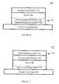
- the present inventionis power conditioning module 100 that may be disposed between device 200 (for example, an integrated circuit device such as a microprocessor) and printed circuit board 400 , as illustrated in FIG. 3, or between device 200 and thermal management module 300 , as illustrated in FIG. 4 .
- the location of power conditioning module 100 , relative to consuming device 200 and thermal management module 300may be selected according to power, thermal and space considerations of system 10 .
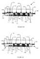
- the power conditioning module 100 of FIG. 2includes a semiconductor substrate 102 , interface vias 104 a- 104 h , interface pads 106 a- 106 p , power and ground vias 108 a and 108 b , power and ground pads 110 a and 110 b , and electrical circuitry 112 .
- the semiconductor substrate 102includes a first interface for mating or interfacing with device 200 and a second interface for mating or interfacing with a substrate or board 400 (for example, a system printed circuit board such as a mother or daughter board).
- the semiconductor substrate 102may be fabricated from a number of well known materials including, for example, silicon or germanium. In certain circumstances, it may be advantageous to use a material that is the same as, or has similar properties (for example, thermal expansion) to the material used for the substrate of device 200 . Such a configuration may provide for enhanced operating reliability since the similar thermal expansion properties of power conditioning module 100 and device 200 may minimize the potential for defects in the electrical connections between power conditioning module 100 and device 200 typically caused during operation because of differences in thermal expansion coefficients. Moreover, using the same material or materials permits the use of the same or similar fabrication techniques and facilities/equipment thereby potentially reducing manufacturing costs.
- the interface vias 104 a- 104 hprovide electrical connection for signals used by device 200 but not used by power conditioning module 100 in conditioning the power for device 200 .
- power conditioning module 100provides the electrical interconnects for other signals, such as the data and address signals, used by device 200 .
- interface vias 104 a- 104 hmay provide an electrical pathway, through power conditioning module 100 , between the microprocessor and, for example DRAM or SRAM memory devices.
- signals from other parts of system 10(for example, DRAM or SRAM memory devices) may travel or propagate by way of signal traces on printed circuit board 400 —through power conditioning module 100 —to device 200 by way of interface vias 104 - 104 h.
- the interface vias 104 a- 104 hmay be fabricated using conventional processing techniques. Where the number of signals that travel to and from device 200 is large, it may be preferable to employ highly anisotropic etching to form narrow pathways in substrate 102 and to deposit (for example, using CVD or LPCVD techniques) a highly conductive material such as gold, copper, aluminum, or highly doped polysilicon into the pathways to facilitate a highly conductive interconnection.
- highly anisotropic etchingto form narrow pathways in substrate 102 and to deposit (for example, using CVD or LPCVD techniques) a highly conductive material such as gold, copper, aluminum, or highly doped polysilicon into the pathways to facilitate a highly conductive interconnection.
- power conditioning module 100 of this embodimentmay further include interface pads 106 a- 106 p to facilitate greater conductivity between power conditioning module 100 and device 200 or board 400 .
- the interface pads 106 a- 106 pallow for greater tolerance in mating or interfacing power conditioning module 100 to board 400 and/or device 200 .
- the interface pads 106 a- 106 pmay be fabricated using conventional techniques from highly conductive material such as gold, copper or aluminum. In a preferred embodiment, the same material is used for both interface vias 104 a- 104 h and interface pads 106 a- 106 p .
- pads 106 a- 106 pmay be fabricated in the same or similar manner and materials as used in ball grid array (“BGA”) or chip scale package (“CSP”) devices.
- BGAball grid array
- CSPchip scale package
- power conditioning module 100may also include power and ground vias 108 a and 108 b to provide a supply voltage, supply current, reference voltages, and/or ground (supply) voltages to electrical circuitry 112 .
- the power and ground vias 108 a and 108 bmay be designed and fabricated in the same manner as interface vias 104 a- 104 h.
- power and ground vias 108 a and 108 bmay provide other voltages or currents that are necessary for electrical circuitry 112 to perform the functions described herein or any other desirable functions.
- the power conditioning module 100may also include power and ground pads 110 a and 110 b to enhance electrical conductivity between power conditioning module 100 and printed circuit board 400 .
- the power and ground pads 110 a and 110 blike interface pads 106 a- 106 p , permit for greater tolerance or mismatch in mating or interfacing power conditioning module 100 to board 400 .
- the power and ground pads 110 a and 110 bmay be designed and fabricated in the same manner as interface pads 106 a- 106 p.
- the power conditioning module 100also includes electrical circuitry 112 .
- the electrical circuitry 112delivers the conditioned power to device 200 .
- electrical circuitry 112provides appropriate conditioning of the voltage parameters (for example, supply voltage and ground) and current parameters (for example, supply, peak and typical operating currents) required by device 200 so that the voltage and current available to device 200 during, for example, normal operation, standby, start-up and/or shutdown, are within the ranges or tolerances required for proper and reliable operation.
- the electrical circuitry 112may include voltage regulators, bypass capacitors, DC-DC converters, and/or AC-DC converters arranged, configured, designed and interconnected using conventional techniques and designs (for example, conventional CMOS or BJT design and fabrication techniques). A brief overview of these elements is provided in the background of the invention and, for the sake of brevity, will not be repeated here.
- electrical circuitry 112such as voltage regulators, bypass capacitors, ferrite beads, DC-DC converters, and/or AC-DC converters near device 200 .
- electrical circuitry 112such as voltage regulators, bypass capacitors, ferrite beads, DC-DC converters, and/or AC-DC converters near device 200 .
- the horizontal and vertical space consumed by electrical circuitry 112is considerably reduced in relation to the conventional techniques and systems illustrated in FIG. 1 and contemplated in U.S. Pat. No. 6,285,550.
- locating power conditioning module 100 on or near thermal management module 300facilitates efficient capture and rejection of heat generated by electrical circuitry 112 in power conditioning module 100 .
- the electrical circuitry 112 illustrated in FIG. 2is disposed on the first interface of substrate 102 . This embodiment may facilitate interfacing with the electrical power and ground inputs of device 200 . However, it should be noted that electrical circuitry 112 may also be disposed on the second interface as illustrated in FIG. 4 . This configuration may, for example, enhance the thermal capture and rejection capabilities with respect to the electrical circuitry of power conditioning module 100 and enhance signal conductivity between device 200 and signal traces on printed circuit board 400 . In addition, the configuration illustrated in FIG. 4 may also suit the packaging requirements of device 200 and reduce the thermal exchange between power conditioning module 100 and consuming device 200 . The embodiment of FIG. 4 may also accommodate manufacturing constraints of electrical circuitry 112 of power conditioning module 100 .
- the electrical circuitry 112may also be disposed on both the first and second interfaces.
- a layout having electrical circuitry 112 disposed on the first and second interfacesmay provide many of the advantages of both FIGS. 3 and 4.
- power conditioning module 100While it is contemplated that the power conditioning requirements of device 200 are satisfied by power conditioning module 100 , it should be noted that additional discrete electrical power conditioning elements (for example, by-pass capacitors (not shown) to provide filtering, in addition to that performed by power conditioning module 100 , also may be employed and disposed in manners similar to that of conventional systems. Under this circumstance, power conditioning module 100 does not perform all power conditioning functions of system 10 . Rather, power conditioning module 100 performs power conditioning in conjunction with discrete electrical power conditioning elements. These discrete electrical power conditioning elements may perform initial and/or supplemental conditioning of the voltage and current. For example, a system may include a primary power supply (having discrete components) to provide initial power conditioning of an externally supplied power.
- a primary power supplyhaving discrete components
- the power conditioning module 100provides localized power conditioning of the power for device 200 .
- the primary power supplymay provide initial power conditioning for a plurality of devices in the system, including device 200 (See, for example, FIG. 24 ).
- the additional discrete electrical power conditioning elementsmay increase the footprint of the power conditioning of the overall system.
- the reference voltages and currents used by electrical circuitry 112may be provided or routed to the particular elements (for example, voltage regulators) of electrical circuitry 112 in many ways.
- the voltage and currentmay be provided to electrical circuitry 112 using power and ground conduits 114 a and 114 b that are embedded within semiconductor substrate 102 .
- the power and ground conduits 114 a and 114 bextend from power and ground vias 108 a and 108 b and connect to electrical circuitry 112 as dictated by the specific power conditioning circuit design implemented.
- power and ground vias 108 a and 108 bneed not extend the entire length of semiconductor substrate 102 (as illustrated in FIG.
- power and ground conduits 114 a and 114 bconnect well within substrate 102 .
- the power and ground conduits 114 a and 114 bmay be fabricated using conductive materials (for example, gold, copper, aluminum or a highly doped polysilicon) and deposited using conventional semiconductor processing or fabrication techniques (for example, conventional photolithography, etching and deposition processes).
- power and ground conduits 114 a and 114 bmay also be formed more towards the interface of semiconductor substrate 102 (but still in substrate 102 ).
- power and ground vias 108 and 108 bmay extend the entire or nearly the entire length of semiconductor substrate 102 since power and ground conduits 114 a and 114 b connect to electrical circuitry 112 nearer the surface of the interface of substrate 102 .
- the power and ground conduits 114 a and 114 b of FIG. 6extend from power and ground vias 108 a and 108 b (not illustrated in FIG. 6) and connect to electrical circuitry 112 which is also fabricated near the interface of substrate 102 .
- the power and ground conduits 114 a and 114 bmay be fabricated using conventional processing or fabrication techniques from conductive materials (for example, gold, copper, aluminum or a highly doped polysilicon).
- FIGS. 4 and 7Another alternative for supplying power and ground to electrical circuitry 112 is illustrated in FIGS. 4 and 7.
- power and groundare provided to electrical circuitry 112 using conventional wire bonding techniques that employ conventional wires 120 and bond pads 122 as illustrated in FIG. 4 .
- Those skilled in the artwill appreciate that there are many techniques for providing power and ground connections from board 400 (or a power supply, not shown) to electrical circuitry 112 . All techniques for providing power and ground connections to and from electrical circuitry 112 , whether now known or later developed, are intended to be within the scope of the present invention.
- electrical circuitry 112conditions the power, in a conventional manner, and delivers the required power to device 200 .
- the electrical circuitry 112(for example, voltage regulators, bypass capacitors, DC-DC converters, and/or AC-DC converters) may be arranged and interconnected using conventional techniques and designs (for example, conventional CMOS and/or BJT circuit designs to accomplish the necessary power conditioning functions) to provide device 200 with the appropriate voltage and current during all aspects of operation as well as during start-up, standby and shutdown.
- the output power and/or ground of power conditioning module 100may be provided or routed to device 200 using techniques similar to those used in providing electrical circuit 112 with the “unconditioned” power and ground from board 400 (or power supply, not shown).
- electrical circuitry 112supplies the conditioned power and/or ground to device 200 using output power conduit 116 a , output ground conduit 116 b , output power via 118 a , and output ground via 118 b .
- Signal tracesmay then provide electrical connection between output power and ground conduits 116 a and 116 b to power and ground inputs of device 200 .
- output power and output ground conduits 116 a and 116 bmay be directly routed to the specified pads on the interface of substrate 102 that match or correspond to the power and ground inputs of device 200 .
- vias 118 a and 118 bmay be eliminated because output power and ground conduits 116 a and 116 b are routed to the appropriate power and ground inputs of device 200 without an intermediate connection.
- the output power and/or ground of power conditioning module 100may be routed to device 200 in the manner illustrated in FIG. 6 .
- output power and ground conduits 116 a , 116 b and 116 care formed in substrate 102 using conventional fabrication techniques and routed to a predetermined pads 106 x , 106 y and 106 z which corresponds to power or ground inputs of device 200 .
- the power and ground conduits 116 a and 116 bmay be fabricated from electrically conductive materials (for example, gold, copper, aluminum or a highly doped polysilicon).
- output power and ground of power conditioning module 100may also be routed to device 200 in the manner illustrated in FIG. 7 .
- output power and groundare provided to device 200 using conventional wire bonding techniques.
- conventional wires 120and bond pads, not shown interconnect the output of power conditioning module 100 to the appropriate inputs of device 200 .
- power conditioning module 100may be fabricated using a 2 -stage process, in which vias 104 and 108 (and other elements, for example power and ground conduits 114 and 116 ) are formed first and electrical circuitry 112 fabricated using conventional CMOS or BJT processing is formed second. Indeed, it should be understood that any techniques for fabricating (as well as the materials used therein) power conditioning module 100 now known or later developed are intended to be within the scope of the present invention.
- the present inventionis advantageously suitable for use in space-constrained environments.
- locating the power conditioning elements in essentially the same basic footprint as the integrated circuit devicepermits the space around the integrated circuit device to be used for other purposes.
- external static or dynamic memorymay be located closer to the microprocessor thereby reducing the flight times of signals communicating with the memory. This may result in faster system operation.
- the power conditioning module 100may be located between device 200 and board 400 as illustrated in FIG. 3 .
- a configuration of power conditioning module 100 as illustrated in FIG. 2is more suitable because the vias, among other things, facilitate electrical connection for those signals used by device 200 (but not by power conditioning module 100 ), for example data and address signals for DRAM or SRAM memory devices.
- power conditioning module 100may be located between device 200 and thermal management module 300 as illustrated in FIGS. 4 and 7.
- active electrical layerfor example, electrical circuitry 112
- thermal management module 300may be a fan that causes air to travel over the elements of system 10 and thereby remove the heat generated by module 100 and device 200 .
- thermal management module 300may be placed in an area having sufficient volume for a fan, without interfering with other system needs for placement of peripherals, such as memory or data storage, in close proximity to device 200 .
- thermal management module 300it may be advantageous to implement a more compact thermal management module 300 than a conventional fin-array heat sink as illustrated in FIG. 3 .
- a thermal capture elementhaving a micro channel structure to capture and remove heat generated by device 200 and/or electrical circuitry 112 . The heat energy may then be rejected by a heat rejection element that is either local or remote relative to device 200 .
- any techniques known or later developed for heat capture and rejection apparatus or sub-system, including any of those described herein,are intended to be within the scope of the present invention.
- thermal management module 300may be unnecessary altogether.
- “cool chips”such as the “Crusoe” processor from Transmeta Inc., feature low thermal profiles.
- system 10may be implemented in a space-constrained environment (for example, portable or handheld devices), due to its small footprint, and be unconcerned with thermal capabilities and space considerations of thermal management module 300 .
- the present inventionis an integrated power and thermal management module that incorporates the functions of the power conditioning element (i.e., power conditioning) and the thermal management element (i.e., heat capture, removal and/or rejection) into a single structure.
- the modules for power conditioning and heat capture, removal and rejectionwere separate structures that were stacked, with device 200 , in various configurations to form a 3-layer structure.
- the power conditioning element and the thermal management elementare incorporated into a single structure.
- additional advantagesmay be realized including, for example, a significant reduction in the total volume occupied and direct physical contact may be achieved between the consuming device, the power conditioning module and the thermal management module—thereby facilitating enhanced thermal capture and rejection for the power conditioning structure and/or the consuming device.
- This aspect of the inventionalso provides unique packaging configurations of the combined power conditioning and thermal management module—consuming device structure. It should be noted that since the consuming device and the power conditioning module capitalize on the thermal management capabilities of the integrated power conditioning and thermal management module, additional heat capture and rejection elements may be unnecessary. This may be important because, in some instances, the operational temperatures of the power conditioning module may approach that of device 200 .
- thermal management elementfacilitates implementation of the integrated power conditioning and thermal management module in highly space-constrained environments.
- heat capture and heat rejection aspects of the thermal management element of module 1000are separated such that the thermal capture functions are integrated into a single structure with the power conditioning functions, that single structure (i.e., power conditioning and thermal management module 1000 as in FIG. 8) may be implemented within the packaging of an integrated circuit device. (See, for example, FIG. 11 ).
- the heat rejection functionsmay be accomplished using a heat sink disposed on a surface of the device/package or located distant from the device/package.
- power conditioning and thermal management module 1000includes power conditioning element 1100 .
- the power conditioning element 1100may be substantially similar to power conditioning module 100 of FIGS. 2-7 and may include, for example, vias, pads, and electrical circuitry as described above. For the sake of brevity, the details and functions of power conditioning element 1100 will not be repeated here.
- the power conditioning and thermal management module 1000also includes thermal management element 1200 .
- Thermal management element 1200captures and removes the heat generated by device 200 and/or power conditioning element 1100 so that the temperature of device 200 and/or power conditioning element 1100 does not exceed a given temperature.
- the thermal management element 1200may also reject the heat.
- thermal management element 1200captures the heat generated by device 200 and power conditioning element 1100 and removes that heat so that it may be dispersed in the surrounding environment by convection or a heat rejection element (for example, a conventional heat sink).
- Power conditioning and thermal management module 1000may include substrate 102 a , in which a substantial portion of power conditioning element 1100 is formed, and substrate 102 b , in which a portion of thermal management element 1200 is formed.
- the two substratesmay be bonded by, for example, anodic or fusion bonding, or eutectic bonding, or adhesive bonding for glass and semiconductor structures. Employing metal structures permits bonding by welding, soldering, eutectic bonding, or adhesives.
- the combined substrates 102 a and 102 bform power conditioning and thermal management module 1000 .
- interface vias that provide electrical connection between signal traces on printed circuit board 400 and inputs/outputs of device 200may be fabricated in two steps.
- a separate set of interface viasare formed in each of the substrates of power conditioning element 1100 and thermal management element 1200 . Thereafter, when the two substrates are bonded, a corresponding one of the interface vias in substrate 102 a mates with a corresponding one of the interface vias in substrate 102 b to form the interface via for module 1000 .
- intermediate interface padsmay be disposed on each of the mating interfaces of substrate 102 a and 102 b .
- the pads on each mating interfaceafter the two substrates are bonded, contact a corresponding pad on the other mating interface.
- This configurationallows for greater tolerance when mating or interfacing power conditioning element 1100 and thermal management element 1200 and, as such, may enhance the electrical continuity between the exposed interfaces of power conditioning and thermal management module 1000 when the bonded substrates are not perfectly aligned.
- thermal management element 1200includes a micro channel heat exchanger 1210 having a plurality of micro channels 1220 .
- the micro channel heat exchanger 1210also includes pump 1230 , fluid inlet 1240 , fluid outlet 1250 , and tubing 1260 to provide a fluid to micro channels 1220 .
- micro heat exchanger 1210may be, for example, a micro fabricated semiconductor substrate, machined metal substrate, or machined glass substrate.
- FIGS. 10A and 10Billustrate a top and cross sectional view, respectively, of an exemplary micro channel structure 1220 .
- the substrate of thermal management element 1200includes a pattern of micro channels 1220 - 1 and 1220 - 2 etched into an interface.
- the micro channels 1220 - 1 and 1220 - 2may be arranged on the interface of thermal management element 1200 according to the needs for heat removal from particular regions of power conditioning element 1100 .
- micro channel structure 1220may be increased in regions that correspond to anticipated or measured sources of excessive heat, or the routing of micro channels 1220 - 1 and 1220 - 2 may be designed to reduce and/or minimize temperature gradients from the inlet to the outlet of micro heat exchanger 1210 .
- the widths, depths, and shapes of micro channels 1220 - 1 and 1220 - 2may also be designed and fabricated to improve device temperature uniformity or address a hot spot on device 200 and/or power conditioning element 1100 .
- the shape and arrangement of micro channel structure 1220may be designed or determined through the assistance of thermal modeling tools described in a U.S. Patent Application entitled “Electroosmotic Microchannel Cooling System”, filed by Kenny, et al. on Jan. 19, 2002.
- Many different types of arrangements, layouts and configurations of micro heat exchanger 1210 and micro channels 1220 - 1 and 1220 - 2are described and illustrated in the U.S. Patent Application filed by Kenny et al. on Jan. 19, 2002.
- the U.S. Patent Application filed by Kenny et al. on Jan. 19, 2002has been assigned Application Ser. No. 10,053,859.
- the Kenny et al. U.S. Patent Applicationwill be referred to hereinafter as “the Kenny et al. Application”).
- the Kenny et al. Applicationis hereby incorporated, in its entirety, by reference herein.
- micro channels 1220may also extend into the interface of power conditioning element 1100 as well.
- micro channel structure 1220may be formed on both the first and second mating interfaces of thermal management module 1100 .
- micro heat exchanger 1210may more efficiently capture and remove heat from both device 200 and power conditioning element 1200 due, in part, to more intimate physical contact between the heat exchanger 1210 and both device 200 and power conditioning element 1200 .
- the micro heat exchanger 1210may also include more than one fluid path, as illustrated in FIG. 10A, by micro channels 1220 - 1 and 1220 - 2 . These independent paths may be connected to different pumps 1230 and/or different heat rejection elements 1410 , according to the particular needs and/or designs of the application. As mentioned above, many different types of arrangements, layouts and configurations of micro heat exchanger 1210 and micro channels 1220 - 1 and 1220 - 2 , including the multiple independent micro channel configuration, are described and illustrated in the Kenny et al. Application, which are again hereby incorporated by reference.
- the pump 1230may be any type of pumping device that provides the flow and pressure necessary to capture the heat generated in device 200 and/or power conditioning element 1100 .
- pumpmay be an electro-osmotic type pumping device like that described and illustrated in the Kenny et al. Application.
- the electro-osmotic type pumping deviceis not discussed in detail here, rather the corresponding discussion in the Kenny et al. Application is incorporated herein by reference.
- the power conditioning and thermal management module 1000 of FIGS. 8 and 9facilitates efficient packaging of power conditioning element 1100 in close proximity to device 200 , and provides an additional advantage that the heat generated by power conditioning element 1100 and/or device 200 is captured within, and removed by thermal management element 1200 . Further, by positioning the power conditioning and heat capture elements within a single module beneath device 200 , a surface (for example, the top or upper surface) of device 200 is available for other modes of access, such as optical or RF telecommunications, and/or for placement of memory devices. This positioning also permits that surface of device 200 to be used for other functions, including, for example, additional thermal management elements such as a heat sink as illustrated in FIG. 3 or a second thermal management element as illustrated in FIGS. 17A and 17B.
- additional thermal management elementssuch as a heat sink as illustrated in FIG. 3 or a second thermal management element as illustrated in FIGS. 17A and 17B.
- power conditioning and thermal management module 1000 of FIGS. 8 and 9facilitates efficient packaging as a discrete device.
- module 1000may be incorporated into a typical electronic package 1300 , having pins 1310 , that is modified to accommodate fluid required for thermal management element 1200 .
- the device 200 illustrated in the embodiment of FIG. 11may employ a conventional face-down, ball-bond mounting configuration to an electrical interconnect array.
- the device 200may be mounted to power and thermal management module 1000 in a manner similar to that described above with respect to the embodiment illustrated in FIGS. 2-7.
- Employing a face-down, ball-bond mounting configuration for device 200provides several additional advantages, including, for example, providing intimate contact between device 200 with the heat capture capabilities of thermal management element 1200 (and the fluid-filled micro channels 1220 ); and permitting back-surface access to device 200 for other purposes, as described above.
- the device 200 illustrated in the embodiment of FIG. 12Amay employ a conventional face-up, wire bond mounting configuration where wire bonds provide connection from device 200 to package 1300 .
- the interconnect viasare unnecessary since conventional wire bonding techniques provide the electrical connection to device 200 .
- this embodimentprovides several significant advantages, including, for example, incorporation of power conditioning and heat capture elements into package 1300 thereby providing close proximity of power conditioning element 1100 to device 200 .
- this embodimentprovides an advantage of providing intimate contact between device 200 , power conditioning element 1100 and thermal management element 1200 so that energy (in the form of heat) generated by device 200 and/or power conditioning element 1100 may be efficiently captured (by the fluid in micro channels 1220 ) are removed from package 1300 .
- 12Ais that the operating surface of device 200 is optically accessible, which would be suitable for use by another device, for example, an electro-optic device, such as a modulator, a display device, an optical imaging device, such as a CCD, and/or an optical switch.
- an electro-optic devicesuch as a modulator
- a display devicesuch as a liquid crystal display
- an optical imaging devicesuch as a CCD
- an optical switchsuch as a CCD, and/or an optical switch.
- a lid 1320may be attached to package 1300 thereby providing a hermetically-sealed environment with integrated power conditioning and thermal management capabilities of module 1000 in intimate contact with device 200 .
- the lid 1320may be opaque, as would be appropriate for an opto-electronic device, or lid 1320 may be transparent in the infrared or visible spectrums, as would be appropriate for a display device, or an imaging device. Integration of the power and thermal management functions within this package may allow optimal operation of thermally-sensitive devices, such as imaging arrays.
- the working fluidis provided to micro heat exchanger 1210 from beneath power conditioning and thermal management module 1000 using channels or tubing 1260 that are embedded or formed in the substrate. Press fits, solder and/or adhesives may secure the channels or embedded tubing 1260 directly to fluid inlet (not shown) and fluid outlet (not shown) of micro heat exchanger 1210 .
- the configuration of FIG. 13may facilitate implementation of module 1000 in a chip pick-place assembly process.
- channel or tubing 1260there are many possible techniques of attaching channel or tubing 1260 to module 1000 , including, for example, formation of openings in module 1000 to permit tubing segments and/or other couplings to be inserted into module 1000 and bonded into place. These bonds may be press-fits, or utilize solder or adhesives. Alternatively, it is possible to form openings in module 1000 on the top or bottom surfaces, and to bond a fitting to one or both of these surfaces over the opening(s) with a port for connecting the tube. Indeed, all techniques, now known or later developed, for securing embedded channels or tubing 1260 to the fluid inlet and outlet of micro heat exchanger 1210 are intended to be within the scope of the present invention.
- the embedded channel configuration of FIG. 13also may be employed in those circumstances where the consuming device and power conditioning and thermal management module 1000 are packaged and that package is affixed to a substrate.
- the working fluidmay be provided to the micro heat exchanger of power conditioning and thermal management module using channels or tubing that are embedded or formed in the substrate to which the consuming device is affixed.
- the fittingsmay be employed to secure the channels (or embedded tubing) directly to the fluid inlet and outlet of the micro heat exchanger or the fluid inlet and outlet of the package.
- tubing or channels embedded or formed in the packagemay provide the interconnection between the channels (or tubing) in the substrate and the fluid inlet and outlet of the micro heat exchanger.
- the power and thermal management module 1000may also include circuits or devices that provide information regarding the operating parameters of module 1000 for more efficient and responsive cooling and power conditioning.
- power and thermal management module 1000 of this embodimentadditionally includes sensors 1270 (for example, temperature, pressure and flow sensors) and controller 1280 .
- the sensors 1270provide information that is representative of the operating conditions of device 200 and module 1000 (for example, operating temperature).
- the signals from sensors 1270may be routed to controller 1280 to provide a closed-loop control of the functionality of power and thermal management module 1000 .
- controller 1280may use information provided by the temperature sensor to modify or adjust the operation of thermal management element 1200 , power conditioning element 1100 and/or device 200 .
- power conditioning and thermal management module 1000is being operated in a thermal control mode, in which the temperature variations measured by one or more temperature sensors that are distributed throughout module 1000 are provided as feedback signals to controller 1280 .
- the controller 1280may use the information provided by sensors 1270 to determine, for example, the average temperature of module 1000 and/or device 200 and spatial variations in temperature with respect to module 100 and/or device 200 .
- controller 1280may adjust the fluid flow rate through micro channels 1220 of micro channel heat exchanger 1210 .
- the controller 1280may adjust the rate of fluid flow in micro channels 1220 by controlling the operation of pump 1230 or by adjusting the distribution of the fluid through the different channel manifolds of micro channel heat exchanger 1210 .
- controller 1280after determining a temperature sensitive condition, may alert device 200 that it may exceed (or has exceeded) its normal operating temperature. In response device 200 may initiate a low power mode in order to lower its operating temperature and power consumption. Consuming less power will result in less heat generation by device 200 as well as power conditioning element 1100 . The device 200 , in response to information regarding its operating temperature, may enter a system shut down process as a protective measure. Other actions in response to changes in temperature are described in the Kenny et al. Application, which are hereby incorporated by reference herein.
- sensors 1270for example, temperature, pressure, and/or flow sensors
- the placement or location of sensors 1270may be based on many factors. For example, there may be advantages to place the temperature sensors laterally with respect to the micro channels 1220 and the anticipated or measured sources of heat of electrically circuitry 112 and/or device 200 . Moreover, there may be advantages to placement of temperature sensors at different depths (vertical locations) in substrates 102 a and 102 b .
- FIGS. 10A, 10 B, 14 and 15illustrate sensors 1270 disposed in various locations in power conditioning element 1100 and thermal management element 1200 .
- the sensors 1270provide information indicative of the operating conditions (for example, temperature) of a specific region(s) of device 200 and module 1000 to controller 1280 .
- power and thermal management module 1000may include more than one pumping mechanism. Additional pumping mechanisms may be implemented to provide more immediate and direct control of fluid flow in particular regions of module 1000 . This may be important in those situations where there are expected hotspots in device 200 and/or power conditioning elements 1100 .
- more than one pumpmay be implement in configuration where micro heat exchanger 1210 includes separate and independent micro channels 1220 paths, as illustrated in FIG. 10 A. Additional embodiments employing more than one pumping mechanism are described in detail in the Kenny et al. Application, which is hereby incorporated by reference herein.
- power and thermal management module 1000 of FIG. 15provides, among other things, power conditioning functions for device 200 , and cooling functions for maintaining device 200 and/or power conditioning elements 1100 within acceptable temperature ranges.
- the controller 1280in conjunction with sensors 1270 , permits analysis and detection of changes in the operating parameters of device 200 and power and thermal management module 1000 . Such changes may result from changes in the power usage by device 200 .
- thermal management element 1200may adjust the cooling capability (by, for example, control signals to the fluid pump(s) to increase the rate of fluid flow) in order to maintain the temperature of device 200 within acceptable temperature ranges.
- the power and thermal management module 1000may also include current sensors to detect the current consumption of device 200 .
- current sensor 1290may be embedded in semiconductor substrate 102 a to provide information which is representative of the current consumption of device 200 and/or electrical circuitry 112 to controller 1280 .
- the controller 1280may use the detected current consumption to modify the operation of thermal management element 1200 .
- controller 1280may adjust the fluid cooling capability of thermal management element 1200 by increasing or decreasing the fluid flow of pump 1230 .
- controller 1280may anticipate a change in temperature of device 200 and/or power conditioning element 1100 .
- current sensor(s) 1290may also detect the current passing through electrical circuitry 112 of power conditioning element 1100 (for example, the voltage regulation devices).
- the current passing through electrical circuitry 112may be representative of the current and/or power consumption or demand of device 200 .
- the controller 1280may use the information from sensor(s) 1290 to determine appropriate actions to be taken in anticipation of an increase or decrease in temperature as a result of a change in the current consumption of device 200 and/or power conditioning element 1100 .
- the controllermay also use that information to determine anticipated heat capture and rejection requirements as a result of a change in the current consumption.
- micro channel heat exchanger 1210may be modified by altering the rate of flow of the working fluid in micro channels 1220 (for example, by adjusting the output flow rate of pump 1230 ). Further, controller 1280 may also adjust the heat rejection capabilities after the heat is captured and removed from device 200 and module 1000 . Other techniques for changing the heat capture and removal capabilities of micro channel heat exchanger 1210 are described in the Kenny et al. Application, which are hereby incorporated by reference.
- sensor(s) 1290are integrated with the voltage regulators in power conditioning element 1100 . It should be noted that controller 1280 may also determine the power requirements and/or consumption of device 200 indirectly from the power consumed during operation of device 200 . The controller 1280 may then use that information to determine or implement an appropriate course of action, for example, by adjusting the heat capture and removal capabilities of micro channel heat exchanger 1210 or heat rejection capabilities of the system, as discussed above.
- controller 1280may be implemented within device 200 .
- device 200determines its power consumption using, for example, information from sensors 1270 (for example, temperature, pressure, flow) and/or current sensor 1290 , or information regarding clock rate, electrical activity in subsystems such as floating-point processors, image processing circuits, and analog current output circuits.
- device 200may adjust the power delivery capabilities of power conditioning element 1100 .
- the device 200may also adjust the heat capture, removal and/or rejection capabilities of thermal management element 1200 .
- Employing device 200 to perform some or all of the functions/operations previously performed by controller 1280facilitates use of information typically available to devices (for example, clock rate), as well as use of computational resources that may already exist in device 200 .
- the device 200 and/or controller 1280may implement sophisticated control algorithms that allow device 200 and/or controller 1280 to determine an appropriate action or response of thermal management element 1200 so that the temperature of device 200 and/or power conditioning element 1100 is maintained within a narrow range. That information may be used to develop a heat capture/rejection operational procedure that achieves an optimal balance between temperature variations of device 200 and operational costs of power and thermal management module 1000 . Such operational costs may be power consumption by device 200 , computational complexity, and/or operation within preferred flow and thermal ranges.
- device 200 and/or controller 1280may use information indicative of the operation of device 200 to predict variations in the spatial distribution of the power dissipation within device 200 .
- the power consumption of the floating point processorwhich takes up a small fraction of the processor's surface, may temporarily exceed the power consumption of the remainder of the microprocessor.
- the temperature of this subsystem of the microprocessormay rise rapidly to temperatures that exceed the recommended operational temperatures.
- closed-loop power conditioning and thermal management system 2000includes power conditioning and thermal management module 1000 , as discussed above, in conjunction with thermal capture and rejection module 1400 .
- power conditioning and thermal management module 1000is disposed on printed circuit board 400
- device 200is disposed on power conditioning and thermal management module 1000
- thermal capture and rejection module 1400is disposed on device 200 .
- power conditioning element 1100 of power conditioning and thermal management module 1000is disposed in close proximity to device 200 thereby providing the power conditioning advantages described above.
- micro channel heat exchanger 1210is disposed in close proximity to power conditioning element 1100 thereby facilitating enhanced heat capture, removal and rejection in order to maintain the temperature of power conditioning element 1100 within an acceptable range.
- the heat captured by thermal management element 1200is provided (via fluid flow) to heat rejection element 1410 of thermal capture and rejection module 1400 .
- the thermal capture and rejection module 1400rejects the heat provided by thermal management element 1200 using heat rejection element 1410 , which is illustrated as a heat sink having fins, and thermal capture element 1420 .
- the heat rejection element 1410may employ many different types of heat rejection techniques, including a design having a fluid flow path or paths throughout the high-surface-area structures (such as fluid channels in the fins) as described and illustrated in the Kenny et al. Application. All of the thermal capture, removal and rejection techniques described and illustrated the Kenny et al. Application are hereby incorporated by reference.
- Thermal capture element 1420includes a micro channel heat exchanger 1430 which facilitates localized heat capture, removal and, in conjunction with heat rejection element 1410 , rejection of heat generated primarily by device 200 .
- the micro channel heat exchanger 1430includes a plurality of micro channels 1440 (which, in operation contain a fluid) for efficient heat capture from device 200 .
- the micro channel heat exchanger 1430including micro channels 1440 , may be fabricated in the same manner and using the same materials as micro heat exchanger 1210 and micro channels 1220 .
- the micro channel heat exchanger 1430may be, for example, arranged at the interface of thermal capture element 1420 in accordance with the needs for heat removal from particular regions of device 200 .
- the density of micro channels 1440may be increased in regions that correspond to anticipated or measured sources of excessive heat.
- the routing of micro channels 1440may be designed to reduce and/or minimize temperature gradients from the inlet to the outlet of micro heat exchanger 1420 .
- the widths, depths, and shapes of micro channels 1440may also be designed and fabricated to improve device temperature uniformity across device 200 . Indeed, the shape and layout of micro channels 1440 may be designed through the assistance of thermal modeling tools described in the Kenny et al. Application. Many different types of arrangement, layouts, configurations and design techniques of micro heat exchanger 1420 and micro channels 1440 are described and illustrated in the Kenny et al. Application, which are hereby incorporated, in total, by reference.
- micro channels of micro heat exchanger 1420may be disposed on both interfaces of thermal capture element 1420 to enhance the thermal capture, removal and/or rejection from the heat generating device(s).
- micro channel heat exchanger 1430may be configured as an array of micro channel pillars. In this regard, an array of vertical channels are interconnected laterally on an interface (or on both interfaces) of thermal capture element 1420 . This configuration may further enhance the thermal capture, removal and/or rejection of heat energy generated by device 200 and/or power conditioning and thermal management module 1000 .
- pump 1230is disposed between thermal capture and rejection module 1400 and heat rejection element 1410 .
- the pump 1230may be an electro-osmotic pumping device as described in detail in the Kenny et al. Application. Many different types of configurations and designs of pump 1230 are acceptable including those described and illustrated in the Kenny et al. Application, which are hereby incorporated by reference.
- system 2000may employ multiple pumps and/or independent fluid cooling loops to allow for independent control of the heat capture capabilities at different locations within module 1000 . This feature is also discussed in detail in the Kenny et al. Application, and is also hereby incorporated by reference.
- heat rejection element 1410may be located remotely from the other elements of system 2000 .
- Such a configurationfacilitates use of system 2000 in a space-constrained environment yet provides sufficient power conditioning and thermal management in a small footprint.
- tubing 1260provides a fluid path for fluid heated by device 200 and power conditioning element 1210 to heat rejection element 1410 .
- the remotely located heat rejection element 1410may be placed in an area having sufficient volume for a fin array (and possibly with a fan), without interfering with other system needs for placement of peripheral system elements such as memory or data storage in proximity to device 200 .
- heat rejection functionalitymay be unnecessary altogether.
- the power conditioning and thermal management module 1000 of FIGS. 8-17Billustrate the power conditioning element disposed on the thermal management element.
- thermal management element 1100is disposed on power conditioning element 1200 .
- thermal management element 1200may more efficiently capture and remove heat generated by device 200 because of the proximity of the micro channels to device 200 .
- the capture and removal of heat from electrical circuitry 112 of power conditioning element 1100may remain relatively unchanged.
- thermal management element 1200may more efficiently capture and remove heat generated by both device 200 and power conditioning element 1100 .
- a heat rejection elementfor example, a heat sink, not shown
- micro channels 1220may also extend into the interface of power conditioning element 1100 .
- micro channel structure 1220may be formed on both the first and second mating interfaces of thermal management module 1100 .
- micro heat exchanger 1210may even more efficiently capture and remove heat from both device 200 and power conditioning element 1200 due, in part, to more intimate physical contact of the heat exchanger 1210 with both device 200 and power conditioning element 1200 .
- the electrical circuitry of the power conditioning elementremains in close proximity with the device thereby providing all of the power conditioning advantages described above.
- the power conditioning and thermal management module 1000 of FIG. 18may be fabricated and implemented in the same manner as the power conditioning and thermal management module 1000 illustrated in FIG. 8 .
- power conditioning and thermal management module 1000 of FIG. 18may include all of the features, additions, attributes, and embodiments of power conditioning and thermal management module 1000 of FIGS. 8-17B.
- power conditioning and thermal management module 1000 of FIG. 18may include, for example, a controller, parameter sensor(s) (for example, temperature, pressure and flow) to measure or detect the operating conditions of device 200 and/or power conditioning element 1200 , and current sensor(s) to monitor the current consumed by device 200 and/or power conditioning element 1200 .
- the power conditioning and thermal management module 1000 of FIG. 18may also include multiple independent micro channels to allow independent thermal capture and removal of designated areas of device 200 and/or power conditioning element 1200 .
- power conditioning and thermal management module 1000 of FIG. 18may be implemented in the packaging configurations of FIGS. 11, 12 A and 12 B in essentially the same manner as the embodiment of FIG. 8 . Indeed, all of the features and attributes of power conditioning and thermal management module 1000 illustrated in FIGS. 8-17B, and described above, are equally applicable to the power conditioning and thermal management module of FIG. 18 . For the sake of conciseness, the details of the features and attributes of the embodiments will not be repeated here.
- power conditioning and thermal management module 1000may route the signals to and from device 200 using all of the same techniques as described above with respect to FIGS. 2-17B. Moreover, power and ground may be routed to and from electrical circuitry 112 and device 200 using those same techniques.
- the embodiment of FIG. 18may employ the routing technique described in the embodiment of FIG. 6 wherein the output power and ground conduits are formed in substrate using conventional fabrication techniques and are routed to predetermined pads which corresponds to power or ground inputs of device 200 . Under this circumstance, output power and ground conduits are routed directly to the power and ground inputs of device 200 .
- the power conditioning element and the micro channel structure of the thermal management elementare fabricated in the same substrate—rather than two substrates 102 a and 102 b , as described above and illustrated in FIGS. 8 and 18 .
- micro channel structure 1210 and power conditioning element 1100are fabricated in the same substrate.
- the assembly costsmay be reduced because the thermal management element and the power conditioning element need not be assembled from two separate substrates before interfacing with the consuming device and another substrate (for example, a printed circuit board).
- the capture and removal of heat from the consuming devicemay be enhanced, relative to the embodiment of FIG. 9, because of the proximity of the micro channels to the heat generating circuitry disposed on the consuming device.
- the capture and removal of heat from electrical circuitry 112 of power conditioning element 1100may be sufficient and, as such, this embodiment may not require additional heat removal, capture and rejection capabilities from, for example a heat sink and/or fan.
- micro channel structure 1210 of thermal management element 1200may be fabricated using conventional micro channel fabrication techniques and/or those techniques described and illustrated in the Kenny et al. Application, which are hereby incorporated by reference. Thereafter, electrical circuitry 112 of power conditioning element 1100 may be fabricated using conventional CMOS or BJT design and fabrication techniques. In this embodiment, the interface, power and ground vias may be fabricated before or after the formation of the micro channel structure. The pads (if any) that connect to the vias may be fabricated after fabrication of electrical circuitry 112 and micro channels 1220 .
- power conditioning and thermal management module 1000 of FIG. 19Amay include, for example, a controller, parameter sensor(s) (for example, temperature, pressure and flow), and current sensor(s).
- the power conditioning and thermal management module 1000 of FIG. 19Amay also include pump(s) and multiple independent micro channels to allow independent thermal capture and removal of designated areas of device 200 and/or power conditioning element 1200 .
- power conditioning and thermal management module 1000 of FIG. 18Amay be implemented in the packaging configurations of FIGS. 11, 12 A and 12 B. Indeed, all of the features and attributes of the power conditioning and thermal management module 1000 illustrated in FIGS. 8-18, and described above, are equally applicable to the power conditioning and thermal management module of FIG. 19 A.
- power conditioning and thermal management module 1000may route the signals to and from device 200 using any of the signal routing techniques described above.
- Power and groundmay be routed to and from electrical circuitry 112 and device 200 using those same techniques, including the techniques illustrated in FIG. 6 and described above.
- electrical circuitry 112 of power conditioning element 1100may be subjected to micro channel processing without damage, electrical circuitry 112 may be fabricated before fabrication of the micro channel structure.
- the interface, power and ground viasmay be fabricated before or after the formation of the micro channel structure.
- the pads (if any) that connect to the viasmay be fabricated after the other elements of power conditioning and thermal management module 1000 .
- the power conditioning element and micro channel structure of thermal management element 1200are fabricated in one substrate.
- the entire micro channel structure, or a portion of that structuremay be fabricated on the backside of device 200 .
- micro channels 1220 of micro channel structure 1210may be fabricated entirely in device 200 (FIG. 19B) or partially in device 200 and power conditioning element 1100 (FIG. 19 C).
- Another aspect of the present inventionis the use of the module and/or elements described herein (for example, power conditioning module 100 , power conditioning and thermal management module 1000 , thermal capture and rejection module 1400 , heat rejection element 1410 and thermal capture element 1420 ) as building blocks in designing a system having local power conditioning functionality as well as heat capture, removal and/or rejection capabilities.
- device 200is disposed on printed circuit board 400
- thermal capture element 1420is disposed on device 200 to facilitate capture of localized heat generated by device 200 .
- the power conditioning and thermal management module 1000is disposed on thermal capture element 1420 .
- heat rejection element 1410(for example, a heat sink having fins) may be disposed on thermal management element 1200 to permit enhanced rejection of the heat captured by thermal management element 1200 (generated primarily by power conditioning element 1100 ) and thermal capture element 1420 (generated primarily by device 200 ).
- power conditioning element 1100is in close proximity to device 200 .
- Power and ground connections to and from power conditioning element 1100may be accomplished using a wire bond configuration described herein. (See, for example, FIGS. 4 and 7 ).
- the pumpmay be an electro-osmotic type pump(s) located in thermal management module 1200 and/or thermal capture element 1420 . Moreover, the pump need not be located in thermal management module 1200 or thermal capture element 1420 but rather may be a “stand alone”) device. As suggested above, the pump may include a plurality of pumping mechanisms, including mechanisms having configurations as described in the Kenny et al. Application.
- FIG. 21Another example of using modules and/or elements as building blocks is illustrated in FIG. 21 .
- power conditioning and thermal management module 1000is disposed on device 200 and thermal capture element 1420 is disposed on power conditioning element 1100 of power conditioning and thermal management module 1000 .
- heat rejection element 1410is disposed on thermal capture element 1420 to enhance the rejection of the heat captured by thermal management element 1200 (generated primarily by device 200 ) and thermal capture element 1420 (generated primarily by power conditioning element 1100 ).
- power conditioning and thermal management module 1000is disposed in device 200 and thermal capture element 1420 may be disposed on device 200 to enhance the rejection of the heat captured by thermal management element 1200 (generated by device 200 and power conditioning element 1100 ).
- thermal rejection element 1410directly captures and rejects heat generated by device 200 .
- thermal rejection element 1410may be omitted.
- power conditioning and thermal management module 1000may be disposed on the back side of device 200 or power conditioning element 1100 and/or thermal management element 1200 may be disposed on the both the front and back sides of device 200 .
- power conditioning element 1100may be disposed on the front side of device 200 and thermal management element 1200 may be disposed on the backside.
- system 2000includes power conditioning module 100 that is disposed in device 200 and thermal capture and rejection module 1400 may be disposed on device 200 to provide thermal management of device 200 and power conditioning element 1100 .
- power conditioning module 100 of FIG. 23may be disposed on the back side of device 200 or on the front side of device 200 .
- power conditioning module 100may be disposed on the both the front and back sides of device 200 .
- the elements and modules, as well as the consuming device that includes the power conditioning and/or thermal management functions/elementsmay include the features, attributes, alternatives and advantages of the corresponding elements and modules illustrated in FIGS. 2-19, and described above. For the sake of brevity, those features, attributes, and advantages will not be restated here.
- thermal rejection element 1410may be omitted altogether.
- FIG. 24Another aspect of the present invention is a system including a plurality of consuming devices, each having a power conditioning and thermal management module that receives power from a primary power supply and a working fluid from a fluidic pumping mechanism.
- primary power supply 3100provides initial power conditioning of an external power source (not shown).
- the output of primary power supply 3100is provided to each of the power conditioning elements 1100 a-c of power conditioning and thermal management module 1000 a-c , respectively.
- the power conditioning elements 1100 a-cprovide localized power conditioning for the consuming device 200 a-c , respectively.
- the power conditioning elements 1100 a-cmay be any one of the embodiments described above and illustrated in FIGS. 8-19.
- the primary power supply 3100provides the initially conditioned power to each power conditioning elements 1100 a-c by way of power bus 3110 .
- the power bus 3110may be routed in parallel to each of power conditioning elements 1200 a-c.
- the primary power supply 3100may include discrete components, similar to that illustrated in FIG. 1, or may be a power conditioning module 1100 , similar to that described above with respect to FIG. 2 . Moreover, primary power supply 3100 may also include additional power supply circuitry positioned more locally to the devices 200 a-c . The additional power supply circuitry may provide additional initial conditioning of the power before being supplied to power conditioning elements 1100 a-c.
- fluidic pumping mechanism 3200provides a working fluid to each of the thermal management elements 1100 a-c of power conditioning and thermal management module 1000 a-c , respectively.
- the thermal management elements 1100 a-ccaptures and removes heat generated by devices 200 a-c and/or power conditioning elements 1100 a-c .
- the thermal management elements 1100 a-cmay be any one of the embodiments described above and illustrated in FIGS. 8-19.
- system 3000 of FIG. 24may also include local heat rejection elements (not shown) that are disposed on or near devices 200 a-c .
- System 3000may also, or alternatively include a global heat rejection element (not shown) that rejects heat for one or more of the thermal management elements 1100 a-c .
- the heat rejection element(s)may include the features of the heat rejection element and thermal rejection module as illustrated in FIGS. 2-19 and described above.
- the fluidic pump mechanismexchanges the working fluid with each thermal management element 1200 a-c by way of fluid bus 3210 . That is, pumping mechanism 3200 provides cool fluid to each thermal management element 1200 a-c using fluid bus 3210 ; and fluid bus 3210 provides a path for the heated fluid from thermal management element 1200 a-c to fluidic pump mechanism 3200 .
- the fluid bus 3210may be routed in parallel or series to each of thermal management elements 1200 a-c.
- system 3000 of FIG. 24may be implemented using power conditioning module 100 illustrated in FIGS. 2-7, and described above. Under this circumstance, the thermal management operations or functions may be performed in any manner, including those described above and illustrated in FIGS. 2-7, 20 and 21 . Thus, depending on the type of thermal management technique employed, a fluidic pump mechanism 3200 and fluid bus 3210 may be unnecessary.
- the power conditioning and thermal management featuresmay be combined in other modules, elements, or devices of the system, including the consuming device as illustrated in FIGS. 22 and 23, and described above. Incorporating features in this manner is clearly contemplated, and, thus falls within the scope of the present invention. Moreover, many different types of arrangement, layouts, configurations, designs, and techniques of micro heat exchangers, micro channels, sensors, and pump mechanisms are described and illustrated in the Kenny et al. Application, which are all hereby incorporated by reference. Indeed, the Kenny et al. Application is incorporated by reference herein in total.
Landscapes
- Engineering & Computer Science (AREA)
- Physics & Mathematics (AREA)
- General Physics & Mathematics (AREA)
- Condensed Matter Physics & Semiconductors (AREA)
- Computer Hardware Design (AREA)
- Microelectronics & Electronic Packaging (AREA)
- Power Engineering (AREA)
- Theoretical Computer Science (AREA)
- General Engineering & Computer Science (AREA)
- Semiconductor Integrated Circuits (AREA)
- Cooling Or The Like Of Semiconductors Or Solid State Devices (AREA)
Abstract
Description
Claims (39)
Priority Applications (12)
| Application Number | Priority Date | Filing Date | Title |
|---|---|---|---|
| US10/072,137US6606251B1 (en) | 2002-02-07 | 2002-02-07 | Power conditioning module |
| US10/114,005US6678168B2 (en) | 2002-02-07 | 2002-03-27 | System including power conditioning modules |
| AU2003217287AAU2003217287A1 (en) | 2002-02-07 | 2003-01-31 | System including power conditioning modules |
| AU2003217286AAU2003217286A1 (en) | 2002-02-07 | 2003-01-31 | Power conditioning module |
| PCT/US2003/002869WO2003067630A2 (en) | 2002-02-07 | 2003-01-31 | System including power conditioning modules |
| PCT/US2003/002868WO2003067730A2 (en) | 2002-02-07 | 2003-01-31 | Power conditioning module |
| TW092102596ATWI239438B (en) | 2002-02-07 | 2003-02-07 | System including power conditioning modules |
| TW092102595ATWI227108B (en) | 2002-02-07 | 2003-02-07 | Power conditioning module |
| US10/384,000US6882543B2 (en) | 2002-02-07 | 2003-03-07 | Apparatus for conditioning power and managing thermal energy in an electronic device |
| US10/882,607US7050308B2 (en) | 2002-02-07 | 2004-06-30 | Power conditioning module |
| US10/882,475US7061104B2 (en) | 2002-02-07 | 2004-06-30 | Apparatus for conditioning power and managing thermal energy in an electronic device |
| US10/883,530US7019972B2 (en) | 2002-02-07 | 2004-06-30 | Apparatus for conditioning power and managing thermal energy in an electronic device |
Applications Claiming Priority (1)
| Application Number | Priority Date | Filing Date | Title |
|---|---|---|---|
| US10/072,137US6606251B1 (en) | 2002-02-07 | 2002-02-07 | Power conditioning module |
Related Child Applications (3)
| Application Number | Title | Priority Date | Filing Date |
|---|---|---|---|
| US10/114,005DivisionUS6678168B2 (en) | 2002-02-07 | 2002-03-27 | System including power conditioning modules |
| US10/114,005Continuation-In-PartUS6678168B2 (en) | 2002-02-07 | 2002-03-27 | System including power conditioning modules |
| US10/384,000ContinuationUS6882543B2 (en) | 2002-02-07 | 2003-03-07 | Apparatus for conditioning power and managing thermal energy in an electronic device |
Publications (1)
| Publication Number | Publication Date |
|---|---|
| US6606251B1true US6606251B1 (en) | 2003-08-12 |
Family
ID=27659399
Family Applications (6)
| Application Number | Title | Priority Date | Filing Date |
|---|---|---|---|
| US10/072,137Expired - Fee RelatedUS6606251B1 (en) | 2002-02-07 | 2002-02-07 | Power conditioning module |
| US10/114,005Expired - Fee RelatedUS6678168B2 (en) | 2002-02-07 | 2002-03-27 | System including power conditioning modules |
| US10/384,000Expired - Fee RelatedUS6882543B2 (en) | 2002-02-07 | 2003-03-07 | Apparatus for conditioning power and managing thermal energy in an electronic device |
| US10/882,475Expired - LifetimeUS7061104B2 (en) | 2002-02-07 | 2004-06-30 | Apparatus for conditioning power and managing thermal energy in an electronic device |
| US10/882,607Expired - Fee RelatedUS7050308B2 (en) | 2002-02-07 | 2004-06-30 | Power conditioning module |
| US10/883,530Expired - LifetimeUS7019972B2 (en) | 2002-02-07 | 2004-06-30 | Apparatus for conditioning power and managing thermal energy in an electronic device |
Family Applications After (5)
| Application Number | Title | Priority Date | Filing Date |
|---|---|---|---|
| US10/114,005Expired - Fee RelatedUS6678168B2 (en) | 2002-02-07 | 2002-03-27 | System including power conditioning modules |
| US10/384,000Expired - Fee RelatedUS6882543B2 (en) | 2002-02-07 | 2003-03-07 | Apparatus for conditioning power and managing thermal energy in an electronic device |
| US10/882,475Expired - LifetimeUS7061104B2 (en) | 2002-02-07 | 2004-06-30 | Apparatus for conditioning power and managing thermal energy in an electronic device |
| US10/882,607Expired - Fee RelatedUS7050308B2 (en) | 2002-02-07 | 2004-06-30 | Power conditioning module |
| US10/883,530Expired - LifetimeUS7019972B2 (en) | 2002-02-07 | 2004-06-30 | Apparatus for conditioning power and managing thermal energy in an electronic device |
Country Status (2)
| Country | Link |
|---|---|
| US (6) | US6606251B1 (en) |
| TW (1) | TWI227108B (en) |
Cited By (81)
| Publication number | Priority date | Publication date | Assignee | Title |
|---|---|---|---|---|
| US20020043895A1 (en)* | 2000-10-25 | 2002-04-18 | Richards Robert F. | Piezoelectric micro-transducers, methods of use and manufacturing methods for the same |
| US20040104022A1 (en)* | 2002-11-01 | 2004-06-03 | Cooligy, Inc. | Method and apparatus for flexible fluid delivery for cooling desired hot spots in a heat producing device |
| US20040188064A1 (en)* | 2002-11-01 | 2004-09-30 | Cooligy Inc. | Channeled flat plate fin heat exchange system, device and method |
| US20040194492A1 (en)* | 2002-09-27 | 2004-10-07 | Isothermal Systems Research | Hotspot coldplate spray cooling system |
| US20050062150A1 (en)* | 2003-09-24 | 2005-03-24 | Kim Sarah E. | Packaged electroosmotic pumps using porous frits for cooling integrated circuits |
| US20050111183A1 (en)* | 2003-11-21 | 2005-05-26 | Himanshu Pokharna | Pumped loop cooling with remote heat exchanger and display cooling |
| US20050141195A1 (en)* | 2003-12-31 | 2005-06-30 | Himanshu Pokharna | Folded fin microchannel heat exchanger |
| US20050139996A1 (en)* | 2003-12-31 | 2005-06-30 | Myers Alan M. | Apparatus and method integrating an electro-osmotic pump and microchannel assembly into a die package |
| US20050151553A1 (en)* | 2004-01-14 | 2005-07-14 | Samer Kabbani | Active thermal control system with miniature liquid-cooled temperature control device for electronic device testing |
| US20050185378A1 (en)* | 2004-02-24 | 2005-08-25 | Isothermal Systems Research | Etched open microchannel spray cooling |
| US20050183844A1 (en)* | 2004-02-24 | 2005-08-25 | Isothermal Systems Research | Hotspot spray cooling |
| US20050231929A1 (en)* | 2003-06-12 | 2005-10-20 | Fujitsu Limited | Board mounting method and mounting structure |
| US6986382B2 (en) | 2002-11-01 | 2006-01-17 | Cooligy Inc. | Interwoven manifolds for pressure drop reduction in microchannel heat exchangers |
| US6994151B2 (en) | 2002-10-22 | 2006-02-07 | Cooligy, Inc. | Vapor escape microchannel heat exchanger |
| US7000684B2 (en) | 2002-11-01 | 2006-02-21 | Cooligy, Inc. | Method and apparatus for efficient vertical fluid delivery for cooling a heat producing device |
| US20060055030A1 (en)* | 2003-10-31 | 2006-03-16 | Kim Sarah E | Using external radiators with electroosmotic pumps for cooling integrated circuits |
| US7017654B2 (en) | 2003-03-17 | 2006-03-28 | Cooligy, Inc. | Apparatus and method of forming channels in a heat-exchanging device |
| US7050308B2 (en) | 2002-02-07 | 2006-05-23 | Cooligy, Inc. | Power conditioning module |
| US20060133039A1 (en)* | 2004-12-22 | 2006-06-22 | Belady Christian L | Fluid cooled integrated circuit module |
| US7086839B2 (en) | 2002-09-23 | 2006-08-08 | Cooligy, Inc. | Micro-fabricated electrokinetic pump with on-frit electrode |
| US7090001B2 (en) | 2003-01-31 | 2006-08-15 | Cooligy, Inc. | Optimized multiple heat pipe blocks for electronics cooling |
| US7104312B2 (en) | 2002-11-01 | 2006-09-12 | Cooligy, Inc. | Method and apparatus for achieving temperature uniformity and hot spot cooling in a heat producing device |
| US20060266497A1 (en)* | 2005-05-25 | 2006-11-30 | International Business Machines Corporation | High performance integrated mlc cooling device for high power density ics and method for manufacturing |
| US7156159B2 (en) | 2003-03-17 | 2007-01-02 | Cooligy, Inc. | Multi-level microchannel heat exchangers |
| US20070045826A1 (en)* | 2005-09-01 | 2007-03-01 | Micron Technology, Inc. | Microfeature workpiece substrates having through-substrate vias, and associated methods of formation |
| US7188662B2 (en) | 2004-06-04 | 2007-03-13 | Cooligy, Inc. | Apparatus and method of efficient fluid delivery for cooling a heat producing device |
| US7201214B2 (en) | 2003-01-31 | 2007-04-10 | Cooligy, Inc. | Remedies to prevent cracking in a liquid system |
| US20070091659A1 (en)* | 2005-10-25 | 2007-04-26 | Lin Richard S | Power converter comprising a controller and a power component mounted on separate circuit boards |
| US20070202616A1 (en)* | 2006-02-24 | 2007-08-30 | International Business Machines Corporation | Structure and method for reliability evaluation of fcpbga substrates for high power semiconductor packaging applications |
| US20070211431A1 (en)* | 2004-06-04 | 2007-09-13 | Cooligy Inc. | Gimballed attachment for multiple heat exchangers |
| US20070227173A1 (en)* | 2006-03-30 | 2007-10-04 | International Business Machines Corporation | High power microjet cooler |
| US7293423B2 (en) | 2004-06-04 | 2007-11-13 | Cooligy Inc. | Method and apparatus for controlling freezing nucleation and propagation |
| US20080041574A1 (en)* | 2006-08-15 | 2008-02-21 | Mehmet Arik | Cooling Systems Employing Fluidic Jets, Methods for Their Use and Methods for Cooling |
| US20080152747A1 (en)* | 2006-12-22 | 2008-06-26 | Mold-Masters (2007) Limited | Injection Molding System Having A Bus |
| US20080239675A1 (en)* | 2005-01-05 | 2008-10-02 | Tir Systems Ltd. | Thermally and Electrically Conductive Apparatus |
| US20090092162A1 (en)* | 2007-09-21 | 2009-04-09 | Huff Michael A | Means for improved implementation of laser diodes and laser diode arrays |
| US7531453B2 (en) | 2004-06-29 | 2009-05-12 | Micron Technology, Inc. | Microelectronic devices and methods for forming interconnects in microelectronic devices |
| US20090286382A1 (en)* | 2008-05-16 | 2009-11-19 | Corporation For National Research Initiatives | Low-temperature wafer bonding of semiconductor substrates to metal substrates |
| US7629249B2 (en) | 2006-08-28 | 2009-12-08 | Micron Technology, Inc. | Microfeature workpieces having conductive interconnect structures formed by chemically reactive processes, and associated systems and methods |
| US7683458B2 (en) | 2004-09-02 | 2010-03-23 | Micron Technology, Inc. | Through-wafer interconnects for photoimager and memory wafers |
| US20100096759A1 (en)* | 2008-10-16 | 2010-04-22 | Micron Technology, Inc. | Semiconductor substrates with unitary vias and via terminals, and associated systems and methods |
| US7715194B2 (en) | 2006-04-11 | 2010-05-11 | Cooligy Inc. | Methodology of cooling multiple heat sources in a personal computer through the use of multiple fluid-based heat exchanging loops coupled via modular bus-type heat exchangers |
| US7746634B2 (en) | 2007-08-07 | 2010-06-29 | Cooligy Inc. | Internal access mechanism for a server rack |
| US7749899B2 (en) | 2006-06-01 | 2010-07-06 | Micron Technology, Inc. | Microelectronic workpieces and methods and systems for forming interconnects in microelectronic workpieces |
| US7759800B2 (en) | 2003-11-13 | 2010-07-20 | Micron Technology, Inc. | Microelectronics devices, having vias, and packaged microelectronic devices having vias |
| US7795134B2 (en) | 2005-06-28 | 2010-09-14 | Micron Technology, Inc. | Conductive interconnect structures and formation methods using supercritical fluids |
| US7830018B2 (en) | 2007-08-31 | 2010-11-09 | Micron Technology, Inc. | Partitioned through-layer via and associated systems and methods |
| US7836597B2 (en) | 2002-11-01 | 2010-11-23 | Cooligy Inc. | Method of fabricating high surface to volume ratio structures and their integration in microheat exchangers for liquid cooling system |
| US20100314093A1 (en)* | 2009-06-12 | 2010-12-16 | Gamal Refai-Ahmed | Variable heat exchanger |
| US7863187B2 (en) | 2005-09-01 | 2011-01-04 | Micron Technology, Inc. | Microfeature workpieces and methods for forming interconnects in microfeature workpieces |
| US7884015B2 (en) | 2007-12-06 | 2011-02-08 | Micron Technology, Inc. | Methods for forming interconnects in microelectronic workpieces and microelectronic workpieces formed using such methods |
| US7902643B2 (en) | 2006-08-31 | 2011-03-08 | Micron Technology, Inc. | Microfeature workpieces having interconnects and conductive backplanes, and associated systems and methods |
| US7915736B2 (en) | 2005-09-01 | 2011-03-29 | Micron Technology, Inc. | Microfeature workpieces and methods for forming interconnects in microfeature workpieces |
| US20110077796A1 (en)* | 2009-09-30 | 2011-03-31 | International Business Machines Corporation | Fan control system and method for a computer system |
| US8084866B2 (en) | 2003-12-10 | 2011-12-27 | Micron Technology, Inc. | Microelectronic devices and methods for filling vias in microelectronic devices |
| US8157001B2 (en) | 2006-03-30 | 2012-04-17 | Cooligy Inc. | Integrated liquid to air conduction module |
| US8250877B2 (en) | 2008-03-10 | 2012-08-28 | Cooligy Inc. | Device and methodology for the removal of heat from an equipment rack by means of heat exchangers mounted to a door |
| US8322031B2 (en) | 2004-08-27 | 2012-12-04 | Micron Technology, Inc. | Method of manufacturing an interposer |
| US20120327563A1 (en)* | 2011-06-21 | 2012-12-27 | Darcy Cook | Load Center with Branch-Level Current Sensors Integrated into Power Buses on a Unit with On-Board Circuit Breaker Mounts |
| US8413712B2 (en) | 2005-11-14 | 2013-04-09 | International Business Machines Corporation | Cooling device |
| US8464781B2 (en) | 2002-11-01 | 2013-06-18 | Cooligy Inc. | Cooling systems incorporating heat exchangers and thermoelectric layers |
| US8536485B2 (en) | 2004-05-05 | 2013-09-17 | Micron Technology, Inc. | Systems and methods for forming apertures in microfeature workpieces |
| US20130250519A1 (en)* | 2012-03-26 | 2013-09-26 | Hamilton Sundstrand Space Systems International, Inc. | Structural Assembly for Cold Plate Cooling |
| US8602092B2 (en) | 2003-07-23 | 2013-12-10 | Cooligy, Inc. | Pump and fan control concepts in a cooling system |
| US9165888B2 (en) | 2008-09-11 | 2015-10-20 | Micron Technology, Inc. | Interconnect structures for stacked dies, including penetrating structures for through-silicon vias, and associated systems and methods |
| US9214391B2 (en) | 2004-12-30 | 2015-12-15 | Micron Technology, Inc. | Methods for forming interconnects in microelectronic workpieces and microelectronic workpieces formed using such methods |
| US9297571B1 (en) | 2008-03-10 | 2016-03-29 | Liebert Corporation | Device and methodology for the removal of heat from an equipment rack by means of heat exchangers mounted to a door |
| US9443786B1 (en)* | 2015-08-19 | 2016-09-13 | Ac Propulsion, Inc. | Packaging and cooling method and apparatus for power semiconductor devices |
| US20160290734A1 (en)* | 2015-03-30 | 2016-10-06 | Infinera Corporation | Low-cost nano-heat pipe |
| US20170174037A1 (en)* | 2015-12-22 | 2017-06-22 | Uber Technologies, Inc. | Thermal reduction system for an automated vehicle |
| US20170264023A1 (en)* | 2014-12-03 | 2017-09-14 | Thales | Compact electronic scanning antenna |
| US20170263532A1 (en)* | 2016-03-08 | 2017-09-14 | Toyota Motor Engineering & Manufacturing North America, Inc. | Power electronics assemblies having a semiconductor cooling chip and an integrated fluid channel system |
| US20170371386A1 (en)* | 2016-06-24 | 2017-12-28 | Advanced Micro Devices, Inc. | Control system and architecture for incorporating microelectromechanical (mem) switches in fluid-based cooling of 3d integrated circuits |
| US20180088158A1 (en)* | 2015-03-31 | 2018-03-29 | Nec Corporation | Data processing device, data processing method, and non-transitory storage medium |
| US9953899B2 (en) | 2015-09-30 | 2018-04-24 | Microfabrica Inc. | Micro heat transfer arrays, micro cold plates, and thermal management systems for cooling semiconductor devices, and methods for using and making such arrays, plates, and systems |
| US10159213B2 (en)* | 2016-04-13 | 2018-12-25 | Beco Dairy Automation Inc. | Fluid measurement device and methods of making and using the same |
| CN112953223A (en)* | 2021-03-15 | 2021-06-11 | 武汉船用电力推进装置研究所(中国船舶重工集团公司第七一二研究所) | Four-phase interleaved parallel Buck/Boost direct current converter |
| US11126165B2 (en) | 2020-02-11 | 2021-09-21 | Uatc, Llc | Vehicle computing system cooling systems |
| US20220051967A1 (en)* | 2018-09-17 | 2022-02-17 | Agency For Science, Technology And Research | Liquid cooling module and method of forming the same |
| US11430331B2 (en) | 2017-09-08 | 2022-08-30 | Uatc, Llc | Power and thermal management systems and methods for autonomous vehicles |
| US12255123B2 (en) | 2015-09-30 | 2025-03-18 | Microfabrica Inc. | Micro heat transfer arrays, micro cold plates, and thermal management systems for semiconductor devices, and methods for using and making such arrays, plates, and systems |
Families Citing this family (79)
| Publication number | Priority date | Publication date | Assignee | Title |
|---|---|---|---|---|
| US6888235B2 (en)* | 2001-09-26 | 2005-05-03 | Molex Incorporated | Power delivery system for integrated circuits utilizing discrete capacitors |
| US6713866B2 (en)* | 2002-04-22 | 2004-03-30 | Agilent Technologies, Inc. | Cooling of optoelectronic elements |
| JP2003329379A (en)* | 2002-05-10 | 2003-11-19 | Furukawa Electric Co Ltd:The | Heat pipe circuit board |
| US7026664B2 (en)* | 2003-04-24 | 2006-04-11 | Power-One, Inc. | DC-DC converter implemented in a land grid array package |
| US8340779B2 (en) | 2003-08-29 | 2012-12-25 | Medtronic, Inc. | Percutaneous flat lead introducer |
| US7155620B2 (en)* | 2003-09-24 | 2006-12-26 | Broadcom Corporation | Power conditioning mechanism using an external card adapter |
| US6888719B1 (en)* | 2003-10-16 | 2005-05-03 | Micron Technology, Inc. | Methods and apparatuses for transferring heat from microelectronic device modules |
| US8028531B2 (en)* | 2004-03-01 | 2011-10-04 | GlobalFoundries, Inc. | Mitigating heat in an integrated circuit |
| US7633752B2 (en)* | 2004-03-29 | 2009-12-15 | Intel Corporation | Cooling an integrated circuit die with coolant flow in a microchannel and a thin film thermoelectric cooling device in the microchannel |
| US7458783B1 (en) | 2004-06-30 | 2008-12-02 | Intel Corporation | Method and apparatus for improved pumping medium for electro-osmotic pumps |
| US7396479B1 (en) | 2004-06-30 | 2008-07-08 | Intel Corporation | Method for manufacturing porous silicon |
| US7329948B2 (en)* | 2004-10-15 | 2008-02-12 | International Business Machines Corporation | Microelectronic devices and methods |
| JP2006196853A (en)* | 2004-12-13 | 2006-07-27 | Daikin Ind Ltd | Heat pump equipment |
| US7989958B2 (en) | 2005-06-14 | 2011-08-02 | Cufer Assett Ltd. L.L.C. | Patterned contact |
| US7560813B2 (en) | 2005-06-14 | 2009-07-14 | John Trezza | Chip-based thermo-stack |
| US7781886B2 (en) | 2005-06-14 | 2010-08-24 | John Trezza | Electronic chip contact structure |
| US8456015B2 (en) | 2005-06-14 | 2013-06-04 | Cufer Asset Ltd. L.L.C. | Triaxial through-chip connection |
| US7767493B2 (en) | 2005-06-14 | 2010-08-03 | John Trezza | Post & penetration interconnection |
| US7786592B2 (en) | 2005-06-14 | 2010-08-31 | John Trezza | Chip capacitive coupling |
| US7838997B2 (en) | 2005-06-14 | 2010-11-23 | John Trezza | Remote chip attachment |
| US7851348B2 (en) | 2005-06-14 | 2010-12-14 | Abhay Misra | Routingless chip architecture |
| US7687400B2 (en) | 2005-06-14 | 2010-03-30 | John Trezza | Side stacking apparatus and method |
| US7432592B2 (en)* | 2005-10-13 | 2008-10-07 | Intel Corporation | Integrated micro-channels for 3D through silicon architectures |
| US7336485B2 (en)* | 2005-10-31 | 2008-02-26 | Hewlett-Packard Development Company, L.P. | Heat sink detection |
| US20080153332A1 (en)* | 2006-01-03 | 2008-06-26 | Monster Cable Products, Inc. | Integrated Power Center and Mount for Flat Screen Video Displays and Projectors |
| US7913719B2 (en)* | 2006-01-30 | 2011-03-29 | Cooligy Inc. | Tape-wrapped multilayer tubing and methods for making the same |
| US7515415B2 (en)* | 2006-02-02 | 2009-04-07 | Sun Microsystems, Inc. | Embedded microchannel cooling package for a central processor unit |
| US7602608B2 (en)* | 2006-02-06 | 2009-10-13 | Isothermal Systems Research, Inc. | Narrow gap spray cooling in a globally cooled enclosure |
| US8174828B2 (en)* | 2006-02-06 | 2012-05-08 | Parker-Hannifin Corporation | Narrow gap spray cooling in a globally cooled enclosure |
| US7447029B2 (en)* | 2006-03-14 | 2008-11-04 | Fu Zhun Precision Industry (Shen Zhen) Co., Ltd. | Vapor chamber for dissipation heat generated by electronic component |
| US9299634B2 (en)* | 2006-05-16 | 2016-03-29 | Broadcom Corporation | Method and apparatus for cooling semiconductor device hot blocks and large scale integrated circuit (IC) using integrated interposer for IC packages |
| US7687397B2 (en) | 2006-06-06 | 2010-03-30 | John Trezza | Front-end processed wafer having through-chip connections |
| US7638874B2 (en)* | 2006-06-23 | 2009-12-29 | Intel Corporation | Microelectronic package including temperature sensor connected to the package substrate and method of forming same |
| US20080013278A1 (en)* | 2006-06-30 | 2008-01-17 | Fredric Landry | Reservoir for liquid cooling systems used to provide make-up fluid and trap gas bubbles |
| US8643087B2 (en)* | 2006-09-20 | 2014-02-04 | Micron Technology, Inc. | Reduced leakage memory cells |
| EP1916884B1 (en)* | 2006-10-27 | 2011-04-06 | Agie Charmilles SA | Circuit board unit and method for production thereof |
| US7447033B2 (en)* | 2006-11-01 | 2008-11-04 | Apple Inc. | Embedded thermal-electric cooling modules for surface spreading of heat |
| JP2008160019A (en)* | 2006-12-26 | 2008-07-10 | Shinko Electric Ind Co Ltd | Electronic component |
| US7670874B2 (en) | 2007-02-16 | 2010-03-02 | John Trezza | Plated pillar package formation |
| US7763973B1 (en)* | 2007-04-05 | 2010-07-27 | Hewlett-Packard Development Company, L.P. | Integrated heat sink for a microchip |
| US7798684B2 (en) | 2007-04-06 | 2010-09-21 | Genlyte Thomas Group Llc | Luminaire system with thermal chimney effect |
| KR100930095B1 (en)* | 2007-06-01 | 2009-12-07 | 삼성전자주식회사 | Package using printed circuit board with air vent and printed circuit board with air vent |
| US8082978B2 (en)* | 2007-08-07 | 2011-12-27 | Georgia Tech Research Corporation | Fluid-to-fluid spot-to-spreader heat management devices and systems and methods of managing heat |
| TWI380419B (en)* | 2008-01-16 | 2012-12-21 | Raydium Semiconductor Corp | Integrated circuit package and the method for fabricating thereof |
| US8341434B2 (en)* | 2008-02-26 | 2012-12-25 | International Business Machines Corporation | Optimizing voltage on a power plane using a networked voltage regulation module array |
| US7972036B1 (en) | 2008-04-30 | 2011-07-05 | Genlyte Thomas Group Llc | Modular bollard luminaire louver |
| US7985004B1 (en) | 2008-04-30 | 2011-07-26 | Genlyte Thomas Group Llc | Luminaire |
| US8254422B2 (en)* | 2008-08-05 | 2012-08-28 | Cooligy Inc. | Microheat exchanger for laser diode cooling |
| US7817422B2 (en)* | 2008-08-18 | 2010-10-19 | General Electric Company | Heat sink and cooling and packaging stack for press-packages |
| US8120915B2 (en)* | 2008-08-18 | 2012-02-21 | General Electric Company | Integral heat sink with spiral manifolds |
| US7934851B1 (en) | 2008-08-19 | 2011-05-03 | Koninklijke Philips Electronics N.V. | Vertical luminaire |
| US7953518B2 (en)* | 2008-09-08 | 2011-05-31 | Microsoft Corporation | Energy cost reduction and ad delivery |
| US8193799B2 (en)* | 2008-09-23 | 2012-06-05 | Globalfoundries Inc. | Interposer including voltage regulator and method therefor |
| US8070328B1 (en) | 2009-01-13 | 2011-12-06 | Koninkliljke Philips Electronics N.V. | LED downlight |
| JP5404261B2 (en)* | 2009-04-16 | 2014-01-29 | モレックス インコーポレイテド | Cooling device, electronic board, electronic equipment |
| US8123378B1 (en) | 2009-05-15 | 2012-02-28 | Koninklijke Philips Electronics N.V. | Heatsink for cooling at least one LED |
| US8197091B1 (en) | 2009-05-15 | 2012-06-12 | Koninklijke Philips Electronics N.V. | LED unit for installation in a post-top luminaire |
| US8837159B1 (en)* | 2009-10-28 | 2014-09-16 | Amazon Technologies, Inc. | Low-profile circuit board assembly |
| TWI394033B (en)* | 2009-10-30 | 2013-04-21 | Ibm | Fan control system and method for a computer system available in different altitudes |
| WO2011060319A1 (en) | 2009-11-13 | 2011-05-19 | Uni-Light Llc | Led thermal management |
| US8506127B2 (en) | 2009-12-11 | 2013-08-13 | Koninklijke Philips N.V. | Lens frame with a LED support surface and heat dissipating structure |
| KR101609253B1 (en)* | 2010-01-11 | 2016-04-06 | 삼성전자주식회사 | Socket apparatus for semiconductor module |
| US8218320B2 (en) | 2010-06-29 | 2012-07-10 | General Electric Company | Heat sinks with C-shaped manifolds and millichannel cooling |
| TWI490117B (en)* | 2010-11-24 | 2015-07-01 | Nat Univ Tsing Hua | Heat spreading element with aln film and method for manufacturing the same |
| US9177944B2 (en)* | 2010-12-03 | 2015-11-03 | Xilinx, Inc. | Semiconductor device with stacked power converter |
| USD657087S1 (en) | 2011-05-13 | 2012-04-03 | Lsi Industries, Inc. | Lighting |
| US8585238B2 (en) | 2011-05-13 | 2013-11-19 | Lsi Industries, Inc. | Dual zone lighting apparatus |
| CN102569230A (en)* | 2012-02-28 | 2012-07-11 | 华为技术有限公司 | Semiconductor device and electronic device |
| TWI484321B (en)* | 2012-09-28 | 2015-05-11 | Giga Byte Tech Co Ltd | Portable electronic device |
| CN103531552B (en)* | 2013-10-25 | 2016-01-13 | 深圳市华星光电技术有限公司 | Chip structure and circuit structure |
| US9504186B2 (en)* | 2014-11-14 | 2016-11-22 | Caterpillar Inc. | Heatpipe imbedded coldplate enhancing IGBT heat spreading |
| FI127831B (en)* | 2015-01-15 | 2019-03-29 | Lappeenrannan Teknillinen Yliopisto | Method of manufacturing a semiconductor module |
| CA2956668A1 (en)* | 2016-01-29 | 2017-07-29 | Systemex Energies International Inc. | Apparatus and methods for cooling of an integrated circuit |
| MY191757A (en) | 2016-12-20 | 2022-07-14 | Intel Corp | Capacitor loop structure |
| TWI644612B (en)* | 2018-01-12 | 2018-12-11 | 創意電子股份有限公司 | Electronic device having active heat dissipation |
| CN110034082B (en) | 2018-01-12 | 2021-01-01 | 创意电子股份有限公司 | Electronic device with active heat dissipation |
| US11252811B2 (en)* | 2020-01-15 | 2022-02-15 | Cisco Technology, Inc. | Power distribution from point-of-load with cooling |
| US11307368B2 (en) | 2020-04-07 | 2022-04-19 | Cisco Technology, Inc. | Integration of power and optics through cold plates for delivery to electronic and photonic integrated circuits |
| US11320610B2 (en) | 2020-04-07 | 2022-05-03 | Cisco Technology, Inc. | Integration of power and optics through cold plate for delivery to electronic and photonic integrated circuits |
Citations (157)
| Publication number | Priority date | Publication date | Assignee | Title |
|---|---|---|---|---|
| US3923426A (en) | 1974-08-15 | 1975-12-02 | Alza Corp | Electroosmotic pump and fluid dispenser including same |
| US4009423A (en) | 1975-07-02 | 1977-02-22 | Honeywell Information Systems, Inc. | Liquid cooled heat exchanger for electronic power supplies |
| US4067237A (en) | 1976-08-10 | 1978-01-10 | Westinghouse Electric Corporation | Novel heat pipe combination |
| US4120019A (en) | 1976-02-14 | 1978-10-10 | Sony Corporation | Apparatus for cooling electrical components |
| US4151548A (en) | 1976-09-04 | 1979-04-24 | Bbc Brown, Boveri & Company, Limited | Cooling container for cooling a semiconductor element |
| US4312012A (en) | 1977-11-25 | 1982-01-19 | International Business Machines Corp. | Nucleate boiling surface for increasing the heat transfer from a silicon device to a liquid coolant |
| US4392362A (en) | 1979-03-23 | 1983-07-12 | The Board Of Trustees Of The Leland Stanford Junior University | Micro miniature refrigerators |
| US4450472A (en) | 1981-03-02 | 1984-05-22 | The Board Of Trustees Of The Leland Stanford Junior University | Method and means for improved heat removal in compact semiconductor integrated circuits and similar devices utilizing coolant chambers and microscopic channels |
| US4516632A (en) | 1982-08-31 | 1985-05-14 | The United States Of America As Represented By The United States Deparment Of Energy | Microchannel crossflow fluid heat exchanger and method for its fabrication |
| US4561040A (en) | 1984-07-12 | 1985-12-24 | Ibm Corporation | Cooling system for VLSI circuit chips |
| US4567505A (en) | 1983-10-27 | 1986-01-28 | The Board Of Trustees Of The Leland Stanford Junior University | Heat sink and method of attaching heat sink to a semiconductor integrated circuit and the like |
| US4573067A (en) | 1981-03-02 | 1986-02-25 | The Board Of Trustees Of The Leland Stanford Junior University | Method and means for improved heat removal in compact semiconductor integrated circuits |
| US4638854A (en) | 1983-06-15 | 1987-01-27 | Noren Don W | Heat pipe assembly |
| US4675783A (en) | 1983-09-09 | 1987-06-23 | The Furukawa Electric Co., Ltd. | Heat pipe heat sink for semiconductor devices |
| US4697427A (en) | 1985-05-10 | 1987-10-06 | Sundstrand Corporation | Forced flow evaporator for unusual gravity conditions |
| US4758926A (en) | 1986-03-31 | 1988-07-19 | Microelectronics And Computer Technology Corporation | Fluid-cooled integrated circuit package |
| US4829432A (en) | 1987-12-28 | 1989-05-09 | Eastman Kodak Company | Apparatus for shielding an electrical circuit from electromagnetic interference |
| US4858093A (en) | 1988-12-12 | 1989-08-15 | Qualitron, Inc. | Integrated magnetic power converter |
| US4868712A (en) | 1987-02-04 | 1989-09-19 | Woodman John K | Three dimensional integrated circuit package |
| US4894709A (en) | 1988-03-09 | 1990-01-16 | Massachusetts Institute Of Technology | Forced-convection, liquid-cooled, microchannel heat sinks |
| US4908112A (en) | 1988-06-16 | 1990-03-13 | E. I. Du Pont De Nemours & Co. | Silicon semiconductor wafer for analyzing micronic biological samples |
| US4938280A (en) | 1988-11-07 | 1990-07-03 | Clark William E | Liquid-cooled, flat plate heat exchanger |
| US4951740A (en) | 1988-06-27 | 1990-08-28 | Texas A & M University System | Bellows heat pipe for thermal control of electronic components |
| US4975825A (en) | 1990-01-16 | 1990-12-04 | Sundstrand Corporation | Stacked power converter |
| US5010292A (en) | 1989-12-12 | 1991-04-23 | North American Philips Corporation | Voltage regulator with reduced semiconductor power dissipation |
| US5016138A (en) | 1987-10-27 | 1991-05-14 | Woodman John K | Three dimensional integrated circuit package |
| US5057908A (en) | 1990-07-10 | 1991-10-15 | Iowa State University Research Foundation, Inc. | High power semiconductor device with integral heat sink |
| US5070040A (en) | 1990-03-09 | 1991-12-03 | University Of Colorado Foundation, Inc. | Method and apparatus for semiconductor circuit chip cooling |
| US5083194A (en) | 1990-01-16 | 1992-01-21 | Cray Research, Inc. | Air jet impingement on miniature pin-fin heat sinks for cooling electronic components |
| US5096388A (en) | 1990-03-22 | 1992-03-17 | The Charles Stark Draper Laboratory, Inc. | Microfabricated pump |
| US5099311A (en) | 1991-01-17 | 1992-03-24 | The United States Of America As Represented By The United States Department Of Energy | Microchannel heat sink assembly |
| US5099910A (en) | 1991-01-15 | 1992-03-31 | Massachusetts Institute Of Technology | Microchannel heat sink with alternating flow directions |
| US5125451A (en) | 1991-04-02 | 1992-06-30 | Microunity Systems Engineering, Inc. | Heat exchanger for solid-state electronic devices |
| US5131859A (en) | 1991-03-08 | 1992-07-21 | Cray Research, Inc. | Quick disconnect system for circuit board modules |
| US5131233A (en) | 1991-03-08 | 1992-07-21 | Cray Computer Corporation | Gas-liquid forced turbulence cooling |
| US5144531A (en) | 1990-01-10 | 1992-09-01 | Hitachi, Ltd. | Electronic apparatus cooling system |
| US5162974A (en) | 1991-04-15 | 1992-11-10 | Unisys Corporation | Heat sink assembly for cooling electronic components |
| US5199165A (en) | 1991-12-13 | 1993-04-06 | Hewlett-Packard Company | Heat pipe-electrical interconnect integration method for chip modules |
| US5203401A (en) | 1990-06-29 | 1993-04-20 | Digital Equipment Corporation | Wet micro-channel wafer chuck and cooling method |
| US5216580A (en) | 1992-01-14 | 1993-06-01 | Sun Microsystems, Inc. | Optimized integral heat pipe and electronic circuit module arrangement |
| US5218515A (en) | 1992-03-13 | 1993-06-08 | The United States Of America As Represented By The United States Department Of Energy | Microchannel cooling of face down bonded chips |
| US5219278A (en) | 1989-11-10 | 1993-06-15 | Westonbridge International, Ltd. | Micropump with improved priming |
| US5229915A (en) | 1990-02-07 | 1993-07-20 | Ngk Insulators, Ltd. | Power semiconductor device with heat dissipating property |
| US5230564A (en) | 1992-03-20 | 1993-07-27 | Cray Research, Inc. | Temperature monitoring system for air-cooled electric components |
| US5232047A (en) | 1991-04-02 | 1993-08-03 | Microunity Systems Engineering, Inc. | Heat exchanger for solid-state electronic devices |
| US5239200A (en) | 1991-08-21 | 1993-08-24 | International Business Machines Corporation | Apparatus for cooling integrated circuit chips |
| US5263251A (en) | 1991-04-02 | 1993-11-23 | Microunity Systems Engineering | Method of fabricating a heat exchanger for solid-state electronic devices |
| US5309319A (en) | 1991-02-04 | 1994-05-03 | International Business Machines Corporation | Integral cooling system for electric components |
| US5311397A (en) | 1992-08-06 | 1994-05-10 | Logistics Management Inc. | Computer with modules readily replaceable by unskilled personnel |
| US5313099A (en) | 1993-03-04 | 1994-05-17 | Square Head, Inc. | Heat sink assembly for solid state devices |
| US5317805A (en) | 1992-04-28 | 1994-06-07 | Minnesota Mining And Manufacturing Company | Method of making microchanneled heat exchangers utilizing sacrificial cores |
| US5325265A (en) | 1988-11-10 | 1994-06-28 | Mcnc | High performance integrated circuit chip package |
| US5336062A (en) | 1990-02-27 | 1994-08-09 | Fraunhofer-Gesellschaft Zur Forderung Der Angewandten Forschung E.V. | Microminiaturized pump |
| US5339214A (en) | 1993-02-12 | 1994-08-16 | Intel Corporation | Multiple-fan microprocessor cooling through a finned heat pipe |
| US5365749A (en) | 1993-12-23 | 1994-11-22 | Ncr Corporation | Computer component cooling system with local evaporation of refrigerant |
| US5383340A (en) | 1994-03-24 | 1995-01-24 | Aavid Laboratories, Inc. | Two-phase cooling system for laptop computers |
| US5427174A (en) | 1993-04-30 | 1995-06-27 | Heat Transfer Devices, Inc. | Method and apparatus for a self contained heat exchanger |
| US5436793A (en) | 1993-03-31 | 1995-07-25 | Ncr Corporation | Apparatus for containing and cooling an integrated circuit device having a thermally insulative positioning member |
| US5459099A (en) | 1990-09-28 | 1995-10-17 | The United States Of America As Represented By The Secretary Of The Navy | Method of fabricating sub-half-micron trenches and holes |
| US5461541A (en) | 1994-02-22 | 1995-10-24 | Dana Corporation | Enclosure for an electronic circuit module |
| US5471850A (en) | 1993-07-09 | 1995-12-05 | Acurex Corporation | Refrigeration system and method for very large scale integrated circuits |
| US5490117A (en)* | 1993-03-23 | 1996-02-06 | Seiko Epson Corporation | IC card with dual level power supply interface and method for operating the IC card |
| US5504924A (en) | 1990-11-28 | 1996-04-02 | Hitachi, Ltd. | Cooling system of electronic computer using flexible members in contact with semiconductor devices on boards |
| US5504650A (en) | 1992-05-28 | 1996-04-02 | Fujitsu Limited | Heat sink for cooling a heat producing element and application |
| US5508234A (en) | 1994-10-31 | 1996-04-16 | International Business Machines Corporation | Microcavity structures, fabrication processes, and applications thereof |
| US5508908A (en) | 1991-03-31 | 1996-04-16 | Mitsubishi Denki Kabushiki Kaisha | Motor control unit with thermal structure |
| US5513070A (en) | 1994-12-16 | 1996-04-30 | Intel Corporation | Dissipation of heat through keyboard using a heat pipe |
| US5514906A (en) | 1993-11-10 | 1996-05-07 | Fujitsu Limited | Apparatus for cooling semiconductor chips in multichip modules |
| US5544412A (en) | 1994-05-24 | 1996-08-13 | Motorola, Inc. | Method for coupling a power lead to a bond pad in an electronic module |
| US5560423A (en) | 1994-07-28 | 1996-10-01 | Aavid Laboratories, Inc. | Flexible heat pipe for integrated circuit cooling apparatus |
| US5565705A (en) | 1994-05-02 | 1996-10-15 | Motorola, Inc. | Electronic module for removing heat from a semiconductor die |
| US5575929A (en) | 1995-06-05 | 1996-11-19 | The Regents Of The University Of California | Method for making circular tubular channels with two silicon wafers |
| US5579827A (en) | 1995-11-13 | 1996-12-03 | Us Micro Lab, Inc. | Heat sink arrangement for central processing unit |
| US5598320A (en) | 1995-03-06 | 1997-01-28 | Ast Research, Inc. | Rotable and slideble heat pipe apparatus for reducing heat build up in electronic devices |
| US5608262A (en) | 1995-02-24 | 1997-03-04 | Lucent Technologies Inc. | Packaging multi-chip modules without wire-bond interconnection |
| US5621635A (en) | 1995-03-03 | 1997-04-15 | National Semiconductor Corporation | Integrated circuit packaged power supply |
| US5641400A (en) | 1994-10-19 | 1997-06-24 | Hewlett-Packard Company | Use of temperature control devices in miniaturized planar column devices and miniaturized total analysis systems |
| US5646828A (en) | 1995-02-24 | 1997-07-08 | Lucent Technologies Inc. | Thin packaging of multi-chip modules with enhanced thermal/power management |
| US5692558A (en) | 1996-07-22 | 1997-12-02 | Northrop Grumman Corporation | Microchannel cooling using aviation fuels for airborne electronics |
| US5696405A (en) | 1995-10-13 | 1997-12-09 | Lucent Technologies Inc. | Microelectronic package with device cooling |
| US5703536A (en) | 1996-04-08 | 1997-12-30 | Harris Corporation | Liquid cooling system for high power solid state AM transmitter |
| US5704416A (en) | 1993-09-10 | 1998-01-06 | Aavid Laboratories, Inc. | Two phase component cooler |
| US5727618A (en) | 1993-08-23 | 1998-03-17 | Sdl Inc | Modular microchannel heat exchanger |
| US5759014A (en) | 1994-01-14 | 1998-06-02 | Westonbridge International Limited | Micropump |
| US5763951A (en) | 1996-07-22 | 1998-06-09 | Northrop Grumman Corporation | Non-mechanical magnetic pump for liquid cooling |
| US5774779A (en) | 1996-11-06 | 1998-06-30 | Materials And Electrochemical Research (Mer) Corporation | Multi-channel structures and processes for making such structures |
| US5801442A (en) | 1996-07-22 | 1998-09-01 | Northrop Grumman Corporation | Microchannel cooling of high power semiconductor devices |
| US5835345A (en) | 1996-10-02 | 1998-11-10 | Sdl, Inc. | Cooler for removing heat from a heated region |
| US5836750A (en) | 1997-10-09 | 1998-11-17 | Honeywell Inc. | Electrostatically actuated mesopump having a plurality of elementary cells |
| US5858188A (en) | 1990-02-28 | 1999-01-12 | Aclara Biosciences, Inc. | Acrylic microchannels and their use in electrophoretic applications |
| US5863708A (en) | 1994-11-10 | 1999-01-26 | Sarnoff Corporation | Partitioned microelectronic device array |
| US5869894A (en) | 1997-07-18 | 1999-02-09 | Lucent Technologies Inc. | RF IC package |
| US5870823A (en) | 1996-11-27 | 1999-02-16 | International Business Machines Corporation | Method of forming a multilayer electronic packaging substrate with integral cooling channels |
| US5880524A (en) | 1997-05-05 | 1999-03-09 | Intel Corporation | Heat pipe lid for electronic packages |
| US5901037A (en) | 1997-06-18 | 1999-05-04 | Northrop Grumman Corporation | Closed loop liquid cooling for semiconductor RF amplifier modules |
| US5901040A (en) | 1997-07-30 | 1999-05-04 | Hewlett-Packard Company | Heat sink and Faraday Cage assembly for a semiconductor module and a power converter |
| US5940270A (en) | 1998-07-08 | 1999-08-17 | Puckett; John Christopher | Two-phase constant-pressure closed-loop water cooling system for a heat producing device |
| US5942093A (en) | 1997-06-18 | 1999-08-24 | Sandia Corporation | Electro-osmotically driven liquid delivery method and apparatus |
| US5965001A (en) | 1996-07-03 | 1999-10-12 | Caliper Technologies Corporation | Variable control of electroosmotic and/or electrophoretic forces within a fluid-containing structure via electrical forces |
| US5965813A (en) | 1998-07-23 | 1999-10-12 | Industry Technology Research Institute | Integrated flow sensor |
| US5978220A (en) | 1996-10-23 | 1999-11-02 | Asea Brown Boveri Ag | Liquid cooling device for a high-power semiconductor module |
| US5997713A (en) | 1997-05-08 | 1999-12-07 | Nanosciences Corporation | Silicon etching process for making microchannel plates |
| US6007309A (en) | 1995-12-13 | 1999-12-28 | Hartley; Frank T. | Micromachined peristaltic pumps |
| US6010316A (en) | 1996-01-16 | 2000-01-04 | The Board Of Trustees Of The Leland Stanford Junior University | Acoustic micropump |
| US6013164A (en) | 1997-06-25 | 2000-01-11 | Sandia Corporation | Electokinetic high pressure hydraulic system |
| US6019882A (en) | 1997-06-25 | 2000-02-01 | Sandia Corporation | Electrokinetic high pressure hydraulic system |
| US6025208A (en) | 1997-08-27 | 2000-02-15 | The Board Of Trustees Of The Leland Stanford Junior University | Method of making electrical elements on the sidewalls of micromechanical structures |
| US6034425A (en) | 1999-03-17 | 2000-03-07 | Chipmos Technologies Inc. | Flat multiple-chip module micro ball grid array packaging |
| US6052287A (en) | 1997-12-09 | 2000-04-18 | Sandia Corporation | Silicon ball grid array chip carrier |
| US6054034A (en) | 1990-02-28 | 2000-04-25 | Aclara Biosciences, Inc. | Acrylic microchannels and their use in electrophoretic applications |
| US6068752A (en) | 1997-04-25 | 2000-05-30 | Caliper Technologies Corp. | Microfluidic devices incorporating improved channel geometries |
| US6090251A (en) | 1997-06-06 | 2000-07-18 | Caliper Technologies, Inc. | Microfabricated structures for facilitating fluid introduction into microfluidic devices |
| US6096656A (en) | 1999-06-24 | 2000-08-01 | Sandia Corporation | Formation of microchannels from low-temperature plasma-deposited silicon oxynitride |
| US6100541A (en) | 1998-02-24 | 2000-08-08 | Caliper Technologies Corporation | Microfluidic devices and systems incorporating integrated optical elements |
| US6101715A (en) | 1995-04-20 | 2000-08-15 | Daimlerchrysler Ag | Microcooling device and method of making it |
| US6121682A (en) | 1998-12-26 | 2000-09-19 | Hyundai Electronics Industries Co., Ltd. | Multi-chip package |
| US6127726A (en) | 1999-05-27 | 2000-10-03 | Lsi Logic Corporation | Cavity down plastic ball grid array multi-chip module |
| US6129145A (en) | 1997-08-28 | 2000-10-10 | Sumitomo Electric Industries, Ltd. | Heat dissipator including coolant passage and method of fabricating the same |
| US6133631A (en) | 1997-05-30 | 2000-10-17 | Hewlett-Packard Company | Semiconductor package lid with internal heat pipe |
| US6137693A (en) | 1998-07-31 | 2000-10-24 | Agilent Technologies Inc. | High-frequency electronic package with arbitrarily-shaped interconnects and integral shielding |
| US6146103A (en) | 1998-10-09 | 2000-11-14 | The Regents Of The University Of California | Micromachined magnetohydrodynamic actuators and sensors |
| US6154363A (en) | 1999-12-29 | 2000-11-28 | Chang; Neng Chao | Electronic device cooling arrangement |
| US6154370A (en) | 1998-07-21 | 2000-11-28 | Lucent Technologies Inc. | Recessed flip-chip package |
| US6171067B1 (en) | 1997-09-25 | 2001-01-09 | Caliper Technologies Corp. | Micropump |
| US6174675B1 (en) | 1997-11-25 | 2001-01-16 | Caliper Technologies Corp. | Electrical current for controlling fluid parameters in microchannels |
| US6176962B1 (en) | 1990-02-28 | 2001-01-23 | Aclara Biosciences, Inc. | Methods for fabricating enclosed microchannel structures |
| US6186660B1 (en) | 1997-10-09 | 2001-02-13 | Caliper Technologies Corp. | Microfluidic systems incorporating varied channel dimensions |
| US6191945B1 (en) | 1997-07-30 | 2001-02-20 | Hewlett-Packard Company | Cold plate arrangement for cooling processor and companion voltage regulator |
| US6201302B1 (en) | 1998-12-31 | 2001-03-13 | Sampo Semiconductor Corporation | Semiconductor package having multi-dies |
| US6204562B1 (en) | 1999-02-11 | 2001-03-20 | United Microelectronics Corp. | Wafer-level chip scale package |
| US6210986B1 (en) | 1999-09-23 | 2001-04-03 | Sandia Corporation | Microfluidic channel fabrication method |
| US6215193B1 (en) | 1999-04-21 | 2001-04-10 | Advanced Semiconductor Engineering, Inc. | Multichip modules and manufacturing method therefor |
| US6216343B1 (en) | 1999-09-02 | 2001-04-17 | The United States Of America As Represented By The Secretary Of The Air Force | Method of making micro channel heat pipe having corrugated fin elements |
| US6221226B1 (en) | 1997-07-15 | 2001-04-24 | Caliper Technologies Corp. | Methods and systems for monitoring and controlling fluid flow rates in microfluidic systems |
| US6227809B1 (en) | 1995-03-09 | 2001-05-08 | University Of Washington | Method for making micropumps |
| US6234240B1 (en) | 1999-07-01 | 2001-05-22 | Kioan Cheon | Fanless cooling system for computer |
| US6238538B1 (en) | 1996-04-16 | 2001-05-29 | Caliper Technologies, Corp. | Controlled fluid transport in microfabricated polymeric substrates |
| US6268660B1 (en) | 1999-03-05 | 2001-07-31 | International Business Machines Corporation | Silicon packaging with through wafer interconnects |
| US6277257B1 (en) | 1997-06-25 | 2001-08-21 | Sandia Corporation | Electrokinetic high pressure hydraulic system |
| US6278190B1 (en) | 1999-03-04 | 2001-08-21 | Mitsubishi Denki Kabushiki Kaisha | Semiconductor device |
| US20010016985A1 (en) | 1998-06-18 | 2001-08-30 | Minnesota Mining And Manufacturing Company | Microchanneled active fluid heat exchanger method |
| US6285550B1 (en) | 2000-01-04 | 2001-09-04 | Hewlett Packard Company | Sub-cooled processor and companion voltage regulator |
| US6287440B1 (en) | 1999-06-18 | 2001-09-11 | Sandia Corporation | Method for eliminating gas blocking in electrokinetic pumping systems |
| US20010024820A1 (en) | 2000-02-11 | 2001-09-27 | Ubaldo Mastromatteo | Integrated device microfluid thermoregulation, and manufacturing process thereof |
| US6297551B1 (en) | 1999-09-22 | 2001-10-02 | Agere Systems Guardian Corp. | Integrated circuit packages with improved EMI characteristics |
| US6301109B1 (en) | 2000-02-11 | 2001-10-09 | International Business Machines Corporation | Isothermal heat sink with cross-flow openings between channels |
| US6313992B1 (en) | 1998-12-22 | 2001-11-06 | James J. Hildebrandt | Method and apparatus for increasing the power density of integrated circuit boards and their components |
| US20010044155A1 (en) | 2000-04-13 | 2001-11-22 | Paul Phillip H. | Sample injector for high pressure liquid chromatography |
| US6324058B1 (en) | 2000-10-25 | 2001-11-27 | Chieh-Jen Hsiao | Heat-dissipating apparatus for an integrated circuit device |
| US6322753B1 (en) | 1997-01-24 | 2001-11-27 | Johan Roeraade | Integrated microfluidic element |
| US6321791B1 (en) | 1998-01-20 | 2001-11-27 | Caliper Technologies Corp. | Multi-layer microfluidic devices |
| US20010046703A1 (en) | 1995-09-15 | 2001-11-29 | The Regents Of The University Of Michigan | Microscale devices and reactions in microscale devices |
| US20010055714A1 (en) | 2000-05-22 | 2001-12-27 | Alstom | Electronic power device |
| US6335566B1 (en) | 1999-06-17 | 2002-01-01 | Hitachi, Ltd. | Semiconductor device and an electronic device |
| US6337794B1 (en) | 2000-02-11 | 2002-01-08 | International Business Machines Corporation | Isothermal heat sink with tiered cooling channels |
| US6344682B1 (en) | 1999-02-01 | 2002-02-05 | Mitsubishi Denki Kabushiki Kaisha | Semiconductor device comprising a semiconductor element mounted on a substrate and covered by a wiring board |
| US6351384B1 (en) | 1999-08-11 | 2002-02-26 | Hitachi, Ltd. | Device and method for cooling multi-chip modules |
Family Cites Families (138)
| Publication number | Priority date | Publication date | Assignee | Title |
|---|---|---|---|---|
| US596062A (en)* | 1897-12-28 | Device for preventing bursting of freezing pipes | ||
| US2273505A (en) | 1942-02-17 | Container | ||
| US2039593A (en)* | 1935-06-20 | 1936-05-05 | Theodore N Hubbuch | Heat transfer coil |
| US3267859A (en)* | 1964-02-18 | 1966-08-23 | Sakari T Jutila | Liquid dielectric pump |
| US3361195A (en)* | 1966-09-23 | 1968-01-02 | Westinghouse Electric Corp | Heat sink member for a semiconductor device |
| US3554669A (en)* | 1968-12-04 | 1971-01-12 | Gen Electric | Electric-fluid energy converter |
| US3771219A (en)* | 1970-02-05 | 1973-11-13 | Sharp Kk | Method for manufacturing semiconductor device |
| US3654988A (en)* | 1970-02-24 | 1972-04-11 | American Standard Inc | Freeze protection for outdoor cooler |
| DE2102254B2 (en)* | 1971-01-19 | 1973-05-30 | Robert Bosch Gmbh, 7000 Stuttgart | COOLING DEVICE FOR POWER SEMICONDUCTOR COMPONENTS |
| US3823572A (en)* | 1973-08-15 | 1974-07-16 | American Air Filter Co | Freeze protection device in heat pump system |
| US3929154A (en)* | 1974-07-29 | 1975-12-30 | Frank E Goodwin | Freeze protection apparatus |
| US4072188A (en)* | 1975-07-02 | 1978-02-07 | Honeywell Information Systems Inc. | Fluid cooling systems for electronic systems |
| DE2658720C3 (en)* | 1976-12-24 | 1982-01-28 | Deutsche Forschungs- und Versuchsanstalt für Luft- und Raumfahrt e.V., 5300 Bonn | Latent heat storage for holding a heat-storing medium |
| US4138996A (en)* | 1977-07-28 | 1979-02-13 | Rheem Manufacturing Company | Solar heater freeze protection system |
| US4203448A (en)* | 1977-08-19 | 1980-05-20 | Biotronik Mess- Und Therapiegerate Gmbh & Co. | Programmably variable voltage multiplier for implanted stimulator |
| US4203488A (en) | 1978-03-01 | 1980-05-20 | Aavid Engineering, Inc. | Self-fastened heat sinks |
| US4194559A (en)* | 1978-11-01 | 1980-03-25 | Thermacore, Inc. | Freeze accommodating heat pipe |
| US4235285A (en)* | 1979-10-29 | 1980-11-25 | Aavid Engineering, Inc. | Self-fastened heat sinks |
| US4248295A (en)* | 1980-01-17 | 1981-02-03 | Thermacore, Inc. | Freezable heat pipe |
| US4345267A (en)* | 1980-03-31 | 1982-08-17 | Amp Incorporated | Active device substrate connector having a heat sink |
| US4574876A (en)* | 1981-05-11 | 1986-03-11 | Extracorporeal Medical Specialties, Inc. | Container with tapered walls for heating or cooling fluids |
| US4485429A (en)* | 1982-06-09 | 1984-11-27 | Sperry Corporation | Apparatus for cooling integrated circuit chips |
| GB8323065D0 (en)* | 1983-08-26 | 1983-09-28 | Rca Corp | Flux free photo-detector soldering |
| JPH0673364B2 (en)* | 1983-10-28 | 1994-09-14 | 株式会社日立製作所 | Integrated circuit chip cooler |
| US4664181A (en)* | 1984-03-05 | 1987-05-12 | Thermo Electron Corporation | Protection of heat pipes from freeze damage |
| US4893174A (en)* | 1985-07-08 | 1990-01-09 | Hitachi, Ltd. | High density integration of semiconductor circuit |
| US4716494A (en)* | 1986-11-07 | 1987-12-29 | Amp Incorporated | Retention system for removable heat sink |
| US4894280A (en)* | 1987-12-21 | 1990-01-16 | Kimberly-Clark Corporation | Flexible, tear resistant composite sheet material and a method for producing the same |
| JPH01256775A (en) | 1988-04-04 | 1989-10-13 | Mitsubishi Electric Corp | Pod cooling device |
| US4896719A (en)* | 1988-05-11 | 1990-01-30 | Mcdonnell Douglas Corporation | Isothermal panel and plenum |
| US4866570A (en)* | 1988-08-05 | 1989-09-12 | Ncr Corporation | Apparatus and method for cooling an electronic device |
| US5058627A (en)* | 1989-04-10 | 1991-10-22 | Brannen Wiley W | Freeze protection system for water pipes |
| US5009760A (en)* | 1989-07-28 | 1991-04-23 | Board Of Trustees Of The Leland Stanford Junior University | System for measuring electrokinetic properties and for characterizing electrokinetic separations by monitoring current in electrophoresis |
| US4978638A (en)* | 1989-12-21 | 1990-12-18 | International Business Machines Corporation | Method for attaching heat sink to plastic packaged electronic component |
| US5043797A (en)* | 1990-04-03 | 1991-08-27 | General Electric Company | Cooling header connection for a thyristor stack |
| US5088005A (en)* | 1990-05-08 | 1992-02-11 | Sundstrand Corporation | Cold plate for cooling electronics |
| US5210986A (en)* | 1991-02-04 | 1993-05-18 | Rolscreen Company | Window unit nailing fin and corner lock |
| JP3161635B2 (en)* | 1991-10-17 | 2001-04-25 | ソニー株式会社 | Ink jet print head and ink jet printer |
| US5386143A (en)* | 1991-10-25 | 1995-01-31 | Digital Equipment Corporation | High performance substrate, electronic package and integrated circuit cooling process |
| JPH05217121A (en)* | 1991-11-22 | 1993-08-27 | Internatl Business Mach Corp <Ibm> | Method and apparatus for coupling of thermo- sensitive element such as chip provided with magnetic converter, etc. |
| US5241450A (en)* | 1992-03-13 | 1993-08-31 | The United States Of America As Represented By The United States Department Of Energy | Three dimensional, multi-chip module |
| US5308429A (en)* | 1992-09-29 | 1994-05-03 | Digital Equipment Corporation | System for bonding a heatsink to a semiconductor chip package |
| US5316077A (en) | 1992-12-09 | 1994-05-31 | Eaton Corporation | Heat sink for electrical circuit components |
| US5397919A (en)* | 1993-03-04 | 1995-03-14 | Square Head, Inc. | Heat sink assembly for solid state devices |
| US5343360A (en)* | 1993-03-31 | 1994-08-30 | Ncr Corporation | Containing and cooling apparatus for an integrated circuit device having a thermal insulator |
| US5459352A (en)* | 1993-03-31 | 1995-10-17 | Unisys Corporation | Integrated circuit package having a liquid metal-aluminum/copper joint |
| US5380956A (en)* | 1993-07-06 | 1995-01-10 | Sun Microsystems, Inc. | Multi-chip cooling module and method |
| US5441613A (en)* | 1993-12-03 | 1995-08-15 | Dionex Corporation | Methods and apparatus for real-time monitoring, measurement and control of electroosmotic flow |
| US5534471A (en)* | 1994-01-12 | 1996-07-09 | Air Products And Chemicals, Inc. | Ion transport membranes with catalyzed mixed conducting porous layer |
| US5544696A (en)* | 1994-07-01 | 1996-08-13 | The United States Of America As Represented By The Secretary Of The Air Force | Enhanced nucleate boiling heat transfer for electronic cooling and thermal energy transfer |
| US6126723A (en) | 1994-07-29 | 2000-10-03 | Battelle Memorial Institute | Microcomponent assembly for efficient contacting of fluid |
| US5539153A (en)* | 1994-08-08 | 1996-07-23 | Hewlett-Packard Company | Method of bumping substrates by contained paste deposition |
| US5632876A (en)* | 1995-06-06 | 1997-05-27 | David Sarnoff Research Center, Inc. | Apparatus and methods for controlling fluid flow in microchannels |
| US5876655A (en)* | 1995-02-21 | 1999-03-02 | E. I. Du Pont De Nemours And Company | Method for eliminating flow wrinkles in compression molded panels |
| US5548605A (en)* | 1995-05-15 | 1996-08-20 | The Regents Of The University Of California | Monolithic microchannel heatsink |
| JPH09129790A (en) | 1995-11-07 | 1997-05-16 | Toshiba Corp | Heat sink device |
| JP3029792B2 (en)* | 1995-12-28 | 2000-04-04 | 日本サーボ株式会社 | Multi-phase permanent magnet type rotating electric machine |
| US5579828A (en)* | 1996-01-16 | 1996-12-03 | Hudson Products Corporation | Flexible insert for heat pipe freeze protection |
| US5768104A (en)* | 1996-02-22 | 1998-06-16 | Cray Research, Inc. | Cooling approach for high power integrated circuits mounted on printed circuit boards |
| US5675473A (en) | 1996-02-23 | 1997-10-07 | Motorola, Inc. | Apparatus and method for shielding an electronic module from electromagnetic radiation |
| US5740013A (en)* | 1996-07-03 | 1998-04-14 | Hewlett-Packard Company | Electronic device enclosure having electromagnetic energy containment and heat removal characteristics |
| JPH1099592A (en) | 1996-09-27 | 1998-04-21 | Matsushita Electric Ind Co Ltd | Pump equipment for washing machines, etc. |
| US6167948B1 (en) | 1996-11-18 | 2001-01-02 | Novel Concepts, Inc. | Thin, planar heat spreader |
| US5964092A (en) | 1996-12-13 | 1999-10-12 | Nippon Sigmax, Co., Ltd. | Electronic cooling apparatus |
| JPH10190071A (en) | 1996-12-20 | 1998-07-21 | Aisin Seiki Co Ltd | Multi-stage electronic cooling device |
| DE19710716C2 (en) | 1997-03-14 | 2001-05-10 | Fraunhofer Ges Forschung | Device for cooling electronic components |
| DE19710783C2 (en) | 1997-03-17 | 2003-08-21 | Curamik Electronics Gmbh | Coolers for use as a heat sink for electrical components or circuits |
| US6391622B1 (en) | 1997-04-04 | 2002-05-21 | Caliper Technologies Corp. | Closed-loop biochemical analyzers |
| US5921087A (en)* | 1997-04-22 | 1999-07-13 | Intel Corporation | Method and apparatus for cooling integrated circuits using a thermoelectric module |
| AU7170298A (en) | 1997-04-30 | 1998-11-24 | Orion Research Inc. | Capillary electrophoretic separation system |
| US5869004A (en)* | 1997-06-09 | 1999-02-09 | Caliper Technologies Corp. | Methods and apparatus for in situ concentration and/or dilution of materials in microfluidic systems |
| US5989402A (en) | 1997-08-29 | 1999-11-23 | Caliper Technologies Corp. | Controller/detector interfaces for microfluidic systems |
| US6400012B1 (en)* | 1997-09-17 | 2002-06-04 | Advanced Energy Voorhees, Inc. | Heat sink for use in cooling an integrated circuit |
| US6323665B1 (en)* | 1997-10-07 | 2001-11-27 | Reliability Incorporated | Apparatus capable of high power dissipation during burn-in of a device under test |
| US6140860A (en)* | 1997-12-31 | 2000-10-31 | Intel Corporation | Thermal sensing circuit |
| KR100266698B1 (en) | 1998-06-12 | 2000-09-15 | 김영환 | Semiconductor chip package and fabrication method thereof |
| US6129260A (en) | 1998-08-19 | 2000-10-10 | Fravillig Technologies Company | Solderable structures |
| US6281042B1 (en) | 1998-08-31 | 2001-08-28 | Micron Technology, Inc. | Structure and method for a high performance electronic packaging assembly |
| US6119729A (en) | 1998-09-14 | 2000-09-19 | Arise Technologies Corporation | Freeze protection apparatus for fluid transport passages |
| US6021045A (en) | 1998-10-26 | 2000-02-01 | Chip Coolers, Inc. | Heat sink assembly with threaded collar and multiple pressure capability |
| US6032689A (en) | 1998-10-30 | 2000-03-07 | Industrial Technology Research Institute | Integrated flow controller module |
| US6365962B1 (en) | 2000-03-29 | 2002-04-02 | Intel Corporation | Flip-chip on flex for high performance packaging applications |
| US6416642B1 (en) | 1999-01-21 | 2002-07-09 | Caliper Technologies Corp. | Method and apparatus for continuous liquid flow in microscale channels using pressure injection, wicking, and electrokinetic injection |
| US6632655B1 (en) | 1999-02-23 | 2003-10-14 | Caliper Technologies Corp. | Manipulation of microparticles in microfluidic systems |
| US6553253B1 (en) | 1999-03-12 | 2003-04-22 | Biophoretic Therapeutic Systems, Llc | Method and system for electrokinetic delivery of a substance |
| JP2000277540A (en) | 1999-03-24 | 2000-10-06 | Fuji Photo Film Co Ltd | Part bonding device |
| US6406605B1 (en)* | 1999-06-01 | 2002-06-18 | Ysi Incorporated | Electroosmotic flow controlled microfluidic devices |
| US6495015B1 (en) | 1999-06-18 | 2002-12-17 | Sandia National Corporation | Electrokinetically pumped high pressure sprays |
| US6303992B1 (en)* | 1999-07-06 | 2001-10-16 | Visteon Global Technologies, Inc. | Interposer for mounting semiconductor dice on substrates |
| US6131650A (en) | 1999-07-20 | 2000-10-17 | Thermal Corp. | Fluid cooled single phase heat sink |
| US6396706B1 (en) | 1999-07-30 | 2002-05-28 | Credence Systems Corporation | Self-heating circuit board |
| US6457515B1 (en) | 1999-08-06 | 2002-10-01 | The Ohio State University | Two-layered micro channel heat sink, devices and systems incorporating same |
| US6693320B1 (en) | 1999-08-30 | 2004-02-17 | Micron Technology, Inc. | Capacitor structures with recessed hemispherical grain silicon |
| JP2001110956A (en) | 1999-10-04 | 2001-04-20 | Matsushita Electric Ind Co Ltd | Cooling equipment for electronic components |
| AUPQ332199A0 (en) | 1999-10-07 | 1999-11-04 | Hydrocool Pty Limited | Heat exchanger for an electronic heat pump |
| KR100338810B1 (en) | 1999-11-08 | 2002-05-31 | 윤종용 | cooling device |
| US6415860B1 (en) | 2000-02-09 | 2002-07-09 | Board Of Supervisors Of Louisiana State University And Agricultural And Mechanical College | Crossflow micro heat exchanger |
| US6253835B1 (en) | 2000-02-11 | 2001-07-03 | International Business Machines Corporation | Isothermal heat sink with converging, diverging channels |
| US6417060B2 (en) | 2000-02-25 | 2002-07-09 | Borealis Technical Limited | Method for making a diode device |
| US6761211B2 (en) | 2000-03-14 | 2004-07-13 | Delphi Technologies, Inc. | High-performance heat sink for electronics cooling |
| US6347036B1 (en) | 2000-03-29 | 2002-02-12 | Dell Products L.P. | Apparatus and method for mounting a heat generating component in a computer system |
| US6366467B1 (en) | 2000-03-31 | 2002-04-02 | Intel Corporation | Dual-socket interposer and method of fabrication therefor |
| JP2001326311A (en) | 2000-05-15 | 2001-11-22 | Hitachi Ltd | Electronic equipment cooling device |
| US6459582B1 (en) | 2000-07-19 | 2002-10-01 | Fujitsu Limited | Heatsink apparatus for de-coupling clamping forces on an integrated circuit package |
| US6317326B1 (en) | 2000-09-14 | 2001-11-13 | Sun Microsystems, Inc. | Integrated circuit device package and heat dissipation device |
| US6915648B2 (en) | 2000-09-14 | 2005-07-12 | Xdx Inc. | Vapor compression systems, expansion devices, flow-regulating members, and vehicles, and methods for using vapor compression systems |
| US6388317B1 (en) | 2000-09-25 | 2002-05-14 | Lockheed Martin Corporation | Solid-state chip cooling by use of microchannel coolant flow |
| US6796370B1 (en) | 2000-11-03 | 2004-09-28 | Cray Inc. | Semiconductor circular and radial flow cooler |
| US6537437B1 (en)* | 2000-11-13 | 2003-03-25 | Sandia Corporation | Surface-micromachined microfluidic devices |
| US6578626B1 (en) | 2000-11-21 | 2003-06-17 | Thermal Corp. | Liquid cooled heat exchanger with enhanced flow |
| US6437981B1 (en) | 2000-11-30 | 2002-08-20 | Harris Corporation | Thermally enhanced microcircuit package and method of forming same |
| US6367543B1 (en) | 2000-12-11 | 2002-04-09 | Thermal Corp. | Liquid-cooled heat sink with thermal jacket |
| US6459581B1 (en)* | 2000-12-19 | 2002-10-01 | Harris Corporation | Electronic device using evaporative micro-cooling and associated methods |
| JP2002188876A (en) | 2000-12-20 | 2002-07-05 | Hitachi Ltd | Liquid cooling system and personal computer using the same |
| US6698924B2 (en) | 2000-12-21 | 2004-03-02 | Tank, Inc. | Cooling system comprising a circular venturi |
| JP3815239B2 (en) | 2001-03-13 | 2006-08-30 | 日本電気株式会社 | Semiconductor device mounting structure and printed wiring board |
| US6424531B1 (en) | 2001-03-13 | 2002-07-23 | Delphi Technologies, Inc. | High performance heat sink for electronics cooling |
| US20020134543A1 (en) | 2001-03-20 | 2002-09-26 | Motorola, Inc | Connecting device with local heating element and method for using same |
| US6600220B2 (en) | 2001-05-14 | 2003-07-29 | Hewlett-Packard Company | Power distribution in multi-chip modules |
| US6449162B1 (en) | 2001-06-07 | 2002-09-10 | International Business Machines Corporation | Removable land grid array cooling solution |
| US6825127B2 (en) | 2001-07-24 | 2004-11-30 | Zarlink Semiconductor Inc. | Micro-fluidic devices |
| US6770183B1 (en) | 2001-07-26 | 2004-08-03 | Sandia National Laboratories | Electrokinetic pump |
| US6587343B2 (en) | 2001-08-29 | 2003-07-01 | Sun Microsystems, Inc. | Water-cooled system and method for cooling electronic components |
| US6438984B1 (en) | 2001-08-29 | 2002-08-27 | Sun Microsystems, Inc. | Refrigerant-cooled system and method for cooling electronic components |
| US6981543B2 (en) | 2001-09-20 | 2006-01-03 | Intel Corporation | Modular capillary pumped loop cooling system |
| US6942018B2 (en) | 2001-09-28 | 2005-09-13 | The Board Of Trustees Of The Leland Stanford Junior University | Electroosmotic microchannel cooling system |
| US6449157B1 (en) | 2001-10-03 | 2002-09-10 | Ho Kang Chu | IC package assembly with retention mechanism |
| US6581388B2 (en) | 2001-11-27 | 2003-06-24 | Sun Microsystems, Inc. | Active temperature gradient reducer |
| US6477045B1 (en) | 2001-12-28 | 2002-11-05 | Tien-Lai Wang | Heat dissipater for a central processing unit |
| US6606251B1 (en) | 2002-02-07 | 2003-08-12 | Cooligy Inc. | Power conditioning module |
| US6591625B1 (en) | 2002-04-17 | 2003-07-15 | Agilent Technologies, Inc. | Cooling of substrate-supported heat-generating components |
| US6588498B1 (en) | 2002-07-18 | 2003-07-08 | Delphi Technologies, Inc. | Thermosiphon for electronics cooling with high performance boiling and condensing surfaces |
| JP3641258B2 (en) | 2002-08-26 | 2005-04-20 | 株式会社東芝 | Electronics |
| US6894899B2 (en) | 2002-09-13 | 2005-05-17 | Hong Kong Cheung Tat Electrical Co. Ltd. | Integrated fluid cooling system for electronic components |
| US6889515B2 (en) | 2002-11-12 | 2005-05-10 | Isothermal Systems Research, Inc. | Spray cooling system |
| US6981849B2 (en) | 2002-12-18 | 2006-01-03 | Intel Corporation | Electro-osmotic pumps and micro-channels |
| US6809928B2 (en) | 2002-12-27 | 2004-10-26 | Intel Corporation | Sealed and pressurized liquid cooling system for microprocessor |
| US6798660B2 (en) | 2003-02-13 | 2004-09-28 | Dell Products L.P. | Liquid cooling module |
- 2002
- 2002-02-07USUS10/072,137patent/US6606251B1/ennot_activeExpired - Fee Related
- 2002-03-27USUS10/114,005patent/US6678168B2/ennot_activeExpired - Fee Related
- 2003
- 2003-02-07TWTW092102595Apatent/TWI227108B/ennot_activeIP Right Cessation
- 2003-03-07USUS10/384,000patent/US6882543B2/ennot_activeExpired - Fee Related
- 2004
- 2004-06-30USUS10/882,475patent/US7061104B2/ennot_activeExpired - Lifetime
- 2004-06-30USUS10/882,607patent/US7050308B2/ennot_activeExpired - Fee Related
- 2004-06-30USUS10/883,530patent/US7019972B2/ennot_activeExpired - Lifetime
Patent Citations (162)
| Publication number | Priority date | Publication date | Assignee | Title |
|---|---|---|---|---|
| US3923426A (en) | 1974-08-15 | 1975-12-02 | Alza Corp | Electroosmotic pump and fluid dispenser including same |
| US4009423A (en) | 1975-07-02 | 1977-02-22 | Honeywell Information Systems, Inc. | Liquid cooled heat exchanger for electronic power supplies |
| US4120019A (en) | 1976-02-14 | 1978-10-10 | Sony Corporation | Apparatus for cooling electrical components |
| US4067237A (en) | 1976-08-10 | 1978-01-10 | Westinghouse Electric Corporation | Novel heat pipe combination |
| US4151548A (en) | 1976-09-04 | 1979-04-24 | Bbc Brown, Boveri & Company, Limited | Cooling container for cooling a semiconductor element |
| US4312012A (en) | 1977-11-25 | 1982-01-19 | International Business Machines Corp. | Nucleate boiling surface for increasing the heat transfer from a silicon device to a liquid coolant |
| US4392362A (en) | 1979-03-23 | 1983-07-12 | The Board Of Trustees Of The Leland Stanford Junior University | Micro miniature refrigerators |
| US4573067A (en) | 1981-03-02 | 1986-02-25 | The Board Of Trustees Of The Leland Stanford Junior University | Method and means for improved heat removal in compact semiconductor integrated circuits |
| US4450472A (en) | 1981-03-02 | 1984-05-22 | The Board Of Trustees Of The Leland Stanford Junior University | Method and means for improved heat removal in compact semiconductor integrated circuits and similar devices utilizing coolant chambers and microscopic channels |
| US4516632A (en) | 1982-08-31 | 1985-05-14 | The United States Of America As Represented By The United States Deparment Of Energy | Microchannel crossflow fluid heat exchanger and method for its fabrication |
| US4638854A (en) | 1983-06-15 | 1987-01-27 | Noren Don W | Heat pipe assembly |
| US4675783A (en) | 1983-09-09 | 1987-06-23 | The Furukawa Electric Co., Ltd. | Heat pipe heat sink for semiconductor devices |
| US4567505A (en) | 1983-10-27 | 1986-01-28 | The Board Of Trustees Of The Leland Stanford Junior University | Heat sink and method of attaching heat sink to a semiconductor integrated circuit and the like |
| US4561040A (en) | 1984-07-12 | 1985-12-24 | Ibm Corporation | Cooling system for VLSI circuit chips |
| US4697427A (en) | 1985-05-10 | 1987-10-06 | Sundstrand Corporation | Forced flow evaporator for unusual gravity conditions |
| US4758926A (en) | 1986-03-31 | 1988-07-19 | Microelectronics And Computer Technology Corporation | Fluid-cooled integrated circuit package |
| US4868712A (en) | 1987-02-04 | 1989-09-19 | Woodman John K | Three dimensional integrated circuit package |
| US5016138A (en) | 1987-10-27 | 1991-05-14 | Woodman John K | Three dimensional integrated circuit package |
| US4829432A (en) | 1987-12-28 | 1989-05-09 | Eastman Kodak Company | Apparatus for shielding an electrical circuit from electromagnetic interference |
| US4894709A (en) | 1988-03-09 | 1990-01-16 | Massachusetts Institute Of Technology | Forced-convection, liquid-cooled, microchannel heat sinks |
| US4908112A (en) | 1988-06-16 | 1990-03-13 | E. I. Du Pont De Nemours & Co. | Silicon semiconductor wafer for analyzing micronic biological samples |
| US4951740A (en) | 1988-06-27 | 1990-08-28 | Texas A & M University System | Bellows heat pipe for thermal control of electronic components |
| US4938280A (en) | 1988-11-07 | 1990-07-03 | Clark William E | Liquid-cooled, flat plate heat exchanger |
| US5325265A (en) | 1988-11-10 | 1994-06-28 | Mcnc | High performance integrated circuit chip package |
| US4858093A (en) | 1988-12-12 | 1989-08-15 | Qualitron, Inc. | Integrated magnetic power converter |
| US5219278A (en) | 1989-11-10 | 1993-06-15 | Westonbridge International, Ltd. | Micropump with improved priming |
| US5010292A (en) | 1989-12-12 | 1991-04-23 | North American Philips Corporation | Voltage regulator with reduced semiconductor power dissipation |
| US5144531A (en) | 1990-01-10 | 1992-09-01 | Hitachi, Ltd. | Electronic apparatus cooling system |
| US4975825A (en) | 1990-01-16 | 1990-12-04 | Sundstrand Corporation | Stacked power converter |
| US5083194A (en) | 1990-01-16 | 1992-01-21 | Cray Research, Inc. | Air jet impingement on miniature pin-fin heat sinks for cooling electronic components |
| US5229915A (en) | 1990-02-07 | 1993-07-20 | Ngk Insulators, Ltd. | Power semiconductor device with heat dissipating property |
| US5336062A (en) | 1990-02-27 | 1994-08-09 | Fraunhofer-Gesellschaft Zur Forderung Der Angewandten Forschung E.V. | Microminiaturized pump |
| US5858188A (en) | 1990-02-28 | 1999-01-12 | Aclara Biosciences, Inc. | Acrylic microchannels and their use in electrophoretic applications |
| US6176962B1 (en) | 1990-02-28 | 2001-01-23 | Aclara Biosciences, Inc. | Methods for fabricating enclosed microchannel structures |
| US6054034A (en) | 1990-02-28 | 2000-04-25 | Aclara Biosciences, Inc. | Acrylic microchannels and their use in electrophoretic applications |
| US5070040A (en) | 1990-03-09 | 1991-12-03 | University Of Colorado Foundation, Inc. | Method and apparatus for semiconductor circuit chip cooling |
| US5096388A (en) | 1990-03-22 | 1992-03-17 | The Charles Stark Draper Laboratory, Inc. | Microfabricated pump |
| US5203401A (en) | 1990-06-29 | 1993-04-20 | Digital Equipment Corporation | Wet micro-channel wafer chuck and cooling method |
| US5057908A (en) | 1990-07-10 | 1991-10-15 | Iowa State University Research Foundation, Inc. | High power semiconductor device with integral heat sink |
| US5459099A (en) | 1990-09-28 | 1995-10-17 | The United States Of America As Represented By The Secretary Of The Navy | Method of fabricating sub-half-micron trenches and holes |
| US5504924A (en) | 1990-11-28 | 1996-04-02 | Hitachi, Ltd. | Cooling system of electronic computer using flexible members in contact with semiconductor devices on boards |
| US5099910A (en) | 1991-01-15 | 1992-03-31 | Massachusetts Institute Of Technology | Microchannel heat sink with alternating flow directions |
| US5099311A (en) | 1991-01-17 | 1992-03-24 | The United States Of America As Represented By The United States Department Of Energy | Microchannel heat sink assembly |
| US5309319A (en) | 1991-02-04 | 1994-05-03 | International Business Machines Corporation | Integral cooling system for electric components |
| US5131233A (en) | 1991-03-08 | 1992-07-21 | Cray Computer Corporation | Gas-liquid forced turbulence cooling |
| US5131859A (en) | 1991-03-08 | 1992-07-21 | Cray Research, Inc. | Quick disconnect system for circuit board modules |
| US5508908A (en) | 1991-03-31 | 1996-04-16 | Mitsubishi Denki Kabushiki Kaisha | Motor control unit with thermal structure |
| US5263251A (en) | 1991-04-02 | 1993-11-23 | Microunity Systems Engineering | Method of fabricating a heat exchanger for solid-state electronic devices |
| US5274920A (en) | 1991-04-02 | 1994-01-04 | Microunity Systems Engineering | Method of fabricating a heat exchanger for solid-state electronic devices |
| US5232047A (en) | 1991-04-02 | 1993-08-03 | Microunity Systems Engineering, Inc. | Heat exchanger for solid-state electronic devices |
| US5125451A (en) | 1991-04-02 | 1992-06-30 | Microunity Systems Engineering, Inc. | Heat exchanger for solid-state electronic devices |
| US5162974A (en) | 1991-04-15 | 1992-11-10 | Unisys Corporation | Heat sink assembly for cooling electronic components |
| US5239200A (en) | 1991-08-21 | 1993-08-24 | International Business Machines Corporation | Apparatus for cooling integrated circuit chips |
| US5199165A (en) | 1991-12-13 | 1993-04-06 | Hewlett-Packard Company | Heat pipe-electrical interconnect integration method for chip modules |
| US5216580A (en) | 1992-01-14 | 1993-06-01 | Sun Microsystems, Inc. | Optimized integral heat pipe and electronic circuit module arrangement |
| US5218515A (en) | 1992-03-13 | 1993-06-08 | The United States Of America As Represented By The United States Department Of Energy | Microchannel cooling of face down bonded chips |
| US5281026A (en) | 1992-03-20 | 1994-01-25 | Cray Research, Inc. | Printed circuit board with cooling monitoring system |
| US5230564A (en) | 1992-03-20 | 1993-07-27 | Cray Research, Inc. | Temperature monitoring system for air-cooled electric components |
| US5317805A (en) | 1992-04-28 | 1994-06-07 | Minnesota Mining And Manufacturing Company | Method of making microchanneled heat exchangers utilizing sacrificial cores |
| US5504650A (en) | 1992-05-28 | 1996-04-02 | Fujitsu Limited | Heat sink for cooling a heat producing element and application |
| US5311397A (en) | 1992-08-06 | 1994-05-10 | Logistics Management Inc. | Computer with modules readily replaceable by unskilled personnel |
| US5339214A (en) | 1993-02-12 | 1994-08-16 | Intel Corporation | Multiple-fan microprocessor cooling through a finned heat pipe |
| US5313099A (en) | 1993-03-04 | 1994-05-17 | Square Head, Inc. | Heat sink assembly for solid state devices |
| US5490117A (en)* | 1993-03-23 | 1996-02-06 | Seiko Epson Corporation | IC card with dual level power supply interface and method for operating the IC card |
| US5436793A (en) | 1993-03-31 | 1995-07-25 | Ncr Corporation | Apparatus for containing and cooling an integrated circuit device having a thermally insulative positioning member |
| US5427174A (en) | 1993-04-30 | 1995-06-27 | Heat Transfer Devices, Inc. | Method and apparatus for a self contained heat exchanger |
| US5471850A (en) | 1993-07-09 | 1995-12-05 | Acurex Corporation | Refrigeration system and method for very large scale integrated circuits |
| US5727618A (en) | 1993-08-23 | 1998-03-17 | Sdl Inc | Modular microchannel heat exchanger |
| US5704416A (en) | 1993-09-10 | 1998-01-06 | Aavid Laboratories, Inc. | Two phase component cooler |
| US5514906A (en) | 1993-11-10 | 1996-05-07 | Fujitsu Limited | Apparatus for cooling semiconductor chips in multichip modules |
| US5365749A (en) | 1993-12-23 | 1994-11-22 | Ncr Corporation | Computer component cooling system with local evaporation of refrigerant |
| US5759014A (en) | 1994-01-14 | 1998-06-02 | Westonbridge International Limited | Micropump |
| US5461541A (en) | 1994-02-22 | 1995-10-24 | Dana Corporation | Enclosure for an electronic circuit module |
| US5383340A (en) | 1994-03-24 | 1995-01-24 | Aavid Laboratories, Inc. | Two-phase cooling system for laptop computers |
| US5565705A (en) | 1994-05-02 | 1996-10-15 | Motorola, Inc. | Electronic module for removing heat from a semiconductor die |
| US5544412A (en) | 1994-05-24 | 1996-08-13 | Motorola, Inc. | Method for coupling a power lead to a bond pad in an electronic module |
| US5560423A (en) | 1994-07-28 | 1996-10-01 | Aavid Laboratories, Inc. | Flexible heat pipe for integrated circuit cooling apparatus |
| US5641400A (en) | 1994-10-19 | 1997-06-24 | Hewlett-Packard Company | Use of temperature control devices in miniaturized planar column devices and miniaturized total analysis systems |
| US5514832A (en) | 1994-10-31 | 1996-05-07 | International Business Machines Corporation | Microcavity structures, fabrication processes, and applications thereof |
| US5508234A (en) | 1994-10-31 | 1996-04-16 | International Business Machines Corporation | Microcavity structures, fabrication processes, and applications thereof |
| US5863708A (en) | 1994-11-10 | 1999-01-26 | Sarnoff Corporation | Partitioned microelectronic device array |
| US5513070A (en) | 1994-12-16 | 1996-04-30 | Intel Corporation | Dissipation of heat through keyboard using a heat pipe |
| US5646828A (en) | 1995-02-24 | 1997-07-08 | Lucent Technologies Inc. | Thin packaging of multi-chip modules with enhanced thermal/power management |
| US5608262A (en) | 1995-02-24 | 1997-03-04 | Lucent Technologies Inc. | Packaging multi-chip modules without wire-bond interconnection |
| US5621635A (en) | 1995-03-03 | 1997-04-15 | National Semiconductor Corporation | Integrated circuit packaged power supply |
| US5598320A (en) | 1995-03-06 | 1997-01-28 | Ast Research, Inc. | Rotable and slideble heat pipe apparatus for reducing heat build up in electronic devices |
| US6227809B1 (en) | 1995-03-09 | 2001-05-08 | University Of Washington | Method for making micropumps |
| US6101715A (en) | 1995-04-20 | 2000-08-15 | Daimlerchrysler Ag | Microcooling device and method of making it |
| US5575929A (en) | 1995-06-05 | 1996-11-19 | The Regents Of The University Of California | Method for making circular tubular channels with two silicon wafers |
| US20010046703A1 (en) | 1995-09-15 | 2001-11-29 | The Regents Of The University Of Michigan | Microscale devices and reactions in microscale devices |
| US5696405A (en) | 1995-10-13 | 1997-12-09 | Lucent Technologies Inc. | Microelectronic package with device cooling |
| US5579827A (en) | 1995-11-13 | 1996-12-03 | Us Micro Lab, Inc. | Heat sink arrangement for central processing unit |
| US6007309A (en) | 1995-12-13 | 1999-12-28 | Hartley; Frank T. | Micromachined peristaltic pumps |
| US6010316A (en) | 1996-01-16 | 2000-01-04 | The Board Of Trustees Of The Leland Stanford Junior University | Acoustic micropump |
| US5703536A (en) | 1996-04-08 | 1997-12-30 | Harris Corporation | Liquid cooling system for high power solid state AM transmitter |
| US6238538B1 (en) | 1996-04-16 | 2001-05-29 | Caliper Technologies, Corp. | Controlled fluid transport in microfabricated polymeric substrates |
| US5965001A (en) | 1996-07-03 | 1999-10-12 | Caliper Technologies Corporation | Variable control of electroosmotic and/or electrophoretic forces within a fluid-containing structure via electrical forces |
| US5763951A (en) | 1996-07-22 | 1998-06-09 | Northrop Grumman Corporation | Non-mechanical magnetic pump for liquid cooling |
| US5801442A (en) | 1996-07-22 | 1998-09-01 | Northrop Grumman Corporation | Microchannel cooling of high power semiconductor devices |
| US5998240A (en) | 1996-07-22 | 1999-12-07 | Northrop Grumman Corporation | Method of extracting heat from a semiconductor body and forming microchannels therein |
| US5692558A (en) | 1996-07-22 | 1997-12-02 | Northrop Grumman Corporation | Microchannel cooling using aviation fuels for airborne electronics |
| US5835345A (en) | 1996-10-02 | 1998-11-10 | Sdl, Inc. | Cooler for removing heat from a heated region |
| US5978220A (en) | 1996-10-23 | 1999-11-02 | Asea Brown Boveri Ag | Liquid cooling device for a high-power semiconductor module |
| US5774779A (en) | 1996-11-06 | 1998-06-30 | Materials And Electrochemical Research (Mer) Corporation | Multi-channel structures and processes for making such structures |
| US5870823A (en) | 1996-11-27 | 1999-02-16 | International Business Machines Corporation | Method of forming a multilayer electronic packaging substrate with integral cooling channels |
| US6322753B1 (en) | 1997-01-24 | 2001-11-27 | Johan Roeraade | Integrated microfluidic element |
| US6068752A (en) | 1997-04-25 | 2000-05-30 | Caliper Technologies Corp. | Microfluidic devices incorporating improved channel geometries |
| US5880524A (en) | 1997-05-05 | 1999-03-09 | Intel Corporation | Heat pipe lid for electronic packages |
| US5997713A (en) | 1997-05-08 | 1999-12-07 | Nanosciences Corporation | Silicon etching process for making microchannel plates |
| US6133631A (en) | 1997-05-30 | 2000-10-17 | Hewlett-Packard Company | Semiconductor package lid with internal heat pipe |
| US6090251A (en) | 1997-06-06 | 2000-07-18 | Caliper Technologies, Inc. | Microfabricated structures for facilitating fluid introduction into microfluidic devices |
| US5901037A (en) | 1997-06-18 | 1999-05-04 | Northrop Grumman Corporation | Closed loop liquid cooling for semiconductor RF amplifier modules |
| US5942093A (en) | 1997-06-18 | 1999-08-24 | Sandia Corporation | Electro-osmotically driven liquid delivery method and apparatus |
| US6019882A (en) | 1997-06-25 | 2000-02-01 | Sandia Corporation | Electrokinetic high pressure hydraulic system |
| US6013164A (en) | 1997-06-25 | 2000-01-11 | Sandia Corporation | Electokinetic high pressure hydraulic system |
| US6277257B1 (en) | 1997-06-25 | 2001-08-21 | Sandia Corporation | Electrokinetic high pressure hydraulic system |
| US6221226B1 (en) | 1997-07-15 | 2001-04-24 | Caliper Technologies Corp. | Methods and systems for monitoring and controlling fluid flow rates in microfluidic systems |
| US5869894A (en) | 1997-07-18 | 1999-02-09 | Lucent Technologies Inc. | RF IC package |
| US6191945B1 (en) | 1997-07-30 | 2001-02-20 | Hewlett-Packard Company | Cold plate arrangement for cooling processor and companion voltage regulator |
| US5901040A (en) | 1997-07-30 | 1999-05-04 | Hewlett-Packard Company | Heat sink and Faraday Cage assembly for a semiconductor module and a power converter |
| US6025208A (en) | 1997-08-27 | 2000-02-15 | The Board Of Trustees Of The Leland Stanford Junior University | Method of making electrical elements on the sidewalls of micromechanical structures |
| US6129145A (en) | 1997-08-28 | 2000-10-10 | Sumitomo Electric Industries, Ltd. | Heat dissipator including coolant passage and method of fabricating the same |
| US6171067B1 (en) | 1997-09-25 | 2001-01-09 | Caliper Technologies Corp. | Micropump |
| US5836750A (en) | 1997-10-09 | 1998-11-17 | Honeywell Inc. | Electrostatically actuated mesopump having a plurality of elementary cells |
| US6186660B1 (en) | 1997-10-09 | 2001-02-13 | Caliper Technologies Corp. | Microfluidic systems incorporating varied channel dimensions |
| US6174675B1 (en) | 1997-11-25 | 2001-01-16 | Caliper Technologies Corp. | Electrical current for controlling fluid parameters in microchannels |
| US6052287A (en) | 1997-12-09 | 2000-04-18 | Sandia Corporation | Silicon ball grid array chip carrier |
| US6321791B1 (en) | 1998-01-20 | 2001-11-27 | Caliper Technologies Corp. | Multi-layer microfluidic devices |
| US6100541A (en) | 1998-02-24 | 2000-08-08 | Caliper Technologies Corporation | Microfluidic devices and systems incorporating integrated optical elements |
| US20010016985A1 (en) | 1998-06-18 | 2001-08-30 | Minnesota Mining And Manufacturing Company | Microchanneled active fluid heat exchanger method |
| US20020011330A1 (en) | 1998-06-18 | 2002-01-31 | Thomas I. Insley | Microchanneled active fluid heat exchanger |
| US5940270A (en) | 1998-07-08 | 1999-08-17 | Puckett; John Christopher | Two-phase constant-pressure closed-loop water cooling system for a heat producing device |
| US6154370A (en) | 1998-07-21 | 2000-11-28 | Lucent Technologies Inc. | Recessed flip-chip package |
| US5965813A (en) | 1998-07-23 | 1999-10-12 | Industry Technology Research Institute | Integrated flow sensor |
| US6137693A (en) | 1998-07-31 | 2000-10-24 | Agilent Technologies Inc. | High-frequency electronic package with arbitrarily-shaped interconnects and integral shielding |
| US6146103A (en) | 1998-10-09 | 2000-11-14 | The Regents Of The University Of California | Micromachined magnetohydrodynamic actuators and sensors |
| US6313992B1 (en) | 1998-12-22 | 2001-11-06 | James J. Hildebrandt | Method and apparatus for increasing the power density of integrated circuit boards and their components |
| US6121682A (en) | 1998-12-26 | 2000-09-19 | Hyundai Electronics Industries Co., Ltd. | Multi-chip package |
| US6201302B1 (en) | 1998-12-31 | 2001-03-13 | Sampo Semiconductor Corporation | Semiconductor package having multi-dies |
| US6344682B1 (en) | 1999-02-01 | 2002-02-05 | Mitsubishi Denki Kabushiki Kaisha | Semiconductor device comprising a semiconductor element mounted on a substrate and covered by a wiring board |
| US6204562B1 (en) | 1999-02-11 | 2001-03-20 | United Microelectronics Corp. | Wafer-level chip scale package |
| US6278190B1 (en) | 1999-03-04 | 2001-08-21 | Mitsubishi Denki Kabushiki Kaisha | Semiconductor device |
| US6268660B1 (en) | 1999-03-05 | 2001-07-31 | International Business Machines Corporation | Silicon packaging with through wafer interconnects |
| US6034425A (en) | 1999-03-17 | 2000-03-07 | Chipmos Technologies Inc. | Flat multiple-chip module micro ball grid array packaging |
| US6215193B1 (en) | 1999-04-21 | 2001-04-10 | Advanced Semiconductor Engineering, Inc. | Multichip modules and manufacturing method therefor |
| US6127726A (en) | 1999-05-27 | 2000-10-03 | Lsi Logic Corporation | Cavity down plastic ball grid array multi-chip module |
| US6335566B1 (en) | 1999-06-17 | 2002-01-01 | Hitachi, Ltd. | Semiconductor device and an electronic device |
| US6287440B1 (en) | 1999-06-18 | 2001-09-11 | Sandia Corporation | Method for eliminating gas blocking in electrokinetic pumping systems |
| US6096656A (en) | 1999-06-24 | 2000-08-01 | Sandia Corporation | Formation of microchannels from low-temperature plasma-deposited silicon oxynitride |
| US6234240B1 (en) | 1999-07-01 | 2001-05-22 | Kioan Cheon | Fanless cooling system for computer |
| US6351384B1 (en) | 1999-08-11 | 2002-02-26 | Hitachi, Ltd. | Device and method for cooling multi-chip modules |
| US6216343B1 (en) | 1999-09-02 | 2001-04-17 | The United States Of America As Represented By The Secretary Of The Air Force | Method of making micro channel heat pipe having corrugated fin elements |
| US6297551B1 (en) | 1999-09-22 | 2001-10-02 | Agere Systems Guardian Corp. | Integrated circuit packages with improved EMI characteristics |
| US6210986B1 (en) | 1999-09-23 | 2001-04-03 | Sandia Corporation | Microfluidic channel fabrication method |
| US6154363A (en) | 1999-12-29 | 2000-11-28 | Chang; Neng Chao | Electronic device cooling arrangement |
| US6285550B1 (en) | 2000-01-04 | 2001-09-04 | Hewlett Packard Company | Sub-cooled processor and companion voltage regulator |
| US6301109B1 (en) | 2000-02-11 | 2001-10-09 | International Business Machines Corporation | Isothermal heat sink with cross-flow openings between channels |
| US6337794B1 (en) | 2000-02-11 | 2002-01-08 | International Business Machines Corporation | Isothermal heat sink with tiered cooling channels |
| US20010024820A1 (en) | 2000-02-11 | 2001-09-27 | Ubaldo Mastromatteo | Integrated device microfluid thermoregulation, and manufacturing process thereof |
| US20010044155A1 (en) | 2000-04-13 | 2001-11-22 | Paul Phillip H. | Sample injector for high pressure liquid chromatography |
| US20010055714A1 (en) | 2000-05-22 | 2001-12-27 | Alstom | Electronic power device |
| US6324058B1 (en) | 2000-10-25 | 2001-11-27 | Chieh-Jen Hsiao | Heat-dissipating apparatus for an integrated circuit device |
Non-Patent Citations (193)
| Title |
|---|
| "A heat transfer enhancement method for forced convection bonded-fin heatsinks", Waldvogel, Motorola Technical Developments, Dec. 1997, p. 158-159. |
| "Acousto-and electroosmotic microfluidic controllers", Rife et al., Proceedings of SPIE—The International Society for Optical Engineering; 1998; v.3515, p. 125-135. |
| "Active control of electroosmotic flow in microchannels using light", Moorthy et al., Sensors and Actuators, B: Chemical; May 15, 2001; v.75, No. 3, p. 223-229. |
| "Aluminum silicon carbide phase change heat spreader", Waldvogel, Motorola Technical Developments, Jun. 1999, p. 226-230. |
| "An idea for maintaining a stable thermal environment for electronic devices", Slupe, et al., Research Disclosure, Aug. 2001, p. 1312. |
| "Analysis of microchannels for integrated cooling", Weisberg et al., International Journal of Heat and Mass Transfer; Oct. 1992; v.35, No. 10, p. 2465-2474. |
| "Analysis of two-layered micro-channel heat sink concept in electronic cooling", Vafai et al., International Journal of Heat and Mass Transfer; Jun. 1999; v.42, No. 12, p. 2287-2297. |
| "Applicability of Traditional turbulent single-phase forced convection correlations to non-circular microchannels", Adams et al., International Journal of Heat and Mass Transfer, 1999; v.42, No. 23, p. 4411-4415. |
| "Autonomous displacement of a solution in a microchannel by another solution", Research Disclosure, Jun. 2001, p. 1046. |
| "Bibliography of liquid cooled heat sinks for thermal enhancement of electronic packages", Shaukatullah, IEEE Semiconductor Thermal Measurement and Management Symposium, 1999, p. 231-245. |
| "Centerless ceramic package with directly connected heat sink", Ronkese, IBM Technical Disclosure Bulletin, Feb. 1978, v.20, No. 9, p. 3577-3578. |
| "Chip cooling device", IBM Technical Disclosure Bulletin, Feb. 1988, v.30, No. 9, p. 435-436. |
| "Chip cooling", Krumm, IBM Technical Disclosure Bulletin, Dec. 1977, v.20, No. 7, p. 2728. |
| "Circuit module cooling with coaxial bellows providing inlet, outlet and redundant connections to water-cooled element", IBM Technical Disclosure Bulletin, Oct. 1987, v.30, No. 5, p. 345-347. |
| "Circuit module cooling with multiple pistons contacting a heat spreader/electrical buffer plate in contact with chip", IBM Technical Disclosure Bulletin, May 1989, v.31, No. 12, p. 5-7. |
| "Circuit package with circulating boiling liquid and local heat exchanger to limit vapor in coolant outlet", IBM Technical Disclosure Bulletin, May 1989, v.31, No. 12, p. 34. |
| "Closed-Loop Electroosmotic Microchannel Cooling System for VLSI Circuits", Jiang, et al., printed in Journal of MEMS, Jan. 2002. |
| "Cold plate for thermal conduction module with improved flow pattern and flexible base", Hwang, et al., IBM Technical Disclosure Bulletin, Feb. 1983, v.25, No. 9, p. 4517. |
| "Cold plate for thermal conduction module with inlet for cooling water near highest power chips", IBM Technical Disclosure Bulletin, Oct. 1987, v.30, No. 5, p. 413. |
| "Cold plate for thermal conduction module with only peripheral mounting bolts, large surface area fin inserts and reduced water flow and thermal resistances", IBM Technical Disclosure Bulletin, May 1989, v.31, No. 12, p. 59. |
| "Conduction cooling module", Hwang, et al. IBM Technical Disclosure Bulletin, Apr. 1978, v.20, No. 11A, p. 4334-4335. |
| "Convection cooling apparatus", Damm, IBM Technical Disclosure Bulletin, Dec. 1977, v.20, No. 7, p. 2755-2756. |
| "Convection cooling of microelectronic chips", Konecni et al., Conference: Intersociety Conference on Thermal Phenomena in Electronic Systems-I-THERM '92, Feb. 5-8, 1992, Austin, TX, USA. |
| "Convection cooling of microelectronic chips", Konecni et al., Conference: Intersociety Conference on Thermal Phenomena in Electronic Systems—I-THERM '92, Feb. 5-8, 1992, Austin, TX, USA. |
| "Convective heat transfer and flow friction for water flow in microchannel structures", Peng et al., International Journal of Heat and Mass Transfer; Aug. 1996; v.39, No. 12, p. 2599-2608. |
| "Convective heat transfer in microchannels", Samalam, Journal of Electronic Materials, vol. 18, pp. 611-617, 1989. |
| "Cooling characteristics with microchanneled structures", Peng et al., Journal of Enhanced Heat Transfer; 1994; v.1, No. 4, p. 315-326. |
| "Cooling device for controlled rectifier", Bailey et al., IBM Technical Disclosure Bulletin, Apr. 1979, v.21, No. 11, p. 4609-4610. |
| "Cooling system for chip carrier on card", IBM Technical Disclosure Bulletin, Sep. 1988, v.31, No. 4, p. 39-40. |
| "Cooling system for data processor with flow restricter in secondary loop to limit bypass-cooling water flow", Gallagher, et al., IBM Technical Disclosure Bulletin, Oct. 1983, v.26, No. 5, p. 2658. |
| "Cooling system for semiconductor chips", Landrock, et al., IBM Technical Disclosure Bulletin, Sep. 1980, v.23, No. 4, p. 1483. |
| "Data processor cooling with connection to maintain flow through standby pump", Goodman, IBM Technical Disclosure Bulletin, Dec. 1983, v.26, No. 7A, p. 3325. |
| "Design and fabrication of a cross flow micro heat exchanger", Harris et al., Journal of Microelectromechanical Systems; Dec. 2000; v.9, No. 4, p. 502-508. |
| "Device cooling", Johnson, IBM Technical Disclosure Bulletin, Mar. 1978, v.20, No. 10, p. 3919-3920. |
| "Distributed power/thermal control", Chrisfield, et al, IBM Technical Disclosure Bulletin, Aug. 1979, v.22, No. 3, p. 1131-1132. |
| "Effect of heat flux on two-phase flow characteristics of refrigerant flows in a micro-channel heat exchanger", Ravigururajan et al., American Society of Mechanical Engineers, Heat Transfer Division, (Publication) HTD: 1996; v.329, No. 7, p. 167-178. |
| "Electroerosion micropump", IBM Technical Disclosure Bulletin, May 1990, v.32, No. 12, p. 342-343. |
| "Electrokinetic dewatering and thickening. I. Introduction and historical review of electrokinetic applications", Sunderland, J Appl Electrochem; Sep. 1987; v.17, No. 5, p. 889-898. |
| "Electrokinetic Generation of High Pressures Using Porous Microstructures", Paul, et al., Micro-total analysis systems, 1998, Banff, Canada 1998, p. 49-52. |
| "Electronic packaging structure", Arnold, et al., IBM Technical Disclosure Bulletin, Apr. 1978, v.20, No. 11B, p. 4820-4822. |
| "Electroosmosis: A reliable fluid propulsion system for flow injection analysis", Dasgupta et al., Analytical Chemistry; Jun. 1, 1994; v.66, No. 11, p. 1792-1798. |
| "Electroosmotic flow control in micro channels produced by scanning excimer laser ablation", Wagner et al., Proceedings of SPIE-The International Society for Optical Engineering; 2000; v.4088, p. 337-340. |
| "Electroosmotic flow control in micro channels produced by scanning excimer laser ablation", Wagner et al., Proceedings of SPIE—The International Society for Optical Engineering; 2000; v.4088, p. 337-340. |
| "Electroosmotic pumping and electrophoretic separations for miniaturized chemical analysis systems", Manz, et al., j. Micromech. Microeng., 1994, p. 257-265. |
| "Electroosmotic pumping and valveless control of fluid flow within a manifold of capillaries on a glass chip", Seiler, et al., Analytical Chemistry; Oct. 15, 1994; v.66, No. 20, p. 3485-3491. |
| "Electroosmotic pumping within a chemical sensor system integrated on silicon", Harrison et al., Conference: 1991 International Conference on Solid-State Sensors and Actuators, Jun. 24-28, 1991 San Francisco, CA, USA. |
| "Electroosmotically induced hydraulic pumping with integrated electrodes on microfluidic devices", McKnight et al., Analytical Chemistr; Aug. 15, 2001; v.73, No. 16, p. 4045-4049. |
| "Enhanced cooling of thermal conduction module", IBM Technical Disclosure Bulletin, Oct, 1987, v.30, No. 5, p. 426. |
| "Enhancement of Critical Heat Flux From High Power Microelectronic Heat Sources in a Flow Channel", Mudawar, et al., Journal of Electronic Packaging, Sep. 1990, v.112, p. 241-248. |
| "Enhancement of Multichip Modules (MCMs) cooling by incorporating microheatpipes and other high thermal conductivity materials into microchannel heat sinks", Marongiu et al., Proceedings-Electronic Components and Technology Conference; 1998; p. 45-50. |
| "Enhancement of Multichip Modules (MCMs) cooling by incorporating microheatpipes and other high thermal conductivity materials into microchannel heat sinks", Marongiu et al., Proceedings—Electronic Components and Technology Conference; 1998; p. 45-50. |
| "Enhancing the critical heat flux using microchanneled surfaces", Peng et al., Journal of Enhanced Heat Transfer; 1998; v.5, No. 3, p. 165-176. |
| "Etched silicon integrated circuit heat sink", Brady, et al., IBM Technical Disclosure Bulletin, Jun. 1984, v.27, No. 1B, p. 627. |
| "Experimental and theoretical investigation of fluid flow and heat transfer in microtubes", Yu et al., ASME/JSME Thermal Engineering Joint Conference—Proceedings; 1995; v.1, p. 523-530. |
| "Experimental evaluation of micro heat exchangers fabricated in silicon", Kuan, American Society of Mechanical Engineers, Heat Transfer Division, (Publication) HTD; 1996; v.331, p. 131-136. |
| "Experimental investigation of heat transfer in flat plates with rectangular microchannels", Peng et al., International Journal of Heat and Mass Transfer; Jan. 1995; v.38, No. 1, p. 127-137. |
| "Experimental investigation of single-phase forced convection in microchannels", Adams et al., International Journal of Heat and Mass Transfer; Mar.-Apr. 1998; v.41, No. 6-7, p. 851-857. |
| "Experimental investigation on liquid forced-convection heat transfer through microchannels", Wang et al., International Journal of Heat and Mass Transfer; Mar. 1994; v.37, No. SUPPL 1, p. 73-82. |
| "Experimental measurements of fluid flow and heat transfer in microchannel cooling passages in a chip substrate", Rahman et al., American Society of Mechanical Engineers, EEP; 1993; v.4-2, p. 685-692. |
| "Experimental results for low-temperature silicon micromachined micro heat pipe arrays using water and methanol as working fluids", Badran et al., Experimental Heat Transfer; Oct.-Dec. 1997; v.10, No. 4, p. 253-272. |
| "Experimental study on an enhanced microchannel heat sink for microelectronics applications", Keska et al., American Society of Mechanical Engineers, EEP; 1999; v.26 (2), p. 1235-1259. |
| "Experimental study on local heat transfer with liquid impingement flow in two-dimensional micro-channels", Zhuang et al., International Journal of Heat and Mass Transfer, Oct. 1997, v.40, No. 17, p. 4055-4059. |
| "Fabrication and characterization of a microsystem for a micro-scale heat transfer study", Jiang et al., Journal of Micromechanics and Microengineering; Dec. 1999; v.9, No. 4, p. 422-428. |
| "Fabrication and characterization of electrokinetic micro pumps", Zeng et al., Thermomechanical Phenomena in Electronic Systems—Proceedings of the Intersociety Conference; 2000; v.2, p. 31-36. |
| "Fabrication and characterization of electrokinetic micro pumps", Zeng, et al., 2000 Inter Society Conference on Thermal Phenomena, May 2000, p. 31-35. |
| "Fabrication and testing of microchannel heat exchangers", Cuta et al., Proceedings of SPIE-The International Society for Optical Engineering; 1995; v.2640, p. 152-160. |
| "Fabrication and testing of microchannel heat exchangers", Cuta et al., Proceedings of SPIE—The International Society for Optical Engineering; 1995; v.2640, p. 152-160. |
| "Fabrication of monolithic microchannels for IC chip cooling", Joo et al., Proceedings of the IEEE Micro Electro Mechanical Systems; 1995; p. 362-367. |
| "Fabrication of very smooth walls and bottoms of silicon microchannels for heat dissipation of semiconductor devices", Dwivedi et al., Microelectronics Journal; 2000; v.31, No. 6, p. 405-410. |
| "Fabrication techniques to realize CMOS-compatible microfluidic microchannels", Rasmussen et al., Journal of Microelectromechanical Systems; Jun. 2001; v.10, No. 2, p. 286-297. |
| "Fabrication, Derivatization and Applications of Plastic Microfluidic Devices", Barker, et al., Proceedings of SPIE—The International Society for Optical Engineering, Nov. 2000, v.4205, p. 112-118. |
| "Flexible thermal conductor for electronic module", Durand, et al., IBM Technical Disclosure Bulletin, Apr. 1978, v.20, No. 11A, p. 4343. |
| "Flow characteristics of water through a microchannel between two parallel plates with electrokinetic effects", Mala et al., International Journal of Heat and Fluid Flow; Oct. 1997; v.18, No. 5, p. 489-496. |
| "Flow rate measurement via conductivity monitoring in micro-fluidic devices", Rainey et al., Proceedings of SPIE—The International Society for Optical Engineering; 2000; v.4177, p. 185-193. |
| "Fluid flow and heat transfer in microtubes", Choi et al., American Society of Mechanical Engineers, Dynamic Systems and Control Division (Publication) DSC; 1991; v.32, p. 123-134. |
| "Forced boiling cooling system with jet enhancement for critical heat flux extension", IBM Technical Disclosure Bulletin, Oct. 1996, v.39, No. 10, p. 143. |
| "Forced convection and flow boiling heat transfer for liquid flowing through microchannels", Peng et al., International Journal of Heat and Mass Transfer; Sep. 1993; v.36, No. 14, p. 3421-3427. |
| "Forced convection boiling in a microchannel heat sink", Jiang et al., Journal of Microelectromechanical Systems; Mar. 2001; v.10, No. 1, p. 80-87. |
| "Forced convection heat transfer in parallel channel array microchannel heat exchanger", Cuta et al., American Society of Mechanical Engineers, Heat Transfer Division, (Publication) HTD; 1996; v.338, p. 17-23. |
| "Fused quartz substrates for microchip electrophoresis", Jacobson et al., Analytical Chemistry; Jul. 1, 1995; v.67, No. 13, p. 2059-2063. |
| "Heat Exchange Element for Semiconductor Device Cooling", Edmonds, et al., IBM Technical Disclosure Bulletin, Aug. 1980, v.23, No. 3, p. 1057. |
| "Heat exchanger modules for data processor with valves operated by pressure from cooling water pump", IBM Technical Disclosure Bulletin, Oct. 1987, vl.30, No. 5, p. 419. |
| "Heat generation and transport in sub-micron semiconductor devices", Fushinobu et al., American Society of Mechanical Engineers, Heat Transfer Division, (Publication) HTD; 1993; v.253, p. 21-28. |
| "Heat out of small packages", Joshi, Mechanical Engineering, Dec. 2001, p. 56-58. |
| "Heat sink design for cooling modules in a forced air environment", Arnold, et al., IBM Technical Disclosure Bulletin, Nov. 1979, v.22, No. 6, p. 2297-2298. |
| "Heat sink fabrication method", IBM Technical Disclosure Bulletin, Mar. 1985, v.27, No. 10A, p. 5656-5657. |
| "Heat transfer and fluid flow in microchannels", Mala et al., International Journal of Heat and Mass Transfer; Sep. 1997; v.40, No. 13, p. 3079-3088. |
| "Heat transfer characteristics of water flowing through microchannels", Peng et al., Experimental Heat Transfer; Oct.-Dec. 1994; v.7, No. 4, p. 265-283. |
| "Heat transfer from silicon chips and wafers", Noth, IBM Technical Disclosure Bulletin, May 1975, v.17, No. 12, p. 3544. |
| "Heat transfer in rectangular microchannels" (extension of circular correlations to rectangular cross-section), Tunc et al., International Journal of Heat and Mass Transfer; Dec. 18, 20012002; v.45, No. 4, p. 765-773. |
| "Heat transfer of microstructures for integrated circuits", Koh et al., International Communications in Heat and Mass Transfer; Jan.-Feb. 1986; v.13, No. 1, p. 89-98. |
| "Heat-pipe vapor cooling etched silicon structure", Eldridge, et al., IBM Technical Disclosure Bulletin, Jan. 1983, v.25, No. 8, p. 4118-4119. |
| "Heat-transfer microstructures for integrated circuits", Tuckerman, Dissertation submitted to Dept. of Electrical Engineering, Stanford University, Feb. 1984. |
| "High average power 2-D laser diode arrays on silicon microchannel collers", Mundinger et al., Conference: Conference on Lasers and Electro-Optics, Apr. 24-28, 1989, Baltimore, MD, USA. |
| "High flux boiling in low flow rate, low pressure drop mini-channel and micro-channel heat sinks", Bowers et al., International Journal of Heat and Mass Transfer; Jan. 1994; v.37, No. 2, p. 321-332. |
| "High performance forced air cooling scheme employing microchannel heat exchangers", Kleiner et al., IEEE Transactions on Components, Packaging, and Manufacturing Technology Part A; Dec. 1995; v.18, No. 4, p. 795-804. |
| "High performance package for memory", Doo et al., IBM Technical Disclosure Bulletin, Jul. 1978, v.21, No. 2, p. 585-586. |
| "High-performance heat sinking for VLSI", Tuckerman et al., IEEE Electron Devices Lett; May 1981; v.EDL-2, No. 5, p. 126-129. |
| "Impact of channel geometry on two-phase flow heat transfer characteristics of refrigerants in microchannel heat exchangers", Ravigururajan, Journal of Heat Transfer, Transactions ASME; May 1998; v.120, No. 2, p. 485-491. |
| "Integrally grooved semiconductor chip and heat sink", IBM Technical Disclosure Bulletin, Oct. 1971, v.14, No. 5, p. 1425. |
| "Integrated circuit module package cooling structure", Pascuzzo, et al., IBM Technical Disclosure Bulletin, Mar. 1978, v.20, No. 10, p. 3898-3899. |
| "Integrated electroosmotic pumps and flow manifolds for total chemical analysis systems", Manz et al., Conference: 1991 International Conference on Solid-State Sensors and Actuators, Jun. 24-28, 1991, San Francisco, CA, USA. |
| "Integrated micro heat sink for power multichip module", Gillot et al., IEEE Transactions on Industry Applications; Jan.-Feb. 2000; v.36, No. 1, p. 217-221. |
| "Integrated module heat exchanger", Antonetti, et al., IBM Technical Disclosure Bulletin, Apr. 1978, v.20, No. 11A, p. 4498. |
| "Integrated single and two-phase micro heat sinks under IGBT chips", Gillot et al., IEEE Transactions on Components and Packaging Technologies; 1999; v.22, No. 3, p. 384-389. |
| "Irrotationality of uniform electroosmosis", Cummings et al., Proceedings of SPIE-The International Society for Optical Engineering; 1999; v.3877, p. 180-189. |
| "Irrotationality of uniform electroosmosis", Cummings et al., Proceedings of SPIE—The International Society for Optical Engineering; 1999; v.3877, p. 180-189. |
| "Jet cooling cup for cooling semiconductor devices", Keller, et al., IBM Technical Disclosure Bulletin, Feb. 1978, v.20, No. 9, p. 3575-3576. |
| "Laminar flow through microchannels used for microscale cooling systems", Jiang et al., Proceedings of the Electronic Technology Conference, EPTC; 1997; p. 119-122. |
| "Liquid cooled module with compliant membrane", Loeffel, et al., IBM Technical Disclosure Bulletin, Jul. 1977, v.20, No. 2, p. 673-574. |
| "Liquid cooling of a multichip module package", Balderes, et al., IBM Technical Disclosure Bulletin, Apr. 1978, v.20, No. 11A, p. 4336-4337. |
| "Liquid Cooling of Integrated Circuit Chips", Anacker, IBM Technical Disclosure Bulletin, Feb. 1978, v.20, No. 9, p. 3742-3743. |
| "Liquid flow and heat transfer in microchannels: A review", Rostami et al., Heat and Technology; 2000; v.18, No. 2, p. 59-68. |
| "Liquid flow characteristics in a diamond-pattern micro-heat-exchanger", Ravigururajan et al., American Society of Mechanical Engineers, Dynamic Systems and Control Division (Publication) DSC; 1996; v.59, p. 159-163. |
| "Liquid Flows in Microchannels", Sharp, et al., CRC Press, 2002, p. 6-1 to 6-38. |
| "Liquid jet cooling of integrated circuit chips", Sachar, IBM Technical Disclosure Bulletin, Feb. 1978, v.20, No. 9, p. 3727-3728. |
| "Liquid transport in micron and submicron channels", Pfahler et al., Sensors and Actuators, A: Physical; 3 Pt3 1990; v.22, No. 1-3, p. 431-434. |
| "Liquid transport in rectangular microchannels by electroosmotic pumping", Arulanandam et al., Colloids and Surfaces A: Physicochemical and Engineering Aspects; 2000; v.161, No. 1, p. 89-102. |
| "Liquid-filled bellows heat sink", Kleinfelder, et al., IBM Technical Disclosure Bulletin, Mar. 1979, v.21, No. 10, p. 4125-4126. |
| "Manifold microchannel heat sinks: Theory and experiment", Copelandet al., American Society of Mechanical Engineers, EEP; 1995; v. 10-2, p. 829-835. |
| "Manufacturing and testing of compact micro heat exchangers with high volumetric heat transfer coefficients", Bier, et al., American Society of Mechanical Engineers, Dynamic Systems and Control Division, DSC, 1990, v19, p. 189-197. |
| "Means of removing more heat from a TCM (or other liquid-cooled logic package) by reducing the coolant temperature", IBM Technical Disclosure Bulletin, Oct. 1989, v.32, No. 5A, p. 153-154. |
| "Measurements and Modeling of Two-Phase Flow in Microchannels With Nearly Constant Heat Flux Boundary Conditions", Zhang, et al., Journal of Microelectromechanical Systems, Feb. 2002, v.11, No. 1, p. 12-19. |
| "Measurements of Heat Transfer in Microchannel Heat Sinks", Rahman, International Communications in Heat and Mass Transfer, May 2000, v.27, No. 4, p. 495-506. |
| "Method of effective cooling of a high power silicon chip", Doo, et al., IBM Technical Disclosure Bulletin, Sep. 1977, v.20, No. 4, p. 1436-1437. |
| "Micro channel heat exchanger for cooling electrical equipment", Kawano et al., American Society of Mechanical Engineers, Heat Transfer Division, (Publication) HTD; 1998; v.361-3, p. 173-180. |
| "Micro fluidic system and micro channels with on-site sensors by silicon bulk micromachining", Yang et al., Proceedings of SPIE—The International Society for Optical Engineering; 1999; v.3877, p. 267-272. |
| "Micro heat exchangers consisting of pin arrays", Yin et al., Journal of Electronic Packaging, Transactions of the ASME; Mar. 1997; v.119, No. 1, p. 51-57. |
| "Micro heat exchangers fabricated by diamond machining", Friedrich, et al., Precision Engineering, Jan. 1994, p. 56-59. |
| "Micro heat exchangers fabricated by diamond machining", Friedrich, et al., Precision Engineering, v.16, No. 1, Jan. 1994, p. 5659. |
| "Micro heat spreader enhanced heat transfer in MCMs", Shen et al., Proceedings of the IEEE Multi-Chip Module Conference; 1995; p. 189-194. |
| "Micro-channel heat exchanger optimization", Harpole et al., Proceedings-IEEE Semiconductor Thermal and Temperature Measurement Symposium; Feb. 1991; p. 59-63. |
| "Micro-channel heat exchanger optimization", Harpole et al., Proceedings—IEEE Semiconductor Thermal and Temperature Measurement Symposium; Feb. 1991; p. 59-63. |
| "Microchannel heat exchangers: a review", Goodling, Proceedings of SPIE-The International Society for Optical Engineering; 1993; v.1997, p. 66-82. |
| "Microchannel heat exchangers: a review", Goodling, Proceedings of SPIE—The International Society for Optical Engineering; 1993; v.1997, p. 66-82. |
| "Micro-channel heat sink with integrated temperature sensors for phase transition study", Jiang et al., Proceedings of the IEEE Micro Electro Mechanical Systems (MEMS); 1999; p. 159-164. |
| "Microchannel heat sinks for two-dimensional high-power-density diode laser arrays", Missaggia et al., IEEE Journal of Quantum Electronics; Sep. 1989; v.25, No. 9, p. 1988-1992. |
| "Microchannel integrated heat sinks in silicon technology", Perret et al., Conference Record—IAS Annual Meeting (IEEE Industry Applications Society); 1998; v.2, p. 1051-1055. |
| "Microflow devices and systems", Shoji et al., Journal of Micromechanics and Microengineering; Dec. 1994; v.4, No. 4, p. 157-171. |
| "Microflow devices for miniaturized chemical analysis systems", Buettgenbach et al., Proceedings of SPIE-The International Society for Optical Engineering; 1998; v.3539, p. 51-61. |
| "Microflow devices for miniaturized chemical analysis systems", Buettgenbach et al., Proceedings of SPIE—The International Society for Optical Engineering; 1998; v.3539, p. 51-61. |
| "Micro-heat exchangers", Weisberg, et al., American Society of Mechanical Engineers, Dynamic Systems and Control Division, DSC, 1990 v.19, p. 159-170. |
| "Micromachining of buried micro channels in silicon", de Boer et al., Journal of Microelectromechanical Systems; 2000; v.9, No. 1, p. 94-103. |
| "Miniature heat exchanger for corrosive media", IBM Technical Disclosure Bulletin, Jan. 1995, v.38, No. 01, p. 55-56. |
| "Modeling forced liquid convection in rectangular microchannels with electrokinetic effects", Yang et al., International Journal of Heat and Mass Transfer; Dec. 1998; v.41, No. 24, p. 4229-4249. |
| "Modeling of two-phase microchannel heat sinks for VLSI chips", Koo et al., Proceedings of the IEEE Micro Electro Mechanical Systems (MEMS); 2001; p. 422-426. |
| "Modular microchannel cooled heatsinks for high average power laser diode arrays", Beach et al., IEEE Journal of Quantum Electronics; Apr. 1992; v.28, No. 4, p. 966-976. |
| "Multi-chip package with cooling by a spreader plate in contact with a chip having cylindrical holes mating with an inverse frame providing water flow within its pins", IBM Technical Disclosure Bulletin, Oct. 1988, v.31, No. 5, p. 141-142. |
| "Nonuniform temperature distribution in electronic devices cooled by flow in parallel microchannels", Hetsroni et al., IEEE Transactions on Components and Packaging Technologies; Mar. 2001; v.24, No. 1, p. 16-23. |
| "Optimal structure for microgrooved cooling fin for high-power LSI devices", Sasaki, S.; Kishimoto, Electronics Letters; Dec. 4, 1986; v.22, No. 25, p. 1332-1334. |
| "Optimal thermal design of air cooled forced convection finned heat sinks-Experimental verification", Knight et al.,Conference: Intersociety Conference on Thermal Phenomena in Electronic Systems-I-THERM '92, Feb. 5-8, 1992, Austin, TX, USA. |
| "Optimal thermal design of air cooled forced convection finned heat sinks—Experimental verification", Knight et al.,Conference: Intersociety Conference on Thermal Phenomena in Electronic Systems—I-THERM '92, Feb. 5-8, 1992, Austin, TX, USA. |
| "Optimization of conduits' shape in micro heat exchangers", Bau, International Journal of Heat and Mass Transfer; Sep. 1998; v.41, No. 18, p. 2717-2723. |
| "Optimum design of microchannel heat sinks", Choquette et al., American Society of Mechanical Engineers, Dynamic Systems and Control Division (Publication) DSC; 1996; v.59, p. 115-126. |
| "Overview of fabrication methods and fluid flow and heat transfer characteristics of micro channels", Sunden et al., Conference: Second Baltic Heat Transfer Conference, Aug. 21-23, 1995, Jurmala, Latvia. |
| "Parametric optimization of multichanneled heat sinks for VLSI chip cooling", Murakami et al., IEEE Transactions on Components and Packaging Technologies; Mar. 2001; v.24, No. 1, p. 2-9. |
| "Partial electroosmotic pumping in complex capillary systems. Part 1: Principles and general theoretical approach", Morf et al., Sensors and Actuators, B: Chemical; Feb. 2001; v.72, No. 3, p. 266-272. |
| "Partial electroosmotic pumping in complex capillary systems. Part 2: Fabrication and application of a micro total analysis system suited for continuous volumetric nanotitrations", Guenat et al., Sensors and Actuators, B: Chemical; Feb. 2001; v.72, No. 3, p. 273-282. |
| "Performance of a MEMS based micro capillary pumped loop for chip-level temperature control", Pettigrew et al., Proceedings of the IEEE Micro Electro Mechanical Systems (MEMS); 2001; p. 427-430. |
| "Performance test and analysis of silicon-based microchannel heat sink", Kang et al., Proceedings of SPIE-The International Society for Optical Engineering; 1999; v.3795, p. 259-270. |
| "Performance test and analysis of silicon-based microchannel heat sink", Kang et al., Proceedings of SPIE—The International Society for Optical Engineering; 1999; v.3795, p. 259-270. |
| "Phase change in microchannel heat sinks with integrated temperature sensors", Jiang, et al., Journal of Microelectromechanical Systems, 1999, v.8, No. 4, p. 358-365. |
| "Pin fin array heat pipe apparatus", IBM Technical Disclosure Bulletin, Sep. 1994, v.37, No. 09, p. 171. |
| "Piping system with valves controlled by processor for heating circuit modules in a selected temperature profile for sealing integrity test under temperature stress", IBM Technical Disclosure Bulletin, Oct. 1987, v.30, No. 5, p. 336. |
| "Process for nucleate boiling enhancement", Chu, et al., IBM Technical Disclosure Bulletin, Dec. 1975, v.18, No. 7, p. 2227. |
| "Self-contained active heat dissipation device", IBM Technical Disclosure Bulletin, Apr. 1996, v.39, No. 04, p. 115-116. |
| "Semiconductor chip cooling package", Doo, et al., IBM Technical Disclosure Bulletin, Sep. 1977, v.20, No. 4, p. 1440-1441. |
| "Semiconductor laser body heat sink", Tramontana, Xerox Disclosure Journal, Dec. 1985, v.10, No. 6, p379-381. |
| "Silicon heat sink for semiconductor ship", Chu, et al., IBM Technical Disclosure Bulletin, Apr. 1982, v.24, No. 11A, p. 5743. |
| "Silicon heat sink method to control integrated circuit chip operating temperatures", Ahearn, et al., IBM Technical Disclosure Bulletin, Jan. 1979, v.21, No. 8, p. 3378-3380. |
| "Silicon micromachining for integrated microsystems", Esashi, Vacuum; Jun.-Aug. 1996; v.47, No. 6-8, p. 469-474. |
| "Simulation of micro-channel heat sinks for optoelectronic microsystems", Kreutz et al., Microelectronics Journal; Oct. 2000; v.31, No. 9, p. 787-790. |
| "Single-phase flow thermal performance characteristics of a parallel micro-channel heat exchanger", Ravigururajan et al., American Society of Mechanical Engineers, Heat Transfer Division, (Publication) HTD; 1996; v.329, No. 7, p. 157-166. |
| "Structure for cooling by nucleate boiling", Riseman, IBM Technical Disclosure Bulletin, Apr. 1976, v.18, No. 11, p. 3700. |
| "Structure for the removal of heat from an integrated circuit module", Arnold, IBM Technical Disclosure Bulletin, Nov. 1979, v.22, No. 6, p. 2294-2296. |
| "TCM-like circuit module with local heat sink resting on chip and chip separated from coolant by bellows with pins and deflector plate attached to local heat sink and extending above bellows into region of coolant flow", IBM Technical Disclosure Bulletin, Apr. 1989, v.31, No. 11, p. 305-306. |
| "Temperature triggerable fluid coupling system for cooling semiconductor dies", Dorler, et al., IBM Technical Disclosure Bulletin, Apr. 1978, v.20, No. 11A, p. 4386-4388. |
| "Thermal conduction module with liquid dielectric and pistons with surface treatment for enhanced nucleate boiling", IBM Technical Disclosure Bulletin, May 1985, v.27, No. 12, p. 6904. |
| "Thermal control hardware for accelerated run-in testing of multi-chip modules", IBM Technical Disclosure Bulletin, Oct. 1989, v.32, No. 5A, p. 129-130. |
| "Thermal ink jet print head carriage with integral liquid cooling capabilities", Barner, et al., Xerox Disclosure Journal, Feb. 1996, v.21, No. 1, p. 33-34. |
| "Thermal management in semiconductor device packaging", Mahalingam, Proceedings of the IEEE, v.73, No. 9, Sep. 1985, p. 1396-1404. |
| "Thermal-hydraulic characteristic of micro heat exchangers", Wang, et al., American Society of Mechanical Engineers, Dynamic Systems and Control Division, DSC, 1991, , v.32, p. 331-339. |
| "Thermal-hydraulic performance of small scale micro-channel and porous-media heat-exchangers", Jiang et al., International Journal of Heat and Mass Transfer; Mar. 2001; v.44, No. 5, p. 1039-1051. |
| "Thermoelectrically cooled module", Skobern, IBM Technical Disclosure Bulletin, Jun. 1984, v.27, No. 1A, p. 30. |
| "Thin heat pipe for cooling components on printed circuit boards", IBM Technical Disclosure Bulletin, Dec. 1991, v.34, No. 7B, p. 321-322. |
| "Transient temperature performance of an integrated micro-thermal system", Jiang, et al., Journal of Micromechanics and Microengineering, Sep. 2000, v.10, p. 466-476. |
| "Two-phase electronic cooling using mini-channel and micro-channel heat sinks: Part 1-design criteria and heat diffusion constraints", Bowers, et al., Transactions of the ASME, Dec. 1994, v.116, p. 290-297. |
| "Two-phase electronic cooling using mini-channel and micro-channel heat sinks: Part 1—design criteria and heat diffusion constraints", Bowers, et al., Transactions of the ASME, Dec. 1994, v.116, p. 290-297. |
| "Two-phase electronic cooling using mini-channel and micro-channel heat sinks: Part 2- flow rate and pressure drop constraints", Bowers et al., Journal of Electronic Packaging, Transactions of the ASME; Dec. 1994; v.116, No. 4, p. 298-305. |
| "Two-phase flow in microchannels", Stanley, et al., Microelectromechanical Systems (MEMS), DSC-vol. 62/HTD-vol. 254, p. 143-152. |
| "Uniform channel micro heat exchangers", Yin et al., Journal of Electronic Packaging, Transactions of the ASME; Jun. 1997; v.119, No. 2, p. 89-93. |
| "Very high heat flux microchannel heat exchanger for cooling of semiconductor laser diode arrays", Roy et al., IEEE Transactions on Components, Packaging, and Manufacturing Technology Part B: Advanced Packaging; May 1996; v.19, No. 2, p. 444-451. |
| "Water-cooled circuit module with grooves forming water passages near heat-producing devices", IBM Technical Disclosure Bulletin, May 1989, v.31, No. 12, p. 49-50. |
Cited By (168)
| Publication number | Priority date | Publication date | Assignee | Title |
|---|---|---|---|---|
| US20020043895A1 (en)* | 2000-10-25 | 2002-04-18 | Richards Robert F. | Piezoelectric micro-transducers, methods of use and manufacturing methods for the same |
| US7453187B2 (en) | 2000-10-25 | 2008-11-18 | Washington State University Research Foundation | Piezoelectric micro-transducers, methods of use and manufacturing methods for same |
| US20050225213A1 (en)* | 2000-10-25 | 2005-10-13 | Washington State University Research Foundation | Piezoelectric micro-transducers, methods of use and manufacturing methods for same |
| US7050308B2 (en) | 2002-02-07 | 2006-05-23 | Cooligy, Inc. | Power conditioning module |
| US7061104B2 (en) | 2002-02-07 | 2006-06-13 | Cooligy, Inc. | Apparatus for conditioning power and managing thermal energy in an electronic device |
| US7086839B2 (en) | 2002-09-23 | 2006-08-08 | Cooligy, Inc. | Micro-fabricated electrokinetic pump with on-frit electrode |
| US20040194492A1 (en)* | 2002-09-27 | 2004-10-07 | Isothermal Systems Research | Hotspot coldplate spray cooling system |
| US7159414B2 (en) | 2002-09-27 | 2007-01-09 | Isothermal Systems Research Inc. | Hotspot coldplate spray cooling system |
| US6994151B2 (en) | 2002-10-22 | 2006-02-07 | Cooligy, Inc. | Vapor escape microchannel heat exchanger |
| WO2004042302A3 (en)* | 2002-11-01 | 2005-05-12 | Cooligy Inc | Channeled flat plate fin heat exchange system, device and method |
| US7806168B2 (en) | 2002-11-01 | 2010-10-05 | Cooligy Inc | Optimal spreader system, device and method for fluid cooled micro-scaled heat exchange |
| US20040104022A1 (en)* | 2002-11-01 | 2004-06-03 | Cooligy, Inc. | Method and apparatus for flexible fluid delivery for cooling desired hot spots in a heat producing device |
| US7104312B2 (en) | 2002-11-01 | 2006-09-12 | Cooligy, Inc. | Method and apparatus for achieving temperature uniformity and hot spot cooling in a heat producing device |
| US8464781B2 (en) | 2002-11-01 | 2013-06-18 | Cooligy Inc. | Cooling systems incorporating heat exchangers and thermoelectric layers |
| US7836597B2 (en) | 2002-11-01 | 2010-11-23 | Cooligy Inc. | Method of fabricating high surface to volume ratio structures and their integration in microheat exchangers for liquid cooling system |
| US6986382B2 (en) | 2002-11-01 | 2006-01-17 | Cooligy Inc. | Interwoven manifolds for pressure drop reduction in microchannel heat exchangers |
| US6988535B2 (en) | 2002-11-01 | 2006-01-24 | Cooligy, Inc. | Channeled flat plate fin heat exchange system, device and method |
| US20040188064A1 (en)* | 2002-11-01 | 2004-09-30 | Cooligy Inc. | Channeled flat plate fin heat exchange system, device and method |
| US7000684B2 (en) | 2002-11-01 | 2006-02-21 | Cooligy, Inc. | Method and apparatus for efficient vertical fluid delivery for cooling a heat producing device |
| US7402029B2 (en) | 2003-01-31 | 2008-07-22 | Cooligy Inc. | Remedies to prevent cracking in a liquid system |
| US7201214B2 (en) | 2003-01-31 | 2007-04-10 | Cooligy, Inc. | Remedies to prevent cracking in a liquid system |
| US7201012B2 (en) | 2003-01-31 | 2007-04-10 | Cooligy, Inc. | Remedies to prevent cracking in a liquid system |
| US7278549B2 (en) | 2003-01-31 | 2007-10-09 | Cooligy Inc. | Remedies to prevent cracking in a liquid system |
| US7090001B2 (en) | 2003-01-31 | 2006-08-15 | Cooligy, Inc. | Optimized multiple heat pipe blocks for electronics cooling |
| US7344363B2 (en) | 2003-01-31 | 2008-03-18 | Cooligy Inc. | Remedies to prevent cracking in a liquid system |
| US7017654B2 (en) | 2003-03-17 | 2006-03-28 | Cooligy, Inc. | Apparatus and method of forming channels in a heat-exchanging device |
| US7156159B2 (en) | 2003-03-17 | 2007-01-02 | Cooligy, Inc. | Multi-level microchannel heat exchangers |
| US20050231929A1 (en)* | 2003-06-12 | 2005-10-20 | Fujitsu Limited | Board mounting method and mounting structure |
| US8602092B2 (en) | 2003-07-23 | 2013-12-10 | Cooligy, Inc. | Pump and fan control concepts in a cooling system |
| US20050062150A1 (en)* | 2003-09-24 | 2005-03-24 | Kim Sarah E. | Packaged electroosmotic pumps using porous frits for cooling integrated circuits |
| US7274106B2 (en)* | 2003-09-24 | 2007-09-25 | Intel Corporation | Packaged electroosmotic pumps using porous frits for cooling integrated circuits |
| US7576432B2 (en)* | 2003-10-31 | 2009-08-18 | Intel Corporation | Using external radiators with electroosmotic pumps for cooling integrated circuits |
| US20060055030A1 (en)* | 2003-10-31 | 2006-03-16 | Kim Sarah E | Using external radiators with electroosmotic pumps for cooling integrated circuits |
| US9653420B2 (en) | 2003-11-13 | 2017-05-16 | Micron Technology, Inc. | Microelectronic devices and methods for filling vias in microelectronic devices |
| US7759800B2 (en) | 2003-11-13 | 2010-07-20 | Micron Technology, Inc. | Microelectronics devices, having vias, and packaged microelectronic devices having vias |
| US20050111183A1 (en)* | 2003-11-21 | 2005-05-26 | Himanshu Pokharna | Pumped loop cooling with remote heat exchanger and display cooling |
| US7269005B2 (en) | 2003-11-21 | 2007-09-11 | Intel Corporation | Pumped loop cooling with remote heat exchanger and display cooling |
| US8748311B2 (en) | 2003-12-10 | 2014-06-10 | Micron Technology, Inc. | Microelectronic devices and methods for filing vias in microelectronic devices |
| US8084866B2 (en) | 2003-12-10 | 2011-12-27 | Micron Technology, Inc. | Microelectronic devices and methods for filling vias in microelectronic devices |
| US11177175B2 (en) | 2003-12-10 | 2021-11-16 | Micron Technology, Inc. | Microelectronic devices and methods for filling vias in microelectronic devices |
| US20050141195A1 (en)* | 2003-12-31 | 2005-06-30 | Himanshu Pokharna | Folded fin microchannel heat exchanger |
| US7569426B2 (en) | 2003-12-31 | 2009-08-04 | Intel Corporation | Apparatus and method integrating an electro-osmotic pump and microchannel assembly into a die package |
| US20050139996A1 (en)* | 2003-12-31 | 2005-06-30 | Myers Alan M. | Apparatus and method integrating an electro-osmotic pump and microchannel assembly into a die package |
| US20070190695A1 (en)* | 2003-12-31 | 2007-08-16 | Intel Coporation | Apparatus and method integrating an electro-osmotic pump and microchannel assembly into a die package |
| US7355277B2 (en) | 2003-12-31 | 2008-04-08 | Intel Corporation | Apparatus and method integrating an electro-osmotic pump and microchannel assembly into a die package |
| US20050151553A1 (en)* | 2004-01-14 | 2005-07-14 | Samer Kabbani | Active thermal control system with miniature liquid-cooled temperature control device for electronic device testing |
| US7355428B2 (en)* | 2004-01-14 | 2008-04-08 | Delta Design, Inc. | Active thermal control system with miniature liquid-cooled temperature control device for electronic device testing |
| US20050183844A1 (en)* | 2004-02-24 | 2005-08-25 | Isothermal Systems Research | Hotspot spray cooling |
| US20050185378A1 (en)* | 2004-02-24 | 2005-08-25 | Isothermal Systems Research | Etched open microchannel spray cooling |
| US6952346B2 (en) | 2004-02-24 | 2005-10-04 | Isothermal Systems Research, Inc | Etched open microchannel spray cooling |
| US9452492B2 (en) | 2004-05-05 | 2016-09-27 | Micron Technology, Inc. | Systems and methods for forming apertures in microfeature workpieces |
| US8536485B2 (en) | 2004-05-05 | 2013-09-17 | Micron Technology, Inc. | Systems and methods for forming apertures in microfeature workpieces |
| US10010977B2 (en) | 2004-05-05 | 2018-07-03 | Micron Technology, Inc. | Systems and methods for forming apertures in microfeature workpieces |
| US8664562B2 (en) | 2004-05-05 | 2014-03-04 | Micron Technology, Inc. | Systems and methods for forming apertures in microfeature workpieces |
| US8686313B2 (en) | 2004-05-05 | 2014-04-01 | Micron Technology, Inc. | System and methods for forming apertures in microfeature workpieces |
| US7293423B2 (en) | 2004-06-04 | 2007-11-13 | Cooligy Inc. | Method and apparatus for controlling freezing nucleation and propagation |
| US7188662B2 (en) | 2004-06-04 | 2007-03-13 | Cooligy, Inc. | Apparatus and method of efficient fluid delivery for cooling a heat producing device |
| US20070211431A1 (en)* | 2004-06-04 | 2007-09-13 | Cooligy Inc. | Gimballed attachment for multiple heat exchangers |
| US7531453B2 (en) | 2004-06-29 | 2009-05-12 | Micron Technology, Inc. | Microelectronic devices and methods for forming interconnects in microelectronic devices |
| US7829976B2 (en) | 2004-06-29 | 2010-11-09 | Micron Technology, Inc. | Microelectronic devices and methods for forming interconnects in microelectronic devices |
| US8322031B2 (en) | 2004-08-27 | 2012-12-04 | Micron Technology, Inc. | Method of manufacturing an interposer |
| US8502353B2 (en) | 2004-09-02 | 2013-08-06 | Micron Technology, Inc. | Through-wafer interconnects for photoimager and memory wafers |
| US7956443B2 (en) | 2004-09-02 | 2011-06-07 | Micron Technology, Inc. | Through-wafer interconnects for photoimager and memory wafers |
| US7683458B2 (en) | 2004-09-02 | 2010-03-23 | Micron Technology, Inc. | Through-wafer interconnects for photoimager and memory wafers |
| US8669179B2 (en) | 2004-09-02 | 2014-03-11 | Micron Technology, Inc. | Through-wafer interconnects for photoimager and memory wafers |
| US20060133039A1 (en)* | 2004-12-22 | 2006-06-22 | Belady Christian L | Fluid cooled integrated circuit module |
| US7327570B2 (en) | 2004-12-22 | 2008-02-05 | Hewlett-Packard Development Company, L.P. | Fluid cooled integrated circuit module |
| US9214391B2 (en) | 2004-12-30 | 2015-12-15 | Micron Technology, Inc. | Methods for forming interconnects in microelectronic workpieces and microelectronic workpieces formed using such methods |
| US9111822B2 (en) | 2005-01-05 | 2015-08-18 | Koninklijke Philips N. V. | Thermally and electrically conductive apparatus |
| US20080239675A1 (en)* | 2005-01-05 | 2008-10-02 | Tir Systems Ltd. | Thermally and Electrically Conductive Apparatus |
| US7255153B2 (en) | 2005-05-25 | 2007-08-14 | International Business Machines Corporation | High performance integrated MLC cooling device for high power density ICS and method for manufacturing |
| US20060266497A1 (en)* | 2005-05-25 | 2006-11-30 | International Business Machines Corporation | High performance integrated mlc cooling device for high power density ics and method for manufacturing |
| US20080060792A1 (en)* | 2005-05-25 | 2008-03-13 | International Business Machines Corporation | High performance integrated mlc cooling device for high power density ics and method for manufacturing |
| US7795134B2 (en) | 2005-06-28 | 2010-09-14 | Micron Technology, Inc. | Conductive interconnect structures and formation methods using supercritical fluids |
| US8008192B2 (en) | 2005-06-28 | 2011-08-30 | Micron Technology, Inc. | Conductive interconnect structures and formation methods using supercritical fluids |
| US9293367B2 (en) | 2005-06-28 | 2016-03-22 | Micron Technology, Inc. | Conductive interconnect structures and formation methods using supercritical fluids |
| US7863187B2 (en) | 2005-09-01 | 2011-01-04 | Micron Technology, Inc. | Microfeature workpieces and methods for forming interconnects in microfeature workpieces |
| US7622377B2 (en) | 2005-09-01 | 2009-11-24 | Micron Technology, Inc. | Microfeature workpiece substrates having through-substrate vias, and associated methods of formation |
| US7915736B2 (en) | 2005-09-01 | 2011-03-29 | Micron Technology, Inc. | Microfeature workpieces and methods for forming interconnects in microfeature workpieces |
| US20070045826A1 (en)* | 2005-09-01 | 2007-03-01 | Micron Technology, Inc. | Microfeature workpiece substrates having through-substrate vias, and associated methods of formation |
| US11476160B2 (en) | 2005-09-01 | 2022-10-18 | Micron Technology, Inc. | Microfeature workpieces and methods for forming interconnects in microfeature workpieces |
| US12014958B2 (en) | 2005-09-01 | 2024-06-18 | Micron Technology, Inc. | Microfeature workpieces and methods for forming interconnects in microfeature workpieces |
| US20070091659A1 (en)* | 2005-10-25 | 2007-04-26 | Lin Richard S | Power converter comprising a controller and a power component mounted on separate circuit boards |
| US8413712B2 (en) | 2005-11-14 | 2013-04-09 | International Business Machines Corporation | Cooling device |
| US7982475B2 (en)* | 2006-02-24 | 2011-07-19 | International Business Machines Corporation | Structure and method for reliability evaluation of FCPBGA substrates for high power semiconductor packaging applications |
| US20070202616A1 (en)* | 2006-02-24 | 2007-08-30 | International Business Machines Corporation | Structure and method for reliability evaluation of fcpbga substrates for high power semiconductor packaging applications |
| US7536870B2 (en) | 2006-03-30 | 2009-05-26 | International Business Machines Corporation | High power microjet cooler |
| US20070227173A1 (en)* | 2006-03-30 | 2007-10-04 | International Business Machines Corporation | High power microjet cooler |
| US8157001B2 (en) | 2006-03-30 | 2012-04-17 | Cooligy Inc. | Integrated liquid to air conduction module |
| US7802442B2 (en) | 2006-03-30 | 2010-09-28 | International Business Machines Corporation | High power microjet cooler |
| US20080282720A1 (en)* | 2006-03-30 | 2008-11-20 | International Business Machines Corporation | High power microjet cooler |
| US7715194B2 (en) | 2006-04-11 | 2010-05-11 | Cooligy Inc. | Methodology of cooling multiple heat sources in a personal computer through the use of multiple fluid-based heat exchanging loops coupled via modular bus-type heat exchangers |
| US7749899B2 (en) | 2006-06-01 | 2010-07-06 | Micron Technology, Inc. | Microelectronic workpieces and methods and systems for forming interconnects in microelectronic workpieces |
| US20080041574A1 (en)* | 2006-08-15 | 2008-02-21 | Mehmet Arik | Cooling Systems Employing Fluidic Jets, Methods for Their Use and Methods for Cooling |
| USRE45376E1 (en)* | 2006-08-15 | 2015-02-17 | General Electric Company | Cooling systems employing fluidic jets, methods for their use and methods for cooling |
| US8051905B2 (en)* | 2006-08-15 | 2011-11-08 | General Electric Company | Cooling systems employing fluidic jets, methods for their use and methods for cooling |
| US8610279B2 (en) | 2006-08-28 | 2013-12-17 | Micron Technologies, Inc. | Microfeature workpieces having conductive interconnect structures formed by chemically reactive processes, and associated systems and methods |
| US7629249B2 (en) | 2006-08-28 | 2009-12-08 | Micron Technology, Inc. | Microfeature workpieces having conductive interconnect structures formed by chemically reactive processes, and associated systems and methods |
| US7973411B2 (en) | 2006-08-28 | 2011-07-05 | Micron Technology, Inc. | Microfeature workpieces having conductive interconnect structures formed by chemically reactive processes, and associated systems and methods |
| US7902643B2 (en) | 2006-08-31 | 2011-03-08 | Micron Technology, Inc. | Microfeature workpieces having interconnects and conductive backplanes, and associated systems and methods |
| US9570350B2 (en) | 2006-08-31 | 2017-02-14 | Micron Technology, Inc. | Microfeature workpieces having interconnects and conductive backplanes, and associated systems and methods |
| US9099539B2 (en) | 2006-08-31 | 2015-08-04 | Micron Technology, Inc. | Microfeature workpieces having interconnects and conductive backplanes, and associated systems and methods |
| US7824163B2 (en)* | 2006-12-22 | 2010-11-02 | Mold-Masters (2007) Limited | Injection molding system having a bus |
| US20080152747A1 (en)* | 2006-12-22 | 2008-06-26 | Mold-Masters (2007) Limited | Injection Molding System Having A Bus |
| US7746634B2 (en) | 2007-08-07 | 2010-06-29 | Cooligy Inc. | Internal access mechanism for a server rack |
| US8367538B2 (en) | 2007-08-31 | 2013-02-05 | Micron Technology, Inc. | Partitioned through-layer via and associated systems and methods |
| US7830018B2 (en) | 2007-08-31 | 2010-11-09 | Micron Technology, Inc. | Partitioned through-layer via and associated systems and methods |
| US8536046B2 (en) | 2007-08-31 | 2013-09-17 | Micron Technology | Partitioned through-layer via and associated systems and methods |
| US20090092162A1 (en)* | 2007-09-21 | 2009-04-09 | Huff Michael A | Means for improved implementation of laser diodes and laser diode arrays |
| US8660157B2 (en) | 2007-09-21 | 2014-02-25 | Corporation For National Research Initiatives | Means for improved implementation of laser diodes and laser diode arrays |
| US8243766B2 (en)* | 2007-09-21 | 2012-08-14 | Michael Huff | Means for improved implementation of laser diodes and laser diode arrays |
| US7884015B2 (en) | 2007-12-06 | 2011-02-08 | Micron Technology, Inc. | Methods for forming interconnects in microelectronic workpieces and microelectronic workpieces formed using such methods |
| US9281241B2 (en) | 2007-12-06 | 2016-03-08 | Micron Technology, Inc. | Methods for forming interconnects in microelectronic workpieces and microelectronic workpieces formed using such methods |
| US8247907B2 (en) | 2007-12-06 | 2012-08-21 | Micron Technology, Inc. | Methods for forming interconnects in microelectronic workpieces and microelectronic workpieces formed using such methods |
| US9297571B1 (en) | 2008-03-10 | 2016-03-29 | Liebert Corporation | Device and methodology for the removal of heat from an equipment rack by means of heat exchangers mounted to a door |
| US8250877B2 (en) | 2008-03-10 | 2012-08-28 | Cooligy Inc. | Device and methodology for the removal of heat from an equipment rack by means of heat exchangers mounted to a door |
| US8304324B2 (en) | 2008-05-16 | 2012-11-06 | Corporation For National Research Initiatives | Low-temperature wafer bonding of semiconductors to metals |
| US20090286382A1 (en)* | 2008-05-16 | 2009-11-19 | Corporation For National Research Initiatives | Low-temperature wafer bonding of semiconductor substrates to metal substrates |
| US9165888B2 (en) | 2008-09-11 | 2015-10-20 | Micron Technology, Inc. | Interconnect structures for stacked dies, including penetrating structures for through-silicon vias, and associated systems and methods |
| US9508628B2 (en) | 2008-10-16 | 2016-11-29 | Micron Technology, Inc. | Semiconductor substrates with unitary vias and via terminals, and associated systems and methods |
| US8030780B2 (en) | 2008-10-16 | 2011-10-04 | Micron Technology, Inc. | Semiconductor substrates with unitary vias and via terminals, and associated systems and methods |
| US20100096759A1 (en)* | 2008-10-16 | 2010-04-22 | Micron Technology, Inc. | Semiconductor substrates with unitary vias and via terminals, and associated systems and methods |
| US8629057B2 (en) | 2008-10-16 | 2014-01-14 | Micron Technology, Inc. | Semiconductor substrates with unitary vias and via terminals, and associated systems and methods |
| US9935085B2 (en) | 2008-10-16 | 2018-04-03 | Micron Technology, Inc. | Semiconductor substrates with unitary vias and via terminals, and associated systems and methods |
| US20100314093A1 (en)* | 2009-06-12 | 2010-12-16 | Gamal Refai-Ahmed | Variable heat exchanger |
| US8489250B2 (en) | 2009-09-30 | 2013-07-16 | International Business Machines Corporation | Fan control system and method for a computer system |
| US20110077796A1 (en)* | 2009-09-30 | 2011-03-31 | International Business Machines Corporation | Fan control system and method for a computer system |
| US20120327563A1 (en)* | 2011-06-21 | 2012-12-27 | Darcy Cook | Load Center with Branch-Level Current Sensors Integrated into Power Buses on a Unit with On-Board Circuit Breaker Mounts |
| US8570715B2 (en)* | 2011-06-21 | 2013-10-29 | Darcy Cook | Load center with branch-level current sensors integrated into power buses on a unit with on-board circuit breaker mounts |
| US20130250519A1 (en)* | 2012-03-26 | 2013-09-26 | Hamilton Sundstrand Space Systems International, Inc. | Structural Assembly for Cold Plate Cooling |
| US8804337B2 (en)* | 2012-03-26 | 2014-08-12 | Hamilton Sundstrand Space Systems International, Inc. | Structural assembly for cold plate cooling |
| US20170264023A1 (en)* | 2014-12-03 | 2017-09-14 | Thales | Compact electronic scanning antenna |
| US10931028B2 (en)* | 2014-12-03 | 2021-02-23 | Thales | Compact electronic scanning antenna |
| US20160290734A1 (en)* | 2015-03-30 | 2016-10-06 | Infinera Corporation | Low-cost nano-heat pipe |
| US10175005B2 (en)* | 2015-03-30 | 2019-01-08 | Infinera Corporation | Low-cost nano-heat pipe |
| US10712374B2 (en)* | 2015-03-31 | 2020-07-14 | Nec Corporation | Data processing device, data processing method, and non-transitory storage medium |
| US20180088158A1 (en)* | 2015-03-31 | 2018-03-29 | Nec Corporation | Data processing device, data processing method, and non-transitory storage medium |
| US9443786B1 (en)* | 2015-08-19 | 2016-09-13 | Ac Propulsion, Inc. | Packaging and cooling method and apparatus for power semiconductor devices |
| US11456235B1 (en) | 2015-09-30 | 2022-09-27 | Microfabrica Inc. | Micro heat transfer arrays, micro cold plates, and thermal management systems for cooling semiconductor devices, and methods for using and making such arrays, plates, and systems |
| US9953899B2 (en) | 2015-09-30 | 2018-04-24 | Microfabrica Inc. | Micro heat transfer arrays, micro cold plates, and thermal management systems for cooling semiconductor devices, and methods for using and making such arrays, plates, and systems |
| US10665530B2 (en) | 2015-09-30 | 2020-05-26 | Microfabrica Inc. | Micro heat transfer arrays, micro cold plates, and thermal management systems for cooling semiconductor devices, and methods for using and making such arrays, plates, and systems |
| US10957624B2 (en) | 2015-09-30 | 2021-03-23 | Microfabrica Inc. | Micro heat transfer arrays, micro cold plates, and thermal management systems for cooling semiconductor devices, and methods for using and making such arrays, plates, and systems |
| US12255123B2 (en) | 2015-09-30 | 2025-03-18 | Microfabrica Inc. | Micro heat transfer arrays, micro cold plates, and thermal management systems for semiconductor devices, and methods for using and making such arrays, plates, and systems |
| US9855816B2 (en)* | 2015-12-22 | 2018-01-02 | Uber Technologies, Inc. | Thermal reduction system for an automated vehicle |
| US20170282675A1 (en)* | 2015-12-22 | 2017-10-05 | Uber Technologies, Inc. | Thermal reduction system for an autonomous vehicle |
| US20170174037A1 (en)* | 2015-12-22 | 2017-06-22 | Uber Technologies, Inc. | Thermal reduction system for an automated vehicle |
| US10224265B2 (en) | 2016-03-08 | 2019-03-05 | North America, Inc. | Power electronics assemblies having a semiconductor cooling chip and an integrated fluid channel system |
| CN107170726B (en)* | 2016-03-08 | 2021-03-12 | 丰田自动车工程及制造北美公司 | Power electronic components and semiconductor device stacks |
| US10032694B2 (en)* | 2016-03-08 | 2018-07-24 | Toyota Motor Engineering & Manufacturing North America, Inc | Power electronics assemblies having a semiconductor cooling chip and an integrated fluid channel system |
| CN107170725B (en)* | 2016-03-08 | 2021-08-13 | 丰田自动车工程及制造北美公司 | Power electronic assembly and method of manufacturing power electronic assembly |
| US20170263532A1 (en)* | 2016-03-08 | 2017-09-14 | Toyota Motor Engineering & Manufacturing North America, Inc. | Power electronics assemblies having a semiconductor cooling chip and an integrated fluid channel system |
| US10020243B2 (en) | 2016-03-08 | 2018-07-10 | Toyota Motor Engineering & Manufacturing North America, Inc. | Power electronics assemblies having a wide bandgap semiconductor device and an integrated fluid channel system |
| CN107170725A (en)* | 2016-03-08 | 2017-09-15 | 丰田自动车工程及制造北美公司 | The method of power electronics component and manufacture power electronics component |
| CN107170726A (en)* | 2016-03-08 | 2017-09-15 | 丰田自动车工程及制造北美公司 | Power electronics component and semiconductor devices lamination |
| US11439116B1 (en) | 2016-04-13 | 2022-09-13 | Beco Dairy Automation Inc. | Fluid measurement device and methods of making and using the same |
| US10159213B2 (en)* | 2016-04-13 | 2018-12-25 | Beco Dairy Automation Inc. | Fluid measurement device and methods of making and using the same |
| US10409343B2 (en)* | 2016-06-24 | 2019-09-10 | Advanced Micro Devices, Inc. | Control system and architecture for incorporating microelectromechanical (MEM) switches in fluid-based cooling of 3D integrated circuits |
| US20170371386A1 (en)* | 2016-06-24 | 2017-12-28 | Advanced Micro Devices, Inc. | Control system and architecture for incorporating microelectromechanical (mem) switches in fluid-based cooling of 3d integrated circuits |
| US12437636B2 (en) | 2017-09-08 | 2025-10-07 | Aurora Operations, Inc. | Power and thermal management systems and methods for autonomous vehicles |
| US11430331B2 (en) | 2017-09-08 | 2022-08-30 | Uatc, Llc | Power and thermal management systems and methods for autonomous vehicles |
| US11842639B2 (en) | 2017-09-08 | 2023-12-12 | Uatc, Llc | Power and thermal management systems and methods for autonomous vehicles |
| US11948861B2 (en)* | 2018-09-17 | 2024-04-02 | Agency For Science, Technology And Research | Liquid cooling module and method of forming the same |
| US20220051967A1 (en)* | 2018-09-17 | 2022-02-17 | Agency For Science, Technology And Research | Liquid cooling module and method of forming the same |
| US11537106B2 (en) | 2020-02-11 | 2022-12-27 | Uatc, Llc | Vehicle computing system cooling systems |
| US11287806B2 (en) | 2020-02-11 | 2022-03-29 | Uatc, Llc | Vehicle computing system cooling systems |
| US11126165B2 (en) | 2020-02-11 | 2021-09-21 | Uatc, Llc | Vehicle computing system cooling systems |
| CN112953223B (en)* | 2021-03-15 | 2022-03-29 | 武汉船用电力推进装置研究所(中国船舶重工集团公司第七一二研究所) | Four-phase interleaved parallel Buck/Boost direct current converter |
| CN112953223A (en)* | 2021-03-15 | 2021-06-11 | 武汉船用电力推进装置研究所(中国船舶重工集团公司第七一二研究所) | Four-phase interleaved parallel Buck/Boost direct current converter |
Also Published As
| Publication number | Publication date |
|---|---|
| US20040252535A1 (en) | 2004-12-16 |
| TWI227108B (en) | 2005-01-21 |
| US6882543B2 (en) | 2005-04-19 |
| US20030147225A1 (en) | 2003-08-07 |
| US7019972B2 (en) | 2006-03-28 |
| US20050094374A1 (en) | 2005-05-05 |
| US7061104B2 (en) | 2006-06-13 |
| US20040240245A1 (en) | 2004-12-02 |
| US6678168B2 (en) | 2004-01-13 |
| TW200303167A (en) | 2003-08-16 |
| US20030173942A1 (en) | 2003-09-18 |
| US7050308B2 (en) | 2006-05-23 |
Similar Documents
| Publication | Publication Date | Title |
|---|---|---|
| US6606251B1 (en) | Power conditioning module | |
| US7327570B2 (en) | Fluid cooled integrated circuit module | |
| CN116324671A (en) | Cooling device for cooling components of a circuit board | |
| US7888786B2 (en) | Electronic module comprising memory and integrated circuit processor chips formed on a microchannel cooling device | |
| CN1930681B (en) | Apparatus and method for cooling integrated circuit die with coolant flow in microchannel and thin film thermoelectric cooling device in microchannel | |
| CN100380657C (en) | Multiple Configuration Processor-Storage Devices | |
| US7499281B2 (en) | Multi-chip module with power system | |
| US7068515B2 (en) | Multi-chip module with stacked redundant power | |
| KR101614227B1 (en) | Compact thermal module | |
| US20030081389A1 (en) | Silicon interposer-based hybrid voltage regulator system for VLSI devices | |
| JPH07142657A (en) | Semiconductor chip cooler and cooling method | |
| TW200836615A (en) | Liquid-based cooling system for cooling a multi-component electronics system | |
| EP2834841A1 (en) | Semiconductor cooling apparatus | |
| WO1996025839A1 (en) | Multiple chip module mounting assembly and computer using same | |
| US11445640B1 (en) | Water cooled server | |
| US20230276600A1 (en) | Water cooled server | |
| US11523543B1 (en) | Water cooled server | |
| US20050207115A1 (en) | Heat dissipating arrangement | |
| JP2009218299A (en) | Liquid cooling module | |
| US20170229377A1 (en) | Liquid manifold structure for direct cooling of lidded electronics modules | |
| US20230040828A1 (en) | Chip cooling package with multiple fluid paths | |
| US20050212121A1 (en) | IC die with directly bonded liquid cooling device | |
| WO2003067730A2 (en) | Power conditioning module | |
| CN114730747B (en) | Power converter packaging structure of thermally enhanced interposer with cooling fins | |
| WO2023159656A1 (en) | Power converter package with thermally enhanced interposers to cooling fins |
Legal Events
| Date | Code | Title | Description |
|---|---|---|---|
| AS | Assignment | Owner name:MICROFLUX, INC., CALIFORNIA Free format text:ASSIGNMENT OF ASSIGNORS INTEREST;ASSIGNORS:KENNY JR., THOMAS W.;GOODSON, KENNETH E.;SANTIAGO, JUAN G.;REEL/FRAME:012758/0633 Effective date:20020318 | |
| AS | Assignment | Owner name:MICROFLUX, INC., CALIFORNIA Free format text:ASSIGNMENT OF ASSIGNORS INTEREST;ASSIGNOR:EVERETT, GEORGE CARL JR.;REEL/FRAME:015561/0158 Effective date:20020418 | |
| AS | Assignment | Owner name:MICROFLUX, INC., CALIFORNIA Free format text:ASSIGNMENT OF ASSIGNORS INTEREST;ASSIGNOR:EVERETT, GEORGE CARL JR.;REEL/FRAME:012872/0377 Effective date:20020418 | |
| AS | Assignment | Owner name:COOLIGY INC.,CALIFORNIA Free format text:CHANGE OF NAME;ASSIGNOR:MICROFLUX, INC.;REEL/FRAME:013682/0610 Effective date:20021106 | |
| CC | Certificate of correction | ||
| AS | Assignment | Owner name:COOLIGY INC., CALIFORNIA Free format text:CHANGE OF NAME;ASSIGNOR:MICROFLUX, INC.;REEL/FRAME:016637/0347 Effective date:20021106 | |
| AS | Assignment | Owner name:COOLIGY INC., CALIFORNIA Free format text:CHANGE OF NAME;ASSIGNOR:MICROFLUX, INC.;REEL/FRAME:017645/0692 Effective date:20021106 | |
| FEPP | Fee payment procedure | Free format text:PAT HOLDER NO LONGER CLAIMS SMALL ENTITY STATUS, ENTITY STATUS SET TO UNDISCOUNTED (ORIGINAL EVENT CODE: STOL); ENTITY STATUS OF PATENT OWNER: LARGE ENTITY | |
| REFU | Refund | Free format text:REFUND - SURCHARGE, PETITION TO ACCEPT PYMT AFTER EXP, UNINTENTIONAL (ORIGINAL EVENT CODE: R2551); ENTITY STATUS OF PATENT OWNER: LARGE ENTITY | |
| FPAY | Fee payment | Year of fee payment:4 | |
| FPAY | Fee payment | Year of fee payment:8 | |
| REMI | Maintenance fee reminder mailed | ||
| LAPS | Lapse for failure to pay maintenance fees | ||
| STCH | Information on status: patent discontinuation | Free format text:PATENT EXPIRED DUE TO NONPAYMENT OF MAINTENANCE FEES UNDER 37 CFR 1.362 | |
| FP | Lapsed due to failure to pay maintenance fee | Effective date:20150812 |