US6606057B2 - High gain planar scanned antenna array - Google Patents
High gain planar scanned antenna arrayDownload PDFInfo
- Publication number
- US6606057B2 US6606057B2US09/845,133US84513301AUS6606057B2US 6606057 B2US6606057 B2US 6606057B2US 84513301 AUS84513301 AUS 84513301AUS 6606057 B2US6606057 B2US 6606057B2
- Authority
- US
- United States
- Prior art keywords
- antenna
- active element
- dielectric substrate
- elements
- passive elements
- Prior art date
- Legal status (The legal status is an assumption and is not a legal conclusion. Google has not performed a legal analysis and makes no representation as to the accuracy of the status listed.)
- Expired - Lifetime
Links
Images


Classifications
- H—ELECTRICITY
- H01—ELECTRIC ELEMENTS
- H01Q—ANTENNAS, i.e. RADIO AERIALS
- H01Q3/00—Arrangements for changing or varying the orientation or the shape of the directional pattern of the waves radiated from an antenna or antenna system
- H01Q3/44—Arrangements for changing or varying the orientation or the shape of the directional pattern of the waves radiated from an antenna or antenna system varying the electric or magnetic characteristics of reflecting, refracting, or diffracting devices associated with the radiating element
- H01Q3/446—Arrangements for changing or varying the orientation or the shape of the directional pattern of the waves radiated from an antenna or antenna system varying the electric or magnetic characteristics of reflecting, refracting, or diffracting devices associated with the radiating element the radiating element being at the centre of one or more rings of auxiliary elements
- H—ELECTRICITY
- H01—ELECTRIC ELEMENTS
- H01Q—ANTENNAS, i.e. RADIO AERIALS
- H01Q19/00—Combinations of primary active antenna elements and units with secondary devices, e.g. with quasi-optical devices, for giving the antenna a desired directional characteristic
- H01Q19/28—Combinations of primary active antenna elements and units with secondary devices, e.g. with quasi-optical devices, for giving the antenna a desired directional characteristic using a secondary device in the form of two or more substantially straight conductive elements
- H01Q19/32—Combinations of primary active antenna elements and units with secondary devices, e.g. with quasi-optical devices, for giving the antenna a desired directional characteristic using a secondary device in the form of two or more substantially straight conductive elements the primary active element being end-fed and elongated
- H—ELECTRICITY
- H01—ELECTRIC ELEMENTS
- H01Q—ANTENNAS, i.e. RADIO AERIALS
- H01Q9/00—Electrically-short antennas having dimensions not more than twice the operating wavelength and consisting of conductive active radiating elements
- H01Q9/04—Resonant antennas
- H01Q9/30—Resonant antennas with feed to end of elongated active element, e.g. unipole
- H01Q9/32—Vertical arrangement of element
Definitions
- This inventionrelates to mobile or portable cellular communication systems and more particularly to an antenna apparatus for use with a mobile or portable subscriber unit that communicates with a base station, wherein the antenna apparatus offers improved beam-forming capabilities by increasing the antenna gain in both the azimuth and the elevation directions.
- Code division multiple access (CDMA) communication systemsprovide wireless communications between a base station and one or more mobile or portable subscriber units.
- the base stationis typically a computer-controlled set of transceivers that are interconnected to a land-based public switched telephone network (PSTN).
- PSTNpublic switched telephone network
- the base stationfurther includes an antenna apparatus for sending forward link radio frequency signals to the mobile subscriber units and for receiving reverse link radio frequency signals transmitted from each mobile unit.
- Each mobile subscriber unitalso contains an antenna apparatus for the reception of the forward link signals and for the transmission of the reverse link signals.
- a typical mobile subscriber unitis a digital cellular telephone handset or a personal computer coupled to a cellular modem. In such systems, multiple mobile subscriber units may transmit and receive signals on the same center frequency, but different modulation codes are used to distinguish the signals sent to or received from individual subscriber units.
- wireless access techniques employed for communications between a base station and one or more portable or mobile unitsinclude those described by the Institute of Electrical and Electronics Engineers (IEEE) 802.11 standard and the so-called “Bluetooth” industry-developed standard. All such wireless communications techniques require the use of an antenna at both the receiving and transmitting end. It is well-known that increasing the antenna gain in any wireless communication system has beneficial effects on the wireless system performance.
- the most common type of antenna for transmitting and receiving signals at a mobile subscriber unitis a monopole or omnidirectional antenna.
- This type of antennaconsists of a single wire or antenna element that is coupled to a transceiver within the subscriber unit.
- the transceiverreceives reverse link audio or data for transmission from the subscriber unit and modulates the signals onto a carrier signal at a specific frequency and modulation code (i.e., in a CDMA system) assigned to that subscriber unit.
- the modulated carrier signalis transmitted by the antenna.
- Forward link signals received by the antenna element at a specific frequencyare demodulated by the transceiver and supplied to processing circuitry within the subscriber unit.
- the signal transmitted from a monopole antennais omnidirectional in nature. That is, the signal is sent with approximately the same signal strength in all directions in a generally horizontal plane. Reception of a signal with a monopole antenna element is likewise omnidirectional.
- a monopole antennadoes not differentiate in its ability to detect a signal in one direction versus detection of the same or a different signal coming from another direction. Also, a monopole antenna does not produce significant radiation in the zenith direction.
- the antenna patternis commonly referred to as a donut shape with the antenna element located at the center of the donut hole.
- a second type of antenna that may be used by mobile subscriber unitsis described in U.S. Pat. No. 5,617,102.
- the system described thereinprovides a directional antenna comprising two antenna elements mounted on the outer case of a laptop computer, for example.
- the systemincludes a phase shifter attached to each element.
- the phase shiftersimpart a phase angle delay to the signal input thereto, thereby modifying the antenna pattern (which applies to both the receive and transmit modes) to provide a concentrated signal or beam in a selected direction. Concentrating the beam is referred to as an increase in antenna gain or directivity.
- the dual element antenna of the cited patentthereby directs the transmitted signal into predetermined sectors or directions to accommodate for changes in orientation of the subscriber unit relative to the base station, thereby minimizing signal losses due to the orientation change.
- the antenna receive characteristicsare similarly effected by the use of the phase shifters.
- CDMA cellular systemsare recognized as interference limited systems. That is, as more mobile or portable subscriber units become active in a cell and in adjacent cells, frequency interference increases and thus bit error rates also increase. To maintain signal and system integrity in the face of increasing error rates, the system operator decreases the maximum data rate allowable for one or more users, or decreases the number of active subscriber units, which thereby clears the airwaves of potential interference. For instance, to increase the maximum available data rate by a factor of two, the number of active mobile subscriber units can be decreased by one half. However, this technique is not typically employed to increase data rates due to the lack of priority assignments for individual system users. Finally, it is also possible to avert excessive interference by using directive antennas at both (or either) the base station and the portable units.
- a directive antenna beam patterncan be achieved through the use of a phased array antenna.
- the phased arrayis electronically scanned or steered to the desired direction by controlling the input signal phase to each of the phased array antenna elements.
- antennas constructed according to these techniquessuffer decreased efficiency and gain as the element spacing becomes electrically small as compared to the wavelength of the transmitted or received signal.
- the antenna array spacingis relatively small and thus antenna performance is correspondingly compromised.
- multipath fadinga radio frequency signal transmitted from a sender (either a base station or mobile subscriber unit) may encounter interference in route to the intended receiver.
- the signalmay, for example, be reflected from objects, such as buildings, thereby directing a reflected version of the original signal to the receiver.
- the receiverreceives two versions of the same radio signal; the original version and a reflected version.
- Each received signalis at the same frequency, but the reflected signal may be out of phase with the original signal due to the reflection and consequent differential transmission path length to the receiver.
- the original and reflected signalsmay partially or completely cancel each other (destructive interference), resulting in fading or dropouts in the received signal, hence the term multipath fading.
- Single element antennasare highly susceptible to multipath fading.
- a single element antennahas no way of determining the direction from which a transmitted signal is sent and therefore cannot be tuned to more accurately detect and receive a signal in any particular direction. Its directional pattern is fixed by the physical structure of the antenna. Only the antenna position or orientation can be changed in an effort to obviate the multipath fading effects.
- the dual element antenna described in the aforementioned referenceis also susceptible to multipath fading due to the symmetrical and opposing nature of the hemispherical lobes formed by the antenna pattern when the phase shifter is activated. Since the lobes created in the antenna pattern are more or less symmetrical and opposite from one another, a signal reflected toward the back side of the antenna (relative to a signal originating at the front side) can be received with as much power as the original signal that is received directly. That is, if the original signal reflects from an object beyond or behind the intended receiver (with respect to the sender) and reflects back at the intended receiver from the opposite direction as the directly received signal, a phase difference in the two signals creates destructive interference due to multipath fading.
- inter-cell signal interferenceAnother problem present in cellular communication systems is inter-cell signal interference.
- Most cellular systemsare divided into individual cells, with each cell having a base station located at its center. The placement of each base station is arranged such that neighboring base stations are located at approximately sixty degree intervals from each other.
- Each cellmay be viewed as a six sided polygon with a base station at the center. The edges of each cell abut and a group of cells form a honeycomb-like image if each cell edge were to be drawn as a line and all cells were viewed from above.
- the distance from the edge of a cell to its base stationis typically driven by the minimum power required to transmit an acceptable signal from a mobile subscriber unit located near the edge of the cell to that cell's base station (i.e., the power required to transmit an acceptable signal a distance equal to the radius of one cell).
- Intercell interferenceoccurs when a mobile subscriber unit near the edge of one cell transmits a signal that crosses over the edge into a neighboring cell and interferes with communications taking place within the neighboring cell.
- signals in neighboring cells on the same or closely-spaced frequenciescause intercell interference.
- the problem of intercell interferenceis compounded by the fact that subscriber units near the edges of a cell typically employ higher transmit powers so that their transmitted signals can be effectively received by the intended base station located at the cell center. Also, the signal from another mobile subscriber unit located beyond or behind the intended receiver may arrive at the base station at the same power level, causing additional interference.
- the intercell interference problemis exacerbated in CDMA systems, since the subscriber units in adjacent cells typically transmit on the same carrier or center frequency. For example, generally, two subscriber units in adjacent cells operating at the same carrier frequency but transmitting to different base stations interfere with each other if both signals are received at one of the base stations. One signal appears as noise relative to the other.
- the degree of interference and the receiver's ability to detect and demodulate the intended signalis also influenced by the power level at which the subscriber units are operating. If one of the subscriber units is situated at the edge of a cell, it transmits at a higher power level, relative to other units within its cell and the adjacent cell, to reach the intended base station.
- the unintended base stationi.e., the base station in the adjacent cell.
- the unintended base stationi.e., the base station in the adjacent cell.
- a similar improvement in the reverse link antenna patternallows a reduction in the desired transmitted signal power, to achieve a receive signal quality.
- the present inventionprovides an inexpensive antenna apparatus for use with a mobile or portable subscriber unit in a wireless same-frequency communications system, such as a CDMA cellular communications system.
- the present inventionprovides an antenna apparatus that maximizes effective radiated and/or received energy.
- the antenna according to the present inventionaccomplishes the gain improvement by the use of a ring array of passive monopole or dipole antenna elements with an active feed element at the center, and further including a dielectric substrate ring surrounding the ring array of antenna elements such that the array of passive elements and the active feed element are located within the interior of the dielectric substrate ring.
- Use of the dielectric substrate ringimproves the directivity of the antenna array by providing significantly higher gain, without adding to the height of each array element.
- the dielectric substrate ringis a slow wave structure that slows the radio frequency energy passing through it and in this way reduces the radiation directed in the elevation direction.
- the antenna arrayis scanable in the azimuth plane.
- the antenna array ground planemust be enlarged to accommodate the additional parasitic structure, i.e., the dielectric substrate ring.
- the advantage offered by the present inventionis a significantly improved antenna directivity (in one embodiment by 4 dB) operative in both an omnidirectional and a beam mode.
- the effective transmit poweris increased.
- the number of active subscriber units in a cellcan remain the same, while the antenna apparatus of the present invention provides increased data rates for each subscriber unit beyond those achievable by prior art antennas.
- more subscriber unitsmay become simultaneously active in a single cell using the antenna apparatus described herein. In either case, the cell capacity is increased, as measured by the sum total of data being communicated at any given time.
- Forward link communications capacityalso increases due to the directional reception capabilities of the antenna apparatus. Since the antenna apparatus is less susceptible to interference from adjacent cells, the forward link system capacity can be increased by adding more users or by increasing the cell radius.
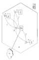
- FIG. 1illustrates a cell of a CDMA cellular communication system.
- FIGS. 2 and 3illustrate antenna structures for increasing antenna gain to which the teachings of the present invention can be applied.
- FIG. 4illustrates an antenna array wherein each antenna has a variable reactive load.
- FIGS. 5 and 6illustrate the dielectric ring in conjunction with the present invention.
- FIGS. 7 and 8illustrate a corrugated ground plane for producing a more directive antenna beam in accordance with the teachings of the present invention.
- FIGS. 9, 10 , 11 , 12 , 13 and 14illustrate an embodiment of the present invention including vertical gratings.
- FIG. 1illustrates one cell 50 of a typical CDMA cellular communication system.
- the cell 50represents a geographical area in which mobile subscriber units 60 - 1 through 60 - 3 communicate with a centrally located base station 65 .
- Each subscriber unit 60is equipped with an antenna 70 configured according to the present invention.
- the subscriber units 60are provided with wireless data and/or voice services by the system operator and can connect devices such as, for example, laptop computers, portable computers, personal digital assistants (PDAs) or the like through base station 65 (including the antenna 68 ) to a network 75 , which can be the public switched telephone network (PSTN), a packet switched computer network, such as the Internet, a public data network or a private intranet.
- PSTNpublic switched telephone network
- packet switched computer networksuch as the Internet, a public data network or a private intranet.
- the base station 65communicates with the network 75 over any number of different available communications protocols such as primary rate ISDN, or other LAPD based protocols such as IS-634 or V5.2, or even TCP/IP if the network 75 is a packet based Ethernet network such as the Internet.
- the subscriber units 60may be mobile in nature and may travel from one location to another while communicating with the base station 65 . As the subscriber units leave one cell and enter another, the communications link is handed off from the base station of the exiting cell to the base station of the entering cell.
- FIG. 1illustrates one base station 65 and three mobile subscriber units 60 in a cell 50 by way of example only and for ease of description of the invention.
- the inventionis applicable to systems in which there are typically many more subscriber units communicating with one or more base stations in an individual cell, such as the cell 50 .
- FIG. 1represents a standard cellular type communications system employing signaling schemes such as a CDMA, TDMA, GSM or others, in which the radio channels are assigned to carry data and/or voice between the base stations 65 and subscriber units 60 .
- FIG. 1is a CDMA-like system, using code division multiplexing principles such as those defined in the IS-95B standards for the air interface.
- the mobile subscriber units 60employ an antenna 70 that provides directional reception of forward link radio signals transmitted from the base station 65 , as well as directional transmission of reverse link signals (via a process called beam forming) from the mobile subscriber units 60 to the base station 65 .
- This conceptis illustrated in FIG. 1 by the example beam patterns 71 through 73 that extend outwardly from each mobile subscriber unit 60 more or less in a direction for best propagation toward the base station 65 .
- the antenna apparatus 70reduces the effects of intercell interference and multipath fading for the mobile subscriber units 60 .
- the antenna beam patterns 71 , 72 and 73extend outward in the direction of the base station 65 but are attenuated in most other directions, less power is required for transmission of effective communications signals from the mobile subscriber units 60 - 1 , 60 - 2 and 60 - 3 to the base station 65 .
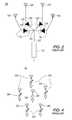
- FIG. 2One antenna array embodiment providing a directive beam pattern and further to which the teachings of the present invention can be applied, is illustrated in FIG. 2 .
- the FIG. 2 antenna array 100comprises a four-element circular array provided with four antenna elements 103 .
- a single-path networkfeeds each of the antenna elements 103 .
- the networkcomprises four fifty-ohm transmission lines 105 meeting at a junction 106 , with a 25-ohm transmission line 107 .
- Each of the antenna feed lines 105has a switch 108 interposed along the feed line.
- each switch 108is represented by a diode, although those skilled in the art recognize that other techniques can be employed, including the use of a single-pole-double-throw (SPDT) switch.
- SPDTsingle-pole-double-throw
- each of the antenna elements 103is independently controlled by its respective switch 108 .
- a 35-ohm quarter-wave transformer 110matches the 25-ohm transmission line 107 to the 50-ohm
- any adjacent pair of the switches 108can be closed to create the desired antenna beam pattern.
- the antenna array 100can also be scanned by successively opening and closing the adjacent pairs of switches 108 , changing the active elements of the antenna array 100 to effectuate the beam pattern movement.
- it is also possible to activate only one elementin which case the transition line 107 has a 50-ohm characteristic impedance and the quarter-wave transformer 110 is unnecessary.
- FIG. 3Another antenna design that presents an inexpensive, electrically small, low loss, low cost, medium directivity, electronically scanable antenna array is illustrated in FIG. 3 .
- This antenna array 130includes a single excited antenna element surrounded by electronically tunable passive elements that serve as directors or reflectors as desired.
- the antenna array 130includes a single central active element 132 surrounded by five passive reflector-directors 134 through 138 .
- the reflector-directors 134 - 138are also referred to as passive elements.
- the active element 132 and the passive elements 134 through 138are dipole antennas. As shown, the active element 132 is electrically connected to a fifty ohm transmission line 140 .
- Each passive element 134 through 138is attached to a single-pole double throw (SPDT) switch 160 .
- SPDTsingle-pole double throw
- the position of the switch 160places each of the passive elements 134 through 138 in either a directive or a reflective state.
- the antenna elementWhen in a directive state, the antenna element is virtually invisible to the radio frequency signal and therefore directs the radio frequency energy in the forward direction, in the reflective state the radio frequency energy is returned in the direction of the source.
- Each switch 160couples its respective passive element into one of two separate open or short-circuited transmission line stubs.
- the length of each transmission line stubis predetermined to generate the necessary reactive impedance for the passive elements 134 through 138 , such that the directive or reflective state is achieved.
- the reactive impedancecan also be realized through the use of an application-specific integrated circuit or a lumped reactive load.
- the antenna array 130When in use, the antenna array 130 provides a fixed beam directive pattern in the direction identified by the arrowhead 164 by placing the passive elements 134 , 137 and 138 in the reflective state while the passive elements 135 and 136 are switched to the directive state. Scanning of the beam is accomplished by progressively opening and closing adjacent switches 160 in the circle formed by the passive elements 134 through 138 . An omnidirectional mode is achieved when all of the passive elements 134 through 138 are placed in the directive state.
- the antenna array 130has N operating directive modes, where N is the number of passive elements.
- the fundamental array moderequires switching all of the N passive elements to the directive state to achieve an omnidirectional far-field pattern.
- Progressively increasing directivitycan be achieved by switching from one to approximately half the number of passive elements into the reflective state, while the remaining elements are directive.
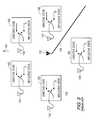
- FIG. 4illustrates an antenna array 198 comprising six vertical monopoles 200 arranged at an approximately equal radius (and having approximately equal angular spacing there between), from a center element 202 .
- the center elementis the active element, in the transmitting mode, as indicated by the alternating input signal referred to with reference character 206 .
- the active element 202functions in a reciprocal manner for signals transmitted to the antenna array 198 .
- the passive elements 200shape the radiation pattern from (or to) the active element 202 by selectively providing reflective or directive properties at their respective location. The reflective/directive properties or a combination of both is determined by the setting of the variable reactance element 204 associated with each of the passive elements 200 .
- the passive elements 200When the passive elements 200 are configured to serve as directors, the radiation transmitted by the active element 202 (or received by the active element 202 in the receive mode) passes through the ring of passive elements 200 to form an omnidirectional antenna beam pattern.
- the passive elements 200When the passive elements 200 are configured in the reflective mode, the radio frequency energy transmitted from the active element 202 is reflected back toward the center of the antenna ring.
- changing the resonant lengthcauses an antenna element to become reflective (when the element is longer than the resonant length, wherein the resonant length is defined as ⁇ /2 or ⁇ /4 if a ground plane is present) or directive/transparent (when the element is shorter than the resonant length).
- a continuous distribution of reflectors among the passive elements 200collimates the radiation pattern in the direction of those elements configured as directors.
- each of the passive elements 200 and the active element 202are oriented for vertical polarization of the transmitted or received signal. It is known to those skilled in the art that horizontal placement of the antenna elements results in horizontal signal polarization.
- the active element 202is replaced by a loop or annular ring antenna and the passive elements 202 are replaced by horizontal dipole antennas.
- the energy passing through the directive configured passive elements 200can be further shaped into a more directive antenna beam.
- the beamis shaped by placement of an annular dielectric substrate 210 around the antenna array 198 .
- the dielectric substrateis in the shape of a ring with an outer band defining an interior aperture, with the passive elements 200 and the active element 202 disposed within the interior aperture.
- the dielectric substrate 210is a slow wave structure having a lower propagation constant than air. As a result, the portion of the transmitted wave (or the received wave in the receive mode) that contacts the dielectric substrate 210 is guided and slowed relative to the free space portion of the wave.
- the slow-wave structureessentially guides the power or radiated energy along the dielectric slab to form a more directive beam.
- the radius of the dielectric substrate 210is at least a half wavelength.
- a slow wave structurecan take many forms, including a dielectric slab, a corrugated conducting surface, conductive gratings or any combination thereof.
- variable reactance elements 204are tuned to optimize operation of the passive elements 200 with the dielectric substrate 210 . For a given operational frequency, once the optimum distance between the passive elements 200 and the circumference of the interior aperture of the dielectric substrate 210 has been established, this distance remains unchanged during operation at the given frequency.
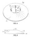
- FIG. 6illustrates the dielectric substrate 210 along cross section AA′ of FIG. 5 .
- the dielectric substrate 210includes two tapered edges 218 and 220 .
- a ground plane 222 below the dielectric substrate 210can also be seen in this view. Both of these tapered edges 218 and 220 edges ease the transition from air to substrate or vice versa. Abrupt transitions cause reflections of the incident wave which, in this situation, reduces the effect of the slow-wave structure.
- the tapers 218 and 220are shown of unequal length, those skilled in the art will recognize that a longer taper provides a more advantageous transition between the free space propagation constant and the dielectric propagation constant.
- the taper lengthis also dependent upon the space available for the dielectric slab 210 . Ideally, the tapers should be long if sufficient space is available for increasing the size of the dielectric substrate 210 .
- the height of the dielectric substrate 210is the wavelength of the received or transmitted signal divided by four (i.e., ⁇ /4). In an embodiment where the ground plane 222 is not present, the height of the dielectric slab 210 is ⁇ /2.
- the wavelength ⁇when considered in conjunction with the dielectric substrate 210 , is the wavelength in the dielectric, which is always less than the free space wavelength.
- the antenna directivityis a monotonic function of the dielectric substrate radius. A longer dielectric substrate 210 provides a gradual transition over which the radio frequency signal passes from the dielectric substrate 210 into free space (and vice versa for a received wave). This allows the wave to maintain collimation, which increases the antenna array directivity when the wave exits the dielectric substrate 210 . As known by those skilled in the art, generally, the antenna directivity is calculated in the far field where the wave front is substantially planar.
- the passive elements 200 , the active element 202 and the dielectric substrate 210are mounted on a platform or within a housing for placement on a work surface.
- a laptop computerfor example, to access the Internet via a CDMA wireless system with the passive elements 200 and the active element 202 fed and controlled by a wireless communications devices in the laptop.
- the antenna elements 200 and 202 and the dielectric substrate 210can also be integrated into a surface of the laptop computer such that the passive elements 200 and the active element 202 extend vertically above that surface.
- the dielectric substrate 210can be either integrated within that laptop surface or can be formed as a separate component for setting upon the surface in such a way so as to surround the passive elements 200 .
- the passive elements 200 and the active element 202can be foldably disposed so as to contact the surface when in a folded state and deployed into a vertical state for operation.
- the separate dielectric slab 210can be fitted around the passive elements 200 .
- the dielectric substrate 210can be fabricated using any low-loss dielectric material, including polystyrene, alumina, polyethylene or an artificial dielectric.
- an artificial dielectricis a volume filled with hollow metal spheres that are isolated from each other.
- FIG. 7illustrates an antenna array 230 , including a corrugated metal disk 250 surrounding the passive antenna elements 200 .
- the corrugated metal disk 250which offers similar gain-improving functionality as the dielectric substrate 210 in FIG. 5, comprises a plurality of circumferential mesas 252 defining grooves 254 there between.
- FIG. 8is a view through section AA′ of FIG. 7 . Note that the innermost mesa 252 A includes a tapered surface 256 . Also, the outermost mesas 252 B and 252 C include tapered surfaces 258 and 260 , respectively. As in the FIG. 5 embodiment, the tapers 256 and 258 provide a transition region between free space and the propagation constant presented by the corrugated metal disk 250 .
- the corrugated metal disk 250serves as a slow-wave structure because the grooves 254 are approximately a quarter-wavelength deep and therefore present an impedance to the traveling radio frequency signal that approximates an open, i.e., a quarter-wavelength in free space.
- the impedancecauses bending of the traveling wave in a manner similar to the bending caused by the dielectric substrate 210 of FIG. 5 . If the grooves 254 were to provide a perfect open, no radio frequency energy would be trapped by the groove and there would be no bending of the wave.
- the key to successful utilization of the FIG. 7 embodimentis the trapping of the radio frequency wave.
- the grooves 254When the grooves 254 are shallow, they release the wave and thus the contouring (i.e., the location of the mesas and grooves) controls the location and degree to which the wave is allowed to radiate to form a collimated wave front. For example, if the grooves were radially oriented, the wave would simply travel along the grooves and could not be controlled.
- FIGS. 7 and 8 embodimentsillustrate only three grooves or notches, it is known by those skilled in the art that additional grooves or notches can be provided to further control the traveling radio frequency wave and improve the directivity of the antenna in the azimuth direction.
- FIG. 9illustrates an antenna array 258 representing another embodiment of the present invention, including a ground plane 260 and the previously discussed active element 202 and the passive elements 200 . Additionally, FIG. 9 illustrates a plurality of parasitic conductive gratings 262 . In the embodiment of FIG. 9, the parasitic conductive gratings 262 are shown as spaced apart from and along the same radial lines as the passive elements 200 . In a sense, the antenna array 258 of FIG. 9 is a special case of the antenna array 230 of FIG. 7 . The height of the circumferential mesas 252 is represented by the position of the parasitic conductive gratings 262 . The taper of the outer mesas 252 B and 252 C in FIG. 8 is repeated by tapering the parasitic conductive gratings 262 in the direction away from the center element 202 .
- FIG. 10illustrates the antenna array 258 in cross section along the lines AA′.
- Exemplary lengths for the passive elements 200 and the active element 202are also shown in FIG. 10 .
- exemplary height and spacings between the parasitic conductive gratings 262 at 1.9 GHzare also set forth. Generally, the spacing is 0.9 ⁇ to 0.28 ⁇ .
- the spacing between the active element 202 , the passive elements 200 , and the plurality of parasitic conductive gratings 262are generally tied to the height of each element. If the passive elements 200 and the plurality of parasitic conductive gratings 262 are a resonant length, the element simply resonates and thereby retains the received energy. Some energy may spill over to neighboring elements.
- the impedance of the elementcauses it to act as a forward scatterer due to the imparted phase advance.
- Scatteringis the process by which a radiating wave strikes an obstacle, and then re-radiates in all directions. If the scattering is predominant in the forward direction of the traveling wave, then the scattering is referred to as forward scattering.
- the elementis longer than a resonant length, the resulting phase retardation interacts with the original traveling wave thereby reducing or even canceling the forward travelling radiation. As a result, the energy is scattered backwards. That is, the element acts as a reflector. In the FIG.
- the plurality of parasitic conductive gratings 262can be either shorted to the ground plane 260 or adjustably reactively loaded, where the loading effectively adjusts the effective length of any one of the plurality of parasitic conductive gratings 262 causing the parasitic conductive grating 262 to have a length equal to, less than or greater than the resonant length, with the resulting directive or reflective effects as discussed above.
- Providing this controllable reactive featureprovides the ability to vary the degree of directivity or beam pattern width as desired.
- the ground plane 260is pentagonal in shape. In another embodiment, the ground plane can be circular. In one embodiment, the number of facets in the ground plane 260 is equal to the number of passive elements. As in the embodiments of FIGS. 5 and 7, the plurality of gratings or parasitic conductive elements 262 serve to slow down the radio frequency wave and thus improve the directivity in the azimuth direction. Adding more gratings causes further reductions in the RF energy in the elevation direction.
- the beam pattern produced by the antenna array 258includes five individual and highly directive lobes when each of the passive elements 200 is placed in the directive state. When two adjacent passive elements 200 are placed in a directive state, the highly directive lobe formed is in a direction between the two directive elements. When all passive elements 200 are placed in a directive state simultaneously, an omni-directional pancake pattern is created.
- the parasitic conductive gratings 262 of FIG. 9have sharper resonance peaks and therefore are very efficient in slowing down the traveling RF wave.
- the parasitic conductive gratings 262are not spaced at precisely the resonant frequency. Instead, a residual resonance is created that causes the slow-down effect in the radio frequency signal.
- the antenna array 270 of FIG. 1includes the elements of FIG. 9, with the addition of a plurality of interstitial parasitic elements 270 between the parasitic conductive gratings 262 , to further guide and shape the radiation pattern.
- the interstitial parasitic elements 270are shorted to the ground plane 260 and provide additional refinement of the beam pattern.
- the interstitial parasitic elements 270are placed experimentally to afford one or more of the following objectives: reducing the ripple in the omnidirectional pattern, adding intermediate high-gain beam positions when the array is steered through the resonant characteristic of the parasitic elements 200 , reducing undesirable side lobes and improving the front to back power ratio.
- an antenna constructed according to the teachings of FIG. 11has a peak directivity of 8.5 to 9.5 dBi over a bandwidth of thirty percent.
- this high-gain antenna beamcan also be steered.
- an omnidirectional beam substantially in the azimuth planeis formed.
- the peak directivitywas measured at 5.6 to 7.1 (dBi) over the same frequency band as the directive mode.
- the FIG. 11 embodimentprovides both a high-gain omnidirectional pattern and a high-gain steerable beam pattern.
- the approximate height of the interstitial parasitic elements 270is 1.5 inches and the distance from the active element 202 to the outer interstitial parasitic elements 270 is approximately 7.6 inches.
- the antenna array of FIG. 12is derived from FIG. 9, where the parasitic conductive gratings 262 and the passive elements 200 are integrated into or disposed on a dielectric substrate or printed circuit board 280 .
- the passive elements 200 and the parasitic conductive gratings 262are fabricated individually.
- the passive elements 200are separated from the ground plane 260 by an insulating material and conductively connected to the reactance control elements previously discussed.
- the parasitic conductive gratings 262are shorted directly to the ground plane 260 or controllably reactively loaded as discussed above.
- the process of fabricating the FIG. 9 embodimentis time intensive.
- the FIG. 9is time intensive.
- the FIG. 12 embodimentis therefore especially advantageous because the parasitic conductive gratings 262 and the passive elements 200 are printed on or etched from a dielectric substrate or printed circuit board material. This process of integrating and grouping the various antenna elements as shown, provides additional mechanical strength and improved manufacturing precision with respect to the height and spacing of the elements. Due to the use of a dielectric material between the various antenna elements, the FIG. 12 embodiment can be considered a hybrid between the dielectric substrate embodiment of FIG. 5 and the conductive grating embodiment of FIG. 9 . In particular, the dielectric substrate 280 smooths out the discrete resonant properties of the parasitic conductive gratings 262 , thereby reducing the formation of gain spikes in the frequency spectrum of the operational bandwidth.
- FIG. 13illustrates another process for fabricating the antenna array 258 of FIG. 9 and the antenna array 270 of FIG. 11 .
- the parasitic conductive gratings 262(and the interstitial parasitic elements 270 in FIG. 11) are stamped from the ground plane 260 and then bent upwardly to form the parasitic conductive gratings 262 (and the interstitial parasitic elements 270 in FIG. 11 ).
- This processis illustrated in greater detail in the enlarged view of FIG. 14 .
- the parasitic conductive gratings 262 the interstitial parasitic elements 270are formed by creating a U-shaped slot in the in the ground plane 260 such that a deformable joint is defined by the slot.
- the parasitic elementsare then formed by upwardly bending that region of the ground plane 260 defined by the slot along the deformable joint.
- the void remaining after stamping three sides of the ground plane 260is referred to by reference character 270 . It has been found that the void 270 does not significantly affect the performance of the antenna array 258 (FIG. 9) and 270 (FIG. 11 ).
- the active element 202 and the passive elements 200are formed on a separate metallic disc 280 , which is attached to the ground plane 260 using screws or other fasteners 282 .
Landscapes
- Variable-Direction Aerials And Aerial Arrays (AREA)
Abstract
Description
Claims (34)
Priority Applications (3)
| Application Number | Priority Date | Filing Date | Title |
|---|---|---|---|
| US09/845,133US6606057B2 (en) | 2001-04-30 | 2001-04-30 | High gain planar scanned antenna array |
| US10/444,322US6864852B2 (en) | 2001-04-30 | 2003-05-23 | High gain antenna for wireless applications |
| US11/063,118US7088306B2 (en) | 2001-04-30 | 2005-02-22 | High gain antenna for wireless applications |
Applications Claiming Priority (1)
| Application Number | Priority Date | Filing Date | Title |
|---|---|---|---|
| US09/845,133US6606057B2 (en) | 2001-04-30 | 2001-04-30 | High gain planar scanned antenna array |
Related Child Applications (1)
| Application Number | Title | Priority Date | Filing Date |
|---|---|---|---|
| US10/444,322Continuation-In-PartUS6864852B2 (en) | 2001-04-30 | 2003-05-23 | High gain antenna for wireless applications |
Publications (2)
| Publication Number | Publication Date |
|---|---|
| US20020158798A1 US20020158798A1 (en) | 2002-10-31 |
| US6606057B2true US6606057B2 (en) | 2003-08-12 |
Family
ID=25294497
Family Applications (1)
| Application Number | Title | Priority Date | Filing Date |
|---|---|---|---|
| US09/845,133Expired - LifetimeUS6606057B2 (en) | 2001-04-30 | 2001-04-30 | High gain planar scanned antenna array |
Country Status (1)
| Country | Link |
|---|---|
| US (1) | US6606057B2 (en) |
Cited By (162)
| Publication number | Priority date | Publication date | Assignee | Title |
|---|---|---|---|---|
| US20030105099A1 (en)* | 2000-12-22 | 2003-06-05 | Michael Graupe | Novel compounds and compositions as cathepsin inhibitors |
| US20030117322A1 (en)* | 2001-12-26 | 2003-06-26 | Accton Technology Corporation | Twin monopole antenna |
| US20030184492A1 (en)* | 2001-11-09 | 2003-10-02 | Tantivy Communications, Inc. | Dual band phased array employing spatial second harmonics |
| US20040027304A1 (en)* | 2001-04-30 | 2004-02-12 | Bing Chiang | High gain antenna for wireless applications |
| US6741208B1 (en)* | 2003-05-06 | 2004-05-25 | Rockwell Collins | Dual-mode switched aperture/weather radar antenna array feed |
| US20040150568A1 (en)* | 2002-02-01 | 2004-08-05 | Tantivy Communications, Inc. | Aperiodic array antenna |
| US20040160373A1 (en)* | 2003-02-06 | 2004-08-19 | Fuba Automotive Gmbh & Co. Kg | Antenna having a monopole design, for use in several wireless communication services |
| US6816128B1 (en)* | 2003-06-25 | 2004-11-09 | Rockwell Collins | Pressurized antenna for electronic warfare sensors and jamming equipment |
| US20050057394A1 (en)* | 2003-09-15 | 2005-03-17 | Lg Telecom, Ltd. | Beam switching antenna system and method and apparatus for controlling the same |
| US20050162327A1 (en)* | 2004-01-23 | 2005-07-28 | Sony Corporation | Antenna apparatus |
| US20050162328A1 (en)* | 2004-01-23 | 2005-07-28 | Sony Corporation | Antenna apparatus |
| US20050179605A1 (en)* | 2004-02-16 | 2005-08-18 | Advanced Telecommunications Research Institute International | Array antenna apparatus capable of switching direction attaining low gain |
| US20050206573A1 (en)* | 2004-02-03 | 2005-09-22 | Advanced Telecommunications Research Institute International | Array antenna capable of controlling antenna characteristic |
| US20060079185A1 (en)* | 2001-01-31 | 2006-04-13 | Matsushita Electric Industrial Co., Ltd. | Radio communication system, mobile terminal unit thereof, and azimuth determining method |
| US20060227062A1 (en)* | 2005-04-06 | 2006-10-12 | The Boeing Company | Antenna system with parasitic element and associated method |
| US20070152892A1 (en)* | 2002-03-14 | 2007-07-05 | Ipr Licensing, Inc. | Mobile communication handset with adaptive antenna array |
| US20080136718A1 (en)* | 2006-12-08 | 2008-06-12 | Tietjen Byron W | Mobile radar array |
| US7522095B1 (en) | 2005-07-15 | 2009-04-21 | Lockheed Martin Corporation | Polygonal cylinder array antenna |
| US20100045553A1 (en)* | 2007-01-12 | 2010-02-25 | Masataka Ohira | Low-profile antenna structure |
| US20100056212A1 (en)* | 2005-05-31 | 2010-03-04 | Research In Motion Limited | Mobile wireless communications device comprising a satellite positioning system antenna and electrically conductive director element therefor |
| US20100156743A1 (en)* | 2008-12-24 | 2010-06-24 | Fujitsu Component Limited | Antenna device |
| CN1853315B (en)* | 2003-09-15 | 2011-10-12 | Lg电信株式会社 | Beam switching antenna system and method and apparatus for controlling the same |
| US9263798B1 (en)* | 2015-04-30 | 2016-02-16 | Adant Technologies, Inc. | Reconfigurable antenna apparatus |
| US9608740B2 (en) | 2015-07-15 | 2017-03-28 | At&T Intellectual Property I, L.P. | Method and apparatus for launching a wave mode that mitigates interference |
| US9640850B2 (en) | 2015-06-25 | 2017-05-02 | At&T Intellectual Property I, L.P. | Methods and apparatus for inducing a non-fundamental wave mode on a transmission medium |
| US9667317B2 (en) | 2015-06-15 | 2017-05-30 | At&T Intellectual Property I, L.P. | Method and apparatus for providing security using network traffic adjustments |
| US9674711B2 (en) | 2013-11-06 | 2017-06-06 | At&T Intellectual Property I, L.P. | Surface-wave communications and methods thereof |
| US9685992B2 (en) | 2014-10-03 | 2017-06-20 | At&T Intellectual Property I, L.P. | Circuit panel network and methods thereof |
| US9705610B2 (en) | 2014-10-21 | 2017-07-11 | At&T Intellectual Property I, L.P. | Transmission device with impairment compensation and methods for use therewith |
| US9705561B2 (en) | 2015-04-24 | 2017-07-11 | At&T Intellectual Property I, L.P. | Directional coupling device and methods for use therewith |
| US9722318B2 (en) | 2015-07-14 | 2017-08-01 | At&T Intellectual Property I, L.P. | Method and apparatus for coupling an antenna to a device |
| US9729197B2 (en) | 2015-10-01 | 2017-08-08 | At&T Intellectual Property I, L.P. | Method and apparatus for communicating network management traffic over a network |
| US9735833B2 (en) | 2015-07-31 | 2017-08-15 | At&T Intellectual Property I, L.P. | Method and apparatus for communications management in a neighborhood network |
| US9742521B2 (en) | 2014-11-20 | 2017-08-22 | At&T Intellectual Property I, L.P. | Transmission device with mode division multiplexing and methods for use therewith |
| US9742462B2 (en) | 2014-12-04 | 2017-08-22 | At&T Intellectual Property I, L.P. | Transmission medium and communication interfaces and methods for use therewith |
| US9748626B2 (en) | 2015-05-14 | 2017-08-29 | At&T Intellectual Property I, L.P. | Plurality of cables having different cross-sectional shapes which are bundled together to form a transmission medium |
| US9749013B2 (en) | 2015-03-17 | 2017-08-29 | At&T Intellectual Property I, L.P. | Method and apparatus for reducing attenuation of electromagnetic waves guided by a transmission medium |
| US9749053B2 (en) | 2015-07-23 | 2017-08-29 | At&T Intellectual Property I, L.P. | Node device, repeater and methods for use therewith |
| US9762289B2 (en) | 2014-10-14 | 2017-09-12 | At&T Intellectual Property I, L.P. | Method and apparatus for transmitting or receiving signals in a transportation system |
| US9769020B2 (en) | 2014-10-21 | 2017-09-19 | At&T Intellectual Property I, L.P. | Method and apparatus for responding to events affecting communications in a communication network |
| US9769128B2 (en) | 2015-09-28 | 2017-09-19 | At&T Intellectual Property I, L.P. | Method and apparatus for encryption of communications over a network |
| US9768833B2 (en) | 2014-09-15 | 2017-09-19 | At&T Intellectual Property I, L.P. | Method and apparatus for sensing a condition in a transmission medium of electromagnetic waves |
| US9780834B2 (en) | 2014-10-21 | 2017-10-03 | At&T Intellectual Property I, L.P. | Method and apparatus for transmitting electromagnetic waves |
| US9788326B2 (en) | 2012-12-05 | 2017-10-10 | At&T Intellectual Property I, L.P. | Backhaul link for distributed antenna system |
| US9787412B2 (en) | 2015-06-25 | 2017-10-10 | At&T Intellectual Property I, L.P. | Methods and apparatus for inducing a fundamental wave mode on a transmission medium |
| US9793951B2 (en) | 2015-07-15 | 2017-10-17 | At&T Intellectual Property I, L.P. | Method and apparatus for launching a wave mode that mitigates interference |
| US9793955B2 (en) | 2015-04-24 | 2017-10-17 | At&T Intellectual Property I, Lp | Passive electrical coupling device and methods for use therewith |
| US9793954B2 (en) | 2015-04-28 | 2017-10-17 | At&T Intellectual Property I, L.P. | Magnetic coupling device and methods for use therewith |
| US9800327B2 (en) | 2014-11-20 | 2017-10-24 | At&T Intellectual Property I, L.P. | Apparatus for controlling operations of a communication device and methods thereof |
| US9820146B2 (en) | 2015-06-12 | 2017-11-14 | At&T Intellectual Property I, L.P. | Method and apparatus for authentication and identity management of communicating devices |
| US9838078B2 (en) | 2015-07-31 | 2017-12-05 | At&T Intellectual Property I, L.P. | Method and apparatus for exchanging communication signals |
| US9838896B1 (en) | 2016-12-09 | 2017-12-05 | At&T Intellectual Property I, L.P. | Method and apparatus for assessing network coverage |
| US9847850B2 (en) | 2014-10-14 | 2017-12-19 | At&T Intellectual Property I, L.P. | Method and apparatus for adjusting a mode of communication in a communication network |
| US9847566B2 (en) | 2015-07-14 | 2017-12-19 | At&T Intellectual Property I, L.P. | Method and apparatus for adjusting a field of a signal to mitigate interference |
| US9853342B2 (en) | 2015-07-14 | 2017-12-26 | At&T Intellectual Property I, L.P. | Dielectric transmission medium connector and methods for use therewith |
| US9860075B1 (en) | 2016-08-26 | 2018-01-02 | At&T Intellectual Property I, L.P. | Method and communication node for broadband distribution |
| US9866276B2 (en) | 2014-10-10 | 2018-01-09 | At&T Intellectual Property I, L.P. | Method and apparatus for arranging communication sessions in a communication system |
| US9865911B2 (en) | 2015-06-25 | 2018-01-09 | At&T Intellectual Property I, L.P. | Waveguide system for slot radiating first electromagnetic waves that are combined into a non-fundamental wave mode second electromagnetic wave on a transmission medium |
| US9866309B2 (en) | 2015-06-03 | 2018-01-09 | At&T Intellectual Property I, Lp | Host node device and methods for use therewith |
| US9871282B2 (en) | 2015-05-14 | 2018-01-16 | At&T Intellectual Property I, L.P. | At least one transmission medium having a dielectric surface that is covered at least in part by a second dielectric |
| US9871558B2 (en) | 2014-10-21 | 2018-01-16 | At&T Intellectual Property I, L.P. | Guided-wave transmission device and methods for use therewith |
| US9871283B2 (en) | 2015-07-23 | 2018-01-16 | At&T Intellectual Property I, Lp | Transmission medium having a dielectric core comprised of plural members connected by a ball and socket configuration |
| US9876570B2 (en) | 2015-02-20 | 2018-01-23 | At&T Intellectual Property I, Lp | Guided-wave transmission device with non-fundamental mode propagation and methods for use therewith |
| US9876264B2 (en) | 2015-10-02 | 2018-01-23 | At&T Intellectual Property I, Lp | Communication system, guided wave switch and methods for use therewith |
| US9876605B1 (en) | 2016-10-21 | 2018-01-23 | At&T Intellectual Property I, L.P. | Launcher and coupling system to support desired guided wave mode |
| US9882257B2 (en) | 2015-07-14 | 2018-01-30 | At&T Intellectual Property I, L.P. | Method and apparatus for launching a wave mode that mitigates interference |
| US9887447B2 (en) | 2015-05-14 | 2018-02-06 | At&T Intellectual Property I, L.P. | Transmission medium having multiple cores and methods for use therewith |
| US9893795B1 (en) | 2016-12-07 | 2018-02-13 | At&T Intellectual Property I, Lp | Method and repeater for broadband distribution |
| US9906269B2 (en) | 2014-09-17 | 2018-02-27 | At&T Intellectual Property I, L.P. | Monitoring and mitigating conditions in a communication network |
| US9912419B1 (en) | 2016-08-24 | 2018-03-06 | At&T Intellectual Property I, L.P. | Method and apparatus for managing a fault in a distributed antenna system |
| US9912033B2 (en) | 2014-10-21 | 2018-03-06 | At&T Intellectual Property I, Lp | Guided wave coupler, coupling module and methods for use therewith |
| US9912027B2 (en) | 2015-07-23 | 2018-03-06 | At&T Intellectual Property I, L.P. | Method and apparatus for exchanging communication signals |
| US9912381B2 (en) | 2015-06-03 | 2018-03-06 | At&T Intellectual Property I, Lp | Network termination and methods for use therewith |
| US9913139B2 (en) | 2015-06-09 | 2018-03-06 | At&T Intellectual Property I, L.P. | Signal fingerprinting for authentication of communicating devices |
| US9911020B1 (en) | 2016-12-08 | 2018-03-06 | At&T Intellectual Property I, L.P. | Method and apparatus for tracking via a radio frequency identification device |
| US9917341B2 (en) | 2015-05-27 | 2018-03-13 | At&T Intellectual Property I, L.P. | Apparatus and method for launching electromagnetic waves and for modifying radial dimensions of the propagating electromagnetic waves |
| US9929755B2 (en) | 2015-07-14 | 2018-03-27 | At&T Intellectual Property I, L.P. | Method and apparatus for coupling an antenna to a device |
| US9927517B1 (en) | 2016-12-06 | 2018-03-27 | At&T Intellectual Property I, L.P. | Apparatus and methods for sensing rainfall |
| US9930668B2 (en) | 2013-05-31 | 2018-03-27 | At&T Intellectual Property I, L.P. | Remote distributed antenna system |
| US9948333B2 (en) | 2015-07-23 | 2018-04-17 | At&T Intellectual Property I, L.P. | Method and apparatus for wireless communications to mitigate interference |
| US9948354B2 (en) | 2015-04-28 | 2018-04-17 | At&T Intellectual Property I, L.P. | Magnetic coupling device with reflective plate and methods for use therewith |
| US9948355B2 (en) | 2014-10-21 | 2018-04-17 | At&T Intellectual Property I, L.P. | Apparatus for providing communication services and methods thereof |
| US9954286B2 (en) | 2014-10-21 | 2018-04-24 | At&T Intellectual Property I, L.P. | Guided-wave transmission device with non-fundamental mode propagation and methods for use therewith |
| US9954287B2 (en) | 2014-11-20 | 2018-04-24 | At&T Intellectual Property I, L.P. | Apparatus for converting wireless signals and electromagnetic waves and methods thereof |
| US9967173B2 (en) | 2015-07-31 | 2018-05-08 | At&T Intellectual Property I, L.P. | Method and apparatus for authentication and identity management of communicating devices |
| US9973416B2 (en) | 2014-10-02 | 2018-05-15 | At&T Intellectual Property I, L.P. | Method and apparatus that provides fault tolerance in a communication network |
| US9973940B1 (en) | 2017-02-27 | 2018-05-15 | At&T Intellectual Property I, L.P. | Apparatus and methods for dynamic impedance matching of a guided wave launcher |
| US9991580B2 (en) | 2016-10-21 | 2018-06-05 | At&T Intellectual Property I, L.P. | Launcher and coupling system for guided wave mode cancellation |
| US9999038B2 (en) | 2013-05-31 | 2018-06-12 | At&T Intellectual Property I, L.P. | Remote distributed antenna system |
| US9998870B1 (en) | 2016-12-08 | 2018-06-12 | At&T Intellectual Property I, L.P. | Method and apparatus for proximity sensing |
| US9997819B2 (en) | 2015-06-09 | 2018-06-12 | At&T Intellectual Property I, L.P. | Transmission medium and method for facilitating propagation of electromagnetic waves via a core |
| US10009067B2 (en) | 2014-12-04 | 2018-06-26 | At&T Intellectual Property I, L.P. | Method and apparatus for configuring a communication interface |
| US10009063B2 (en) | 2015-09-16 | 2018-06-26 | At&T Intellectual Property I, L.P. | Method and apparatus for use with a radio distributed antenna system having an out-of-band reference signal |
| US10020844B2 (en) | 2016-12-06 | 2018-07-10 | T&T Intellectual Property I, L.P. | Method and apparatus for broadcast communication via guided waves |
| US10027397B2 (en) | 2016-12-07 | 2018-07-17 | At&T Intellectual Property I, L.P. | Distributed antenna system and methods for use therewith |
| US10027398B2 (en) | 2015-06-11 | 2018-07-17 | At&T Intellectual Property I, Lp | Repeater and methods for use therewith |
| US10033108B2 (en) | 2015-07-14 | 2018-07-24 | At&T Intellectual Property I, L.P. | Apparatus and methods for generating an electromagnetic wave having a wave mode that mitigates interference |
| US10044409B2 (en) | 2015-07-14 | 2018-08-07 | At&T Intellectual Property I, L.P. | Transmission medium and methods for use therewith |
| US10069535B2 (en) | 2016-12-08 | 2018-09-04 | At&T Intellectual Property I, L.P. | Apparatus and methods for launching electromagnetic waves having a certain electric field structure |
| US10079661B2 (en) | 2015-09-16 | 2018-09-18 | At&T Intellectual Property I, L.P. | Method and apparatus for use with a radio distributed antenna system having a clock reference |
| US10090606B2 (en) | 2015-07-15 | 2018-10-02 | At&T Intellectual Property I, L.P. | Antenna system with dielectric array and methods for use therewith |
| US10090594B2 (en) | 2016-11-23 | 2018-10-02 | At&T Intellectual Property I, L.P. | Antenna system having structural configurations for assembly |
| US10103801B2 (en) | 2015-06-03 | 2018-10-16 | At&T Intellectual Property I, L.P. | Host node device and methods for use therewith |
| US10103422B2 (en) | 2016-12-08 | 2018-10-16 | At&T Intellectual Property I, L.P. | Method and apparatus for mounting network devices |
| US10136434B2 (en) | 2015-09-16 | 2018-11-20 | At&T Intellectual Property I, L.P. | Method and apparatus for use with a radio distributed antenna system having an ultra-wideband control channel |
| US10135146B2 (en) | 2016-10-18 | 2018-11-20 | At&T Intellectual Property I, L.P. | Apparatus and methods for launching guided waves via circuits |
| US10135145B2 (en) | 2016-12-06 | 2018-11-20 | At&T Intellectual Property I, L.P. | Apparatus and methods for generating an electromagnetic wave along a transmission medium |
| US10135147B2 (en) | 2016-10-18 | 2018-11-20 | At&T Intellectual Property I, L.P. | Apparatus and methods for launching guided waves via an antenna |
| US10139820B2 (en) | 2016-12-07 | 2018-11-27 | At&T Intellectual Property I, L.P. | Method and apparatus for deploying equipment of a communication system |
| US10148016B2 (en) | 2015-07-14 | 2018-12-04 | At&T Intellectual Property I, L.P. | Apparatus and methods for communicating utilizing an antenna array |
| US10144036B2 (en) | 2015-01-30 | 2018-12-04 | At&T Intellectual Property I, L.P. | Method and apparatus for mitigating interference affecting a propagation of electromagnetic waves guided by a transmission medium |
| US10168695B2 (en) | 2016-12-07 | 2019-01-01 | At&T Intellectual Property I, L.P. | Method and apparatus for controlling an unmanned aircraft |
| US10170840B2 (en) | 2015-07-14 | 2019-01-01 | At&T Intellectual Property I, L.P. | Apparatus and methods for sending or receiving electromagnetic signals |
| US10178445B2 (en) | 2016-11-23 | 2019-01-08 | At&T Intellectual Property I, L.P. | Methods, devices, and systems for load balancing between a plurality of waveguides |
| US10205655B2 (en) | 2015-07-14 | 2019-02-12 | At&T Intellectual Property I, L.P. | Apparatus and methods for communicating utilizing an antenna array and multiple communication paths |
| US10224634B2 (en) | 2016-11-03 | 2019-03-05 | At&T Intellectual Property I, L.P. | Methods and apparatus for adjusting an operational characteristic of an antenna |
| US10225025B2 (en) | 2016-11-03 | 2019-03-05 | At&T Intellectual Property I, L.P. | Method and apparatus for detecting a fault in a communication system |
| US10243270B2 (en) | 2016-12-07 | 2019-03-26 | At&T Intellectual Property I, L.P. | Beam adaptive multi-feed dielectric antenna system and methods for use therewith |
| US10243784B2 (en) | 2014-11-20 | 2019-03-26 | At&T Intellectual Property I, L.P. | System for generating topology information and methods thereof |
| US10264586B2 (en) | 2016-12-09 | 2019-04-16 | At&T Mobility Ii Llc | Cloud-based packet controller and methods for use therewith |
| US10291334B2 (en) | 2016-11-03 | 2019-05-14 | At&T Intellectual Property I, L.P. | System for detecting a fault in a communication system |
| US10291311B2 (en) | 2016-09-09 | 2019-05-14 | At&T Intellectual Property I, L.P. | Method and apparatus for mitigating a fault in a distributed antenna system |
| US10298293B2 (en) | 2017-03-13 | 2019-05-21 | At&T Intellectual Property I, L.P. | Apparatus of communication utilizing wireless network devices |
| US10305190B2 (en) | 2016-12-01 | 2019-05-28 | At&T Intellectual Property I, L.P. | Reflecting dielectric antenna system and methods for use therewith |
| US10312567B2 (en) | 2016-10-26 | 2019-06-04 | At&T Intellectual Property I, L.P. | Launcher with planar strip antenna and methods for use therewith |
| US10320586B2 (en) | 2015-07-14 | 2019-06-11 | At&T Intellectual Property I, L.P. | Apparatus and methods for generating non-interfering electromagnetic waves on an insulated transmission medium |
| US10326494B2 (en) | 2016-12-06 | 2019-06-18 | At&T Intellectual Property I, L.P. | Apparatus for measurement de-embedding and methods for use therewith |
| US10326689B2 (en) | 2016-12-08 | 2019-06-18 | At&T Intellectual Property I, L.P. | Method and system for providing alternative communication paths |
| US10340573B2 (en) | 2016-10-26 | 2019-07-02 | At&T Intellectual Property I, L.P. | Launcher with cylindrical coupling device and methods for use therewith |
| US10341142B2 (en) | 2015-07-14 | 2019-07-02 | At&T Intellectual Property I, L.P. | Apparatus and methods for generating non-interfering electromagnetic waves on an uninsulated conductor |
| US10340983B2 (en) | 2016-12-09 | 2019-07-02 | At&T Intellectual Property I, L.P. | Method and apparatus for surveying remote sites via guided wave communications |
| US10340603B2 (en) | 2016-11-23 | 2019-07-02 | At&T Intellectual Property I, L.P. | Antenna system having shielded structural configurations for assembly |
| US10340601B2 (en) | 2016-11-23 | 2019-07-02 | At&T Intellectual Property I, L.P. | Multi-antenna system and methods for use therewith |
| US10340600B2 (en) | 2016-10-18 | 2019-07-02 | At&T Intellectual Property I, L.P. | Apparatus and methods for launching guided waves via plural waveguide systems |
| US10355367B2 (en) | 2015-10-16 | 2019-07-16 | At&T Intellectual Property I, L.P. | Antenna structure for exchanging wireless signals |
| US10361489B2 (en) | 2016-12-01 | 2019-07-23 | At&T Intellectual Property I, L.P. | Dielectric dish antenna system and methods for use therewith |
| US10359749B2 (en) | 2016-12-07 | 2019-07-23 | At&T Intellectual Property I, L.P. | Method and apparatus for utilities management via guided wave communication |
| US10374316B2 (en) | 2016-10-21 | 2019-08-06 | At&T Intellectual Property I, L.P. | System and dielectric antenna with non-uniform dielectric |
| US10382976B2 (en) | 2016-12-06 | 2019-08-13 | At&T Intellectual Property I, L.P. | Method and apparatus for managing wireless communications based on communication paths and network device positions |
| US10389037B2 (en) | 2016-12-08 | 2019-08-20 | At&T Intellectual Property I, L.P. | Apparatus and methods for selecting sections of an antenna array and use therewith |
| US10389029B2 (en) | 2016-12-07 | 2019-08-20 | At&T Intellectual Property I, L.P. | Multi-feed dielectric antenna system with core selection and methods for use therewith |
| US10411356B2 (en) | 2016-12-08 | 2019-09-10 | At&T Intellectual Property I, L.P. | Apparatus and methods for selectively targeting communication devices with an antenna array |
| US10439675B2 (en) | 2016-12-06 | 2019-10-08 | At&T Intellectual Property I, L.P. | Method and apparatus for repeating guided wave communication signals |
| US10446936B2 (en) | 2016-12-07 | 2019-10-15 | At&T Intellectual Property I, L.P. | Multi-feed dielectric antenna system and methods for use therewith |
| US10498044B2 (en) | 2016-11-03 | 2019-12-03 | At&T Intellectual Property I, L.P. | Apparatus for configuring a surface of an antenna |
| US10530505B2 (en) | 2016-12-08 | 2020-01-07 | At&T Intellectual Property I, L.P. | Apparatus and methods for launching electromagnetic waves along a transmission medium |
| US10535928B2 (en) | 2016-11-23 | 2020-01-14 | At&T Intellectual Property I, L.P. | Antenna system and methods for use therewith |
| US10547348B2 (en) | 2016-12-07 | 2020-01-28 | At&T Intellectual Property I, L.P. | Method and apparatus for switching transmission mediums in a communication system |
| US10601494B2 (en) | 2016-12-08 | 2020-03-24 | At&T Intellectual Property I, L.P. | Dual-band communication device and method for use therewith |
| US10637149B2 (en) | 2016-12-06 | 2020-04-28 | At&T Intellectual Property I, L.P. | Injection molded dielectric antenna and methods for use therewith |
| US10650940B2 (en) | 2015-05-15 | 2020-05-12 | At&T Intellectual Property I, L.P. | Transmission medium having a conductive material and methods for use therewith |
| US10694379B2 (en) | 2016-12-06 | 2020-06-23 | At&T Intellectual Property I, L.P. | Waveguide system with device-based authentication and methods for use therewith |
| US10727599B2 (en) | 2016-12-06 | 2020-07-28 | At&T Intellectual Property I, L.P. | Launcher with slot antenna and methods for use therewith |
| US10755542B2 (en) | 2016-12-06 | 2020-08-25 | At&T Intellectual Property I, L.P. | Method and apparatus for surveillance via guided wave communication |
| US10777873B2 (en) | 2016-12-08 | 2020-09-15 | At&T Intellectual Property I, L.P. | Method and apparatus for mounting network devices |
| US10797781B2 (en) | 2015-06-03 | 2020-10-06 | At&T Intellectual Property I, L.P. | Client node device and methods for use therewith |
| US10811767B2 (en) | 2016-10-21 | 2020-10-20 | At&T Intellectual Property I, L.P. | System and dielectric antenna with convex dielectric radome |
| US10819035B2 (en) | 2016-12-06 | 2020-10-27 | At&T Intellectual Property I, L.P. | Launcher with helical antenna and methods for use therewith |
| US10916969B2 (en) | 2016-12-08 | 2021-02-09 | At&T Intellectual Property I, L.P. | Method and apparatus for providing power using an inductive coupling |
| US10938108B2 (en) | 2016-12-08 | 2021-03-02 | At&T Intellectual Property I, L.P. | Frequency selective multi-feed dielectric antenna system and methods for use therewith |
| US11032819B2 (en) | 2016-09-15 | 2021-06-08 | At&T Intellectual Property I, L.P. | Method and apparatus for use with a radio distributed antenna system having a control channel reference signal |
| EP4178039A1 (en) | 2021-11-04 | 2023-05-10 | Politechnika Gdanska | Electronically steered beam antenna of espar type |
Families Citing this family (87)
| Publication number | Priority date | Publication date | Assignee | Title |
|---|---|---|---|---|
| USD881172S1 (en) | 1975-11-03 | 2020-04-14 | Antennas Direct, Inc. | Antenna and base stand |
| US7839347B2 (en)* | 2007-12-05 | 2010-11-23 | Antennas Direct, Inc. | Antenna assemblies with tapered loop antenna elements and reflectors |
| US8368607B2 (en)* | 2007-12-05 | 2013-02-05 | Antennas Direct, Inc. | Antenna assemblies with antenna elements and reflectors |
| US10957979B2 (en) | 2018-12-06 | 2021-03-23 | Antennas Direct, Inc. | Antenna assemblies |
| USD604276S1 (en) | 2008-02-29 | 2009-11-17 | Antennas Direct, Inc. | Antenna element |
| US7609222B2 (en)* | 2007-12-05 | 2009-10-27 | Antennas Direct, Inc. | Antenna assemblies with antenna elements and reflectors |
| USD867347S1 (en) | 2008-02-29 | 2019-11-19 | Antennas Direct, Inc. | Antenna |
| USD809490S1 (en) | 2008-02-29 | 2018-02-06 | Antennas Direct, Inc. | Antenna |
| USD868045S1 (en) | 2008-02-29 | 2019-11-26 | Antennas Direct, Inc. | Antenna |
| US20140292597A1 (en) | 2007-12-05 | 2014-10-02 | Antennas Direct, Inc. | Antenna assemblies with tapered loop antenna elements |
| USD666178S1 (en) | 2008-02-29 | 2012-08-28 | Antennas Direct, Inc. | Antenna |
| USD598433S1 (en) | 2008-02-29 | 2009-08-18 | Antennas Direct, Inc. | Tapered loop antenna element |
| US6660174B2 (en)* | 2001-09-21 | 2003-12-09 | Anritsu Company | Method of manufacturing a microstrip edge ground termination |
| GB2396485B (en)* | 2002-12-23 | 2005-03-16 | Toshiba Res Europ Ltd | Method and apparatus for increasing the number of strong eigenmodes multiple-input multiple-output (MIMO) radio channel |
| DE10335216B4 (en)* | 2003-08-01 | 2005-07-14 | Eads Deutschland Gmbh | In the area of an outer surface of an aircraft arranged phased array antenna |
| US7880683B2 (en) | 2004-08-18 | 2011-02-01 | Ruckus Wireless, Inc. | Antennas with polarization diversity |
| US7696946B2 (en) | 2004-08-18 | 2010-04-13 | Ruckus Wireless, Inc. | Reducing stray capacitance in antenna element switching |
| US7899497B2 (en) | 2004-08-18 | 2011-03-01 | Ruckus Wireless, Inc. | System and method for transmission parameter control for an antenna apparatus with selectable elements |
| US7652632B2 (en) | 2004-08-18 | 2010-01-26 | Ruckus Wireless, Inc. | Multiband omnidirectional planar antenna apparatus with selectable elements |
| US7498996B2 (en) | 2004-08-18 | 2009-03-03 | Ruckus Wireless, Inc. | Antennas with polarization diversity |
| US7933628B2 (en) | 2004-08-18 | 2011-04-26 | Ruckus Wireless, Inc. | Transmission and reception parameter control |
| US7292198B2 (en)* | 2004-08-18 | 2007-11-06 | Ruckus Wireless, Inc. | System and method for an omnidirectional planar antenna apparatus with selectable elements |
| US8031129B2 (en) | 2004-08-18 | 2011-10-04 | Ruckus Wireless, Inc. | Dual band dual polarization antenna array |
| US7193562B2 (en) | 2004-11-22 | 2007-03-20 | Ruckus Wireless, Inc. | Circuit board having a peripheral antenna apparatus with selectable antenna elements |
| US7362280B2 (en) | 2004-08-18 | 2008-04-22 | Ruckus Wireless, Inc. | System and method for a minimized antenna apparatus with selectable elements |
| US7965252B2 (en) | 2004-08-18 | 2011-06-21 | Ruckus Wireless, Inc. | Dual polarization antenna array with increased wireless coverage |
| US9240868B2 (en) | 2004-11-05 | 2016-01-19 | Ruckus Wireless, Inc. | Increasing reliable data throughput in a wireless network |
| US8619662B2 (en) | 2004-11-05 | 2013-12-31 | Ruckus Wireless, Inc. | Unicast to multicast conversion |
| US8638708B2 (en) | 2004-11-05 | 2014-01-28 | Ruckus Wireless, Inc. | MAC based mapping in IP based communications |
| US7505447B2 (en) | 2004-11-05 | 2009-03-17 | Ruckus Wireless, Inc. | Systems and methods for improved data throughput in communications networks |
| CN1934750B (en) | 2004-11-22 | 2012-07-18 | 鲁库斯无线公司 | Circuit board having a peripheral antenna apparatus with selectable antenna elements |
| US8792414B2 (en) | 2005-07-26 | 2014-07-29 | Ruckus Wireless, Inc. | Coverage enhancement using dynamic antennas |
| US7358912B1 (en) | 2005-06-24 | 2008-04-15 | Ruckus Wireless, Inc. | Coverage antenna apparatus with selectable horizontal and vertical polarization elements |
| US7646343B2 (en) | 2005-06-24 | 2010-01-12 | Ruckus Wireless, Inc. | Multiple-input multiple-output wireless antennas |
| US7893882B2 (en) | 2007-01-08 | 2011-02-22 | Ruckus Wireless, Inc. | Pattern shaping of RF emission patterns |
| WO2007064822A2 (en) | 2005-12-01 | 2007-06-07 | Ruckus Wireless, Inc. | On-demand services by wireless base station virtualization |
| US9769655B2 (en) | 2006-04-24 | 2017-09-19 | Ruckus Wireless, Inc. | Sharing security keys with headless devices |
| US9071583B2 (en) | 2006-04-24 | 2015-06-30 | Ruckus Wireless, Inc. | Provisioned configuration for automatic wireless connection |
| EP2013758B1 (en) | 2006-04-24 | 2016-08-03 | Ruckus Wireless, Inc. | Dynamic authentication in secured wireless networks |
| US7639106B2 (en) | 2006-04-28 | 2009-12-29 | Ruckus Wireless, Inc. | PIN diode network for multiband RF coupling |
| US8670725B2 (en) | 2006-08-18 | 2014-03-11 | Ruckus Wireless, Inc. | Closed-loop automatic channel selection |
| DE102007004612B4 (en)* | 2007-01-30 | 2013-04-11 | Fraunhofer-Gesellschaft zur Förderung der angewandten Forschung e.V. | Antenna device for transmitting and receiving electromagnetic signals |
| US20080291345A1 (en)* | 2007-05-23 | 2008-11-27 | Antennas Direct, Inc. | Picture frame antenna assemblies |
| US8547899B2 (en) | 2007-07-28 | 2013-10-01 | Ruckus Wireless, Inc. | Wireless network throughput enhancement through channel aware scheduling |
| GB2453597A (en)* | 2007-10-12 | 2009-04-15 | Iti Scotland Ltd | Antenna with a feed and choke arrangement and an array of such antennas |
| US11929562B2 (en) | 2007-12-05 | 2024-03-12 | Antennas Direct, Inc. | Antenna assemblies with tapered loop antenna elements |
| US7990335B2 (en)* | 2007-12-05 | 2011-08-02 | Antennas Direct, Inc. | Antenna assemblies with antenna elements and reflectors |
| EP2077604A1 (en)* | 2008-01-02 | 2009-07-08 | Nokia Siemens Networks Oy | Multi row antenna arrangement having a two dimentional omnidirectional transmitting and/or receiving profile |
| US8355343B2 (en) | 2008-01-11 | 2013-01-15 | Ruckus Wireless, Inc. | Determining associations in a mesh network |
| USD920962S1 (en) | 2008-02-29 | 2021-06-01 | Antennas Direct, Inc. | Base stand for antenna |
| USD815073S1 (en) | 2008-02-29 | 2018-04-10 | Antennas Direct, Inc. | Antenna |
| USD883265S1 (en) | 2008-02-29 | 2020-05-05 | Antennas Direct, Inc. | Antenna |
| USD883264S1 (en) | 2008-02-29 | 2020-05-05 | Antennas Direct, Inc. | Antenna |
| USD804459S1 (en) | 2008-02-29 | 2017-12-05 | Antennas Direct, Inc. | Antennas |
| US8217843B2 (en) | 2009-03-13 | 2012-07-10 | Ruckus Wireless, Inc. | Adjustment of radiation patterns utilizing a position sensor |
| US8698675B2 (en) | 2009-05-12 | 2014-04-15 | Ruckus Wireless, Inc. | Mountable antenna elements for dual band antenna |
| US8421684B2 (en) | 2009-10-01 | 2013-04-16 | Qualcomm Incorporated | Methods and apparatus for beam steering using steerable beam antennas with switched parasitic elements |
| EP2350863B1 (en) | 2009-11-16 | 2015-08-26 | Ruckus Wireless, Inc. | Establishing a mesh network with wired and wireless links |
| US9979626B2 (en) | 2009-11-16 | 2018-05-22 | Ruckus Wireless, Inc. | Establishing a mesh network with wired and wireless links |
| USD664126S1 (en) | 2010-08-26 | 2012-07-24 | Antennas Direct, Inc. | Antenna |
| US9407012B2 (en) | 2010-09-21 | 2016-08-02 | Ruckus Wireless, Inc. | Antenna with dual polarization and mountable antenna elements |
| MY168381A (en) | 2011-05-01 | 2018-10-31 | Ruckus Wireless Inc | Remote cable access point reset |
| WO2013126124A2 (en)* | 2011-12-07 | 2013-08-29 | Utah State University | Reconfigurable antennas utilizing liquid metal elements |
| US8756668B2 (en) | 2012-02-09 | 2014-06-17 | Ruckus Wireless, Inc. | Dynamic PSK for hotspots |
| US10186750B2 (en) | 2012-02-14 | 2019-01-22 | Arris Enterprises Llc | Radio frequency antenna array with spacing element |
| US9634403B2 (en)* | 2012-02-14 | 2017-04-25 | Ruckus Wireless, Inc. | Radio frequency emission pattern shaping |
| US9092610B2 (en) | 2012-04-04 | 2015-07-28 | Ruckus Wireless, Inc. | Key assignment for a brand |
| US9570799B2 (en) | 2012-09-07 | 2017-02-14 | Ruckus Wireless, Inc. | Multiband monopole antenna apparatus with ground plane aperture |
| CN103151620B (en)* | 2013-02-04 | 2014-12-24 | 中国人民解放军国防科学技术大学 | High power microwave radial line slit array antenna |
| WO2014146038A1 (en) | 2013-03-15 | 2014-09-18 | Ruckus Wireless, Inc. | Low-band reflector for dual band directional antenna |
| KR101390168B1 (en) | 2013-11-22 | 2014-05-07 | 한국공항공사 | Electrically scanned tacan antenna |
| US10056689B2 (en)* | 2015-06-09 | 2018-08-21 | Electronics And Telecommunications Research Institute | Electronically steerable parasitic radiator antenna and beam forming apparatus |
| GB2540224A (en)* | 2015-07-08 | 2017-01-11 | Nokia Technologies Oy | Multi-apparatus distributed media capture for playback control |
| USD827620S1 (en) | 2015-10-08 | 2018-09-04 | Antennas Direct, Inc. | Antenna element |
| USD824884S1 (en) | 2015-10-08 | 2018-08-07 | Antennas Direct, Inc. | Antenna element |
| US10128575B2 (en) | 2015-09-02 | 2018-11-13 | Antennas Direct, Inc. | HDTV antenna assemblies |
| US9761935B2 (en) | 2015-09-02 | 2017-09-12 | Antennas Direct, Inc. | HDTV antenna assemblies |
| USD811752S1 (en) | 2015-10-08 | 2018-03-06 | Antennas Direct, Inc. | Picture frame antenna |
| US10447392B2 (en) | 2016-07-01 | 2019-10-15 | Elwha Llc | Massively multi-user MIMO using space time holography |
| US10928614B2 (en) | 2017-01-11 | 2021-02-23 | Searete Llc | Diffractive concentrator structures |
| US10425837B2 (en) | 2017-10-02 | 2019-09-24 | The Invention Science Fund I, Llc | Time reversal beamforming techniques with metamaterial antennas |
| US10833381B2 (en) | 2017-11-08 | 2020-11-10 | The Invention Science Fund I Llc | Metamaterial phase shifters |
| US10938115B2 (en) | 2019-03-21 | 2021-03-02 | Elwha, Llc | Resonance-frequency diverse metamaterials and metasurfaces |
| US11469502B2 (en)* | 2019-06-25 | 2022-10-11 | Viavi Solutions Inc. | Ultra-wideband mobile mount antenna apparatus having a capacitive ground structure-based matching structure |
| WO2021221978A1 (en)* | 2020-04-26 | 2021-11-04 | Arris Enterprises Llc | High-gain reconfigurable antenna |
| US20220069448A1 (en)* | 2020-08-27 | 2022-03-03 | Universal City Studios Llc | Method and apparatus for using slap bracelet as component of body-worn antenna structure |
| US12040539B2 (en)* | 2020-11-25 | 2024-07-16 | Raytheon Company | Mitigation of ripple in element pattern of geodesic antenna |
Citations (13)
| Publication number | Priority date | Publication date | Assignee | Title |
|---|---|---|---|---|
| US2928087A (en)* | 1957-08-19 | 1960-03-08 | Itt | Omnidirectional beacon antenna |
| US3109175A (en)* | 1960-06-20 | 1963-10-29 | Lockheed Aircraft Corp | Rotating beam antenna utilizing rotating reflector which sequentially enables separate groups of directors to become effective |
| US3560978A (en)* | 1968-11-01 | 1971-02-02 | Itt | Electronically controlled antenna system |
| US4071847A (en)* | 1976-03-10 | 1978-01-31 | E-Systems, Inc. | Radio navigation antenna system |
| US4387378A (en)* | 1978-06-28 | 1983-06-07 | Harris Corporation | Antenna having electrically positionable phase center |
| US4700197A (en)* | 1984-07-02 | 1987-10-13 | Canadian Patents & Development Ltd. | Adaptive array antenna |
| US5132698A (en)* | 1991-08-26 | 1992-07-21 | Trw Inc. | Choke-slot ground plane and antenna system |
| US5617102A (en) | 1994-11-18 | 1997-04-01 | At&T Global Information Solutions Company | Communications transceiver using an adaptive directional antenna |
| EP1035614A2 (en)* | 1999-03-05 | 2000-09-13 | Matsushita Electric Industrial Co., Ltd. | Antenna apparatus with directivity switching capability |
| US6317092B1 (en)* | 2000-01-31 | 2001-11-13 | Focus Antennas, Inc. | Artificial dielectric lens antenna |
| US20020003497A1 (en)* | 2000-04-28 | 2002-01-10 | Gilbert Roland A. | Metamorphic parallel plate antenna |
| US20020024468A1 (en)* | 2000-08-18 | 2002-02-28 | Palmer William Robert | Printed or etched, folding, directional antenna |
| US6407719B1 (en)* | 1999-07-08 | 2002-06-18 | Atr Adaptive Communications Research Laboratories | Array antenna |
- 2001
- 2001-04-30USUS09/845,133patent/US6606057B2/ennot_activeExpired - Lifetime
Patent Citations (13)
| Publication number | Priority date | Publication date | Assignee | Title |
|---|---|---|---|---|
| US2928087A (en)* | 1957-08-19 | 1960-03-08 | Itt | Omnidirectional beacon antenna |
| US3109175A (en)* | 1960-06-20 | 1963-10-29 | Lockheed Aircraft Corp | Rotating beam antenna utilizing rotating reflector which sequentially enables separate groups of directors to become effective |
| US3560978A (en)* | 1968-11-01 | 1971-02-02 | Itt | Electronically controlled antenna system |
| US4071847A (en)* | 1976-03-10 | 1978-01-31 | E-Systems, Inc. | Radio navigation antenna system |
| US4387378A (en)* | 1978-06-28 | 1983-06-07 | Harris Corporation | Antenna having electrically positionable phase center |
| US4700197A (en)* | 1984-07-02 | 1987-10-13 | Canadian Patents & Development Ltd. | Adaptive array antenna |
| US5132698A (en)* | 1991-08-26 | 1992-07-21 | Trw Inc. | Choke-slot ground plane and antenna system |
| US5617102A (en) | 1994-11-18 | 1997-04-01 | At&T Global Information Solutions Company | Communications transceiver using an adaptive directional antenna |
| EP1035614A2 (en)* | 1999-03-05 | 2000-09-13 | Matsushita Electric Industrial Co., Ltd. | Antenna apparatus with directivity switching capability |
| US6407719B1 (en)* | 1999-07-08 | 2002-06-18 | Atr Adaptive Communications Research Laboratories | Array antenna |
| US6317092B1 (en)* | 2000-01-31 | 2001-11-13 | Focus Antennas, Inc. | Artificial dielectric lens antenna |
| US20020003497A1 (en)* | 2000-04-28 | 2002-01-10 | Gilbert Roland A. | Metamorphic parallel plate antenna |
| US20020024468A1 (en)* | 2000-08-18 | 2002-02-28 | Palmer William Robert | Printed or etched, folding, directional antenna |
Non-Patent Citations (1)
| Title |
|---|
| John D. Kraus; Antennas, Second Edition; 1988; McGraw-Hill, Inc. |
Cited By (212)
| Publication number | Priority date | Publication date | Assignee | Title |
|---|---|---|---|---|
| US20030105099A1 (en)* | 2000-12-22 | 2003-06-05 | Michael Graupe | Novel compounds and compositions as cathepsin inhibitors |
| US20060079185A1 (en)* | 2001-01-31 | 2006-04-13 | Matsushita Electric Industrial Co., Ltd. | Radio communication system, mobile terminal unit thereof, and azimuth determining method |
| US8050719B2 (en)* | 2001-01-31 | 2011-11-01 | Panasonic Corporation | Radio communication system, mobile terminal unit thereof, and azimuth determining method |
| US20090131112A1 (en)* | 2001-01-31 | 2009-05-21 | Panasonic Corporation | Radio communication system, mobile terminal unit thereof, and azimuth determining method |
| US7630738B2 (en)* | 2001-01-31 | 2009-12-08 | Panasonic Corporation | Radio communication system, mobile terminal unit thereof, and azimuth determining method |
| US20050212714A1 (en)* | 2001-04-30 | 2005-09-29 | Ipr Licensing, Inc. | High gain antenna for wireless applications |
| US6864852B2 (en) | 2001-04-30 | 2005-03-08 | Ipr Licensing, Inc. | High gain antenna for wireless applications |
| US20040027304A1 (en)* | 2001-04-30 | 2004-02-12 | Bing Chiang | High gain antenna for wireless applications |
| US7088306B2 (en) | 2001-04-30 | 2006-08-08 | Ipr Licensing, Inc. | High gain antenna for wireless applications |
| US6753826B2 (en)* | 2001-11-09 | 2004-06-22 | Tantivy Communications, Inc. | Dual band phased array employing spatial second harmonics |
| US20030184492A1 (en)* | 2001-11-09 | 2003-10-02 | Tantivy Communications, Inc. | Dual band phased array employing spatial second harmonics |
| US6683574B2 (en)* | 2001-12-26 | 2004-01-27 | Accton Technology Corporation | Twin monopole antenna |
| US20030117322A1 (en)* | 2001-12-26 | 2003-06-26 | Accton Technology Corporation | Twin monopole antenna |
| US20050190115A1 (en)* | 2002-02-01 | 2005-09-01 | Ipr Licensing, Inc. | Aperiodic array antenna |
| US20040150568A1 (en)* | 2002-02-01 | 2004-08-05 | Tantivy Communications, Inc. | Aperiodic array antenna |
| US6888504B2 (en)* | 2002-02-01 | 2005-05-03 | Ipr Licensing, Inc. | Aperiodic array antenna |
| US20070152893A1 (en)* | 2002-02-01 | 2007-07-05 | Ipr Licensing, Inc. | Aperiodic array antenna |
| US7463201B2 (en) | 2002-02-01 | 2008-12-09 | Interdigital Corporation | Aperiodic array antenna |
| US7176844B2 (en) | 2002-02-01 | 2007-02-13 | Ipr Licensing, Inc. | Aperiodic array antenna |
| AU2003208992B8 (en)* | 2002-02-01 | 2007-01-18 | Ipr Licensing, Inc. | Aperiodic array antenna |
| AU2003208992B2 (en)* | 2002-02-01 | 2006-12-14 | Ipr Licensing, Inc. | Aperiodic array antenna |
| US20070152892A1 (en)* | 2002-03-14 | 2007-07-05 | Ipr Licensing, Inc. | Mobile communication handset with adaptive antenna array |
| US7530180B2 (en)* | 2002-03-14 | 2009-05-12 | Ipr Licensing, Inc. | Mobile communication handset with adaptive antenna array |
| US6956533B2 (en)* | 2003-02-06 | 2005-10-18 | Fuba Automotive Gmbh &Co. Kg | Antenna having a monopole design, for use in several wireless communication services |
| US20040160373A1 (en)* | 2003-02-06 | 2004-08-19 | Fuba Automotive Gmbh & Co. Kg | Antenna having a monopole design, for use in several wireless communication services |
| US6741208B1 (en)* | 2003-05-06 | 2004-05-25 | Rockwell Collins | Dual-mode switched aperture/weather radar antenna array feed |
| US6816128B1 (en)* | 2003-06-25 | 2004-11-09 | Rockwell Collins | Pressurized antenna for electronic warfare sensors and jamming equipment |
| US7973714B2 (en)* | 2003-09-15 | 2011-07-05 | Lg Uplus Corp. | Beam switching antenna system and method and apparatus for controlling the same |
| US8059031B2 (en) | 2003-09-15 | 2011-11-15 | Lg Uplus Corp. | Beam switching antenna system and method and apparatus for controlling the same |
| US20050057394A1 (en)* | 2003-09-15 | 2005-03-17 | Lg Telecom, Ltd. | Beam switching antenna system and method and apparatus for controlling the same |
| CN1853315B (en)* | 2003-09-15 | 2011-10-12 | Lg电信株式会社 | Beam switching antenna system and method and apparatus for controlling the same |
| US20080030400A1 (en)* | 2003-09-15 | 2008-02-07 | Lee Hyo J | Beam switching antenna system and method and apparatus for controlling the same |
| US7274330B2 (en)* | 2003-09-15 | 2007-09-25 | Lg Electronics Inc. | Beam switching antenna system and method and apparatus for controlling the same |
| US20070290922A1 (en)* | 2003-09-15 | 2007-12-20 | Lee Hyo J | Beam switching antenna system and method and apparatus for controlling the same |
| US20050162328A1 (en)* | 2004-01-23 | 2005-07-28 | Sony Corporation | Antenna apparatus |
| US7187339B2 (en)* | 2004-01-23 | 2007-03-06 | Sony Corporation | Antenna apparatus |
| US20050162327A1 (en)* | 2004-01-23 | 2005-07-28 | Sony Corporation | Antenna apparatus |
| US7132992B2 (en)* | 2004-01-23 | 2006-11-07 | Sony Corporation | Antenna apparatus |
| US7106270B2 (en)* | 2004-02-03 | 2006-09-12 | Advanced Telecommunications Research Institute International | Array antenna capable of controlling antenna characteristic |
| US20050206573A1 (en)* | 2004-02-03 | 2005-09-22 | Advanced Telecommunications Research Institute International | Array antenna capable of controlling antenna characteristic |
| US7129897B2 (en)* | 2004-02-16 | 2006-10-31 | Advanced Telecommunications Research Institute International | Array antenna apparatus capable of switching direction attaining low gain |
| US20050179605A1 (en)* | 2004-02-16 | 2005-08-18 | Advanced Telecommunications Research Institute International | Array antenna apparatus capable of switching direction attaining low gain |
| US7382330B2 (en)* | 2005-04-06 | 2008-06-03 | The Boeing Company | Antenna system with parasitic element and associated method |
| US20080143618A1 (en)* | 2005-04-06 | 2008-06-19 | The Boeing Company | Antenna System With Parasitic Element And Associated Method |
| US7456797B2 (en) | 2005-04-06 | 2008-11-25 | The Boeing Company | Antenna system with parasitic element and associated method |
| US20060227062A1 (en)* | 2005-04-06 | 2006-10-12 | The Boeing Company | Antenna system with parasitic element and associated method |
| US8212721B2 (en)* | 2005-05-31 | 2012-07-03 | Research In Motion Limited | Mobile wireless communications device comprising a satellite positioning system antenna and electrically conductive director element therefor |
| US20100056212A1 (en)* | 2005-05-31 | 2010-03-04 | Research In Motion Limited | Mobile wireless communications device comprising a satellite positioning system antenna and electrically conductive director element therefor |
| US8576119B2 (en) | 2005-05-31 | 2013-11-05 | Blackberry Limited | Mobile wireless communications device comprising a satellite positioning system antenna and electrically conductive director element therefor |
| US7522095B1 (en) | 2005-07-15 | 2009-04-21 | Lockheed Martin Corporation | Polygonal cylinder array antenna |
| US20080136718A1 (en)* | 2006-12-08 | 2008-06-12 | Tietjen Byron W | Mobile radar array |
| US7903038B2 (en)* | 2006-12-08 | 2011-03-08 | Lockheed Martin Corporation | Mobile radar array |
| US20100045553A1 (en)* | 2007-01-12 | 2010-02-25 | Masataka Ohira | Low-profile antenna structure |
| US7956815B2 (en) | 2007-01-12 | 2011-06-07 | Advanced Telecommunications Research Institute International | Low-profile antenna structure |
| US20100156743A1 (en)* | 2008-12-24 | 2010-06-24 | Fujitsu Component Limited | Antenna device |
| US9788326B2 (en) | 2012-12-05 | 2017-10-10 | At&T Intellectual Property I, L.P. | Backhaul link for distributed antenna system |
| US9930668B2 (en) | 2013-05-31 | 2018-03-27 | At&T Intellectual Property I, L.P. | Remote distributed antenna system |
| US9999038B2 (en) | 2013-05-31 | 2018-06-12 | At&T Intellectual Property I, L.P. | Remote distributed antenna system |
| US10051630B2 (en) | 2013-05-31 | 2018-08-14 | At&T Intellectual Property I, L.P. | Remote distributed antenna system |
| US10091787B2 (en) | 2013-05-31 | 2018-10-02 | At&T Intellectual Property I, L.P. | Remote distributed antenna system |
| US9674711B2 (en) | 2013-11-06 | 2017-06-06 | At&T Intellectual Property I, L.P. | Surface-wave communications and methods thereof |
| US9768833B2 (en) | 2014-09-15 | 2017-09-19 | At&T Intellectual Property I, L.P. | Method and apparatus for sensing a condition in a transmission medium of electromagnetic waves |
| US10063280B2 (en) | 2014-09-17 | 2018-08-28 | At&T Intellectual Property I, L.P. | Monitoring and mitigating conditions in a communication network |
| US9906269B2 (en) | 2014-09-17 | 2018-02-27 | At&T Intellectual Property I, L.P. | Monitoring and mitigating conditions in a communication network |
| US9973416B2 (en) | 2014-10-02 | 2018-05-15 | At&T Intellectual Property I, L.P. | Method and apparatus that provides fault tolerance in a communication network |
| US9685992B2 (en) | 2014-10-03 | 2017-06-20 | At&T Intellectual Property I, L.P. | Circuit panel network and methods thereof |
| US9866276B2 (en) | 2014-10-10 | 2018-01-09 | At&T Intellectual Property I, L.P. | Method and apparatus for arranging communication sessions in a communication system |
| US9847850B2 (en) | 2014-10-14 | 2017-12-19 | At&T Intellectual Property I, L.P. | Method and apparatus for adjusting a mode of communication in a communication network |
| US9762289B2 (en) | 2014-10-14 | 2017-09-12 | At&T Intellectual Property I, L.P. | Method and apparatus for transmitting or receiving signals in a transportation system |
| US9780834B2 (en) | 2014-10-21 | 2017-10-03 | At&T Intellectual Property I, L.P. | Method and apparatus for transmitting electromagnetic waves |
| US9871558B2 (en) | 2014-10-21 | 2018-01-16 | At&T Intellectual Property I, L.P. | Guided-wave transmission device and methods for use therewith |
| US9960808B2 (en) | 2014-10-21 | 2018-05-01 | At&T Intellectual Property I, L.P. | Guided-wave transmission device and methods for use therewith |
| US9912033B2 (en) | 2014-10-21 | 2018-03-06 | At&T Intellectual Property I, Lp | Guided wave coupler, coupling module and methods for use therewith |
| US9769020B2 (en) | 2014-10-21 | 2017-09-19 | At&T Intellectual Property I, L.P. | Method and apparatus for responding to events affecting communications in a communication network |
| US9876587B2 (en) | 2014-10-21 | 2018-01-23 | At&T Intellectual Property I, L.P. | Transmission device with impairment compensation and methods for use therewith |
| US9705610B2 (en) | 2014-10-21 | 2017-07-11 | At&T Intellectual Property I, L.P. | Transmission device with impairment compensation and methods for use therewith |
| US9948355B2 (en) | 2014-10-21 | 2018-04-17 | At&T Intellectual Property I, L.P. | Apparatus for providing communication services and methods thereof |
| US9954286B2 (en) | 2014-10-21 | 2018-04-24 | At&T Intellectual Property I, L.P. | Guided-wave transmission device with non-fundamental mode propagation and methods for use therewith |
| US9749083B2 (en) | 2014-11-20 | 2017-08-29 | At&T Intellectual Property I, L.P. | Transmission device with mode division multiplexing and methods for use therewith |
| US9742521B2 (en) | 2014-11-20 | 2017-08-22 | At&T Intellectual Property I, L.P. | Transmission device with mode division multiplexing and methods for use therewith |
| US9954287B2 (en) | 2014-11-20 | 2018-04-24 | At&T Intellectual Property I, L.P. | Apparatus for converting wireless signals and electromagnetic waves and methods thereof |
| US9800327B2 (en) | 2014-11-20 | 2017-10-24 | At&T Intellectual Property I, L.P. | Apparatus for controlling operations of a communication device and methods thereof |
| US10243784B2 (en) | 2014-11-20 | 2019-03-26 | At&T Intellectual Property I, L.P. | System for generating topology information and methods thereof |
| US10009067B2 (en) | 2014-12-04 | 2018-06-26 | At&T Intellectual Property I, L.P. | Method and apparatus for configuring a communication interface |
| US9742462B2 (en) | 2014-12-04 | 2017-08-22 | At&T Intellectual Property I, L.P. | Transmission medium and communication interfaces and methods for use therewith |
| US10144036B2 (en) | 2015-01-30 | 2018-12-04 | At&T Intellectual Property I, L.P. | Method and apparatus for mitigating interference affecting a propagation of electromagnetic waves guided by a transmission medium |
| US9876571B2 (en) | 2015-02-20 | 2018-01-23 | At&T Intellectual Property I, Lp | Guided-wave transmission device with non-fundamental mode propagation and methods for use therewith |
| US9876570B2 (en) | 2015-02-20 | 2018-01-23 | At&T Intellectual Property I, Lp | Guided-wave transmission device with non-fundamental mode propagation and methods for use therewith |
| US9749013B2 (en) | 2015-03-17 | 2017-08-29 | At&T Intellectual Property I, L.P. | Method and apparatus for reducing attenuation of electromagnetic waves guided by a transmission medium |
| US9831912B2 (en) | 2015-04-24 | 2017-11-28 | At&T Intellectual Property I, Lp | Directional coupling device and methods for use therewith |
| US9793955B2 (en) | 2015-04-24 | 2017-10-17 | At&T Intellectual Property I, Lp | Passive electrical coupling device and methods for use therewith |
| US9705561B2 (en) | 2015-04-24 | 2017-07-11 | At&T Intellectual Property I, L.P. | Directional coupling device and methods for use therewith |
| US10224981B2 (en) | 2015-04-24 | 2019-03-05 | At&T Intellectual Property I, Lp | Passive electrical coupling device and methods for use therewith |
| US9948354B2 (en) | 2015-04-28 | 2018-04-17 | At&T Intellectual Property I, L.P. | Magnetic coupling device with reflective plate and methods for use therewith |
| US9793954B2 (en) | 2015-04-28 | 2017-10-17 | At&T Intellectual Property I, L.P. | Magnetic coupling device and methods for use therewith |
| US9263798B1 (en)* | 2015-04-30 | 2016-02-16 | Adant Technologies, Inc. | Reconfigurable antenna apparatus |
| US9887447B2 (en) | 2015-05-14 | 2018-02-06 | At&T Intellectual Property I, L.P. | Transmission medium having multiple cores and methods for use therewith |
| US9871282B2 (en) | 2015-05-14 | 2018-01-16 | At&T Intellectual Property I, L.P. | At least one transmission medium having a dielectric surface that is covered at least in part by a second dielectric |
| US9748626B2 (en) | 2015-05-14 | 2017-08-29 | At&T Intellectual Property I, L.P. | Plurality of cables having different cross-sectional shapes which are bundled together to form a transmission medium |
| US10650940B2 (en) | 2015-05-15 | 2020-05-12 | At&T Intellectual Property I, L.P. | Transmission medium having a conductive material and methods for use therewith |
| US9917341B2 (en) | 2015-05-27 | 2018-03-13 | At&T Intellectual Property I, L.P. | Apparatus and method for launching electromagnetic waves and for modifying radial dimensions of the propagating electromagnetic waves |
| US9912382B2 (en) | 2015-06-03 | 2018-03-06 | At&T Intellectual Property I, Lp | Network termination and methods for use therewith |
| US9912381B2 (en) | 2015-06-03 | 2018-03-06 | At&T Intellectual Property I, Lp | Network termination and methods for use therewith |
| US9935703B2 (en) | 2015-06-03 | 2018-04-03 | At&T Intellectual Property I, L.P. | Host node device and methods for use therewith |
| US10050697B2 (en) | 2015-06-03 | 2018-08-14 | At&T Intellectual Property I, L.P. | Host node device and methods for use therewith |
| US10812174B2 (en) | 2015-06-03 | 2020-10-20 | At&T Intellectual Property I, L.P. | Client node device and methods for use therewith |
| US10103801B2 (en) | 2015-06-03 | 2018-10-16 | At&T Intellectual Property I, L.P. | Host node device and methods for use therewith |
| US10797781B2 (en) | 2015-06-03 | 2020-10-06 | At&T Intellectual Property I, L.P. | Client node device and methods for use therewith |
| US9866309B2 (en) | 2015-06-03 | 2018-01-09 | At&T Intellectual Property I, Lp | Host node device and methods for use therewith |
| US9967002B2 (en) | 2015-06-03 | 2018-05-08 | At&T Intellectual I, Lp | Network termination and methods for use therewith |
| US9913139B2 (en) | 2015-06-09 | 2018-03-06 | At&T Intellectual Property I, L.P. | Signal fingerprinting for authentication of communicating devices |
| US9997819B2 (en) | 2015-06-09 | 2018-06-12 | At&T Intellectual Property I, L.P. | Transmission medium and method for facilitating propagation of electromagnetic waves via a core |
| US10142010B2 (en) | 2015-06-11 | 2018-11-27 | At&T Intellectual Property I, L.P. | Repeater and methods for use therewith |
| US10027398B2 (en) | 2015-06-11 | 2018-07-17 | At&T Intellectual Property I, Lp | Repeater and methods for use therewith |
| US9820146B2 (en) | 2015-06-12 | 2017-11-14 | At&T Intellectual Property I, L.P. | Method and apparatus for authentication and identity management of communicating devices |
| US9667317B2 (en) | 2015-06-15 | 2017-05-30 | At&T Intellectual Property I, L.P. | Method and apparatus for providing security using network traffic adjustments |
| US9787412B2 (en) | 2015-06-25 | 2017-10-10 | At&T Intellectual Property I, L.P. | Methods and apparatus for inducing a fundamental wave mode on a transmission medium |
| US9640850B2 (en) | 2015-06-25 | 2017-05-02 | At&T Intellectual Property I, L.P. | Methods and apparatus for inducing a non-fundamental wave mode on a transmission medium |
| US10069185B2 (en) | 2015-06-25 | 2018-09-04 | At&T Intellectual Property I, L.P. | Methods and apparatus for inducing a non-fundamental wave mode on a transmission medium |
| US9865911B2 (en) | 2015-06-25 | 2018-01-09 | At&T Intellectual Property I, L.P. | Waveguide system for slot radiating first electromagnetic waves that are combined into a non-fundamental wave mode second electromagnetic wave on a transmission medium |
| US10170840B2 (en) | 2015-07-14 | 2019-01-01 | At&T Intellectual Property I, L.P. | Apparatus and methods for sending or receiving electromagnetic signals |
| US9882257B2 (en) | 2015-07-14 | 2018-01-30 | At&T Intellectual Property I, L.P. | Method and apparatus for launching a wave mode that mitigates interference |
| US10205655B2 (en) | 2015-07-14 | 2019-02-12 | At&T Intellectual Property I, L.P. | Apparatus and methods for communicating utilizing an antenna array and multiple communication paths |
| US9929755B2 (en) | 2015-07-14 | 2018-03-27 | At&T Intellectual Property I, L.P. | Method and apparatus for coupling an antenna to a device |
| US10341142B2 (en) | 2015-07-14 | 2019-07-02 | At&T Intellectual Property I, L.P. | Apparatus and methods for generating non-interfering electromagnetic waves on an uninsulated conductor |
| US9847566B2 (en) | 2015-07-14 | 2017-12-19 | At&T Intellectual Property I, L.P. | Method and apparatus for adjusting a field of a signal to mitigate interference |
| US9853342B2 (en) | 2015-07-14 | 2017-12-26 | At&T Intellectual Property I, L.P. | Dielectric transmission medium connector and methods for use therewith |
| US10320586B2 (en) | 2015-07-14 | 2019-06-11 | At&T Intellectual Property I, L.P. | Apparatus and methods for generating non-interfering electromagnetic waves on an insulated transmission medium |
| US10044409B2 (en) | 2015-07-14 | 2018-08-07 | At&T Intellectual Property I, L.P. | Transmission medium and methods for use therewith |
| US10033108B2 (en) | 2015-07-14 | 2018-07-24 | At&T Intellectual Property I, L.P. | Apparatus and methods for generating an electromagnetic wave having a wave mode that mitigates interference |
| US9722318B2 (en) | 2015-07-14 | 2017-08-01 | At&T Intellectual Property I, L.P. | Method and apparatus for coupling an antenna to a device |
| US10148016B2 (en) | 2015-07-14 | 2018-12-04 | At&T Intellectual Property I, L.P. | Apparatus and methods for communicating utilizing an antenna array |
| US9793951B2 (en) | 2015-07-15 | 2017-10-17 | At&T Intellectual Property I, L.P. | Method and apparatus for launching a wave mode that mitigates interference |
| US9608740B2 (en) | 2015-07-15 | 2017-03-28 | At&T Intellectual Property I, L.P. | Method and apparatus for launching a wave mode that mitigates interference |
| US10090606B2 (en) | 2015-07-15 | 2018-10-02 | At&T Intellectual Property I, L.P. | Antenna system with dielectric array and methods for use therewith |
| US9871283B2 (en) | 2015-07-23 | 2018-01-16 | At&T Intellectual Property I, Lp | Transmission medium having a dielectric core comprised of plural members connected by a ball and socket configuration |
| US9948333B2 (en) | 2015-07-23 | 2018-04-17 | At&T Intellectual Property I, L.P. | Method and apparatus for wireless communications to mitigate interference |
| US9806818B2 (en) | 2015-07-23 | 2017-10-31 | At&T Intellectual Property I, Lp | Node device, repeater and methods for use therewith |
| US9912027B2 (en) | 2015-07-23 | 2018-03-06 | At&T Intellectual Property I, L.P. | Method and apparatus for exchanging communication signals |
| US9749053B2 (en) | 2015-07-23 | 2017-08-29 | At&T Intellectual Property I, L.P. | Node device, repeater and methods for use therewith |
| US9967173B2 (en) | 2015-07-31 | 2018-05-08 | At&T Intellectual Property I, L.P. | Method and apparatus for authentication and identity management of communicating devices |
| US9735833B2 (en) | 2015-07-31 | 2017-08-15 | At&T Intellectual Property I, L.P. | Method and apparatus for communications management in a neighborhood network |
| US9838078B2 (en) | 2015-07-31 | 2017-12-05 | At&T Intellectual Property I, L.P. | Method and apparatus for exchanging communication signals |
| US10136434B2 (en) | 2015-09-16 | 2018-11-20 | At&T Intellectual Property I, L.P. | Method and apparatus for use with a radio distributed antenna system having an ultra-wideband control channel |
| US10079661B2 (en) | 2015-09-16 | 2018-09-18 | At&T Intellectual Property I, L.P. | Method and apparatus for use with a radio distributed antenna system having a clock reference |
| US10009063B2 (en) | 2015-09-16 | 2018-06-26 | At&T Intellectual Property I, L.P. | Method and apparatus for use with a radio distributed antenna system having an out-of-band reference signal |
| US9769128B2 (en) | 2015-09-28 | 2017-09-19 | At&T Intellectual Property I, L.P. | Method and apparatus for encryption of communications over a network |
| US9729197B2 (en) | 2015-10-01 | 2017-08-08 | At&T Intellectual Property I, L.P. | Method and apparatus for communicating network management traffic over a network |
| US9876264B2 (en) | 2015-10-02 | 2018-01-23 | At&T Intellectual Property I, Lp | Communication system, guided wave switch and methods for use therewith |
| US10355367B2 (en) | 2015-10-16 | 2019-07-16 | At&T Intellectual Property I, L.P. | Antenna structure for exchanging wireless signals |
| US9912419B1 (en) | 2016-08-24 | 2018-03-06 | At&T Intellectual Property I, L.P. | Method and apparatus for managing a fault in a distributed antenna system |
| US9860075B1 (en) | 2016-08-26 | 2018-01-02 | At&T Intellectual Property I, L.P. | Method and communication node for broadband distribution |
| US10291311B2 (en) | 2016-09-09 | 2019-05-14 | At&T Intellectual Property I, L.P. | Method and apparatus for mitigating a fault in a distributed antenna system |
| US11032819B2 (en) | 2016-09-15 | 2021-06-08 | At&T Intellectual Property I, L.P. | Method and apparatus for use with a radio distributed antenna system having a control channel reference signal |
| US10135147B2 (en) | 2016-10-18 | 2018-11-20 | At&T Intellectual Property I, L.P. | Apparatus and methods for launching guided waves via an antenna |
| US10135146B2 (en) | 2016-10-18 | 2018-11-20 | At&T Intellectual Property I, L.P. | Apparatus and methods for launching guided waves via circuits |
| US10340600B2 (en) | 2016-10-18 | 2019-07-02 | At&T Intellectual Property I, L.P. | Apparatus and methods for launching guided waves via plural waveguide systems |
| US10374316B2 (en) | 2016-10-21 | 2019-08-06 | At&T Intellectual Property I, L.P. | System and dielectric antenna with non-uniform dielectric |
| US9876605B1 (en) | 2016-10-21 | 2018-01-23 | At&T Intellectual Property I, L.P. | Launcher and coupling system to support desired guided wave mode |
| US9991580B2 (en) | 2016-10-21 | 2018-06-05 | At&T Intellectual Property I, L.P. | Launcher and coupling system for guided wave mode cancellation |
| US10811767B2 (en) | 2016-10-21 | 2020-10-20 | At&T Intellectual Property I, L.P. | System and dielectric antenna with convex dielectric radome |
| US10340573B2 (en) | 2016-10-26 | 2019-07-02 | At&T Intellectual Property I, L.P. | Launcher with cylindrical coupling device and methods for use therewith |
| US10312567B2 (en) | 2016-10-26 | 2019-06-04 | At&T Intellectual Property I, L.P. | Launcher with planar strip antenna and methods for use therewith |
| US10225025B2 (en) | 2016-11-03 | 2019-03-05 | At&T Intellectual Property I, L.P. | Method and apparatus for detecting a fault in a communication system |
| US10224634B2 (en) | 2016-11-03 | 2019-03-05 | At&T Intellectual Property I, L.P. | Methods and apparatus for adjusting an operational characteristic of an antenna |
| US10498044B2 (en) | 2016-11-03 | 2019-12-03 | At&T Intellectual Property I, L.P. | Apparatus for configuring a surface of an antenna |
| US10291334B2 (en) | 2016-11-03 | 2019-05-14 | At&T Intellectual Property I, L.P. | System for detecting a fault in a communication system |
| US10178445B2 (en) | 2016-11-23 | 2019-01-08 | At&T Intellectual Property I, L.P. | Methods, devices, and systems for load balancing between a plurality of waveguides |
| US10340601B2 (en) | 2016-11-23 | 2019-07-02 | At&T Intellectual Property I, L.P. | Multi-antenna system and methods for use therewith |
| US10340603B2 (en) | 2016-11-23 | 2019-07-02 | At&T Intellectual Property I, L.P. | Antenna system having shielded structural configurations for assembly |
| US10535928B2 (en) | 2016-11-23 | 2020-01-14 | At&T Intellectual Property I, L.P. | Antenna system and methods for use therewith |
| US10090594B2 (en) | 2016-11-23 | 2018-10-02 | At&T Intellectual Property I, L.P. | Antenna system having structural configurations for assembly |
| US10361489B2 (en) | 2016-12-01 | 2019-07-23 | At&T Intellectual Property I, L.P. | Dielectric dish antenna system and methods for use therewith |
| US10305190B2 (en) | 2016-12-01 | 2019-05-28 | At&T Intellectual Property I, L.P. | Reflecting dielectric antenna system and methods for use therewith |
| US10755542B2 (en) | 2016-12-06 | 2020-08-25 | At&T Intellectual Property I, L.P. | Method and apparatus for surveillance via guided wave communication |
| US10382976B2 (en) | 2016-12-06 | 2019-08-13 | At&T Intellectual Property I, L.P. | Method and apparatus for managing wireless communications based on communication paths and network device positions |
| US10439675B2 (en) | 2016-12-06 | 2019-10-08 | At&T Intellectual Property I, L.P. | Method and apparatus for repeating guided wave communication signals |
| US10135145B2 (en) | 2016-12-06 | 2018-11-20 | At&T Intellectual Property I, L.P. | Apparatus and methods for generating an electromagnetic wave along a transmission medium |
| US10819035B2 (en) | 2016-12-06 | 2020-10-27 | At&T Intellectual Property I, L.P. | Launcher with helical antenna and methods for use therewith |
| US10727599B2 (en) | 2016-12-06 | 2020-07-28 | At&T Intellectual Property I, L.P. | Launcher with slot antenna and methods for use therewith |
| US10637149B2 (en) | 2016-12-06 | 2020-04-28 | At&T Intellectual Property I, L.P. | Injection molded dielectric antenna and methods for use therewith |
| US9927517B1 (en) | 2016-12-06 | 2018-03-27 | At&T Intellectual Property I, L.P. | Apparatus and methods for sensing rainfall |
| US10694379B2 (en) | 2016-12-06 | 2020-06-23 | At&T Intellectual Property I, L.P. | Waveguide system with device-based authentication and methods for use therewith |
| US10326494B2 (en) | 2016-12-06 | 2019-06-18 | At&T Intellectual Property I, L.P. | Apparatus for measurement de-embedding and methods for use therewith |
| US10020844B2 (en) | 2016-12-06 | 2018-07-10 | T&T Intellectual Property I, L.P. | Method and apparatus for broadcast communication via guided waves |
| US10359749B2 (en) | 2016-12-07 | 2019-07-23 | At&T Intellectual Property I, L.P. | Method and apparatus for utilities management via guided wave communication |
| US10168695B2 (en) | 2016-12-07 | 2019-01-01 | At&T Intellectual Property I, L.P. | Method and apparatus for controlling an unmanned aircraft |
| US10027397B2 (en) | 2016-12-07 | 2018-07-17 | At&T Intellectual Property I, L.P. | Distributed antenna system and methods for use therewith |
| US10139820B2 (en) | 2016-12-07 | 2018-11-27 | At&T Intellectual Property I, L.P. | Method and apparatus for deploying equipment of a communication system |
| US10389029B2 (en) | 2016-12-07 | 2019-08-20 | At&T Intellectual Property I, L.P. | Multi-feed dielectric antenna system with core selection and methods for use therewith |
| US10547348B2 (en) | 2016-12-07 | 2020-01-28 | At&T Intellectual Property I, L.P. | Method and apparatus for switching transmission mediums in a communication system |
| US9893795B1 (en) | 2016-12-07 | 2018-02-13 | At&T Intellectual Property I, Lp | Method and repeater for broadband distribution |
| US10446936B2 (en) | 2016-12-07 | 2019-10-15 | At&T Intellectual Property I, L.P. | Multi-feed dielectric antenna system and methods for use therewith |
| US10243270B2 (en) | 2016-12-07 | 2019-03-26 | At&T Intellectual Property I, L.P. | Beam adaptive multi-feed dielectric antenna system and methods for use therewith |
| US10326689B2 (en) | 2016-12-08 | 2019-06-18 | At&T Intellectual Property I, L.P. | Method and system for providing alternative communication paths |
| US10777873B2 (en) | 2016-12-08 | 2020-09-15 | At&T Intellectual Property I, L.P. | Method and apparatus for mounting network devices |
| US10411356B2 (en) | 2016-12-08 | 2019-09-10 | At&T Intellectual Property I, L.P. | Apparatus and methods for selectively targeting communication devices with an antenna array |
| US10601494B2 (en) | 2016-12-08 | 2020-03-24 | At&T Intellectual Property I, L.P. | Dual-band communication device and method for use therewith |
| US10389037B2 (en) | 2016-12-08 | 2019-08-20 | At&T Intellectual Property I, L.P. | Apparatus and methods for selecting sections of an antenna array and use therewith |
| US9998870B1 (en) | 2016-12-08 | 2018-06-12 | At&T Intellectual Property I, L.P. | Method and apparatus for proximity sensing |
| US10069535B2 (en) | 2016-12-08 | 2018-09-04 | At&T Intellectual Property I, L.P. | Apparatus and methods for launching electromagnetic waves having a certain electric field structure |
| US10938108B2 (en) | 2016-12-08 | 2021-03-02 | At&T Intellectual Property I, L.P. | Frequency selective multi-feed dielectric antenna system and methods for use therewith |
| US10916969B2 (en) | 2016-12-08 | 2021-02-09 | At&T Intellectual Property I, L.P. | Method and apparatus for providing power using an inductive coupling |
| US10530505B2 (en) | 2016-12-08 | 2020-01-07 | At&T Intellectual Property I, L.P. | Apparatus and methods for launching electromagnetic waves along a transmission medium |
| US10103422B2 (en) | 2016-12-08 | 2018-10-16 | At&T Intellectual Property I, L.P. | Method and apparatus for mounting network devices |
| US9911020B1 (en) | 2016-12-08 | 2018-03-06 | At&T Intellectual Property I, L.P. | Method and apparatus for tracking via a radio frequency identification device |
| US9838896B1 (en) | 2016-12-09 | 2017-12-05 | At&T Intellectual Property I, L.P. | Method and apparatus for assessing network coverage |
| US10340983B2 (en) | 2016-12-09 | 2019-07-02 | At&T Intellectual Property I, L.P. | Method and apparatus for surveying remote sites via guided wave communications |
| US10264586B2 (en) | 2016-12-09 | 2019-04-16 | At&T Mobility Ii Llc | Cloud-based packet controller and methods for use therewith |
| US9973940B1 (en) | 2017-02-27 | 2018-05-15 | At&T Intellectual Property I, L.P. | Apparatus and methods for dynamic impedance matching of a guided wave launcher |
| US10298293B2 (en) | 2017-03-13 | 2019-05-21 | At&T Intellectual Property I, L.P. | Apparatus of communication utilizing wireless network devices |
| EP4178039A1 (en) | 2021-11-04 | 2023-05-10 | Politechnika Gdanska | Electronically steered beam antenna of espar type |
Also Published As
| Publication number | Publication date |
|---|---|
| US20020158798A1 (en) | 2002-10-31 |
Similar Documents
| Publication | Publication Date | Title |
|---|---|---|
| US6606057B2 (en) | High gain planar scanned antenna array | |
| US7088306B2 (en) | High gain antenna for wireless applications | |
| US7358922B2 (en) | Directed dipole antenna | |
| EP1751821B1 (en) | Directive dipole antenna | |
| US6317092B1 (en) | Artificial dielectric lens antenna | |
| US6989797B2 (en) | Adaptive antenna for use in wireless communication systems | |
| US8164536B2 (en) | Directed dual beam antenna | |
| US6600456B2 (en) | Adaptive antenna for use in wireless communication systems | |
| US11843170B2 (en) | Spherical Luneburg lens-enhanced compact multi-beam antenna | |
| US20020021246A1 (en) | Dual mode switched beam antenna | |
| KR20040111409A (en) | Mobile communication handset with adaptive antenna array | |
| EP1597796A2 (en) | Wideband shorted tapered strip antenna | |
| JP2005027297A (en) | Antenna system | |
| JP4778701B2 (en) | High frequency multi-beam antenna system | |
| KR20100059076A (en) | Directional ultra wide band antenna using ground pattern | |
| Artemenko et al. | Multiple-feed integrated lens antenna with continuous scanning range | |
| US6169525B1 (en) | High-performance sectored antenna system using low profile broadband feed devices | |
| JP3445931B2 (en) | Tapered slot antenna |
Legal Events
| Date | Code | Title | Description |
|---|---|---|---|
| AS | Assignment | Owner name:TANTIVY COMMUNICATIONS, INC., FLORIDA Free format text:ASSIGNMENT OF ASSIGNORS INTEREST;ASSIGNORS:CHIANG, BING;GOTHARD, GRIFFIN K.;SNYDER, CHRISTOPHER A.;AND OTHERS;REEL/FRAME:011981/0601;SIGNING DATES FROM 20010621 TO 20010628 | |
| AS | Assignment | Owner name:SILICON VALLEY BANK, CALIFORNIA Free format text:SECURITY AGREEMENT;ASSIGNOR:TANTIVY COMMUNICATIONS, INC.;REEL/FRAME:012506/0808 Effective date:20011130 | |
| AS | Assignment | Owner name:IPR HOLDINGS DELAWARE, INC., PENNSYLVANIA Free format text:SECURITY INTEREST;ASSIGNOR:TANTIVY COMMUNICATIONS, INC.;REEL/FRAME:014289/0207 Effective date:20030722 | |
| STCF | Information on status: patent grant | Free format text:PATENTED CASE | |
| AS | Assignment | Owner name:INTERDIGITAL PATENT CORPORATION, DELAWARE Free format text:ASSIGNMENT OF ASSIGNORS INTEREST;ASSIGNOR:INTERDIGITAL ACQUISITION CORPORATION;REEL/FRAME:014351/0777 Effective date:20040218 | |
| AS | Assignment | Owner name:INTERDIGITAL ACQUISITION CORP., DELAWARE Free format text:ASSIGNMENT OF ASSIGNORS INTEREST;ASSIGNOR:TANTIVY COMMUNICATIONS, INC.;REEL/FRAME:015000/0141 Effective date:20030730 Owner name:INTERDIGITAL PATENT CORPORATION, DELAWARE Free format text:MERGER;ASSIGNOR:INTERDIGITAL ACQUISITION CORP.;REEL/FRAME:015000/0577 Effective date:20040218 | |
| AS | Assignment | Owner name:IPR LICENSING, INC., DELAWARE Free format text:ASSIGNMENT OF ASSIGNORS INTEREST;ASSIGNOR:INTERDIGITAL PATENT CORPORATION;REEL/FRAME:014420/0435 Effective date:20040309 | |
| FPAY | Fee payment | Year of fee payment:4 | |
| FPAY | Fee payment | Year of fee payment:8 | |
| AS | Assignment | Owner name:TANTIVY COMMUNICATIONS, INC., FLORIDA Free format text:RELEASE BY SECURED PARTY;ASSIGNOR:SILICON VALLEY BANK;REEL/FRAME:028345/0179 Effective date:20061206 Owner name:TANTIVY COMMUNICATIONS, INC., FLORIDA Free format text:RELEASE BY SECURED PARTY;ASSIGNOR:SILICON VALLEY BANK;REEL/FRAME:028339/0500 Effective date:20030423 | |
| FPAY | Fee payment | Year of fee payment:12 |