US6603391B1 - Phase shifters, interrogators, methods of shifting a phase angle of a signal, and methods of operating an interrogator - Google Patents
Phase shifters, interrogators, methods of shifting a phase angle of a signal, and methods of operating an interrogatorDownload PDFInfo
- Publication number
- US6603391B1 US6603391B1US09/265,082US26508299AUS6603391B1US 6603391 B1US6603391 B1US 6603391B1US 26508299 AUS26508299 AUS 26508299AUS 6603391 B1US6603391 B1US 6603391B1
- Authority
- US
- United States
- Prior art keywords
- continuous wave
- wave signal
- component
- signal
- phase
- Prior art date
- Legal status (The legal status is an assumption and is not a legal conclusion. Google has not performed a legal analysis and makes no representation as to the accuracy of the status listed.)
- Expired - Fee Related
Links
Images


Classifications
- H—ELECTRICITY
- H04—ELECTRIC COMMUNICATION TECHNIQUE
- H04B—TRANSMISSION
- H04B1/00—Details of transmission systems, not covered by a single one of groups H04B3/00 - H04B13/00; Details of transmission systems not characterised by the medium used for transmission
- H04B1/38—Transceivers, i.e. devices in which transmitter and receiver form a structural unit and in which at least one part is used for functions of transmitting and receiving
- H04B1/40—Circuits
- H04B1/50—Circuits using different frequencies for the two directions of communication
- H04B1/52—Hybrid arrangements, i.e. arrangements for transition from single-path two-direction transmission to single-direction transmission on each of two paths or vice versa
- H04B1/525—Hybrid arrangements, i.e. arrangements for transition from single-path two-direction transmission to single-direction transmission on each of two paths or vice versa with means for reducing leakage of transmitter signal into the receiver
- G—PHYSICS
- G01—MEASURING; TESTING
- G01S—RADIO DIRECTION-FINDING; RADIO NAVIGATION; DETERMINING DISTANCE OR VELOCITY BY USE OF RADIO WAVES; LOCATING OR PRESENCE-DETECTING BY USE OF THE REFLECTION OR RERADIATION OF RADIO WAVES; ANALOGOUS ARRANGEMENTS USING OTHER WAVES
- G01S13/00—Systems using the reflection or reradiation of radio waves, e.g. radar systems; Analogous systems using reflection or reradiation of waves whose nature or wavelength is irrelevant or unspecified
- G01S13/74—Systems using reradiation of radio waves, e.g. secondary radar systems; Analogous systems
- G01S13/75—Systems using reradiation of radio waves, e.g. secondary radar systems; Analogous systems using transponders powered from received waves, e.g. using passive transponders, or using passive reflectors
- G01S13/751—Systems using reradiation of radio waves, e.g. secondary radar systems; Analogous systems using transponders powered from received waves, e.g. using passive transponders, or using passive reflectors wherein the responder or reflector radiates a coded signal
- G—PHYSICS
- G06—COMPUTING OR CALCULATING; COUNTING
- G06K—GRAPHICAL DATA READING; PRESENTATION OF DATA; RECORD CARRIERS; HANDLING RECORD CARRIERS
- G06K7/00—Methods or arrangements for sensing record carriers, e.g. for reading patterns
- G06K7/0008—General problems related to the reading of electronic memory record carriers, independent of its reading method, e.g. power transfer
- G—PHYSICS
- G07—CHECKING-DEVICES
- G07C—TIME OR ATTENDANCE REGISTERS; REGISTERING OR INDICATING THE WORKING OF MACHINES; GENERATING RANDOM NUMBERS; VOTING OR LOTTERY APPARATUS; ARRANGEMENTS, SYSTEMS OR APPARATUS FOR CHECKING NOT PROVIDED FOR ELSEWHERE
- G07C9/00—Individual registration on entry or exit
- G07C9/00174—Electronically operated locks; Circuits therefor; Nonmechanical keys therefor, e.g. passive or active electrical keys or other data carriers without mechanical keys
- G07C9/00309—Electronically operated locks; Circuits therefor; Nonmechanical keys therefor, e.g. passive or active electrical keys or other data carriers without mechanical keys operated with bidirectional data transmission between data carrier and locks
- H—ELECTRICITY
- H04—ELECTRIC COMMUNICATION TECHNIQUE
- H04B—TRANSMISSION
- H04B5/00—Near-field transmission systems, e.g. inductive or capacitive transmission systems
- H04B5/70—Near-field transmission systems, e.g. inductive or capacitive transmission systems specially adapted for specific purposes
- H04B5/77—Near-field transmission systems, e.g. inductive or capacitive transmission systems specially adapted for specific purposes for interrogation
- G—PHYSICS
- G07—CHECKING-DEVICES
- G07C—TIME OR ATTENDANCE REGISTERS; REGISTERING OR INDICATING THE WORKING OF MACHINES; GENERATING RANDOM NUMBERS; VOTING OR LOTTERY APPARATUS; ARRANGEMENTS, SYSTEMS OR APPARATUS FOR CHECKING NOT PROVIDED FOR ELSEWHERE
- G07C9/00—Individual registration on entry or exit
- G07C9/00174—Electronically operated locks; Circuits therefor; Nonmechanical keys therefor, e.g. passive or active electrical keys or other data carriers without mechanical keys
- G07C9/00309—Electronically operated locks; Circuits therefor; Nonmechanical keys therefor, e.g. passive or active electrical keys or other data carriers without mechanical keys operated with bidirectional data transmission between data carrier and locks
- G07C2009/00365—Electronically operated locks; Circuits therefor; Nonmechanical keys therefor, e.g. passive or active electrical keys or other data carriers without mechanical keys operated with bidirectional data transmission between data carrier and locks in combination with a wake-up circuit
- G07C2009/00373—Electronically operated locks; Circuits therefor; Nonmechanical keys therefor, e.g. passive or active electrical keys or other data carriers without mechanical keys operated with bidirectional data transmission between data carrier and locks in combination with a wake-up circuit whereby the wake-up circuit is situated in the lock
- G—PHYSICS
- G07—CHECKING-DEVICES
- G07C—TIME OR ATTENDANCE REGISTERS; REGISTERING OR INDICATING THE WORKING OF MACHINES; GENERATING RANDOM NUMBERS; VOTING OR LOTTERY APPARATUS; ARRANGEMENTS, SYSTEMS OR APPARATUS FOR CHECKING NOT PROVIDED FOR ELSEWHERE
- G07C9/00—Individual registration on entry or exit
- G07C9/00174—Electronically operated locks; Circuits therefor; Nonmechanical keys therefor, e.g. passive or active electrical keys or other data carriers without mechanical keys
- G07C2009/00753—Electronically operated locks; Circuits therefor; Nonmechanical keys therefor, e.g. passive or active electrical keys or other data carriers without mechanical keys operated by active electrical keys
- G07C2009/00769—Electronically operated locks; Circuits therefor; Nonmechanical keys therefor, e.g. passive or active electrical keys or other data carriers without mechanical keys operated by active electrical keys with data transmission performed by wireless means
- G07C2009/00793—Electronically operated locks; Circuits therefor; Nonmechanical keys therefor, e.g. passive or active electrical keys or other data carriers without mechanical keys operated by active electrical keys with data transmission performed by wireless means by Hertzian waves
Definitions
- the present inventionrelates to phase shifters, interrogators, methods of shifting a phase angle of a signal, and methods of operating an interrogator.
- RFIDsradio frequency identification devices
- RFIDsElectronic identification devices, such as radio frequency identification devices (RFIDs)
- RFIDsare known in the art.
- RFID devicesare typically used for inventory tracking.
- One way of tracking objectsis with an electronic identification system.
- an identification devicemay be provided with a unique identification code in order to distinguish between a number of different devices.
- the devicesare entirely passive (have no power supply), which results in a small and portable package.
- identification systemsare only capable of operation over a relatively short range, limited by the size of a magnetic field used to supply power to the devices and to communicate with the devices.
- Another type of wireless electronic identification systemis an active wireless electronic identification system. Attention is directed towards commonly assigned U.S. patent application Ser. No. 08/705,043, filed Aug. 29, 1996, now U.S. Pat. No. 6,130,602, which issued on Oct. 10, 2000, and incorporated herein by reference, which describes such active systems in detail.
- One such systemis sold by Micron Communications Inc., 3176 S. Denver Way, Boise, Id. 83705 under the trademark Microstamp Engine (TM).
- active transponder devicesBecause active devices have their own power sources, they do not need to be in close proximity to an interrogator or reader to receive power via magnetic coupling. Therefore, active transponder devices tend to be more suitable for applications requiring tracking of a tagged device that may not be in close proximity to an interrogator. For example, active transponder devices tend to be more suitable for inventory control or tracking.
- variable phase shifterscan be used in such systems.
- conventional variable phase shiftersare typically very expensive and typically only operate within a certain specified range, (e.g., 0 to 180 degrees).
- exemplary remote communication devicesinclude remote intelligent communication devices and radio frequency identification devices (RFID) of electronic identification systems.
- RFIDradio frequency identification
- Variable phase shiftersare disclosed to adjust the phase angle of the local continuous wave signal using a determined phase shift angle to reduce bleed through.
- the determined phase shift anglemay be varied during operation of the interrogator.
- a phase shifterincludes a power divider configured to provide plural quadrature components of an input signal, such as the local continuous wave signal.
- Plural mixersare provided to scale the quadrature components using the phase shift angle.
- a second power divideris provided to combine the scaled quadrature components to shift the phase angle of the input signal by the phase shift angle.
- Methods of certain aspects of the present inventionprovide shifting of a phase angle of an input signal according to a phase shift angle.
- a method of one aspectincludes providing the input signal into plural components. Thereafter, the components are scaled using the phase shift angle and combined to shift the phase angle of the input signal by the phase shift angle.
- FIG. 1is a block diagram of an exemplary communication system.
- FIG. 2is a front view of a wireless remote communication device according to one embodiment.
- FIG. 3is a front view of an employee badge according to another embodiment.
- FIG. 4is a functional block diagram of an exemplary transponder included in the remote communication device of FIG. 2 .
- FIG. 5is a functional block diagram of an exemplary interrogator of the communication system.
- FIG. 6is a functional block diagram of an RF section of the interrogator.
- FIG. 8is a schematic diagram of amplitude detectors and an amplitude adjuster according to one adaptive canceler configuration.
- FIG. 9is a graphical illustration of a summed return link communication outputted from the adaptive canceler.
- FIG. 10is a schematic diagram illustrating one configuration of an amplitude detector and a phase adjuster of the adaptive canceler.
- FIG. 11is a graphical illustration of a received return link communication.
- FIG. 12is a graphical illustration of a summed return link communication.
- FIG. 13is a diagrammatic representation of a forward link communication and a return link communication within the communication system.
- FIG. 14is a circuit schematic showing a variable phase shifter used in the adaptive canceler, in one embodiment, and which also has other uses.
- FIG. 15is a graphical illustration of a relationship between I and Q components in the variable phase shifter of FIG. 14 .
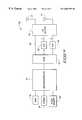
- the depicted communication system 10includes at least one electronic wireless remote communication device 12 and an interrogator 26 . Radio frequency communications can occur intermediate remote communication devices 12 and interrogator 26 for use in identification systems and product monitoring systems as exemplary applications.
- Devices 12include radio frequency identification devices (RFID) or remote intelligent communication (RIC) devices in the embodiments described herein. Exemplary devices 12 are disclosed in U.S. patent application Ser. No. 08/705,043, filed Aug. 29, 1996. Plural wireless remote communication devices 12 typically communicate with interrogator 26 although only one such device 12 is illustrated in FIG. 1 .
- RFIDradio frequency identification devices
- RICremote intelligent communication
- wireless remote communication device 12comprises a wireless identification device such as the MicroStamp (TM) integrated circuit available from Micron Communications, Inc., 3176 S. Denver Way, Boise, Id. 83705.
- TMMicroStamp
- Such a remote communication device 12can be referred to as a tag or card as illustrated and described below.
- multiple communication devices 12can be employed in communication system. 10 , there is typically no communication between multiple devices 12 . Instead, the multiple communication devices 12 communicate with interrogator 26 . Multiple communication devices 12 can be used in the same field of interrogator 26 (i.e., within the communications range of interrogator 26 ). Similarly, multiple interrogators 26 can be in proximity to one or more of devices 12 .
- Remote communication device 12is configured to interface with interrogator 26 using a wireless medium in one embodiment. More specifically, communications intermediate communication device 12 and interrogator 26 occur via an electromagnetic link, such as an RF link (e.g., at microwave frequencies) in the described embodiment. Interrogator 26 is configured to output forward link wireless communications 27 . Further, interrogator 26 is operable to receive reply or return link wireless communications 29 from devices 12 responsive to the outputting of forward link communication 27 .
- forward link communications and return link communicationscomprise wireless signals, such as radio frequency signals, in the described embodiment. Other forms of electromagnetic communication, such as infrared, acoustic, etc. are possible.
- Interrogator unit 26includes a plurality of antennas X 1 , R 1 , as well as transmitting and receiving circuitry, similar to that implemented in devices 12 .
- Antenna X 1comprises a transmit antenna and antenna R 1 comprises a receive antenna individually connected to interrogator 26 .
- interrogator 26transmits the interrogation command or forward link communication signal 27 via antenna X 1 .
- Communication device 12is operable to receive the incoming forward link signal. Upon receiving signal 27 , communication device 12 is operable to respond by communicating the responsive reply or return link communication signal 29 . Communications of system 10 are described in greater detail below.
- responsive signal 29is encoded with information that uniquely identifies, or labels the particular device 12 that is transmitting, so as to identify any object, animal, or person with which communication device 12 is associated.
- remote device 12is configured to output an identification signal within reply link communication 29 responsive to receiving forward link wireless communication 27 .
- Interrogator 26is configured to receive and recognize the identification signal within the return or reply link communication 29 .
- the identification signalcan be utilized to identify the particular transmitting communication device 12 .
- the depicted communication device 12includes a transponder 16 having a receiver and a transmitter as described below.
- Communication device 12further includes a power source 18 connected to transponder 16 to supply operational power to transponder 16 .
- transponder 16is in the form of an integrated circuit 19 .
- all of the circuitry of transponder 16is not necessarily all included in integrated circuit 19 .
- Power source 18is a thin film battery in the illustrated embodiment, however, in alternative embodiments, other forms of power sources can be employed. If the power source 18 is a battery, the battery can take any suitable form. Preferably, the battery type will be selected depending on weight, size, and life requirements for a particular application. In one embodiment, battery 18 is a thin profile button-type cell forming a small, thin energy cell more commonly utilized in watches and small electronic devices requiring a thin profile. A conventional button-type cell has a pair of electrodes, an anode formed by one face and a cathode formed by an opposite face. In an alternative embodiment, the battery comprises a series connected pair of button type cells.
- Communication device 12further includes at least one antenna connected to transponder 16 for wireless transmission and reception.
- communication device 12includes at least one receive antenna 44 connected to transponder 16 for radio frequency reception by transponder 16 , and at least one transmit antenna 46 connected to transponder 16 for radio frequency transmission by transponder 16 .
- the described receive antenna 44comprises a loop antenna and the transmit antenna 46 comprises a dipole antenna.
- FIG. 2shows but one example of a housing in the form of a miniature housing 11 encasing device 12 to define a tag which can be supported by an object (e.g., hung from an object, affixed to an object, etc.).
- an objecte.g., hung from an object, affixed to an object, etc.
- FIG. 3shows a housing in the form of a card 13 .
- Card 13preferably comprises plastic or other suitable material.
- Plastic card 13houses communication device 12 to define an employee identification badge including the communication device 12 .
- the front face of card 13has visual identification features such as an employee photograph or a fingerprint in addition to identifying text.
- the communication device 12can be included in any appropriate housing.
- Communication device 12is preferably of a small size that lends itself to applications employing small housings, such as cards, miniature tags, etc. Larger housings can also be employed.
- the communication device 12provided in any appropriate housing, can be supported from or attached to an object in any desired manner.
- FIG. 4is a high level circuit schematic of transponder 16 utilized in the devices of FIGS. 1-3.
- transponder 16is implemented within monolithic integrated circuit 19 .
- integrated circuit 19comprises a single die, having a size of 209 ⁇ 116 mils 2 , including a receiver 30 , transmitter 32 , microcontroller or microprocessor 34 , a wake up timer and logic circuit 36 , a clock recovery and data recovery circuit 38 , and a bias voltage and current generator 42 .
- Integrated circuit 19preferably comprises a small outline integrated circuit (SOIC) package.
- Receiver 30 and transmitter 32comprise wireless communication circuitry configured to communicate wireless signals.
- communication devices 12switch between a “sleep” mode of operation, and higher power modes to conserve energy and extend battery life during periods of time where no interrogation signal 27 is received by devices 12 , using the wake up timer and logic circuitry 36 .
- a spread spectrum processing circuit 40is included in transponder 16 .
- signals transmitted and received by interrogator 26 and signals transmitted and received by communication device 12are modulated spread spectrum signals.
- Many modulation techniquesminimize required transmission bandwidth.
- the spread spectrum modulation techniques employed in the illustrated embodimentrequire a transmission bandwidth that is up to several orders of magnitude greater than the minimum required signal bandwidth.
- spread spectrum modulation techniquesare bandwidth inefficient in single user applications, they are advantageous where there are multiple users, as is the case with the preferred radio frequency identification communication system 10 of the present invention.
- the spread spectrum modulation technique of the illustrated embodimentis advantageous because the interrogator signal can be distinguished from other signals (e.g., radar, microwave ovens, etc.) operating at the same frequency.
- the spread spectrum signals transmitted by communication device 12 and interrogator 26are pseudo random and have noise-like properties when compared with the digital command or reply.
- the illustrated embodimentemploys direct sequence spread spectrum (DSSS) modulation.
- DSSSdirect sequence spread spectrum
- interrogator 26sends out a command that is spread around a certain center frequency (e.g, 2.44 GHz). After the interrogator transmits the command, and is expecting a response, the interrogator switches to a continuous wave (CW) mode for backscatter communications. In the continuous wave mode, interrogator 26 does not transmit any information. Instead, the interrogator just transmits a radio frequency continuous wave signal. In the described embodiment, the continuous wave signal comprises a radio frequency 2.44 GHz carrier signal. In other words, the continuous wave signal transmitted by interrogator 26 is not modulated. After communication device 12 receives the forward link communication from interrogator 26 , communication device 12 processes the command.
- a certain center frequencye.g, 2.44 GHz
- device 12modulates the continuous wave signal providing a modulated continuous wave signal to communicate return link communication 29 responsive to reception of forward communication signal 27 .
- Communication device 12may modulate the continuous wave signal according to a subcarrier or modulation signal. Modulation by device 12 comprises selective reflection of the continuous wave signal.
- device 12alternately reflects or does not reflect the continuous wave signal from the interrogator to send its reply. For example, in the illustrated embodiment, two halves of a dipole antenna are either shorted together or isolated from each other to send a reply.
- communication device 12can communicate in an active mode.
- the modulated continuous wave signal communicated from device 12comprises a carrier component and plural side band components about the carrier component resulting from the modulation. More specifically, the modulated continuous wave signal output from device 12 includes a radio frequency continuous wave signal having a first frequency (2.44 GHz), also referred to as a carrier component, and a subcarrier modulation signal having a different frequency (e.g., 600 kHz) and which provides the side band components. In particular, the side band components are at +/ ⁇ 600 kHz of the carrier component.
- the carrier and side band componentsare illustrated in FIG. 11 and FIG. 12 .
- the clock for transponder 16is extracted from the incoming message itself by clock recovery and data recovery circuitry 38 .
- This clockis recovered from the incoming message, and used for timing for microcontroller 34 and all the other clock circuitry on the chip, and also for deriving the transmitter carrier or the subcarrier, depending on whether the transmitter is operating in active mode or backscatter mode.
- the clock recovery and data recovery circuit 38In addition to recovering a clock, the clock recovery and data recovery circuit 38 also performs data recovery on valid incoming signals.
- the valid spread spectrum incoming signalis passed through the spread spectrum processing circuit 40 , and the spread spectrum processing circuit 40 extracts the actual ones and zeros of data from the incoming signal. More particularly, the spread spectrum processing circuit 40 takes chips from the spread spectrum signal, and reduces individual thirty-one chip sections down to a bit of one or zero, which is passed to microcontroller 34 .
- Microcontroller 34includes a serial processor, or I/O facility that receives the bits from spread spectrum processing circuit 40 .
- the microcontroller 34performs further error correction. More particularly, a modified hamming code is employed, where each eight bits of data is accompanied by five check bits used by the microcontroller 34 for error correction.
- Microcontroller 34further includes a memory, and after performing the data correction, microcontroller 34 stores bytes of the data bits in memory. These bytes contain a command sent by the interrogator 26 . Microcontroller 34 is configured to respond to the command.
- Communications from interrogator 26i.e., forward link communications
- devices 12i.e., return link communications
- forward and reply communicationsindividually include a calibration period, preamble, and Barker or start code which are followed by actual data in the described embodiment.
- the incoming forward link message and outgoing replypreferably also include a check sum or redundancy code so that transponder 16 or interrogator 26 can confirm receipt of the entire message or reply.
- Communication devices 12typically include an identification sequence identifying the particular tag or device 12 sending the reply. Such implements the identification operations of communication system 10 .
- Return link datacan be Differential Phase Shift Key (DPSK) modulated onto the continuous wave signal using a square wave subcarrier with a frequency of approximately 600 kHz (e.g., 596.1 kHz in one embodiment).
- DPSKDifferential Phase Shift Key
- a data 0corresponds to one phase and data 1 corresponds to another, shifted 180 degrees from the first phase.
- the subcarrier or modulation signalis used to modulate antenna impedance of transponder 16 and generate the modulated continuous wave signal.
- a switch between the two halves of the dipole antennais opened and closed.
- the antennabecomes the electrical equivalent of a single half-wavelength antenna that reflects a portion of the power being transmitted by the interrogator.
- the switchis open, the antenna becomes the electrical equivalent of two quarter-wavelength antennas that reflect very little of the power transmitted by the interrogator.
- the dipole antennais a printed microstrip half wavelength dipole antenna.
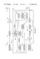
- interrogator 26includes a microcontroller 70 , a field programmable gate array (FPGA) 72 , and RF section 74 .
- microcontroller 70comprises a MC68340 microcontroller available from Motorola, Inc.
- FPGA 72comprises an XC4028 device available from Xilinx, Inc. Further details of components 70 , 72 , and 74 are described below.
- Microcontroller 70is configured to access an applications program for controlling the interrogator 26 and interpreting responses from devices 12 .
- the processor of microcontroller 70is configured to control communication operations with remote communication devices 12 during normal modes of operation.
- the applications programcan also include a library of radio frequency identification device applications or functions. These functions effect radio frequency communications between interrogator 26 and communication device 12 .
- RF section 74is configured to handle wireless (e.g., radio frequency) communications with remote communication devices 12 .
- DPSK modulation techniquescan be utilized for communications intermediate devices 12 and interrogator 26 .
- RF section 74can include downconversion circuitry for generating in-phase (I) and quadrature (Q) signals which contain the DPSK modulated subcarrier for application to FPGA 72 during return link communications.
- Plural antennasincluding a transmit antenna X 1 and a receive antenna R 1 are coupled with RF section 74 for wireless RF communications.
- Plural RF transmit (TX) ports and RF receive (RX) portsare coupled with RF section 74 in a preferred embodiment. Provision of plural TX ports and RX ports enables interrogator 26 to minimize the effects of multipath when communicating with plural remote communication devices 12 .
- Analog to digital converters 82 , 84provide received analog RF signals into a digital format for application to FPGA 72 .
- analog to digital converters 82 , 84are implemented intermediate FPGA 72 and RF section 74 for both in-phase (I) and quadrature (Q) communication lines.
- An additional connection 85is provided intermediate FPGA 72 and RF section 74 .
- Digital signals output from FPGA 72 via connection 85are converted to RF signals by RF section 74 .
- Connection 85can be utilized to transmit phase lock loop (PLL) information, antenna diversity selection information and other necessary communication information.
- PLLphase lock loop
- FPGA 72is configured to format communication packets received from microcontroller 70 into a proper format for application to RF section 74 for communication.
- FPGA 72is configured to demodulate return link communications received from remote communication devices 12 via RF section 74 .
- FPGA 72is configured in the described embodiment to perform I and Q combination operations during receive operations.
- the described FPGA 74further includes delay and multiplication circuitry to remove the subcarrier.
- FPGA 74can also include bit synchronization circuitry and lock detection circuitry. Data, clock and lock detection signals generated within FPGA 74 are applied to microcontroller 70 for processing in the described embodiment.
- Microcontroller 70is configured to control operations of interrogator 26 including outputting of forward link communications and receiving reply link communications.
- EPROM 78is configured to store original code and settings selected for the particular application of communication system 10 .
- Flash memory 80is configured to receive software code updates which may be forwarded to interrogator 26 .
- RAM device 76is configured to store data during operations of communication system 10 . Such data can include information regarding communications with associated remote communication devices 12 and status information of interrogator 26 during normal modes of operation.
- RF circuitry 74includes a transmit path 86 and a receive path 87 .
- RF section 74includes a transmitter 90 , coupler 91 and power amplifier 92 within transmit data path 86 .
- Receive path 87includes a receiver 95 comprising processing circuitry 96 and an adaptive canceler 97 in the depicted embodiment.
- Communication paths 86 , 87are coupled with respective antennas X 1 , R 1 .
- Transmit path 86is additionally coupled with FPGA 72 via connection 85 .
- Receive path 87is coupled with analog-to-digital converters 82 , 84 via the I, and Q connection lines.
- transmitter 90is configured to output a radio frequency wireless forward link communication 27 and a radio frequency wireless continuous wave signal using coupler 91 and antenna X 1 . Further, transmitter 90 is also configured to output a local continuous wave signal using coupler 91 . Transmitter 90 is preferably configured to simultaneously output the wireless continuous wave signal using antenna X 1 , and the local continuous wave signal using coupler 91 .
- the wireless continuous wave signal transmitted via antenna X 1 and the local continuous wave signal provided to receiver 95 via coupler 91have a common frequency (e.g., 2.44 GHz in the described embodiment).
- Receiver 95is operable to receive the return link communications 29 from at least one remote communication device 12 using antenna R 1 .
- adaptive canceler 97 of receiver 95is configured to receive the local continuous wave signal from coupler 91 . Provision of the local signal provides a coherent backscatter interrogator 26 including a coherent transmitter 90 and receiver 95 .
- receiver 95is operable to reduce the amplitude of the return link communication comprising the modulated continuous wave signal using the local continuous wave signal. More specifically, receiver 95 is configured to reduce the amplitude of the return link communications received by antenna R 1 at the common frequency of the continuous wave signals in the described embodiment.
- Adaptive canceler 97is configured to reduce the amplitude of return link communications 29 . More specifically, during backscatter communications, receive path 87 is susceptible to bleed through of the wireless continuous wave signal transmitted via antenna X 1 . More specifically, the wireless continuous wave signal communicated via transmit antenna X 1 can saturate the front end of receiver 95 . This leakage can desensitize receiver 95 and reduce the quality of wireless communications of interrogator 26 with remote communication devices 12 .
- Adaptive canceler 97utilizes the local continuous wave signal received from transmitter 90 and coupler 91 to reduce the amplitude of the return link communication received by antenna R 1 at the frequency of the wireless continuous wave signal transmitted via antenna X 1 .
- transmitter 90is configured to output local and wireless continuous wave signals using coupler 91 .
- the local continuous wave signalis applied to a variable attenuator 105 within adaptive canceler 97 .
- variable attenuator 105comprises a voltage controlled attenuator.
- Variable attenuator 105is configured to adjust the amplitude of the local continuous wave signal responsive to an external control signal discussed below.
- Variable attenuator 105outputs an amplitude adjusted local continuous wave signal.
- the amplitude adjusted local continuous wave signalis applied to a phase shifter 106 .
- Phase shifter 106preferably comprises a 360° phase shifter configured to provide an appropriate phase shift of the amplitude adjusted local continuous wave signal.
- Phase shifter 106outputs an amplitude and phase adjusted local continuous wave signal which is also referred to as the adjusted continuous wave signal.
- Phase shifter 106is controllable via an external control signal described below.
- the amplitude and phase adjusted local continuous wave signal output from phase shifter 106is supplied to a power divider 107 .
- Power divider 107operates to apply the signal to a detector 108 and coupler 109 .
- Detector 108is operable to measure the amplitude of the adjusted local signal and apply an output signal to an amplitude adjuster 110 .
- Coupler 114applies the received return link communication 29 to coupler 109 and an amplitude detector 115 .
- Detector 115is configured to measure the amplitude of the received return link communication 29 .
- Detectors 108 , 115individually comprise discrete components including diodes, resistors and capacitors. Detectors 108 , 115 are configured to measure the amplitude of the respective adjusted continuous wave signal and the modulated continuous wave signal.
- the measured amplitude valuesare applied to amplitude adjuster 110 which comprises a feedback amplifier configuration in the depicted embodiment.
- the illustrated analog implementation of amplitude adjuster 110is configured to drive variable attenuator 105 to equalize the amplitudes of the adjusted continuous wave signal and the modulated continuous wave signal.
- Amplitude adjuster 110is configured to compare the amplitudes of the adjusted continuous wave signal and the received return link communication comprising the modulated continuous wave signal. Thereafter, amplitude adjuster 110 is operable to output a control signal to variable attenuator 105 to match the amplitudes of the respective signals.
- Other configurations of amplitude adjuster 110are possible.
- coupler 109is configured to sum the adjusted continuous wave signal and the received modulated continuous wave signal to reduce the amplitude of the modulated continuous wave signal.
- the summed continuous wave signal or return link communicationis applied to a coupler 118 .
- Coupler 118is configured to apply the summed signal to low noise amplifier (LNA) 119 and amplitude detector 120 .
- Amplitude detector 120is configured to measure the amplitude of the summed signal and apply an output signal to a phase adjuster 121 .
- LNAlow noise amplifier
- Phase adjuster 121is controllable responsive to amplitude adjuster 110 . Once amplitude adjuster 110 and variable attenuator 105 have matched the amplitudes of the adjusted continuous wave signal and the received return link communication, amplitude adjuster indicates the match to phase adjuster 121 via a connection 122 . Thereafter, phase adjuster 121 operates to select an appropriate phase shift of the amplitude adjusted local continuous wave signal.
- phase adjuster 121is configured to search across 360° of possible phase adjustments to detect a phase adjustment of the local continuous wave signal which provides maximum reduction of amplitude of the received modulated continuous wave signal at the continuous wave signal frequency.
- adaptive canceler 97adjusts the phase of the local continuous wave signal following matching of amplitudes of the local continuous wave signal and the received modulated continuous wave signal as indicated via connection 122 .
- phase adjuster 121will apply an appropriate control signal to phase shifter 106 to implement the desired phase shift of approximately 150° to minimize the amplitude of the bleed through of the wireless continuous wave signal within the received return link communication.
- Phase adjuster 121is operable to continuously monitor the amplitude of the summed return link communication and provide appropriate adjustments using control signals applied to phase shifter 106 to minimize the amplitude of the continuous wave signal within the summed return link communication applied to LNA 119 .
- Amplitude detector 120includes discrete components comprising a diode, resistor and capacitor.
- Phase adjuster 121comprises an analog-to-digital converter 124 , processor 125 and digital-to-analog converter 126 .
- Processor 125can be configured to execute appropriate algorithms to implement sequential phase shifts of the local signal from 0° to 360°. The incremental step sizes can be adjusted. Therefore, processor 125 can compare the amplitudes of the summed return link communication signal responsive to various phase adjustments implemented by phase shifter 106 . Following selection of an appropriate phase shift, phase adjuster 121 can continue to monitor the amplitude of the summed return link communication and update the phase shift as necessary to maintain maximum reduction of the continuous wave signal within the return link communication during communications.
- the depicted configurations of detector 120 and phase adjuster 121are illustrative and other configurations can be utilized.
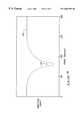
- the received return link communication applied to adaptive canceler 97 and the summed return link communication output from adaptive canceler 97are illustrated.
- the received return link communication comprising the modulated continuous wave signalis illustrated as signal 132 in FIG. 11 .
- the summed return link communicationis represented by signal 136 of FIG. 12 .
- Signal 132comprises a carrier component 133 and side band components 134 .
- carrier 133is centered at a frequency of 2.44 GHz and subcarrier side band components 134 are depicted at locations +/ ⁇ 600 kHz of the carrier component 133 .
- Signal 136similarly comprises a carrier component 137 and side band components 138 .
- Signal 136includes carrier component 137 at a frequency of 2.44 GHz and side band components 138 at locations +/ ⁇ 600 kHz of the carrier component 137 .
- the output summed return link communication signal 136has a carrier component 137 having a reduced amplitude compared with the carrier component 133 of the received return link communication signal 132 .
- the amplitude of side band components 138 of summed return link communication signal 136are maintained during the reduction of amplitude of the carrier component 137 as illustrated in FIG. 11 and FIG. 12 .
- carrier component 137 of signal 136is approximately 20 dBm less than carrier component 133 of received return link communication 132 . Such indicates the reduction of amplitude of the return link communication signal at the frequency of the wireless continuous wave signal (e.g., 2.44 GHz) utilizing adaptive canceler 97 .
- forward link communication 27is communicated using transmit antenna X 1 of interrogator 26 .
- return link communication 29corresponding to remote communication device 12 is communicated.
- Individual return link communications 29include a calibration period 140 followed by a preamble 141 and actual data 142 . Matching of amplitudes of the local continuous wave signal and the received return link communication and cycling through phases from 0 to 360° utilizing phase adjuster 121 and phase shifter 106 preferably occurs during calibration period 140 . The minimum level 130 within the summed return link communication signal is preferably determined during calibration period 140 .
- Preamble 141can be utilized to synchronize the processing circuitry 96 of receiver 95 with the actual return link communication 29 being received. Thereafter, data 142 communicated from remote communication device 12 is received. Adaptive canceler 97 is configured to make adjustments as necessary to the amplitude and phase of the local continuous signal during preamble period 141 and data period 142 to maintain maximum reduction of the continuous wave signal within the received return link communication 29 .
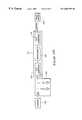
- FIG. 14illustrates a variable phase shifter 106 in accordance with one embodiment of the invention.
- Conventional phase shifters available in the marketplacecould be employed; however, these are extremely expensive.
- the phase shifter 106 illustrated in FIG. 14is an inexpensive alternative. Additionally, the phase shifter 106 provides phase shifts of anywhere from 0 to 360 degrees.
- the depicted phase shifter 106uses a commonly available part known as an IQ upconverter or IQ downconverter 201 .
- the IQ upconverter or IQ downconverter 201includes a first power divider 200 defining an input 210 and having two outputs 212 and 214 , a second power divider 208 defining an output 202 and having two inputs 204 , 206 , and two mixers 216 and 218 .
- first power divider 200comprises a ninety degree power divider and second power divider 208 comprises a zero degree power divider.
- Power divider 200receives an input signal having a phase angle from input 210 which is the amplitude adjusted local continuous wave signal received from variable attenuator 105 previously described.
- Power divider 200provides a ninety degree phase shift to the input signal to provide a first component and a second component in accordance with one embodiment of the invention.
- first and second components of the received signalmay be referred to as quadrature components.
- the first component from output 212is indicated as a cosine component (Cos( ⁇ t))
- the second component from output 214is indicated as a sine component (Sin( ⁇ t)).
- the signal components Cos( ⁇ t) and Sin( ⁇ t)have a sine/cosine relationship as they are shifted ninety degrees from each other.
- the quadrature signal components shifted ninety degrees apartare applied to respective mixers 216 , 218 .
- phase shifter 106further includes plural digital-to-analog (D/A) converters 224 , 226 , I, Q drivers 220 , 222 , and storage device 228 .
- Phase adjuster 121is coupled with storage device 228 .
- a second input 203 of phase shifter 106is provided intermediate phase adjuster 121 and storage device 228 .
- phase adjuster 121is configured to calculate a desired phase shift angle (also referred to herein as ⁇ ) and apply the phase shift angle to storage device 228 . More specifically, phase shifter 106 is configured to adjust the phase of the amplitude adjusted local continuous wave signal received from variable attenuator 105 responsive to control signals from phase adjuster 121 and corresponding to the phase shift angle. Appropriate control signals are generated within phase adjuster 121 to indicate the desired phase shift angle for shifting of the phase of the amplitude adjusted local continuous wave signal. In particular, the control signals correspond to the desired phase shift adjustment to provide the local minimum value 130 within the summed return link communication signal as previously described. The control signals identifying the proper phase adjustment are applied to phase shifter 106 .
- Storage device 228comprises a look-up table in an exemplary embodiment. Such a look-up table may be implemented within an EPROM in one embodiment. Storage device 228 can have one degree resolution, or other resolutions if desired. Storage device 228 is configured to store a plurality of sine values and cosine values, also referred to as I and Q digital values. Further, storage device 228 is configured to output one of the stored cosine values and one of the stored sine values to the respective D/A converters 224 , 226 responsive to and corresponding to the received phase shift angle determined by phase adjuster 121 .
- storage device 228outputs digital look-up table values of 0.707, 0.707 (i.e., cosine and sine of 45 degrees) which are provided to D/A converters 224 , 226 .
- Storage device 228is coupled with D/A converters 224 , 226 which in turn are coupled with respective I and Q drivers 220 , 222 .
- the cosine and sine digital values outputted from storage device 228are converted to analog voltages within D/A converters 224 , 226 .
- the corresponding analog voltage signals from D/A converters 224 , 226are applied to respective I and Q drivers 220 , 222 to implement the proper phase shift within the outputted signal to minimize bleed through.
- I driver 220is coupled to mixer 216 and Q driver 222 is coupled to mixer 218 as illustrated.
- Mixers 216 , 218are configured to scale the respective cosine and sine components of the input signal cos( ⁇ t), sin( ⁇ t) using the phase shift angle of phase adjuster 121 .
- mixers 216 , 218individually act as multipliers and multiply the cosine and sine components of the input signal by the respective cosine and sine values from storage device 228 as provided to I and Q drivers 220 , 222 .
- mixers 216 , 218multiply the cosine and sine components cos( ⁇ t), sin( ⁇ t) of the input signal by voltages outputted by the respective I driver 220 and the Q driver 222 and corresponding to the cosine value and sine value outputted from storage device 228 .
- phase shiftof anywhere between 0 degrees and 360 degrees can be obtained. Exemplary phase adjustments are described hereafter. Because the input signal components cos( ⁇ t) and sin( ⁇ t) are ninety degrees out of phase, if combined at the second power divider 200 comprising a zero degree power divider without use of multipliers 216 , 218 , the summed components represented as vectors would have the same value as the input signal plus a ninety degree phase shift of the input signal.
- the input signalhas a constant phase and an amplitude of 1. If the output signal is desired to have the exact same phase, then the I driver 220 is set to provide one volt to the mixer 216 and the Q driver 222 is set to provide zero volts to the mixer 218 . Thus, the signal applied to output 202 would be the same as the signal received from input 210 .
- the I driver 220would be set to provide zero volts to mixer 216 so there is no signal at output 204 , and the Q driver would be set to provide one volt to mixer 218 to produce a ninety degree phase shifted value at the output 202 .
- the I driver 220is set to provide 0.707 volts and the Q driver is set to provide 0.707 volts so by vector addition, the signal at the output 202 is shifted 45 degrees from the signal at the input 210 .
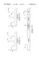
- FIG. 15illustrates the relationship between the I and Q signals applied to the mixers 216 , 218 , respectively.
- the relationshipis a sine/cosine relationship.
- Appropriate I and Q valuesmay be determined for any other desired degree phase shift (i.e., 0-360 degrees). For example, if a 45 degree phase shift is desired (i.e., ⁇ equals 45 degrees), I is at 0.707 (i.e., cosine ⁇ ) while Q is at 0.707 (i.e., sine ⁇ ) as determined within storage device 228 .
- cosine and sine valuesare provided to the respective I and Q drivers 220 , 222 .
- the signals outputted from mixers 216 , 218may be referred to as scaled quadrature cosine and sine components, respectively.
- the scaled quadrature component from mixer 216may be indicated as (Cos( ⁇ )Cos( ⁇ t)) and the scaled quadrature component from mixer 218 may be indicated as (Sin( ⁇ )Sin( ⁇ t)).
- the scaled quadrature componentsare applied to second power divider 208 .
- Power divider 208is configured to combine the first scaled quadrature component received from mixer 216 with the second scaled quadrature component received from mixer 218 to shift the phase angle of the local continuous wave signal by the phase shift angle received from phase adjuster 121 .
- Power divider 208is configured to add the scaled first and second quadrature components received from mixers 216 , 218 to implement phase shifting operations providing the adjusted continuous wave signal at output 202 .
- the adjusted continuous wave signal having a phase angle shifted by the desired phase shift angle ⁇is outputted from phase shifter 106 and may be applied via output 202 to power divider 107 and coupler 109 .
- coupler 109is configured to sum the adjusted continuous wave signal and the received modulated continuous wave signal. Such reduces-the amplitude of the modulated continuous wave signal at the frequency of the continuous wave to reduce bleed through of the carrier signal.
Landscapes
- Engineering & Computer Science (AREA)
- Computer Networks & Wireless Communication (AREA)
- Physics & Mathematics (AREA)
- General Physics & Mathematics (AREA)
- Radar, Positioning & Navigation (AREA)
- Remote Sensing (AREA)
- Signal Processing (AREA)
- Artificial Intelligence (AREA)
- Computer Vision & Pattern Recognition (AREA)
- Theoretical Computer Science (AREA)
- Near-Field Transmission Systems (AREA)
Abstract
Description
Claims (16)
Priority Applications (4)
| Application Number | Priority Date | Filing Date | Title |
|---|---|---|---|
| US09/265,082US6603391B1 (en) | 1999-03-09 | 1999-03-09 | Phase shifters, interrogators, methods of shifting a phase angle of a signal, and methods of operating an interrogator |
| US10/633,205US7091828B2 (en) | 1999-03-09 | 2003-08-01 | Interrogators, methods of operating a coherent interrogator, backscatter communication methods, interrogation methods, and signal processing methods |
| US11/502,999US7898390B2 (en) | 1999-03-09 | 2006-08-10 | Phase shifters, interrogators, methods of shifting a phase angle of a signal, and methods of operating an interrogator |
| US11/845,902US8174361B2 (en) | 1999-03-09 | 2007-08-28 | Phase shifters, interrogators, methods of shifting a phase angle of a signal, and methods of operating an interrogator |
Applications Claiming Priority (1)
| Application Number | Priority Date | Filing Date | Title |
|---|---|---|---|
| US09/265,082US6603391B1 (en) | 1999-03-09 | 1999-03-09 | Phase shifters, interrogators, methods of shifting a phase angle of a signal, and methods of operating an interrogator |
Related Child Applications (1)
| Application Number | Title | Priority Date | Filing Date |
|---|---|---|---|
| US10/633,205ContinuationUS7091828B2 (en) | 1999-03-09 | 2003-08-01 | Interrogators, methods of operating a coherent interrogator, backscatter communication methods, interrogation methods, and signal processing methods |
Publications (1)
| Publication Number | Publication Date |
|---|---|
| US6603391B1true US6603391B1 (en) | 2003-08-05 |
Family
ID=27623175
Family Applications (4)
| Application Number | Title | Priority Date | Filing Date |
|---|---|---|---|
| US09/265,082Expired - Fee RelatedUS6603391B1 (en) | 1999-03-09 | 1999-03-09 | Phase shifters, interrogators, methods of shifting a phase angle of a signal, and methods of operating an interrogator |
| US10/633,205Expired - Fee RelatedUS7091828B2 (en) | 1999-03-09 | 2003-08-01 | Interrogators, methods of operating a coherent interrogator, backscatter communication methods, interrogation methods, and signal processing methods |
| US11/502,999Expired - Fee RelatedUS7898390B2 (en) | 1999-03-09 | 2006-08-10 | Phase shifters, interrogators, methods of shifting a phase angle of a signal, and methods of operating an interrogator |
| US11/845,902Expired - Fee RelatedUS8174361B2 (en) | 1999-03-09 | 2007-08-28 | Phase shifters, interrogators, methods of shifting a phase angle of a signal, and methods of operating an interrogator |
Family Applications After (3)
| Application Number | Title | Priority Date | Filing Date |
|---|---|---|---|
| US10/633,205Expired - Fee RelatedUS7091828B2 (en) | 1999-03-09 | 2003-08-01 | Interrogators, methods of operating a coherent interrogator, backscatter communication methods, interrogation methods, and signal processing methods |
| US11/502,999Expired - Fee RelatedUS7898390B2 (en) | 1999-03-09 | 2006-08-10 | Phase shifters, interrogators, methods of shifting a phase angle of a signal, and methods of operating an interrogator |
| US11/845,902Expired - Fee RelatedUS8174361B2 (en) | 1999-03-09 | 2007-08-28 | Phase shifters, interrogators, methods of shifting a phase angle of a signal, and methods of operating an interrogator |
Country Status (1)
| Country | Link |
|---|---|
| US (4) | US6603391B1 (en) |
Cited By (62)
| Publication number | Priority date | Publication date | Assignee | Title |
|---|---|---|---|---|
| US20020090958A1 (en)* | 1999-03-09 | 2002-07-11 | Ovard David K. | Wireless communication systems, interrogators and methods of communication within a wireless communication system |
| US20040008800A1 (en)* | 2002-07-11 | 2004-01-15 | White Stanley A. | Methods and apparatus for delay free phase shifting in correcting PLL phase offset |
| US20040027240A1 (en)* | 1999-03-09 | 2004-02-12 | Roy Greeff | Interrogators, methods of operating a coherent interrogator, backscatter communication methods, interrogation methods, and signal processing methods |
| US20040127178A1 (en)* | 2002-12-30 | 2004-07-01 | Motorola, Inc. | Tunable duplexer |
| US20050121526A1 (en)* | 2003-12-09 | 2005-06-09 | Intelleflex Corporation | Battery activation circuit |
| US20050225435A1 (en)* | 2004-04-13 | 2005-10-13 | Impinj, Inc. | Adaptable bandwidth RFID tags |
| US20050225447A1 (en)* | 2004-04-13 | 2005-10-13 | Impinj, Inc., A Delaware Corporation | RFID readers transmitting preambles denoting communication parameters and RFID tags interpreting the same and methods |
| US20050237162A1 (en)* | 2004-04-13 | 2005-10-27 | Impinj, Inc., A Delaware Corporation | RFID readers transmitting preambles denoting data rate and methods |
| US20060183454A1 (en)* | 2005-02-14 | 2006-08-17 | Intelleflex Corporation | Adaptive coherent RFID reader carrier cancellation |
| US7095801B1 (en)* | 2001-03-30 | 2006-08-22 | Skyworks Solutions, Inc. | Phase adjustable polyphase filters |
| US20060252398A1 (en)* | 2005-05-09 | 2006-11-09 | Park Kyung H | Receiver of RFID reader for eliminating leakage signal |
| US20060255131A1 (en)* | 2005-05-11 | 2006-11-16 | Intelleflex Corporation | Smart tag activation |
| US20060261952A1 (en)* | 2004-04-13 | 2006-11-23 | Kavounas Gregory T | Adjusting RFID waveform shape in view of signal from an RFID tag |
| US20060261956A1 (en)* | 2004-04-13 | 2006-11-23 | Sundstrom Kurt E | Adjusting RFID waveform shape in view of signal from another reader |
| US20060267735A1 (en)* | 1999-03-09 | 2006-11-30 | Ovard David K | Wireless communication systems, interrogators and methods of communicating within a wireless communication system |
| US20060290438A1 (en)* | 2004-02-27 | 2006-12-28 | Micron Technology, Inc. | Microstrip line dielectric overlay |
| KR100706614B1 (en)* | 2005-09-29 | 2007-04-12 | 한국전자통신연구원 | Separate antenna for transmission and reception with high isolation |
| US20070126584A1 (en)* | 2004-04-13 | 2007-06-07 | Impimj, Inc. | Adaptable Detection Threshold for RFID Tags and Chips |
| US20070206704A1 (en)* | 2006-03-03 | 2007-09-06 | Applied Wireless Identification Group, Inc. | RFID reader with adaptive carrier cancellation |
| US20080303673A1 (en)* | 2007-06-08 | 2008-12-11 | Checkpoint Systems, Inc. | Dynamic eas detection system and method |
| US20090068957A1 (en)* | 2007-09-07 | 2009-03-12 | Koo Ji-Hun | Rfid reader compensating leakage signal and compensating method thereof |
| US20090224887A1 (en)* | 2008-03-10 | 2009-09-10 | Arash Sadeghfam | Adjustable circuit and rfid reader device |
| US20090261976A1 (en)* | 2007-06-08 | 2009-10-22 | Checkpoint Systems, Inc. | Phase coupler for rotating fields |
| US20100176927A1 (en)* | 2006-01-30 | 2010-07-15 | Voyantic Oy | Device and Method for Analysing Radio-Frequency Systems |
| US7830262B1 (en) | 2006-04-25 | 2010-11-09 | Impinj, Inc. | Adjusting communication parameters while inventorying RFID tags |
| US7959769B2 (en) | 2004-12-08 | 2011-06-14 | Infinite Power Solutions, Inc. | Deposition of LiCoO2 |
| US7993773B2 (en) | 2002-08-09 | 2011-08-09 | Infinite Power Solutions, Inc. | Electrochemical apparatus with barrier layer protected substrate |
| US8021778B2 (en) | 2002-08-09 | 2011-09-20 | Infinite Power Solutions, Inc. | Electrochemical apparatus with barrier layer protected substrate |
| USRE42751E1 (en) | 1998-09-03 | 2011-09-27 | Round Rock Research, Llc | Communication system, interrogators and communication methods |
| US8062708B2 (en) | 2006-09-29 | 2011-11-22 | Infinite Power Solutions, Inc. | Masking of and material constraint for depositing battery layers on flexible substrates |
| US8169312B2 (en) | 2009-01-09 | 2012-05-01 | Sirit Inc. | Determining speeds of radio frequency tags |
| US8197781B2 (en) | 2006-11-07 | 2012-06-12 | Infinite Power Solutions, Inc. | Sputtering target of Li3PO4 and method for producing same |
| US8226003B2 (en) | 2006-04-27 | 2012-07-24 | Sirit Inc. | Adjusting parameters associated with leakage signals |
| US8236443B2 (en) | 2002-08-09 | 2012-08-07 | Infinite Power Solutions, Inc. | Metal film encapsulation |
| US8248211B2 (en) | 2005-07-20 | 2012-08-21 | Intelleflex Corporation | Selective RF device activation |
| US8248212B2 (en) | 2007-05-24 | 2012-08-21 | Sirit Inc. | Pipelining processes in a RF reader |
| US8260203B2 (en) | 2008-09-12 | 2012-09-04 | Infinite Power Solutions, Inc. | Energy device with integral conductive surface for data communication via electromagnetic energy and method thereof |
| US8268488B2 (en) | 2007-12-21 | 2012-09-18 | Infinite Power Solutions, Inc. | Thin film electrolyte for thin film batteries |
| US8350519B2 (en) | 2008-04-02 | 2013-01-08 | Infinite Power Solutions, Inc | Passive over/under voltage control and protection for energy storage devices associated with energy harvesting |
| US8394522B2 (en) | 2002-08-09 | 2013-03-12 | Infinite Power Solutions, Inc. | Robust metal film encapsulation |
| US8404376B2 (en) | 2002-08-09 | 2013-03-26 | Infinite Power Solutions, Inc. | Metal film encapsulation |
| US8410905B2 (en) | 2007-07-10 | 2013-04-02 | Samsung Electronics Co., Ltd. | RFID reader cancelling leakage signal |
| US8416079B2 (en) | 2009-06-02 | 2013-04-09 | 3M Innovative Properties Company | Switching radio frequency identification (RFID) tags |
| US8427316B2 (en) | 2008-03-20 | 2013-04-23 | 3M Innovative Properties Company | Detecting tampered with radio frequency identification tags |
| US8431264B2 (en) | 2002-08-09 | 2013-04-30 | Infinite Power Solutions, Inc. | Hybrid thin-film battery |
| US8445130B2 (en) | 2002-08-09 | 2013-05-21 | Infinite Power Solutions, Inc. | Hybrid thin-film battery |
| US8446256B2 (en) | 2008-05-19 | 2013-05-21 | Sirit Technologies Inc. | Multiplexing radio frequency signals |
| US8508193B2 (en) | 2008-10-08 | 2013-08-13 | Infinite Power Solutions, Inc. | Environmentally-powered wireless sensor module |
| US8518581B2 (en) | 2008-01-11 | 2013-08-27 | Inifinite Power Solutions, Inc. | Thin film encapsulation for thin film batteries and other devices |
| US8548098B2 (en) | 2005-12-15 | 2013-10-01 | Intelleflex Corporation | Clock-free activation circuit |
| US8599572B2 (en) | 2009-09-01 | 2013-12-03 | Infinite Power Solutions, Inc. | Printed circuit board with integrated thin film battery |
| US8636876B2 (en) | 2004-12-08 | 2014-01-28 | R. Ernest Demaray | Deposition of LiCoO2 |
| US8728285B2 (en) | 2003-05-23 | 2014-05-20 | Demaray, Llc | Transparent conductive oxides |
| US8906523B2 (en) | 2008-08-11 | 2014-12-09 | Infinite Power Solutions, Inc. | Energy device with integral collector surface for electromagnetic energy harvesting and method thereof |
| US20150063430A1 (en)* | 2013-09-03 | 2015-03-05 | Favepc Inc. | Transceiver |
| US9334557B2 (en) | 2007-12-21 | 2016-05-10 | Sapurast Research Llc | Method for sputter targets for electrolyte films |
| US20160302384A1 (en)* | 2005-12-16 | 2016-10-20 | Cambridge Resonant Technologies Ltd. | Rfid reader |
| US9634296B2 (en) | 2002-08-09 | 2017-04-25 | Sapurast Research Llc | Thin film battery on an integrated circuit or circuit board and method thereof |
| US10062025B2 (en) | 2012-03-09 | 2018-08-28 | Neology, Inc. | Switchable RFID tag |
| EP3418939A1 (en)* | 2017-06-21 | 2018-12-26 | Kapsch TrafficCom AG | Method and rfid reader for obtaining a backscatter modulated receive signal |
| US10680277B2 (en) | 2010-06-07 | 2020-06-09 | Sapurast Research Llc | Rechargeable, high-density electrochemical device |
| US10840859B2 (en)* | 2016-06-24 | 2020-11-17 | Tokyo Keiki Inc. | Amplification apparatus |
Families Citing this family (13)
| Publication number | Priority date | Publication date | Assignee | Title |
|---|---|---|---|---|
| US20050141648A1 (en)* | 2003-12-24 | 2005-06-30 | Microchip Technology Incorporated | Time signal peripheral |
| NL1026338C2 (en)* | 2004-06-04 | 2005-12-06 | Nedap Nv | System for detection, location and identification according to the FM-CW principle. |
| EP1630713B1 (en)* | 2004-08-24 | 2020-05-20 | Sony Deutschland GmbH | Backscatter interrogator reception method and interrogator for a modulated backscatter system |
| SE0402571L (en)* | 2004-10-22 | 2005-09-27 | Cpum | RFID encoding |
| US20060208897A1 (en)* | 2005-03-04 | 2006-09-21 | Chiu Lihu M | Capacitive RFID tag encoder |
| NL1029590C2 (en)* | 2005-07-22 | 2007-01-23 | Nedap Nv | Radio frequency positioning system for animals, uses tag with antenna impedance modulated by signal from subcarrier wave generator |
| KR100746747B1 (en)* | 2006-02-06 | 2007-08-06 | 삼성전자주식회사 | Rfid reader |
| US8964498B2 (en)* | 2011-11-15 | 2015-02-24 | Marvell World Trade Ltd. | Systems and methods for reducing peak power consumption in a solid state drive controller |
| US9928721B2 (en) | 2013-09-24 | 2018-03-27 | Intermec Ip Corp. | Systems, methods, and apparatus to permit communication between passive wireless transponders |
| KR102447804B1 (en)* | 2017-09-05 | 2022-09-27 | 삼성전자주식회사 | Electronic device comprising a wireless communication system for processing a transmitted signal or a received signal |
| WO2019158196A1 (en)* | 2018-02-14 | 2019-08-22 | Telefonaktiebolaget Lm Ericsson (Publ) | Technique for backscattering transmission |
| WO2024121073A2 (en)* | 2022-12-05 | 2024-06-13 | Sony Group Corporation | Systems, methods and communications devices |
| JP2025024983A (en)* | 2023-08-08 | 2025-02-21 | セイコーエプソン株式会社 | Responder and positioning system |
Citations (6)
| Publication number | Priority date | Publication date | Assignee | Title |
|---|---|---|---|---|
| US4075632A (en) | 1974-08-27 | 1978-02-21 | The United States Of America As Represented By The United States Department Of Energy | Interrogation, and detection system |
| US4926182A (en) | 1986-05-30 | 1990-05-15 | Sharp Kabushiki Kaisha | Microwave data transmission apparatus |
| US5617060A (en) | 1994-04-28 | 1997-04-01 | Qualcomm Incorporated | Method and apparatus for automatic gain control and DC offset cancellation in quadrature receiver |
| US5621412A (en) | 1994-04-26 | 1997-04-15 | Texas Instruments Incorporated | Multi-stage transponder wake-up, method and structure |
| US5649296A (en) | 1995-06-19 | 1997-07-15 | Lucent Technologies Inc. | Full duplex modulated backscatter system |
| US6130602A (en) | 1996-05-13 | 2000-10-10 | Micron Technology, Inc. | Radio frequency data communications device |
Family Cites Families (71)
| Publication number | Priority date | Publication date | Assignee | Title |
|---|---|---|---|---|
| US5355A (en)* | 1847-11-06 | Washing-machine | ||
| US3195073A (en)* | 1961-07-26 | 1965-07-13 | Texas Instruments Inc | Single-sideband suppressed carrier signal generator |
| US3568197A (en)* | 1969-12-05 | 1971-03-02 | Nasa | Antenna array phase quadrature tracking system |
| US3733602A (en) | 1971-05-20 | 1973-05-15 | Motorola Inc | Microwave intrusion detecting system and apparatus |
| US3848191A (en) | 1972-07-07 | 1974-11-12 | Rca Corp | Asynchronous pulse receiver |
| US3914762A (en)* | 1973-12-27 | 1975-10-21 | Rca Corp | Electronic identification system |
| GB1500289A (en)* | 1974-06-03 | 1978-02-08 | Rca Corp | Homodyne communication system |
| GB1579299A (en)* | 1976-03-12 | 1980-11-19 | Nippon Paint Co Ltd | Resinous particles for coating composition |
| US4149121A (en)* | 1977-06-23 | 1979-04-10 | Ncr Corporation | Four phase to two phase correlator |
| US4364043A (en) | 1979-05-30 | 1982-12-14 | The University Of Adelaide | Efficient object identification system |
| JPS56132828A (en) | 1980-03-24 | 1981-10-17 | Nippon Telegr & Teleph Corp <Ntt> | Space diversity receiving device |
| IT1142442B (en)* | 1981-05-11 | 1986-10-08 | Selenia Ind Elettroniche | ADAPTIVE POLARIZATION RECEIVER FOR THE CANCELLATION OF INTENTIONAL DISORDERS IN A RADAR SYSTEM |
| US4385043A (en)* | 1981-07-10 | 1983-05-24 | The United States Of America As Represented By The Administrator Of The National Aeronautics And Space Administration | Method of carbonizing polyacrylonitrile fibers |
| US4384043A (en)* | 1981-09-02 | 1983-05-17 | American Cyanamid Company | Process for producing the antibiotic nosiheptide |
| US4725841A (en)* | 1983-06-30 | 1988-02-16 | X-Cyte, Inc. | System for interrogating a passive transponder carrying phase-encoded information |
| US4647931A (en)* | 1984-11-29 | 1987-03-03 | Rca Corporation | Dual frequency identification system |
| JPS62264778A (en) | 1986-05-12 | 1987-11-17 | Toshiba Corp | Agc circuit |
| US4799062A (en) | 1987-04-27 | 1989-01-17 | Axonn Corporation | Radio position determination method and apparatus |
| US5345504A (en) | 1988-03-10 | 1994-09-06 | Scientific-Atlanta, Inc. | Differential compensation control for off-premises CATV system |
| GB2223908A (en) | 1988-10-14 | 1990-04-18 | Philips Electronic Associated | Continuously transmitting and receiving radar |
| GB2226204A (en) | 1988-12-07 | 1990-06-20 | Philips Electronic Associated | Continuously transmitting and receiving radar |
| US5260707A (en)* | 1988-12-22 | 1993-11-09 | Hughes Aircraft Company | Phase coherent interference signal suppression system and method |
| US5657317A (en) | 1990-01-18 | 1997-08-12 | Norand Corporation | Hierarchical communication system using premises, peripheral and vehicular local area networking |
| US5305008A (en)* | 1991-08-12 | 1994-04-19 | Integrated Silicon Design Pty. Ltd. | Transponder system |
| US5134630A (en)* | 1989-04-12 | 1992-07-28 | National Research Development Corporation | Method and apparatus for transparent tone-in-band transmitter, receiver and system processing |
| US5640151A (en) | 1990-06-15 | 1997-06-17 | Texas Instruments Incorporated | Communication system for communicating with tags |
| US5231273A (en) | 1991-04-09 | 1993-07-27 | Comtec Industries | Inventory management system |
| US5365516A (en) | 1991-08-16 | 1994-11-15 | Pinpoint Communications, Inc. | Communication system and method for determining the location of a transponder unit |
| US5369793A (en)* | 1991-12-12 | 1994-11-29 | Raytheon Company | RF receiver adapted to process received RF pulses and reject RF continuous wave signals |
| US5349355A (en) | 1993-01-21 | 1994-09-20 | The United States Of America As Represented By The Secretary Of The Navy | Credential tracking system |
| JPH06260866A (en) | 1993-03-04 | 1994-09-16 | Mitsubishi Electric Corp | Automatic output power control circuit device |
| JPH06261010A (en)* | 1993-03-04 | 1994-09-16 | Fujitsu Ltd | Fading simulation method and fading simulator |
| US5477215A (en) | 1993-08-02 | 1995-12-19 | At&T Corp. | Arrangement for simultaneously interrogating a plurality of portable radio frequency communication devices |
| US5610940A (en)* | 1994-09-09 | 1997-03-11 | Omnipoint Corporation | Method and apparatus for noncoherent reception and correlation of a continous phase modulated signal |
| US5584065A (en)* | 1994-10-13 | 1996-12-10 | American Nucleonics Corporation | Interference cancellation system employing an I/Q quadrature rotator |
| US5691978A (en)* | 1995-04-07 | 1997-11-25 | Signal Science, Inc. | Self-cancelling full-duplex RF communication system |
| ZA965340B (en) | 1995-06-30 | 1997-01-27 | Interdigital Tech Corp | Code division multiple access (cdma) communication system |
| US5624412A (en)* | 1995-07-11 | 1997-04-29 | Weekley; Jack L. | I-V Caddy |
| US5940006A (en) | 1995-12-12 | 1999-08-17 | Lucent Technologies Inc. | Enhanced uplink modulated backscatter system |
| US6058374A (en) | 1996-06-20 | 2000-05-02 | Northrop Grumman Corporation | Inventorying method and system for monitoring items using tags |
| US5926747A (en) | 1996-09-05 | 1999-07-20 | Airnet Communications Corp. | Method and apparatus for dynamically optimizing the forward-link transmit power of a broadband multi-carrier radio signal |
| CA2268951A1 (en) | 1996-10-17 | 1998-04-23 | Pinpoint Corporation | Article tracking system |
| US6353406B1 (en) | 1996-10-17 | 2002-03-05 | R.F. Technologies, Inc. | Dual mode tracking system |
| US6107910A (en)* | 1996-11-29 | 2000-08-22 | X-Cyte, Inc. | Dual mode transmitter/receiver and decoder for RF transponder tags |
| US5842118A (en) | 1996-12-18 | 1998-11-24 | Micron Communications, Inc. | Communication system including diversity antenna queuing |
| US6289209B1 (en) | 1996-12-18 | 2001-09-11 | Micron Technology, Inc. | Wireless communication system, radio frequency communications system, wireless communications method, radio frequency communications method |
| US5970388A (en) | 1996-12-26 | 1999-10-19 | Will; Craig A. | Wireless system for indicating an incoming telephone call and controlling its transfer |
| US6084530A (en) | 1996-12-30 | 2000-07-04 | Lucent Technologies Inc. | Modulated backscatter sensor system |
| US5952922A (en)* | 1996-12-31 | 1999-09-14 | Lucent Technologies Inc. | In-building modulated backscatter system |
| US6456668B1 (en) | 1996-12-31 | 2002-09-24 | Lucent Technologies Inc. | QPSK modulated backscatter system |
| US5784686A (en)* | 1996-12-31 | 1998-07-21 | Lucent Technologies Inc. | IQ combiner technology in modulated backscatter system |
| US6046683A (en)* | 1996-12-31 | 2000-04-04 | Lucent Technologies Inc. | Modulated backscatter location system |
| US5920287A (en)* | 1997-01-21 | 1999-07-06 | Widata Corporation | Radio location system for precisely tracking objects by RF transceiver tags which randomly and repetitively emit wideband identification signals |
| US5914671A (en)* | 1997-02-27 | 1999-06-22 | Micron Communications, Inc. | System and method for locating individuals and equipment, airline reservation system, communication system |
| US6064320A (en) | 1997-04-04 | 2000-05-16 | Texas Instruments Incorporated | Automatic vehicle identification system capable of vehicle lane discrimination |
| US6148048A (en) | 1997-09-26 | 2000-11-14 | Cirrus Logic, Inc. | Receive path implementation for an intermediate frequency transceiver |
| US5983082A (en)* | 1997-10-31 | 1999-11-09 | Motorola, Inc. | Phase quadrature signal generator having a variable phase shift network |
| US6353729B1 (en) | 1997-11-14 | 2002-03-05 | Nortel Networks Limited | Using an RF repeater in CDMA applications to combat interference caused by a non-collocated radio |
| JP3941082B2 (en)* | 1998-01-28 | 2007-07-04 | 株式会社安川電機 | Magnetic detector |
| US6122329A (en)* | 1998-02-06 | 2000-09-19 | Intermec Ip Corp. | Radio frequency identification interrogator signal processing system for reading moving transponders |
| US6313737B1 (en) | 1998-06-23 | 2001-11-06 | Marconi Commerce Systems Inc. | Centralized transponder arbitration |
| US6192222B1 (en)* | 1998-09-03 | 2001-02-20 | Micron Technology, Inc. | Backscatter communication systems, interrogators, methods of communicating in a backscatter system, and backscatter communication methods |
| US6324387B1 (en) | 1998-12-29 | 2001-11-27 | Philips Electronics N.A. Corp. | LNA control-circuit for receive closed loop automatic gain control |
| US6356764B1 (en) | 1999-03-09 | 2002-03-12 | Micron Technology, Inc. | Wireless communication systems, interrogators and methods of communicating within a wireless communication system |
| US6603391B1 (en)* | 1999-03-09 | 2003-08-05 | Micron Technology, Inc. | Phase shifters, interrogators, methods of shifting a phase angle of a signal, and methods of operating an interrogator |
| US7592898B1 (en) | 1999-03-09 | 2009-09-22 | Keystone Technology Solutions, Llc | Wireless communication systems, interrogators and methods of communicating within a wireless communication system |
| US6356230B1 (en) | 1999-08-20 | 2002-03-12 | Micron Technology, Inc. | Interrogators, wireless communication systems, methods of operating an interrogator, methods of monitoring movement of a radio frequency identification device, methods of monitoring movement of a remote communication device and movement monitoring methods |
| US6721549B2 (en) | 1999-12-29 | 2004-04-13 | Samsung Electronics Co., Ltd. | Low-noise amplifier for a mobile communication terminal |
| US7023341B2 (en) | 2003-02-03 | 2006-04-04 | Ingrid, Inc. | RFID reader for a security network |
| US6903656B1 (en) | 2003-05-27 | 2005-06-07 | Applied Wireless Identifications Group, Inc. | RFID reader with multiple antenna selection and automated antenna matching |
| US7369811B2 (en) | 2004-04-30 | 2008-05-06 | Wj Communications, Inc. | System and method for sensitivity optimization of RF receiver using adaptive nulling |
- 1999
- 1999-03-09USUS09/265,082patent/US6603391B1/ennot_activeExpired - Fee Related
- 2003
- 2003-08-01USUS10/633,205patent/US7091828B2/ennot_activeExpired - Fee Related
- 2006
- 2006-08-10USUS11/502,999patent/US7898390B2/ennot_activeExpired - Fee Related
- 2007
- 2007-08-28USUS11/845,902patent/US8174361B2/ennot_activeExpired - Fee Related
Patent Citations (6)
| Publication number | Priority date | Publication date | Assignee | Title |
|---|---|---|---|---|
| US4075632A (en) | 1974-08-27 | 1978-02-21 | The United States Of America As Represented By The United States Department Of Energy | Interrogation, and detection system |
| US4926182A (en) | 1986-05-30 | 1990-05-15 | Sharp Kabushiki Kaisha | Microwave data transmission apparatus |
| US5621412A (en) | 1994-04-26 | 1997-04-15 | Texas Instruments Incorporated | Multi-stage transponder wake-up, method and structure |
| US5617060A (en) | 1994-04-28 | 1997-04-01 | Qualcomm Incorporated | Method and apparatus for automatic gain control and DC offset cancellation in quadrature receiver |
| US5649296A (en) | 1995-06-19 | 1997-07-15 | Lucent Technologies Inc. | Full duplex modulated backscatter system |
| US6130602A (en) | 1996-05-13 | 2000-10-10 | Micron Technology, Inc. | Radio frequency data communications device |
Cited By (112)
| Publication number | Priority date | Publication date | Assignee | Title |
|---|---|---|---|---|
| USRE43242E1 (en)* | 1998-09-03 | 2012-03-13 | Round Rock Research, Llc | Communication system, interrogators and communication methods |
| USRE42751E1 (en) | 1998-09-03 | 2011-09-27 | Round Rock Research, Llc | Communication system, interrogators and communication methods |
| US20060267735A1 (en)* | 1999-03-09 | 2006-11-30 | Ovard David K | Wireless communication systems, interrogators and methods of communicating within a wireless communication system |
| US20070290806A1 (en)* | 1999-03-09 | 2007-12-20 | Roy Greeff | Phase Shifters, Interrogators, Methods Of Shifting A Phase Angle Of A Signal, And Methods Of Operating An Interrogator |
| US7898390B2 (en) | 1999-03-09 | 2011-03-01 | Round Rock Research, Llc | Phase shifters, interrogators, methods of shifting a phase angle of a signal, and methods of operating an interrogator |
| US7969284B2 (en) | 1999-03-09 | 2011-06-28 | Round Rock Research, Llc | Wireless communication systems, interrogators and methods of communicating within a wireless communication system |
| US7982586B2 (en) | 1999-03-09 | 2011-07-19 | Round Rock Research, Llc | Wireless communication systems, interrogators and methods of communicating within a wireless communication system |
| US20020090958A1 (en)* | 1999-03-09 | 2002-07-11 | Ovard David K. | Wireless communication systems, interrogators and methods of communication within a wireless communication system |
| US7091828B2 (en)* | 1999-03-09 | 2006-08-15 | Micron Technology, Inc. | Interrogators, methods of operating a coherent interrogator, backscatter communication methods, interrogation methods, and signal processing methods |
| US20080001754A1 (en)* | 1999-03-09 | 2008-01-03 | Ovard David K | Wireless Communication Systems, Interrogators and Methods of Communicating Within a Wireless Communication System |
| US7592898B1 (en) | 1999-03-09 | 2009-09-22 | Keystone Technology Solutions, Llc | Wireless communication systems, interrogators and methods of communicating within a wireless communication system |
| US20060279407A1 (en)* | 1999-03-09 | 2006-12-14 | Roy Greeff | Phase shifters, interrogators, methods of shifting a phase angle of a signal, and methods of operating an interrogator |
| US20070290813A1 (en)* | 1999-03-09 | 2007-12-20 | Ovard David K | Wireless Communication Systems, Interrogators and Methods of Communicating Within a Wireless Communication System |
| US8174361B2 (en) | 1999-03-09 | 2012-05-08 | Round Rock Research, Llc | Phase shifters, interrogators, methods of shifting a phase angle of a signal, and methods of operating an interrogator |
| US20040027240A1 (en)* | 1999-03-09 | 2004-02-12 | Roy Greeff | Interrogators, methods of operating a coherent interrogator, backscatter communication methods, interrogation methods, and signal processing methods |
| US8351968B2 (en) | 1999-03-09 | 2013-01-08 | Round Rock Research, Llc | Wireless communication systems, interrogators and methods of communication within a wireless communication system |
| US7095801B1 (en)* | 2001-03-30 | 2006-08-22 | Skyworks Solutions, Inc. | Phase adjustable polyphase filters |
| US7224759B2 (en)* | 2002-07-11 | 2007-05-29 | Honeywell International Inc. | Methods and apparatus for delay free phase shifting in correcting PLL phase offset |
| US20040008800A1 (en)* | 2002-07-11 | 2004-01-15 | White Stanley A. | Methods and apparatus for delay free phase shifting in correcting PLL phase offset |
| US8236443B2 (en) | 2002-08-09 | 2012-08-07 | Infinite Power Solutions, Inc. | Metal film encapsulation |
| US8445130B2 (en) | 2002-08-09 | 2013-05-21 | Infinite Power Solutions, Inc. | Hybrid thin-film battery |
| US9793523B2 (en) | 2002-08-09 | 2017-10-17 | Sapurast Research Llc | Electrochemical apparatus with barrier layer protected substrate |
| US8394522B2 (en) | 2002-08-09 | 2013-03-12 | Infinite Power Solutions, Inc. | Robust metal film encapsulation |
| US8404376B2 (en) | 2002-08-09 | 2013-03-26 | Infinite Power Solutions, Inc. | Metal film encapsulation |
| US8021778B2 (en) | 2002-08-09 | 2011-09-20 | Infinite Power Solutions, Inc. | Electrochemical apparatus with barrier layer protected substrate |
| US8431264B2 (en) | 2002-08-09 | 2013-04-30 | Infinite Power Solutions, Inc. | Hybrid thin-film battery |
| US9634296B2 (en) | 2002-08-09 | 2017-04-25 | Sapurast Research Llc | Thin film battery on an integrated circuit or circuit board and method thereof |
| US8535396B2 (en) | 2002-08-09 | 2013-09-17 | Infinite Power Solutions, Inc. | Electrochemical apparatus with barrier layer protected substrate |
| US7993773B2 (en) | 2002-08-09 | 2011-08-09 | Infinite Power Solutions, Inc. | Electrochemical apparatus with barrier layer protected substrate |
| US20040127178A1 (en)* | 2002-12-30 | 2004-07-01 | Motorola, Inc. | Tunable duplexer |
| US7212789B2 (en)* | 2002-12-30 | 2007-05-01 | Motorola, Inc. | Tunable duplexer |
| US8728285B2 (en) | 2003-05-23 | 2014-05-20 | Demaray, Llc | Transparent conductive oxides |
| US20050121526A1 (en)* | 2003-12-09 | 2005-06-09 | Intelleflex Corporation | Battery activation circuit |
| US7612652B2 (en) | 2003-12-09 | 2009-11-03 | Intelleflex Corporation | Battery activation circuit |
| US7432774B2 (en) | 2004-02-27 | 2008-10-07 | Micron Technology, Inc. | Microstrip line dielectric overlay |
| US9214713B2 (en) | 2004-02-27 | 2015-12-15 | Micron Technology, Inc. | Method of fabricating a microstrip line dielectric overlay |
| US7436267B2 (en) | 2004-02-27 | 2008-10-14 | Micron Technology, Inc. | Microstrip line dielectric overlay |
| US20060290438A1 (en)* | 2004-02-27 | 2006-12-28 | Micron Technology, Inc. | Microstrip line dielectric overlay |
| US20090025204A1 (en)* | 2004-02-27 | 2009-01-29 | Micron Technology, Inc. | Microstrip line dielectric overlay |
| US8258955B1 (en) | 2004-04-13 | 2012-09-04 | Impinj, Inc. | Adaptable detection threshold for RFID tags and chips |
| US20050237162A1 (en)* | 2004-04-13 | 2005-10-27 | Impinj, Inc., A Delaware Corporation | RFID readers transmitting preambles denoting data rate and methods |
| US20070126584A1 (en)* | 2004-04-13 | 2007-06-07 | Impimj, Inc. | Adaptable Detection Threshold for RFID Tags and Chips |
| US20050225447A1 (en)* | 2004-04-13 | 2005-10-13 | Impinj, Inc., A Delaware Corporation | RFID readers transmitting preambles denoting communication parameters and RFID tags interpreting the same and methods |
| US7973643B2 (en) | 2004-04-13 | 2011-07-05 | Impinj, Inc. | RFID readers transmitting preambles denoting data rate and methods |
| US7417548B2 (en)* | 2004-04-13 | 2008-08-26 | Impinj, Inc. | Adjusting RFID waveform shape in view of signal from an RFID tag |
| US20050225435A1 (en)* | 2004-04-13 | 2005-10-13 | Impinj, Inc. | Adaptable bandwidth RFID tags |
| US7501953B2 (en) | 2004-04-13 | 2009-03-10 | Impinj Inc | RFID readers transmitting preambles denoting communication parameters and RFID tags interpreting the same and methods |
| US20060261952A1 (en)* | 2004-04-13 | 2006-11-23 | Kavounas Gregory T | Adjusting RFID waveform shape in view of signal from an RFID tag |
| US20060261956A1 (en)* | 2004-04-13 | 2006-11-23 | Sundstrom Kurt E | Adjusting RFID waveform shape in view of signal from another reader |
| US7917088B2 (en) | 2004-04-13 | 2011-03-29 | Impinj, Inc. | Adaptable detection threshold for RFID tags and chips |
| US7183926B2 (en) | 2004-04-13 | 2007-02-27 | Impinj, Inc. | Adaptable bandwidth RFID tags |
| US7436308B2 (en)* | 2004-04-13 | 2008-10-14 | Impinj, Inc. | Adjusting RFID waveform shape in view of signal from another reader |
| US7959769B2 (en) | 2004-12-08 | 2011-06-14 | Infinite Power Solutions, Inc. | Deposition of LiCoO2 |
| US8636876B2 (en) | 2004-12-08 | 2014-01-28 | R. Ernest Demaray | Deposition of LiCoO2 |
| US20060183454A1 (en)* | 2005-02-14 | 2006-08-17 | Intelleflex Corporation | Adaptive coherent RFID reader carrier cancellation |
| US7526266B2 (en) | 2005-02-14 | 2009-04-28 | Intelleflex Corporation | Adaptive coherent RFID reader carrier cancellation |
| EP1722314A1 (en)* | 2005-05-09 | 2006-11-15 | Electronics And Telecommunications Research Institute | Receiver of RFID reader for eliminating leakage signal |
| US20060252398A1 (en)* | 2005-05-09 | 2006-11-09 | Park Kyung H | Receiver of RFID reader for eliminating leakage signal |
| US20060255131A1 (en)* | 2005-05-11 | 2006-11-16 | Intelleflex Corporation | Smart tag activation |
| US7604178B2 (en) | 2005-05-11 | 2009-10-20 | Intelleflex Corporation | Smart tag activation |
| US8248211B2 (en) | 2005-07-20 | 2012-08-21 | Intelleflex Corporation | Selective RF device activation |
| US8674809B2 (en) | 2005-07-20 | 2014-03-18 | Intelleflex Corporation | Selective RF device activation |
| US8081062B2 (en) | 2005-09-29 | 2011-12-20 | Electronics And Telecommunications Research Institute | Transmit/receive antenna system having offset feed points for high isolation |
| US20080309428A1 (en)* | 2005-09-29 | 2008-12-18 | Hae-Won Son | Antenna with High Isolation |
| KR100706614B1 (en)* | 2005-09-29 | 2007-04-12 | 한국전자통신연구원 | Separate antenna for transmission and reception with high isolation |
| US8548098B2 (en) | 2005-12-15 | 2013-10-01 | Intelleflex Corporation | Clock-free activation circuit |
| US20160302384A1 (en)* | 2005-12-16 | 2016-10-20 | Cambridge Resonant Technologies Ltd. | Rfid reader |
| US10154649B2 (en)* | 2005-12-16 | 2018-12-18 | Cambridge Resonant Technologies Ltd. | RFID reader |
| US20100176927A1 (en)* | 2006-01-30 | 2010-07-15 | Voyantic Oy | Device and Method for Analysing Radio-Frequency Systems |
| US8461967B2 (en)* | 2006-01-30 | 2013-06-11 | Voyantic Oy | Device and method for analysing radio-frequency systems |
| US20070206704A1 (en)* | 2006-03-03 | 2007-09-06 | Applied Wireless Identification Group, Inc. | RFID reader with adaptive carrier cancellation |
| US7830262B1 (en) | 2006-04-25 | 2010-11-09 | Impinj, Inc. | Adjusting communication parameters while inventorying RFID tags |
| US8226003B2 (en) | 2006-04-27 | 2012-07-24 | Sirit Inc. | Adjusting parameters associated with leakage signals |
| US8062708B2 (en) | 2006-09-29 | 2011-11-22 | Infinite Power Solutions, Inc. | Masking of and material constraint for depositing battery layers on flexible substrates |
| US8197781B2 (en) | 2006-11-07 | 2012-06-12 | Infinite Power Solutions, Inc. | Sputtering target of Li3PO4 and method for producing same |
| US8248212B2 (en) | 2007-05-24 | 2012-08-21 | Sirit Inc. | Pipelining processes in a RF reader |
| US8587489B2 (en) | 2007-06-08 | 2013-11-19 | Checkpoint Systems, Inc. | Dynamic EAS detection system and method |
| US8933790B2 (en)* | 2007-06-08 | 2015-01-13 | Checkpoint Systems, Inc. | Phase coupler for rotating fields |
| US20080303673A1 (en)* | 2007-06-08 | 2008-12-11 | Checkpoint Systems, Inc. | Dynamic eas detection system and method |
| US20090261976A1 (en)* | 2007-06-08 | 2009-10-22 | Checkpoint Systems, Inc. | Phase coupler for rotating fields |
| US8410905B2 (en) | 2007-07-10 | 2013-04-02 | Samsung Electronics Co., Ltd. | RFID reader cancelling leakage signal |
| US20090068957A1 (en)* | 2007-09-07 | 2009-03-12 | Koo Ji-Hun | Rfid reader compensating leakage signal and compensating method thereof |
| US9334557B2 (en) | 2007-12-21 | 2016-05-10 | Sapurast Research Llc | Method for sputter targets for electrolyte films |
| US8268488B2 (en) | 2007-12-21 | 2012-09-18 | Infinite Power Solutions, Inc. | Thin film electrolyte for thin film batteries |
| US9786873B2 (en) | 2008-01-11 | 2017-10-10 | Sapurast Research Llc | Thin film encapsulation for thin film batteries and other devices |
| US8518581B2 (en) | 2008-01-11 | 2013-08-27 | Inifinite Power Solutions, Inc. | Thin film encapsulation for thin film batteries and other devices |
| US8285214B2 (en)* | 2008-03-10 | 2012-10-09 | Pepperl + Fuchs Gmbh | Adjustable circuit and RFID reader device |
| US20090227213A1 (en)* | 2008-03-10 | 2009-09-10 | Arash Sadeghfam | Compensation circuit for an rfid-reader unit and rfid reader device |
| EP2101279A3 (en)* | 2008-03-10 | 2013-04-03 | Pepperl + Fuchs GmbH | Adjustable circuit and RFID reader unit |
| US20090224887A1 (en)* | 2008-03-10 | 2009-09-10 | Arash Sadeghfam | Adjustable circuit and rfid reader device |
| EP2101279A2 (en) | 2008-03-10 | 2009-09-16 | Pepperl + Fuchs GmbH | Adjustable circuit and RFID reader unit |
| EP2101278A3 (en)* | 2008-03-10 | 2013-03-27 | Pepperl + Fuchs GmbH | Compensation circuit for an RFID reader unit and RFID reader unit |
| EP2101278A2 (en) | 2008-03-10 | 2009-09-16 | Pepperl + Fuchs GmbH | Compensation circuit for an RFID reader unit and RFID reader unit |
| US8427316B2 (en) | 2008-03-20 | 2013-04-23 | 3M Innovative Properties Company | Detecting tampered with radio frequency identification tags |
| US8350519B2 (en) | 2008-04-02 | 2013-01-08 | Infinite Power Solutions, Inc | Passive over/under voltage control and protection for energy storage devices associated with energy harvesting |
| US8446256B2 (en) | 2008-05-19 | 2013-05-21 | Sirit Technologies Inc. | Multiplexing radio frequency signals |
| US8906523B2 (en) | 2008-08-11 | 2014-12-09 | Infinite Power Solutions, Inc. | Energy device with integral collector surface for electromagnetic energy harvesting and method thereof |
| US8260203B2 (en) | 2008-09-12 | 2012-09-04 | Infinite Power Solutions, Inc. | Energy device with integral conductive surface for data communication via electromagnetic energy and method thereof |
| US8508193B2 (en) | 2008-10-08 | 2013-08-13 | Infinite Power Solutions, Inc. | Environmentally-powered wireless sensor module |
| US8169312B2 (en) | 2009-01-09 | 2012-05-01 | Sirit Inc. | Determining speeds of radio frequency tags |
| US8416079B2 (en) | 2009-06-02 | 2013-04-09 | 3M Innovative Properties Company | Switching radio frequency identification (RFID) tags |
| US9532453B2 (en) | 2009-09-01 | 2016-12-27 | Sapurast Research Llc | Printed circuit board with integrated thin film battery |
| US8599572B2 (en) | 2009-09-01 | 2013-12-03 | Infinite Power Solutions, Inc. | Printed circuit board with integrated thin film battery |
| US10680277B2 (en) | 2010-06-07 | 2020-06-09 | Sapurast Research Llc | Rechargeable, high-density electrochemical device |
| US10062025B2 (en) | 2012-03-09 | 2018-08-28 | Neology, Inc. | Switchable RFID tag |
| US10878303B2 (en) | 2012-03-09 | 2020-12-29 | Neology, Inc. | Switchable RFID tag |
| US20150063430A1 (en)* | 2013-09-03 | 2015-03-05 | Favepc Inc. | Transceiver |
| US9413431B2 (en)* | 2013-09-03 | 2016-08-09 | Favepc Inc. | Transceiver |
| US10840859B2 (en)* | 2016-06-24 | 2020-11-17 | Tokyo Keiki Inc. | Amplification apparatus |
| TWI727034B (en)* | 2016-06-24 | 2021-05-11 | 日商東京計器股份有限公司 | Amplifying device |
| EP3418939A1 (en)* | 2017-06-21 | 2018-12-26 | Kapsch TrafficCom AG | Method and rfid reader for obtaining a backscatter modulated receive signal |
| US10521619B2 (en) | 2017-06-21 | 2019-12-31 | Kapsch Trafficcom Ag | Method and RFID reader for obtaining a backscatter modulated receive signal |
Also Published As
| Publication number | Publication date |
|---|---|
| US8174361B2 (en) | 2012-05-08 |
| US20060279407A1 (en) | 2006-12-14 |
| US20070290806A1 (en) | 2007-12-20 |
| US7898390B2 (en) | 2011-03-01 |
| US7091828B2 (en) | 2006-08-15 |
| US20040027240A1 (en) | 2004-02-12 |
Similar Documents
| Publication | Publication Date | Title |
|---|---|---|
| US6603391B1 (en) | Phase shifters, interrogators, methods of shifting a phase angle of a signal, and methods of operating an interrogator | |
| US6192222B1 (en) | Backscatter communication systems, interrogators, methods of communicating in a backscatter system, and backscatter communication methods | |
| US6356764B1 (en) | Wireless communication systems, interrogators and methods of communicating within a wireless communication system | |
| US7969284B2 (en) | Wireless communication systems, interrogators and methods of communicating within a wireless communication system | |
| US6356230B1 (en) | Interrogators, wireless communication systems, methods of operating an interrogator, methods of monitoring movement of a radio frequency identification device, methods of monitoring movement of a remote communication device and movement monitoring methods | |
| US6420961B1 (en) | Wireless communication systems, interfacing devices, communication methods, methods of interfacing with an interrogator, and methods of operating an interrogator | |
| US6229987B1 (en) | Method of communications in a backscatter system, interrogator, and backscatter communications system | |
| US6414626B1 (en) | Interrogators, wireless communication systems, methods of operating an interrogator, methods of operating a wireless communication system, and methods of determining range of a remote communication device | |
| US6324211B1 (en) | Interrogators communication systems communication methods and methods of processing a communication signal | |
| US6459726B1 (en) | Backscatter interrogators, communication systems and backscatter communication methods | |
| US6351630B2 (en) | Wireless communication system, radio frequency communications system, wireless communications method, radio frequency communications method, and backscatter radio frequency communications system | |
| US6914528B2 (en) | Wireless communication systems, radio frequency identification devices, methods of enhancing a communications range of a radio frequency identification device, and wireless communication methods |
Legal Events
| Date | Code | Title | Description |
|---|---|---|---|
| AS | Assignment | Owner name:MICRON COMMUNICATIONS, INC., IDAHO Free format text:ASSIGNMENT OF ASSIGNORS INTEREST;ASSIGNORS:GREEF, ROY;OVARD, DAVID K.;REEL/FRAME:009823/0844 Effective date:19990302 | |
| AS | Assignment | Owner name:MICRON TECHNOLOGY, INC., IDAHO Free format text:MERGER;ASSIGNOR:MICRON COMMUNICATIONS, INC.;REEL/FRAME:010392/0247 Effective date:19990901 | |
| CC | Certificate of correction | ||
| FPAY | Fee payment | Year of fee payment:4 | |
| AS | Assignment | Owner name:KEYSTONE TECHNOLOGY SOLUTIONS, LLC, IDAHO Free format text:ASSIGNMENT OF ASSIGNORS INTEREST;ASSIGNOR:MICRON TECHNOLOGY, INC.;REEL/FRAME:019825/0542 Effective date:20070628 Owner name:KEYSTONE TECHNOLOGY SOLUTIONS, LLC,IDAHO Free format text:ASSIGNMENT OF ASSIGNORS INTEREST;ASSIGNOR:MICRON TECHNOLOGY, INC.;REEL/FRAME:019825/0542 Effective date:20070628 | |
| AS | Assignment | Owner name:ROUND ROCK RESEARCH, LLC,NEW YORK Free format text:ASSIGNMENT OF ASSIGNORS INTEREST;ASSIGNOR:MICRON TECHNOLOGY, INC.;REEL/FRAME:023786/0416 Effective date:20091223 Owner name:ROUND ROCK RESEARCH, LLC, NEW YORK Free format text:ASSIGNMENT OF ASSIGNORS INTEREST;ASSIGNOR:MICRON TECHNOLOGY, INC.;REEL/FRAME:023786/0416 Effective date:20091223 | |
| AS | Assignment | Owner name:MICRON TECHNOLOGY, INC., IDAHO Free format text:ASSIGNMENT OF ASSIGNORS INTEREST;ASSIGNOR:KEYSTONE TECHNOLOGY SOLUTIONS, LLC;REEL/FRAME:023839/0881 Effective date:20091222 Owner name:MICRON TECHNOLOGY, INC.,IDAHO Free format text:ASSIGNMENT OF ASSIGNORS INTEREST;ASSIGNOR:KEYSTONE TECHNOLOGY SOLUTIONS, LLC;REEL/FRAME:023839/0881 Effective date:20091222 | |
| FPAY | Fee payment | Year of fee payment:8 | |
| REMI | Maintenance fee reminder mailed | ||
| LAPS | Lapse for failure to pay maintenance fees | ||
| STCH | Information on status: patent discontinuation | Free format text:PATENT EXPIRED DUE TO NONPAYMENT OF MAINTENANCE FEES UNDER 37 CFR 1.362 | |
| FP | Lapsed due to failure to pay maintenance fee | Effective date:20150805 |