US6602761B2 - Process for production of SOI substrate and process for production of semiconductor device - Google Patents
Process for production of SOI substrate and process for production of semiconductor deviceDownload PDFInfo
- Publication number
- US6602761B2 US6602761B2US09/907,911US90791101AUS6602761B2US 6602761 B2US6602761 B2US 6602761B2US 90791101 AUS90791101 AUS 90791101AUS 6602761 B2US6602761 B2US 6602761B2
- Authority
- US
- United States
- Prior art keywords
- semiconductor device
- substrate
- manufacturing
- forming
- layer
- Prior art date
- Legal status (The legal status is an assumption and is not a legal conclusion. Google has not performed a legal analysis and makes no representation as to the accuracy of the status listed.)
- Expired - Fee Related
Links
- 239000000758substrateSubstances0.000titleclaimsabstractdescription184
- 239000004065semiconductorSubstances0.000titleclaimsabstractdescription180
- 238000000034methodMethods0.000titleclaimsabstractdescription90
- 238000004519manufacturing processMethods0.000titleclaimsdescription75
- 230000008569processEffects0.000titleabstractdescription23
- 239000013078crystalSubstances0.000claimsabstractdescription55
- 239000001257hydrogenSubstances0.000claimsabstractdescription28
- 229910052739hydrogenInorganic materials0.000claimsabstractdescription28
- 239000010409thin filmSubstances0.000claimsabstractdescription28
- UFHFLCQGNIYNRP-UHFFFAOYSA-NHydrogenChemical compound[H][H]UFHFLCQGNIYNRP-UHFFFAOYSA-N0.000claimsabstractdescription24
- 239000010410layerSubstances0.000claimsdescription166
- VYPSYNLAJGMNEJ-UHFFFAOYSA-NSilicium dioxideChemical compoundO=[Si]=OVYPSYNLAJGMNEJ-UHFFFAOYSA-N0.000claimsdescription70
- 229910052814silicon oxideInorganic materials0.000claimsdescription61
- 239000010408filmSubstances0.000claimsdescription46
- 238000010438heat treatmentMethods0.000claimsdescription37
- 238000005498polishingMethods0.000claimsdescription19
- 239000004973liquid crystal related substanceSubstances0.000claimsdescription15
- 239000000919ceramicSubstances0.000claimsdescription12
- 238000007743anodisingMethods0.000claimsdescription11
- 239000012535impuritySubstances0.000claimsdescription11
- 238000005401electroluminescenceMethods0.000claimsdescription10
- 229910052751metalInorganic materials0.000claimsdescription10
- 239000002184metalSubstances0.000claimsdescription10
- 239000000126substanceSubstances0.000claimsdescription10
- 239000010453quartzSubstances0.000claimsdescription9
- 239000010935stainless steelSubstances0.000claimsdescription9
- 229910001220stainless steelInorganic materials0.000claimsdescription9
- 238000000059patterningMethods0.000claimsdescription8
- 239000011229interlayerSubstances0.000claimsdescription3
- 229910021421monocrystalline siliconInorganic materials0.000abstractdescription43
- 229910021426porous siliconInorganic materials0.000abstractdescription20
- 238000000137annealingMethods0.000abstractdescription9
- 238000005336crackingMethods0.000abstractdescription5
- XUIMIQQOPSSXEZ-UHFFFAOYSA-NSiliconChemical compound[Si]XUIMIQQOPSSXEZ-UHFFFAOYSA-N0.000description10
- 230000003287optical effectEffects0.000description10
- 238000010586diagramMethods0.000description8
- 229910052710siliconInorganic materials0.000description8
- 239000010703siliconSubstances0.000description8
- 239000011159matrix materialSubstances0.000description7
- QGZKDVFQNNGYKY-UHFFFAOYSA-NAmmoniaChemical compoundNQGZKDVFQNNGYKY-UHFFFAOYSA-N0.000description6
- 238000005516engineering processMethods0.000description6
- 230000003647oxidationEffects0.000description6
- 238000007254oxidation reactionMethods0.000description6
- 239000012071phaseSubstances0.000description5
- KRHYYFGTRYWZRS-UHFFFAOYSA-NFluoraneChemical compoundFKRHYYFGTRYWZRS-UHFFFAOYSA-N0.000description4
- 239000000203mixtureSubstances0.000description4
- ZOXJGFHDIHLPTG-UHFFFAOYSA-NBoronChemical compound[B]ZOXJGFHDIHLPTG-UHFFFAOYSA-N0.000description3
- MHAJPDPJQMAIIY-UHFFFAOYSA-NHydrogen peroxideChemical compoundOOMHAJPDPJQMAIIY-UHFFFAOYSA-N0.000description3
- OAICVXFJPJFONN-UHFFFAOYSA-NPhosphorusChemical compound[P]OAICVXFJPJFONN-UHFFFAOYSA-N0.000description3
- 229910052581Si3N4Inorganic materials0.000description3
- 229910021529ammoniaInorganic materials0.000description3
- 229910052796boronInorganic materials0.000description3
- 239000010941cobaltSubstances0.000description3
- 229910017052cobaltInorganic materials0.000description3
- -1hydrogen ionsChemical class0.000description3
- 229910052698phosphorusInorganic materials0.000description3
- 239000011574phosphorusSubstances0.000description3
- 238000005268plasma chemical vapour depositionMethods0.000description3
- HQVNEWCFYHHQES-UHFFFAOYSA-Nsilicon nitrideChemical compoundN12[Si]34N5[Si]62N3[Si]51N64HQVNEWCFYHHQES-UHFFFAOYSA-N0.000description3
- LFQSCWFLJHTTHZ-UHFFFAOYSA-NEthanolChemical compoundCCOLFQSCWFLJHTTHZ-UHFFFAOYSA-N0.000description2
- 229910002808Si–O–SiInorganic materials0.000description2
- UMIVXZPTRXBADB-UHFFFAOYSA-NbenzocyclobuteneChemical compoundC1=CC=C2CCC2=C1UMIVXZPTRXBADB-UHFFFAOYSA-N0.000description2
- GUTLYIVDDKVIGB-UHFFFAOYSA-Ncobalt atomChemical compound[Co]GUTLYIVDDKVIGB-UHFFFAOYSA-N0.000description2
- 239000002019doping agentSubstances0.000description2
- 238000005530etchingMethods0.000description2
- 230000006870functionEffects0.000description2
- 239000007789gasSubstances0.000description2
- 239000000463materialSubstances0.000description2
- IJGRMHOSHXDMSA-UHFFFAOYSA-NnitrogenSubstancesN#NIJGRMHOSHXDMSA-UHFFFAOYSA-N0.000description2
- 229910052757nitrogenInorganic materials0.000description2
- 230000009467reductionEffects0.000description2
- 239000011347resinSubstances0.000description2
- 229920005989resinPolymers0.000description2
- 238000004544sputter depositionMethods0.000description2
- 238000002230thermal chemical vapour depositionMethods0.000description2
- 239000010936titaniumSubstances0.000description2
- 229910052721tungstenInorganic materials0.000description2
- NIXOWILDQLNWCW-UHFFFAOYSA-MAcrylateChemical compound[O-]C(=O)C=CNIXOWILDQLNWCW-UHFFFAOYSA-M0.000description1
- 239000004952PolyamideSubstances0.000description1
- 239000004642PolyimideSubstances0.000description1
- RTAQQCXQSZGOHL-UHFFFAOYSA-NTitaniumChemical compound[Ti]RTAQQCXQSZGOHL-UHFFFAOYSA-N0.000description1
- 230000009471actionEffects0.000description1
- 229910045601alloyInorganic materials0.000description1
- 239000000956alloySubstances0.000description1
- 229910052782aluminiumInorganic materials0.000description1
- XAGFODPZIPBFFR-UHFFFAOYSA-NaluminiumChemical compound[Al]XAGFODPZIPBFFR-UHFFFAOYSA-N0.000description1
- 239000007864aqueous solutionSubstances0.000description1
- XKRFYHLGVUSROY-UHFFFAOYSA-NargonSubstances[Ar]XKRFYHLGVUSROY-UHFFFAOYSA-N0.000description1
- 229910052786argonInorganic materials0.000description1
- 238000003491arrayMethods0.000description1
- 125000004429atomChemical group0.000description1
- 230000008901benefitEffects0.000description1
- 230000015572biosynthetic processEffects0.000description1
- 230000008859changeEffects0.000description1
- 150000001868cobaltChemical class0.000description1
- PMHQVHHXPFUNSP-UHFFFAOYSA-Mcopper(1+);methylsulfanylmethane;bromideChemical compoundBr[Cu].CSCPMHQVHHXPFUNSP-UHFFFAOYSA-M0.000description1
- 230000006866deteriorationEffects0.000description1
- 238000009792diffusion processMethods0.000description1
- 238000001312dry etchingMethods0.000description1
- 230000000694effectsEffects0.000description1
- 239000012776electronic materialSubstances0.000description1
- 239000011521glassSubstances0.000description1
- 239000002241glass-ceramicSubstances0.000description1
- 125000004435hydrogen atomChemical group[H]*0.000description1
- 238000005984hydrogenation reactionMethods0.000description1
- 230000005660hydrophilic surfaceEffects0.000description1
- 239000012212insulatorSubstances0.000description1
- 230000010354integrationEffects0.000description1
- 238000005468ion implantationMethods0.000description1
- 238000005224laser annealingMethods0.000description1
- 239000011259mixed solutionSubstances0.000description1
- 229910052750molybdenumInorganic materials0.000description1
- 230000001590oxidative effectEffects0.000description1
- 229920002647polyamidePolymers0.000description1
- 229910021420polycrystalline siliconInorganic materials0.000description1
- 229920001721polyimidePolymers0.000description1
- 229920005591polysiliconPolymers0.000description1
- 230000001737promoting effectEffects0.000description1
- 230000005855radiationEffects0.000description1
- 230000002040relaxant effectEffects0.000description1
- 238000000926separation methodMethods0.000description1
- 229910021332silicideInorganic materials0.000description1
- FVBUAEGBCNSCDD-UHFFFAOYSA-Nsilicide(4-)Chemical compound[Si-4]FVBUAEGBCNSCDD-UHFFFAOYSA-N0.000description1
- 239000000243solutionSubstances0.000description1
- 125000006850spacer groupChemical group0.000description1
- 230000000087stabilizing effectEffects0.000description1
- 229910052715tantalumInorganic materials0.000description1
- 229910052719titaniumInorganic materials0.000description1
- WFKWXMTUELFFGS-UHFFFAOYSA-NtungstenChemical compound[W]WFKWXMTUELFFGS-UHFFFAOYSA-N0.000description1
- 239000010937tungstenSubstances0.000description1
- 238000001947vapour-phase growthMethods0.000description1
- 238000001039wet etchingMethods0.000description1
Images


Classifications
- H—ELECTRICITY
- H10—SEMICONDUCTOR DEVICES; ELECTRIC SOLID-STATE DEVICES NOT OTHERWISE PROVIDED FOR
- H10D—INORGANIC ELECTRIC SEMICONDUCTOR DEVICES
- H10D86/00—Integrated devices formed in or on insulating or conducting substrates, e.g. formed in silicon-on-insulator [SOI] substrates or on stainless steel or glass substrates
- H10D86/01—Manufacture or treatment
- H10D86/021—Manufacture or treatment of multiple TFTs
- H10D86/0214—Manufacture or treatment of multiple TFTs using temporary substrates
- H—ELECTRICITY
- H01—ELECTRIC ELEMENTS
- H01L—SEMICONDUCTOR DEVICES NOT COVERED BY CLASS H10
- H01L21/00—Processes or apparatus adapted for the manufacture or treatment of semiconductor or solid state devices or of parts thereof
- H01L21/70—Manufacture or treatment of devices consisting of a plurality of solid state components formed in or on a common substrate or of parts thereof; Manufacture of integrated circuit devices or of parts thereof
- H01L21/71—Manufacture of specific parts of devices defined in group H01L21/70
- H01L21/76—Making of isolation regions between components
- H01L21/762—Dielectric regions, e.g. EPIC dielectric isolation, LOCOS; Trench refilling techniques, SOI technology, use of channel stoppers
- H01L21/7624—Dielectric regions, e.g. EPIC dielectric isolation, LOCOS; Trench refilling techniques, SOI technology, use of channel stoppers using semiconductor on insulator [SOI] technology
- H01L21/76251—Dielectric regions, e.g. EPIC dielectric isolation, LOCOS; Trench refilling techniques, SOI technology, use of channel stoppers using semiconductor on insulator [SOI] technology using bonding techniques
- H01L21/76254—Dielectric regions, e.g. EPIC dielectric isolation, LOCOS; Trench refilling techniques, SOI technology, use of channel stoppers using semiconductor on insulator [SOI] technology using bonding techniques with separation/delamination along an ion implanted layer, e.g. Smart-cut, Unibond
- H—ELECTRICITY
- H10—SEMICONDUCTOR DEVICES; ELECTRIC SOLID-STATE DEVICES NOT OTHERWISE PROVIDED FOR
- H10D—INORGANIC ELECTRIC SEMICONDUCTOR DEVICES
- H10D30/00—Field-effect transistors [FET]
- H10D30/60—Insulated-gate field-effect transistors [IGFET]
- H10D30/67—Thin-film transistors [TFT]
- H10D30/6704—Thin-film transistors [TFT] having supplementary regions or layers in the thin films or in the insulated bulk substrates for controlling properties of the device
- H10D30/6713—Thin-film transistors [TFT] having supplementary regions or layers in the thin films or in the insulated bulk substrates for controlling properties of the device characterised by the properties of the source or drain regions, e.g. compositions or sectional shapes
- H10D30/6715—Thin-film transistors [TFT] having supplementary regions or layers in the thin films or in the insulated bulk substrates for controlling properties of the device characterised by the properties of the source or drain regions, e.g. compositions or sectional shapes characterised by the doping profiles, e.g. having lightly-doped source or drain extensions
- H—ELECTRICITY
- H10—SEMICONDUCTOR DEVICES; ELECTRIC SOLID-STATE DEVICES NOT OTHERWISE PROVIDED FOR
- H10D—INORGANIC ELECTRIC SEMICONDUCTOR DEVICES
- H10D86/00—Integrated devices formed in or on insulating or conducting substrates, e.g. formed in silicon-on-insulator [SOI] substrates or on stainless steel or glass substrates
- H10D86/40—Integrated devices formed in or on insulating or conducting substrates, e.g. formed in silicon-on-insulator [SOI] substrates or on stainless steel or glass substrates characterised by multiple TFTs
- H10D86/60—Integrated devices formed in or on insulating or conducting substrates, e.g. formed in silicon-on-insulator [SOI] substrates or on stainless steel or glass substrates characterised by multiple TFTs wherein the TFTs are in active matrices
- H—ELECTRICITY
- H10—SEMICONDUCTOR DEVICES; ELECTRIC SOLID-STATE DEVICES NOT OTHERWISE PROVIDED FOR
- H10D—INORGANIC ELECTRIC SEMICONDUCTOR DEVICES
- H10D86/00—Integrated devices formed in or on insulating or conducting substrates, e.g. formed in silicon-on-insulator [SOI] substrates or on stainless steel or glass substrates
- H10D86/01—Manufacture or treatment
- H—ELECTRICITY
- H10—SEMICONDUCTOR DEVICES; ELECTRIC SOLID-STATE DEVICES NOT OTHERWISE PROVIDED FOR
- H10F—INORGANIC SEMICONDUCTOR DEVICES SENSITIVE TO INFRARED RADIATION, LIGHT, ELECTROMAGNETIC RADIATION OF SHORTER WAVELENGTH OR CORPUSCULAR RADIATION
- H10F39/00—Integrated devices, or assemblies of multiple devices, comprising at least one element covered by group H10F30/00, e.g. radiation detectors comprising photodiode arrays
- H10F39/10—Integrated devices
- H10F39/12—Image sensors
- Y—GENERAL TAGGING OF NEW TECHNOLOGICAL DEVELOPMENTS; GENERAL TAGGING OF CROSS-SECTIONAL TECHNOLOGIES SPANNING OVER SEVERAL SECTIONS OF THE IPC; TECHNICAL SUBJECTS COVERED BY FORMER USPC CROSS-REFERENCE ART COLLECTIONS [XRACs] AND DIGESTS
- Y10—TECHNICAL SUBJECTS COVERED BY FORMER USPC
- Y10S—TECHNICAL SUBJECTS COVERED BY FORMER USPC CROSS-REFERENCE ART COLLECTIONS [XRACs] AND DIGESTS
- Y10S438/00—Semiconductor device manufacturing: process
- Y10S438/96—Porous semiconductor
Definitions
- the present inventionrelates to a process for production of a thin-film transistor (TFT for short hereinafter) with single-crystal semiconductor thin film formed on a substrate having an insulating surface.
- the present inventionrelates also to a process for production of a semiconductor device containing semiconductor circuits constructed of TFTs.
- semiconductor deviceas used in this specification embraces any device that utilizes semiconductor characteristics for its functions. To be more specific, it includes electro-optical devices typified by liquid crystal displays, semiconductor circuits formed by integration of TFTs, and electronic machines and equipment containing as parts such electro-optical devices and semiconductor circuits.
- An SOI substrateconsists of single-crystal silicon and thin film of single-crystal silicon formed thereon, with a buried silicon oxide film interposed between them.
- a new technology that is attracting attentionis a bonded SOI substrate which is produced by bonding together two silicon substrates. This technology is expected to form thin film of single-crystal silicon on a glass substrate or the like.
- Smart-Cut(a registered trademark of SOITEC Co., Ltd.). It utilizes the hydrogen brittleness. For more detail, refer to “Electronic material”, pp. 83-87, August, 1997, issued by Kogyo Chosa kai.
- the “Smart-Cut” processconsists of forming thin film of single-crystal silicon on a silicon substrate as a support by heat treatment in two steps.
- the first heat treatmentis performed at 400-600° C. so as to bring about hydrogen embrittlement and separate thin film of single-crystal silicon, and the second heat treatment is performed at about 1100° C. so as to stabilize the bonding interface.
- the present inventionwas completed to address the above-mentioned problem.
- the present inventionwill contribute to the yield and production cost of TFTs formed on an SOI substrate and in turn contribute to the yield and production cost of semiconductor circuits and electro-optical devices with TFTs. Moreover, the present invention will contribute to the yield and production cost of electronic machines equipped with said semiconductor circuits and electro-optical devices.
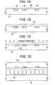
- FIGS. 1A to 1 Dare schematic diagrams showing a process for producing an SOI substrate.
- FIGS. 2A to 2 Care schematic diagrams showing a process for producing an SOI substrate.
- FIGS. 3A to 3 Dare schematic diagrams showing a process for producing a TFT.
- FIG. 4is a schematic diagram showing a structure of an electro-optical device.
- FIGS. 5A to 5 Care schematic diagrams showing a structure of a semiconductor circuit.
- FIGS. 6A to 6 Fare schematic diagrams showing various electronic apparatus.
- FIGS. 7A to 7 Dare schematic diagrams showing various electronic apparatus.
- the gist of the present inventionresides in a process for producing an SOI substrate which comprises:
- the above-mentioned processmay be modified such that the step of forming said first silicon oxide layer is followed by a step of flattening said first silicon oxide layer.
- Flatteningmay be accomplished by chemical mechanical polishing.
- Said first heat treatmentis carried out at 400-600° C. (typically 500° C.). During this heat treatment, hydrogen embrittlement takes place in the hydrogen-added layer in the direction along the hydrogen-added layer (or the direction parallel to the interface of adhering). The single-crystal semiconductor substrate is separated at this part.
- Said second heat treatmentis carried out at 900-1200° C. (typically 1050-1150° C.). At temperatures above 1100° C., the stress relaxation of Si—O—Si bonding takes place and the interface of adhering becomes stabilized.
- said second heat treatmentshould preferably be carried out in a reducing atmosphere (such as hydrogen atmosphere or hydrogen-containing atmosphere).
- a reducing atmospheresuch as hydrogen atmosphere or hydrogen-containing atmosphere.
- the hydrogen-containing atmosphereis exemplified by a hydrogen-nitrogen mixture and ammonia.
- the reducing atmosphereis not a restriction on the present invention.
- the single-crystal semiconductor substrate(from which thin film of single-crystal semiconductor is formed) undergoes stress relaxation before the adhered SOI substrate is produced.
- the vicinity of the principal surface(excluding the region which becomes an active layer afterward) is previously converted into a porous silicon layer, which relieves the stress which is generated by heat treatment when the substrate is adhered. In this way it is possible to prevent the thin film of single-crystal silicon from cracking and peeling by stress.
- the present inventionpermits the production of thin film of single-crystal silicon in good yields and hence contributes to yields of SOI substrates and TFTs with SOI substrates. This in turn leads to improved yields and reduced production costs for semiconductor devices with TFT semiconductor circuits.
- a single-crystal silicon substrate 101is made available. On its principal surface (on which elements are to be formed) is formed an insulating film, 50 nm thick, (which is a silicon oxide film in this example). The silicon oxide film is patterned to selectively form a mask 102 .
- the silicon oxide filmmay be replaced by any other insulating film, such as silicon nitride film, silicon oxynitride film, and resist mask.
- the mask 102should cover the part which becomes the active layer of TFT afterward. Also the portion covered by the mask 102 may be used for thin film of single-crystal silicon.
- the principal surface of the single-crystal silicon substrate 101undergoes anodizing treatment, so that a portion of the single-crystal silicon substrate 101 (the exposed region without the mask 102 ) is converted into a porous silicon layer 103 .
- This anodizing treatmentmay be carried out in a mixture of hydrofluoric acid and ethanol.
- the porous silicon layer 103has minute cylindrical holes in its surface in an approximate density of 10 11 /cm 2 ; however, it retains the same crystalline state (such as orientation) as that of the single-crystal silicon substrate.
- the porous silicon layer 103should preferably be formed deeper than necessary for the hydrogen-added layer to be formed later.
- the mask 102is removed, and a first silicon oxide layer 104 is formed on the single-crystal silicon substrate 101 and the porous silicon layer 103 . See FIG. 1 B.
- the forming of the first silicon oxide layer 104may be effectively preceded by heat treatment at 900-1200° C. (preferably 1000-1150° C.) in a reduction atmosphere such as a hydrogen atmosphere, an ammonia atmosphere and an inert atmosphere comprising hydrogen or ammonia (a hydrogen-nitrogen mixture, a hydrogen-argon mixture, etc.).
- a reduction atmospheresuch as a hydrogen atmosphere, an ammonia atmosphere and an inert atmosphere comprising hydrogen or ammonia (a hydrogen-nitrogen mixture, a hydrogen-argon mixture, etc.).
- This heat treatment in a reduction atmosphereblocks the surface openings of the porous silicon layer 103 by movement of silicon atoms. In other words, it provides a very flat layer resembling single-crystal silicon. This flat layer facilitates the formation of uniform silicon oxide layer in the subsequent steps.
- the first silicon oxide layer 104may be formed by any known oxidation method, such as thermal oxidation or plasma oxidation, or by any known gas phase method, such as plasma CVD, low pressure thermal CVD, and sputtering.
- the first silicon oxide layer 104 thus formedshould preferably be flattened by polishing, for example a chemical mechanical polishing or an etch-back process using a dry etching technique.
- hydrogen(to be exact, hydrogen ions) is added to the single-crystal silicon substrate 101 and the porous silicon layer 103 through the first silicon oxide layer 104 . This step forms the hydrogen-added layer 105 . See FIG. 1 C.
- hydrogen ionsmay be accomplished by means of ion implantation. Of course, it is also possible to employ other means such as plasma doping. In this example, hydrogen ions are added with a dose of 1 ⁇ 10 16 to 1 ⁇ 10 17 atoms/cm 2 .
- the depth to which the hydrogen-added layer is formedshould be accurately controlled because it determines the thickness of the single-crystal silicon thin film.
- the depth of a profile of hydrogen additionis controlled such that a single-crystal silicon layer, 50 nm thick, remains between the principal surface of the single-crystal silicon substrate 101 and the hydrogen-added layer 105 .
- the hydrogen-added layer 105traverse the porous silicon layer 103 , so that the porous silicon layer is exposed at the time of separation along the hydrogen-added layer in the subsequent step.
- Another supporting substrate 107is made available. It is a ceramic substrate having a second silicon oxide layer 106 formed thereon. This ceramic substrate may be replaced by a quartz substrate, glass ceramic substrate, semiconductor substrate (including both single-crystal and polycrystal), stainless steel substrate, or metal substrate (of Ta, W, Mo, or Ti, or an alloy thereof). The silicon oxide layer on the surface is necessary for adhering to be carried out later.
- the above-mentioned supporting substratehave an underlying layer below the second silicon oxide layer 106 .
- This underlying layermay be a metal layer or an aluminum nitride layer which has good thermal conductivity (or heat radiation). It protects the semiconductor device from thermal deterioration.
- the second silicon oxide layer 106may be formed by vapor phase deposition such as low pressure thermal CVD, sputtering, and plasma CVD. It may also be formed by thermal oxidation or plasma oxidation in the case of semiconductor substrate (e.g., single-crystal silicon substrate).
- vapor phase depositionsuch as low pressure thermal CVD, sputtering, and plasma CVD. It may also be formed by thermal oxidation or plasma oxidation in the case of semiconductor substrate (e.g., single-crystal silicon substrate).
- first substratesingle-crystal silicon substrate
- second substratesupporting substrate
- Adheringtakes place with hydrogen bonds due to moisture on the highly hydrophilic surfaces of the first and second silicon oxide layers.
- the first heat treatmentis carried out at 400-600° C. (typically 500° C.). This heat treatment causes the microvoids of the hydrogen-added layer 105 to change in volume, so that the single-crystal silicon substrate 101 is separated along the hydrogen-added layer 105 . With the single-crystal silicon substrate 101 removed, the first silicon oxide layer 104 , the single-crystal silicon layer (thin film) 109 , and the porous silicon layer 110 are left on the second silicon oxide layer 106 . See FIG. 2 A.
- the second heat treatment(or furnace annealing) is carried out at 900-1200° C. (typically 1050-1150° C.). This heat treatment relieves the stress due to Si—O—Si bond, thereby stabilizing the adhering interface. As the result, the single-crystal silicon layer 109 is completely adhered to the supporting substrate 107 . In this example, this heat treatment is carried out at 1100° C. for 2 hours in an atmosphere comprising hydrogen or an oxidizing atmosphere. See FIG. 2 B.
- the buried insulating layer 111is defined.
- the broken line in the buried insulating layer 111denotes the adhering interface where firm adhering has taken place.
- Polishingis performed to flatten the surface of the single-crystal silicon layer 109 and the porous silicon layer 110 .
- the chemical mechanical polishingis employed in this example, although any other known polishing methods may be used.
- wet etchingis performed to selectively remove the porous silicon layer 110 present near the surface of the supporting substrate 107 (or in the single-crystal silicon layer 109 ).
- a preferred etchant for this etchingis a mixed aqueous solution of hydrofluoric acid and hydrogen peroxide. It is reported that a 1:5 mixed solution of 49% HF and 30% H 2 O 2 has a selective ratio greater than 100,000 for the single-crystal silicon layer and the porous silicon layer.
- the wafer up to this stageis shown in FIG. 2 C.
- the ceramic substrate (supporting substrate) 107has the buried insulating layer 111 , on which is the single-crystal silicon layer 112 divided into a plurality of islands.
- the SOI substrateis now completed. However, it should preferably undergo heat treatment at 900-1200° C. (typically 1050-1150° C.) in a reducing atmosphere (hydrogen or hydrogen-containing atmosphere) to smooth out the surface of the single-crystal silicon layer 112 on which there still exist minute irregularities.
- This heat treatmentreduces the naturally occurred oxide film, promoting the surface diffusion of silicon atoms, thereby giving rise to a smooth surface.
- This heat treatmentalso effectively reduces the content of impurities in the single-crystal silicon layer 112 by the action of hydrogen atoms to help impurities to diffuse into the gas phase.
- the Impuritiesare phosphorus and boron which are originally contained in the single-crystal silicon substrate 101 .
- the desired SOI substrateconstructed such that a single-crystal silicon thin film divided into islands is formed on a supporting substrate having an insulating surface.
- This exampleoffers the advantage of preventing cracking and peeling due to stress because the porous silicon layer 110 functions as a stress relaxing layer in the heat treatment step (shown in FIG. 2B) for bonding. This leads to greatly improved yields in the production of SOI substrates.
- the single-crystal silicon layer(in an island shape) is formed according to the process of Example 1. It is covered with a gate insulating film 302 of silicon oxide (120 nm thick) by plasma CVD. Then, a gate electrode 303 of n-type polysilicon is formed. See FIG. 3 A.
- Dopingis performed to impart the n-type or p-type by the self-alignment process which employs the gate electrodes 303 as a mask.
- the dopantis phosphorus.
- the dopantis boron.
- This stepforms the impurity region 304 . See FIG. 3 B.
- That part of the silicon layer which is just under the gate electrodemay be doped with an impurity for reverse conductivity type (for example, boron in the case of n-type TFT) so as to control the threshold value of TFT.
- an impurity for reverse conductivity typefor example, boron in the case of n-type TFT. This doping may be accomplished through the gate electrode or previously before the gate electrode is formed.
- a side wall (side spacer) 305 of silicon oxideis formed on the gate electrode 303 by any known anisotropic etching.
- a side wall of silicon nitridemay be formed on a silicon oxide film which has previously been formed on the gate electrode 303 by plasma oxidation.
- Doping with phosphorusis performed again so as to form a region in which the concentration of impurity is higher than the above-mentioned impurity region 304 .
- the source region 306there are defined the source region 306 , the drain region 307 , the LDD (lightly doped drain) region 308 , and the channel forming region 309 . See FIG. 3 C.
- Annealingis performed to activate the impurity which has been added in the previous step and to restore the damaged silicon layer which has resulted from doping.
- This annealingmay be furnace annealing, laser annealing, or lamp annealing, or a combination thereof.
- the wafer shown in FIG. 3Cis entirely covered with a cobalt film (not shown), which subsequently undergoes thermal annealing.
- a cobalt silicide layer 310is formed.
- this cobalt filmmay be replaced by titanium film or tungsten film. This step is known and hence its detailed description is omitted.
- An interlayer insulating film 311(1 ⁇ m thick) is formed from a resin material, such as polyimide, acrylate, polyamide, polyimideamide, and benzocyclobutene (BCB).
- This insulating filmmay be silicon oxide film, silicon nitride film, or silicon oxynitride film.
- the insulating film of resin materialmay be combined with the insulating film of silicon oxide or the like.
- FIG. 3 Da TFT as shown in FIG. 3 D.
- This examplemerely illustrates one TFT structure and the application of the present invention is not limited to it. In other words, the present invention may be applied to any known structures with respect to the TFT.
- the structure shown in FIG. 3Dmay be used to form a pixel switching element for the active matrix display unit if the drain wiring 313 is electrically connected to a pixel electrode (not shown) by any known means.
- the present inventionis effective for production of electro-optical apparatus such as liquid crystal display units and electroluminescence (EL) display units.
- electro-optical apparatussuch as liquid crystal display units and electroluminescence (EL) display units.
- the present inventionmay be applied to TFTs of any structure or a variety of semiconductor circuits. That is, the present invention may be applied to any semiconductor devices with TFTs and other semiconductor circuits.
- This exampledemonstrates a liquid crystal display unit (FIG. 4) with TFT semiconductor circuits fabricated by the process in Example 2.
- the pixel TFT (or pixel switching element) and the cell assemblymay be produced by any known method; therefore, their detailed description is omitted.
- FIG. 4there are shown a supporting substrate (with an insulating surface) 11 , a pixel matrix circuit 12 , a source driver circuit 13 , a gate driver circuit 14 , a counter substrate 15 , a FPC (flexible printed circuit) 16 , and a signal processing circuit 17 .
- the signal processing circuit 17contains such processing circuits as D/A converter, gamma-correcting circuit, and signal splitting circuit, which used to be formed in an IC. Signal processing may be accomplished by means of an IC chip (with MOSFETs conventionally fabricated on a single-crystal silicon substrate) on the supporting substrate.
- the present inventionmay be applied to any electroluminescence (EL) display unit and electrochromic (EC) display unit of active matrix type.
- ELelectroluminescence
- ECelectrochromic
- the present inventioncan be applied to the entire IC technologies or to all the semiconductor circuits now on the market. For example, it can be applied to microprocessors (such as RISC processors and ASIC processors which are integrated on one chip), signal processing circuits (such as D/A converters), and high-frequency circuits for portable equipment (such as pocket telephones, PES, and mobile computers).
- microprocessorssuch as RISC processors and ASIC processors which are integrated on one chip
- signal processing circuitssuch as D/A converters
- high-frequency circuits for portable equipmentsuch as pocket telephones, PES, and mobile computers.
- FIG. 5Ashows one example of microprocessors, which is typically composed of a CPU core 21 , RAM 22 , clock controller 23 , cache memory 24 , cache controller 25 , serial interface 26 , and I/O port 27 .
- FIG. 5Ais a schematic diagram.
- the central part of any microprocessoris an IC (Integrated Circuit) 28 shown in FIG. 5 B.
- the IC 28has integrated circuits formed on a semiconductor chip 29 and protected by ceramic or the like.
- the integrated circuitsformed on a semiconductor chip 29 accord with the present invention.
- the basic unit of the semiconductor circuitsis the CMOS circuit composed of an n-channel TFT 30 and a p-channel TFT 31 as shown in FIG. 5 C. This structure saves power consumption.
- the microprocessor shown in this exampleis used as an essential part for various electronic machines and equipment, such as personal computers, portable information terminals, home appliances, and automotive and vehicular controllers.
- the present inventionmay be used to form CMOS circuits and pixel matrix circuits. These circuits may be used for various electro-optical apparatuses (such as liquid crystal display of active matrix type, EL display of active matrix type, and EC display of active matrix type). In other words, the present invention can be applied to any electronic machines and apparatus equipped with these electro-optical devices as display media.
- electro-optical apparatusessuch as liquid crystal display of active matrix type, EL display of active matrix type, and EC display of active matrix type.
- Examples of these electronic machines and apparatusinclude video cameras, digital cameras, projectors (of rear type or front type), head-mount display (goggle-type display), car navigation, personal computer, and mobile information terminals (mobile computers, pocket telephones, and electronic books). They are illustrated in FIGS. 6A to 6 F and 7 A to 7 D.
- FIG. 6Ashows a personal computer which consists of a main body 2001 , an image input 2002 , a display unit 2003 , and a keyboard 2004 .
- the present inventionmay be applied to the image input 2002 and the display unit 2003 and other signal control circuits.
- FIG. 6Bshows a video camera which consists of a main body 2101 , a display 2102 , an audio input unit 2103 , a switching unit 2104 , a battery 2105 , and an image receiver 2106 .
- the present inventionmay be applied to the display unit 2102 and the video input 2103 and other signal control circuits.
- FIG. 6Cshows a mobile computer which consists of a main body 2201 , a camera unit 2202 , an image receiver 2203 , a switching unit 2204 , and a display unit 2205 .
- the present inventionmay be applied to the display unit 2205 and other signal control circuits.
- FIG. 6Dshows a goggle type display which consists of a main body 2301 , a display unit 2302 , and arms 2303 .
- the present inventionmay be applied to the display unit 2302 and other signal control circuits.
- FIG. 6Eshows a player for a recording medium recorded programs, which consists of a main body 2401 , a display unit 2402 , a speaker 2403 , a recording medium 2404 , and a switching unit 2405 .
- this apparatusmay employ a DVD (digital versatile disc) or CD as the recording medium. It is used to enjoy music and movies and internet.
- the present inventionmay be applied to the display unit 2402 and other signal control circuits.
- FIG. 6Fshows a digital camera which consists of a main body 2501 , a display unit 2502 , an eyepiece 2503 , a switching unit 2504 , and an image receiver (not shown).
- the present inventionmay be applied to the display unit 2502 and other signal control circuits.
- FIG. 7Ashows a front-type projector which consists of a display unit 2601 and a screen 2602 .
- the present inventionmay be applied to the display unit and other signal control circuits.
- FIG. 7Bis a rear-type projector which consists of a main body 2701 , a display unit 2702 , a mirror 2703 , and a screen 2704 .
- the present inventionmay be applied to the display and other signal control circuits.
- FIG. 7Cshows an example of the structure of the display units 2601 and 2702 in FIGS. 7A and 7B, respectively.
- the display units 2601 and 2702each consist of an optical system for light source 2801 , mirrors 2802 , 2804 , 2805 and 2806 , a dichroic mirror 2803 , a prism 2807 , a liquid crystal display unit 2808 , a phase difference plate 2809 , and a projecting optical system 2810 .
- the projecting optical system 2810contains projector lenses. This example shows the one which contains three plates. The one which has a single plate may also be possible.
- the example shown in FIG. 7Cmay be modified such that the arrowed optical paths may be provided with such optical elements as lenses, polarizing film, phase difference adjusting film, and IR film.
- FIG. 7Dshows an example of the structure of the light source optical system 2801 in FIG. 7 C.
- the light source optical system 2801consists of a reflector 2811 , a light source 2812 , lens arrays 2813 and 2814 , a polarizing light converting element 2815 , and a condenser lens 2816 .
- the light source optical system shown in FIG. 7Dis illustrative only but is not limitative.
- the light source optical systemmay be provided with such optical elements as lenses, polarizing film, phase difference adjusting film, and IR film.
- the present inventionmay be applied to a broad range of fields, including almost all electronic machines and equipment.
- the electronic machines and equipment in this examplemay be realized by any combination of Examples 1 to 4.
- the present inventionit is possible to produce thin film of single-crystal silicon by Smart-Cut method without causing cracking and peeling to the thin film of single-crystal silicon during heat treatment.
- the present inventiongreatly contributes to yields and production cost of SOI substrates.
Landscapes
- Engineering & Computer Science (AREA)
- Physics & Mathematics (AREA)
- Condensed Matter Physics & Semiconductors (AREA)
- General Physics & Mathematics (AREA)
- Manufacturing & Machinery (AREA)
- Computer Hardware Design (AREA)
- Microelectronics & Electronic Packaging (AREA)
- Power Engineering (AREA)
- Thin Film Transistor (AREA)
- Element Separation (AREA)
- Liquid Crystal (AREA)
Abstract
Description
1. Field of the Invention
The present invention relates to a process for production of a thin-film transistor (TFT for short hereinafter) with single-crystal semiconductor thin film formed on a substrate having an insulating surface. The present invention relates also to a process for production of a semiconductor device containing semiconductor circuits constructed of TFTs.
The term “semiconductor device” as used in this specification embraces any device that utilizes semiconductor characteristics for its functions. To be more specific, it includes electro-optical devices typified by liquid crystal displays, semiconductor circuits formed by integration of TFTs, and electronic machines and equipment containing as parts such electro-optical devices and semiconductor circuits.
2. Description of the Relates Art
The recent rapid progress in VLSI technology has yielded SOI (silicon on insulator) which is attracting attention because of its low power consumption. This technology differs from the conventional one in that the bulk single-crystal silicon that forms the active region (or channel-forming region) of FET is replaced by thin-film single-crystal silicon.
An SOI substrate consists of single-crystal silicon and thin film of single-crystal silicon formed thereon, with a buried silicon oxide film interposed between them. There are several known methods for its production. A new technology that is attracting attention is a bonded SOI substrate which is produced by bonding together two silicon substrates. This technology is expected to form thin film of single-crystal silicon on a glass substrate or the like.
The most noticeable among the technologies of bonded SOI substrate is “Smart-Cut” (a registered trademark of SOITEC Co., Ltd.). It utilizes the hydrogen brittleness. For more detail, refer to “Electronic material”, pp. 83-87, August, 1997, issued by Kogyo Chosa kai.
The “Smart-Cut” process consists of forming thin film of single-crystal silicon on a silicon substrate as a support by heat treatment in two steps. The first heat treatment is performed at 400-600° C. so as to bring about hydrogen embrittlement and separate thin film of single-crystal silicon, and the second heat treatment is performed at about 1100° C. so as to stabilize the bonding interface.
The disadvantage of this process is that the second heat treatment causes a strong stress to occur in the thin film of single-crystal silicon and this stress causes the thin film of single-crystal silicon to crack and peel at the edges of the silicon substrate. This is a serious problem with “Smart-Cut” process, and an effective solution to it is required.
The present invention was completed to address the above-mentioned problem. Thus, it is an object of the present invention to provide a process for producing a bonded SOI substrate without causing cracking and peeling to the thin film of single-crystal semiconductor.
The present invention will contribute to the yield and production cost of TFTs formed on an SOI substrate and in turn contribute to the yield and production cost of semiconductor circuits and electro-optical devices with TFTs. Moreover, the present invention will contribute to the yield and production cost of electronic machines equipped with said semiconductor circuits and electro-optical devices.
FIGS. 1A to1D are schematic diagrams showing a process for producing an SOI substrate.
FIGS. 2A to2C are schematic diagrams showing a process for producing an SOI substrate.
FIGS. 3A to3D are schematic diagrams showing a process for producing a TFT.
FIG. 4 is a schematic diagram showing a structure of an electro-optical device.
FIGS. 5A to5C are schematic diagrams showing a structure of a semiconductor circuit.
FIGS. 6A to6F are schematic diagrams showing various electronic apparatus.
FIGS. 7A to7D are schematic diagrams showing various electronic apparatus.
The gist of the present invention resides in a process for producing an SOI substrate which comprises:
a step of forming on the principal surface of a single-crystal semiconductor substrate an insulating film and performing patterning on said insulating film, thereby selectively forming a mask;
a step of converting by anodizing treatment a portion of said single-crystal semiconductor substrate into a porous silicon layer;
a step of removing said mask;
a step of forming on the principal surface of said single-crystal semiconductor substrate and said porous silicon layer a first silicon oxide layer;
a step of adding hydrogen into said single-crystal semiconductor substrate and said porous silicon layer through said first silicon oxide layer, thereby forming a hydrogen-added layer;
a step of adhering together said single-crystal semiconductor substrate and a supporting substrate provided with a second silicon oxide layer thereon;
a step of performing a first heat treatment, thereby separating said single-crystal semiconductor substrate along said hydrogen-added layer;
a step of performing a second heat treatment at 900-1200° C.; and
a step of removing the porous silicon layer present near the surface of said supporting substrate.
The above-mentioned process may be modified such that the step of forming said first silicon oxide layer is followed by a step of flattening said first silicon oxide layer. Flattening may be accomplished by chemical mechanical polishing.
Said first heat treatment is carried out at 400-600° C. (typically 500° C.). During this heat treatment, hydrogen embrittlement takes place in the hydrogen-added layer in the direction along the hydrogen-added layer (or the direction parallel to the interface of adhering). The single-crystal semiconductor substrate is separated at this part.
Said second heat treatment is carried out at 900-1200° C. (typically 1050-1150° C.). At temperatures above 1100° C., the stress relaxation of Si—O—Si bonding takes place and the interface of adhering becomes stabilized.
In the above-mentioned process, said second heat treatment should preferably be carried out in a reducing atmosphere (such as hydrogen atmosphere or hydrogen-containing atmosphere). The hydrogen-containing atmosphere is exemplified by a hydrogen-nitrogen mixture and ammonia. The reducing atmosphere is not a restriction on the present invention.
What is most important in the process of the present invention is that the single-crystal semiconductor substrate (from which thin film of single-crystal semiconductor is formed) undergoes stress relaxation before the adhered SOI substrate is produced.
In other words, the vicinity of the principal surface (excluding the region which becomes an active layer afterward) is previously converted into a porous silicon layer, which relieves the stress which is generated by heat treatment when the substrate is adhered. In this way it is possible to prevent the thin film of single-crystal silicon from cracking and peeling by stress.
Therefore, the present invention permits the production of thin film of single-crystal silicon in good yields and hence contributes to yields of SOI substrates and TFTs with SOI substrates. This in turn leads to improved yields and reduced production costs for semiconductor devices with TFT semiconductor circuits.
The invention will be described in more detail with reference to the following examples.
The process of the invention is explained with reference to FIGS. 1A to1D and FIGS. 2A to2C. First, a single-crystal silicon substrate 101 is made available. On its principal surface (on which elements are to be formed) is formed an insulating film, 50 nm thick, (which is a silicon oxide film in this example). The silicon oxide film is patterned to selectively form amask 102. The silicon oxide film may be replaced by any other insulating film, such as silicon nitride film, silicon oxynitride film, and resist mask.
Themask 102 should cover the part which becomes the active layer of TFT afterward. Also the portion covered by themask 102 may be used for thin film of single-crystal silicon.
The principal surface of the single-crystal silicon substrate 101 undergoes anodizing treatment, so that a portion of the single-crystal silicon substrate101 (the exposed region without the mask102) is converted into aporous silicon layer 103. This anodizing treatment may be carried out in a mixture of hydrofluoric acid and ethanol. Theporous silicon layer 103 has minute cylindrical holes in its surface in an approximate density of 1011/cm2; however, it retains the same crystalline state (such as orientation) as that of the single-crystal silicon substrate. Theporous silicon layer 103 should preferably be formed deeper than necessary for the hydrogen-added layer to be formed later.
Themask 102 is removed, and a firstsilicon oxide layer 104 is formed on the single-crystal silicon substrate 101 and theporous silicon layer 103. See FIG.1B.
The forming of the first silicon oxide layer104 (that follows the removal of the mask102) may be effectively preceded by heat treatment at 900-1200° C. (preferably 1000-1150° C.) in a reduction atmosphere such as a hydrogen atmosphere, an ammonia atmosphere and an inert atmosphere comprising hydrogen or ammonia (a hydrogen-nitrogen mixture, a hydrogen-argon mixture, etc.).
This heat treatment in a reduction atmosphere blocks the surface openings of theporous silicon layer 103 by movement of silicon atoms. In other words, it provides a very flat layer resembling single-crystal silicon. This flat layer facilitates the formation of uniform silicon oxide layer in the subsequent steps.
The firstsilicon oxide layer 104 may be formed by any known oxidation method, such as thermal oxidation or plasma oxidation, or by any known gas phase method, such as plasma CVD, low pressure thermal CVD, and sputtering. The firstsilicon oxide layer 104 thus formed should preferably be flattened by polishing, for example a chemical mechanical polishing or an etch-back process using a dry etching technique.
In the state shown in FIG. 1B, hydrogen (to be exact, hydrogen ions) is added to the single-crystal silicon substrate 101 and theporous silicon layer 103 through the firstsilicon oxide layer 104. This step forms the hydrogen-addedlayer 105. See FIG.1C.
The addition of hydrogen ions may be accomplished by means of ion implantation. Of course, it is also possible to employ other means such as plasma doping. In this example, hydrogen ions are added with a dose of 1×10¹⁶to 1×10¹⁷atoms/cm2.
The depth to which the hydrogen-added layer is formed should be accurately controlled because it determines the thickness of the single-crystal silicon thin film. In this example, the depth of a profile of hydrogen addition is controlled such that a single-crystal silicon layer, 50 nm thick, remains between the principal surface of the single-crystal silicon substrate 101 and the hydrogen-addedlayer 105.
It is desirable that the hydrogen-addedlayer 105 traverse theporous silicon layer 103, so that the porous silicon layer is exposed at the time of separation along the hydrogen-added layer in the subsequent step.
Another supportingsubstrate 107 is made available. It is a ceramic substrate having a secondsilicon oxide layer 106 formed thereon. This ceramic substrate may be replaced by a quartz substrate, glass ceramic substrate, semiconductor substrate (including both single-crystal and polycrystal), stainless steel substrate, or metal substrate (of Ta, W, Mo, or Ti, or an alloy thereof). The silicon oxide layer on the surface is necessary for adhering to be carried out later.
It is desirable that the above-mentioned supporting substrate have an underlying layer below the secondsilicon oxide layer 106. This underlying layer may be a metal layer or an aluminum nitride layer which has good thermal conductivity (or heat radiation). It protects the semiconductor device from thermal deterioration.
The secondsilicon oxide layer 106 may be formed by vapor phase deposition such as low pressure thermal CVD, sputtering, and plasma CVD. It may also be formed by thermal oxidation or plasma oxidation in the case of semiconductor substrate (e.g., single-crystal silicon substrate).
Now, the first substrate (single-crystal silicon substrate) and the second substrate (supporting substrate) are ready. They are bonded together, with their principal surfaces facing each other. In other words, the firstsilicon oxide layer 104 and the secondsilicon oxide layer 106 are adhered together. See FIG.1D.
Adhering takes place with hydrogen bonds due to moisture on the highly hydrophilic surfaces of the first and second silicon oxide layers.
The first heat treatment is carried out at 400-600° C. (typically 500° C.). This heat treatment causes the microvoids of the hydrogen-addedlayer 105 to change in volume, so that the single-crystal silicon substrate 101 is separated along the hydrogen-addedlayer 105. With the single-crystal silicon substrate 101 removed, the firstsilicon oxide layer 104, the single-crystal silicon layer (thin film)109, and theporous silicon layer 110 are left on the secondsilicon oxide layer 106. See FIG.2A.
The second heat treatment (or furnace annealing) is carried out at 900-1200° C. (typically 1050-1150° C.). This heat treatment relieves the stress due to Si—O—Si bond, thereby stabilizing the adhering interface. As the result, the single-crystal silicon layer 109 is completely adhered to the supportingsubstrate 107. In this example, this heat treatment is carried out at 1100° C. for 2 hours in an atmosphere comprising hydrogen or an oxidizing atmosphere. See FIG.2B.
As the bonding interface becomes stabilized, the buried insulatinglayer 111 is defined. In FIG. 2B, the broken line in the buried insulatinglayer 111 denotes the adhering interface where firm adhering has taken place.
Polishing is performed to flatten the surface of the single-crystal silicon layer 109 and theporous silicon layer 110. The chemical mechanical polishing is employed in this example, although any other known polishing methods may be used.
Wet etching is performed to selectively remove theporous silicon layer 110 present near the surface of the supporting substrate107 (or in the single-crystal silicon layer109). A preferred etchant for this etching is a mixed aqueous solution of hydrofluoric acid and hydrogen peroxide. It is reported that a 1:5 mixed solution of 49% HF and 30% H2O2has a selective ratio greater than 100,000 for the single-crystal silicon layer and the porous silicon layer.
The wafer up to this stage is shown in FIG.2C. The ceramic substrate (supporting substrate)107 has the buried insulatinglayer 111, on which is the single-crystal silicon layer 112 divided into a plurality of islands.
The SOI substrate is now completed. However, it should preferably undergo heat treatment at 900-1200° C. (typically 1050-1150° C.) in a reducing atmosphere (hydrogen or hydrogen-containing atmosphere) to smooth out the surface of the single-crystal silicon layer 112 on which there still exist minute irregularities. This heat treatment reduces the naturally occurred oxide film, promoting the surface diffusion of silicon atoms, thereby giving rise to a smooth surface.
This heat treatment also effectively reduces the content of impurities in the single-crystal silicon layer 112 by the action of hydrogen atoms to help impurities to diffuse into the gas phase. The Impurities are phosphorus and boron which are originally contained in the single-crystal silicon substrate 101.
Thus there is obtained the desired SOI substrate constructed such that a single-crystal silicon thin film divided into islands is formed on a supporting substrate having an insulating surface. This example offers the advantage of preventing cracking and peeling due to stress because theporous silicon layer 110 functions as a stress relaxing layer in the heat treatment step (shown in FIG. 2B) for bonding. This leads to greatly improved yields in the production of SOI substrates.
This example demonstrates, with reference to FIG. 3, the fabrication of TFT on the single-crystal silicon layer (in an island shape) which was formed by the process in Example 1.
First, the single-crystal silicon layer (in an island shape) is formed according to the process of Example 1. It is covered with agate insulating film 302 of silicon oxide (120 nm thick) by plasma CVD. Then, agate electrode 303 of n-type polysilicon is formed. See FIG.3A.
Doping is performed to impart the n-type or p-type by the self-alignment process which employs thegate electrodes 303 as a mask. (In this example to fabricate n-type TFTs, the dopant is phosphorus. For p-type TFTs, the dopant is boron.) This step forms theimpurity region 304. See FIG.3B.
That part of the silicon layer which is just under the gate electrode may be doped with an impurity for reverse conductivity type (for example, boron in the case of n-type TFT) so as to control the threshold value of TFT. This doping may be accomplished through the gate electrode or previously before the gate electrode is formed.
On thegate electrode 303 is formed a side wall (side spacer)305 of silicon oxide by any known anisotropic etching. Alternatively, a side wall of silicon nitride may be formed on a silicon oxide film which has previously been formed on thegate electrode 303 by plasma oxidation.
Doping with phosphorus is performed again so as to form a region in which the concentration of impurity is higher than the above-mentionedimpurity region 304. As the result of these two doping steps, there are defined thesource region 306, thedrain region 307, the LDD (lightly doped drain)region 308, and thechannel forming region 309. See FIG.3C.
Annealing is performed to activate the impurity which has been added in the previous step and to restore the damaged silicon layer which has resulted from doping. This annealing may be furnace annealing, laser annealing, or lamp annealing, or a combination thereof.
The wafer shown in FIG. 3C is entirely covered with a cobalt film (not shown), which subsequently undergoes thermal annealing. Thus, acobalt silicide layer 310 is formed. Incidentally, this cobalt film may be replaced by titanium film or tungsten film. This step is known and hence its detailed description is omitted.
An interlayer insulating film311 (1 μm thick) is formed from a resin material, such as polyimide, acrylate, polyamide, polyimideamide, and benzocyclobutene (BCB). This insulating film may be silicon oxide film, silicon nitride film, or silicon oxynitride film. The insulating film of resin material may be combined with the insulating film of silicon oxide or the like.
Contact holes are made in theinterlayer insulating film 311, and thesource wiring 312 and thedrain wiring 313 are formed from aluminum. Finally, furnace annealing is performed (for hydrogenation) on the entire element in a hydrogen atmosphere at 350° C. for 2 hours.
Thus there is obtained a TFT as shown in FIG.3D. This example merely illustrates one TFT structure and the application of the present invention is not limited to it. In other words, the present invention may be applied to any known structures with respect to the TFT.
The structure shown in FIG. 3D may be used to form a pixel switching element for the active matrix display unit if thedrain wiring 313 is electrically connected to a pixel electrode (not shown) by any known means.
In other words, the present invention is effective for production of electro-optical apparatus such as liquid crystal display units and electroluminescence (EL) display units.
As mentioned above, the present invention may be applied to TFTs of any structure or a variety of semiconductor circuits. That is, the present invention may be applied to any semiconductor devices with TFTs and other semiconductor circuits.
This example demonstrates a liquid crystal display unit (FIG. 4) with TFT semiconductor circuits fabricated by the process in Example 2. The pixel TFT (or pixel switching element) and the cell assembly may be produced by any known method; therefore, their detailed description is omitted.
In FIG. 4, there are shown a supporting substrate (with an insulating surface)11, apixel matrix circuit 12, asource driver circuit 13, agate driver circuit 14, acounter substrate 15, a FPC (flexible printed circuit)16, and asignal processing circuit 17.
Thesignal processing circuit 17 contains such processing circuits as D/A converter, gamma-correcting circuit, and signal splitting circuit, which used to be formed in an IC. Signal processing may be accomplished by means of an IC chip (with MOSFETs conventionally fabricated on a single-crystal silicon substrate) on the supporting substrate.
Although this example demonstrates a liquid crystal display unit, the present invention may be applied to any electroluminescence (EL) display unit and electrochromic (EC) display unit of active matrix type.
This example demonstrates merely a liquid crystal display unit; the application of the present invention is not limited to it.
The present invention can be applied to the entire IC technologies or to all the semiconductor circuits now on the market. For example, it can be applied to microprocessors (such as RISC processors and ASIC processors which are integrated on one chip), signal processing circuits (such as D/A converters), and high-frequency circuits for portable equipment (such as pocket telephones, PES, and mobile computers).
FIG. 5A shows one example of microprocessors, which is typically composed of aCPU core 21,RAM 22,clock controller 23,cache memory 24,cache controller 25,serial interface 26, and I/O port 27.
Actual microprocessors greatly vary in circuit design depending on their use. (FIG. 5A is a schematic diagram.) The central part of any microprocessor is an IC (Integrated Circuit)28 shown in FIG.5B. TheIC 28 has integrated circuits formed on asemiconductor chip 29 and protected by ceramic or the like.
The integrated circuits (or semiconductor circuits) formed on asemiconductor chip 29 accord with the present invention. In this example, the basic unit of the semiconductor circuits is the CMOS circuit composed of an n-channel TFT 30 and a p-channel TFT 31 as shown in FIG.5C. This structure saves power consumption.
The microprocessor shown in this example is used as an essential part for various electronic machines and equipment, such as personal computers, portable information terminals, home appliances, and automotive and vehicular controllers.
The present invention may be used to form CMOS circuits and pixel matrix circuits. These circuits may be used for various electro-optical apparatuses (such as liquid crystal display of active matrix type, EL display of active matrix type, and EC display of active matrix type). In other words, the present invention can be applied to any electronic machines and apparatus equipped with these electro-optical devices as display media.
Examples of these electronic machines and apparatus include video cameras, digital cameras, projectors (of rear type or front type), head-mount display (goggle-type display), car navigation, personal computer, and mobile information terminals (mobile computers, pocket telephones, and electronic books). They are illustrated in FIGS. 6A to6F and7A to7D.
FIG. 6A shows a personal computer which consists of amain body 2001, animage input 2002, adisplay unit 2003, and akeyboard 2004. The present invention may be applied to theimage input 2002 and thedisplay unit 2003 and other signal control circuits.
FIG. 6B shows a video camera which consists of amain body 2101, adisplay 2102, anaudio input unit 2103, aswitching unit 2104, abattery 2105, and animage receiver 2106. The present invention may be applied to thedisplay unit 2102 and thevideo input 2103 and other signal control circuits.
FIG. 6C shows a mobile computer which consists of amain body 2201, acamera unit 2202, animage receiver 2203, aswitching unit 2204, and adisplay unit 2205. The present invention may be applied to thedisplay unit 2205 and other signal control circuits.
FIG. 6D shows a goggle type display which consists of amain body 2301, adisplay unit 2302, andarms 2303. The present invention may be applied to thedisplay unit 2302 and other signal control circuits.
FIG. 6E shows a player for a recording medium recorded programs, which consists of amain body 2401, adisplay unit 2402, aspeaker 2403, arecording medium 2404, and aswitching unit 2405. Incidentally, this apparatus may employ a DVD (digital versatile disc) or CD as the recording medium. It is used to enjoy music and movies and internet. The present invention may be applied to thedisplay unit 2402 and other signal control circuits.
FIG. 6F shows a digital camera which consists of amain body 2501, adisplay unit 2502, an eyepiece2503, a switching unit2504, and an image receiver (not shown). The present invention may be applied to thedisplay unit 2502 and other signal control circuits.
FIG. 7A shows a front-type projector which consists of adisplay unit 2601 and ascreen 2602. The present invention may be applied to the display unit and other signal control circuits.
FIG. 7B is a rear-type projector which consists of amain body 2701, adisplay unit 2702, amirror 2703, and ascreen 2704. The present invention may be applied to the display and other signal control circuits.
FIG. 7C shows an example of the structure of thedisplay units display units light source 2801, mirrors2802,2804,2805 and2806, adichroic mirror 2803, aprism 2807, a liquidcrystal display unit 2808, aphase difference plate 2809, and a projectingoptical system 2810. The projectingoptical system 2810 contains projector lenses. This example shows the one which contains three plates. The one which has a single plate may also be possible. Incidentally, the example shown in FIG. 7C may be modified such that the arrowed optical paths may be provided with such optical elements as lenses, polarizing film, phase difference adjusting film, and IR film.
FIG. 7D shows an example of the structure of the light sourceoptical system 2801 in FIG.7C. The light sourceoptical system 2801 consists of areflector 2811, alight source 2812,lens arrays light converting element 2815, and acondenser lens 2816. The light source optical system shown in FIG. 7D is illustrative only but is not limitative. For example, the light source optical system may be provided with such optical elements as lenses, polarizing film, phase difference adjusting film, and IR film.
As mentioned above, the present invention may be applied to a broad range of fields, including almost all electronic machines and equipment. And, the electronic machines and equipment in this example may be realized by any combination of Examples 1 to 4.
According to the present invention, it is possible to produce thin film of single-crystal silicon by Smart-Cut method without causing cracking and peeling to the thin film of single-crystal silicon during heat treatment. In other words, the present invention greatly contributes to yields and production cost of SOI substrates.
This in turn leads to improved yields and reduced production costs of semiconductor devices with TFT semiconductor circuits.
Claims (60)
1. A method for manufacturing a semiconductor device comprising the steps of:
forming an insulating film on one surface of a single-crystal semiconductor substrate;
patterning said insulating film, thereby selectively forming a mask;
converting a portion of said single-crystal semiconductor substrate into at least one porous layer by using an anodizing treatment;
removing said mask;
forming a first silicon oxide layer on said one surface;
polishing a surface of said first silicon oxide layer;
adding hydrogen into said single-crystal semiconductor substrate and said porous layer through said first silicon oxide layer, thereby forming a hydrogen-added layer;
adhering together said single-crystal semiconductor substrate and a supporting substrate provided with a second silicon oxide layer thereon;
performing a first heat treatment, thereby separating said single-crystal semiconductor substrate and said porous layer along said hydrogen-added layer;
performing a second heat treatment of said supporting substrate at 900-1200° C.; and
removing said porous layer present over said supporting substrate.
2. A method for manufacturing a semiconductor device according toclaim 1 , wherein said surface is polished by chemical mechanical polishing.
3. A method for manufacturing a semiconductor device according toclaim 1 , wherein the step of forming said mask is designed to form in a region which becomes afterward an active region of a thin film transistor.
4. A method for manufacturing a semiconductor device according toclaim 1 , wherein said supporting substrate is selected from the group consisting of a semiconductor substrate, a quartz substrate, a ceramic substrate, a metal substrate, and a stainless steel substrate.
5. A method for manufacturing a semiconductor device according toclaim 1 , wherein said semiconductor device is an electroluminenscence display unit.
6. A method for manufacturing a semiconductor device according toclaim 1 , wherein said semiconductor device is an integrated circuit.
7. A method for manufacturing a semiconductor device according toclaim 1 , wherein said semiconductor device is a liquid crystal display unit.
8. A method for manufacturing a semiconductor device according toclaim 1 , wherein said semiconductor device is a display unit incorporated in one selected from a personal computer, a video camera, a mobile computer, a digital camera, a player for a recording medium, a goggle type display, a front type projector and a rear type projector.
9. A method for manufacturing a semiconductor device comprising the steps of:
forming an insulating film on one surface of a single-crystal semiconductor substrate;
patterning said insulating film, thereby selectively forming a mask;
converting a portion of said single-crystal semiconductor substrate into at least one porous layer by using an anodizing treatment;
removing said mask;
forming a first silicon oxide layer on said one surface;
polishing a surface of said first silicon oxide layer;
adding hydrogen into said single-crystal semiconductor substrate and said porous layer through said first silicon oxide layer, thereby forming a hydrogen-added layer;
adhering together said single-crystal semiconductor substrate and a supporting substrate provided with a second silicon oxide layer thereon;
performing a first heat treatment, thereby separating said single-crystal semiconductor substrate and said porous layer along said hydrogen-added layer;
performing a second heat treatment of said supporting substrate at 900-1200° C.;
removing said porous layer present over said supporting substrate, thereby forming at least one island-like semiconductor layer over said supporting substrate;
forming a gate electrode over said island-like semiconductor layer; and
introducing a p-type or an n-type impurity into said island-like semiconductor layer to form at least a source region, a drain region and a channel region.
10. A method for manufacturing a semiconductor device according toclaim 9 , wherein said surface is polished by chemical mechanical polishing.
11. A method for manufacturing a semiconductor device according toclaim 9 , wherein the step of forming said mask is designed to form in a region which becomes afterward said island-like semiconductor layer constituting a thin film transistor.
12. A method for manufacturing a semiconductor device according toclaim 9 , wherein said supporting substrate is selected from the group consisting of a semiconductor substrate, a quartz substrate, a ceramic substrate, a metal substrate, and a stainless steel substrate.
13. A method for manufacturing a semiconductor device according toclaim 9 , wherein said semiconductor device is an electroluminescence display unit.
14. A method for manufacturing a semiconductor device according toclaim 9 , wherein said semiconductor device is an integrated circuit.
15. A method for manufacturing a semiconductor device according toclaim 9 , wherein said semiconductor device is a liquid crystal display unit.
16. A method for manufacturing a semiconductor device according toclaim 9 , wherein said semiconductor device is a display unit incorporated in one selected from a personal computer, a video camera, a mobile computer, a digital camera, a player for a recording medium, a goggle type display, a front type projector and a rear type projector.
17. A method for manufacturing a semiconductor device comprising the steps of:
forming an insulating film on one surface of a single-crystal semiconductor substrate;
patterning said insulating film, thereby selectively forming a mask;
converting a portion of said single-crystal semiconductor substrate into at least one porous layer by using an anodizing treatment;
removing said mask;
forming a first silicon oxide layer on said one surface;
polishing a surface of said first silicon oxide layer;
adding hydrogen into said single-crystal semiconductor substrate and said porous layer through said first silicon oxide layer, thereby forming a hydrogen-added layer;
adhering together said single-crystal semiconductor substrate and a supporting substrate provided with a second silicon oxide layer thereon;
performing a first heat treatment, thereby separating said single-crystal semiconductor substrate and said porous layer along said hydrogen-added layer;
performing a second heat treatment of said supporting substrate at 900-1200° C.;
removing said porous present over said supporting substrate, thereby forming at least one island-like semiconductor layer over said supporting substrate;
forming a gate electrode over said island-like semiconductor layer;
introducing a p-type or an n-type impurity into said island-like semiconductor layer to form at least a source region, a drain region, a lightly doped drain region and a channel region;
forming an interlayer insulating film to cover said gate electrode and said island-like semiconductor layer;
forming a source wiring and a drain wiring in contact with said source region and said drain region, respectively.
18. A method for manufacturing a semiconductor device according toclaim 17 , wherein said surface is polished by chemical mechanical polishing.
19. A method for manufacturing a semiconductor device according toclaim 17 , wherein the step of forming said mask is designed to form in a region which becomes afterward said island-like semiconductor layer constituting a thin film transistor.
20. A method for manufacturing a semiconductor device according toclaim 17 , wherein said supporting substrate is selected from the group consisting of a semiconductor substrate, a quartz substrate, a ceramic substrate, a metal substrate, and a stainless steel substrate.
21. A method for manufacturing a semiconductor device according toclaim 17 , wherein said semiconductor device is an electroluminescence display unit.
22. A method for manufacturing a semiconductor device according toclaim 17 , wherein said semiconductor device is an integrated circuit.
23. A method for manufacturing a semiconductor device according toclaim 17 , wherein said semiconductor device is a liquid crystal display unit.
24. A method for manufacturing a semiconductor device according toclaim 17 , wherein said semiconductor device is a display unit incorporated in one selected from a personal computer, a video camera, a mobile computer, a digital camera, a player for a recording medium, a goggle type display, a front type projector and a rear type projector.
25. A method for manufacturing a semiconductor device comprising the steps of:
forming a mask on one surface of a single-crystal semiconductor substrate;
converting a portion of said one surface into at least one porous layer by using an anodizing treatment, wherein said mask is not formed on said portion;
removing said mask;
forming a first silicon oxide layer on said one surface; polishing a surface of said first silicon oxide layer;
adding hydrogen into said single-crystal semiconductor substrate through said first silicon oxide layer, thereby forming a hydrogen-added layer;
adhering together said single-crystal semiconductor substrate and a supporting substrate provided with a second silicon oxide layer thereon;
performing a first heat treatment, thereby separating said single-crystal semiconductor substrate along said hydrogen-added layer;
performing a second heat treatment of said supporting substrate at 900-1200° C.; and
removing said porous layer present over said supporting substrate.
26. A method for manufacturing a semiconductor device according toclaim 25 , wherein the step of forming said first silicon oxide layer is followed by a step of flattening said first silicon oxide layer.
27. A method for manufacturing a semiconductor device according toclaim 25 , wherein the step of forming said mask is designed to form in a region which becomes afterward an active region of a thin film transistor.
28. A method for manufacturing a semiconductor device according toclaim 25 , wherein said supporting substrate is selected from the group consisting of a semiconductor substrate, a quartz substrate, a ceramic substrate, a metal substrate, and a stainless steel substrate.
29. A method for manufacturing a semiconductor device according toclaim 25 , wherein said semiconductor device is an electroluminescence display unit.
30. A method for manufacturing a semiconductor device according toclaim 25 , wherein said semiconductor device is an integrated circuit.
31. A method for manufacturing a semiconductor device according toclaim 25 , wherein said semiconductor device is a liquid crystal display unit.
32. A method for manufacturing a semiconductor device according toclaim 25 , wherein said semiconductor device is a display unit incorporated in one selected from a personal computer, a video camera, a mobile computer, a digital camera, a player for a recording medium, a goggle type display, a front type projector and a rear type projector.
33. A method for manufacturing a display device comprising the steps of:
forming an insulating film on one surface of a single-crystal semiconductor substrate;
patterning said insulating film, thereby selectively forming a mask;
converting a portion of said single-crystal semiconductor substrate into at least one porous layer by using an anodizing treatment;
removing said mask;
forming a first silicon oxide layer on said one surface;
adding hydrogen into said single-crystal semiconductor substrate and said porous layer through said first silicon oxide layer, thereby forming a hydrogen-added layer;
adhering together said single-crystal semiconductor substrate and a supporting substrate provided with a second silicon oxide layer thereon;
performing a first heat treatment, thereby separating said single-crystal semiconductor substrate and said porous layer along said hydrogen-added layer;
performing a second heat treatment of said supporting substrate at 900-1200° C.; and
removing said porous layer present over said supporting substrate.
34. A method for manufacturing a display device according toclaim 33 , wherein said surface is polished by chemical mechanical polishing.
35. A method for manufacturing a display device according toclaim 33 , wherein the step of forming said mask is designed to form in a region which becomes afterward an active region of a thin film transistor.
36. A method for manufacturing a semiconductor device according toclaim 33 , wherein said supporting substrate is selected from the group consisting of a semiconductor substrate, a quartz substrate, a ceramic substrate, a metal substrate, and a stainless steel substrate.
37. A method for manufacturing a display device according toclaim 33 , wherein said semiconductor device is an electroluminescence display unit.
38. A method for manufacturing a semiconductor device according toclaim 33 , wherein said semiconductor device is a liquid crystal display unit.
39. A method for manufacturing a personal computer comprising the steps of:
forming an insulating film on one surface of a single-crystal semiconductor substrate;
patterning said insulating film, thereby selectively forming a mask;
converting a portion of said single-crystal semiconductor substrate into at least one porous layer by using an anodizing treatment;
removing said mask;
forming a first silicon oxide layer on said one surface;
adding hydrogen into said single-crystal semiconductor substrate and said porous layer through said first silicon oxide layer, thereby forming a hydrogen-added layer;
adhering together said single-crystal semiconductor substrate and a supporting substrate provided with a second silicon oxide layer thereon;
performing a first heat treatment, thereby separating said single-crystal semiconductor substrate and said porous layer along said hydrogen-added layer;
performing a second heat treatment of said supporting substrate at 900-1200° C.; and
removing said porous layer present over said supporting substrate.
40. A method for manufacturing a display device according toclaim 39 , wherein said surface is polished by chemical mechanical polishing.
41. A method for manufacturing a personal computer according toclaim 39 , wherein the step of forming said mask is designed to form in a region which becomes afterward an active region of a thin film transistor.
42. A method for manufacturing a semiconductor device according toclaim 39 , wherein said supporting substrate is selected from the group consisting of a semiconductor substrate, a quartz substrate, a ceramic substrate, a metal substrate, and a stainless steel substrate.
43. A method for manufacturing a personal computer according toclaim 39 , wherein said semiconductor device is an electroluminescence display unit.
44. A method for manufacturing a personal computer according toclaim 39 , wherein said semiconductor device is a liquid crystal display unit.
45. A method for manufacturing a semiconductor device comprising the steps of:
forming an insulating film on one surface of a single-crystal semiconductor substrate;
patterning said insulating film, thereby selectively forming a mask;
converting a portion of said single-crystal semiconductor substrate into at least one porous layer by using an anodizing treatment;
removing said mask;
forming a first silicon oxide layer on said one surface;
polishing a surface of said first silicon oxide layer;
adding hydrogen into said single-crystal semiconductor substrate and said porous layer through said first silicon oxide layer, thereby forming a hydrogen-added layer;
adhering together said single-crystal semiconductor substrate and a supporting substrate provided with a second silicon oxide layer thereon;
performing a first heat treatment, thereby separating said single-crystal semiconductor substrate and said porous layer along said hydrogen-added layer; and
removing said porous layer present over said supporting substrate.
46. A method for manufacturing a semiconductor device comprising the steps of:
forming an insulating film on one surface of a single-crystal semiconductor substrate;
patterning said insulating film, thereby selectively forming a mask;
converting a portion of said single-crystal semiconductor substrate into at least one porous layer by using an anodizing treatment;
removing said mask;
forming a first silicon oxide layer on said one surface;
polishing a surface of said first silicon oxide layer;
adding hydrogen into said single-crystal semiconductor substrate and said porous layer through said first silicon oxide layer, thereby forming a hydrogen-added layer;
adhering together said single-crystal semiconductor substrate and a supporting substrate provided with a second silicon oxide layer thereon;
performing a first heat treatment, thereby separating said single-crystal semiconductor substrate and said porous layer along said hydrogen-added layer;
removing said porous layer present over said supporting substrate, thereby forming at least one island-like semiconductor layer over said supporting substrate;
forming a gate electrode over said island-like semiconductor layer; and
introducing a p-type or an n-type impurity into said island-like semiconductor layer to form at least a source region, a drain region and a channel region.
47. A method for manufacturing a semiconductor device according to claim45, wherein said surface is polished by chemical mechanical polishing.
48. A method for manufacturing a semiconductor device according toclaim 46 , wherein said surface is polished by chemical mechanical polishing.
49. A method for manufacturing a semiconductor device according toclaim 45 , wherein the step of forming said mask is designed to form in a region which becomes afterward an active region of a thin film transistor.
50. A method for manufacturing a semiconductor device according toclaim 46 , wherein the step of forming said mask is designed to form in a region which becomes afterward said island-like semiconductor layer constituting a thin film transistor.
51. A method for manufacturing a semiconductor device according toclaim 45 , wherein said supporting substrate is selected from the group consisting of a semiconductor substrate, a quartz substrate, a ceramic substrate, a metal substrate, and a stainless steel substrate.
52. A method for manufacturing a semiconductor device according toclaim 46 , wherein said supporting substrate is selected from the group consisting of a semiconductor substrate, a quartz substrate, a ceramic substrate, a metal substrate, and a stainless steel substrate.
53. A method for manufacturing a semiconductor device according toclaim 45 , wherein said semiconductor device is an electroluminenscence display unit.
54. A method for manufacturing a semiconductor device according toclaim 46 , wherein said semiconductor device is an electroluminenscence display unit.
55. A method for manufacturing a semiconductor device according toclaim 45 , wherein said semiconductor device is an integrated circuit.
56. A method for manufacturing a semiconductor device according toclaim 46 , wherein said semiconductor device is an integrated circuit.
57. A method for manufacturing a semiconductor device according toclaim 45 , wherein said semiconductor device is a liquid crystal display unit.
58. A method for manufacturing a semiconductor device according toclaim 46 , wherein said semiconductor device is a liquid crystal display unit.
59. A method for manufacturing a semiconductor device according toclaim 45 , wherein said semiconductor device is a display unit incorporated in one selected from a personal computer, a video camera, a mobile computer, a digital camera, a player for a recording medium, a goggle type display, a front type projector and a rear type projector.
60. A method for manufacturing a semiconductor device according toclaim 46 , wherein said semiconductor device is a display unit incorporated in one selected from a group consisting of a personal computer, a video camera, a mobile computer, a digital camera, a player for a recording medium, a goggle type display, a front type projector and a rear type projector.
Priority Applications (6)
| Application Number | Priority Date | Filing Date | Title |
|---|---|---|---|
| US09/907,911US6602761B2 (en) | 1998-07-29 | 2001-07-19 | Process for production of SOI substrate and process for production of semiconductor device |
| US10/632,930US6875633B2 (en) | 1998-07-29 | 2003-08-04 | Process for production of SOI substrate and process for production of semiconductor device |
| US11/075,687US7176525B2 (en) | 1998-07-29 | 2005-03-10 | Process for production of SOI substrate and process for production of semiconductor device |
| US11/647,373US20070108510A1 (en) | 1998-07-29 | 2006-12-29 | Process for production of SOI substrate and process for production of semiconductor device |
| US12/170,663US7807500B2 (en) | 1998-07-29 | 2008-07-10 | Process for production of SOI substrate and process for production of semiconductor device including the selective forming of porous layer |
| US12/705,994US8642405B2 (en) | 1998-07-29 | 2010-02-16 | Process for production of SOI substrate and process for production of semiconductor device |
Applications Claiming Priority (4)
| Application Number | Priority Date | Filing Date | Title |
|---|---|---|---|
| JP21412598 | 1998-07-29 | ||
| JP10-214125 | 1998-07-29 | ||
| US09/356,704US6271101B1 (en) | 1998-07-29 | 1999-07-20 | Process for production of SOI substrate and process for production of semiconductor device |
| US09/907,911US6602761B2 (en) | 1998-07-29 | 2001-07-19 | Process for production of SOI substrate and process for production of semiconductor device |
Related Parent Applications (1)
| Application Number | Title | Priority Date | Filing Date |
|---|---|---|---|
| US09/356,704DivisionUS6271101B1 (en) | 1998-07-29 | 1999-07-20 | Process for production of SOI substrate and process for production of semiconductor device |
Related Child Applications (1)
| Application Number | Title | Priority Date | Filing Date |
|---|---|---|---|
| US10/632,930DivisionUS6875633B2 (en) | 1998-07-29 | 2003-08-04 | Process for production of SOI substrate and process for production of semiconductor device |
Publications (2)
| Publication Number | Publication Date |
|---|---|
| US20020001921A1 US20020001921A1 (en) | 2002-01-03 |
| US6602761B2true US6602761B2 (en) | 2003-08-05 |
Family
ID=16650643
Family Applications (7)
| Application Number | Title | Priority Date | Filing Date |
|---|---|---|---|
| US09/356,704Expired - Fee RelatedUS6271101B1 (en) | 1998-07-29 | 1999-07-20 | Process for production of SOI substrate and process for production of semiconductor device |
| US09/907,911Expired - Fee RelatedUS6602761B2 (en) | 1998-07-29 | 2001-07-19 | Process for production of SOI substrate and process for production of semiconductor device |
| US10/632,930Expired - Fee RelatedUS6875633B2 (en) | 1998-07-29 | 2003-08-04 | Process for production of SOI substrate and process for production of semiconductor device |
| US11/075,687Expired - Fee RelatedUS7176525B2 (en) | 1998-07-29 | 2005-03-10 | Process for production of SOI substrate and process for production of semiconductor device |
| US11/647,373AbandonedUS20070108510A1 (en) | 1998-07-29 | 2006-12-29 | Process for production of SOI substrate and process for production of semiconductor device |
| US12/170,663Expired - Fee RelatedUS7807500B2 (en) | 1998-07-29 | 2008-07-10 | Process for production of SOI substrate and process for production of semiconductor device including the selective forming of porous layer |
| US12/705,994Expired - Fee RelatedUS8642405B2 (en) | 1998-07-29 | 2010-02-16 | Process for production of SOI substrate and process for production of semiconductor device |
Family Applications Before (1)
| Application Number | Title | Priority Date | Filing Date |
|---|---|---|---|
| US09/356,704Expired - Fee RelatedUS6271101B1 (en) | 1998-07-29 | 1999-07-20 | Process for production of SOI substrate and process for production of semiconductor device |
Family Applications After (5)
| Application Number | Title | Priority Date | Filing Date |
|---|---|---|---|
| US10/632,930Expired - Fee RelatedUS6875633B2 (en) | 1998-07-29 | 2003-08-04 | Process for production of SOI substrate and process for production of semiconductor device |
| US11/075,687Expired - Fee RelatedUS7176525B2 (en) | 1998-07-29 | 2005-03-10 | Process for production of SOI substrate and process for production of semiconductor device |
| US11/647,373AbandonedUS20070108510A1 (en) | 1998-07-29 | 2006-12-29 | Process for production of SOI substrate and process for production of semiconductor device |
| US12/170,663Expired - Fee RelatedUS7807500B2 (en) | 1998-07-29 | 2008-07-10 | Process for production of SOI substrate and process for production of semiconductor device including the selective forming of porous layer |
| US12/705,994Expired - Fee RelatedUS8642405B2 (en) | 1998-07-29 | 2010-02-16 | Process for production of SOI substrate and process for production of semiconductor device |
Country Status (2)
| Country | Link |
|---|---|
| US (7) | US6271101B1 (en) |
| JP (2) | JP2010171434A (en) |
Cited By (83)
| Publication number | Priority date | Publication date | Assignee | Title |
|---|---|---|---|---|
| US20010041392A1 (en)* | 2000-05-12 | 2001-11-15 | Hideomi Suzawa | Semiconductor device and manufacturing method thereof |
| US20020102758A1 (en)* | 2001-01-31 | 2002-08-01 | Takao Yonehara | Method of manufacturing display device |
| US20020100941A1 (en)* | 2001-01-31 | 2002-08-01 | Takao Yonehara | Thin-film semiconductor device and method of manufacturing the same |
| US20020160208A1 (en)* | 2001-03-12 | 2002-10-31 | Masataka Ito | SOI substrate, annealing method therefor, semiconductor device having the SOI substrate, and method of manufacturing the same |
| US20040005747A1 (en)* | 2002-07-02 | 2004-01-08 | Seong-Kee Park | Thin-film semiconductor device, manufacturing method of the same and image display apparatus |
| US20040082149A1 (en)* | 2001-01-31 | 2004-04-29 | Canon Kabushiki Kaisha | Thin-film semiconductor device and method of manufacturing the same |
| US20040087110A1 (en)* | 2002-07-16 | 2004-05-06 | Semiconductor Energy Laboratory Co., Ltd. | Peeling method |
| US20040129960A1 (en)* | 2002-12-27 | 2004-07-08 | Junya Maruyama | Semiconductor device and manufacturing method thereof, delamination method, and transferring method |
| US20040132265A1 (en)* | 2002-12-27 | 2004-07-08 | Semiconductor Energy Laboratory Co., Ltd. | Separating method |
| US20050009252A1 (en)* | 1998-09-04 | 2005-01-13 | Semiconductor Energy Laboratory Co., Ltd. | Method of fabricating a semiconductor device |
| US6875633B2 (en)* | 1998-07-29 | 2005-04-05 | Semiconductor Energy Laboratory Co., Ltd. | Process for production of SOI substrate and process for production of semiconductor device |
| US20050236626A1 (en)* | 2004-03-24 | 2005-10-27 | Sharp Kabushiki Kaisha | Semiconductor device, producing method of semiconductor substrate, and producing method of semiconductor device |
| US20080224274A1 (en)* | 2007-03-16 | 2008-09-18 | Semiconductor Energy Laboratory Co., Ltd. | Semiconductor device, semiconductor display device, and manufacturing method of semiconductor device |
| US20080237779A1 (en)* | 2007-03-26 | 2008-10-02 | Semiconductor Energy Laboratory Co., Ltd. | SOI substrate and method for manufacturing SOI substrate |
| US20080237780A1 (en)* | 2007-03-26 | 2008-10-02 | Semiconductor Energy Laboratory Co., Ltd. | SOI substrate and method for manufacturing SOI substrate |
| US20080248629A1 (en)* | 2007-04-06 | 2008-10-09 | Semiconductor Energy Laboratory Co., Ltd. | Method for manufacturing semiconductor substrate |
| US20080246109A1 (en)* | 2007-04-03 | 2008-10-09 | Semiconductor Energy Laboratory Co., Ltd. | SOI substrate, method for manufacturing the same, and semiconductor device |
| US20080246028A1 (en)* | 2007-04-03 | 2008-10-09 | Semiconductor Energy Laboratory Co., Ltd. | Memory device, semiconductor device, and method for manufacturing memory device |
| US20080254560A1 (en)* | 2007-04-13 | 2008-10-16 | Semiconductor Energy Laboratory Co., Ltd. | Display device, method for manufacturing display device, and SOI substrate |
| US20080261376A1 (en)* | 2007-04-20 | 2008-10-23 | Semiconductor Energy Laboratory Co., Ltd. | Method of manufacturing SOI substrate |
| US20080268583A1 (en)* | 2007-04-25 | 2008-10-30 | Semiconductor Energy Laboratory Co., Ltd. | Method of manufacturing SOI substrate and method of manufacturing semiconductor device |
| US20080268618A1 (en)* | 2007-04-27 | 2008-10-30 | Semiconductor Energy Laboratory Co., Ltd. | Manufacturing method of semiconductor substrate and manufacturing method of semiconductor device |
| US20080280420A1 (en)* | 2007-05-10 | 2008-11-13 | Semiconductor Energy Laboratory Co., Ltd. | Method for manufacturing substrate of semiconductor device |
| US20080286952A1 (en)* | 2007-05-18 | 2008-11-20 | Semiconductor Energy Laboratory Co., Ltd. | Manufacturing method of SOI substrate and manufacturing method of semiconductor device |
| US20080284710A1 (en)* | 2007-05-18 | 2008-11-20 | Semiconductor Energy Laboratory Co., Ltd. | Semiconductor device and display device |
| US20080283916A1 (en)* | 2007-05-18 | 2008-11-20 | Semiconductor Energy Laboratory Co.,Ltd. | Semiconductor substrate, semiconductor device and manufacturing method thereof |
| US20080286910A1 (en)* | 2007-05-18 | 2008-11-20 | Semiconductor Energy Laboratory Co., Ltd. | Method for manufacturing SOI substrate and method for manufacturing semiconductor device |
| US20080286953A1 (en)* | 2007-05-18 | 2008-11-20 | Semiconductor Energy Laboratory Co., Ltd. | Manufacturing method of semiconductor substrate, thin film transistor and semiconductor device |
| US20080308897A1 (en)* | 2007-06-15 | 2008-12-18 | Semiconductor Energy Laboratory Co., Ltd. | Substrate for manufacturing semiconductor device and manufacturing method thereof |
| US20080315351A1 (en)* | 2007-06-20 | 2008-12-25 | Semiconductor Energy Laboratory Co., Ltd. | Semiconductor substrate and maehtod for manufacturing the same |
| US20080318394A1 (en)* | 2007-06-22 | 2008-12-25 | Semiconductor Energy Laboratory Co., Ltd. | Semiconductor substrate, method for manufacturing semiconductor substrate, semiconductor device, and electronic device |
| US20090004821A1 (en)* | 2007-06-27 | 2009-01-01 | Semiconductor Energy Laboratory Co., Ltd. | Manufacturing method of soi substrate and manufacturing method of semiconductor device |
| US20090002590A1 (en)* | 2007-06-29 | 2009-01-01 | Semiconductor Energy Laboratory Co., Ltd. | Semiconductor device |
| US20090017568A1 (en)* | 2007-07-13 | 2009-01-15 | Semiconductor Energy Laboratory Co., Ltd. | Semiconductor device, electronic device and method for manufacturing semiconductor device |
| US20090014799A1 (en)* | 2007-07-11 | 2009-01-15 | Semiconductor Energy Laboratory Co., Ltd. | Semiconductor device and method for manufacturing the same |
| US20090020815A1 (en)* | 2007-07-19 | 2009-01-22 | Semiconductor Energy Laboratory Co., Ltd. | Semiconductor device and manufacturing method of the same |
| US20090029525A1 (en)* | 2007-07-23 | 2009-01-29 | Semiconductor Energy Laboratory Co., Ltd. | Manufacturing method of soi substrate |
| US20090042361A1 (en)* | 2005-12-19 | 2009-02-12 | Shin-Etsu Handotai Co., Ltd. | Method for Manufacturing SOI Substrate and SOI Substrate |
| US20090051046A1 (en)* | 2007-08-24 | 2009-02-26 | Semiconductor Energy Laboratory Co., Ltd. | Semiconductor device and manufacturing method for the same |
| US20090057726A1 (en)* | 2007-08-31 | 2009-03-05 | Hideto Ohnuma | Manufacturing method of semiconductor device, semiconductor device, and electronic device |
| US20090093102A1 (en)* | 2007-10-04 | 2009-04-09 | Semiconductor Energy Laboratory Co., Ltd. | Method for manufacturing semiconductor substrate |
| US20090098709A1 (en)* | 2007-10-10 | 2009-04-16 | Semiconductor Energy Laboratory Co., Ltd. | Method of manufacturing semiconductor device |
| US20090098739A1 (en)* | 2007-10-10 | 2009-04-16 | Semiconductor Energy Laboratory Co., Ltd. | Method for manufacturing soi substrate |
| US20090098704A1 (en)* | 2007-10-10 | 2009-04-16 | Semiconductor Energy Laboratory Co., Ltd. | Method for manufacturing soi substrate |
| US20090098690A1 (en)* | 2007-10-10 | 2009-04-16 | Semiconductor Energy Laboratory Co., Ltd. | Manufacturing method of semiconductor device |
| US20090098674A1 (en)* | 2007-10-10 | 2009-04-16 | Semiconductor Energy Laboratory Co., Ltd. | Manufacturing method of semiconductor device |
| US20090111248A1 (en)* | 2007-10-10 | 2009-04-30 | Semiconductor Energy Laboratory Co., Ltd. | Manufacturing method of soi substrate |
| US20090111244A1 (en)* | 2007-10-10 | 2009-04-30 | Semiconductor Energy Laboratory Co., Ltd. | Method for manufacturing semiconductor device |
| US20090117703A1 (en)* | 2007-11-01 | 2009-05-07 | Semiconductor Energy Laboratory Co., Ltd. | Method for manufacturing semiconductor substrate |
| US20090117680A1 (en)* | 2007-11-01 | 2009-05-07 | Shunpei Yamazaki | Method for manufacturing photoelectric conversion device |
| US20090117692A1 (en)* | 2007-11-01 | 2009-05-07 | Semiconductor Energy Laboratory Co., Ltd. | Manufacturing method of semiconductor device |
| US20090115029A1 (en)* | 2007-11-01 | 2009-05-07 | Semiconductor Energy Laboratory Co., Ltd. | Semiconductor substrate and method for manufacturing the same, and method for manufacturing semiconductor device |
| US20090137101A1 (en)* | 2007-10-10 | 2009-05-28 | Semiconductor Energy Laboratory Co., Ltd. | Method for manufacturing soi substrate and semiconductor device |
| US20090142905A1 (en)* | 2007-12-03 | 2009-06-04 | Semiconductor Energy Laboratory Co., Ltd. | Method for manufacturing soi substrate |
| US20090191694A1 (en)* | 2008-01-24 | 2009-07-30 | Semiconductor Energy Laboratory Co., Ltd. | Manufacturing method of semiconductor substrate |
| US20090239354A1 (en)* | 2008-03-18 | 2009-09-24 | Semiconductor Energy Laboratory Co., Ltd. | Method for manufacturing soi substrate |
| US20090246937A1 (en)* | 2008-03-26 | 2009-10-01 | Shunpei Yamazaki | Method for manufacturing soi substrate and method for manufacturing semiconductor device |
| US20090246934A1 (en)* | 2008-03-26 | 2009-10-01 | Semiconductor Energy Laboratory Co., Ltd. | Method for manufacturing soi substrate and method for manufacturing semiconductor device |
| US20090246936A1 (en)* | 2008-03-26 | 2009-10-01 | Semiconductor Energy Laboratory Co., Ltd | Method for manufacturing soi substrate and method for manufacturing semiconductor device |
| US20090261449A1 (en)* | 2008-03-26 | 2009-10-22 | Semiconductor Energy Laboratory Co., Ltd. | Method for manufacturing soi substrate and semiconductor device |
| US20090263942A1 (en)* | 2008-04-18 | 2009-10-22 | Semiconductor Energy Laboratory Co., Ltd. | Semiconductor device and method for manufacturing the same |
| US20100006940A1 (en)* | 2008-07-08 | 2010-01-14 | Semiconductor Energy Laboratory Co., Ltd. | Soi substrate and manufacturing method thereof |
| US20100071767A1 (en)* | 2008-09-24 | 2010-03-25 | Semiconductor Energy Laboratory Co., Ltd. | Photoelectric conversion device and manufacturing method thereof |
| US20100081251A1 (en)* | 2008-09-29 | 2010-04-01 | Semiconductor Energy Laboratory Co., Ltd. | Method for manufacturing soi substrate |
| US20100087045A1 (en)* | 2008-10-02 | 2010-04-08 | Akihisa Shimomura | Method for manufacturing soi substrate |
| US20100090303A1 (en)* | 2008-10-10 | 2010-04-15 | Sony Corporation | Soi substrate and method for producing the same, solid-state image pickup device and method for producing the same, and image pickup apparatus |
| US7790570B2 (en) | 1998-06-22 | 2010-09-07 | Semiconductor Energy Laboratory Co., Ltd. | Method of manufacturing a semiconductor device |
| US20100273310A1 (en)* | 2009-04-22 | 2010-10-28 | Semiconductor Energy Laboratory Co., Ltd. | Method of manufacturing soi substrate |
| US7829434B2 (en) | 2007-09-21 | 2010-11-09 | Semiconductor Energy Laboratory Co., Ltd, | Method for manufacturing semiconductor wafer |
| US7842584B2 (en) | 2007-12-25 | 2010-11-30 | Semiconductor Energy Laboratory Co., Ltd. | Method for manufacturing semiconductor device |
| US7851332B2 (en) | 2007-10-10 | 2010-12-14 | Semiconductor Energy Laboratory Co., Ltd. | Semiconductor device and method for manufacturing the same |
| US7867873B2 (en) | 2007-06-26 | 2011-01-11 | Semiconductor Energy Laboratory Co., Ltd. | Manufacturing method of a semiconductor substrate using a damaged region |
| US20110065263A1 (en)* | 2009-08-25 | 2011-03-17 | Semiconductor Energy Laboratory Co., Ltd. | Method for reprocessing semiconductor substrate, method for manufacturing reprocessed semiconductor substrate, and method for manufacturing soi substrate |
| US20110086492A1 (en)* | 2009-10-09 | 2011-04-14 | Semiconductor Energy Laboratory Co., Ltd. | Reprocessing method of semiconductor substrate, manufacturing method of reprocessed semiconductor substrate, and manufacturing method of soi substrate |
| US20110117708A1 (en)* | 2007-06-20 | 2011-05-19 | Semiconductor Energy Laboratory Co., Ltd. | Method of manufacturing semiconductor device |
| US20110223553A1 (en)* | 2008-01-16 | 2011-09-15 | Semiconductor Energy Laboratory Co., Ltd. | Heat treatment apparatus and method for manufacturing soi substrate using the heat treatment apparatus |
| US20110306162A1 (en)* | 2007-04-13 | 2011-12-15 | Semiconductor Energy Laboratory Co., Ltd. | Photovoltaic device and method for manufacturing the same |
| US8222696B2 (en) | 1997-11-18 | 2012-07-17 | Semiconductor Energy Laboratory Co., Ltd. | Semiconductor device having buried oxide film |
| US8324086B2 (en) | 2008-01-16 | 2012-12-04 | Semiconductor Energy Laboratory Co., Ltd. | Method for manufacturing a semiconductor substrate by laser irradiation |
| US8530336B2 (en) | 2010-11-12 | 2013-09-10 | Semiconductor Energy Laboratory Co., Ltd. | Method for manufacturing semiconductor substrate |
| US8802534B2 (en) | 2011-06-14 | 2014-08-12 | Semiconductor Energy Laboratory Co., Ltd. | Method for forming SOI substrate and apparatus for forming the same |
| US8936999B2 (en) | 2011-01-07 | 2015-01-20 | Semiconductor Energy Laboratory Co., Ltd. | Manufacturing method of SOI substrate |
| US9123529B2 (en) | 2011-06-21 | 2015-09-01 | Semiconductor Energy Laboratory Co., Ltd. | Method for reprocessing semiconductor substrate, method for manufacturing reprocessed semiconductor substrate, and method for manufacturing SOI substrate |
Families Citing this family (59)
| Publication number | Priority date | Publication date | Assignee | Title |
|---|---|---|---|---|
| FR2773261B1 (en)* | 1997-12-30 | 2000-01-28 | Commissariat Energie Atomique | METHOD FOR THE TRANSFER OF A THIN FILM COMPRISING A STEP OF CREATING INCLUSIONS |
| US6368938B1 (en)* | 1999-10-05 | 2002-04-09 | Silicon Wafer Technologies, Inc. | Process for manufacturing a silicon-on-insulator substrate and semiconductor devices on said substrate |
| JP2001189288A (en)* | 1999-12-20 | 2001-07-10 | Ind Technol Res Inst | Substrate dicing method using ion implantation |
| JP2001284622A (en)* | 2000-03-31 | 2001-10-12 | Canon Inc | Semiconductor member manufacturing method and solar cell manufacturing method |
| FR2809867B1 (en)* | 2000-05-30 | 2003-10-24 | Commissariat Energie Atomique | FRAGILE SUBSTRATE AND METHOD FOR MANUFACTURING SUCH SUBSTRATE |
| FR2811807B1 (en)* | 2000-07-12 | 2003-07-04 | Commissariat Energie Atomique | METHOD OF CUTTING A BLOCK OF MATERIAL AND FORMING A THIN FILM |
| JP2002124652A (en)* | 2000-10-16 | 2002-04-26 | Seiko Epson Corp | Semiconductor substrate manufacturing method, semiconductor substrate, electro-optical device, and electronic equipment |
| US7151017B2 (en) | 2001-01-26 | 2006-12-19 | Semiconductor Energy Laboratory Co., Ltd. | Method of manufacturing semiconductor device |
| FR2821697B1 (en)* | 2001-03-02 | 2004-06-25 | Commissariat Energie Atomique | METHOD OF MANUFACTURING THIN LAYERS ON A SPECIFIC CARRIER AND AN APPLICATION |
| JP3716755B2 (en)* | 2001-04-05 | 2005-11-16 | 株式会社日立製作所 | Active matrix display device |
| US6734762B2 (en)* | 2001-04-09 | 2004-05-11 | Motorola, Inc. | MEMS resonators and method for manufacturing MEMS resonators |
| FR2823596B1 (en)* | 2001-04-13 | 2004-08-20 | Commissariat Energie Atomique | SUBSTRATE OR DISMOUNTABLE STRUCTURE AND METHOD OF MAKING SAME |
| US7045878B2 (en)* | 2001-05-18 | 2006-05-16 | Reveo, Inc. | Selectively bonded thin film layer and substrate layer for processing of useful devices |
| FR2830983B1 (en)* | 2001-10-11 | 2004-05-14 | Commissariat Energie Atomique | METHOD FOR MANUFACTURING THIN FILMS CONTAINING MICROCOMPONENTS |
| US6616854B2 (en)* | 2001-12-17 | 2003-09-09 | Motorola, Inc. | Method of bonding and transferring a material to form a semiconductor device |
| US6784071B2 (en)* | 2003-01-31 | 2004-08-31 | Taiwan Semiconductor Manufacturing Company, Ltd. | Bonded SOI wafer with <100> device layer and <110> substrate for performance improvement |
| SG116475A1 (en)* | 2002-02-05 | 2005-11-28 | Taiwan Semiconductor Mfg | Bonded soi wafer with <100> device layer and <110>substrate for performance improvement. |
| JP4044446B2 (en)* | 2002-02-19 | 2008-02-06 | セイコーインスツル株式会社 | Semiconductor device and manufacturing method thereof |
| US7119365B2 (en) | 2002-03-26 | 2006-10-10 | Sharp Kabushiki Kaisha | Semiconductor device and manufacturing method thereof, SOI substrate and display device using the same, and manufacturing method of the SOI substrate |
| JP3699946B2 (en)* | 2002-07-25 | 2005-09-28 | 株式会社東芝 | Manufacturing method of semiconductor device |
| US7508034B2 (en)* | 2002-09-25 | 2009-03-24 | Sharp Kabushiki Kaisha | Single-crystal silicon substrate, SOI substrate, semiconductor device, display device, and manufacturing method of semiconductor device |
| US7176108B2 (en)* | 2002-11-07 | 2007-02-13 | Soitec Silicon On Insulator | Method of detaching a thin film at moderate temperature after co-implantation |
| FR2847075B1 (en)* | 2002-11-07 | 2005-02-18 | Commissariat Energie Atomique | PROCESS FOR FORMING A FRAGILE ZONE IN A SUBSTRATE BY CO-IMPLANTATION |
| FR2848336B1 (en) | 2002-12-09 | 2005-10-28 | Commissariat Energie Atomique | METHOD FOR PRODUCING A STRESS STRUCTURE FOR DISSOCIATING |
| US6770504B2 (en)* | 2003-01-06 | 2004-08-03 | Honeywell International Inc. | Methods and structure for improving wafer bow control |
| TWI328837B (en)* | 2003-02-28 | 2010-08-11 | Semiconductor Energy Lab | Semiconductor device and method of manufacturing the same |
| US6888233B2 (en)* | 2003-03-10 | 2005-05-03 | Honeywell International Inc. | Systems for buried electrical feedthroughs in a glass-silicon MEMS process |
| JP4733912B2 (en) | 2003-04-03 | 2011-07-27 | 株式会社東芝 | Manufacturing method of semiconductor device |
| JP4342826B2 (en) | 2003-04-23 | 2009-10-14 | 株式会社半導体エネルギー研究所 | Manufacturing method of semiconductor element |
| FR2856844B1 (en) | 2003-06-24 | 2006-02-17 | Commissariat Energie Atomique | HIGH PERFORMANCE CHIP INTEGRATED CIRCUIT |
| FR2857953B1 (en) | 2003-07-21 | 2006-01-13 | Commissariat Energie Atomique | STACKED STRUCTURE, AND METHOD FOR MANUFACTURING THE SAME |
| FR2861497B1 (en) | 2003-10-28 | 2006-02-10 | Soitec Silicon On Insulator | METHOD FOR CATASTROPHIC TRANSFER OF A FINE LAYER AFTER CO-IMPLANTATION |
| US7772087B2 (en)* | 2003-12-19 | 2010-08-10 | Commissariat A L'energie Atomique | Method of catastrophic transfer of a thin film after co-implantation |
| DE102004030612B3 (en)* | 2004-06-24 | 2006-04-20 | Siltronic Ag | Semiconductor substrate and method for its production |
| FR2878535B1 (en)* | 2004-11-29 | 2007-01-05 | Commissariat Energie Atomique | METHOD FOR MAKING A DEMOUNTABLE SUBSTRATE |
| US7422956B2 (en)* | 2004-12-08 | 2008-09-09 | Advanced Micro Devices, Inc. | Semiconductor device and method of making semiconductor device comprising multiple stacked hybrid orientation layers |
| US20060205129A1 (en)* | 2005-02-25 | 2006-09-14 | Semiconductor Energy Laboratory Co., Ltd. | Method for manufacturing semiconductor device |
| FR2886051B1 (en) | 2005-05-20 | 2007-08-10 | Commissariat Energie Atomique | METHOD FOR DETACHING THIN FILM |
| FR2888663B1 (en)* | 2005-07-13 | 2008-04-18 | Soitec Silicon On Insulator | METHOD OF REDUCING THE ROUGHNESS OF A THICK LAYER OF INSULATION |
| FR2889887B1 (en) | 2005-08-16 | 2007-11-09 | Commissariat Energie Atomique | METHOD FOR DEFERING A THIN LAYER ON A SUPPORT |
| FR2891281B1 (en) | 2005-09-28 | 2007-12-28 | Commissariat Energie Atomique | METHOD FOR MANUFACTURING A THIN FILM ELEMENT |
| FR2899378B1 (en)* | 2006-03-29 | 2008-06-27 | Commissariat Energie Atomique | METHOD FOR DETACHING A THIN FILM BY FUSION OF PRECIPITS |
| FR2910179B1 (en) | 2006-12-19 | 2009-03-13 | Commissariat Energie Atomique | METHOD FOR MANUFACTURING THIN LAYERS OF GaN BY IMPLANTATION AND RECYCLING OF A STARTING SUBSTRATE |
| US8513678B2 (en)* | 2007-05-18 | 2013-08-20 | Semiconductor Energy Laboratory Co., Ltd. | Light-emitting device |
| US20090004764A1 (en)* | 2007-06-29 | 2009-01-01 | Semiconductor Energy Laboratory Co., Ltd. | Method for manufacturing SOI substrate and method for manufacturing semiconductor device |
| EP2009694A3 (en)* | 2007-06-29 | 2017-06-21 | Semiconductor Energy Laboratory Co, Ltd. | Semiconductor device and manufacturing method thereof |
| US7816234B2 (en)* | 2007-11-05 | 2010-10-19 | Semiconductor Energy Laboratory Co., Ltd. | Method for manufacturing semiconductor device |
| FR2925221B1 (en) | 2007-12-17 | 2010-02-19 | Commissariat Energie Atomique | METHOD FOR TRANSFERRING A THIN LAYER |
| JP4577382B2 (en)* | 2008-03-06 | 2010-11-10 | 信越半導体株式会社 | Manufacturing method of bonded wafer |
| JP5503895B2 (en)* | 2008-04-25 | 2014-05-28 | 株式会社半導体エネルギー研究所 | Semiconductor device |
| SG160310A1 (en)* | 2008-10-02 | 2010-04-29 | Semiconductor Energy Lab | Manufacturing method of semiconductor substrate and semiconductor device |
| FR2947098A1 (en) | 2009-06-18 | 2010-12-24 | Commissariat Energie Atomique | METHOD OF TRANSFERRING A THIN LAYER TO A TARGET SUBSTRATE HAVING A THERMAL EXPANSION COEFFICIENT DIFFERENT FROM THAT OF THE THIN LAYER |
| KR20120032487A (en)* | 2009-06-24 | 2012-04-05 | 가부시키가이샤 한도오따이 에네루기 켄큐쇼 | Method reprocessing semiconductor substrate and method for manufacturing soi substrate |
| US8278187B2 (en)* | 2009-06-24 | 2012-10-02 | Semiconductor Energy Laboratory Co., Ltd. | Method for reprocessing semiconductor substrate by stepwise etching with at least two etching treatments |
| SG178061A1 (en)* | 2009-08-25 | 2012-03-29 | Semiconductor Energy Lab | Method for reprocessing semiconductor substrate, method for manufacturing reprocessed semiconductor substrate, and method for manufacturing soi substrate |
| US10002968B2 (en) | 2011-12-14 | 2018-06-19 | Semiconductor Energy Laboratory Co., Ltd. | Semiconductor device and display device including the same |
| US9601624B2 (en) | 2014-12-30 | 2017-03-21 | Globalfoundries Inc | SOI based FINFET with strained source-drain regions |
| CN112992960B (en)* | 2019-12-17 | 2025-08-26 | 群创光电股份有限公司 | electronic devices |
| US20210183833A1 (en)* | 2019-12-17 | 2021-06-17 | Innolux Corporation | Electronic device |
Citations (11)
| Publication number | Priority date | Publication date | Assignee | Title |
|---|---|---|---|---|
| US5371037A (en) | 1990-08-03 | 1994-12-06 | Canon Kabushiki Kaisha | Semiconductor member and process for preparing semiconductor member |
| US5374564A (en) | 1991-09-18 | 1994-12-20 | Commissariat A L'energie Atomique | Process for the production of thin semiconductor material films |
| US5714395A (en) | 1995-09-13 | 1998-02-03 | Commissariat A L'energie Atomique | Process for the manufacture of thin films of semiconductor material |
| US5882987A (en) | 1997-08-26 | 1999-03-16 | International Business Machines Corporation | Smart-cut process for the production of thin semiconductor material films |
| US5985681A (en) | 1995-10-13 | 1999-11-16 | Nec Corporation | Method of producing bonded substrate with silicon-on-insulator structure |
| US6020252A (en) | 1996-05-15 | 2000-02-01 | Commissariat A L'energie Atomique | Method of producing a thin layer of semiconductor material |
| US6171982B1 (en) | 1997-12-26 | 2001-01-09 | Canon Kabushiki Kaisha | Method and apparatus for heat-treating an SOI substrate and method of preparing an SOI substrate by using the same |
| US6271101B1 (en)* | 1998-07-29 | 2001-08-07 | Semiconductor Energy Laboratory Co., Ltd. | Process for production of SOI substrate and process for production of semiconductor device |
| US6294478B1 (en)* | 1996-02-28 | 2001-09-25 | Canon Kabushiki Kaisha | Fabrication process for a semiconductor substrate |
| US6331208B1 (en)* | 1998-05-15 | 2001-12-18 | Canon Kabushiki Kaisha | Process for producing solar cell, process for producing thin-film semiconductor, process for separating thin-film semiconductor, and process for forming semiconductor |
| US6342433B1 (en)* | 1998-02-18 | 2002-01-29 | Canon Kabushiki Kaisha | Composite member its separation method and preparation method of semiconductor substrate by utilization thereof |
Family Cites Families (149)
| Publication number | Priority date | Publication date | Assignee | Title |
|---|---|---|---|---|
| US621868A (en)* | 1899-03-28 | curtice stratton | ||
| US3964941A (en)* | 1971-06-21 | 1976-06-22 | Motorola, Inc. | Method of making isolated complementary monolithic insulated gate field effect transistors |
| US4217153A (en) | 1977-04-04 | 1980-08-12 | Mitsubishi Denki Kabushiki Kaisha | Method of manufacturing semiconductor device |
| EP0090624B1 (en)* | 1982-03-26 | 1989-07-26 | Fujitsu Limited | Mos semiconductor device and method of producing the same |
| JPH0712210B2 (en)* | 1982-06-02 | 1995-02-08 | 株式会社日立製作所 | Imaging display device |
| US4768076A (en)* | 1984-09-14 | 1988-08-30 | Hitachi, Ltd. | Recrystallized CMOS with different crystal planes |
| JPS6179315U (en)* | 1984-10-26 | 1986-05-27 | ||
| JPS6292361A (en)* | 1985-10-17 | 1987-04-27 | Toshiba Corp | Complementary semiconductor device |
| EP0235819B1 (en)* | 1986-03-07 | 1992-06-10 | Iizuka, Kozo | Process for producing single crystal semiconductor layer |
| US4753896A (en)* | 1986-11-21 | 1988-06-28 | Texas Instruments Incorporated | Sidewall channel stop process |
| US4786955A (en)* | 1987-02-24 | 1988-11-22 | General Electric Company | Semiconductor device with source and drain depth extenders and a method of making the same |
| JPH0687503B2 (en)* | 1987-03-11 | 1994-11-02 | 株式会社日立製作所 | Thin film semiconductor device |
| JPH01162376A (en)* | 1987-12-18 | 1989-06-26 | Fujitsu Ltd | Manufacture of semiconductor device |
| US5059304A (en) | 1988-02-12 | 1991-10-22 | Chevron Research Company | Process for removing sulfur from a hydrocarbon feedstream using a sulfur sorbent with alkali metal components or alkaline earth metal components |
| US4899202A (en)* | 1988-07-08 | 1990-02-06 | Texas Instruments Incorporated | High performance silicon-on-insulator transistor with body node to source node connection |
| US5002630A (en)* | 1989-06-06 | 1991-03-26 | Rapro Technology | Method for high temperature thermal processing with reduced convective heat loss |
| US5215931A (en)* | 1989-06-13 | 1993-06-01 | Texas Instruments Incorporated | Method of making extended body contact for semiconductor over insulator transistor |
| US5387555A (en)* | 1992-09-03 | 1995-02-07 | Harris Corporation | Bonded wafer processing with metal silicidation |
| US5849627A (en)* | 1990-02-07 | 1998-12-15 | Harris Corporation | Bonded wafer processing with oxidative bonding |
| FR2663464B1 (en)* | 1990-06-19 | 1992-09-11 | Commissariat Energie Atomique | INTEGRATED CIRCUIT IN SILICON-ON-INSULATION TECHNOLOGY COMPRISING A FIELD-EFFECT TRANSISTOR AND ITS MANUFACTURING METHOD. |
| DE69111929T2 (en)* | 1990-07-09 | 1996-03-28 | Sony Corp | Semiconductor device on a dielectric insulated substrate. |
| US5750000A (en)* | 1990-08-03 | 1998-05-12 | Canon Kabushiki Kaisha | Semiconductor member, and process for preparing same and semiconductor device formed by use of same |
| JP2940880B2 (en)* | 1990-10-09 | 1999-08-25 | 三菱電機株式会社 | Semiconductor device and manufacturing method thereof |
| TW237562B (en) | 1990-11-09 | 1995-01-01 | Semiconductor Energy Res Co Ltd | |
| US5206749A (en)* | 1990-12-31 | 1993-04-27 | Kopin Corporation | Liquid crystal display having essentially single crystal transistors pixels and driving circuits |
| EP0510667B1 (en) | 1991-04-26 | 1996-09-11 | Canon Kabushiki Kaisha | Semiconductor device having an improved insulated gate transistor |
| US5261999A (en)* | 1991-05-08 | 1993-11-16 | North American Philips Corporation | Process for making strain-compensated bonded silicon-on-insulator material free of dislocations |
| CA2069038C (en)* | 1991-05-22 | 1997-08-12 | Kiyofumi Sakaguchi | Method for preparing semiconductor member |
| US6849872B1 (en)* | 1991-08-26 | 2005-02-01 | Semiconductor Energy Laboratory Co., Ltd. | Thin film transistor |
| US5317433A (en)* | 1991-12-02 | 1994-05-31 | Canon Kabushiki Kaisha | Image display device with a transistor on one side of insulating layer and liquid crystal on the other side |
| JP3092761B2 (en)* | 1991-12-02 | 2000-09-25 | キヤノン株式会社 | Image display device and method of manufacturing the same |
| EP0553775B1 (en) | 1992-01-28 | 1998-04-08 | Canon Kabushiki Kaisha | Method of manufacturing a semiconductor device |
| DE69333619T2 (en) | 1992-01-30 | 2005-09-29 | Canon K.K. | Production process for semiconductor substrates |
| JP2994837B2 (en)* | 1992-01-31 | 1999-12-27 | キヤノン株式会社 | Semiconductor substrate flattening method, semiconductor substrate manufacturing method, and semiconductor substrate |
| US5424230A (en)* | 1992-02-19 | 1995-06-13 | Casio Computer Co., Ltd. | Method of manufacturing a polysilicon thin film transistor |
| TW214603B (en)* | 1992-05-13 | 1993-10-11 | Seiko Electron Co Ltd | Semiconductor device |
| JP3199847B2 (en)* | 1992-07-09 | 2001-08-20 | 株式会社東芝 | Semiconductor device and method of manufacturing the same |
| US5407837A (en)* | 1992-08-31 | 1995-04-18 | Texas Instruments Incorporated | Method of making a thin film transistor |
| US5403759A (en)* | 1992-10-02 | 1995-04-04 | Texas Instruments Incorporated | Method of making thin film transistor and a silicide local interconnect |
| TW232751B (en)* | 1992-10-09 | 1994-10-21 | Semiconductor Energy Res Co Ltd | Semiconductor device and method for forming the same |
| US5576556A (en) | 1993-08-20 | 1996-11-19 | Semiconductor Energy Laboratory Co., Ltd. | Thin film semiconductor device with gate metal oxide and sidewall spacer |
| JPH0798460A (en)* | 1992-10-21 | 1995-04-11 | Seiko Instr Inc | Semiconductor device and light valve device |
| US5359219A (en)* | 1992-12-04 | 1994-10-25 | Texas Instruments Incorporated | Silicon on insulator device comprising improved substrate doping |
| US5258323A (en)* | 1992-12-29 | 1993-11-02 | Honeywell Inc. | Single crystal silicon on quartz |
| US5982002A (en)* | 1993-01-27 | 1999-11-09 | Seiko Instruments Inc. | Light valve having a semiconductor film and a fabrication process thereof |
| US5548150A (en)* | 1993-03-10 | 1996-08-20 | Kabushiki Kaisha Toshiba | Field effect transistor |
| JP3340177B2 (en)* | 1993-03-12 | 2002-11-05 | 株式会社東芝 | Field-effect transistor |
| US5818076A (en)* | 1993-05-26 | 1998-10-06 | Semiconductor Energy Laboratory Co., Ltd. | Transistor and semiconductor device |
| WO1995003629A1 (en) | 1993-07-26 | 1995-02-02 | Seiko Epson Corporation | Thin film semiconductor device, its manufacture, and display system |
| TW369686B (en)* | 1993-07-27 | 1999-09-11 | Semiconductor Energy Lab Corp | Semiconductor device and process for fabricating the same |
| US5663077A (en)* | 1993-07-27 | 1997-09-02 | Semiconductor Energy Laboratory Co., Ltd. | Method of manufacturing a thin film transistor in which the gate insulator comprises two oxide films |
| KR100333153B1 (en)* | 1993-09-07 | 2002-12-05 | 가부시키가이샤 한도오따이 에네루기 켄큐쇼 | Process for fabricating semiconductor device |
| US5581092A (en)* | 1993-09-07 | 1996-12-03 | Semiconductor Energy Laboratory Co., Ltd. | Gate insulated semiconductor device |
| TW297142B (en) | 1993-09-20 | 1997-02-01 | Handotai Energy Kenkyusho Kk | |
| US5719065A (en)* | 1993-10-01 | 1998-02-17 | Semiconductor Energy Laboratory Co., Ltd. | Method for manufacturing semiconductor device with removable spacers |
| JP3030368B2 (en)* | 1993-10-01 | 2000-04-10 | 株式会社半導体エネルギー研究所 | Semiconductor device and manufacturing method thereof |
| US5923962A (en)* | 1993-10-29 | 1999-07-13 | Semiconductor Energy Laboratory Co., Ltd. | Method for manufacturing a semiconductor device |
| TW264575B (en)* | 1993-10-29 | 1995-12-01 | Handotai Energy Kenkyusho Kk | |
| TW299897U (en) | 1993-11-05 | 1997-03-01 | Semiconductor Energy Lab | A semiconductor integrated circuit |
| TW279275B (en)* | 1993-12-27 | 1996-06-21 | Sharp Kk | |
| JP3262470B2 (en)* | 1993-12-28 | 2002-03-04 | キヤノン株式会社 | Semiconductor substrate and manufacturing method thereof |
| TW330313B (en) | 1993-12-28 | 1998-04-21 | Canon Kk | A semiconductor substrate and process for producing same |
| US20030087503A1 (en)* | 1994-03-10 | 2003-05-08 | Canon Kabushiki Kaisha | Process for production of semiconductor substrate |
| US7148119B1 (en) | 1994-03-10 | 2006-12-12 | Canon Kabushiki Kaisha | Process for production of semiconductor substrate |
| JP3257580B2 (en)* | 1994-03-10 | 2002-02-18 | キヤノン株式会社 | Manufacturing method of semiconductor substrate |
| JP3352340B2 (en) | 1995-10-06 | 2002-12-03 | キヤノン株式会社 | Semiconductor substrate and method of manufacturing the same |
| JPH07283381A (en)* | 1994-04-08 | 1995-10-27 | Canon Inc | Method for manufacturing laminated semiconductor substrate |
| JP3192546B2 (en) | 1994-04-15 | 2001-07-30 | シャープ株式会社 | Semiconductor device and method of manufacturing the same |
| US6433361B1 (en)* | 1994-04-29 | 2002-08-13 | Semiconductor Energy Laboratory Co., Ltd. | Semiconductor integrated circuit and method for forming the same |
| JP3361922B2 (en) | 1994-09-13 | 2003-01-07 | 株式会社東芝 | Semiconductor device |
| JPH08122768A (en) | 1994-10-19 | 1996-05-17 | Sony Corp | Display device |
| JP3109968B2 (en) | 1994-12-12 | 2000-11-20 | キヤノン株式会社 | Method for manufacturing active matrix circuit board and method for manufacturing liquid crystal display device using the circuit board |
| US6421754B1 (en) | 1994-12-22 | 2002-07-16 | Texas Instruments Incorporated | System management mode circuits, systems and methods |
| US5778237A (en)* | 1995-01-10 | 1998-07-07 | Hitachi, Ltd. | Data processor and single-chip microcomputer with changing clock frequency and operating voltage |
| JPH08255907A (en)* | 1995-01-18 | 1996-10-01 | Canon Inc | Insulated gate transistor and manufacturing method thereof |
| JP3364081B2 (en)* | 1995-02-16 | 2003-01-08 | 株式会社半導体エネルギー研究所 | Method for manufacturing semiconductor device |
| JP3482028B2 (en)* | 1995-03-01 | 2003-12-22 | 株式会社リコー | Micro sensor |
| JPH08264802A (en)* | 1995-03-28 | 1996-10-11 | Semiconductor Energy Lab Co Ltd | Semiconductor manufacturing method, thin film transistor manufacturing method, and thin film transistor |
| JP3292657B2 (en) | 1995-04-10 | 2002-06-17 | キヤノン株式会社 | Thin film transistor and method for manufacturing liquid crystal display device using the same |
| US5841173A (en) | 1995-06-16 | 1998-11-24 | Matsushita Electric Industrial Co., Ltd. | MOS semiconductor device with excellent drain current |
| JPH09191111A (en)* | 1995-11-07 | 1997-07-22 | Semiconductor Energy Lab Co Ltd | Semiconductor device and manufacturing method thereof |
| JP3604791B2 (en)* | 1995-11-09 | 2004-12-22 | 株式会社ルネサステクノロジ | Method for manufacturing semiconductor device |
| US5573961A (en)* | 1995-11-09 | 1996-11-12 | Taiwan Semiconductor Manufacturing Company Ltd. | Method of making a body contact for a MOSFET device fabricated in an SOI layer |
| TW324101B (en)* | 1995-12-21 | 1998-01-01 | Hitachi Ltd | Semiconductor integrated circuit and its working method |
| US5985740A (en) | 1996-01-19 | 1999-11-16 | Semiconductor Energy Laboratory Co., Ltd. | Method of manufacturing a semiconductor device including reduction of a catalyst |
| JP3645380B2 (en)* | 1996-01-19 | 2005-05-11 | 株式会社半導体エネルギー研究所 | Manufacturing method of semiconductor device, information terminal, head mounted display, navigation system, mobile phone, video camera, projection display device |
| JP3729955B2 (en)* | 1996-01-19 | 2005-12-21 | 株式会社半導体エネルギー研究所 | Method for manufacturing semiconductor device |
| US6465287B1 (en) | 1996-01-27 | 2002-10-15 | Semiconductor Energy Laboratory Co., Ltd. | Method for fabricating a semiconductor device using a metal catalyst and high temperature crystallization |
| TW374196B (en) | 1996-02-23 | 1999-11-11 | Semiconductor Energy Lab Co Ltd | Semiconductor thin film and method for manufacturing the same and semiconductor device and method for manufacturing the same |
| JP3476320B2 (en) | 1996-02-23 | 2003-12-10 | 株式会社半導体エネルギー研究所 | Semiconductor thin film and method for manufacturing the same, semiconductor device and method for manufacturing the same |
| TW317643B (en) | 1996-02-23 | 1997-10-11 | Handotai Energy Kenkyusho Kk | |
| JPH1012889A (en)* | 1996-06-18 | 1998-01-16 | Semiconductor Energy Lab Co Ltd | Semiconductor thin film and semiconductor device |
| JP3383154B2 (en)* | 1996-06-20 | 2003-03-04 | 株式会社東芝 | Semiconductor device |
| JPH1020331A (en) | 1996-06-28 | 1998-01-23 | Sharp Corp | Liquid crystal display |
| TW556263B (en)* | 1996-07-11 | 2003-10-01 | Semiconductor Energy Lab | Semiconductor device and method of manufacturing the same |
| US5710057A (en)* | 1996-07-12 | 1998-01-20 | Kenney; Donald M. | SOI fabrication method |
| JP3759999B2 (en) | 1996-07-16 | 2006-03-29 | 株式会社半導体エネルギー研究所 | Semiconductor device, liquid crystal display device, EL device, TV camera display device, personal computer, car navigation system, TV projection device, and video camera |
| US6979882B1 (en) | 1996-07-16 | 2005-12-27 | Semiconductor Energy Laboratory Co., Ltd. | Electronic device and method for manufacturing the same |
| US6287900B1 (en)* | 1996-08-13 | 2001-09-11 | Semiconductor Energy Laboratory Co., Ltd | Semiconductor device with catalyst addition and removal |
| JP3260660B2 (en)* | 1996-08-22 | 2002-02-25 | 株式会社東芝 | Semiconductor device and manufacturing method thereof |
| JP4103968B2 (en) | 1996-09-18 | 2008-06-18 | 株式会社半導体エネルギー研究所 | Insulated gate type semiconductor device |
| US5899711A (en)* | 1996-10-11 | 1999-05-04 | Xerox Corporation | Method for enhancing hydrogenation of thin film transistors using a metal capping layer and method for batch hydrogenation |
| TW451284B (en)* | 1996-10-15 | 2001-08-21 | Semiconductor Energy Lab | Semiconductor device and method of manufacturing the same |
| KR100500033B1 (en) | 1996-10-15 | 2005-09-08 | 가부시키가이샤 한도오따이 에네루기 켄큐쇼 | A semiconductor device |
| JPH10135475A (en)* | 1996-10-31 | 1998-05-22 | Semiconductor Energy Lab Co Ltd | Semiconductor device and manufacturing method thereof |
| US6118148A (en)* | 1996-11-04 | 2000-09-12 | Semiconductor Energy Laboratory Co., Ltd. | Semiconductor device and manufacturing method thereof |
| US6262438B1 (en)* | 1996-11-04 | 2001-07-17 | Semiconductor Energy Laboratory Co., Ltd. | Active matrix type display circuit and method of manufacturing the same |
| JP3257624B2 (en)* | 1996-11-15 | 2002-02-18 | キヤノン株式会社 | Semiconductor member manufacturing method |
| SG65697A1 (en) | 1996-11-15 | 1999-06-22 | Canon Kk | Process for producing semiconductor article |
| US6054363A (en)* | 1996-11-15 | 2000-04-25 | Canon Kabushiki Kaisha | Method of manufacturing semiconductor article |
| KR100232886B1 (en) | 1996-11-23 | 1999-12-01 | 김영환 | SOI wafer manufacturing method |
| US5904528A (en)* | 1997-01-17 | 1999-05-18 | Advanced Micro Devices, Inc. | Method of forming asymmetrically doped source/drain regions |
| TW386238B (en) | 1997-01-20 | 2000-04-01 | Semiconductor Energy Lab | Semiconductor device and method of manufacturing the same |
| JP3522482B2 (en)* | 1997-02-24 | 2004-04-26 | 三菱住友シリコン株式会社 | Method for manufacturing SOI substrate |
| JP4401448B2 (en) | 1997-02-24 | 2010-01-20 | 株式会社半導体エネルギー研究所 | Method for manufacturing semiconductor device |
| US6044474A (en)* | 1997-04-08 | 2000-03-28 | Klein; Dean A. | Memory controller with buffered CAS/RAS external synchronization capability for reducing the effects of clock-to-signal skew |
| US6424011B1 (en) | 1997-04-14 | 2002-07-23 | International Business Machines Corporation | Mixed memory integration with NVRAM, dram and sram cell structures on same substrate |
| US6191007B1 (en)* | 1997-04-28 | 2001-02-20 | Denso Corporation | Method for manufacturing a semiconductor substrate |
| JP2891237B2 (en) | 1997-05-02 | 1999-05-17 | 日本電気株式会社 | SOI structure semiconductor device and method of manufacturing the same |
| US6027988A (en)* | 1997-05-28 | 2000-02-22 | The Regents Of The University Of California | Method of separating films from bulk substrates by plasma immersion ion implantation |
| US5877070A (en)* | 1997-05-31 | 1999-03-02 | Max-Planck Society | Method for the transfer of thin layers of monocrystalline material to a desirable substrate |
| US6452211B1 (en) | 1997-06-10 | 2002-09-17 | Semiconductor Energy Laboratory Co., Ltd. | Semiconductor thin film and semiconductor device |
| US6063698A (en)* | 1997-06-30 | 2000-05-16 | Motorola, Inc. | Method for manufacturing a high dielectric constant gate oxide for use in semiconductor integrated circuits |
| JP3859821B2 (en)* | 1997-07-04 | 2006-12-20 | 株式会社半導体エネルギー研究所 | Semiconductor device |
| US6534380B1 (en)* | 1997-07-18 | 2003-03-18 | Denso Corporation | Semiconductor substrate and method of manufacturing the same |
| JPH1145862A (en)* | 1997-07-24 | 1999-02-16 | Denso Corp | Manufacture of semiconductor substrate |
| JP4282778B2 (en) | 1997-08-05 | 2009-06-24 | 株式会社半導体エネルギー研究所 | Semiconductor device |
| US6667494B1 (en) | 1997-08-19 | 2003-12-23 | Semiconductor Energy Laboratory Co., Ltd. | Semiconductor device and semiconductor display device |
| US6388652B1 (en)* | 1997-08-20 | 2002-05-14 | Semiconductor Energy Laboratory Co., Ltd. | Electrooptical device |
| JP4601731B2 (en) | 1997-08-26 | 2010-12-22 | 株式会社半導体エネルギー研究所 | Semiconductor device, electronic device having semiconductor device, and method for manufacturing semiconductor device |
| JP2000031488A (en) | 1997-08-26 | 2000-01-28 | Semiconductor Energy Lab Co Ltd | Semiconductor device and manufacturing method thereof |
| JPH11143379A (en)* | 1997-09-03 | 1999-05-28 | Semiconductor Energy Lab Co Ltd | Semiconductor display device correction system and semiconductor display device correction method |
| US6686623B2 (en)* | 1997-11-18 | 2004-02-03 | Semiconductor Energy Laboratory Co., Ltd. | Nonvolatile memory and electronic apparatus |
| US6369410B1 (en)* | 1997-12-15 | 2002-04-09 | Semiconductor Energy Laboratory Co., Ltd. | Semiconductor device and method of manufacturing the semiconductor device |
| US6063706A (en)* | 1998-01-28 | 2000-05-16 | Texas Instruments--Acer Incorporated | Method to simulataneously fabricate the self-aligned silicided devices and ESD protective devices |
| JPH11233788A (en) | 1998-02-09 | 1999-08-27 | Semiconductor Energy Lab Co Ltd | Semiconductor device |
| AT2592U1 (en) | 1998-02-20 | 1999-01-25 | Isi Airbag Gmbh | FILLING DEVICE FOR INFLATING IMPACT PROTECTION CUSHIONS, ESPECIALLY IN MOTOR VEHICLES |
| JP3410957B2 (en) | 1998-03-19 | 2003-05-26 | 株式会社東芝 | Semiconductor device and manufacturing method thereof |
| JPH11338439A (en)* | 1998-03-27 | 1999-12-10 | Semiconductor Energy Lab Co Ltd | Driving circuit for semiconductor display device and semiconductor display device |
| US6268842B1 (en) | 1998-04-13 | 2001-07-31 | Semiconductor Energy Laboratory Co., Ltd. | Thin film transistor circuit and semiconductor display device using the same |
| JPH11307747A (en)* | 1998-04-17 | 1999-11-05 | Nec Corp | Soi substrate and production thereof |
| JPH11307472A (en)* | 1998-04-23 | 1999-11-05 | Shin Etsu Handotai Co Ltd | Soi wafer and manufacture soi by hydrogen ion releasing method |
| US6165880A (en) | 1998-06-15 | 2000-12-26 | Taiwan Semiconductor Manufacturing Company | Double spacer technology for making self-aligned contacts (SAC) on semiconductor integrated circuits |
| JP2000012864A (en) | 1998-06-22 | 2000-01-14 | Semiconductor Energy Lab Co Ltd | Method for manufacturing semiconductor device |
| JP3611290B2 (en) | 1998-07-23 | 2005-01-19 | キヤノン株式会社 | Method for producing semiconductor substrate and semiconductor substrate |
| US6180497B1 (en) | 1998-07-23 | 2001-01-30 | Canon Kabushiki Kaisha | Method for producing semiconductor base members |
| JP4609867B2 (en) | 1998-07-29 | 2011-01-12 | 株式会社半導体エネルギー研究所 | Method for manufacturing SOI substrate and method for manufacturing semiconductor device |
| JP4476390B2 (en)* | 1998-09-04 | 2010-06-09 | 株式会社半導体エネルギー研究所 | Method for manufacturing semiconductor device |
| JP3864886B2 (en) | 2002-10-18 | 2007-01-10 | 信越半導体株式会社 | SOI wafer |
- 1999
- 1999-07-20USUS09/356,704patent/US6271101B1/ennot_activeExpired - Fee Related
- 2001
- 2001-07-19USUS09/907,911patent/US6602761B2/ennot_activeExpired - Fee Related
- 2003
- 2003-08-04USUS10/632,930patent/US6875633B2/ennot_activeExpired - Fee Related
- 2005
- 2005-03-10USUS11/075,687patent/US7176525B2/ennot_activeExpired - Fee Related
- 2006
- 2006-12-29USUS11/647,373patent/US20070108510A1/ennot_activeAbandoned
- 2008
- 2008-07-10USUS12/170,663patent/US7807500B2/ennot_activeExpired - Fee Related
- 2010
- 2010-02-11JPJP2010028296Apatent/JP2010171434A/ennot_activeWithdrawn
- 2010-02-16USUS12/705,994patent/US8642405B2/ennot_activeExpired - Fee Related
- 2010-05-12JPJP2010110077Apatent/JP5178775B2/ennot_activeExpired - Fee Related
Patent Citations (11)
| Publication number | Priority date | Publication date | Assignee | Title |
|---|---|---|---|---|
| US5371037A (en) | 1990-08-03 | 1994-12-06 | Canon Kabushiki Kaisha | Semiconductor member and process for preparing semiconductor member |
| US5374564A (en) | 1991-09-18 | 1994-12-20 | Commissariat A L'energie Atomique | Process for the production of thin semiconductor material films |
| US5714395A (en) | 1995-09-13 | 1998-02-03 | Commissariat A L'energie Atomique | Process for the manufacture of thin films of semiconductor material |
| US5985681A (en) | 1995-10-13 | 1999-11-16 | Nec Corporation | Method of producing bonded substrate with silicon-on-insulator structure |
| US6294478B1 (en)* | 1996-02-28 | 2001-09-25 | Canon Kabushiki Kaisha | Fabrication process for a semiconductor substrate |
| US6020252A (en) | 1996-05-15 | 2000-02-01 | Commissariat A L'energie Atomique | Method of producing a thin layer of semiconductor material |
| US5882987A (en) | 1997-08-26 | 1999-03-16 | International Business Machines Corporation | Smart-cut process for the production of thin semiconductor material films |
| US6171982B1 (en) | 1997-12-26 | 2001-01-09 | Canon Kabushiki Kaisha | Method and apparatus for heat-treating an SOI substrate and method of preparing an SOI substrate by using the same |
| US6342433B1 (en)* | 1998-02-18 | 2002-01-29 | Canon Kabushiki Kaisha | Composite member its separation method and preparation method of semiconductor substrate by utilization thereof |
| US6331208B1 (en)* | 1998-05-15 | 2001-12-18 | Canon Kabushiki Kaisha | Process for producing solar cell, process for producing thin-film semiconductor, process for separating thin-film semiconductor, and process for forming semiconductor |
| US6271101B1 (en)* | 1998-07-29 | 2001-08-07 | Semiconductor Energy Laboratory Co., Ltd. | Process for production of SOI substrate and process for production of semiconductor device |
Non-Patent Citations (2)
| Title |
|---|
| "A Dissolved Wafer Process Using a Porous Sacrificial Layer and a Lightly-Doped Bulk Silicon Etch-Stop", Bell et al., Micro Electro Mechanical Systems, 1998, MEMS 98, Proceeding., The Eleventh Annual International Workshop on 1998, pp. 251-256. |
| A.J. Auberton-Herve et al., Industrial Research Society (Kogyo Chosa Kai); Electronic Material, pp. 83-87, Aug. 1997 (Concise Statement attached). |
Cited By (228)
| Publication number | Priority date | Publication date | Assignee | Title |
|---|---|---|---|---|
| US8482069B2 (en) | 1997-11-18 | 2013-07-09 | Semiconductor Energy Laboratory Co., Ltd. | Nonvolatile memory and electronic apparatus |
| US8222696B2 (en) | 1997-11-18 | 2012-07-17 | Semiconductor Energy Laboratory Co., Ltd. | Semiconductor device having buried oxide film |
| US7790570B2 (en) | 1998-06-22 | 2010-09-07 | Semiconductor Energy Laboratory Co., Ltd. | Method of manufacturing a semiconductor device |
| US7816736B2 (en) | 1998-06-22 | 2010-10-19 | Semiconductor Energy Laboratory Co., Ltd. | Method of manufacturing a semiconductor device |
| US8053837B2 (en) | 1998-06-22 | 2011-11-08 | Semiconductor Energy Laboratory Co., Ltd. | Semiconductor device |
| US8241997B2 (en) | 1998-06-22 | 2012-08-14 | Semiconductor Energy Laboratory Co., Ltd. | Method of manufacturing a semiconductor device having a gate electrode formed over a silicon oxide insulating layer |
| US8187926B2 (en) | 1998-06-22 | 2012-05-29 | Semiconductor Energy Laboratory Co., Ltd. | Method of manufacturing a semiconductor device |
| US8575741B2 (en) | 1998-06-22 | 2013-11-05 | Semiconductor Energy Laboratory Co., Ltd. | Method of manufacturing a semiconductor device |
| US8314010B2 (en) | 1998-06-22 | 2012-11-20 | Semiconductor Energy Laboratory Co., Ltd. | Method of manufacturing a semiconductor device including thermal oxidation to form an insulating film |
| US8288248B2 (en) | 1998-06-22 | 2012-10-16 | Semiconductor Energy Laboratory Co., Ltd. | Method of manufacturing semiconductor device having island-like single crystal semiconductor layer |
| US7834398B2 (en) | 1998-06-22 | 2010-11-16 | Semiconductor Energy Laboratory Co., Ltd. | Method of manufacturing a semiconductor device |
| US7176525B2 (en) | 1998-07-29 | 2007-02-13 | Semiconductor Energy Laboratory Co., Ltd. | Process for production of SOI substrate and process for production of semiconductor device |
| US6875633B2 (en)* | 1998-07-29 | 2005-04-05 | Semiconductor Energy Laboratory Co., Ltd. | Process for production of SOI substrate and process for production of semiconductor device |
| US20070108510A1 (en)* | 1998-07-29 | 2007-05-17 | Takeshi Fukunaga | Process for production of SOI substrate and process for production of semiconductor device |
| US8642405B2 (en) | 1998-07-29 | 2014-02-04 | Semiconductor Energy Laboratory Co., Ltd. | Process for production of SOI substrate and process for production of semiconductor device |
| US20050151201A1 (en)* | 1998-07-29 | 2005-07-14 | Semiconductor Energy Laboratory Co., Ltd. | Process for production of SOI substrate and process for production of semiconductor device |
| US7807500B2 (en) | 1998-07-29 | 2010-10-05 | Semiconductor Energy Laboratory Co., Ltd. | Process for production of SOI substrate and process for production of semiconductor device including the selective forming of porous layer |
| US7642598B2 (en) | 1998-09-04 | 2010-01-05 | Semiconductor Energy Laboratory Co., Ltd. | Method of fabricating a semiconductor device |
| USRE42097E1 (en) | 1998-09-04 | 2011-02-01 | Semiconductor Energy Laboratory Co., Ltd. | Method of fabricating a semiconductor device |
| US7473971B2 (en) | 1998-09-04 | 2009-01-06 | Semiconductor Energy Laboratory Co., Ltd. | Method of fabricating a semiconductor device |
| US7476576B2 (en) | 1998-09-04 | 2009-01-13 | Semiconductor Energy Laboratory Co., Ltd. | Method of fabricating a semiconductor device |
| US7638805B2 (en) | 1998-09-04 | 2009-12-29 | Semiconductor Energy Laboratory Co., Ltd. | Method of fabricating a semiconductor device |
| USRE42241E1 (en) | 1998-09-04 | 2011-03-22 | Semiconductor Energy Laboratory Co., Ltd. | Method of fabricating a semiconductor device |
| US20050009252A1 (en)* | 1998-09-04 | 2005-01-13 | Semiconductor Energy Laboratory Co., Ltd. | Method of fabricating a semiconductor device |
| US9070604B2 (en) | 1998-09-04 | 2015-06-30 | Semiconductor Energy Laboratory Co., Ltd. | Method of fabricating a semiconductor device |
| USRE42139E1 (en) | 1998-09-04 | 2011-02-15 | Semiconductor Energy Laboratory Co., Ltd. | Method of fabricating a semiconductor device |
| US8405090B2 (en) | 1998-09-04 | 2013-03-26 | Semiconductor Energy Labortory Co., Ltd. | Method of fabricating a semiconductor device |
| US7473592B2 (en) | 1998-09-04 | 2009-01-06 | Semiconductor Energy Laboratory Co., Ltd. | Method of fabricating a semiconductor device |
| US20070184632A1 (en)* | 1998-09-04 | 2007-08-09 | Semiconductor Energy Laboratory Co., Ltd. | Method of fabricating a semiconductor device |
| US8470647B2 (en) | 2000-05-12 | 2013-06-25 | Semiconductor Energy Laboratory Co., Ltd. | Semiconductor device and manufacturing method thereof |
| US20070111424A1 (en)* | 2000-05-12 | 2007-05-17 | Semiconductor Energy Laboratory Co., Ltd. | Semiconductor device and manufacturing method thereof |
| US20040195590A1 (en)* | 2000-05-12 | 2004-10-07 | Semiconductor Energy Laboratory Co., Ltd., A Japan Corporation | Semiconductor device and manufacturing method thereof |
| US7161177B2 (en) | 2000-05-12 | 2007-01-09 | Semiconductor Energy Laboratory Co., Ltd. | Semiconductor device and manufacturing method thereof |
| US20010041392A1 (en)* | 2000-05-12 | 2001-11-15 | Hideomi Suzawa | Semiconductor device and manufacturing method thereof |
| US7029950B2 (en) | 2001-01-31 | 2006-04-18 | Canon Kabushiki Kaisha | Thin-film semiconductor device and method of manufacturing the same |
| US20050202595A1 (en)* | 2001-01-31 | 2005-09-15 | Canon Kabushiki Kaisha | Thin-film semiconductor device and method of manufacturing the same |
| US20020102758A1 (en)* | 2001-01-31 | 2002-08-01 | Takao Yonehara | Method of manufacturing display device |
| US20020100941A1 (en)* | 2001-01-31 | 2002-08-01 | Takao Yonehara | Thin-film semiconductor device and method of manufacturing the same |
| US20040082149A1 (en)* | 2001-01-31 | 2004-04-29 | Canon Kabushiki Kaisha | Thin-film semiconductor device and method of manufacturing the same |
| US6972215B2 (en)* | 2001-01-31 | 2005-12-06 | Canon Kabushiki Kaisha | Thin-film semiconductor device and method of manufacturing the same |
| US6891578B2 (en) | 2001-01-31 | 2005-05-10 | Canon Kabushiki Kaisha | Method of manufacturing a thin-film semiconductor device used for a display region and peripheral circuit region |
| US20020160208A1 (en)* | 2001-03-12 | 2002-10-31 | Masataka Ito | SOI substrate, annealing method therefor, semiconductor device having the SOI substrate, and method of manufacturing the same |
| US20040005747A1 (en)* | 2002-07-02 | 2004-01-08 | Seong-Kee Park | Thin-film semiconductor device, manufacturing method of the same and image display apparatus |
| US7084020B2 (en) | 2002-07-02 | 2006-08-01 | Hitachi, Ltd. | Manufacturing method of a thin-film semiconductor device |
| US6847069B2 (en)* | 2002-07-02 | 2005-01-25 | Hitachi, Ltd. | Thin-film semiconductor device, manufacturing method of the same and image display apparatus |
| US20050095822A1 (en)* | 2002-07-02 | 2005-05-05 | Seong-Kee Park | Thin-film semiconductor device, manufacturing method of the same and image display apparatus |
| US20080206959A1 (en)* | 2002-07-16 | 2008-08-28 | Semiconductor Energy Laboratory Co., Ltd. | Peeling method |
| US7375006B2 (en) | 2002-07-16 | 2008-05-20 | Semiconductor Energy Laboratory Co., Ltd. | Peeling method |
| US20070032042A1 (en)* | 2002-07-16 | 2007-02-08 | Semiconductor Energy Laboratory Co., Ltd. | Peeling method |
| US7122445B2 (en) | 2002-07-16 | 2006-10-17 | Semiconductor Energy Laboratory Co., Ltd. | Peeling method |
| US7666719B2 (en) | 2002-07-16 | 2010-02-23 | Semiconductor Energy Laboratory Co., Ltd. | Peeling method |
| US20040087110A1 (en)* | 2002-07-16 | 2004-05-06 | Semiconductor Energy Laboratory Co., Ltd. | Peeling method |
| US8247246B2 (en) | 2002-12-27 | 2012-08-21 | Semiconductor Energy Laboratory Co., Ltd. | Semiconductor device and manufacturing method thereof, delamination method, and transferring method |
| US8691604B2 (en) | 2002-12-27 | 2014-04-08 | Semiconductor Energy Laboratory Co., Ltd. | Semiconductor device and manufacturing method thereof, delamination method, and transferring method |
| US9269817B2 (en) | 2002-12-27 | 2016-02-23 | Semiconductor Energy Laboratory Co., Ltd. | Semiconductor device and manufacturing method thereof, delamination method, and transferring method |
| US7045442B2 (en) | 2002-12-27 | 2006-05-16 | Semiconductor Energy Laboratory Co., Ltd. | Method of separating a release layer from a substrate comprising hydrogen diffusion |
| US7723209B2 (en)* | 2002-12-27 | 2010-05-25 | Semiconductor Energy Laboratory Co., Ltd. | Semiconductor device and manufacturing method thereof, delamination method, and transferring method |
| US20060189097A1 (en)* | 2002-12-27 | 2006-08-24 | Semiconductor Energy Laboratory Co., Ltd. | Method for manufacturing semiconductor device |
| US9543337B2 (en) | 2002-12-27 | 2017-01-10 | Semiconductor Energy Laboratory Co., Ltd. | Semiconductor device and manufacturing method thereof, delamination method, and transferring method |
| US7407870B2 (en) | 2002-12-27 | 2008-08-05 | Semiconductor Energy Laboratory Co., Ltd. | Method for manufacturing semiconductor device |
| US10038012B2 (en) | 2002-12-27 | 2018-07-31 | Semiconductor Energy Laboratory Co., Ltd. | Semiconductor device and manufacturing method thereof, delamination method, and transferring method |
| US20040129960A1 (en)* | 2002-12-27 | 2004-07-08 | Junya Maruyama | Semiconductor device and manufacturing method thereof, delamination method, and transferring method |
| US20100248402A1 (en)* | 2002-12-27 | 2010-09-30 | Semiconductor Energy Laboratory Co., Ltd. | Semiconductor device and manufacturing method thereof, delamination method, and transferring method |
| US20040132265A1 (en)* | 2002-12-27 | 2004-07-08 | Semiconductor Energy Laboratory Co., Ltd. | Separating method |
| US20050236626A1 (en)* | 2004-03-24 | 2005-10-27 | Sharp Kabushiki Kaisha | Semiconductor device, producing method of semiconductor substrate, and producing method of semiconductor device |
| US20090042361A1 (en)* | 2005-12-19 | 2009-02-12 | Shin-Etsu Handotai Co., Ltd. | Method for Manufacturing SOI Substrate and SOI Substrate |
| US7749861B2 (en)* | 2005-12-19 | 2010-07-06 | Shin-Etsu Handotai Co., Ltd. | Method for manufacturing SOI substrate and SOI substrate |
| US20080224274A1 (en)* | 2007-03-16 | 2008-09-18 | Semiconductor Energy Laboratory Co., Ltd. | Semiconductor device, semiconductor display device, and manufacturing method of semiconductor device |
| US7755113B2 (en) | 2007-03-16 | 2010-07-13 | Semiconductor Energy Laboratory Co., Ltd. | Semiconductor device, semiconductor display device, and manufacturing method of semiconductor device |
| US8101466B2 (en) | 2007-03-26 | 2012-01-24 | Semiconductor Energy Laboratory Co., Ltd. | SOI substrate and method for manufacturing SOI substrate |
| US20080237779A1 (en)* | 2007-03-26 | 2008-10-02 | Semiconductor Energy Laboratory Co., Ltd. | SOI substrate and method for manufacturing SOI substrate |
| US9111997B2 (en) | 2007-03-26 | 2015-08-18 | Semiconductor Energy Laboratory Co., Ltd. | SOI substrate and method for manufacturing SOI substrate |
| US20080237780A1 (en)* | 2007-03-26 | 2008-10-02 | Semiconductor Energy Laboratory Co., Ltd. | SOI substrate and method for manufacturing SOI substrate |
| US8222117B2 (en) | 2007-03-26 | 2012-07-17 | Semiconductor Energy Laboratory Co., Ltd. | SOI substrate and method for manufacturing SOI substrate |
| US8187917B2 (en) | 2007-04-03 | 2012-05-29 | Semiconductor Energy Laboratory Co., Ltd. | Method for manufacturing memory device |
| US9536774B2 (en) | 2007-04-03 | 2017-01-03 | Semiconductor Energy Laboratory Co., Ltd. | SOI substrate, method for manufacturing the same, and semiconductor device |
| US8034694B2 (en) | 2007-04-03 | 2011-10-11 | Semiconductor Energy Laboratory Co., Ltd. | SOI substrate, method for manufacturing the same, and semiconductor device |
| US20080246109A1 (en)* | 2007-04-03 | 2008-10-09 | Semiconductor Energy Laboratory Co., Ltd. | SOI substrate, method for manufacturing the same, and semiconductor device |
| US20080246028A1 (en)* | 2007-04-03 | 2008-10-09 | Semiconductor Energy Laboratory Co., Ltd. | Memory device, semiconductor device, and method for manufacturing memory device |
| US7875881B2 (en) | 2007-04-03 | 2011-01-25 | Semiconductor Energy Laboratory Co., Ltd. | Memory device and semiconductor device |
| US20110111554A1 (en)* | 2007-04-03 | 2011-05-12 | Semiconductor Energy Laboratory Co., Ltd. | Memory device, semiconductor device, and method for manufacturing memory device |
| US8823063B2 (en) | 2007-04-03 | 2014-09-02 | Semiconductor Energy Laboratory Co., Ltd. | SOI substrate, method for manufacturing the same, and semiconductor device |
| US20080248629A1 (en)* | 2007-04-06 | 2008-10-09 | Semiconductor Energy Laboratory Co., Ltd. | Method for manufacturing semiconductor substrate |
| US20080254560A1 (en)* | 2007-04-13 | 2008-10-16 | Semiconductor Energy Laboratory Co., Ltd. | Display device, method for manufacturing display device, and SOI substrate |
| US8415231B2 (en)* | 2007-04-13 | 2013-04-09 | Semiconductor Energy Laboratory Co., Ltd. | Photovoltaic device and method for manufacturing the same |
| US8748243B2 (en) | 2007-04-13 | 2014-06-10 | Semiconductor Energy Laboratory Co., Ltd. | Display device, method for manufacturing display device, and SOI substrate |
| US8048728B2 (en) | 2007-04-13 | 2011-11-01 | Semiconductor Energy Laboratory Co., Ltd. | Display device, method for manufacturing display device, and SOI substrate |
| US20110306162A1 (en)* | 2007-04-13 | 2011-12-15 | Semiconductor Energy Laboratory Co., Ltd. | Photovoltaic device and method for manufacturing the same |
| US20110136320A1 (en)* | 2007-04-20 | 2011-06-09 | Semiconductor Energy Laboratory Co., Ltd. | Method of manufacturing soi substrate |
| US8193068B2 (en) | 2007-04-20 | 2012-06-05 | Semiconductor Energy Laboratory Co., Ltd. | Method of manufacturing SOI substrate |
| US20080261376A1 (en)* | 2007-04-20 | 2008-10-23 | Semiconductor Energy Laboratory Co., Ltd. | Method of manufacturing SOI substrate |
| US7897476B2 (en) | 2007-04-20 | 2011-03-01 | Semiconductor Energy Laboratory Co., Ltd. | Method of manufacturing SOI substrate |
| US20080268583A1 (en)* | 2007-04-25 | 2008-10-30 | Semiconductor Energy Laboratory Co., Ltd. | Method of manufacturing SOI substrate and method of manufacturing semiconductor device |
| US20110097872A1 (en)* | 2007-04-25 | 2011-04-28 | Semiconductor Energy Laboratory Co., Ltd. | Method of manufacturing soi substrate and method of manufacturing semiconductor device |
| US7902034B2 (en) | 2007-04-25 | 2011-03-08 | Semiconductor Energy Laboratory Co., Ltd. | Method of manufacturing SOI substrate and method of manufacturing semiconductor device |
| US8557676B2 (en) | 2007-04-25 | 2013-10-15 | Semiconductor Energy Laboratory Co., Ltd. | Method of manufacturing SOI substrate and method of manufacturing semiconductor device |
| US7635617B2 (en) | 2007-04-27 | 2009-12-22 | Semiconductor Energy Laboratory Co., Ltd. | Manufacturing method of semiconductor substrate and manufacturing method of semiconductor device |
| US20080268618A1 (en)* | 2007-04-27 | 2008-10-30 | Semiconductor Energy Laboratory Co., Ltd. | Manufacturing method of semiconductor substrate and manufacturing method of semiconductor device |
| US8088669B2 (en) | 2007-05-10 | 2012-01-03 | Semiconductor Energy Laboratory Co., Ltd. | Method for manufacturing substrate of semiconductor device |
| US20080280420A1 (en)* | 2007-05-10 | 2008-11-13 | Semiconductor Energy Laboratory Co., Ltd. | Method for manufacturing substrate of semiconductor device |
| US7910457B2 (en) | 2007-05-18 | 2011-03-22 | Semiconductor Energy Laboratory Co., Ltd. | Semiconductor substrate, semiconductor device and manufacturing method thereof |
| US8895407B2 (en) | 2007-05-18 | 2014-11-25 | Semiconductor Energy Laboratory Co., Ltd. | Manufacturing method of SOI substrate and manufacturing method of semiconductor device |
| US20110076837A1 (en)* | 2007-05-18 | 2011-03-31 | Semiconductor Energy Laboratory Co., Ltd. | Manufacturing method of soi substrate and manufacturing method of semiconductor device |
| US20080286952A1 (en)* | 2007-05-18 | 2008-11-20 | Semiconductor Energy Laboratory Co., Ltd. | Manufacturing method of SOI substrate and manufacturing method of semiconductor device |
| US20080284710A1 (en)* | 2007-05-18 | 2008-11-20 | Semiconductor Energy Laboratory Co., Ltd. | Semiconductor device and display device |
| US9059247B2 (en) | 2007-05-18 | 2015-06-16 | Semiconductor Energy Laboratory Co., Ltd. | Method for manufacturing SOI substrate and method for manufacturing semiconductor device |
| US7776722B2 (en) | 2007-05-18 | 2010-08-17 | Semiconductor Energy Laboratory Co., Ltd. | Manufacturing methods of semiconductor substrate, thin film transistor and semiconductor device |
| US20080283916A1 (en)* | 2007-05-18 | 2008-11-20 | Semiconductor Energy Laboratory Co.,Ltd. | Semiconductor substrate, semiconductor device and manufacturing method thereof |
| US8552499B2 (en) | 2007-05-18 | 2013-10-08 | Semiconductor Energy Laboratory Co., Ltd. | Semiconductor substrate, semiconductor device and manufacturing method thereof |
| US7820524B2 (en) | 2007-05-18 | 2010-10-26 | Semiconductor Energy Laboratory Co., Ltd. | Manufacturing method of SOI substrate and manufacturing method of semiconductor device |
| US20080286910A1 (en)* | 2007-05-18 | 2008-11-20 | Semiconductor Energy Laboratory Co., Ltd. | Method for manufacturing SOI substrate and method for manufacturing semiconductor device |
| US20080286953A1 (en)* | 2007-05-18 | 2008-11-20 | Semiconductor Energy Laboratory Co., Ltd. | Manufacturing method of semiconductor substrate, thin film transistor and semiconductor device |
| US8803781B2 (en) | 2007-05-18 | 2014-08-12 | Semiconductor Energy Laboratory Co., Ltd. | Semiconductor device and display device |
| US20110163381A1 (en)* | 2007-05-18 | 2011-07-07 | Semiconductor Energy Laboratory Co., Ltd. | Semiconductor substrate, semiconductor device and manufacturing method thereof |
| US7875532B2 (en) | 2007-06-15 | 2011-01-25 | Semiconductor Energy Laboratory Co., Ltd. | Substrate for manufacturing semiconductor device and manufacturing method thereof |
| US20110115045A1 (en)* | 2007-06-15 | 2011-05-19 | Semiconductor Energy Laboratory Co., Ltd. | Substrate for manufacturing semiconductor device and manufacturing method thereof |
| US8390067B2 (en) | 2007-06-15 | 2013-03-05 | Semiconductor Energy Laboratory Co., Ltd. | Substrate for manufacturing semiconductor device and manufacturing method thereof |
| US20080308897A1 (en)* | 2007-06-15 | 2008-12-18 | Semiconductor Energy Laboratory Co., Ltd. | Substrate for manufacturing semiconductor device and manufacturing method thereof |
| US20110117708A1 (en)* | 2007-06-20 | 2011-05-19 | Semiconductor Energy Laboratory Co., Ltd. | Method of manufacturing semiconductor device |
| US20100237458A1 (en)* | 2007-06-20 | 2010-09-23 | Semiconductor Energy Laboratory Co., Ltd. | Semiconductor substrate and method for manufacturing the same |
| US8551828B2 (en) | 2007-06-20 | 2013-10-08 | Semiconductor Energy Laboratory Co., Ltd. | Method of manufacturing semiconductor device |
| TWI514520B (en)* | 2007-06-20 | 2015-12-21 | Semiconductor Energy Lab | Semiconductor substrate and method of manufacturing same |
| US20080315351A1 (en)* | 2007-06-20 | 2008-12-25 | Semiconductor Energy Laboratory Co., Ltd. | Semiconductor substrate and maehtod for manufacturing the same |
| US7781306B2 (en) | 2007-06-20 | 2010-08-24 | Semiconductor Energy Laboratory Co., Ltd. | Semiconductor substrate and method for manufacturing the same |
| US8912624B2 (en) | 2007-06-20 | 2014-12-16 | Semiconductor Energy Laboratory Co., Ltd. | Semiconductor substrate and method for manufacturing the same |
| US7763502B2 (en) | 2007-06-22 | 2010-07-27 | Semiconductor Energy Laboratory Co., Ltd | Semiconductor substrate, method for manufacturing semiconductor substrate, semiconductor device, and electronic device |
| US20080318394A1 (en)* | 2007-06-22 | 2008-12-25 | Semiconductor Energy Laboratory Co., Ltd. | Semiconductor substrate, method for manufacturing semiconductor substrate, semiconductor device, and electronic device |
| US8273611B2 (en) | 2007-06-22 | 2012-09-25 | Semiconductor Energy Laboratory Co., Ltd. | Method for manufacturing semiconductor substrate |
| US7867873B2 (en) | 2007-06-26 | 2011-01-11 | Semiconductor Energy Laboratory Co., Ltd. | Manufacturing method of a semiconductor substrate using a damaged region |
| US7795111B2 (en) | 2007-06-27 | 2010-09-14 | Semiconductor Energy Laboratory Co., Ltd. | Manufacturing method of SOI substrate and manufacturing method of semiconductor device |
| US20090004821A1 (en)* | 2007-06-27 | 2009-01-01 | Semiconductor Energy Laboratory Co., Ltd. | Manufacturing method of soi substrate and manufacturing method of semiconductor device |
| US20100193785A1 (en)* | 2007-06-29 | 2010-08-05 | Semiconductor Energy Laboratory Co., Ltd. | Semiconductor device |
| US8354674B2 (en) | 2007-06-29 | 2013-01-15 | Semiconductor Energy Laboratory Co., Ltd. | Semiconductor device wherein a property of a first semiconductor layer is different from a property of a second semiconductor layer |
| US20090002590A1 (en)* | 2007-06-29 | 2009-01-01 | Semiconductor Energy Laboratory Co., Ltd. | Semiconductor device |
| US8049253B2 (en) | 2007-07-11 | 2011-11-01 | Semiconductor Energy Laboratory Co., Ltd. | Semiconductor device and method for manufacturing the same |
| US20090014799A1 (en)* | 2007-07-11 | 2009-01-15 | Semiconductor Energy Laboratory Co., Ltd. | Semiconductor device and method for manufacturing the same |
| US8470688B2 (en) | 2007-07-11 | 2013-06-25 | Semiconductor Energy Laboratory Co., Ltd. | Semiconductor device and method for manufacturing the same |
| US8841730B2 (en) | 2007-07-11 | 2014-09-23 | Semiconductor Energy Laboratory Co., Ltd. | Semiconductor device and method for manufacturing the same |
| US20090017568A1 (en)* | 2007-07-13 | 2009-01-15 | Semiconductor Energy Laboratory Co., Ltd. | Semiconductor device, electronic device and method for manufacturing semiconductor device |
| US7790563B2 (en) | 2007-07-13 | 2010-09-07 | Semiconductor Energy Laboratory Co., Ltd. | Semiconductor device, electronic device and method for manufacturing semiconductor device |
| US8138063B2 (en) | 2007-07-19 | 2012-03-20 | Semiconductor Energy Laboratory Co., Ltd. | Manufacturing method of a semiconductor device including a single crystal semiconductor film, and a semiconductor film including impurity |
| US20090020815A1 (en)* | 2007-07-19 | 2009-01-22 | Semiconductor Energy Laboratory Co., Ltd. | Semiconductor device and manufacturing method of the same |
| US20090029525A1 (en)* | 2007-07-23 | 2009-01-29 | Semiconductor Energy Laboratory Co., Ltd. | Manufacturing method of soi substrate |
| US8263476B2 (en) | 2007-07-23 | 2012-09-11 | Semiconductor Energy Laboratory Co., Ltd. | Manufacturing method of SOI substrate |
| US20090051046A1 (en)* | 2007-08-24 | 2009-02-26 | Semiconductor Energy Laboratory Co., Ltd. | Semiconductor device and manufacturing method for the same |
| US20090057726A1 (en)* | 2007-08-31 | 2009-03-05 | Hideto Ohnuma | Manufacturing method of semiconductor device, semiconductor device, and electronic device |
| US8236630B2 (en) | 2007-08-31 | 2012-08-07 | Semiconductor Energy Laboratory Co., Ltd. | Manufacturing method of semiconductor device, semiconductor device, and electronic device |
| US8043939B2 (en) | 2007-09-21 | 2011-10-25 | Semiconductor Energy Laboratory Co., Ltd. | Method for manufacturing semiconductor wafer |
| US7829434B2 (en) | 2007-09-21 | 2010-11-09 | Semiconductor Energy Laboratory Co., Ltd, | Method for manufacturing semiconductor wafer |
| US20100317161A1 (en)* | 2007-09-21 | 2010-12-16 | Semiconductor Energy Laboratory Co., Ltd. | Method for manufacturing semiconductor wafer |
| US7790572B2 (en)* | 2007-10-04 | 2010-09-07 | Semiconductor Energy Laboratory Co., Ltd. | Method for manufacturing semiconductor substrate |
| US20090093102A1 (en)* | 2007-10-04 | 2009-04-09 | Semiconductor Energy Laboratory Co., Ltd. | Method for manufacturing semiconductor substrate |
| US20090111248A1 (en)* | 2007-10-10 | 2009-04-30 | Semiconductor Energy Laboratory Co., Ltd. | Manufacturing method of soi substrate |
| US8828844B2 (en) | 2007-10-10 | 2014-09-09 | Semiconductor Energy Laboratory Co., Ltd. | Manufacturing method of SOI substrate |
| US8101501B2 (en) | 2007-10-10 | 2012-01-24 | Semiconductor Energy Laboratory Co., Ltd. | Method of manufacturing semiconductor device |
| US20090098709A1 (en)* | 2007-10-10 | 2009-04-16 | Semiconductor Energy Laboratory Co., Ltd. | Method of manufacturing semiconductor device |
| US20090137101A1 (en)* | 2007-10-10 | 2009-05-28 | Semiconductor Energy Laboratory Co., Ltd. | Method for manufacturing soi substrate and semiconductor device |
| US20090098704A1 (en)* | 2007-10-10 | 2009-04-16 | Semiconductor Energy Laboratory Co., Ltd. | Method for manufacturing soi substrate |
| US20090098690A1 (en)* | 2007-10-10 | 2009-04-16 | Semiconductor Energy Laboratory Co., Ltd. | Manufacturing method of semiconductor device |
| US7851332B2 (en) | 2007-10-10 | 2010-12-14 | Semiconductor Energy Laboratory Co., Ltd. | Semiconductor device and method for manufacturing the same |
| US8598013B2 (en) | 2007-10-10 | 2013-12-03 | Semiconductor Energy Laboratory Co., Ltd. | Method for manufacturing SOI substrate and semiconductor device |
| US20090098739A1 (en)* | 2007-10-10 | 2009-04-16 | Semiconductor Energy Laboratory Co., Ltd. | Method for manufacturing soi substrate |
| US7989305B2 (en) | 2007-10-10 | 2011-08-02 | Semiconductor Energy Laboratory Co., Ltd. | Method for manufacturing SOI substrate using cluster ion |
| US8772128B2 (en) | 2007-10-10 | 2014-07-08 | Semiconductor Energy Laboratory Co., Ltd. | Method for manufacturing semiconductor device |
| US20090098674A1 (en)* | 2007-10-10 | 2009-04-16 | Semiconductor Energy Laboratory Co., Ltd. | Manufacturing method of semiconductor device |
| US8236668B2 (en) | 2007-10-10 | 2012-08-07 | Semiconductor Energy Laboratory Co., Ltd. | Method for manufacturing SOI substrate |
| US8455331B2 (en) | 2007-10-10 | 2013-06-04 | Semiconductor Energy Laboratory Co., Ltd. | Manufacturing method of semiconductor device |
| US8501585B2 (en) | 2007-10-10 | 2013-08-06 | Semiconductor Energy Laboratory Co., Ltd. | Manufacturing method of semiconductor device |
| US20090111244A1 (en)* | 2007-10-10 | 2009-04-30 | Semiconductor Energy Laboratory Co., Ltd. | Method for manufacturing semiconductor device |
| US8409966B2 (en) | 2007-10-10 | 2013-04-02 | Semiconductor Energy Laboratory Co., Ltd. | Method for manufacturing SOI substrate |
| US20100291754A1 (en)* | 2007-11-01 | 2010-11-18 | Semiconductor Energy Laboratory Co., Ltd. | Semiconductor substrate and method for manufacturing the same, and method for manufacturing semiconductor device |
| US8163628B2 (en) | 2007-11-01 | 2012-04-24 | Semiconductor Energy Laboratory Co., Ltd. | Method for manufacturing semiconductor substrate |
| US20090117703A1 (en)* | 2007-11-01 | 2009-05-07 | Semiconductor Energy Laboratory Co., Ltd. | Method for manufacturing semiconductor substrate |
| US8481393B2 (en) | 2007-11-01 | 2013-07-09 | Semiconductor Energy Laboratory Co., Ltd. | Semiconductor substrate and method for manufacturing the same, and method for manufacturing semiconductor device |
| US20090117680A1 (en)* | 2007-11-01 | 2009-05-07 | Shunpei Yamazaki | Method for manufacturing photoelectric conversion device |
| US20090117692A1 (en)* | 2007-11-01 | 2009-05-07 | Semiconductor Energy Laboratory Co., Ltd. | Manufacturing method of semiconductor device |
| US20090115029A1 (en)* | 2007-11-01 | 2009-05-07 | Semiconductor Energy Laboratory Co., Ltd. | Semiconductor substrate and method for manufacturing the same, and method for manufacturing semiconductor device |
| US7964429B2 (en) | 2007-11-01 | 2011-06-21 | Semiconductor Energy Laboratory Co., Ltd. | Method for manufacturing photoelectric conversion device |
| US7851318B2 (en) | 2007-11-01 | 2010-12-14 | Semiconductor Energy Laboratory Co., Ltd. | Semiconductor substrate and method for manufacturing the same, and method for manufacturing semiconductor device |
| US20090142905A1 (en)* | 2007-12-03 | 2009-06-04 | Semiconductor Energy Laboratory Co., Ltd. | Method for manufacturing soi substrate |
| US8211780B2 (en)* | 2007-12-03 | 2012-07-03 | Semiconductor Energy Laboratory Co., Ltd. | Method for manufacturing SOI substrate |
| US20110053343A1 (en)* | 2007-12-25 | 2011-03-03 | Semiconductor Energy Laboratory Co., Ltd. | Method for manufacturing semiconductor device |
| US7842584B2 (en) | 2007-12-25 | 2010-11-30 | Semiconductor Energy Laboratory Co., Ltd. | Method for manufacturing semiconductor device |
| US8420504B2 (en) | 2007-12-25 | 2013-04-16 | Semiconductor Energy Laboratory Co., Ltd. | Method for manufacturing semiconductor device |
| US8324086B2 (en) | 2008-01-16 | 2012-12-04 | Semiconductor Energy Laboratory Co., Ltd. | Method for manufacturing a semiconductor substrate by laser irradiation |
| US20110223553A1 (en)* | 2008-01-16 | 2011-09-15 | Semiconductor Energy Laboratory Co., Ltd. | Heat treatment apparatus and method for manufacturing soi substrate using the heat treatment apparatus |
| US8653426B2 (en) | 2008-01-16 | 2014-02-18 | Semiconductor Energy Laboratory Co., Ltd. | Heat treatment apparatus and method for manufacturing SOI substrate using the heat treatment apparatus |
| US20110151593A1 (en)* | 2008-01-24 | 2011-06-23 | Semiconductor Energy Laboratory Co., Ltd. | Manufacturing method of semiconductor substrate |
| US8492248B2 (en) | 2008-01-24 | 2013-07-23 | Semiconductor Energy Laboratory Co., Ltd. | Manufacturing method of semiconductor substrate |
| US20090191694A1 (en)* | 2008-01-24 | 2009-07-30 | Semiconductor Energy Laboratory Co., Ltd. | Manufacturing method of semiconductor substrate |
| US7910465B2 (en) | 2008-01-24 | 2011-03-22 | Semiconductor Energy Laboratory Co., Ltd. | Manufacturing method of semiconductor substrate |
| US8003483B2 (en) | 2008-03-18 | 2011-08-23 | Semiconductor Energy Laboratory Co., Ltd. | Method for manufacturing SOI substrate |
| US20090239354A1 (en)* | 2008-03-18 | 2009-09-24 | Semiconductor Energy Laboratory Co., Ltd. | Method for manufacturing soi substrate |
| US8383487B2 (en) | 2008-03-18 | 2013-02-26 | Semiconductor Energy Laboratory Co., Ltd. | Method for manufacturing SOI substrate |
| US20090246934A1 (en)* | 2008-03-26 | 2009-10-01 | Semiconductor Energy Laboratory Co., Ltd. | Method for manufacturing soi substrate and method for manufacturing semiconductor device |
| US8021958B2 (en) | 2008-03-26 | 2011-09-20 | Semiconductor Energy Laboratory Co., Ltd. | Method for manufacturing SOI substrate and method for manufacturing semiconductor device |
| US8530332B2 (en) | 2008-03-26 | 2013-09-10 | Semiconductor Energy Laboratory Co., Ltd. | Method for manufacturing SOI substrate and semiconductor device |
| US20090261449A1 (en)* | 2008-03-26 | 2009-10-22 | Semiconductor Energy Laboratory Co., Ltd. | Method for manufacturing soi substrate and semiconductor device |
| US9633892B2 (en) | 2008-03-26 | 2017-04-25 | Semiconductor Energy Laboratory Co., Ltd | Method for manufacturing SOI substrate in which crystal defects of a single crystal semiconductor layer are reduced and method for manufacturing semiconductor device |
| US20090246936A1 (en)* | 2008-03-26 | 2009-10-01 | Semiconductor Energy Laboratory Co., Ltd | Method for manufacturing soi substrate and method for manufacturing semiconductor device |
| US8946051B2 (en) | 2008-03-26 | 2015-02-03 | Semiconductor Energy Laboratory Co., Ltd. | Method for manufacturing SOI substrate and method for manufacturing semiconductor device |
| US20090246937A1 (en)* | 2008-03-26 | 2009-10-01 | Shunpei Yamazaki | Method for manufacturing soi substrate and method for manufacturing semiconductor device |
| US7939389B2 (en) | 2008-04-18 | 2011-05-10 | Semiconductor Energy Laboratory Co., Ltd. | Semiconductor device and method for manufacturing the same |
| US20090263942A1 (en)* | 2008-04-18 | 2009-10-22 | Semiconductor Energy Laboratory Co., Ltd. | Semiconductor device and method for manufacturing the same |
| US8288215B2 (en) | 2008-04-18 | 2012-10-16 | Semiconductor Energy Laboratory Co., Ltd. | Semiconductor device and method for manufacturing the same |
| US8030169B2 (en) | 2008-07-08 | 2011-10-04 | Semiconductor Energy Laboratory Co., Ltd. | SOI substrate and manufacturing method thereof |
| US8633542B2 (en) | 2008-07-08 | 2014-01-21 | Semiconductor Energy Laboratory Co., Ltd. | SOI substrate and manufacturing method thereof |
| US8884371B2 (en) | 2008-07-08 | 2014-11-11 | Semiconductor Energy Laboratory Co., Ltd. | SOI substrate and manufacturing method thereof |
| US20100006940A1 (en)* | 2008-07-08 | 2010-01-14 | Semiconductor Energy Laboratory Co., Ltd. | Soi substrate and manufacturing method thereof |
| US8872021B2 (en) | 2008-09-24 | 2014-10-28 | Semiconductor Energy Laboratory Co., Ltd. | Photoelectric conversion device and manufacturing method thereof |
| US9450132B2 (en) | 2008-09-24 | 2016-09-20 | Semiconductor Energy Laboratory Co., Ltd. | Photoelectric conversion device and manufacturing method thereof |
| US20100071767A1 (en)* | 2008-09-24 | 2010-03-25 | Semiconductor Energy Laboratory Co., Ltd. | Photoelectric conversion device and manufacturing method thereof |
| US20100081251A1 (en)* | 2008-09-29 | 2010-04-01 | Semiconductor Energy Laboratory Co., Ltd. | Method for manufacturing soi substrate |
| US20100087045A1 (en)* | 2008-10-02 | 2010-04-08 | Akihisa Shimomura | Method for manufacturing soi substrate |
| US8741740B2 (en) | 2008-10-02 | 2014-06-03 | Semiconductor Energy Laboratory Co., Ltd. | Method for manufacturing SOI substrate |
| US8101999B2 (en)* | 2008-10-10 | 2012-01-24 | Sony Corporation | SOI substrate and method for producing the same, solid-state image pickup device and method for producing the same, and image pickup apparatus |
| US20100090303A1 (en)* | 2008-10-10 | 2010-04-15 | Sony Corporation | Soi substrate and method for producing the same, solid-state image pickup device and method for producing the same, and image pickup apparatus |
| US8486772B2 (en) | 2009-04-22 | 2013-07-16 | Semiconductor Energy Laboratory Co., Ltd. | Method of manufacturing SOI substrate |
| US20100273310A1 (en)* | 2009-04-22 | 2010-10-28 | Semiconductor Energy Laboratory Co., Ltd. | Method of manufacturing soi substrate |
| US8168481B2 (en) | 2009-04-22 | 2012-05-01 | Semiconductor Energy Laboratory Co., Ltd. | Method of manufacturing SOI substrate |
| US20110065263A1 (en)* | 2009-08-25 | 2011-03-17 | Semiconductor Energy Laboratory Co., Ltd. | Method for reprocessing semiconductor substrate, method for manufacturing reprocessed semiconductor substrate, and method for manufacturing soi substrate |
| US8318588B2 (en) | 2009-08-25 | 2012-11-27 | Semiconductor Energy Laboratory Co., Ltd. | Method for reprocessing semiconductor substrate, method for manufacturing reprocessed semiconductor substrate, and method for manufacturing SOI substrate |
| US8288245B2 (en) | 2009-10-09 | 2012-10-16 | Semiconductor Energy Laboratory Co., Ltd. | Reprocessing method of semiconductor substrate, manufacturing method of reprocessed semiconductor substrate, and manufacturing method of SOI substrate |
| US20110086492A1 (en)* | 2009-10-09 | 2011-04-14 | Semiconductor Energy Laboratory Co., Ltd. | Reprocessing method of semiconductor substrate, manufacturing method of reprocessed semiconductor substrate, and manufacturing method of soi substrate |
| US8530336B2 (en) | 2010-11-12 | 2013-09-10 | Semiconductor Energy Laboratory Co., Ltd. | Method for manufacturing semiconductor substrate |
| US8936999B2 (en) | 2011-01-07 | 2015-01-20 | Semiconductor Energy Laboratory Co., Ltd. | Manufacturing method of SOI substrate |
| US8802534B2 (en) | 2011-06-14 | 2014-08-12 | Semiconductor Energy Laboratory Co., Ltd. | Method for forming SOI substrate and apparatus for forming the same |
| US9123529B2 (en) | 2011-06-21 | 2015-09-01 | Semiconductor Energy Laboratory Co., Ltd. | Method for reprocessing semiconductor substrate, method for manufacturing reprocessed semiconductor substrate, and method for manufacturing SOI substrate |
Also Published As
| Publication number | Publication date |
|---|---|
| US6875633B2 (en) | 2005-04-05 |
| JP2010226124A (en) | 2010-10-07 |
| US20070108510A1 (en) | 2007-05-17 |
| US20020001921A1 (en) | 2002-01-03 |
| US8642405B2 (en) | 2014-02-04 |
| US20100144111A1 (en) | 2010-06-10 |
| JP5178775B2 (en) | 2013-04-10 |
| US7807500B2 (en) | 2010-10-05 |
| JP2010171434A (en) | 2010-08-05 |
| US6271101B1 (en) | 2001-08-07 |
| US20050151201A1 (en) | 2005-07-14 |
| US7176525B2 (en) | 2007-02-13 |
| US20040023448A1 (en) | 2004-02-05 |
| US20080286940A1 (en) | 2008-11-20 |
Similar Documents
| Publication | Publication Date | Title |
|---|---|---|
| US6602761B2 (en) | Process for production of SOI substrate and process for production of semiconductor device | |
| US8314010B2 (en) | Method of manufacturing a semiconductor device including thermal oxidation to form an insulating film | |
| US6335231B1 (en) | Method of fabricating a high reliable SOI substrate | |
| JP4609867B2 (en) | Method for manufacturing SOI substrate and method for manufacturing semiconductor device | |
| JP2007158371A (en) | Method of manufacturing semiconductor device | |
| JP2001250957A (en) | Semiconductor device and manufacturing method thereof | |
| JP2011216894A (en) | Method of manufacturing semiconductor apparatus | |
| JP2010016391A (en) | Method of manufacturing semiconductor device | |
| JP2009246389A (en) | Semiconductor device |
Legal Events
| Date | Code | Title | Description |
|---|---|---|---|
| FEPP | Fee payment procedure | Free format text:PAYOR NUMBER ASSIGNED (ORIGINAL EVENT CODE: ASPN); ENTITY STATUS OF PATENT OWNER: LARGE ENTITY | |
| FPAY | Fee payment | Year of fee payment:4 | |
| FPAY | Fee payment | Year of fee payment:8 | |
| REMI | Maintenance fee reminder mailed | ||
| LAPS | Lapse for failure to pay maintenance fees | ||
| STCH | Information on status: patent discontinuation | Free format text:PATENT EXPIRED DUE TO NONPAYMENT OF MAINTENANCE FEES UNDER 37 CFR 1.362 | |
| FP | Lapsed due to failure to pay maintenance fee | Effective date:20150805 |