US6601130B1 - Memory interface unit with programmable strobes to select different memory devices - Google Patents
Memory interface unit with programmable strobes to select different memory devicesDownload PDFInfo
- Publication number
- US6601130B1 US6601130B1US09/198,925US19892598AUS6601130B1US 6601130 B1US6601130 B1US 6601130B1US 19892598 AUS19892598 AUS 19892598AUS 6601130 B1US6601130 B1US 6601130B1
- Authority
- US
- United States
- Prior art keywords
- memory
- memory bank
- address
- bank
- strobe
- Prior art date
- Legal status (The legal status is an assumption and is not a legal conclusion. Google has not performed a legal analysis and makes no representation as to the accuracy of the status listed.)
- Expired - Lifetime
Links
Images


Classifications
- G—PHYSICS
- G06—COMPUTING OR CALCULATING; COUNTING
- G06F—ELECTRIC DIGITAL DATA PROCESSING
- G06F13/00—Interconnection of, or transfer of information or other signals between, memories, input/output devices or central processing units
- G06F13/14—Handling requests for interconnection or transfer
- G06F13/16—Handling requests for interconnection or transfer for access to memory bus
- G—PHYSICS
- G11—INFORMATION STORAGE
- G11C—STATIC STORES
- G11C8/00—Arrangements for selecting an address in a digital store
- G11C8/12—Group selection circuits, e.g. for memory block selection, chip selection, array selection
- G—PHYSICS
- G06—COMPUTING OR CALCULATING; COUNTING
- G06F—ELECTRIC DIGITAL DATA PROCESSING
- G06F13/00—Interconnection of, or transfer of information or other signals between, memories, input/output devices or central processing units
- G06F13/14—Handling requests for interconnection or transfer
- G06F13/16—Handling requests for interconnection or transfer for access to memory bus
- G06F13/1668—Details of memory controller
- G06F13/1694—Configuration of memory controller to different memory types
Definitions
- the present inventionrelates to a memory interface unit for coupling a microprocessor to a memory external to the microprocessor, and to input/output devices of a memory-mapped type.
- a programmable memory interfacefor efficient transfer of different size data between a microprocessor of a given data and address bus width and memory banks of various data and address width, typically differing from the widths of the microprocessor's buses.
- the microprocessorwhich has a 32 bit internal architecture, can execute programming code from 16 or 32 bit wide external memories, and can load and store 8, 16, and 32 bit data units into external memory and convert them into an internally equivalent 32 bit representation.
- one external pinconfigures the memory width to 16 or 32 bit, and two sets of memory strobes and one I/O (input/output) strobe allow zero glue logic to two banks of memory and one bank of external peripherals.
- memory strobes and one I/O (input/output) strobeallow zero glue logic to two banks of memory and one bank of external peripherals.
- one or two of four pins, otherwise all used as strobe-byte enable pins,are used as additional address pins. The behavior of the pins is manipulated according to the contents of certain registers. All memory banks are of the same directly addressable type.
- a microcomputer with a programmable multi-function portis disclosed.
- One of a plurality of portsis user programmable by application of specific signals to mode selection pins.
- the programmable portcomprises a number of lines which can be programmed as input or output lines to peripheral equipment, or, alternatively, can be programmed to serve as a bi-directional data bus to external memory.
- An output bufferincludes multiplexers which permit either a program counter or a control field to be multiplexed to output pins of a device.
- the program counteris multiplexed to the output pins, the programmable controller can address external memory devices.
- a memory interface unitfor flexibly coupling a microprocessor to a plurality of memory banks of different type, notably a mixture of generic type memory banks, such as ROM, EPROM, SRAM, Flash Memory, and memory-mapped I/O devices, and DRAMs.
- a memory interface unitfor coupling a microprocessor to a memory external to the microprocessor, said memory being provided in the form of a plurality of memory banks, each of the memory banks being provided with address lines and data lines, at least a first memory bank of the plurality of memory banks being of a first type which is directly addressable, which first memory bank has a chip select input for selecting the first memory bank, and a second memory bank of the plurality of memory banks being of a second type, which is addressable by a row address and a column address, the row address being validated by a row address strobe at a row address strobe input of the second memory bank, and the column address being validated by a column address strobe at a column address strobe input of the second memory bank, said memory interface unit comprising:
- unique strobesfor each of the plurality of memory banks, which unique strobes are programmable in dependence of a type of memory bank to which a particular unique strobe relates, a first strobe of the unique strobes being programmed as a chip select signal which is inputted to the chip select input of the first memory bank, and a second strobe of the unique strobes being programmed as the row address strobe inputted to the row address strobe input of the second memory bank.
- the first memory bankis a non-volatile memory such as a ROM comprising executable code, located at a hard wired fixed address within the address space
- the second memory bankis volatile memory, preferable of DRAM type, the first and second memory bank being swapped after moving the executable code, and memory-mapped registers being defined in the second memory bank for at least configuring types, base addresses, sizes, bus widths, and access times of the memory banks.
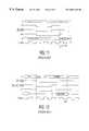
- FIG. 1schematically shows a microcontroller with a memory interface unit which is coupled to a memory.
- FIG. 2is a block diagram of a memory interface unit.
- FIG. 3shows an embodiment of a configuration of a memory interface unit.
- FIG. 4shows special function register addresses of special function memory-mapped registers for use with a memory interface unit.
- FIG. 5shows a set of memory-mapped memory interface unit registers.
- FIG. 6shows bank 0 size and address range selection.
- FIG. 7shows bank 1 - 5 size and base address selection.
- FIG. 8shows a configuration of row/column multiplexer bits for specific DRAMs.
- FIG. 9shows DRAM row and column address multiplexing schemes.
- FIG. 10shows a typical SRAM 16-bit bus read cycle.
- FIG. 11shows a typical SRAM 16-bit bus write cycle.
- FIG. 12shows a typical DRAM 16-bit read cycle.
- FIG. 13shows a typical DRAM 16-bit write cycle.
- FIG. 14shows a DRAM refresh cycle
- FIG. 1schematically shows a microcontroller 1 with a memory interface unit 2 which is coupled to a memory 3 , which comprises a plurality of memory banks of mixed generic and DRAM types.
- the microcontroller 1further comprises a microprocessor 4 , also indicated with CPU, which is coupled to the memory interface unit 2 for controlling the same when executing program code 5 stored in the memory 2 , after a microcontroller reset.
- An address/data/control bus 6is provided between the memory interface unit 2 and the memory 3 .
- a DMA control unit 7which is coupled to the memory interface unit 2 .
- the DMA control unit 7controls a plurality of peripherals (not shown) such as data communication peripherals.
- the CPU (Central Processing Unit) and the DMA (Direct Memory Access) controller 7can request access to the bus 6 , access being granted on the basis of bus arbitration and priority schemes. Such a bus requesting and granting mechanism is well-known in the art.
- active low signalsas indicated in the drawing with a line above a group of characters, are indicated with the symbol — , preceding the group of characters, i.e., if a group of characters ABC indicates an active high logical signal, — ABC indicates the corresponding active low logical signal.
- FIG. 2is a block diagram of the memory interface unit 2 .
- the memory interface unit 2comprises an address selector 20 for selecting a 24 bits CPU address or a 24 bits DMA address on the basis of a granted bus request from the CPU or the DMA controller 6 , respectively, bus requesting and granting being controlled by an arbiter 21 .
- the arbiter 21is further coupled to a DRAM (Dynamic Random Access Memory) refresh timer 22 for also arbitrating DRAM refresh requests, and to a timing generator 23 .
- DRAMDynamic Random Access Memory
- the arbiter 21controls the timing generator 23 which provides timing signals TS to a row/column address generator 24 which generates row and column addresses onto external address pins A 17 -A 6 (i.e., 12 bits) from multiplexed CPU or DMA address bit a 22 -a 0 (i.e, 23 bits) during various DRAM CAS (Column Address Strobe) cycles.
- the timing generator 23further generates global strobe signals to strobe the memory banks included in the memory 3 , such global strobe signals including a byte low enable signal — BLE, a byte high enable signal — BHE, an output enable signal — OE, and a write enable signal — WE.
- An external signal WAITis available after reset.
- a chip select decoder 25is coupled to the address selector 20 .
- up to a maximum of six memory bankscan be selected, six unique programmable strobes — CS 0 , — CS 1 , — CS 2 , — CS 3 , — CS 4 , and — CS 5 being available from the chip select decoder 25 for selecting each memory bank.
- a unique programmable strobeis physically connected to a chip select pin — CS of a generic memory device such as an ROM or SRAM device, or to a — RAS pin of a DRAM device, and is programmed accordingly.
- the chip select decoder 25compares the most significant address bits of all memory addresses to base addresses, i.e., start addresses in a microprocessor memory space, of the maximally memory banks, and asserts the — CS pin for that bank which matches.
- memory bank addressesare on 4 KByte boundary, so a maximum of 12 bits need to be compared only, namely the most significant address bits, indicated by a 23 -a 12 .
- DRAM logical address bits a 22 -a 0are multiplexed onto address pins A 17 -A 6 during the row and column phases by row/column address multiplexing.
- Generic memory logical addresses, a 19 -a 0appear on external address pins A 19 -A 0 directly. Correct read/write bus cycle timing for each bank, programmed in a bank's timing register, is applied via the timing generator 23 whenever the bank is selected.
- the memory interface unit 2uses five special function registers and twenty memory mapped registers, which will be described in the following.
- FIG. 3shows an embodiment of a configuration of the memory interface unit 2 .
- the memory 3has four memory banks, a ROM memory bank 30 of 128K ⁇ 8, i.e., 128 KBytes with a data bus width of 8 bits, indicated by D 7 -D 0 , a DRAM memory bank 31 of 256K ⁇ 16, i.e, 512 KBytes of memory with a data bus width of 16 bits, indicated by D 15 -D 0 , a further DRAM memory bank 32 of 1M ⁇ 16, i.e., 16 MBytes of memory with a data bus of 16 bits, and an SRAM memory bank 33 of 2K ⁇ 16, i.e., 4 KBytes of memory with a data bus width of 16 bits.
- the memory bank 30also being referred to as bank- 0 , comprises program code and starts at a hard wired fixed base address 000000h in the microprocessor's memory space, ‘h’ indicating a hexadecimal address notation.
- the memory interface 2is configured to meet all type, size, base address, width, and timing requirements of the memory banks. Further shown in FIG. 3 are an external address bus ABUS, an external data bus DBUS, and an external control bus CBUS.
- the memory interface chip select signals — CS 0 , — CS 1 , — CS 2 , and — CS 3are connected to the chip select input 34 of the ROM 30 , to the row address strobe input 35 of the DRAM 31 , to the row address strobe input 36 of the DRAM 32 , and to the chip select input 37 of the SRAM 33 , respectively.
- respective column address strobe inputsare shown, indicated by — CASL and — CASH, column address strobe high and low, respectively.
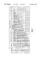
- FIG. 4shows special function register addresses of special function memory-mapped registers used to program the memory interface unit 2 , a bus timing register high BTRH, a bus timing register low BTRL, a memory mapped register base address high MRBH, a memory mapped register base address low BRBL, and a memory interface general configuration register MICFG.
- the register MRBHcontains the high order byte of the MMR base address, address bits A 23 -A 16 , indicated by MA 23 -MA 16 .
- the register MRBLcontains the lowest four bits of the MMR (memory mapped register) base address, address bits A 15 -A 12 , indicated by MA 15 , MA 14 , MA 13 , and MA 12 .
- the LSB(least significant bit) is MRBE, a logic “0” disabling access to the MMRs, and a logic “1” enabling access to the MMRs.
- the MMR base addressis formed by the twelve bits MA 23 -MA 12 , padded by twelve zero bits, and is compared to address bits a 23 -a 12 from the CPU to initiate MMR accesses.
- the register MICFGcontains only one functional bit, the bit CLKOE (Clock Output Enable) which is set at a microprocessor reset.
- FIG. 5shows a set of memory-mapped memory interface unit registers.
- Bits of the BiAM registerhave different functions, depending on a memory bank's type and size.
- the bank's base addressis formed by the bits of the MRBH register and the four MSBs (Most Significant Bits) of the BiAM register
- the six MSBs of the BiAM registerare used as address bits a 23 -a 18 of the base address.
- the two least significant bits of the BiAMare row/column address multiplexer control bits BiMX 1 and BiMX 0 , to be described in more detail in relation to FIG.
- Bits of the BiTMG registerdetermine — CS to — WE delay for generic type memory banks, — RAS to — CAS delay for DRAM memory banks, in clock cycles, and other access timing parameters.
- the MCBL register's MSBenables or disables memory bank- 0 /bank- 1 swapping, bank swapping being disabled upon reset, and further bits determine configuration locking/unlocking of the different memory banks.
- Bits of the RFSH registerenable/disable the refresh timer 22 , and determine a seven-bit time constant for the refresh timer 22 . The timer will time out once every 8 ⁇ RFSH[ 6 : 0 ] system clock cycles, [6:0] indicating the seven LSBs of the RFSH register. On each refresh timer time out, a request is sent to the arbiter 21 .
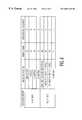
- FIG. 6shows bank- 0 size and address range selection.
- Bank- 0 's base addressis hard wired and is set to 000000h. Shown are bit/settings of the BOCFG register to set the bank's size and address range.
- Bank- 0is the boot bank. Bank- 0 is always enabled for code memory access and can be enabled for data memory access.
- FIG. 7shows bank 1 - 5 size and base address selection.
- Bank- 1 to bank- 5 size and address selectionis determined by bit settings of the BiCFG register, the NMR register, and the BiAM register, as shown, lower address bits being zero, as the case may be.
- Banks bank- 1 to bank- 5can be configured as either a generic memory or a DRAM.
- application code stored in bank- 0a ROM
- bank- 1preferably a DRAM memory bank
- the application codecan still be accessed from base address 000000h.
- Bank swappingalso allows interrupt vectors, which are in low memory, to be write accessed. The advantage of such a bank swapping is that the application code is executed substantially faster.
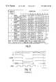
- FIG. 8shows a configuration of row/column multiplexer bits for specific DRAMs.
- the two least significant bits of the BiAM register, the row/column address multiplexer control bits BiMX 1 and BiMX 0determine multiplex scheme A through G for various data bus width and memory sizes.
- FIG. 9shows the DRAM row and column address multiplexing schemes A through G in relation to the assignment of logical addresses a 23 -a 0 to the external pins A 17 -A 6 during the row and column address phases of a DRAM access, ‘u’ indicating unused pins.
- so-called — CAS before — RAS refreshis performed.
- Bank 30the boot bank, and bank 31 , the first DRAM bank, are first configured after a reset.
- Bank 30has address range 000000h-01FFFFh as indicated by the register B 0 CFG described in FIG. 6 .
- Bank 31has address range 100000h-17FFFFh as indicated by the registers B 1 CFG, MRB, and B 1 AM described in FIG. 7 .
- sizes and ranges of banks 32 and 33are indicated.
- the address ranges and sizes of bank 30 and bank 31are interchanged, the then address range of bank 31 , 10000h-11FFFFh activating the ROM on CSO, and the then address range 000000h-07ffffh activating the DRAM on — CS 1 .
- the banksare configured as follows.
- the MRBH registeris set to FFh, indicating M base address bits a 23 - 16 .
- the MRBL registeris set to F1h, bits [3:1] of the MRBL register being don't cares, and MMR access is enabled.
- the MCBL registeris set to lock the registers for banks 4 and 5 , which are not present, and to unlock the registers for banks 3 - 0 .
- bank 30is data access disabled.
- Bank 31is set to two cycle — RAS to — CAS delay, and to two cycle delay from data strobes low to sampling of the data bus or latching data into memory, by appropriate settings of the B 1 TMG register.
- the B 1 CFG registeris set to code and data enable the memory bank 31 and to indicate a DRAM type memory of size 512 KBytes of 16 bit words.
- the B 1 AM registeris set to 10h, indicating a bank 31 base address 100000h and indicating multiplexing scheme E as described in FIGS. 8 and 9.
- Banks 32 and 33are configured correspondingly.
- the refresh timing register RFSHis configured.
- the two DRAMs 31 and 32have the same refresh cycle timing requirement. If they were different, the shortest cycle would be chosen.
- the application code, and any other datais moved from the ROM 30 to the DRAM 31 . Then, bank swapping is performed.
- FIGS. 10-13illustrate the effects of memory interface settings, particularly the effects of the settings of the register BiTMG.
- FIG. 10shows a typical SRAM 16-bit bus read cycle in accordance with a preferred embodiment of the present invention.
- Access timeis set to 2 clock cycles.
- the addressis driven onto the address bus ABUS.
- — BLE/ — BHEgo active on the same cycle.
- the data bus DBUSis sampled on the rising edge of ClkOut, 2 cycles later.
- the read cycleis terminated as — CS, — BLE/ — BLH, and — OE are negated, and the address buss ABUS and the data bus DBUS begin to change
- FIG. 11shows a typical SRAM 16-bit bus write cycle in accordance with a preferred embodiment of the present invention.
- the addressis driven onto the address bus ABUS.
- CSgoes active.
- BLE/ — BHEgo active on the same cycle.
- the dataare driven onto the data bus DBUS.
- — CSis also negated on this cycle.
- One clock cycle later, — WEis negated, terminating the write cycle, and the address bus ABUS and the data bus DBUS change.
- a — BLE/ — BHE bus strobeacts as a data strobe.
- FIG. 12shows a typical DRAM 16-bit read cycle in accordance with a preferred embodiment of the present invention.
- the RAS to — CAS delayis set to two clock cycles.
- the row addressis multiplexed onto pins A 17 -A 6 .
- — CS( — RAS) and — OEgo active.
- the column addressis multiplexed onto the address bus.
- Two clock cycles after — RAS, — BLE/ — BHEgo active.
- the DRAMdrives the data onto the data bus.
- — BLE/ — BHE— CAS
- the data busis sampled on the rising edge of — BLE/ — BHE, — OE is also negated, and the address bus changes.
- the — BLE/ — BHE bus strobeacts as a — CAS strobe.
- FIG. 13shows a typical DRAM 16-bit write cycle in accordance with a preferred embodiment of the present invention.
- the register BTMGis set to an access time of two clock cycles.
- the row addressis multiplexed onto the pins A 17 -A 6 .
- — CS ( — RAS) and — WEgo active, and the data are driven onto the data bus.
- CS ( — RAS)One clock cycle after — CS ( — RAS)
- the column addressis multiplexed onto the address bus.
- FIG. 14shows a DRAM refresh cycle.
- a — CS ( — RAS)is asserted for all memory banks configured for DRAMs.
- the — CS ( — RAS) and — BLE/ — BHE( — CAS)are negated.
- a recovery time RTis four clock cycles.
- the shown DRAM refresh cycleis a so-called — CAS before — RAS refresh cycle, in which the unique — CS( — RAS) strobe and global bus strobe — BLE/ — BHE( — CAS) cooperate to perform the refresh cycle.
- a column in the DRAMwill be refreshed.
Landscapes
- Engineering & Computer Science (AREA)
- Theoretical Computer Science (AREA)
- Physics & Mathematics (AREA)
- General Engineering & Computer Science (AREA)
- General Physics & Mathematics (AREA)
- Microelectronics & Electronic Packaging (AREA)
- Dram (AREA)
- Microcomputers (AREA)
Abstract
Description
Claims (19)
Priority Applications (6)
| Application Number | Priority Date | Filing Date | Title |
|---|---|---|---|
| US09/198,925US6601130B1 (en) | 1998-11-24 | 1998-11-24 | Memory interface unit with programmable strobes to select different memory devices |
| KR1020007008064AKR100679758B1 (en) | 1998-11-24 | 1999-11-03 | Memory Interface Units and Data Processor Integrated Circuits Including the Same |
| PCT/EP1999/008614WO2000031646A2 (en) | 1998-11-24 | 1999-11-03 | Data processor integrated circuit with a memory interface unit with programmable strobes to select different memory devices |
| DE69940397TDE69940397D1 (en) | 1998-11-24 | 1999-11-03 | DATA PROCESSOR INTEGRATED CIRCUIT WITH MEMORY INTERFACE UNIT WITH PROGRAMMABLE PULSE FOR THE SELECTION OF DIFFERENT MEMORY DEVICES |
| EP99964480AEP1055178B1 (en) | 1998-11-24 | 1999-11-03 | Data processor integrated circuit with a memory interface unit with programmable strobes to select different memory devices |
| JP2000584395AJP2002530777A (en) | 1998-11-24 | 1999-11-03 | Data processing integrated circuit having a memory interface unit with a programmable strobe for selecting different memory devices |
Applications Claiming Priority (1)
| Application Number | Priority Date | Filing Date | Title |
|---|---|---|---|
| US09/198,925US6601130B1 (en) | 1998-11-24 | 1998-11-24 | Memory interface unit with programmable strobes to select different memory devices |
Publications (1)
| Publication Number | Publication Date |
|---|---|
| US6601130B1true US6601130B1 (en) | 2003-07-29 |
Family
ID=22735474
Family Applications (1)
| Application Number | Title | Priority Date | Filing Date |
|---|---|---|---|
| US09/198,925Expired - LifetimeUS6601130B1 (en) | 1998-11-24 | 1998-11-24 | Memory interface unit with programmable strobes to select different memory devices |
Country Status (6)
| Country | Link |
|---|---|
| US (1) | US6601130B1 (en) |
| EP (1) | EP1055178B1 (en) |
| JP (1) | JP2002530777A (en) |
| KR (1) | KR100679758B1 (en) |
| DE (1) | DE69940397D1 (en) |
| WO (1) | WO2000031646A2 (en) |
Cited By (20)
| Publication number | Priority date | Publication date | Assignee | Title |
|---|---|---|---|---|
| US20010056521A1 (en)* | 2000-04-06 | 2001-12-27 | Hirokatsu Fujiwara | Information processing system with memory element performance-dependent memory control |
| US20040064667A1 (en)* | 2002-09-26 | 2004-04-01 | Analog Devices, Inc. | Method and system for providing a contiguous memory address space |
| US20040122984A1 (en)* | 2001-05-14 | 2004-06-24 | Hidemi Oyama | Data processor and data table update method |
| US20040143696A1 (en)* | 2003-01-21 | 2004-07-22 | Francis Hsieh | Data storage system for fast booting of computer |
| US6792499B1 (en)* | 2000-11-14 | 2004-09-14 | Cypress Semiconductor Corp. | Dynamic swapping of memory bank base addresses |
| US20050041453A1 (en)* | 2003-08-22 | 2005-02-24 | Brazis Paul W. | Method and apparatus for reading and writing to solid-state memory |
| US6876563B1 (en)* | 2002-12-20 | 2005-04-05 | Cypress Semiconductor Corporation | Method for configuring chip selects in memories |
| US20070242551A1 (en)* | 2002-02-11 | 2007-10-18 | Micron Technology, Inc. | User selectable banks for DRAM |
| US20080008023A1 (en)* | 2006-07-05 | 2008-01-10 | Martin Brox | Memory device, and method for operating a memory device |
| US7711907B1 (en) | 2007-02-14 | 2010-05-04 | Xilinx, Inc. | Self aligning state machine |
| US7720636B1 (en) | 2007-02-14 | 2010-05-18 | Xilinx, Inc. | Performance monitors (PMs) for measuring performance in a system and providing a record of transactions performed |
| US20100180099A1 (en)* | 2009-01-09 | 2010-07-15 | Via Technologies, Inc. | Apparatus, system and method for prefetching data in bus system |
| US7913022B1 (en)* | 2007-02-14 | 2011-03-22 | Xilinx, Inc. | Port interface modules (PIMs) in a multi-port memory controller (MPMC) |
| US8479124B1 (en) | 2007-02-14 | 2013-07-02 | Xilinx, Inc. | Graphical user interface (GUI) including input files with information that determines representation of subsequent content displayed by the GUI |
| US20130176768A1 (en)* | 2011-09-16 | 2013-07-11 | Inphi Corporation | Replacement of a faulty memory cell with a spare cell for a memory circuit |
| US9069717B1 (en) | 2012-03-06 | 2015-06-30 | Inphi Corporation | Memory parametric improvements |
| US9158726B2 (en) | 2011-12-16 | 2015-10-13 | Inphi Corporation | Self terminated dynamic random access memory |
| US10452561B2 (en) | 2016-08-08 | 2019-10-22 | Raytheon Company | Central processing unit architecture and methods for high availability systems |
| CN111951842A (en)* | 2019-05-15 | 2020-11-17 | 瑞昱半导体股份有限公司 | Method and memory controller for simultaneous access to dynamic random access memory |
| US20230061878A1 (en)* | 2021-09-01 | 2023-03-02 | Dell Products L.P. | Memory architecture having ranks with variable data widths |
Citations (12)
| Publication number | Priority date | Publication date | Assignee | Title |
|---|---|---|---|---|
| US4028682A (en) | 1973-12-22 | 1977-06-07 | Olympia Werke Ag | Circuit arrangement for selecting the function of connection contacts on circuit chips |
| US4349870A (en) | 1979-09-05 | 1982-09-14 | Motorola, Inc. | Microcomputer with programmable multi-function port |
| US4903197A (en)* | 1987-02-27 | 1990-02-20 | Bull Hn Information Systems Inc. | Memory bank selection arrangement generating first bits identifying a bank of memory and second bits addressing identified bank |
| US5261116A (en) | 1986-07-02 | 1993-11-09 | Advanced Micro Devices, Inc. | Programmable, expandable controller with flexible I/O |
| GB2271003A (en) | 1992-09-23 | 1994-03-30 | Intel Corp | High integration DRAM controller |
| US5598372A (en)* | 1994-07-27 | 1997-01-28 | Hitachi, Ltd. | Semiconductor memory |
| JPH09180431A (en) | 1995-12-26 | 1997-07-11 | Nec Niigata Ltd | Single in-line memory module system |
| US5715207A (en) | 1996-03-28 | 1998-02-03 | International Business Machines Corporation | Memory presence and type detection using multiplexed memory line function |
| US5761478A (en) | 1994-12-12 | 1998-06-02 | Texas Instruments Incorporated | Programmable memory interface for efficient transfer of different size data |
| US5781492A (en)* | 1997-02-04 | 1998-07-14 | Advanced Micro Devices, Inc. | System and method for mapping memory to DRAM after system boot from non-volatile memory |
| US5966727A (en)* | 1996-07-12 | 1999-10-12 | Dux Inc. | Combination flash memory and dram memory board interleave-bypass memory access method, and memory access device incorporating both the same |
| US6023750A (en)* | 1997-03-07 | 2000-02-08 | Advanced Micro Devices, Inc. | Microcontroller having dedicated hardware for memory address space expansion via auxilliary address signal generation |
Family Cites Families (1)
| Publication number | Priority date | Publication date | Assignee | Title |
|---|---|---|---|---|
| KR100252254B1 (en)* | 1996-06-26 | 2000-04-15 | 윤종용 | Interoperable computer system of heterogeneous memory modules |
- 1998
- 1998-11-24USUS09/198,925patent/US6601130B1/ennot_activeExpired - Lifetime
- 1999
- 1999-11-03KRKR1020007008064Apatent/KR100679758B1/ennot_activeExpired - Fee Related
- 1999-11-03JPJP2000584395Apatent/JP2002530777A/ennot_activeWithdrawn
- 1999-11-03EPEP99964480Apatent/EP1055178B1/ennot_activeExpired - Lifetime
- 1999-11-03WOPCT/EP1999/008614patent/WO2000031646A2/enactiveIP Right Grant
- 1999-11-03DEDE69940397Tpatent/DE69940397D1/ennot_activeExpired - Lifetime
Patent Citations (12)
| Publication number | Priority date | Publication date | Assignee | Title |
|---|---|---|---|---|
| US4028682A (en) | 1973-12-22 | 1977-06-07 | Olympia Werke Ag | Circuit arrangement for selecting the function of connection contacts on circuit chips |
| US4349870A (en) | 1979-09-05 | 1982-09-14 | Motorola, Inc. | Microcomputer with programmable multi-function port |
| US5261116A (en) | 1986-07-02 | 1993-11-09 | Advanced Micro Devices, Inc. | Programmable, expandable controller with flexible I/O |
| US4903197A (en)* | 1987-02-27 | 1990-02-20 | Bull Hn Information Systems Inc. | Memory bank selection arrangement generating first bits identifying a bank of memory and second bits addressing identified bank |
| GB2271003A (en) | 1992-09-23 | 1994-03-30 | Intel Corp | High integration DRAM controller |
| US5598372A (en)* | 1994-07-27 | 1997-01-28 | Hitachi, Ltd. | Semiconductor memory |
| US5761478A (en) | 1994-12-12 | 1998-06-02 | Texas Instruments Incorporated | Programmable memory interface for efficient transfer of different size data |
| JPH09180431A (en) | 1995-12-26 | 1997-07-11 | Nec Niigata Ltd | Single in-line memory module system |
| US5715207A (en) | 1996-03-28 | 1998-02-03 | International Business Machines Corporation | Memory presence and type detection using multiplexed memory line function |
| US5966727A (en)* | 1996-07-12 | 1999-10-12 | Dux Inc. | Combination flash memory and dram memory board interleave-bypass memory access method, and memory access device incorporating both the same |
| US5781492A (en)* | 1997-02-04 | 1998-07-14 | Advanced Micro Devices, Inc. | System and method for mapping memory to DRAM after system boot from non-volatile memory |
| US6023750A (en)* | 1997-03-07 | 2000-02-08 | Advanced Micro Devices, Inc. | Microcontroller having dedicated hardware for memory address space expansion via auxilliary address signal generation |
Cited By (30)
| Publication number | Priority date | Publication date | Assignee | Title |
|---|---|---|---|---|
| US20010056521A1 (en)* | 2000-04-06 | 2001-12-27 | Hirokatsu Fujiwara | Information processing system with memory element performance-dependent memory control |
| US6877078B2 (en)* | 2000-04-06 | 2005-04-05 | Hitachi, Ltd. | Information processing system with memory element performance-dependent memory control |
| US6792499B1 (en)* | 2000-11-14 | 2004-09-14 | Cypress Semiconductor Corp. | Dynamic swapping of memory bank base addresses |
| US20040122984A1 (en)* | 2001-05-14 | 2004-06-24 | Hidemi Oyama | Data processor and data table update method |
| US20070242551A1 (en)* | 2002-02-11 | 2007-10-18 | Micron Technology, Inc. | User selectable banks for DRAM |
| US7995420B2 (en) | 2002-02-11 | 2011-08-09 | Round Rock Research, Llc | User selectable banks for DRAM |
| US7636271B2 (en)* | 2002-02-11 | 2009-12-22 | Micron Technology, Inc. | User selectable banks for DRAM |
| US20100097878A1 (en)* | 2002-02-11 | 2010-04-22 | Micron Technology, Inc. | User selectable banks for dram |
| US6981122B2 (en)* | 2002-09-26 | 2005-12-27 | Analog Devices, Inc. | Method and system for providing a contiguous memory address space |
| US20040064667A1 (en)* | 2002-09-26 | 2004-04-01 | Analog Devices, Inc. | Method and system for providing a contiguous memory address space |
| US6876563B1 (en)* | 2002-12-20 | 2005-04-05 | Cypress Semiconductor Corporation | Method for configuring chip selects in memories |
| US20040143696A1 (en)* | 2003-01-21 | 2004-07-22 | Francis Hsieh | Data storage system for fast booting of computer |
| US20050041453A1 (en)* | 2003-08-22 | 2005-02-24 | Brazis Paul W. | Method and apparatus for reading and writing to solid-state memory |
| US20080008023A1 (en)* | 2006-07-05 | 2008-01-10 | Martin Brox | Memory device, and method for operating a memory device |
| US7564735B2 (en) | 2006-07-05 | 2009-07-21 | Qimonda Ag | Memory device, and method for operating a memory device |
| US7711907B1 (en) | 2007-02-14 | 2010-05-04 | Xilinx, Inc. | Self aligning state machine |
| US7913022B1 (en)* | 2007-02-14 | 2011-03-22 | Xilinx, Inc. | Port interface modules (PIMs) in a multi-port memory controller (MPMC) |
| US7720636B1 (en) | 2007-02-14 | 2010-05-18 | Xilinx, Inc. | Performance monitors (PMs) for measuring performance in a system and providing a record of transactions performed |
| US8479124B1 (en) | 2007-02-14 | 2013-07-02 | Xilinx, Inc. | Graphical user interface (GUI) including input files with information that determines representation of subsequent content displayed by the GUI |
| US20100180099A1 (en)* | 2009-01-09 | 2010-07-15 | Via Technologies, Inc. | Apparatus, system and method for prefetching data in bus system |
| US8127108B2 (en)* | 2009-01-09 | 2012-02-28 | Via Technologies, Inc. | Apparatus, system and method for prefetching data in bus system |
| US8971094B2 (en)* | 2011-09-16 | 2015-03-03 | Inphi Corporation | Replacement of a faulty memory cell with a spare cell for a memory circuit |
| US20130176768A1 (en)* | 2011-09-16 | 2013-07-11 | Inphi Corporation | Replacement of a faulty memory cell with a spare cell for a memory circuit |
| US9158726B2 (en) | 2011-12-16 | 2015-10-13 | Inphi Corporation | Self terminated dynamic random access memory |
| US9069717B1 (en) | 2012-03-06 | 2015-06-30 | Inphi Corporation | Memory parametric improvements |
| US9230635B1 (en) | 2012-03-06 | 2016-01-05 | Inphi Corporation | Memory parametric improvements |
| US10452561B2 (en) | 2016-08-08 | 2019-10-22 | Raytheon Company | Central processing unit architecture and methods for high availability systems |
| CN111951842A (en)* | 2019-05-15 | 2020-11-17 | 瑞昱半导体股份有限公司 | Method and memory controller for simultaneous access to dynamic random access memory |
| US20230061878A1 (en)* | 2021-09-01 | 2023-03-02 | Dell Products L.P. | Memory architecture having ranks with variable data widths |
| US11798604B2 (en)* | 2021-09-01 | 2023-10-24 | Dell Products L.P. | Memory architecture having ranks with variable data widths |
Also Published As
| Publication number | Publication date |
|---|---|
| WO2000031646A2 (en) | 2000-06-02 |
| EP1055178B1 (en) | 2009-02-11 |
| WO2000031646A3 (en) | 2000-10-05 |
| KR20010034334A (en) | 2001-04-25 |
| DE69940397D1 (en) | 2009-03-26 |
| EP1055178A2 (en) | 2000-11-29 |
| JP2002530777A (en) | 2002-09-17 |
| KR100679758B1 (en) | 2007-02-07 |
Similar Documents
| Publication | Publication Date | Title |
|---|---|---|
| US6601130B1 (en) | Memory interface unit with programmable strobes to select different memory devices | |
| US10403333B2 (en) | Memory controller with flexible address decoding | |
| US5301278A (en) | Flexible dynamic memory controller | |
| US7120754B2 (en) | Synchronous DRAM with selectable internal prefetch size | |
| KR100265263B1 (en) | Programmable shared memory system and method | |
| US5729709A (en) | Memory controller with burst addressing circuit | |
| KR100244841B1 (en) | High-speed, multiple-port, interleaved cache with arbitration of multiple access addresses | |
| EP0444601B1 (en) | Data processor with interleaved DRAM memory | |
| US5226134A (en) | Data processing system including a memory controller for direct or interleave memory accessing | |
| US5509138A (en) | Method for determining speeds of memory modules | |
| JPH04230544A (en) | Data processing apparatus for dynamically setting timing of dynamic memory system | |
| CN107257964B (en) | DRAM circuit, computer system and method for accessing DRAM circuit | |
| US5987581A (en) | Configurable address line inverter for remapping memory | |
| US5210847A (en) | Noncacheable address random access memory | |
| US5586300A (en) | Flexible addressing memory controller wherein multiple memory modules may be accessed according to comparison of configuration addresses | |
| US5901298A (en) | Method for utilizing a single multiplex address bus between DRAM, SRAM and ROM | |
| US7398362B1 (en) | Programmable interleaving in multiple-bank memories | |
| KR100298955B1 (en) | Data processing system | |
| US5740382A (en) | Method and apparatus for accessing a chip-selectable device in a data processing system | |
| KR100452325B1 (en) | AMBA-based Multiprocessor system for processor identification number allocation and sequential booting | |
| US5748922A (en) | Method and apparatus for reading data from a write only port | |
| JP2004078396A (en) | Memory device | |
| JP3600830B2 (en) | Processor | |
| JPH05274868A (en) | Memory control device | |
| JPH0371483A (en) | memory access control device |
Legal Events
| Date | Code | Title | Description |
|---|---|---|---|
| AS | Assignment | Owner name:PHILIPS ELECTRONICS NORTH AMERICA CORPORATION, NEW Free format text:ASSIGNMENT OF ASSIGNORS INTEREST;ASSIGNORS:SLIVKOFF, WILLIAM J.;LEE, FRANK S.;KOLB, WILLIAM W.;REEL/FRAME:009718/0777 Effective date:19990111 | |
| AS | Assignment | Owner name:KONINKLIJKE PHILIPS ELECTRONICS N.V., NETHERLANDS Free format text:ASSIGNMENT OF ASSIGNORS INTEREST;ASSIGNOR:PHILIPS ELECTRONICS NORTH AMERICA CORP.;REEL/FRAME:013651/0538 Effective date:20030503 | |
| STCF | Information on status: patent grant | Free format text:PATENTED CASE | |
| FPAY | Fee payment | Year of fee payment:4 | |
| AS | Assignment | Owner name:NXP B.V., NETHERLANDS Free format text:ASSIGNMENT OF ASSIGNORS INTEREST;ASSIGNOR:PHILIPS ELECTRONICS NORTH AMERICA CORP.;REEL/FRAME:018654/0521 Effective date:20061213 | |
| FPAY | Fee payment | Year of fee payment:8 | |
| AS | Assignment | Owner name:NXP B.V., NETHERLANDS Free format text:NUNC PRO TUNC ASSIGNMENT;ASSIGNOR:KONINKLIJKE PHILIPS ELECTRONICS N.V.;REEL/FRAME:028406/0748 Effective date:20120620 | |
| AS | Assignment | Owner name:PARTNERS FOR CORPORATE RESEARCH INTERNATIONAL, CAY Free format text:ASSIGNMENT OF ASSIGNORS INTEREST;ASSIGNOR:NXP B. V.;REEL/FRAME:031334/0449 Effective date:20120907 | |
| AS | Assignment | Owner name:FUTURE LINK SYSTEMS, CALIFORNIA Free format text:ASSIGNMENT OF ASSIGNORS INTEREST;ASSIGNOR:PARTNERS FOR CORPORATE RESEARCH INTERNATIONAL;REEL/FRAME:032399/0965 Effective date:20130808 | |
| FPAY | Fee payment | Year of fee payment:12 |