US6600591B2 - Micromirror array having adjustable mirror angles - Google Patents
Micromirror array having adjustable mirror anglesDownload PDFInfo
- Publication number
- US6600591B2 US6600591B2US09/880,230US88023001AUS6600591B2US 6600591 B2US6600591 B2US 6600591B2US 88023001 AUS88023001 AUS 88023001AUS 6600591 B2US6600591 B2US 6600591B2
- Authority
- US
- United States
- Prior art keywords
- voltage
- optical
- micromirror
- electrode
- micromirrors
- Prior art date
- Legal status (The legal status is an assumption and is not a legal conclusion. Google has not performed a legal analysis and makes no representation as to the accuracy of the status listed.)
- Expired - Lifetime, expires
Links
- 230000003287optical effectEffects0.000claimsabstractdescription82
- 238000000034methodMethods0.000claimsabstractdescription30
- 239000000758substrateSubstances0.000claimsdescription22
- 230000003595spectral effectEffects0.000claimsdescription19
- 238000004891communicationMethods0.000claimsdescription11
- 230000004044responseEffects0.000claimsdescription6
- 230000007246mechanismEffects0.000claimsdescription3
- 230000008859changeEffects0.000claimsdescription2
- 238000003491arrayMethods0.000description10
- 230000006870functionEffects0.000description10
- 238000000926separation methodMethods0.000description7
- 230000006399behaviorEffects0.000description4
- 238000012937correctionMethods0.000description3
- 230000000694effectsEffects0.000description3
- 239000000835fiberSubstances0.000description3
- 230000008569processEffects0.000description3
- 238000009825accumulationMethods0.000description2
- 230000008901benefitEffects0.000description2
- 238000010276constructionMethods0.000description2
- 238000013461designMethods0.000description2
- 238000010586diagramMethods0.000description2
- 230000009977dual effectEffects0.000description2
- 238000004519manufacturing processMethods0.000description2
- 239000013307optical fiberSubstances0.000description2
- 230000000135prohibitive effectEffects0.000description2
- 230000002441reversible effectEffects0.000description2
- 238000007789sealingMethods0.000description2
- 230000003068static effectEffects0.000description2
- 239000004593EpoxySubstances0.000description1
- 230000009471actionEffects0.000description1
- 238000005452bendingMethods0.000description1
- 230000015556catabolic processEffects0.000description1
- 125000004122cyclic groupChemical group0.000description1
- 230000007423decreaseEffects0.000description1
- 238000006731degradation reactionMethods0.000description1
- 238000001514detection methodMethods0.000description1
- 238000011161developmentMethods0.000description1
- 238000006073displacement reactionMethods0.000description1
- 230000005059dormancyEffects0.000description1
- 238000005421electrostatic potentialMethods0.000description1
- 238000005516engineering processMethods0.000description1
- 239000011521glassSubstances0.000description1
- 230000006872improvementEffects0.000description1
- 230000000670limiting effectEffects0.000description1
- 238000012986modificationMethods0.000description1
- 230000004048modificationEffects0.000description1
- 230000006855networkingEffects0.000description1
- 238000004806packaging method and processMethods0.000description1
- 230000009467reductionEffects0.000description1
- 230000002829reductive effectEffects0.000description1
- 230000035945sensitivityEffects0.000description1
- 239000007787solidSubstances0.000description1
- 238000012360testing methodMethods0.000description1
- 238000011144upstream manufacturingMethods0.000description1
Images


Classifications
- G—PHYSICS
- G02—OPTICS
- G02B—OPTICAL ELEMENTS, SYSTEMS OR APPARATUS
- G02B26/00—Optical devices or arrangements for the control of light using movable or deformable optical elements
- G02B26/08—Optical devices or arrangements for the control of light using movable or deformable optical elements for controlling the direction of light
- G02B26/0816—Optical devices or arrangements for the control of light using movable or deformable optical elements for controlling the direction of light by means of one or more reflecting elements
- G02B26/0833—Optical devices or arrangements for the control of light using movable or deformable optical elements for controlling the direction of light by means of one or more reflecting elements the reflecting element being a micromechanical device, e.g. a MEMS mirror, DMD
- G02B26/0841—Optical devices or arrangements for the control of light using movable or deformable optical elements for controlling the direction of light by means of one or more reflecting elements the reflecting element being a micromechanical device, e.g. a MEMS mirror, DMD the reflecting element being moved or deformed by electrostatic means
- Y—GENERAL TAGGING OF NEW TECHNOLOGICAL DEVELOPMENTS; GENERAL TAGGING OF CROSS-SECTIONAL TECHNOLOGIES SPANNING OVER SEVERAL SECTIONS OF THE IPC; TECHNICAL SUBJECTS COVERED BY FORMER USPC CROSS-REFERENCE ART COLLECTIONS [XRACs] AND DIGESTS
- Y10—TECHNICAL SUBJECTS COVERED BY FORMER USPC
- Y10S—TECHNICAL SUBJECTS COVERED BY FORMER USPC CROSS-REFERENCE ART COLLECTIONS [XRACs] AND DIGESTS
- Y10S359/00—Optical: systems and elements
- Y10S359/904—Micromirror
Definitions
- Embodiments of the inventionare thus directed to a method and system that permits individual tilt angles to be selected for optical micromirrors within an array.
- Each optical micromirror in the arrayincludes a structural film connected with a substrate by a structural linkage.
- At least one electrodeis configured to tilt the structural film upon application of a voltage.
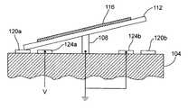
- each micromirroris configured as shown in FIGS. 1A-1C, perhaps without the hard stops 120 a and 120 b .
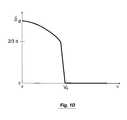
- FIG. 1Dis shown graphically the dependence of the separation ⁇ between the micromirror structural film 112 and the substrate 104 on the side of the structural linkage 108 where a potential is applied to actuator 124 a or 124 b .
- Va voltage
- V 0the snap-in voltage
- embodiments of the inventionuse an arrangement that exploits the slow discharge response of the electrodes.
- a cyclic procedureis used in which the desired voltage for each electrode is applied for a short period of time, typically less than 1 ms, with a voltage being applied to each electrode sequentially throughout the entire array. For an array with N ⁇ 100, this results in every electrode having a voltage applied to it at least several times every second.
- the micromirror statesare thus held without contact that may lead to stiction concerns, and with the added advantage that the tilt of each micromirror may be defined individually.
- FIG. 4shows schematically how components of such a system may be interconnected and FIG. 5 illustrates the steps used by those components to maintain the appropriate tilts.
- the systemincludes a controller 408 that is in communication with a digital memory 404 , a digital-analog converter 412 , and a multichannel digital driver 416 .
- the digital memorymay comprise an (electrically) erasable programmable read-only memory (EPROM or EEPROM).
- the digital driver 416is a three-state driver capable of handling at least 2N channels.
- the digital driver 416is connected with the electrode array 420 so that each electrode is configured for communication with a separate channel.
- the digital-analog converter 412may be configured to have a narrow adjust range with an adder high-voltage offset.
- the time tis preferably short but still sufficiently long to ensure that the micromirror is maintained in the unswitched state. Typically a time on an order less than milliseconds is appropriate.
- the driveris turned off at step 540 and put back into high-impedance mode.
- FIGS. 7A and 7BAnother embodiment of a wavelength router, designated 10 ′, is illustrated with schematic top and side views in FIGS. 7A and 7B, respectively. This embodiment may be considered an unfolded version of the embodiment of FIGS. 6A-6C.
- Light entering the wavelength router 10 ′ from input port 12forms diverging beam 18 , which includes the different spectral bands. Beam 18 encounters a first lens 20 a , which collimates the light and directs it to a transmissive grating 25 ′.
- the grating 25 ′disperses the light so that collimated beams at different wavelengths encounter a second lens 20 b , which focuses the beams.
- the focused beamsare reflected by respective ones of plurality of retroreflectors 30 , which may also be configured as contactless micromirror optical switches, as diverging beams, back to lens 20 b , which collimates them and directs them to grating 25 ′.
- the grating 25 ′removes the angular separation between the different beams, which are then focused in the plane of output ports 15 by lens 20 a.
- micromirror 65in a first orientation so as to direct the incoming beam to micromirror 66 ( 1 ), which is oriented 90° with respect to micromirror 65 's first orientation to direct the beam back in a direction opposite to the incident direction.
- the right half of the figureshows micromirror 65 in a second orientation so as to direct the incident beam to micromirror 66 (M).
- micromirror 65is moved to select the output position of the beam, while micromirrors 66 ( 1 . . . M) are fixed during normal operation.
- Micromirror 65 and the row of micromirrors 66 ( 1 . . . M)can be replicated and displaced in a direction perpendicular to the plane of the figure. While micromirror array 62 need only be one-dimensional, it may be convenient to provide additional micromirrors to provide additional flexibility.
- embodiments of the inventionpermit an improvement in dual-level MEMS switching.
- dual-level switching configurationsuse two operational voltages.
- a first, higher, voltage V sis used to perform switching of the micromirror from one tilt position to another.
- a second, lower, voltage V his used to maintain the position of the micromirror.
Landscapes
- Physics & Mathematics (AREA)
- General Physics & Mathematics (AREA)
- Optics & Photonics (AREA)
- Mechanical Light Control Or Optical Switches (AREA)
Abstract
Description
Claims (35)
Priority Applications (1)
| Application Number | Priority Date | Filing Date | Title |
|---|---|---|---|
| US09/880,230US6600591B2 (en) | 2001-06-12 | 2001-06-12 | Micromirror array having adjustable mirror angles |
Applications Claiming Priority (1)
| Application Number | Priority Date | Filing Date | Title |
|---|---|---|---|
| US09/880,230US6600591B2 (en) | 2001-06-12 | 2001-06-12 | Micromirror array having adjustable mirror angles |
Publications (2)
| Publication Number | Publication Date |
|---|---|
| US20020186449A1 US20020186449A1 (en) | 2002-12-12 |
| US6600591B2true US6600591B2 (en) | 2003-07-29 |
Family
ID=25375793
Family Applications (1)
| Application Number | Title | Priority Date | Filing Date |
|---|---|---|---|
| US09/880,230Expired - LifetimeUS6600591B2 (en) | 2001-06-12 | 2001-06-12 | Micromirror array having adjustable mirror angles |
Country Status (1)
| Country | Link |
|---|---|
| US (1) | US6600591B2 (en) |
Cited By (48)
| Publication number | Priority date | Publication date | Assignee | Title |
|---|---|---|---|---|
| US20020197002A1 (en)* | 2001-06-25 | 2002-12-26 | Chuang-Chia Lin | Self assembled micro anti-stiction structure |
| US20030081308A1 (en)* | 2001-08-20 | 2003-05-01 | So John Ling Wing | Optical system and method |
| US20030117687A1 (en)* | 2001-12-21 | 2003-06-26 | Olympus Optical Co., Ltd. | Optical deflector and optical deflector array |
| US20030202738A1 (en)* | 2002-04-30 | 2003-10-30 | Xerox Corporation | Optical switching system |
| US20030202735A1 (en)* | 2002-04-30 | 2003-10-30 | Xerox Corporation | Electrode design and positioning for controlled movement of a moveable electrode and associated support structure |
| US20040008926A1 (en)* | 2002-06-20 | 2004-01-15 | Walsin Lihwa Corp. | Micromirror switch and transmission method thereof |
| US20040061414A1 (en)* | 2002-09-30 | 2004-04-01 | Greywall Dennis S. | Split spring for MEMS devices |
| US20040061923A1 (en)* | 2002-09-30 | 2004-04-01 | Greywall Dennis S. | Monolithic two-axis MEMS device for optical switches |
| US20040061924A1 (en)* | 2002-09-30 | 2004-04-01 | Greywall Dennis S. | Monolithic MEMS device for optical switches |
| US20050099670A1 (en)* | 2003-10-16 | 2005-05-12 | Fuji Photo Film Co., Ltd. | Reflection-type light modulating array element and exposure apparatus |
| US20050231204A1 (en)* | 2004-04-17 | 2005-10-20 | Martin Eric T | Testing MEM device array |
| US20060049826A1 (en)* | 2001-03-01 | 2006-03-09 | Onix Microsystems | Optical cross-connect system |
| US20060066423A1 (en)* | 2004-09-29 | 2006-03-30 | Greywall Dennis S | Monolithic MEMS device having a balanced cantilever plate |
| US20060103908A1 (en)* | 2004-11-12 | 2006-05-18 | Asml Holding N.V. | Active faceted mirror system for lithography |
| US7072090B2 (en)* | 2004-04-22 | 2006-07-04 | Micronic Laser Systems Ab | Addressing of an SLM |
| US20060187517A1 (en)* | 2002-03-15 | 2006-08-24 | Micronic Laser Systems Ab | Addressing method of movable elements in a spatial light modulator (SLM) |
| US20060214534A1 (en)* | 2005-03-28 | 2006-09-28 | Maurice Thomas | Versatile digitally controlled micro-mechanical actuator |
| US20070229821A1 (en)* | 2006-04-04 | 2007-10-04 | Christian Sean M | Spectroscope and Method of Performing Spectroscopy |
| US20080049291A1 (en)* | 2004-11-08 | 2008-02-28 | Stereo Display, Inc. | Micromirror arry lens with optical surface profiles |
| US20080078544A1 (en)* | 2006-04-04 | 2008-04-03 | Christian Sean M | Method and Apparatus for Performing Spectroscopy Downhole within a Wellbore |
| US20080117488A1 (en)* | 2001-11-14 | 2008-05-22 | Takeshi Nanjyo | Light deflecting method and apparatus efficiently using a floating mirror |
| WO2008042866A3 (en)* | 2006-10-02 | 2008-06-19 | Custom Sensors And Technology | Method and apparatus for performing spectroscopy downhole within a wellbore |
| US20080218831A1 (en)* | 2007-02-26 | 2008-09-11 | Yoshihiro Maeda | Control methods for micromirror devices implemented with a single address electrode |
| WO2008109050A1 (en)* | 2007-03-02 | 2008-09-12 | Olympus Corporation | Display system comprising a mirror device with micromirrors controlled to operate in intermediate oscillating state |
| US20080239457A1 (en)* | 2005-10-19 | 2008-10-02 | Qinetiq Limited | Optical Modulation |
| WO2008130466A1 (en)* | 2007-03-02 | 2008-10-30 | Olympus Corporation | Display system comprising a mirror device with micromirrors controlled to operate in intermediate oscillating state |
| US20080309190A1 (en)* | 2007-06-13 | 2008-12-18 | Stereo Display, Inc. | Mems actuator with discretely controlled multiple motions |
| US20090027780A1 (en)* | 2007-07-23 | 2009-01-29 | Stereo Display, Inc. | Compact image taking lens system with a lens-surfaced prism |
| US7489434B2 (en) | 2007-05-02 | 2009-02-10 | Angstrom, Inc. | Hybrid micromirror array lens for reducing chromatic aberration |
| US20090040586A1 (en)* | 2007-08-10 | 2009-02-12 | Stereo Display, Inc. | Micromirror arry with iris function |
| US20090134522A1 (en)* | 2005-11-21 | 2009-05-28 | Cavendish Kinetics Ltd. | Micro-Electromechanical System Memory Device and Method of Making the Same |
| US20090168146A1 (en)* | 2007-12-28 | 2009-07-02 | Texas Instruments Incorporated | stabilizer for mems devices having deformable elements |
| US20090185067A1 (en)* | 2007-12-21 | 2009-07-23 | Stereo Display, Inc. | Compact automatic focusing camera |
| US20090237783A1 (en)* | 2008-03-18 | 2009-09-24 | Stereo Display, Inc. | Binoculars with micromirror array lenses |
| US20090244674A1 (en)* | 2008-03-26 | 2009-10-01 | Fujitsu Limited | Mirror driving circuit and optical switch |
| US20090290244A1 (en)* | 2008-05-20 | 2009-11-26 | Stereo Display, Inc. | Micromirror array lens with self-tilted micromirrors |
| US20090303569A1 (en)* | 2008-05-20 | 2009-12-10 | Stereo Didplay, Inc. | Self-tilted micromirror device |
| US20100006958A1 (en)* | 2006-12-14 | 2010-01-14 | Ramot At Tel-Aviv University Ltd. | Tilting Actuator with Close-Gap Electrodes |
| US20110108719A1 (en)* | 2009-11-06 | 2011-05-12 | Precision Energy Services, Inc. | Multi-Channel Source Assembly for Downhole Spectroscopy |
| US20110108720A1 (en)* | 2009-11-06 | 2011-05-12 | Precision Energy Services, Inc. | Multi-Channel Detector Assembly for Downhole Spectroscopy |
| US20110108721A1 (en)* | 2009-11-06 | 2011-05-12 | Precision Energy Services, Inc. | Filter Wheel Assembly for Downhole Spectroscopy |
| WO2012172705A1 (en) | 2011-06-13 | 2012-12-20 | 株式会社ニコン | Illumination optical assembly, exposure device, and device manufacture method |
| US8411262B2 (en) | 2010-09-30 | 2013-04-02 | Precision Energy Services, Inc. | Downhole gas breakout sensor |
| US8542353B2 (en) | 2010-09-30 | 2013-09-24 | Precision Energy Services, Inc. | Refractive index sensor for fluid analysis |
| WO2015026333A1 (en)* | 2013-08-20 | 2015-02-26 | Intel Corporation | A display apparatus including mems devices |
| US9513560B2 (en) | 2011-10-24 | 2016-12-06 | Nikon Corporation | Illumination optical assembly, exposure apparatus, and device manufacturing method |
| US9581811B2 (en) | 2012-05-02 | 2017-02-28 | Nikon Corporation | Method for evaluating and improving pupil luminance distribution, illumination optical system and adjustment method thereof, exposure apparatus, exposure method, and device manufacturing method |
| US9599905B2 (en) | 2011-06-07 | 2017-03-21 | Nikon Corporation | Illumination optical system, exposure apparatus, device production method, and light polarization unit |
Families Citing this family (8)
| Publication number | Priority date | Publication date | Assignee | Title |
|---|---|---|---|---|
| US7622167B2 (en)* | 2002-10-25 | 2009-11-24 | Nitto Denko Corporation | Polarizer, method for manufacturing the same, optical film and image display |
| US7274517B2 (en)* | 2005-03-10 | 2007-09-25 | Angstrom, Inc. | Micromirror array lens with focal length gradient |
| KR100580657B1 (en)* | 2004-11-11 | 2006-05-16 | 삼성전기주식회사 | Micro Mirror Array and Manufacturing Method Thereof |
| US7505195B2 (en)* | 2006-05-04 | 2009-03-17 | Miradia Inc. | Reflective spatial light modulator with high stiffness torsion spring hinge |
| US7443568B2 (en)* | 2006-05-04 | 2008-10-28 | Miradia Inc. | Method and system for resonant operation of a reflective spatial light modulator |
| US10429590B1 (en)* | 2018-05-21 | 2019-10-01 | Dicon Fiberoptics, Inc. | Damping mechanism for micro-electro-mechanical systems (MEMS) structures, including tilting mirror devices used in optical components |
| US12202723B2 (en) | 2021-05-18 | 2025-01-21 | Analog Devices International Unlimited Company | Microelectromechanical systems (MEMS) switch and related methods |
| US12158574B2 (en)* | 2021-09-13 | 2024-12-03 | Texas Instruments Incorporated | Microelectromechanical systems contact area reduction |
Citations (23)
| Publication number | Priority date | Publication date | Assignee | Title |
|---|---|---|---|---|
| US5414540A (en) | 1993-06-01 | 1995-05-09 | Bell Communications Research, Inc. | Frequency-selective optical switch employing a frequency dispersive element, polarization dispersive element and polarization modulating elements |
| US5677703A (en)* | 1995-01-06 | 1997-10-14 | Texas Instruments Incorporated | Data loading circuit for digital micro-mirror device |
| US5768007A (en)* | 1995-09-11 | 1998-06-16 | Texas Instruments Incorporated | Phase matched reset for digital micro-mirror device |
| US5917625A (en) | 1993-09-09 | 1999-06-29 | Kabushiki Kaisha Toshiba | High resolution optical multiplexing and demultiplexing device in optical communication system |
| US5960133A (en) | 1998-01-27 | 1999-09-28 | Tellium, Inc. | Wavelength-selective optical add/drop using tilting micro-mirrors |
| US5998906A (en)* | 1998-01-13 | 1999-12-07 | Seagate Technology, Inc. | Electrostatic microactuator and method for use thereof |
| US5999672A (en) | 1997-12-13 | 1999-12-07 | Light Chip, Inc. | Integrated bi-directional dual axial gradient refractive index/diffraction grating wavelength division multiplexer |
| US6028689A (en) | 1997-01-24 | 2000-02-22 | The United States Of America As Represented By The Secretary Of The Air Force | Multi-motion micromirror |
| US6040935A (en) | 1999-01-25 | 2000-03-21 | The United States Of America As Represented By The Secretary Of The Air Force | Flexureless multi-stable micromirrors for optical switching |
| US6046840A (en)* | 1995-06-19 | 2000-04-04 | Reflectivity, Inc. | Double substrate reflective spatial light modulator with self-limiting micro-mechanical elements |
| US6097519A (en) | 1996-08-01 | 2000-08-01 | Lucent Technologies Inc. | Fiber optic network using space and wavelength multiplexed data channel arrays |
| US6097859A (en) | 1998-02-12 | 2000-08-01 | The Regents Of The University Of California | Multi-wavelength cross-connect optical switch |
| US6108471A (en) | 1998-11-17 | 2000-08-22 | Bayspec, Inc. | Compact double-pass wavelength multiplexer-demultiplexer having an increased number of channels |
| US6128122A (en) | 1998-09-18 | 2000-10-03 | Seagate Technology, Inc. | Micromachined mirror with stretchable restoring force member |
| US6307657B1 (en) | 1998-07-17 | 2001-10-23 | Lucent Technologies Inc. | Optomechanical platform |
| US6323834B1 (en)* | 1998-10-08 | 2001-11-27 | International Business Machines Corporation | Micromechanical displays and fabrication method |
| US6469677B1 (en)* | 2001-05-30 | 2002-10-22 | Hrl Laboratories, Llc | Optical network for actuation of switches in a reconfigurable antenna |
| US6473361B1 (en)* | 2000-11-10 | 2002-10-29 | Xerox Corporation | Electromechanical memory cell |
| US6485273B1 (en)* | 2000-09-01 | 2002-11-26 | Mcnc | Distributed MEMS electrostatic pumping devices |
| US6501877B1 (en) | 1999-11-16 | 2002-12-31 | Network Photonics, Inc. | Wavelength router |
| US20030011863A1 (en)* | 2001-07-03 | 2003-01-16 | Lilac Muller | Bistable micromirror with contactless stops |
| US20030012488A1 (en)* | 2001-07-03 | 2003-01-16 | Bevan Staple | MEMS-based noncontacting free-space optical switch |
| US6535319B2 (en)* | 2001-07-03 | 2003-03-18 | Network Photonics, Inc. | Free-space optical wavelength routing element based on stepwise controlled tilting mirrors |
- 2001
- 2001-06-12USUS09/880,230patent/US6600591B2/ennot_activeExpired - Lifetime
Patent Citations (23)
| Publication number | Priority date | Publication date | Assignee | Title |
|---|---|---|---|---|
| US5414540A (en) | 1993-06-01 | 1995-05-09 | Bell Communications Research, Inc. | Frequency-selective optical switch employing a frequency dispersive element, polarization dispersive element and polarization modulating elements |
| US5917625A (en) | 1993-09-09 | 1999-06-29 | Kabushiki Kaisha Toshiba | High resolution optical multiplexing and demultiplexing device in optical communication system |
| US5677703A (en)* | 1995-01-06 | 1997-10-14 | Texas Instruments Incorporated | Data loading circuit for digital micro-mirror device |
| US6046840A (en)* | 1995-06-19 | 2000-04-04 | Reflectivity, Inc. | Double substrate reflective spatial light modulator with self-limiting micro-mechanical elements |
| US5768007A (en)* | 1995-09-11 | 1998-06-16 | Texas Instruments Incorporated | Phase matched reset for digital micro-mirror device |
| US6097519A (en) | 1996-08-01 | 2000-08-01 | Lucent Technologies Inc. | Fiber optic network using space and wavelength multiplexed data channel arrays |
| US6028689A (en) | 1997-01-24 | 2000-02-22 | The United States Of America As Represented By The Secretary Of The Air Force | Multi-motion micromirror |
| US5999672A (en) | 1997-12-13 | 1999-12-07 | Light Chip, Inc. | Integrated bi-directional dual axial gradient refractive index/diffraction grating wavelength division multiplexer |
| US5998906A (en)* | 1998-01-13 | 1999-12-07 | Seagate Technology, Inc. | Electrostatic microactuator and method for use thereof |
| US5960133A (en) | 1998-01-27 | 1999-09-28 | Tellium, Inc. | Wavelength-selective optical add/drop using tilting micro-mirrors |
| US6097859A (en) | 1998-02-12 | 2000-08-01 | The Regents Of The University Of California | Multi-wavelength cross-connect optical switch |
| US6307657B1 (en) | 1998-07-17 | 2001-10-23 | Lucent Technologies Inc. | Optomechanical platform |
| US6128122A (en) | 1998-09-18 | 2000-10-03 | Seagate Technology, Inc. | Micromachined mirror with stretchable restoring force member |
| US6323834B1 (en)* | 1998-10-08 | 2001-11-27 | International Business Machines Corporation | Micromechanical displays and fabrication method |
| US6108471A (en) | 1998-11-17 | 2000-08-22 | Bayspec, Inc. | Compact double-pass wavelength multiplexer-demultiplexer having an increased number of channels |
| US6040935A (en) | 1999-01-25 | 2000-03-21 | The United States Of America As Represented By The Secretary Of The Air Force | Flexureless multi-stable micromirrors for optical switching |
| US6501877B1 (en) | 1999-11-16 | 2002-12-31 | Network Photonics, Inc. | Wavelength router |
| US6485273B1 (en)* | 2000-09-01 | 2002-11-26 | Mcnc | Distributed MEMS electrostatic pumping devices |
| US6473361B1 (en)* | 2000-11-10 | 2002-10-29 | Xerox Corporation | Electromechanical memory cell |
| US6469677B1 (en)* | 2001-05-30 | 2002-10-22 | Hrl Laboratories, Llc | Optical network for actuation of switches in a reconfigurable antenna |
| US20030011863A1 (en)* | 2001-07-03 | 2003-01-16 | Lilac Muller | Bistable micromirror with contactless stops |
| US20030012488A1 (en)* | 2001-07-03 | 2003-01-16 | Bevan Staple | MEMS-based noncontacting free-space optical switch |
| US6535319B2 (en)* | 2001-07-03 | 2003-03-18 | Network Photonics, Inc. | Free-space optical wavelength routing element based on stepwise controlled tilting mirrors |
Non-Patent Citations (6)
| Title |
|---|
| Ford et al., "Wavelength Add-Drop Switching Using Tilting Micromirrors," Journal of Lightwave Technology, vol. 17, No. 5, May 1999, pp. 904-911. |
| Grade et al., "A Large-Deflection Electrostatic Actuator for Optical Switching Applications," Solid State Sensor and Actuator Workshop, Hilton Head, SC, Jun. 4-8, 2000, pp. 97-100. |
| Nishi et al., "Broad-Passband-Width Optical Filter for Multi/Demultiplexer Using a Diffraction Grating and a Retroreflector Prism," Electronics Letters, May 9th 1985, vol. 21, No. 10, pp. 423-424. |
| Phillipe, et al., "Wavelength demultiplexer: using echelette gratings on silicon substrate," Applied Optics, vol. 24, No. 7, Apr. 1985, pp. 1006-1011. |
| Rallison, R.D., "Dense Wavelength Division Multiplexing (DWDM) and the Dickson Grating," White Paper, Jan. 6, 2001. |
| Sun et al., "Demultiplexer with 120 Channels and 0.29-nm Channel Spacing," IEEE Photonics Technology Letters, vol. 10, No. 1, Jan. 1998, pp. 90-92. |
Cited By (101)
| Publication number | Priority date | Publication date | Assignee | Title |
|---|---|---|---|---|
| US20060049826A1 (en)* | 2001-03-01 | 2006-03-09 | Onix Microsystems | Optical cross-connect system |
| US7183633B2 (en) | 2001-03-01 | 2007-02-27 | Analog Devices Inc. | Optical cross-connect system |
| US6859577B2 (en)* | 2001-06-25 | 2005-02-22 | Analog Devices Inc. | Self assembled micro anti-stiction structure |
| US20020197002A1 (en)* | 2001-06-25 | 2002-12-26 | Chuang-Chia Lin | Self assembled micro anti-stiction structure |
| US6965470B2 (en)* | 2001-08-20 | 2005-11-15 | Texas Instruments Incorporated | Adaptive control of power transients |
| US20030081308A1 (en)* | 2001-08-20 | 2003-05-01 | So John Ling Wing | Optical system and method |
| US7457019B2 (en)* | 2001-11-14 | 2008-11-25 | Ricoh Company, Ltd. | Light deflecting method and apparatus efficiently using a floating mirror |
| US20080117488A1 (en)* | 2001-11-14 | 2008-05-22 | Takeshi Nanjyo | Light deflecting method and apparatus efficiently using a floating mirror |
| US6747786B2 (en)* | 2001-12-21 | 2004-06-08 | Olympus Corporation | Optical deflector and optical deflector array |
| US20030117687A1 (en)* | 2001-12-21 | 2003-06-26 | Olympus Optical Co., Ltd. | Optical deflector and optical deflector array |
| US20060187517A1 (en)* | 2002-03-15 | 2006-08-24 | Micronic Laser Systems Ab | Addressing method of movable elements in a spatial light modulator (SLM) |
| US20030202735A1 (en)* | 2002-04-30 | 2003-10-30 | Xerox Corporation | Electrode design and positioning for controlled movement of a moveable electrode and associated support structure |
| US20030202738A1 (en)* | 2002-04-30 | 2003-10-30 | Xerox Corporation | Optical switching system |
| US6891240B2 (en) | 2002-04-30 | 2005-05-10 | Xerox Corporation | Electrode design and positioning for controlled movement of a moveable electrode and associated support structure |
| US7006720B2 (en)* | 2002-04-30 | 2006-02-28 | Xerox Corporation | Optical switching system |
| US20040008926A1 (en)* | 2002-06-20 | 2004-01-15 | Walsin Lihwa Corp. | Micromirror switch and transmission method thereof |
| US7015620B2 (en) | 2002-09-30 | 2006-03-21 | Lucent Technologies Inc. | Method for supplying multiple voltages to a movable part of a MEMS device |
| US6924581B2 (en) | 2002-09-30 | 2005-08-02 | Lucent Technologies Inc. | Split spring providing multiple electrical leads for MEMS devices |
| US20050156482A1 (en)* | 2002-09-30 | 2005-07-21 | Greywall Dennis S. | Method for supplying multiple voltages to a movable part of a MEMS device |
| US6859300B2 (en)* | 2002-09-30 | 2005-02-22 | Lucent Technologies Inc. | Monolithic two-axis MEMS device for optical switches |
| US6850354B2 (en)* | 2002-09-30 | 2005-02-01 | Lucent Technologies Inc. | Monolithic MEMS device for optical switches |
| US20040061924A1 (en)* | 2002-09-30 | 2004-04-01 | Greywall Dennis S. | Monolithic MEMS device for optical switches |
| US20040061923A1 (en)* | 2002-09-30 | 2004-04-01 | Greywall Dennis S. | Monolithic two-axis MEMS device for optical switches |
| US20040061414A1 (en)* | 2002-09-30 | 2004-04-01 | Greywall Dennis S. | Split spring for MEMS devices |
| US20050099670A1 (en)* | 2003-10-16 | 2005-05-12 | Fuji Photo Film Co., Ltd. | Reflection-type light modulating array element and exposure apparatus |
| US7046422B2 (en)* | 2003-10-16 | 2006-05-16 | Fuji Photo Film Co., Ltd. | Reflection-type light modulating array element and exposure apparatus |
| US20050231204A1 (en)* | 2004-04-17 | 2005-10-20 | Martin Eric T | Testing MEM device array |
| US7026821B2 (en)* | 2004-04-17 | 2006-04-11 | Hewlett-Packard Development Company, L.P. | Testing MEM device array |
| US7072090B2 (en)* | 2004-04-22 | 2006-07-04 | Micronic Laser Systems Ab | Addressing of an SLM |
| US7193492B2 (en) | 2004-09-29 | 2007-03-20 | Lucent Technologies Inc. | Monolithic MEMS device having a balanced cantilever plate |
| US20060066423A1 (en)* | 2004-09-29 | 2006-03-30 | Greywall Dennis S | Monolithic MEMS device having a balanced cantilever plate |
| US7619807B2 (en) | 2004-11-08 | 2009-11-17 | Angstrom, Inc. | Micromirror array lens with optical surface profiles |
| US20080049291A1 (en)* | 2004-11-08 | 2008-02-28 | Stereo Display, Inc. | Micromirror arry lens with optical surface profiles |
| US20060103908A1 (en)* | 2004-11-12 | 2006-05-18 | Asml Holding N.V. | Active faceted mirror system for lithography |
| US7136214B2 (en)* | 2004-11-12 | 2006-11-14 | Asml Holding N.V. | Active faceted mirror system for lithography |
| US20060214534A1 (en)* | 2005-03-28 | 2006-09-28 | Maurice Thomas | Versatile digitally controlled micro-mechanical actuator |
| US7468572B2 (en) | 2005-03-28 | 2008-12-23 | Maurice Thomas | Versatile digitally controlled micro-mechanical actuator |
| US7940446B2 (en)* | 2005-10-19 | 2011-05-10 | Qinetiq Limited | Optical modulation |
| US20080239457A1 (en)* | 2005-10-19 | 2008-10-02 | Qinetiq Limited | Optical Modulation |
| US20090134522A1 (en)* | 2005-11-21 | 2009-05-28 | Cavendish Kinetics Ltd. | Micro-Electromechanical System Memory Device and Method of Making the Same |
| US20070229821A1 (en)* | 2006-04-04 | 2007-10-04 | Christian Sean M | Spectroscope and Method of Performing Spectroscopy |
| US7719680B2 (en) | 2006-04-04 | 2010-05-18 | Custom Sensors And Technology | Spectroscope and method performing spectroscopy utilizing an adaptive optical element |
| US7440098B2 (en) | 2006-04-04 | 2008-10-21 | Custom Sensors And Technology | Spectroscope and method of performing spectroscopy utilizing a micro mirror array |
| US7728971B2 (en) | 2006-04-04 | 2010-06-01 | Precision Energy Services, Inc. | Method and apparatus for performing spectroscopy downhole within a wellbore |
| US20090103087A1 (en)* | 2006-04-04 | 2009-04-23 | Christian Sean M | Method and Apparatus for Performing Spectroscopy Downhole within a Wellbore |
| US20080316484A1 (en)* | 2006-04-04 | 2008-12-25 | Christian Sean M | Spectroscope and Method Performing Spectroscopy Utilizing an Adaptive Optical Element |
| US20080078544A1 (en)* | 2006-04-04 | 2008-04-03 | Christian Sean M | Method and Apparatus for Performing Spectroscopy Downhole within a Wellbore |
| US7508506B2 (en) | 2006-04-04 | 2009-03-24 | Custom Sensors And Technology | Method and apparatus for performing spectroscopy downhole within a wellbore |
| WO2008042866A3 (en)* | 2006-10-02 | 2008-06-19 | Custom Sensors And Technology | Method and apparatus for performing spectroscopy downhole within a wellbore |
| US8853804B2 (en) | 2006-12-14 | 2014-10-07 | Ramot At Tel-Aviv University Ltd. | Tilting actuator with close-gap electrodes |
| US8378434B2 (en)* | 2006-12-14 | 2013-02-19 | Ramot At Tel-Aviv University Ltd. | Tilting actuator with close-gap electrodes |
| US20100006958A1 (en)* | 2006-12-14 | 2010-01-14 | Ramot At Tel-Aviv University Ltd. | Tilting Actuator with Close-Gap Electrodes |
| US7907325B2 (en) | 2007-02-26 | 2011-03-15 | Silicon Quest Kabushiki-Kaisha | Control methods for micromirror devices implemented with a single address electrode |
| US20080218831A1 (en)* | 2007-02-26 | 2008-09-11 | Yoshihiro Maeda | Control methods for micromirror devices implemented with a single address electrode |
| US20090174926A1 (en)* | 2007-02-26 | 2009-07-09 | Yoshihiro Maeda | Micromirror device with a single address electrode |
| US20080218830A1 (en)* | 2007-02-26 | 2008-09-11 | Yoshihiro Maeda | Micromirror device with a single address electrode |
| US7839561B2 (en) | 2007-02-26 | 2010-11-23 | Silicon Quest Kabushiki-Kaisha | Micromirror device with a single address electrode |
| US7649673B2 (en) | 2007-02-26 | 2010-01-19 | Silicon Quest Kabushiki-Kaisha | Micromirror device with a single address electrode |
| US7961161B2 (en) | 2007-03-02 | 2011-06-14 | Silicon Quest Kabushiki-Kaisha | Display system comprising a mirror device with micromirrors controlled to operate in intermediate oscillating state |
| WO2008130466A1 (en)* | 2007-03-02 | 2008-10-30 | Olympus Corporation | Display system comprising a mirror device with micromirrors controlled to operate in intermediate oscillating state |
| US20080246783A1 (en)* | 2007-03-02 | 2008-10-09 | Taro Endo | Display system comprising a mirror device with micromirrors controlled to operate in intermediate oscillating state |
| WO2008109050A1 (en)* | 2007-03-02 | 2008-09-12 | Olympus Corporation | Display system comprising a mirror device with micromirrors controlled to operate in intermediate oscillating state |
| US7489434B2 (en) | 2007-05-02 | 2009-02-10 | Angstrom, Inc. | Hybrid micromirror array lens for reducing chromatic aberration |
| US9505606B2 (en) | 2007-06-13 | 2016-11-29 | Angstrom, Inc. | MEMS actuator with discretely controlled multiple motions |
| US20080309190A1 (en)* | 2007-06-13 | 2008-12-18 | Stereo Display, Inc. | Mems actuator with discretely controlled multiple motions |
| US20090027780A1 (en)* | 2007-07-23 | 2009-01-29 | Stereo Display, Inc. | Compact image taking lens system with a lens-surfaced prism |
| US7605988B2 (en) | 2007-07-23 | 2009-10-20 | Angstrom, Inc. | Compact image taking lens system with a lens-surfaced prism |
| US20090040586A1 (en)* | 2007-08-10 | 2009-02-12 | Stereo Display, Inc. | Micromirror arry with iris function |
| US7589916B2 (en) | 2007-08-10 | 2009-09-15 | Angstrom, Inc. | Micromirror array with iris function |
| US20090185067A1 (en)* | 2007-12-21 | 2009-07-23 | Stereo Display, Inc. | Compact automatic focusing camera |
| US8059323B2 (en)* | 2007-12-28 | 2011-11-15 | Texas Instruments Incorporated | Stabilizer for MEMS devices having deformable elements |
| US20090168146A1 (en)* | 2007-12-28 | 2009-07-02 | Texas Instruments Incorporated | stabilizer for mems devices having deformable elements |
| US20090237783A1 (en)* | 2008-03-18 | 2009-09-24 | Stereo Display, Inc. | Binoculars with micromirror array lenses |
| US8810908B2 (en) | 2008-03-18 | 2014-08-19 | Stereo Display, Inc. | Binoculars with micromirror array lenses |
| US20090244674A1 (en)* | 2008-03-26 | 2009-10-01 | Fujitsu Limited | Mirror driving circuit and optical switch |
| US8331004B2 (en)* | 2008-03-26 | 2012-12-11 | Fujitsu Limited | Mirror driving circuit and optical switch |
| US20090290244A1 (en)* | 2008-05-20 | 2009-11-26 | Stereo Display, Inc. | Micromirror array lens with self-tilted micromirrors |
| US8622557B2 (en)* | 2008-05-20 | 2014-01-07 | Stereo Display, Inc. | Micromirror array lens with self-tilted micromirrors |
| US20090303569A1 (en)* | 2008-05-20 | 2009-12-10 | Stereo Didplay, Inc. | Self-tilted micromirror device |
| US8436296B2 (en) | 2009-11-06 | 2013-05-07 | Precision Energy Services, Inc. | Filter wheel assembly for downhole spectroscopy |
| US20110108719A1 (en)* | 2009-11-06 | 2011-05-12 | Precision Energy Services, Inc. | Multi-Channel Source Assembly for Downhole Spectroscopy |
| US8536516B2 (en) | 2009-11-06 | 2013-09-17 | Precision Energy Services, Inc. | Multi-channel source assembly for downhole spectroscopy |
| US8164050B2 (en) | 2009-11-06 | 2012-04-24 | Precision Energy Services, Inc. | Multi-channel source assembly for downhole spectroscopy |
| US8735803B2 (en) | 2009-11-06 | 2014-05-27 | Precision Energy Services, Inc | Multi-channel detector assembly for downhole spectroscopy |
| US20110108721A1 (en)* | 2009-11-06 | 2011-05-12 | Precision Energy Services, Inc. | Filter Wheel Assembly for Downhole Spectroscopy |
| US20110108720A1 (en)* | 2009-11-06 | 2011-05-12 | Precision Energy Services, Inc. | Multi-Channel Detector Assembly for Downhole Spectroscopy |
| US8411262B2 (en) | 2010-09-30 | 2013-04-02 | Precision Energy Services, Inc. | Downhole gas breakout sensor |
| US8542353B2 (en) | 2010-09-30 | 2013-09-24 | Precision Energy Services, Inc. | Refractive index sensor for fluid analysis |
| US10175583B2 (en) | 2011-06-07 | 2019-01-08 | Nikon Corporation | Illumination optical system, exposure apparatus, device production method, and light polarization unit |
| US9599905B2 (en) | 2011-06-07 | 2017-03-21 | Nikon Corporation | Illumination optical system, exposure apparatus, device production method, and light polarization unit |
| US10691026B2 (en) | 2011-06-07 | 2020-06-23 | Nikon Corporation | Illumination optical system, exposure apparatus, device production method, and light polarization unit |
| US9523918B2 (en) | 2011-06-13 | 2016-12-20 | Nikon Corporation | Illumination optical assembly, exposure device, and device manufacturing method |
| WO2012172705A1 (en) | 2011-06-13 | 2012-12-20 | 株式会社ニコン | Illumination optical assembly, exposure device, and device manufacture method |
| US10353294B2 (en) | 2011-06-13 | 2019-07-16 | Nikon Corporation | Illumination optical assembly, exposure device, and device manufacturing method |
| EP3553604A1 (en) | 2011-06-13 | 2019-10-16 | Nikon Corporation | Illumination optical assembly, exposure device, and device manufacture method |
| US10564550B2 (en) | 2011-06-13 | 2020-02-18 | Nikon Corporation | Illumination optical assembly, exposure device, and device manufacturing method |
| US9513560B2 (en) | 2011-10-24 | 2016-12-06 | Nikon Corporation | Illumination optical assembly, exposure apparatus, and device manufacturing method |
| US10578973B2 (en) | 2011-10-24 | 2020-03-03 | Nikon Corporation | Illumination optical assembly, exposure apparatus, and device manufacturing method |
| US9581811B2 (en) | 2012-05-02 | 2017-02-28 | Nikon Corporation | Method for evaluating and improving pupil luminance distribution, illumination optical system and adjustment method thereof, exposure apparatus, exposure method, and device manufacturing method |
| WO2015026333A1 (en)* | 2013-08-20 | 2015-02-26 | Intel Corporation | A display apparatus including mems devices |
| US9513529B2 (en) | 2013-08-20 | 2016-12-06 | Intel Corporation | Display apparatus including MEMS devices |
Also Published As
| Publication number | Publication date |
|---|---|
| US20020186449A1 (en) | 2002-12-12 |
Similar Documents
| Publication | Publication Date | Title |
|---|---|---|
| US6600591B2 (en) | Micromirror array having adjustable mirror angles | |
| US6909530B2 (en) | Movable microstructure with contactless stops | |
| US6859580B2 (en) | Systems and methods for overcoming stiction using a lever | |
| US6701037B2 (en) | MEMS-based noncontacting free-space optical switch | |
| US6222954B1 (en) | Fault-tolerant fiber-optical beam control modules | |
| US6535319B2 (en) | Free-space optical wavelength routing element based on stepwise controlled tilting mirrors | |
| US7529444B2 (en) | Optical steering element and method | |
| US6614581B2 (en) | Methods and apparatus for providing a multi-stop micromirror | |
| AU2008279248B2 (en) | Multiple function digital optical switch | |
| CN101784930B (en) | Optical switch module | |
| US20040245889A1 (en) | Systems and methods for overcoming stiction | |
| US20030053749A1 (en) | Wavelength router | |
| US6816640B2 (en) | Optical add drop multiplexer | |
| US6873447B2 (en) | Two-dimensional free-space optical wavelength routing element based on stepwise controlled tilting mirrors | |
| US6750655B2 (en) | Methods for affirming switched status of MEMS-based devices | |
| US7042609B2 (en) | Two-dimensional stepwise-controlled microstructure | |
| EP1205781B1 (en) | Optical add drop multiplexer | |
| US7106924B2 (en) | Optical switching device and optical transmission system | |
| Lopez et al. | MEMS mirror array for a wavelength-selective 1xK switch | |
| Marom | Wavelength selective 1/spl times/K switching systems | |
| Marom et al. | Wavelength-Selective 1x4 Switch for Switching Groups of 8 Channels with a Linked Micromirror Array |
Legal Events
| Date | Code | Title | Description |
|---|---|---|---|
| AS | Assignment | Owner name:NETWORK PHOTONICS, INC., COLORADO Free format text:ASSIGNMENT OF ASSIGNORS INTEREST;ASSIGNORS:ANDERSON, ROBERT;STAPLE, BEVAN;ROTH, RICHARD;REEL/FRAME:011905/0828 Effective date:20010601 | |
| AS | Assignment | Owner name:VENTURE LENDING & LEASING III, INC., AS AGENT, CAL Free format text:SECURITY INTEREST;ASSIGNOR:NETWORK PHOTONICS, INC.;REEL/FRAME:012086/0840 Effective date:20010709 | |
| AS | Assignment | Owner name:VENTURE LENDING & LEASING III., INC AS AGENT, CALI Free format text:SECURITY AGREEMENT;ASSIGNOR:NETWORK PHOTONICS, INC.;REEL/FRAME:013011/0506 Effective date:20020603 | |
| STCF | Information on status: patent grant | Free format text:PATENTED CASE | |
| AS | Assignment | Owner name:PTS CORPORATION, A DELAWARE CORPORATION, CALIFORNI Free format text:ASSIGNMENT OF ASSIGNORS INTEREST;ASSIGNOR:NETWORK PHOTONICS, INC.;REEL/FRAME:013828/0575 Effective date:20030617 | |
| AS | Assignment | Owner name:PTS CORPORATION, CALIFORNIA Free format text:ASSIGNMENT OF ASSIGNORS INTEREST;ASSIGNOR:NETWORK PHOTONICS, INC.;REEL/FRAME:017846/0787 Effective date:20030617 | |
| AS | Assignment | Owner name:ALTERA CORPORATION, CALIFORNIA Free format text:ASSIGNMENT OF ASSIGNORS INTEREST;ASSIGNOR:PTS CORPORATION;REEL/FRAME:018720/0569 Effective date:20060710 | |
| AS | Assignment | Owner name:PTS CORPORATION, CALIFORNIA Free format text:CORRECTED COVER SHEET TO CORRECT PROPERTY NUMBER, PREVIOUSLY RECORDED AT REEL/FRAME 013828/0575 (ASSIGNMENT OF ASSIGNOR'S INTEREST);ASSIGNOR:NETWORK PHOTONICS, INC.;REEL/FRAME:018385/0457 Effective date:20030617 | |
| FPAY | Fee payment | Year of fee payment:4 | |
| FPAY | Fee payment | Year of fee payment:8 | |
| FPAY | Fee payment | Year of fee payment:12 |