US6599778B2 - Chip and wafer integration process using vertical connections - Google Patents
Chip and wafer integration process using vertical connectionsDownload PDFInfo
- Publication number
- US6599778B2 US6599778B2US10/026,103US2610301AUS6599778B2US 6599778 B2US6599778 B2US 6599778B2US 2610301 AUS2610301 AUS 2610301AUS 6599778 B2US6599778 B2US 6599778B2
- Authority
- US
- United States
- Prior art keywords
- chip
- substrate
- layer
- wafer
- plate
- Prior art date
- Legal status (The legal status is an assumption and is not a legal conclusion. Google has not performed a legal analysis and makes no representation as to the accuracy of the status listed.)
- Expired - Lifetime
Links
Images


Classifications
- H—ELECTRICITY
- H01—ELECTRIC ELEMENTS
- H01L—SEMICONDUCTOR DEVICES NOT COVERED BY CLASS H10
- H01L21/00—Processes or apparatus adapted for the manufacture or treatment of semiconductor or solid state devices or of parts thereof
- H01L21/67—Apparatus specially adapted for handling semiconductor or electric solid state devices during manufacture or treatment thereof; Apparatus specially adapted for handling wafers during manufacture or treatment of semiconductor or electric solid state devices or components ; Apparatus not specifically provided for elsewhere
- H01L21/683—Apparatus specially adapted for handling semiconductor or electric solid state devices during manufacture or treatment thereof; Apparatus specially adapted for handling wafers during manufacture or treatment of semiconductor or electric solid state devices or components ; Apparatus not specifically provided for elsewhere for supporting or gripping
- H01L21/6835—Apparatus specially adapted for handling semiconductor or electric solid state devices during manufacture or treatment thereof; Apparatus specially adapted for handling wafers during manufacture or treatment of semiconductor or electric solid state devices or components ; Apparatus not specifically provided for elsewhere for supporting or gripping using temporarily an auxiliary support
- H—ELECTRICITY
- H01—ELECTRIC ELEMENTS
- H01L—SEMICONDUCTOR DEVICES NOT COVERED BY CLASS H10
- H01L24/00—Arrangements for connecting or disconnecting semiconductor or solid-state bodies; Methods or apparatus related thereto
- H01L24/01—Means for bonding being attached to, or being formed on, the surface to be connected, e.g. chip-to-package, die-attach, "first-level" interconnects; Manufacturing methods related thereto
- H01L24/10—Bump connectors ; Manufacturing methods related thereto
- H—ELECTRICITY
- H01—ELECTRIC ELEMENTS
- H01L—SEMICONDUCTOR DEVICES NOT COVERED BY CLASS H10
- H01L21/00—Processes or apparatus adapted for the manufacture or treatment of semiconductor or solid state devices or of parts thereof
- H01L21/70—Manufacture or treatment of devices consisting of a plurality of solid state components formed in or on a common substrate or of parts thereof; Manufacture of integrated circuit devices or of parts thereof
- H01L21/71—Manufacture of specific parts of devices defined in group H01L21/70
- H01L21/768—Applying interconnections to be used for carrying current between separate components within a device comprising conductors and dielectrics
- H01L21/76838—Applying interconnections to be used for carrying current between separate components within a device comprising conductors and dielectrics characterised by the formation and the after-treatment of the conductors
- H01L21/76877—Filling of holes, grooves or trenches, e.g. vias, with conductive material
- H—ELECTRICITY
- H01—ELECTRIC ELEMENTS
- H01L—SEMICONDUCTOR DEVICES NOT COVERED BY CLASS H10
- H01L21/00—Processes or apparatus adapted for the manufacture or treatment of semiconductor or solid state devices or of parts thereof
- H01L21/70—Manufacture or treatment of devices consisting of a plurality of solid state components formed in or on a common substrate or of parts thereof; Manufacture of integrated circuit devices or of parts thereof
- H01L21/71—Manufacture of specific parts of devices defined in group H01L21/70
- H01L21/768—Applying interconnections to be used for carrying current between separate components within a device comprising conductors and dielectrics
- H01L21/76898—Applying interconnections to be used for carrying current between separate components within a device comprising conductors and dielectrics formed through a semiconductor substrate
- H—ELECTRICITY
- H01—ELECTRIC ELEMENTS
- H01L—SEMICONDUCTOR DEVICES NOT COVERED BY CLASS H10
- H01L23/00—Details of semiconductor or other solid state devices
- H01L23/48—Arrangements for conducting electric current to or from the solid state body in operation, e.g. leads, terminal arrangements ; Selection of materials therefor
- H01L23/481—Internal lead connections, e.g. via connections, feedthrough structures
- H—ELECTRICITY
- H01—ELECTRIC ELEMENTS
- H01L—SEMICONDUCTOR DEVICES NOT COVERED BY CLASS H10
- H01L23/00—Details of semiconductor or other solid state devices
- H01L23/52—Arrangements for conducting electric current within the device in operation from one component to another, i.e. interconnections, e.g. wires, lead frames
- H01L23/522—Arrangements for conducting electric current within the device in operation from one component to another, i.e. interconnections, e.g. wires, lead frames including external interconnections consisting of a multilayer structure of conductive and insulating layers inseparably formed on the semiconductor body
- H01L23/525—Arrangements for conducting electric current within the device in operation from one component to another, i.e. interconnections, e.g. wires, lead frames including external interconnections consisting of a multilayer structure of conductive and insulating layers inseparably formed on the semiconductor body with adaptable interconnections
- H—ELECTRICITY
- H01—ELECTRIC ELEMENTS
- H01L—SEMICONDUCTOR DEVICES NOT COVERED BY CLASS H10
- H01L24/00—Arrangements for connecting or disconnecting semiconductor or solid-state bodies; Methods or apparatus related thereto
- H01L24/01—Means for bonding being attached to, or being formed on, the surface to be connected, e.g. chip-to-package, die-attach, "first-level" interconnects; Manufacturing methods related thereto
- H01L24/02—Bonding areas ; Manufacturing methods related thereto
- H01L24/03—Manufacturing methods
- H—ELECTRICITY
- H01—ELECTRIC ELEMENTS
- H01L—SEMICONDUCTOR DEVICES NOT COVERED BY CLASS H10
- H01L24/00—Arrangements for connecting or disconnecting semiconductor or solid-state bodies; Methods or apparatus related thereto
- H01L24/01—Means for bonding being attached to, or being formed on, the surface to be connected, e.g. chip-to-package, die-attach, "first-level" interconnects; Manufacturing methods related thereto
- H01L24/02—Bonding areas ; Manufacturing methods related thereto
- H01L24/04—Structure, shape, material or disposition of the bonding areas prior to the connecting process
- H01L24/05—Structure, shape, material or disposition of the bonding areas prior to the connecting process of an individual bonding area
- H—ELECTRICITY
- H01—ELECTRIC ELEMENTS
- H01L—SEMICONDUCTOR DEVICES NOT COVERED BY CLASS H10
- H01L24/00—Arrangements for connecting or disconnecting semiconductor or solid-state bodies; Methods or apparatus related thereto
- H01L24/80—Methods for connecting semiconductor or other solid state bodies using means for bonding being attached to, or being formed on, the surface to be connected
- H01L24/81—Methods for connecting semiconductor or other solid state bodies using means for bonding being attached to, or being formed on, the surface to be connected using a bump connector
- H—ELECTRICITY
- H01—ELECTRIC ELEMENTS
- H01L—SEMICONDUCTOR DEVICES NOT COVERED BY CLASS H10
- H01L25/00—Assemblies consisting of a plurality of semiconductor or other solid state devices
- H01L25/03—Assemblies consisting of a plurality of semiconductor or other solid state devices all the devices being of a type provided for in a single subclass of subclasses H10B, H10D, H10F, H10H, H10K or H10N, e.g. assemblies of rectifier diodes
- H01L25/04—Assemblies consisting of a plurality of semiconductor or other solid state devices all the devices being of a type provided for in a single subclass of subclasses H10B, H10D, H10F, H10H, H10K or H10N, e.g. assemblies of rectifier diodes the devices not having separate containers
- H01L25/065—Assemblies consisting of a plurality of semiconductor or other solid state devices all the devices being of a type provided for in a single subclass of subclasses H10B, H10D, H10F, H10H, H10K or H10N, e.g. assemblies of rectifier diodes the devices not having separate containers the devices being of a type provided for in group H10D89/00
- H01L25/0652—Assemblies consisting of a plurality of semiconductor or other solid state devices all the devices being of a type provided for in a single subclass of subclasses H10B, H10D, H10F, H10H, H10K or H10N, e.g. assemblies of rectifier diodes the devices not having separate containers the devices being of a type provided for in group H10D89/00 the devices being arranged next and on each other, i.e. mixed assemblies
- H—ELECTRICITY
- H01—ELECTRIC ELEMENTS
- H01L—SEMICONDUCTOR DEVICES NOT COVERED BY CLASS H10
- H01L2224/00—Indexing scheme for arrangements for connecting or disconnecting semiconductor or solid-state bodies and methods related thereto as covered by H01L24/00
- H01L2224/01—Means for bonding being attached to, or being formed on, the surface to be connected, e.g. chip-to-package, die-attach, "first-level" interconnects; Manufacturing methods related thereto
- H01L2224/02—Bonding areas; Manufacturing methods related thereto
- H01L2224/03—Manufacturing methods
- H01L2224/03001—Involving a temporary auxiliary member not forming part of the manufacturing apparatus, e.g. removable or sacrificial coating, film or substrate
- H01L2224/03002—Involving a temporary auxiliary member not forming part of the manufacturing apparatus, e.g. removable or sacrificial coating, film or substrate for supporting the semiconductor or solid-state body
- H—ELECTRICITY
- H01—ELECTRIC ELEMENTS
- H01L—SEMICONDUCTOR DEVICES NOT COVERED BY CLASS H10
- H01L2224/00—Indexing scheme for arrangements for connecting or disconnecting semiconductor or solid-state bodies and methods related thereto as covered by H01L24/00
- H01L2224/01—Means for bonding being attached to, or being formed on, the surface to be connected, e.g. chip-to-package, die-attach, "first-level" interconnects; Manufacturing methods related thereto
- H01L2224/02—Bonding areas; Manufacturing methods related thereto
- H01L2224/04—Structure, shape, material or disposition of the bonding areas prior to the connecting process
- H01L2224/0401—Bonding areas specifically adapted for bump connectors, e.g. under bump metallisation [UBM]
- H—ELECTRICITY
- H01—ELECTRIC ELEMENTS
- H01L—SEMICONDUCTOR DEVICES NOT COVERED BY CLASS H10
- H01L2224/00—Indexing scheme for arrangements for connecting or disconnecting semiconductor or solid-state bodies and methods related thereto as covered by H01L24/00
- H01L2224/01—Means for bonding being attached to, or being formed on, the surface to be connected, e.g. chip-to-package, die-attach, "first-level" interconnects; Manufacturing methods related thereto
- H01L2224/02—Bonding areas; Manufacturing methods related thereto
- H01L2224/04—Structure, shape, material or disposition of the bonding areas prior to the connecting process
- H01L2224/05—Structure, shape, material or disposition of the bonding areas prior to the connecting process of an individual bonding area
- H01L2224/05001—Internal layers
- H01L2224/05099—Material
- H01L2224/051—Material with a principal constituent of the material being a metal or a metalloid, e.g. boron [B], silicon [Si], germanium [Ge], arsenic [As], antimony [Sb], tellurium [Te] and polonium [Po], and alloys thereof
- H01L2224/05138—Material with a principal constituent of the material being a metal or a metalloid, e.g. boron [B], silicon [Si], germanium [Ge], arsenic [As], antimony [Sb], tellurium [Te] and polonium [Po], and alloys thereof the principal constituent melting at a temperature of greater than or equal to 950°C and less than 1550°C
- H01L2224/05155—Nickel [Ni] as principal constituent
- H—ELECTRICITY
- H01—ELECTRIC ELEMENTS
- H01L—SEMICONDUCTOR DEVICES NOT COVERED BY CLASS H10
- H01L2224/00—Indexing scheme for arrangements for connecting or disconnecting semiconductor or solid-state bodies and methods related thereto as covered by H01L24/00
- H01L2224/01—Means for bonding being attached to, or being formed on, the surface to be connected, e.g. chip-to-package, die-attach, "first-level" interconnects; Manufacturing methods related thereto
- H01L2224/02—Bonding areas; Manufacturing methods related thereto
- H01L2224/04—Structure, shape, material or disposition of the bonding areas prior to the connecting process
- H01L2224/05—Structure, shape, material or disposition of the bonding areas prior to the connecting process of an individual bonding area
- H01L2224/05001—Internal layers
- H01L2224/05099—Material
- H01L2224/051—Material with a principal constituent of the material being a metal or a metalloid, e.g. boron [B], silicon [Si], germanium [Ge], arsenic [As], antimony [Sb], tellurium [Te] and polonium [Po], and alloys thereof
- H01L2224/05163—Material with a principal constituent of the material being a metal or a metalloid, e.g. boron [B], silicon [Si], germanium [Ge], arsenic [As], antimony [Sb], tellurium [Te] and polonium [Po], and alloys thereof the principal constituent melting at a temperature of greater than 1550°C
- H01L2224/05166—Titanium [Ti] as principal constituent
- H—ELECTRICITY
- H01—ELECTRIC ELEMENTS
- H01L—SEMICONDUCTOR DEVICES NOT COVERED BY CLASS H10
- H01L2224/00—Indexing scheme for arrangements for connecting or disconnecting semiconductor or solid-state bodies and methods related thereto as covered by H01L24/00
- H01L2224/01—Means for bonding being attached to, or being formed on, the surface to be connected, e.g. chip-to-package, die-attach, "first-level" interconnects; Manufacturing methods related thereto
- H01L2224/02—Bonding areas; Manufacturing methods related thereto
- H01L2224/04—Structure, shape, material or disposition of the bonding areas prior to the connecting process
- H01L2224/05—Structure, shape, material or disposition of the bonding areas prior to the connecting process of an individual bonding area
- H01L2224/05001—Internal layers
- H01L2224/05099—Material
- H01L2224/051—Material with a principal constituent of the material being a metal or a metalloid, e.g. boron [B], silicon [Si], germanium [Ge], arsenic [As], antimony [Sb], tellurium [Te] and polonium [Po], and alloys thereof
- H01L2224/05163—Material with a principal constituent of the material being a metal or a metalloid, e.g. boron [B], silicon [Si], germanium [Ge], arsenic [As], antimony [Sb], tellurium [Te] and polonium [Po], and alloys thereof the principal constituent melting at a temperature of greater than 1550°C
- H01L2224/05184—Tungsten [W] as principal constituent
- H—ELECTRICITY
- H01—ELECTRIC ELEMENTS
- H01L—SEMICONDUCTOR DEVICES NOT COVERED BY CLASS H10
- H01L2224/00—Indexing scheme for arrangements for connecting or disconnecting semiconductor or solid-state bodies and methods related thereto as covered by H01L24/00
- H01L2224/01—Means for bonding being attached to, or being formed on, the surface to be connected, e.g. chip-to-package, die-attach, "first-level" interconnects; Manufacturing methods related thereto
- H01L2224/02—Bonding areas; Manufacturing methods related thereto
- H01L2224/04—Structure, shape, material or disposition of the bonding areas prior to the connecting process
- H01L2224/05—Structure, shape, material or disposition of the bonding areas prior to the connecting process of an individual bonding area
- H01L2224/0554—External layer
- H01L2224/0556—Disposition
- H01L2224/0557—Disposition the external layer being disposed on a via connection of the semiconductor or solid-state body
- H—ELECTRICITY
- H01—ELECTRIC ELEMENTS
- H01L—SEMICONDUCTOR DEVICES NOT COVERED BY CLASS H10
- H01L2224/00—Indexing scheme for arrangements for connecting or disconnecting semiconductor or solid-state bodies and methods related thereto as covered by H01L24/00
- H01L2224/01—Means for bonding being attached to, or being formed on, the surface to be connected, e.g. chip-to-package, die-attach, "first-level" interconnects; Manufacturing methods related thereto
- H01L2224/02—Bonding areas; Manufacturing methods related thereto
- H01L2224/04—Structure, shape, material or disposition of the bonding areas prior to the connecting process
- H01L2224/05—Structure, shape, material or disposition of the bonding areas prior to the connecting process of an individual bonding area
- H01L2224/0554—External layer
- H01L2224/0556—Disposition
- H01L2224/05571—Disposition the external layer being disposed in a recess of the surface
- H01L2224/05572—Disposition the external layer being disposed in a recess of the surface the external layer extending out of an opening
- H—ELECTRICITY
- H01—ELECTRIC ELEMENTS
- H01L—SEMICONDUCTOR DEVICES NOT COVERED BY CLASS H10
- H01L2224/00—Indexing scheme for arrangements for connecting or disconnecting semiconductor or solid-state bodies and methods related thereto as covered by H01L24/00
- H01L2224/01—Means for bonding being attached to, or being formed on, the surface to be connected, e.g. chip-to-package, die-attach, "first-level" interconnects; Manufacturing methods related thereto
- H01L2224/02—Bonding areas; Manufacturing methods related thereto
- H01L2224/04—Structure, shape, material or disposition of the bonding areas prior to the connecting process
- H01L2224/05—Structure, shape, material or disposition of the bonding areas prior to the connecting process of an individual bonding area
- H01L2224/0554—External layer
- H01L2224/05599—Material
- H01L2224/056—Material with a principal constituent of the material being a metal or a metalloid, e.g. boron [B], silicon [Si], germanium [Ge], arsenic [As], antimony [Sb], tellurium [Te] and polonium [Po], and alloys thereof
- H01L2224/05638—Material with a principal constituent of the material being a metal or a metalloid, e.g. boron [B], silicon [Si], germanium [Ge], arsenic [As], antimony [Sb], tellurium [Te] and polonium [Po], and alloys thereof the principal constituent melting at a temperature of greater than or equal to 950°C and less than 1550°C
- H01L2224/05644—Gold [Au] as principal constituent
- H—ELECTRICITY
- H01—ELECTRIC ELEMENTS
- H01L—SEMICONDUCTOR DEVICES NOT COVERED BY CLASS H10
- H01L2224/00—Indexing scheme for arrangements for connecting or disconnecting semiconductor or solid-state bodies and methods related thereto as covered by H01L24/00
- H01L2224/01—Means for bonding being attached to, or being formed on, the surface to be connected, e.g. chip-to-package, die-attach, "first-level" interconnects; Manufacturing methods related thereto
- H01L2224/02—Bonding areas; Manufacturing methods related thereto
- H01L2224/04—Structure, shape, material or disposition of the bonding areas prior to the connecting process
- H01L2224/06—Structure, shape, material or disposition of the bonding areas prior to the connecting process of a plurality of bonding areas
- H01L2224/061—Disposition
- H01L2224/0618—Disposition being disposed on at least two different sides of the body, e.g. dual array
- H01L2224/06181—On opposite sides of the body
- H—ELECTRICITY
- H01—ELECTRIC ELEMENTS
- H01L—SEMICONDUCTOR DEVICES NOT COVERED BY CLASS H10
- H01L2224/00—Indexing scheme for arrangements for connecting or disconnecting semiconductor or solid-state bodies and methods related thereto as covered by H01L24/00
- H01L2224/01—Means for bonding being attached to, or being formed on, the surface to be connected, e.g. chip-to-package, die-attach, "first-level" interconnects; Manufacturing methods related thereto
- H01L2224/10—Bump connectors; Manufacturing methods related thereto
- H01L2224/12—Structure, shape, material or disposition of the bump connectors prior to the connecting process
- H01L2224/13—Structure, shape, material or disposition of the bump connectors prior to the connecting process of an individual bump connector
- H01L2224/13001—Core members of the bump connector
- H01L2224/13099—Material
- H—ELECTRICITY
- H01—ELECTRIC ELEMENTS
- H01L—SEMICONDUCTOR DEVICES NOT COVERED BY CLASS H10
- H01L2224/00—Indexing scheme for arrangements for connecting or disconnecting semiconductor or solid-state bodies and methods related thereto as covered by H01L24/00
- H01L2224/01—Means for bonding being attached to, or being formed on, the surface to be connected, e.g. chip-to-package, die-attach, "first-level" interconnects; Manufacturing methods related thereto
- H01L2224/10—Bump connectors; Manufacturing methods related thereto
- H01L2224/15—Structure, shape, material or disposition of the bump connectors after the connecting process
- H01L2224/16—Structure, shape, material or disposition of the bump connectors after the connecting process of an individual bump connector
- H01L2224/161—Disposition
- H01L2224/16135—Disposition the bump connector connecting between different semiconductor or solid-state bodies, i.e. chip-to-chip
- H01L2224/16145—Disposition the bump connector connecting between different semiconductor or solid-state bodies, i.e. chip-to-chip the bodies being stacked
- H—ELECTRICITY
- H01—ELECTRIC ELEMENTS
- H01L—SEMICONDUCTOR DEVICES NOT COVERED BY CLASS H10
- H01L2224/00—Indexing scheme for arrangements for connecting or disconnecting semiconductor or solid-state bodies and methods related thereto as covered by H01L24/00
- H01L2224/01—Means for bonding being attached to, or being formed on, the surface to be connected, e.g. chip-to-package, die-attach, "first-level" interconnects; Manufacturing methods related thereto
- H01L2224/10—Bump connectors; Manufacturing methods related thereto
- H01L2224/15—Structure, shape, material or disposition of the bump connectors after the connecting process
- H01L2224/17—Structure, shape, material or disposition of the bump connectors after the connecting process of a plurality of bump connectors
- H01L2224/171—Disposition
- H01L2224/1718—Disposition being disposed on at least two different sides of the body, e.g. dual array
- H01L2224/17181—On opposite sides of the body
- H—ELECTRICITY
- H01—ELECTRIC ELEMENTS
- H01L—SEMICONDUCTOR DEVICES NOT COVERED BY CLASS H10
- H01L2224/00—Indexing scheme for arrangements for connecting or disconnecting semiconductor or solid-state bodies and methods related thereto as covered by H01L24/00
- H01L2224/80—Methods for connecting semiconductor or other solid state bodies using means for bonding being attached to, or being formed on, the surface to be connected
- H01L2224/81—Methods for connecting semiconductor or other solid state bodies using means for bonding being attached to, or being formed on, the surface to be connected using a bump connector
- H01L2224/81001—Methods for connecting semiconductor or other solid state bodies using means for bonding being attached to, or being formed on, the surface to be connected using a bump connector involving a temporary auxiliary member not forming part of the bonding apparatus
- H01L2224/81005—Methods for connecting semiconductor or other solid state bodies using means for bonding being attached to, or being formed on, the surface to be connected using a bump connector involving a temporary auxiliary member not forming part of the bonding apparatus being a temporary or sacrificial substrate
- H—ELECTRICITY
- H01—ELECTRIC ELEMENTS
- H01L—SEMICONDUCTOR DEVICES NOT COVERED BY CLASS H10
- H01L2224/00—Indexing scheme for arrangements for connecting or disconnecting semiconductor or solid-state bodies and methods related thereto as covered by H01L24/00
- H01L2224/93—Batch processes
- H01L2224/94—Batch processes at wafer-level, i.e. with connecting carried out on a wafer comprising a plurality of undiced individual devices
- H—ELECTRICITY
- H01—ELECTRIC ELEMENTS
- H01L—SEMICONDUCTOR DEVICES NOT COVERED BY CLASS H10
- H01L24/00—Arrangements for connecting or disconnecting semiconductor or solid-state bodies; Methods or apparatus related thereto
- H01L24/01—Means for bonding being attached to, or being formed on, the surface to be connected, e.g. chip-to-package, die-attach, "first-level" interconnects; Manufacturing methods related thereto
- H01L24/10—Bump connectors ; Manufacturing methods related thereto
- H01L24/11—Manufacturing methods
- H—ELECTRICITY
- H01—ELECTRIC ELEMENTS
- H01L—SEMICONDUCTOR DEVICES NOT COVERED BY CLASS H10
- H01L24/00—Arrangements for connecting or disconnecting semiconductor or solid-state bodies; Methods or apparatus related thereto
- H01L24/01—Means for bonding being attached to, or being formed on, the surface to be connected, e.g. chip-to-package, die-attach, "first-level" interconnects; Manufacturing methods related thereto
- H01L24/10—Bump connectors ; Manufacturing methods related thereto
- H01L24/12—Structure, shape, material or disposition of the bump connectors prior to the connecting process
- H01L24/13—Structure, shape, material or disposition of the bump connectors prior to the connecting process of an individual bump connector
- H—ELECTRICITY
- H01—ELECTRIC ELEMENTS
- H01L—SEMICONDUCTOR DEVICES NOT COVERED BY CLASS H10
- H01L2924/00—Indexing scheme for arrangements or methods for connecting or disconnecting semiconductor or solid-state bodies as covered by H01L24/00
- H01L2924/01—Chemical elements
- H01L2924/01004—Beryllium [Be]
- H—ELECTRICITY
- H01—ELECTRIC ELEMENTS
- H01L—SEMICONDUCTOR DEVICES NOT COVERED BY CLASS H10
- H01L2924/00—Indexing scheme for arrangements or methods for connecting or disconnecting semiconductor or solid-state bodies as covered by H01L24/00
- H01L2924/01—Chemical elements
- H01L2924/01006—Carbon [C]
- H—ELECTRICITY
- H01—ELECTRIC ELEMENTS
- H01L—SEMICONDUCTOR DEVICES NOT COVERED BY CLASS H10
- H01L2924/00—Indexing scheme for arrangements or methods for connecting or disconnecting semiconductor or solid-state bodies as covered by H01L24/00
- H01L2924/01—Chemical elements
- H01L2924/01022—Titanium [Ti]
- H—ELECTRICITY
- H01—ELECTRIC ELEMENTS
- H01L—SEMICONDUCTOR DEVICES NOT COVERED BY CLASS H10
- H01L2924/00—Indexing scheme for arrangements or methods for connecting or disconnecting semiconductor or solid-state bodies as covered by H01L24/00
- H01L2924/01—Chemical elements
- H01L2924/01027—Cobalt [Co]
- H—ELECTRICITY
- H01—ELECTRIC ELEMENTS
- H01L—SEMICONDUCTOR DEVICES NOT COVERED BY CLASS H10
- H01L2924/00—Indexing scheme for arrangements or methods for connecting or disconnecting semiconductor or solid-state bodies as covered by H01L24/00
- H01L2924/01—Chemical elements
- H01L2924/01029—Copper [Cu]
- H—ELECTRICITY
- H01—ELECTRIC ELEMENTS
- H01L—SEMICONDUCTOR DEVICES NOT COVERED BY CLASS H10
- H01L2924/00—Indexing scheme for arrangements or methods for connecting or disconnecting semiconductor or solid-state bodies as covered by H01L24/00
- H01L2924/01—Chemical elements
- H01L2924/01033—Arsenic [As]
- H—ELECTRICITY
- H01—ELECTRIC ELEMENTS
- H01L—SEMICONDUCTOR DEVICES NOT COVERED BY CLASS H10
- H01L2924/00—Indexing scheme for arrangements or methods for connecting or disconnecting semiconductor or solid-state bodies as covered by H01L24/00
- H01L2924/01—Chemical elements
- H01L2924/01039—Yttrium [Y]
- H—ELECTRICITY
- H01—ELECTRIC ELEMENTS
- H01L—SEMICONDUCTOR DEVICES NOT COVERED BY CLASS H10
- H01L2924/00—Indexing scheme for arrangements or methods for connecting or disconnecting semiconductor or solid-state bodies as covered by H01L24/00
- H01L2924/01—Chemical elements
- H01L2924/01057—Lanthanum [La]
- H—ELECTRICITY
- H01—ELECTRIC ELEMENTS
- H01L—SEMICONDUCTOR DEVICES NOT COVERED BY CLASS H10
- H01L2924/00—Indexing scheme for arrangements or methods for connecting or disconnecting semiconductor or solid-state bodies as covered by H01L24/00
- H01L2924/01—Chemical elements
- H01L2924/01061—Promethium [Pm]
- H—ELECTRICITY
- H01—ELECTRIC ELEMENTS
- H01L—SEMICONDUCTOR DEVICES NOT COVERED BY CLASS H10
- H01L2924/00—Indexing scheme for arrangements or methods for connecting or disconnecting semiconductor or solid-state bodies as covered by H01L24/00
- H01L2924/01—Chemical elements
- H01L2924/01074—Tungsten [W]
- H—ELECTRICITY
- H01—ELECTRIC ELEMENTS
- H01L—SEMICONDUCTOR DEVICES NOT COVERED BY CLASS H10
- H01L2924/00—Indexing scheme for arrangements or methods for connecting or disconnecting semiconductor or solid-state bodies as covered by H01L24/00
- H01L2924/01—Chemical elements
- H01L2924/01078—Platinum [Pt]
- H—ELECTRICITY
- H01—ELECTRIC ELEMENTS
- H01L—SEMICONDUCTOR DEVICES NOT COVERED BY CLASS H10
- H01L2924/00—Indexing scheme for arrangements or methods for connecting or disconnecting semiconductor or solid-state bodies as covered by H01L24/00
- H01L2924/01—Chemical elements
- H01L2924/01079—Gold [Au]
- H—ELECTRICITY
- H01—ELECTRIC ELEMENTS
- H01L—SEMICONDUCTOR DEVICES NOT COVERED BY CLASS H10
- H01L2924/00—Indexing scheme for arrangements or methods for connecting or disconnecting semiconductor or solid-state bodies as covered by H01L24/00
- H01L2924/013—Alloys
- H01L2924/014—Solder alloys
- H—ELECTRICITY
- H01—ELECTRIC ELEMENTS
- H01L—SEMICONDUCTOR DEVICES NOT COVERED BY CLASS H10
- H01L2924/00—Indexing scheme for arrangements or methods for connecting or disconnecting semiconductor or solid-state bodies as covered by H01L24/00
- H01L2924/10—Details of semiconductor or other solid state devices to be connected
- H01L2924/102—Material of the semiconductor or solid state bodies
- H01L2924/1025—Semiconducting materials
- H01L2924/1026—Compound semiconductors
- H01L2924/1032—III-V
- H01L2924/10329—Gallium arsenide [GaAs]
- H—ELECTRICITY
- H01—ELECTRIC ELEMENTS
- H01L—SEMICONDUCTOR DEVICES NOT COVERED BY CLASS H10
- H01L2924/00—Indexing scheme for arrangements or methods for connecting or disconnecting semiconductor or solid-state bodies as covered by H01L24/00
- H01L2924/10—Details of semiconductor or other solid state devices to be connected
- H01L2924/11—Device type
- H01L2924/12—Passive devices, e.g. 2 terminal devices
- H01L2924/1204—Optical Diode
- H01L2924/12042—LASER
- H—ELECTRICITY
- H01—ELECTRIC ELEMENTS
- H01L—SEMICONDUCTOR DEVICES NOT COVERED BY CLASS H10
- H01L2924/00—Indexing scheme for arrangements or methods for connecting or disconnecting semiconductor or solid-state bodies as covered by H01L24/00
- H01L2924/10—Details of semiconductor or other solid state devices to be connected
- H01L2924/11—Device type
- H01L2924/14—Integrated circuits
- H—ELECTRICITY
- H01—ELECTRIC ELEMENTS
- H01L—SEMICONDUCTOR DEVICES NOT COVERED BY CLASS H10
- H01L2924/00—Indexing scheme for arrangements or methods for connecting or disconnecting semiconductor or solid-state bodies as covered by H01L24/00
- H01L2924/15—Details of package parts other than the semiconductor or other solid state devices to be connected
- H01L2924/151—Die mounting substrate
- H01L2924/156—Material
- H01L2924/15786—Material with a principal constituent of the material being a non metallic, non metalloid inorganic material
- H01L2924/15787—Ceramics, e.g. crystalline carbides, nitrides or oxides
Definitions
- This inventionrelates to the manufacture of integrated circuit devices. More particularly, this application relates to a process for chip-level and wafer-level integration in which vertical interconnections are formed.
- One method of maintaining acceptable yieldsis to manufacture smaller chips, and then to interconnect those chips using lateral and vertical connections on the chips or on support substrates.
- the interconnected chipsthus form a single larger chip which is mounted on another chip, on a substrate or on a chip carrier.
- another major advantage of this approachis that the individual chips may be of different sizes, perform different functions, or be fabricated by different or incompatible methods.
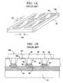
- FIG. 1 AA system constructed according to this approach is illustrated schematically in FIG. 1 A.
- the substrate or bottom chip 11has several chips 10 mounted thereon, with lateral spacing ⁇ x and ⁇ y.
- the bottom chip 11may be a DRAM chip while the four chips 10 are processor (“processor engine” or PE) chips.
- processorprocessor engine
- the different chipsare preferably in very close proximity and have very precise alignment with respect to each other.
- spacing ⁇ x and ⁇ y between chips 10is preferably about 50 ⁇ m or less.
- Chips 10may be placed on the substrate or bottom chip 11 with very high accuracy (within about 1 ⁇ m) by using a stud/via interconnection, shown schematically in FIG. 1 B.
- chip 10has metal studs 12 formed on the terminal surface of the chip, with a layer 16 of a low-melting-point alloy material deposited on the surface of the stud.
- Dielectric layer 17(often designed and fabricated as a multilayer structure of polyimide), on the surface of bottom chip 11 , has embedded therein high-density wiring 18 (generally several levels of Cu conductors, as shown schematically in FIG. 1 B), and has electrical joining pads 15 on the surface of layer 17 .
- a dielectric layer 14overlies the wiring layer 17 ; layer 14 may be formed of a polyimide material typically used in thin film packaging processing.
- Layer 14has vias 13 formed therein (e.g. by reactive-ion etching, by photolithography or by an excimer laser), so that a terminal metal joining pad 15 is at each via bottom.
- the viasmay be formed with a sloped wall angle as a guide for high-accuracy, self-aligned placement of the studs 12 in the vias 13 .
- a thin coating 19 of thermoplastic polymer adhesivemay be deposited on the top of the dielectric layer 14 , to ensure reliable bonding to the chip surface. Details of this stud/via alignment and joining process are provided in U.S.
- the wiring layerextends laterally outside the area of chips 10 .
- External connectionsare generally made at the perimeter 11 a of the top surface of bottom chip 11 .
- the overall size of the SOCtherefore limits the space available for wirebonding to make the external connections. It is desirable that the external connections instead be made through the backsides of the chips, so that the connections are not restricted by wirebonding space requirements.
- Formation of a connection pad (e.g. C4 pad) on the backside 10 b of a chipwould require that electrical connections be made vertically through the chip body, to the device side (surface 10 a ) of the chip.
- building vertical interconnections through a device chipwould facilitate vertical stacking of chips, effectively extending the SOC concept to three dimensions.
- the present inventionaddresses the above-described need by providing a process for vertical integration at chip level or wafer level, in which vertical connections are formed using a through-via in a chip.
- a methodfor fabricating a semiconductor structure.
- a featureis formed in the top surface of the substrate, and metal is deposited in the feature to make a conducting path.
- a linermay first be deposited in the feature to isolate the metal from the semiconductor material.
- a layeris then formed which overlies the top surface of the substrate; the layer includes an electrical conductor and a first conducting pad on a top surface of the layer, so that the first conducting pad is electrically connected to the feature.
- a plateis attached to this layer, and the substrate is then thinned at the bottom surface thereof to expose the bottom of the feature.
- a second conducting padis formed on the bottom surface of the substrate to make an electrical connection to the bottom of the feature, so that the first conducting pad and the second conducting pad are electrically connected through the feature.
- the substratemay comprise a chip having a device (e.g. DRAM) fabricated therein. Formation of a conducting path in a through-via in this chip therefore permits vertical integration with a second chip (e.g. a PE chip).
- a devicee.g. DRAM
- the platemay be a temporary handling plate to facilitate thinning of the substrate. If the plate is transparent to ablating radiation, it may be conveniently removed by ablating an interface between the layer and the plate.
- the plateis a semiconductor wafer which is not removed from the substrate; this wafer is attached to the substrate using a vertical stud/via interconnection.
- a second layeris formed on the above-described layer overlying the substrate, and a via is formed in the second layer exposing the first conducting pad.
- a studis formed on the semiconductor wafer and aligned to the via; the wafer is then contacted to the second layer so that the stud makes electrical connection with the first conducting pad.
- the substrate and platesemiconductor wafer
- the substrate and platemay each have devices fabricated therein (e.g. DRAM and PE devices respectively). This process thus provides vertical wafer-level integration of the devices.
- a semiconductor structurewhich includes a substrate; a first layer overlying the top surface of the substrate; conducting pads on top of the first layer and on the bottom surface of the substrate; a second layer on the first layer; and a plate contacting the first layer.
- the substratehas a via extending therethrough, with a first electrical conductor formed in the via.
- the first layerincludes a second electrical conductor connecting the first electrical conductor with the conducting pad on top of the layer.
- the conducting pad on the bottom surface of the substrateis electrically connected to the first electrical conductor, so that the first conducting pad and the second conducting pad are electrically connected.
- the second layerhas a via formed therein exposing the conducting pad on top of the first layer.
- the platehas a stud formed thereon, aligned to the via and making electrical contact with the conducting pad.
- the present inventionoffers a significant advantage in that the through-via is formed in the substrate without an expensive deep-via etching process. Via dimensions may be maintained with very high fidelity, which in turn permits a high density of through-vias. Furthermore, the use of vertical stud/via interconnections allows for highly accurate chip placement in the third dimension, similar to the highly accurate lateral chip placement described above.
- FIG. 1Ais a schematic illustration of system on a chip in which smaller chips are arranged on a larger chip and are intergrated and connected in close proximity.
- FIG. 1Billustrates a high accuracy, self-aligning stud/via interconnection scheme for the chips of FIG. 1 A.
- FIGS. 2A-2Fillustrate steps in a process for forming a vertical interconnection through the body of a chip, in accordance with an embodiment of the invention.
- FIGS. 3A-3Fillustrate steps in a process for obtaining chip-level integration of DRAM chips and processor (PE) chips using vertical interconnections, in accordance with an embodiment of the invention.
- FIG. 3Gillustrates an alternative chip-level integration using the vertical interconnections of FIG. 3 F.
- FIGS. 4A-4Eillustrate steps in a process for obtaining wafer-level integration of DRAM and PE wafers using vertical interconnections, in accordance with another embodiment of the invention.
- a semiconductor deviceis fabricated which includes vertical electrical connections through a chip. These vertical connections are formed by constructing metallized through-vias in the chip, without the need for expensive deep via etching.
- a DRAM chip(or silicon DRAM device wafer) is vertically connected to a plurality of PE chips (or a silicon PE device wafer). It will be appreciated that these types of chips are discussed for purposes of illustration only, and that the present invention may be practiced with a wide variety of chips and wafer types.
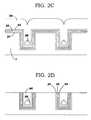
- a metallized through-via in a semiconductor substratesuch as a silicon wafer, may be formed by depositing metal in a trench and thinning the wafer to open the bottom of the trench, as detailed below.
- trenches 2are etched where the vertical connections are desired. As shown in FIG. 2A, the trenches do not extend through the wafer, but should extend into the bulk Si below the depth of the devices.
- An oxide layer 21is grown or deposited on the wafer and in the trenches.
- a trench liner 22typically of tungsten, is deposited on the oxide, preferably by chemical vapor deposition (CVD).
- a layer 23 of copperis then deposited on the liner.
- the deposition process for layer 23is ionized physical vapor deposition (IPVD), to ensure a thin, conformal coating of the interior of the trench.
- IPVDphysical vapor deposition
- a layer 24 of copperis formed on layer 23 (e.g. by electroplating) in the trench and on top of the wafer.
- Layer 24is built up on the sidewalls of the trench until it reaches a thickness such that the upper part of the trench is closed, as shown in FIG. 2 C.
- a conducting pathis established between the bottom of the trench and the top surface of the wafer, while a void 25 remains near the bottom of the trench.
- the void 25has an important function in relieving stresses caused by differences in the thermal coefficient of expansion (TCE) of the various materials in and around the feature.
- the waferis then planarized, preferably by chemical-mechanical polishing (CMP), to remove layers 21 - 24 from the top surface of the wafer.
- CMPchemical-mechanical polishing
- the resulting structureis shown in FIG. 2 D.
- the copper at the top of the trenchis then etched away (by reactive sputtering or some other convenient process) to a depth of about 5 ⁇ m, to yield the structure shown in FIG. 2E.
- a layer of tungstenis deposited on the wafer (preferably by CVD) and the wafer is again planarized using CMP, leaving a tungsten layer 26 at the top of each trench and an exposed surface 1 p of the silicon wafer (FIG. 2 F).
- the trench structure 20thus has copper metallization encased in tungsten.
- the waferis then ready to have devices formed therein near surface 1 p , and to be further processed to obtain either chip-level or wafer-level integration.
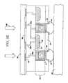
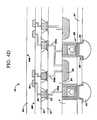
- Devices 30are fabricated in wafer 1 after the metallized trench structure 20 is completed. As shown in FIG. 3A, the devices are located in a region of wafer 1 adjacent to the top surface of the wafer. In this embodiment, devices 30 are DRAM devices. Dielectric layer 31 (typically polyimide) is then formed on top of the wafer; layer 31 has embedded therein high-density wiring 32 a - 32 c , and has on its top surface electrical joining pads 33 for making external connections (e.g. to PE chips on top of the DRAM chip). Examples of possible connections are shown schematically in FIG. 3 A.
- Dielectric layer 31typically polyimide
- layer 31has embedded therein high-density wiring 32 a - 32 c , and has on its top surface electrical joining pads 33 for making external connections (e.g. to PE chips on top of the DRAM chip). Examples of possible connections are shown schematically in FIG. 3 A.
- the electrical wiringmay connect a metallized via to a joining pad (conductor 32 a ); a device to a joining pad (conductor 32 b ); or a device to a via and/or a joining pad (conductor 32 c ).
- layer 31including the conductors, is shown as a single layer, it will be appreciated that for ease of manufacturing it is often designed and fabricated as a multilayer structure.
- Pads 33are typically formed as a multilayer structure including a Ti—W alloy, Ni, and Au, but may also include Cu, Co or other combinations of metals.
- Wafer 1is then thinned, by grinding, CMP, or some other convenient process, so that the interior of metallized via structure 20 is exposed at the bottom surface 1 b or backside of wafer 1 (FIG. 3 B).
- the thinned wafermay be difficult to handle or be incompatible with the equipment used in subsequent wafer processing. Accordingly, it may be desirable to attach a temporary handling plate to the wafer before the thinning process is performed, particularly if the final thickness of the wafer is less than 150 ⁇ m. In this embodiment, the wafer thickness is reduced to about 100 ⁇ m or less.
- a glass plate 35is attached to the top surface of layer 31 using a layer of adhesive 36 .
- Each via structure 20 at this pointis a through-via with tungsten layer 22 exposed on the bottom surface 1 b of the wafer.
- An insulating layer 37e.g. polyimide
- openings 38are formed therein, at the locations of the vias 20 .
- a metal layer(or combination of layers) is then deposited on layer 37 and patterned so that metal pads 39 are formed in and around the openings 38 .
- Pads 39typically have a structure similar to pads 33 ; that is, a multilayer structure including a Ti—W alloy, Ni, and Au. The resulting structure is shown in FIG. 3 C.
- Solder bumps 41are then formed on the back side of the wafer on pads 39 , using methods known in the art. For example, a solder paste may be applied to the wafer through a screen, and the deposited solder subjected to a reflow process.
- FIG. 3Dshows the wafer structure ready for dicing and joining to a carrier.
- the waferis diced into chips 44 while the glass handling plate 35 is kept intact, as shown in FIG. 3 E.
- the dicing processmay include dicing of plate 35 (thus requiring handling of individual chips in the joining process).
- the chipsare joined to a carrier 45 ; solder bumps 41 are typically connected to metal pads (not shown) at the top surface of the carrier.
- Carrier 45may be another chip, a ceramic substrate, a circuit board, etc.
- the temporary handling plate 35is removed from the chips. This may be conveniently done by a laser ablation process, as shown schematically in FIG. 3 E. Laser radiation 46 , incident on glass plate 35 , penetrates the plate and ablates the interface between the plate and the adhesive layer 36 . This results in delamination of the plate from layer 36 , so that plate 35 may be removed. The remaining adhesive is then cleaned away so that joining pads 33 are exposed.
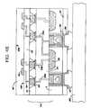
- FIG. 3Fvertical integration of DRAM chips 44 and PE chips 54 is accomplished by bonding the PE chips to the joining pads 33 of the DRAM chips.
- processing devices 50are fabricated in the wafer; otherwise the PE chips are prepared according to the same method as described above, with similar structures indicated by repeated reference numerals in FIG. 3 F.
- the joining pads 33 on the top surface of chips 54may be used to make external connections to the vertically integrated structure 55 , which includes a DRAM chip and a plurality of PE chips.
- the PE chipsmay be conventional chips 56 (having devices 51 in substrate 52 and wiring layer 31 ) without vertical through-via connections.
- the PE chips 56are joined to chips 44 (which have vertical through-via connections) to form integrated structure 57 .
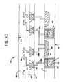
- a metallized through-viais formed in a wafer, and another wafer is joined thereto using stud/via interconnections.
- wafer 1has metallized trench structures 20 and devices 30 (e.g. DRAM devices) fabricated therein, with a dielectric layer 31 on top of the wafer containing electrical wiring and having pads 33 thereon (compare FIG. 3 A).
- the trench structuresare formed as described above with reference to FIGS. 2A-2F.
- the waferhas a dielectric layer 61 , typically of polyimide, overlying layer 31 .
- Layer 61has via openings 62 formed therein, to expose pads 33 .
- Another wafer 65having devices 60 (e.g. PE devices) near front surface 65 f , has a dielectric layer 63 formed thereon, with high-density wiring 64 for electrical connection to studs 66 .
- devices 60are connected to studs 66 , and the studs correspond with the vias 62 .
- Wafer 1 and wafer 65are then bonded together with studs 66 making electrical connection to pads 33 , as shown in FIG. 4 B. (The bonding may be facilitated by using a solder layer on the studs and/or an adhesive on the polyimide layer, as discussed above with reference to FIG. 1B.)
- the resulting wafer structure 70thus contains interconnected devices; it should be noted that wafers 1 and 65 may have different device types (such as DRAM and PE devices) and/or be of different materials (Si, SiGe, GaAs, etc.).
- Wafer 1is then thinned so that the trench structure 20 becomes a through-via, as in the previous embodiment (FIG. 4C; compare FIG. 3 B).
- wafer 65can function as a handling wafer while wafer 1 is thinned.
- wafer 65may also be processed to have through-vias extending to back surface 65 b ; in this case wafer 65 may require bonding to a temporary handling plate (not shown) which is subsequently removed, prior to bonding of wafer 65 to wafer 1 .
- An insulating layer 37(e.g. polyimide) is deposited on surface 1 b , and openings 38 are formed therein, as in the previous embodiment. Pads 39 are then formed to make connections to the through-vias, and solder bumps 41 are attached to the pads (FIG. 4 D).
- the wafer structure 70is then diced to produced combined chips 74 (e.g. combined DRAM/PE chips), which are then joined to carrier 45 , as shown in FIG. 4 E. Any temporary handling plate used for wafer 65 is removed at this point. It will be appreciated that if wafer 65 has through-vias to back surface 65 b , electrical connections may be made to the top surface of chip 74 . Accordingly, further vertical integration may be accomplished.
- combined chips 74e.g. combined DRAM/PE chips
Landscapes
- Engineering & Computer Science (AREA)
- Microelectronics & Electronic Packaging (AREA)
- Power Engineering (AREA)
- Computer Hardware Design (AREA)
- Physics & Mathematics (AREA)
- Condensed Matter Physics & Semiconductors (AREA)
- General Physics & Mathematics (AREA)
- Manufacturing & Machinery (AREA)
- Internal Circuitry In Semiconductor Integrated Circuit Devices (AREA)
Abstract
Description
Claims (16)
Priority Applications (10)
| Application Number | Priority Date | Filing Date | Title |
|---|---|---|---|
| US10/026,103US6599778B2 (en) | 2001-12-19 | 2001-12-19 | Chip and wafer integration process using vertical connections |
| AU2002352993AAU2002352993A1 (en) | 2001-12-19 | 2002-11-26 | Chip and wafer integration process using vertical connections |
| PCT/US2002/038355WO2003054956A1 (en) | 2001-12-19 | 2002-11-26 | Chip and wafer integration process using vertical connections |
| EP02789958AEP1470583A4 (en) | 2001-12-19 | 2002-11-26 | Chip and wafer integration process using vertical connections |
| JP2003555579AJP4366510B2 (en) | 2001-12-19 | 2002-11-26 | Chip and wafer integration method using vertical connection part |
| KR10-2004-7001450AKR100527232B1 (en) | 2001-12-19 | 2002-11-26 | Chip and wafer integration process using vertical connections |
| CNB028234030ACN1300840C (en) | 2001-12-19 | 2002-11-26 | Chip and wafer integration process using vertical connections |
| US10/465,506US6856025B2 (en) | 2001-12-19 | 2003-06-19 | Chip and wafer integration process using vertical connections |
| US11/033,926US7388277B2 (en) | 2001-12-19 | 2005-01-12 | Chip and wafer integration process using vertical connections |
| US12/114,145US7564118B2 (en) | 2001-12-19 | 2008-05-02 | Chip and wafer integration process using vertical connections |
Applications Claiming Priority (1)
| Application Number | Priority Date | Filing Date | Title |
|---|---|---|---|
| US10/026,103US6599778B2 (en) | 2001-12-19 | 2001-12-19 | Chip and wafer integration process using vertical connections |
Related Child Applications (1)
| Application Number | Title | Priority Date | Filing Date |
|---|---|---|---|
| US10/465,506DivisionUS6856025B2 (en) | 2001-12-19 | 2003-06-19 | Chip and wafer integration process using vertical connections |
Publications (2)
| Publication Number | Publication Date |
|---|---|
| US20030111733A1 US20030111733A1 (en) | 2003-06-19 |
| US6599778B2true US6599778B2 (en) | 2003-07-29 |
Family
ID=21829924
Family Applications (4)
| Application Number | Title | Priority Date | Filing Date |
|---|---|---|---|
| US10/026,103Expired - LifetimeUS6599778B2 (en) | 2001-12-19 | 2001-12-19 | Chip and wafer integration process using vertical connections |
| US10/465,506Expired - LifetimeUS6856025B2 (en) | 2001-12-19 | 2003-06-19 | Chip and wafer integration process using vertical connections |
| US11/033,926Expired - LifetimeUS7388277B2 (en) | 2001-12-19 | 2005-01-12 | Chip and wafer integration process using vertical connections |
| US12/114,145Expired - LifetimeUS7564118B2 (en) | 2001-12-19 | 2008-05-02 | Chip and wafer integration process using vertical connections |
Family Applications After (3)
| Application Number | Title | Priority Date | Filing Date |
|---|---|---|---|
| US10/465,506Expired - LifetimeUS6856025B2 (en) | 2001-12-19 | 2003-06-19 | Chip and wafer integration process using vertical connections |
| US11/033,926Expired - LifetimeUS7388277B2 (en) | 2001-12-19 | 2005-01-12 | Chip and wafer integration process using vertical connections |
| US12/114,145Expired - LifetimeUS7564118B2 (en) | 2001-12-19 | 2008-05-02 | Chip and wafer integration process using vertical connections |
Country Status (7)
| Country | Link |
|---|---|
| US (4) | US6599778B2 (en) |
| EP (1) | EP1470583A4 (en) |
| JP (1) | JP4366510B2 (en) |
| KR (1) | KR100527232B1 (en) |
| CN (1) | CN1300840C (en) |
| AU (1) | AU2002352993A1 (en) |
| WO (1) | WO2003054956A1 (en) |
Cited By (221)
| Publication number | Priority date | Publication date | Assignee | Title |
|---|---|---|---|---|
| US20030015788A1 (en)* | 2000-09-26 | 2003-01-23 | International Business Machines Corporation | Process for making fine pitch connections between devices and structure made by the process |
| US20030136993A1 (en)* | 2002-01-18 | 2003-07-24 | Infineon Technologies North America Corp. | System and method for back-side contact for trench semiconductor device characterization |
| US6864165B1 (en)* | 2003-09-15 | 2005-03-08 | International Business Machines Corporation | Method of fabricating integrated electronic chip with an interconnect device |
| US20060009029A1 (en)* | 2004-07-06 | 2006-01-12 | Agency For Science, Technology And Research | Wafer level through-hole plugging using mechanical forming technique |
| US20060035441A1 (en)* | 2003-09-30 | 2006-02-16 | Walter Rieger | Method for processing a thin semiconductor substrate |
| US7049695B1 (en) | 2005-01-14 | 2006-05-23 | International Business Machines Corporation | Method and device for heat dissipation in semiconductor modules |
| US20060121690A1 (en)* | 2002-12-20 | 2006-06-08 | Pogge H B | Three-dimensional device fabrication method |
| US20060252254A1 (en)* | 2005-05-06 | 2006-11-09 | Basol Bulent M | Filling deep and wide openings with defect-free conductor |
| US20060281243A1 (en)* | 2005-06-14 | 2006-12-14 | John Trezza | Through chip connection |
| US20060278995A1 (en)* | 2005-06-14 | 2006-12-14 | John Trezza | Chip spanning connection |
| US20070111385A1 (en)* | 2001-05-31 | 2007-05-17 | Magerlein John H | Method of manufacture of silicon based package and devices manufactured thereby |
| US20070161235A1 (en)* | 2005-06-14 | 2007-07-12 | John Trezza | Back-to-front via process |
| US20070238293A1 (en)* | 2006-03-29 | 2007-10-11 | Basol Bulent M | Filling deep features with conductors in semiconductor manufacturing |
| US20070293040A1 (en)* | 2006-03-29 | 2007-12-20 | Asm Nutool, Inc. | Filling deep features with conductors in semiconductor manufacturing |
| US20080090413A1 (en)* | 2006-10-17 | 2008-04-17 | John Trezza | Wafer via formation |
| US20080157787A1 (en)* | 2007-01-03 | 2008-07-03 | Cubic Wafer, Inc. | Sensitivity capacitive sensor |
| US20080197488A1 (en)* | 2007-02-15 | 2008-08-21 | John Trezza | Bowed wafer hybridization compensation |
| US20080197508A1 (en)* | 2007-02-16 | 2008-08-21 | John Trezza | Plated pillar package formation |
| US20080200022A1 (en)* | 2007-02-15 | 2008-08-21 | John Callahan | Post-seed deposition process |
| US20080197893A1 (en)* | 2007-02-15 | 2008-08-21 | Wyman Theodore J Ted | Variable off-chip drive |
| US20080242220A1 (en)* | 2007-03-29 | 2008-10-02 | Research In Motion Limited | Method, system and mobile device for prioritizing a discovered device list |
| US20080246145A1 (en)* | 2007-04-05 | 2008-10-09 | John Trezza | Mobile binding in an electronic connection |
| US20080245846A1 (en)* | 2007-04-05 | 2008-10-09 | John Trezza | Heat cycle-able connection |
| US20080261392A1 (en)* | 2007-04-23 | 2008-10-23 | John Trezza | Conductive via formation |
| US20090001598A1 (en)* | 2007-06-27 | 2009-01-01 | Wen-Chih Chiou | Formation of Through Via before Contact Processing |
| US20090065365A1 (en)* | 2007-09-11 | 2009-03-12 | Asm Nutool, Inc. | Method and apparatus for copper electroplating |
| US20090102021A1 (en)* | 2007-10-17 | 2009-04-23 | Chih-Hua Chen | Through-Silicon Vias and Methods for Forming the Same |
| US20090134500A1 (en)* | 2007-11-26 | 2009-05-28 | Chen-Cheng Kuo | Structures for Preventing Cross-talk Between Through-Silicon Vias and Integrated Circuits |
| US20090163790A1 (en)* | 2004-07-13 | 2009-06-25 | Dexcom, Inc. | Transcutaneous analyte sensor |
| US7560813B2 (en) | 2005-06-14 | 2009-07-14 | John Trezza | Chip-based thermo-stack |
| US20090186430A1 (en)* | 2007-05-24 | 2009-07-23 | Chih-Hua Chen | Test Patterns for Detecting Misalignment of Through-Wafer Vias |
| US20090193584A1 (en)* | 2008-02-05 | 2009-08-06 | Standard Textile Co., Inc. | Woven contoured bed sheet with elastomeric yarns |
| US20090267219A1 (en)* | 2007-04-23 | 2009-10-29 | John Trezza | Ultra-thin chip packaging |
| US20090283871A1 (en)* | 2008-05-14 | 2009-11-19 | Hung-Pin Chang | System, Structure, and Method of Manufacturing a Semiconductor Substrate Stack |
| US20090294983A1 (en)* | 2008-06-03 | 2009-12-03 | Micron Technology, Inc. | Hybrid conductive vias including small dimension active surface ends and larger dimension back side ends, semiconductor devices including the same, and associated methods |
| US20090321888A1 (en)* | 2007-12-06 | 2009-12-31 | Taiwan Semiconductor Manufacturing Company, Ltd. | Alignment for backside illumination sensor |
| US20100006972A1 (en)* | 2008-07-14 | 2010-01-14 | International Business Machines Corporation | Wafer scale membrane for three-dimensional integrated circuit device fabrication |
| US7659202B2 (en) | 2005-06-14 | 2010-02-09 | John Trezza | Triaxial through-chip connection |
| US20100038674A1 (en)* | 2008-08-18 | 2010-02-18 | Ding-Yuan Chen | Light-Emitting Diode With Current-Spreading Region |
| US20100062693A1 (en)* | 2008-09-05 | 2010-03-11 | Taiwan Semiconductor Manufacturing Co., Ltd. | Two step method and apparatus for polishing metal and other films in semiconductor manufacturing |
| US7687397B2 (en) | 2006-06-06 | 2010-03-30 | John Trezza | Front-end processed wafer having through-chip connections |
| US7687400B2 (en) | 2005-06-14 | 2010-03-30 | John Trezza | Side stacking apparatus and method |
| US20100078770A1 (en)* | 2008-09-26 | 2010-04-01 | International Business Machines Corporation | Lock and Key Through-Via Method for Wafer Level 3 D Integration and Structures Produced |
| US20100084747A1 (en)* | 2008-10-03 | 2010-04-08 | Chih-Hua Chen | Zigzag Pattern for TSV Copper Adhesion |
| US20100090304A1 (en)* | 2008-09-08 | 2010-04-15 | Taiwan Semiconductor Manufacturing Company, Ltd. | Bonding process for cmos image sensor |
| US20100117226A1 (en)* | 2008-11-07 | 2010-05-13 | Ku-Feng Yang | Structure and method for stacked wafer fabrication |
| US20100117201A1 (en)* | 2008-11-13 | 2010-05-13 | Kai-Ming Ching | Cooling Channels in 3DIC Stacks |
| US20100133695A1 (en)* | 2003-01-12 | 2010-06-03 | Sang-Yun Lee | Electronic circuit with embedded memory |
| US20100144094A1 (en)* | 2008-12-05 | 2010-06-10 | Ming-Fa Chen | Method of Forming Stacked Dies |
| US20100140805A1 (en)* | 2008-12-10 | 2010-06-10 | Hung-Pin Chang | Bump Structure for Stacked Dies |
| US20100148371A1 (en)* | 2008-12-12 | 2010-06-17 | Qualcomm Incorporated | Via First Plus Via Last Technique for IC Interconnects |
| US20100164109A1 (en)* | 2008-12-29 | 2010-07-01 | Wen-Chih Chiou | Backside Metal Treatment of Semiconductor Chips |
| US20100167467A1 (en)* | 2008-09-26 | 2010-07-01 | Panasonic Corporation | Method for fabricating semiconductor device |
| US20100171197A1 (en)* | 2009-01-05 | 2010-07-08 | Hung-Pin Chang | Isolation Structure for Stacked Dies |
| US20100171203A1 (en)* | 2009-01-07 | 2010-07-08 | Taiwan Semiconductor Manufacturing Company | Robust TSV structure |
| US20100176494A1 (en)* | 2009-01-13 | 2010-07-15 | Ming-Fa Chen | Through-Silicon Via With Low-K Dielectric Liner |
| US20100187670A1 (en)* | 2009-01-26 | 2010-07-29 | Chuan-Yi Lin | On-Chip Heat Spreader |
| US20100187671A1 (en)* | 2009-01-26 | 2010-07-29 | Chuan-Yi Lin | Forming Seal Ring in an Integrated Circuit Die |
| US20100193954A1 (en)* | 2009-02-04 | 2010-08-05 | Max Liu | Barrier Structures and Methods for Through Substrate Vias |
| US20100194014A1 (en)* | 2009-02-02 | 2010-08-05 | Jao Sheng Huang | Semiconductor Wafer Carrier |
| US20100200992A1 (en)* | 2008-09-26 | 2010-08-12 | International Business Machines Corporation | Lock and Key Through-Via Method for Wafer Level 3D Integration and Structures Produced |
| US20100200989A1 (en)* | 2009-02-12 | 2010-08-12 | Asm International, N.V. | Liner materials and related processes for 3-d integration |
| US7781886B2 (en) | 2005-06-14 | 2010-08-24 | John Trezza | Electronic chip contact structure |
| US20100213560A1 (en)* | 2009-02-24 | 2010-08-26 | Taiwan Semiconductor Manufacturing Company, Ltd. | Pad design for backside illuminated image sensor |
| US7786592B2 (en) | 2005-06-14 | 2010-08-31 | John Trezza | Chip capacitive coupling |
| US20100220226A1 (en)* | 2009-02-24 | 2010-09-02 | Taiwan Semiconductor Manufacturing Company, Ltd. | Front side implanted guard ring structure for backside illuminated image sensor |
| US20100224966A1 (en)* | 2009-03-03 | 2010-09-09 | Taiwan Semiconductor Manufacturing Company, Ltd. | Stress Barrier Structures for Semiconductor Chips |
| US20100225002A1 (en)* | 2009-03-06 | 2010-09-09 | Taiwan Semiconductor Manufacturing Company, Ltd. | Three-Dimensional System-in-Package Architecture |
| US20100237502A1 (en)* | 2009-03-23 | 2010-09-23 | Taiwan Semiconductor Manufacturing Company, Ltd. | Barrier for Through-Silicon Via |
| US20100244247A1 (en)* | 2009-03-27 | 2010-09-30 | Taiwan Semiconductor Manufacturing Company, Ltd. | Via structure and via etching process of forming the same |
| US20100244284A1 (en)* | 2009-03-27 | 2010-09-30 | Taiwan Semiconductor Manufacturing Company, Ltd. | Method for ultra thin wafer handling and processing |
| US20100252934A1 (en)* | 2009-04-07 | 2010-10-07 | Taiwan Semiconductor Manufacturing Company, Ltd. | Three-Dimensional Semiconductor Architecture |
| US20100267217A1 (en)* | 2009-04-20 | 2010-10-21 | Taiwan Semiconductor Manufacturing Company, Ltd. | Backside Process for a Substrate |
| US20100276787A1 (en)* | 2009-04-30 | 2010-11-04 | Taiwan Semiconductor Manufacturing Company, Ltd. | Wafer Backside Structures Having Copper Pillars |
| US7829975B2 (en)* | 1996-12-02 | 2010-11-09 | Kabushiki Kaisha Toshiba | Multichip semiconductor device, chip therefor and method of formation thereof |
| US7838997B2 (en) | 2005-06-14 | 2010-11-23 | John Trezza | Remote chip attachment |
| US7851348B2 (en) | 2005-06-14 | 2010-12-14 | Abhay Misra | Routingless chip architecture |
| US20100314758A1 (en)* | 2009-06-12 | 2010-12-16 | Taiwan Semiconductor Manufacturing Company, Ltd. | Through-silicon via structure and a process for forming the same |
| US20100330788A1 (en)* | 2009-06-30 | 2010-12-30 | Taiwan Semiconductor Manufacturing Company, Ltd. | Thin wafer handling structure and method |
| US20100330798A1 (en)* | 2009-06-26 | 2010-12-30 | Taiwan Semiconductor Manufacturing Company, Ltd. | Formation of TSV Backside Interconnects by Modifying Carrier Wafers |
| US20110006428A1 (en)* | 2009-07-08 | 2011-01-13 | Ching-Yu Lo | Liner Formation in 3DIC Structures |
| US20110027944A1 (en)* | 2009-07-30 | 2011-02-03 | Taiwan Semiconductor Maufacturing Company, Ltd. | Method of forming electrical connections |
| US20110035937A1 (en)* | 2009-08-14 | 2011-02-17 | Taiwan Semiconductor Manufacturing Company, Ltd. | Semiconductor Wafer Carrier and Method of Manufacturing |
| US20110049706A1 (en)* | 2009-09-03 | 2011-03-03 | Taiwan Semiconductor Manufacturing Company, Ltd. | Front Side Copper Post Joint Structure for Temporary Bond in TSV Application |
| US20110065238A1 (en)* | 2009-09-14 | 2011-03-17 | Taiwan Semiconductor Manufacturing Company, Ltd. | Protection layer for adhesive material at wafer edge |
| US20110068466A1 (en)* | 2009-09-22 | 2011-03-24 | Taiwan Semiconductor Manufacturing Company, Ltd. | Wafer Backside Interconnect Structure Connected to TSVs |
| US20110078127A1 (en)* | 2009-09-27 | 2011-03-31 | Alibaba Group Holding Limited | Searching for information based on generic attributes of the query |
| US20110081749A1 (en)* | 2009-10-01 | 2011-04-07 | Taiwan Semiconductor Manufacturing Company, Ltd. | Surface modification for handling wafer thinning process |
| US20110084365A1 (en)* | 2009-10-09 | 2011-04-14 | Taiwan Semiconductor Manufacturing Company, Ltd. | Through Silicon Via (TSV) Wire Bond Architecture |
| US20110101527A1 (en)* | 2009-11-05 | 2011-05-05 | Taiwan Semiconductor Manufacturing Company, Ltd. | Mechanisms for forming copper pillar bumps |
| US20110108986A1 (en)* | 2009-11-09 | 2011-05-12 | Taiwan Semiconductor Manufacturing Company, Ltd. | Through-silicon via structure and a process for forming the same |
| US20110108940A1 (en)* | 2009-11-06 | 2011-05-12 | Taiwan Semiconductor Manufacturing Company, Ltd. | Method of fabricating backside-illuminated image sensor |
| US20110111560A1 (en)* | 2008-09-26 | 2011-05-12 | International Business Machines Corporation | Lock and Key Through-Via Method for Wafer Level 3D Integration and Structures Produced Thereby |
| US20110133335A1 (en)* | 2008-12-31 | 2011-06-09 | Taiwan Semiconductor Manufacturing Company, Ltd. | Through-Silicon Via With Air Gap |
| US20110169168A1 (en)* | 2009-02-24 | 2011-07-14 | Taiwan Semiconductor Manufacturing Company, Ltd. | Through-silicon via formed with a post passivation interconnect structure |
| US20110170266A1 (en)* | 2010-01-08 | 2011-07-14 | Ibm Corporation | 4d device process and structure |
| US20110193219A1 (en)* | 2010-02-09 | 2011-08-11 | Taiwan Seimconductor Manufacturing Company, Ltd. | Semiconductor device and semiconductor assembly with lead-free solder |
| US20110193221A1 (en)* | 2010-02-05 | 2011-08-11 | Taiwan Semiconductor Manufacturing Company, Ltd. | 3DIC Architecture with Interposer for Bonding Dies |
| US20110193199A1 (en)* | 2010-02-09 | 2011-08-11 | International Business Machines Corporation | Electromigration immune through-substrate vias |
| US20110198747A1 (en)* | 2010-02-16 | 2011-08-18 | Taiwan Semicondcutor Manufactoring Company, Ltd. | Conductive pillar structure for semiconductor substrate and method of manufacture |
| US20110198721A1 (en)* | 2010-02-12 | 2011-08-18 | Taiwan Semiconductor Manufacturing Company, Ltd. | Method for thinning a wafer |
| US20110198638A1 (en)* | 2010-02-16 | 2011-08-18 | Taiwan Semiconductor Manufacturing Company, Ltd. | Light-emitting diode (led) package systems |
| US20110217841A1 (en)* | 2009-10-22 | 2011-09-08 | Taiwan Semiconductor Manufacturing Company, Ltd. | Method of forming through silicon via with dummy structure |
| US20110233761A1 (en)* | 2009-07-30 | 2011-09-29 | Taiwan Semiconductor Manufacturing Company, Ltd. | Cu pillar bump with non-metal sidewall protection structure |
| US8174124B2 (en) | 2010-04-08 | 2012-05-08 | Taiwan Semiconductor Manufacturing Co., Ltd. | Dummy pattern in wafer backside routing |
| US8222139B2 (en) | 2010-03-30 | 2012-07-17 | Taiwan Semiconductor Manufacturing Company, Ltd. | Chemical mechanical polishing (CMP) processing of through-silicon via (TSV) and contact plug simultaneously |
| US8236584B1 (en) | 2011-02-11 | 2012-08-07 | Tsmc Solid State Lighting Ltd. | Method of forming a light emitting diode emitter substrate with highly reflective metal bonding |
| US8247906B2 (en) | 2009-07-06 | 2012-08-21 | Taiwan Semiconductor Manufacturing Company, Ltd. | Supplying power to integrated circuits using a grid matrix formed of through-silicon vias |
| US8319336B2 (en) | 2010-07-08 | 2012-11-27 | Taiwan Semiconductor Manufacturing Company, Ltd. | Reduction of etch microloading for through silicon vias |
| US8324738B2 (en) | 2009-09-01 | 2012-12-04 | Taiwan Semiconductor Manufacturing Company, Ltd. | Self-aligned protection layer for copper post structure |
| US8330262B2 (en) | 2010-02-02 | 2012-12-11 | International Business Machines Corporation | Processes for enhanced 3D integration and structures generated using the same |
| US8338939B2 (en) | 2010-07-12 | 2012-12-25 | Taiwan Semiconductor Manufacturing Company, Ltd. | TSV formation processes using TSV-last approach |
| US8362591B2 (en) | 2010-06-08 | 2013-01-29 | Taiwan Semiconductor Manufacturing Co., Ltd. | Integrated circuits and methods of forming the same |
| US8411459B2 (en) | 2010-06-10 | 2013-04-02 | Taiwan Semiconductor Manufacturing Company, Ltd | Interposer-on-glass package structures |
| US8441124B2 (en) | 2010-04-29 | 2013-05-14 | Taiwan Semiconductor Manufacturing Company, Ltd. | Cu pillar bump with non-metal sidewall protection structure |
| US8445296B2 (en) | 2011-07-22 | 2013-05-21 | Taiwan Semiconductor Manufacturing Company, Ltd. | Apparatus and methods for end point determination in reactive ion etching |
| US8455995B2 (en) | 2010-04-16 | 2013-06-04 | Taiwan Semiconductor Manufacturing Company, Ltd. | TSVs with different sizes in interposers for bonding dies |
| US8456008B2 (en) | 2007-12-21 | 2013-06-04 | Taiwan Semiconductor Manufacturing Company, Ltd. | Structure and process for the formation of TSVs |
| US8456015B2 (en) | 2005-06-14 | 2013-06-04 | Cufer Asset Ltd. L.L.C. | Triaxial through-chip connection |
| US8461045B2 (en) | 2008-10-09 | 2013-06-11 | Taiwan Semiconductor Manufacturing Company, Ltd. | Bond pad connection to redistribution lines having tapered profiles |
| US8466059B2 (en) | 2010-03-30 | 2013-06-18 | Taiwan Semiconductor Manufacturing Company, Ltd. | Multi-layer interconnect structure for stacked dies |
| US8471358B2 (en) | 2010-06-01 | 2013-06-25 | Taiwan Semiconductor Manufacturing Company, Ltd. | 3D inductor and transformer |
| US8476735B2 (en) | 2007-05-29 | 2013-07-02 | Taiwan Semiconductor Manufacturing Company, Ltd. | Programmable semiconductor interposer for electronic package and method of forming |
| US8487410B2 (en) | 2011-04-13 | 2013-07-16 | Taiwan Semiconductor Manufacturing Company, Ltd. | Through-silicon vias for semicondcutor substrate and method of manufacture |
| US8502338B2 (en) | 2010-09-09 | 2013-08-06 | Taiwan Semiconductor Manufacturing Company, Ltd. | Through-substrate via waveguides |
| US8500182B2 (en) | 2010-06-17 | 2013-08-06 | Taiwan Semiconductor Manufacturing Company, Ltd. | Vacuum wafer carriers for strengthening thin wafers |
| US8501587B2 (en) | 2009-01-13 | 2013-08-06 | Taiwan Semiconductor Manufacturing Company, Ltd. | Stacked integrated chips and methods of fabrication thereof |
| US8507358B2 (en) | 2010-08-27 | 2013-08-13 | Taiwan Semiconductor Manufacturing Company, Ltd. | Composite wafer semiconductor |
| US8507940B2 (en) | 2010-04-05 | 2013-08-13 | Taiwan Semiconductor Manufacturing Company, Ltd. | Heat dissipation by through silicon plugs |
| US8519538B2 (en) | 2010-04-28 | 2013-08-27 | Taiwan Semiconductor Manufacturing Company, Ltd. | Laser etch via formation |
| US8519409B2 (en) | 2010-11-15 | 2013-08-27 | Taiwan Semiconductor Manufacturing Company, Ltd. | Light emitting diode components integrated with thermoelectric devices |
| US8525343B2 (en) | 2010-09-28 | 2013-09-03 | Taiwan Semiconductor Manufacturing Company, Ltd. | Device with through-silicon via (TSV) and method of forming the same |
| US8525278B2 (en) | 2011-08-19 | 2013-09-03 | Taiwan Semiconductor Manufacturing Company, Ltd. | MEMS device having chip scale packaging |
| US8531035B2 (en) | 2011-07-01 | 2013-09-10 | Taiwan Semiconductor Manufacturing Company, Ltd. | Interconnect barrier structure and method |
| US8546235B2 (en) | 2011-05-05 | 2013-10-01 | Taiwan Semiconductor Manufacturing Company, Ltd. | Integrated circuits including metal-insulator-metal capacitors and methods of forming the same |
| US8546254B2 (en) | 2010-08-19 | 2013-10-01 | Taiwan Semiconductor Manufacturing Company, Ltd. | Mechanisms for forming copper pillar bumps using patterned anodes |
| US8546886B2 (en) | 2011-08-24 | 2013-10-01 | Taiwan Semiconductor Manufacturing Company, Ltd. | Controlling the device performance by forming a stressed backside dielectric layer |
| US8546953B2 (en) | 2011-12-13 | 2013-10-01 | Taiwan Semiconductor Manufacturing Co., Ltd. | Through silicon via (TSV) isolation structures for noise reduction in 3D integrated circuit |
| US8552485B2 (en) | 2011-06-15 | 2013-10-08 | Taiwan Semiconductor Manufacturing Company, Ltd. | Semiconductor structure having metal-insulator-metal capacitor structure |
| US8567837B2 (en) | 2010-11-24 | 2013-10-29 | Taiwan Semiconductor Manufacturing Company, Ltd. | Reconfigurable guide pin design for centering wafers having different sizes |
| US8580647B2 (en) | 2011-12-19 | 2013-11-12 | Taiwan Semiconductor Manufacturing Company, Ltd. | Inductors with through VIAS |
| US8580682B2 (en) | 2010-09-30 | 2013-11-12 | Taiwan Semiconductor Manufacturing Company, Ltd. | Cost-effective TSV formation |
| US8587127B2 (en) | 2011-06-15 | 2013-11-19 | Taiwan Semiconductor Manufacturing Company, Ltd. | Semiconductor structures and methods of forming the same |
| US8604619B2 (en) | 2011-08-31 | 2013-12-10 | Taiwan Semiconductor Manufacturing Company, Ltd. | Through silicon via keep out zone formation along different crystal orientations |
| US8604491B2 (en) | 2011-07-21 | 2013-12-10 | Tsmc Solid State Lighting Ltd. | Wafer level photonic device die structure and method of making the same |
| US8610247B2 (en) | 2011-12-30 | 2013-12-17 | Taiwan Semiconductor Manufacturing Company, Ltd. | Structure and method for a transformer with magnetic features |
| US8618631B2 (en) | 2012-02-14 | 2013-12-31 | Taiwan Semiconductor Manufacturing Co., Ltd. | On-chip ferrite bead inductor |
| US8629563B2 (en) | 2007-07-16 | 2014-01-14 | Taiwan Semiconductor Manufacturing Company, Ltd. | Method for packaging semiconductor dies having through-silicon vias |
| US8629042B2 (en) | 2008-12-08 | 2014-01-14 | Taiwan Semiconductor Manufacturing Company, Ltd. | Method for stacking semiconductor dies |
| US8659126B2 (en) | 2011-12-07 | 2014-02-25 | Taiwan Semiconductor Manufacturing Company, Ltd. | Integrated circuit ground shielding structure |
| US8674510B2 (en) | 2010-07-29 | 2014-03-18 | Taiwan Semiconductor Manufacturing Company, Ltd. | Three-dimensional integrated circuit structure having improved power and thermal management |
| US8674883B2 (en) | 2011-05-24 | 2014-03-18 | Taiwan Semiconductor Manufacturing Company, Ltd. | Antenna using through-silicon via |
| US8693163B2 (en) | 2010-09-01 | 2014-04-08 | Taiwan Semiconductor Manufacturing Company, Ltd. | Cylindrical embedded capacitors |
| US8703609B2 (en) | 2007-08-24 | 2014-04-22 | Taiwan Semiconductor Manufacturing Company, Ltd. | Through-substrate via for semiconductor device |
| US8716131B2 (en) | 2008-08-05 | 2014-05-06 | Taiwan Semiconductor Manufacturing Company, Ltd. | Through silicon via layout |
| US8716128B2 (en) | 2011-04-14 | 2014-05-06 | Tsmc Solid State Lighting Ltd. | Methods of forming through silicon via openings |
| US8722540B2 (en) | 2010-07-22 | 2014-05-13 | Taiwan Semiconductor Manufacturing Company, Ltd. | Controlling defects in thin wafer handling |
| US8748284B2 (en) | 2011-08-12 | 2014-06-10 | Taiwan Semiconductor Manufacturing Company, Ltd. | Method of manufacturing decoupling MIM capacitor designs for interposers |
| US8766409B2 (en) | 2011-06-24 | 2014-07-01 | Taiwan Semiconductor Manufacturing Co., Ltd. | Method and structure for through-silicon via (TSV) with diffused isolation well |
| US8773866B2 (en) | 2010-12-10 | 2014-07-08 | Taiwan Semiconductor Manufacturing Company, Ltd. | Radio-frequency packaging with reduced RF loss |
| TWI447881B (en)* | 2009-03-09 | 2014-08-01 | United Microelectronics Corp | Through-silicon via structure and method for making the same |
| US8803322B2 (en) | 2011-10-13 | 2014-08-12 | Taiwan Semiconductor Manufacturing Company, Ltd. | Through substrate via structures and methods of forming the same |
| US8803316B2 (en) | 2011-12-06 | 2014-08-12 | Taiwan Semiconductor Manufacturing Company, Ltd. | TSV structures and methods for forming the same |
| US8809073B2 (en) | 2011-08-03 | 2014-08-19 | Taiwan Semiconductor Manufacturing Company, Ltd. | Apparatus and methods for de-embedding through substrate vias |
| US8836116B2 (en) | 2010-10-21 | 2014-09-16 | Taiwan Semiconductor Manufacturing Company, Ltd. | Wafer level packaging of micro-electro-mechanical systems (MEMS) and complementary metal-oxide-semiconductor (CMOS) substrates |
| US8846499B2 (en) | 2010-08-17 | 2014-09-30 | Taiwan Semiconductor Manufacturing Company, Ltd. | Composite carrier structure |
| US8860114B2 (en) | 2012-03-02 | 2014-10-14 | Taiwan Semiconductor Manufacturing Company, Ltd. | Structure and method for a fishbone differential capacitor |
| US8866301B2 (en) | 2010-05-18 | 2014-10-21 | Taiwan Semiconductor Manufacturing Company, Ltd. | Package systems having interposers with interconnection structures |
| US8872345B2 (en) | 2011-07-07 | 2014-10-28 | Taiwan Semiconductor Manufacturing Company, Ltd. | Forming grounded through-silicon vias in a semiconductor substrate |
| US8890293B2 (en) | 2011-12-16 | 2014-11-18 | Taiwan Semiconductor Manufacturing Company, Ltd. | Guard ring for through vias |
| US8896089B2 (en) | 2011-11-09 | 2014-11-25 | Taiwan Semiconductor Manufacturing Company, Ltd. | Interposers for semiconductor devices and methods of manufacture thereof |
| US8896136B2 (en) | 2010-06-30 | 2014-11-25 | Taiwan Semiconductor Manufacturing Company, Ltd. | Alignment mark and method of formation |
| US8900994B2 (en) | 2011-06-09 | 2014-12-02 | Taiwan Semiconductor Manufacturing Company, Ltd. | Method for producing a protective structure |
| US8928159B2 (en) | 2010-09-02 | 2015-01-06 | Taiwan Semiconductor Manufacturing & Company, Ltd. | Alignment marks in substrate having through-substrate via (TSV) |
| US8928127B2 (en) | 2010-09-24 | 2015-01-06 | Taiwan Semiconductor Manufacturing Company, Ltd. | Noise decoupling structure with through-substrate vias |
| US8999179B2 (en) | 2010-07-13 | 2015-04-07 | Taiwan Semiconductor Manufacturing Company, Ltd. | Conductive vias in a substrate |
| US9018758B2 (en) | 2010-06-02 | 2015-04-28 | Taiwan Semiconductor Manufacturing Company, Ltd. | Cu pillar bump with non-metal sidewall spacer and metal top cap |
| US9041152B2 (en) | 2013-03-14 | 2015-05-26 | Taiwan Semiconductor Manufacturing Company, Ltd. | Inductor with magnetic material |
| US9048233B2 (en) | 2010-05-26 | 2015-06-02 | Taiwan Semiconductor Manufacturing Company, Ltd. | Package systems having interposers |
| US9059026B2 (en) | 2010-06-01 | 2015-06-16 | Taiwan Semiconductor Manufacturing Company, Ltd. | 3-D inductor and transformer |
| US9059262B2 (en) | 2011-02-24 | 2015-06-16 | Taiwan Semiconductor Manufacturing Company, Ltd. | Integrated circuits including conductive structures through a substrate and methods of making the same |
| US9087838B2 (en) | 2011-10-25 | 2015-07-21 | Taiwan Semiconductor Manufacturing Company, Ltd. | Structure and method for a high-K transformer with capacitive coupling |
| US9139420B2 (en) | 2012-04-18 | 2015-09-22 | Taiwan Semiconductor Manufacturing Company, Ltd. | MEMS device structure and methods of forming same |
| US9153462B2 (en) | 2010-12-09 | 2015-10-06 | Taiwan Semiconductor Manufacturing Company, Ltd. | Spin chuck for thin wafer cleaning |
| US9159907B2 (en) | 2011-08-04 | 2015-10-13 | Taiwan Semiconductor Manufacturing Company, Ltd. | Hybrid film for protecting MTJ stacks of MRAM |
| US9190325B2 (en) | 2010-09-30 | 2015-11-17 | Taiwan Semiconductor Manufacturing Company, Ltd. | TSV formation |
| US9293521B2 (en) | 2012-03-02 | 2016-03-22 | Taiwan Semiconductor Manufacturing Co., Ltd. | Concentric capacitor structure |
| US9293366B2 (en) | 2010-04-28 | 2016-03-22 | Taiwan Semiconductor Manufacturing Company, Ltd. | Through-substrate vias with improved connections |
| US9299660B2 (en) | 2011-11-14 | 2016-03-29 | Intel Corporation | Controlled solder-on-die integrations on packages and methods of assembling same |
| US9299594B2 (en) | 2010-07-27 | 2016-03-29 | Taiwan Semiconductor Manufacturing Company, Ltd. | Substrate bonding system and method of modifying the same |
| US9305769B2 (en) | 2009-06-30 | 2016-04-05 | Taiwan Semiconductor Manufacturing Company, Ltd. | Thin wafer handling method |
| US9312432B2 (en) | 2012-03-13 | 2016-04-12 | Tsmc Solid State Lighting Ltd. | Growing an improved P-GaN layer of an LED through pressure ramping |
| US9390949B2 (en) | 2011-11-29 | 2016-07-12 | Taiwan Semiconductor Manufacturing Company, Ltd. | Wafer debonding and cleaning apparatus and method of use |
| US20160233161A1 (en)* | 2012-09-20 | 2016-08-11 | Taiwan Semiconductor Manufacturing Company, Ltd. | Passive Devices in Package-on-Package Structures and Methods for Forming the Same |
| US9484211B2 (en) | 2013-01-24 | 2016-11-01 | Taiwan Semiconductor Manufacturing Company, Ltd. | Etchant and etching process |
| US9490133B2 (en) | 2013-01-24 | 2016-11-08 | Taiwan Semiconductor Manufacturing Company, Ltd. | Etching apparatus |
| US9524945B2 (en) | 2010-05-18 | 2016-12-20 | Taiwan Semiconductor Manufacturing Company, Ltd. | Cu pillar bump with L-shaped non-metal sidewall protection structure |
| US9583365B2 (en) | 2012-05-25 | 2017-02-28 | Taiwan Semiconductor Manufacturing Company, Ltd. | Method of forming interconnects for three dimensional integrated circuit |
| US9618712B2 (en) | 2012-02-23 | 2017-04-11 | Taiwan Semiconductor Manufacturing Company, Ltd. | Optical bench on substrate and method of making the same |
| US9675443B2 (en) | 2009-09-10 | 2017-06-13 | Johnson & Johnson Vision Care, Inc. | Energized ophthalmic lens including stacked integrated components |
| US9698129B2 (en) | 2011-03-18 | 2017-07-04 | Johnson & Johnson Vision Care, Inc. | Stacked integrated component devices with energization |
| US9703120B2 (en) | 2011-02-28 | 2017-07-11 | Johnson & Johnson Vision Care, Inc. | Methods and apparatus for an ophthalmic lens with functional insert layers |
| US9804418B2 (en) | 2011-03-21 | 2017-10-31 | Johnson & Johnson Vision Care, Inc. | Methods and apparatus for functional insert with power layer |
| US9889615B2 (en) | 2011-03-18 | 2018-02-13 | Johnson & Johnson Vision Care, Inc. | Stacked integrated component media insert for an ophthalmic device |
| US9994741B2 (en) | 2015-12-13 | 2018-06-12 | International Business Machines Corporation | Enhanced adhesive materials and processes for 3D applications |
| US10180547B2 (en) | 2012-02-23 | 2019-01-15 | Taiwan Semiconductor Manufacturing Company, Ltd. | Optical bench on substrate |
| US10345620B2 (en) | 2016-02-18 | 2019-07-09 | Johnson & Johnson Vision Care, Inc. | Methods and apparatus to form biocompatible energization elements incorporating fuel cells for biomedical devices |
| US10361404B2 (en) | 2014-08-21 | 2019-07-23 | Johnson & Johnson Vision Care, Inc. | Anodes for use in biocompatible energization elements |
| US10361405B2 (en) | 2014-08-21 | 2019-07-23 | Johnson & Johnson Vision Care, Inc. | Biomedical energization elements with polymer electrolytes |
| US10367233B2 (en) | 2014-08-21 | 2019-07-30 | Johnson & Johnson Vision Care, Inc. | Biomedical energization elements with polymer electrolytes and cavity structures |
| US10374216B2 (en) | 2014-08-21 | 2019-08-06 | Johnson & Johnson Vision Care, Inc. | Pellet form cathode for use in a biocompatible battery |
| US10381254B2 (en) | 2011-11-29 | 2019-08-13 | Taiwan Semiconductor Manufacturing Co., Ltd. | Wafer debonding and cleaning apparatus and method |
| US10381687B2 (en) | 2014-08-21 | 2019-08-13 | Johnson & Johnson Vision Care, Inc. | Methods of forming biocompatible rechargable energization elements for biomedical devices |
| US10386656B2 (en) | 2014-08-21 | 2019-08-20 | Johnson & Johnson Vision Care, Inc. | Methods and apparatus to form separators for biocompatible energization elements for biomedical devices |
| US10451897B2 (en) | 2011-03-18 | 2019-10-22 | Johnson & Johnson Vision Care, Inc. | Components with multiple energization elements for biomedical devices |
| US10558062B2 (en) | 2014-08-21 | 2020-02-11 | Johnson & Johnson Vision Care, Inc. | Methods and apparatus to form biocompatible energization primary elements for biomedical device |
| US10598958B2 (en) | 2014-08-21 | 2020-03-24 | Johnson & Johnson Vision Care, Inc. | Device and methods for sealing and encapsulation for biocompatible energization elements |
| US10627651B2 (en) | 2014-08-21 | 2020-04-21 | Johnson & Johnson Vision Care, Inc. | Methods and apparatus to form biocompatible energization primary elements for biomedical devices with electroless sealing layers |
| US10775644B2 (en) | 2012-01-26 | 2020-09-15 | Johnson & Johnson Vision Care, Inc. | Ophthalmic lens assembly having an integrated antenna structure |
| US11257741B2 (en) | 2019-05-28 | 2022-02-22 | Samsung Electronics Co., Ltd. | Semiconductor package |
| US11264262B2 (en) | 2011-11-29 | 2022-03-01 | Taiwan Semiconductor Manufacturing Company, Ltd. | Wafer debonding and cleaning apparatus |
Families Citing this family (62)
| Publication number | Priority date | Publication date | Assignee | Title |
|---|---|---|---|---|
| US6770491B2 (en)* | 2002-08-07 | 2004-08-03 | Micron Technology, Inc. | Magnetoresistive memory and method of manufacturing the same |
| CN100452329C (en)* | 2003-12-02 | 2009-01-14 | 全懋精密科技股份有限公司 | Semiconductor package substrate for forming pre-solder material and manufacturing method thereof |
| US7176128B2 (en)* | 2004-01-12 | 2007-02-13 | Infineon Technologies Ag | Method for fabrication of a contact structure |
| WO2005119776A1 (en)* | 2004-06-04 | 2005-12-15 | Zycube Co., Ltd. | Semiconductor device having three-dimensional stack structure and method for manufacturing the same |
| CN101048868B (en)* | 2004-08-20 | 2010-06-09 | 佐伊科比株式会社 | Method for manufacturing semiconductor device having three-dimensional stacked structure |
| US7271496B2 (en)* | 2005-02-04 | 2007-09-18 | Stats Chippac Ltd. | Integrated circuit package-in-package system |
| US7829989B2 (en)* | 2005-09-07 | 2010-11-09 | Alpha & Omega Semiconductor, Ltd. | Vertical packaged IC device modules with interconnected 3D laminates directly contacts wafer backside |
| US7635643B2 (en)* | 2006-04-26 | 2009-12-22 | International Business Machines Corporation | Method for forming C4 connections on integrated circuit chips and the resulting devices |
| US20080116584A1 (en)* | 2006-11-21 | 2008-05-22 | Arkalgud Sitaram | Self-aligned through vias for chip stacking |
| CN101636452B (en) | 2007-03-20 | 2012-07-25 | 东丽株式会社 | Black resin composition, resin black matrix, color filter and liquid crystal display |
| US20080237048A1 (en)* | 2007-03-30 | 2008-10-02 | Ismail Emesh | Method and apparatus for selective electrofilling of through-wafer vias |
| US7799608B2 (en)* | 2007-08-01 | 2010-09-21 | Advanced Micro Devices, Inc. | Die stacking apparatus and method |
| US8999764B2 (en) | 2007-08-10 | 2015-04-07 | International Business Machines Corporation | Ionizing radiation blocking in IC chip to reduce soft errors |
| JP2009224492A (en)* | 2008-03-14 | 2009-10-01 | Oki Semiconductor Co Ltd | Semiconductor device and method of manufacturing the same |
| US8017451B2 (en) | 2008-04-04 | 2011-09-13 | The Charles Stark Draper Laboratory, Inc. | Electronic modules and methods for forming the same |
| US8273603B2 (en) | 2008-04-04 | 2012-09-25 | The Charles Stark Draper Laboratory, Inc. | Interposers, electronic modules, and methods for forming the same |
| US8174103B2 (en)* | 2008-05-01 | 2012-05-08 | International Business Machines Corporation | Enhanced architectural interconnect options enabled with flipped die on a multi-chip package |
| US7772123B2 (en)* | 2008-06-06 | 2010-08-10 | Infineon Technologies Ag | Through substrate via semiconductor components |
| US7745920B2 (en) | 2008-06-10 | 2010-06-29 | Micron Technology, Inc. | Packaged microelectronic devices and methods for manufacturing packaged microelectronic devices |
| US8129256B2 (en) | 2008-08-19 | 2012-03-06 | International Business Machines Corporation | 3D integrated circuit device fabrication with precisely controllable substrate removal |
| US8399336B2 (en) | 2008-08-19 | 2013-03-19 | International Business Machines Corporation | Method for fabricating a 3D integrated circuit device having lower-cost active circuitry layers stacked before higher-cost active circuitry layer |
| US8298914B2 (en) | 2008-08-19 | 2012-10-30 | International Business Machines Corporation | 3D integrated circuit device fabrication using interface wafer as permanent carrier |
| US20100102457A1 (en)* | 2008-10-28 | 2010-04-29 | Topacio Roden R | Hybrid Semiconductor Chip Package |
| FR2939566B1 (en)* | 2008-12-05 | 2011-03-11 | St Microelectronics Sa | METHOD FOR PRODUCING EXTERNAL PLOTS OF A SEMICONDUCTOR DEVICE AND SEMICONDUCTOR DEVICE |
| US8900921B2 (en) | 2008-12-11 | 2014-12-02 | Stats Chippac, Ltd. | Semiconductor device and method of forming topside and bottom-side interconnect structures around core die with TSV |
| KR20100079183A (en)* | 2008-12-30 | 2010-07-08 | 주식회사 동부하이텍 | Semiconductor package apparatus and manufacturing method of the semiconductor package apparatus |
| US8426256B2 (en)* | 2009-03-20 | 2013-04-23 | Taiwan Semiconductor Manufacturing Company, Ltd. | Method of forming stacked-die packages |
| TWI483999B (en) | 2009-06-15 | 2015-05-11 | Toray Industries | Black composite fine particle, black resin composition, color filter substrate and liquid crystal display |
| US8198133B2 (en)* | 2009-07-13 | 2012-06-12 | International Business Machines Corporation | Structures and methods to improve lead-free C4 interconnect reliability |
| TWI419302B (en)* | 2010-02-11 | 2013-12-11 | Advanced Semiconductor Eng | Package process |
| US8587121B2 (en)* | 2010-03-24 | 2013-11-19 | International Business Machines Corporation | Backside dummy plugs for 3D integration |
| US8114707B2 (en)* | 2010-03-25 | 2012-02-14 | International Business Machines Corporation | Method of forming a multi-chip stacked structure including a thin interposer chip having a face-to-back bonding with another chip |
| KR101124568B1 (en) | 2010-05-31 | 2012-03-16 | 주식회사 하이닉스반도체 | Semiconductor chip and stack chip semiconductor package |
| TWI422009B (en)* | 2010-07-08 | 2014-01-01 | Nat Univ Tsing Hua | Multi-chip stacked structure |
| US8492260B2 (en) | 2010-08-30 | 2013-07-23 | Semionductor Components Industries, LLC | Processes of forming an electronic device including a feature in a trench |
| KR101143637B1 (en)* | 2010-11-18 | 2012-05-09 | 에스케이하이닉스 주식회사 | Semiconductor device including inner-interconnection structure |
| US8846470B2 (en) | 2011-06-06 | 2014-09-30 | International Business Machines Corporation | Metal trench capacitor and improved isolation and methods of manufacture |
| US8816505B2 (en) | 2011-07-29 | 2014-08-26 | Tessera, Inc. | Low stress vias |
| JP5660466B2 (en)* | 2011-10-07 | 2015-01-28 | 株式会社デンソー | Semiconductor device and manufacturing method of semiconductor device |
| KR101849117B1 (en)* | 2011-10-19 | 2018-04-18 | 에스케이하이닉스 주식회사 | Packages of electronic device comprising connecting bump, system comprising the same and methods for fabricating the same |
| KR101857529B1 (en) | 2011-11-08 | 2018-05-15 | 삼성전자주식회사 | Nonvolatile memory device and driving method thereof |
| KR101959284B1 (en) | 2011-11-18 | 2019-03-19 | 삼성전자주식회사 | Semiconductor device and method of forming the same |
| JP5906812B2 (en)* | 2012-02-29 | 2016-04-20 | 富士通株式会社 | Wiring structure, semiconductor device, and manufacturing method of wiring structure |
| US8981533B2 (en) | 2012-09-13 | 2015-03-17 | Semiconductor Components Industries, Llc | Electronic device including a via and a conductive structure, a process of forming the same, and an interposer |
| JP5826782B2 (en)* | 2013-03-19 | 2015-12-02 | 株式会社東芝 | Manufacturing method of semiconductor device |
| US9349636B2 (en) | 2013-09-26 | 2016-05-24 | Intel Corporation | Interconnect wires including relatively low resistivity cores |
| US10083893B2 (en)* | 2014-01-30 | 2018-09-25 | Toshiba Memory Corporation | Semiconductor device and semiconductor device manufacturing method |
| JP6163436B2 (en)* | 2014-01-30 | 2017-07-12 | 株式会社東芝 | Semiconductor device and manufacturing method of semiconductor device |
| US20150262911A1 (en)* | 2014-03-14 | 2015-09-17 | International Business Machines Corporation | Tsv with end cap, method and 3d integrated circuit |
| US9812354B2 (en) | 2015-05-15 | 2017-11-07 | Semiconductor Components Industries, Llc | Process of forming an electronic device including a material defining a void |
| JP6509635B2 (en)* | 2015-05-29 | 2019-05-08 | 東芝メモリ株式会社 | Semiconductor device and method of manufacturing semiconductor device |
| JP6531603B2 (en)* | 2015-10-01 | 2019-06-19 | 富士通株式会社 | Electronic component, electronic device, and method of manufacturing electronic device |
| US10510721B2 (en) | 2017-08-11 | 2019-12-17 | Advanced Micro Devices, Inc. | Molded chip combination |
| US10593628B2 (en) | 2018-04-24 | 2020-03-17 | Advanced Micro Devices, Inc. | Molded die last chip combination |
| US10672712B2 (en) | 2018-07-30 | 2020-06-02 | Advanced Micro Devices, Inc. | Multi-RDL structure packages and methods of fabricating the same |
| US10923430B2 (en) | 2019-06-30 | 2021-02-16 | Advanced Micro Devices, Inc. | High density cross link die with polymer routing layer |
| CN110648963A (en)* | 2019-09-29 | 2020-01-03 | 华进半导体封装先导技术研发中心有限公司 | Preparation method of through silicon via interconnection structure |
| US10896848B1 (en)* | 2019-10-15 | 2021-01-19 | Nanya Technology Corporation | Method of manufacturing a semiconductor device |
| CN111081666A (en)* | 2019-12-12 | 2020-04-28 | 联合微电子中心有限责任公司 | TSV structure capable of reducing thermal stress and forming method thereof |
| CN113410129B (en)* | 2021-08-19 | 2021-11-23 | 康希通信科技(上海)有限公司 | Preparation method of semiconductor structure and semiconductor structure |
| CN113793838B (en)* | 2021-11-15 | 2022-02-25 | 深圳市时代速信科技有限公司 | Semiconductor device and method for manufacturing the same |
| US12131926B2 (en) | 2022-11-08 | 2024-10-29 | Canon Kabushiki Kaisha | Apparatus including arrays of pick-up heads and bonding heads and a method of using the same |
Citations (20)
| Publication number | Priority date | Publication date | Assignee | Title |
|---|---|---|---|---|
| US5166097A (en) | 1990-11-26 | 1992-11-24 | The Boeing Company | Silicon wafers containing conductive feedthroughs |
| US5229647A (en) | 1991-03-27 | 1993-07-20 | Micron Technology, Inc. | High density data storage using stacked wafers |
| US5270261A (en) | 1991-09-13 | 1993-12-14 | International Business Machines Corporation | Three dimensional multichip package methods of fabrication |
| US5424245A (en) | 1994-01-04 | 1995-06-13 | Motorola, Inc. | Method of forming vias through two-sided substrate |
| US5786270A (en) | 1996-05-29 | 1998-07-28 | W. L. Gore & Associates, Inc. | Method of forming raised metallic contacts on electrical circuits for permanent bonding |
| US5814889A (en) | 1995-06-05 | 1998-09-29 | Harris Corporation | Intergrated circuit with coaxial isolation and method |
| US5817986A (en) | 1993-04-27 | 1998-10-06 | International Business Machines Corporation | Three dimensional package and architecture for high performance computer |
| US5818748A (en) | 1995-11-21 | 1998-10-06 | International Business Machines Corporation | Chip function separation onto separate stacked chips |
| US5918113A (en)* | 1996-07-19 | 1999-06-29 | Shinko Electric Industries Co., Ltd. | Process for producing a semiconductor device using anisotropic conductive adhesive |
| US6087719A (en) | 1997-04-25 | 2000-07-11 | Kabushiki Kaisha Toshiba | Chip for multi-chip semiconductor device and method of manufacturing the same |
| US6093969A (en) | 1999-05-15 | 2000-07-25 | Lin; Paul T. | Face-to-face (FTF) stacked assembly of substrate-on-bare-chip (SOBC) modules |
| US6101100A (en) | 1996-07-23 | 2000-08-08 | International Business Machines Corporation | Multi-electronic device package |
| US6124149A (en) | 1997-11-19 | 2000-09-26 | Hyundai Electronics Industries Co., Ltd. | Method of making stackable semiconductor chips to build a stacked chip module |
| US6181569B1 (en) | 1999-06-07 | 2001-01-30 | Kishore K. Chakravorty | Low cost chip size package and method of fabricating the same |
| US6188129B1 (en) | 1997-03-24 | 2001-02-13 | Hyundai Electronics Industries Co., Ltd. | Stacked semiconductor chip package having external terminal pads and stackable chips having a protection layer |
| US6222212B1 (en) | 1994-01-27 | 2001-04-24 | Integrated Device Technology, Inc. | Semiconductor device having programmable interconnect layers |
| US6235552B1 (en)* | 1999-07-09 | 2001-05-22 | Samsung Electronics Co., Ltd. | Chip scale package and method for manufacturing the same using a redistribution substrate |
| US6239495B1 (en) | 1998-07-29 | 2001-05-29 | Kabushiki Kaisha Toshiba | Multichip semiconductor device and memory card |
| US6444560B1 (en)* | 2000-09-26 | 2002-09-03 | International Business Machines Corporation | Process for making fine pitch connections between devices and structure made by the process |
| US6511901B1 (en)* | 1999-11-05 | 2003-01-28 | Atmel Corporation | Metal redistribution layer having solderable pads and wire bondable pads |
Family Cites Families (47)
| Publication number | Priority date | Publication date | Assignee | Title |
|---|---|---|---|---|
| KR900008647B1 (en)* | 1986-03-20 | 1990-11-26 | 후지쓰 가부시끼가이샤 | A method for manufacturing three demensional i.c. |
| US4897708A (en)* | 1986-07-17 | 1990-01-30 | Laser Dynamics, Inc. | Semiconductor wafer array |
| JPH01140652A (en) | 1987-11-26 | 1989-06-01 | Sharp Corp | Three-dimensional semiconductor device |
| US4978639A (en)* | 1989-01-10 | 1990-12-18 | Avantek, Inc. | Method for the simultaneous formation of via-holes and wraparound plating on semiconductor chips |
| US5468681A (en)* | 1989-08-28 | 1995-11-21 | Lsi Logic Corporation | Process for interconnecting conductive substrates using an interposer having conductive plastic filled vias |
| US5489804A (en)* | 1989-08-28 | 1996-02-06 | Lsi Logic Corporation | Flexible preformed planar structures for interposing between a chip and a substrate |
| US5151168A (en)* | 1990-09-24 | 1992-09-29 | Micron Technology, Inc. | Process for metallizing integrated circuits with electrolytically-deposited copper |
| US5386627A (en)* | 1992-09-29 | 1995-02-07 | International Business Machines Corporation | Method of fabricating a multi-layer integrated circuit chip interposer |
| US5426072A (en)* | 1993-01-21 | 1995-06-20 | Hughes Aircraft Company | Process of manufacturing a three dimensional integrated circuit from stacked SOI wafers using a temporary silicon substrate |
| DE4314907C1 (en) | 1993-05-05 | 1994-08-25 | Siemens Ag | Method for producing semiconductor components making electrically conducting contact with one another vertically |
| US5585661A (en)* | 1993-08-18 | 1996-12-17 | Harris Corporation | Sub-micron bonded SOI by trench planarization |
| US5536675A (en)* | 1993-12-30 | 1996-07-16 | Intel Corporation | Isolation structure formation for semiconductor circuit fabrication |
| US5380681A (en)* | 1994-03-21 | 1995-01-10 | United Microelectronics Corporation | Three-dimensional multichip package and methods of fabricating |
| US5567654A (en)* | 1994-09-28 | 1996-10-22 | International Business Machines Corporation | Method and workpiece for connecting a thin layer to a monolithic electronic module's surface and associated module packaging |
| US5530288A (en)* | 1994-10-12 | 1996-06-25 | International Business Machines Corporation | Passive interposer including at least one passive electronic component |
| US5682062A (en)* | 1995-06-05 | 1997-10-28 | Harris Corporation | System for interconnecting stacked integrated circuits |
| US5618752A (en)* | 1995-06-05 | 1997-04-08 | Harris Corporation | Method of fabrication of surface mountable integrated circuits |
| US6013948A (en)* | 1995-11-27 | 2000-01-11 | Micron Technology, Inc. | Stackable chip scale semiconductor package with mating contacts on opposed surfaces |
| US6002177A (en)* | 1995-12-27 | 1999-12-14 | International Business Machines Corporation | High density integrated circuit packaging with chip stacking and via interconnections |
| US5973396A (en)* | 1996-02-16 | 1999-10-26 | Micron Technology, Inc. | Surface mount IC using silicon vias in an area array format or same size as die array |
| US6307236B1 (en)* | 1996-04-08 | 2001-10-23 | Hitachi, Ltd. | Semiconductor integrated circuit device |
| EP0948808A4 (en)* | 1996-10-29 | 2000-05-10 | Trusi Technologies Llc | INTEGRATED CIRCUITS AND MANUFACTURING METHODS THEREOF |
| US6809421B1 (en)* | 1996-12-02 | 2004-10-26 | Kabushiki Kaisha Toshiba | Multichip semiconductor device, chip therefor and method of formation thereof |
| JP4011695B2 (en) | 1996-12-02 | 2007-11-21 | 株式会社東芝 | Chip for multi-chip semiconductor device and method for forming the same |
| CN1185033A (en)* | 1996-12-10 | 1998-06-17 | 联华电子股份有限公司 | Manufacturing method of conductive plug |
| US6365975B1 (en)* | 1997-04-02 | 2002-04-02 | Tessera, Inc. | Chip with internal signal routing in external element |
| US6162997A (en)* | 1997-06-03 | 2000-12-19 | International Business Machines Corporation | Circuit board with primary and secondary through holes |
| US6010960A (en)* | 1997-10-29 | 2000-01-04 | Advanced Micro Devices, Inc. | Method and system for providing an interconnect having reduced failure rates due to voids |
| EP0926726A1 (en)* | 1997-12-16 | 1999-06-30 | STMicroelectronics S.r.l. | Fabrication process and electronic device having front-back through contacts for bonding onto boards |
| US6222276B1 (en)* | 1998-04-07 | 2001-04-24 | International Business Machines Corporation | Through-chip conductors for low inductance chip-to-chip integration and off-chip connections |
| US6583058B1 (en)* | 1998-06-05 | 2003-06-24 | Texas Instruments Incorporated | Solid hermetic via and bump fabrication |
| US6424034B1 (en)* | 1998-08-31 | 2002-07-23 | Micron Technology, Inc. | High performance packaging for microprocessors and DRAM chips which minimizes timing skews |
| JP3119630B2 (en)* | 1998-09-18 | 2000-12-25 | 日本電気株式会社 | Multilayer circuit board for semiconductor chip module and method of manufacturing the same |
| US6069407A (en)* | 1998-11-18 | 2000-05-30 | Vlsi Technology, Inc. | BGA package using PCB and tape in a die-up configuration |
| SG93192A1 (en)* | 1999-01-28 | 2002-12-17 | United Microelectronics Corp | Face-to-face multi chip package |
| US6110806A (en)* | 1999-03-26 | 2000-08-29 | International Business Machines Corporation | Process for precision alignment of chips for mounting on a substrate |
| JP4547728B2 (en)* | 1999-03-29 | 2010-09-22 | ソニー株式会社 | Semiconductor device and manufacturing method thereof |
| US6376769B1 (en)* | 1999-05-18 | 2002-04-23 | Amerasia International Technology, Inc. | High-density electronic package, and method for making same |
| ATE250806T1 (en)* | 1999-05-27 | 2003-10-15 | Fraunhofer Ges Forschung | METHOD FOR THE VERTICAL INTEGRATION OF ELECTRICAL COMPONENTS USING BACK SIDE CONTACTING |
| US6090633A (en)* | 1999-09-22 | 2000-07-18 | International Business Machines Corporation | Multiple-plane pair thin-film structure and process of manufacture |
| US6322903B1 (en)* | 1999-12-06 | 2001-11-27 | Tru-Si Technologies, Inc. | Package of integrated circuits and vertical integration |
| JP4123682B2 (en) | 2000-05-16 | 2008-07-23 | セイコーエプソン株式会社 | Semiconductor device and manufacturing method thereof |
| JP3879816B2 (en)* | 2000-06-02 | 2007-02-14 | セイコーエプソン株式会社 | SEMICONDUCTOR DEVICE AND ITS MANUFACTURING METHOD, LAMINATED SEMICONDUCTOR DEVICE, CIRCUIT BOARD AND ELECTRONIC DEVICE |
| JP3951091B2 (en)* | 2000-08-04 | 2007-08-01 | セイコーエプソン株式会社 | Manufacturing method of semiconductor device |
| US6577013B1 (en)* | 2000-09-05 | 2003-06-10 | Amkor Technology, Inc. | Chip size semiconductor packages with stacked dies |
| US6524948B2 (en)* | 2000-10-13 | 2003-02-25 | Matsushita Electric Industrial Co., Ltd. | Semiconductor device and method for fabricating the same |
| US7061116B2 (en)* | 2001-09-26 | 2006-06-13 | Intel Corporation | Arrangement of vias in a substrate to support a ball grid array |
- 2001
- 2001-12-19USUS10/026,103patent/US6599778B2/ennot_activeExpired - Lifetime
- 2002
- 2002-11-26KRKR10-2004-7001450Apatent/KR100527232B1/ennot_activeExpired - Fee Related
- 2002-11-26WOPCT/US2002/038355patent/WO2003054956A1/enactiveApplication Filing
- 2002-11-26JPJP2003555579Apatent/JP4366510B2/ennot_activeExpired - Lifetime
- 2002-11-26CNCNB028234030Apatent/CN1300840C/ennot_activeExpired - Lifetime
- 2002-11-26EPEP02789958Apatent/EP1470583A4/ennot_activeWithdrawn
- 2002-11-26AUAU2002352993Apatent/AU2002352993A1/ennot_activeAbandoned
- 2003
- 2003-06-19USUS10/465,506patent/US6856025B2/ennot_activeExpired - Lifetime
- 2005
- 2005-01-12USUS11/033,926patent/US7388277B2/ennot_activeExpired - Lifetime
- 2008
- 2008-05-02USUS12/114,145patent/US7564118B2/ennot_activeExpired - Lifetime
Patent Citations (20)
| Publication number | Priority date | Publication date | Assignee | Title |
|---|---|---|---|---|
| US5166097A (en) | 1990-11-26 | 1992-11-24 | The Boeing Company | Silicon wafers containing conductive feedthroughs |
| US5229647A (en) | 1991-03-27 | 1993-07-20 | Micron Technology, Inc. | High density data storage using stacked wafers |
| US5270261A (en) | 1991-09-13 | 1993-12-14 | International Business Machines Corporation | Three dimensional multichip package methods of fabrication |
| US5817986A (en) | 1993-04-27 | 1998-10-06 | International Business Machines Corporation | Three dimensional package and architecture for high performance computer |
| US5424245A (en) | 1994-01-04 | 1995-06-13 | Motorola, Inc. | Method of forming vias through two-sided substrate |
| US6222212B1 (en) | 1994-01-27 | 2001-04-24 | Integrated Device Technology, Inc. | Semiconductor device having programmable interconnect layers |
| US5814889A (en) | 1995-06-05 | 1998-09-29 | Harris Corporation | Intergrated circuit with coaxial isolation and method |
| US5818748A (en) | 1995-11-21 | 1998-10-06 | International Business Machines Corporation | Chip function separation onto separate stacked chips |
| US5786270A (en) | 1996-05-29 | 1998-07-28 | W. L. Gore & Associates, Inc. | Method of forming raised metallic contacts on electrical circuits for permanent bonding |
| US5918113A (en)* | 1996-07-19 | 1999-06-29 | Shinko Electric Industries Co., Ltd. | Process for producing a semiconductor device using anisotropic conductive adhesive |
| US6101100A (en) | 1996-07-23 | 2000-08-08 | International Business Machines Corporation | Multi-electronic device package |
| US6188129B1 (en) | 1997-03-24 | 2001-02-13 | Hyundai Electronics Industries Co., Ltd. | Stacked semiconductor chip package having external terminal pads and stackable chips having a protection layer |
| US6087719A (en) | 1997-04-25 | 2000-07-11 | Kabushiki Kaisha Toshiba | Chip for multi-chip semiconductor device and method of manufacturing the same |
| US6124149A (en) | 1997-11-19 | 2000-09-26 | Hyundai Electronics Industries Co., Ltd. | Method of making stackable semiconductor chips to build a stacked chip module |
| US6239495B1 (en) | 1998-07-29 | 2001-05-29 | Kabushiki Kaisha Toshiba | Multichip semiconductor device and memory card |
| US6093969A (en) | 1999-05-15 | 2000-07-25 | Lin; Paul T. | Face-to-face (FTF) stacked assembly of substrate-on-bare-chip (SOBC) modules |
| US6181569B1 (en) | 1999-06-07 | 2001-01-30 | Kishore K. Chakravorty | Low cost chip size package and method of fabricating the same |
| US6235552B1 (en)* | 1999-07-09 | 2001-05-22 | Samsung Electronics Co., Ltd. | Chip scale package and method for manufacturing the same using a redistribution substrate |
| US6511901B1 (en)* | 1999-11-05 | 2003-01-28 | Atmel Corporation | Metal redistribution layer having solderable pads and wire bondable pads |
| US6444560B1 (en)* | 2000-09-26 | 2002-09-03 | International Business Machines Corporation | Process for making fine pitch connections between devices and structure made by the process |
Cited By (495)
| Publication number | Priority date | Publication date | Assignee | Title |
|---|---|---|---|---|
| US20110215443A1 (en)* | 1996-12-02 | 2011-09-08 | Kabushiki Kaisha Toshiba | Multichip semiconductor device, chip therefor and method of formation thereof |
| US7829975B2 (en)* | 1996-12-02 | 2010-11-09 | Kabushiki Kaisha Toshiba | Multichip semiconductor device, chip therefor and method of formation thereof |
| US8174093B2 (en) | 1996-12-02 | 2012-05-08 | Kabushiki Kaisha Toshiba | Multichip semiconductor device, chip therefor and method of formation thereof |
| US8283755B2 (en) | 1996-12-02 | 2012-10-09 | Kabushiki Kaisha Toshiba | Multichip semiconductor device, chip therefor and method of formation thereof |
| US6737297B2 (en)* | 2000-09-26 | 2004-05-18 | International Business Machines Corporation | Process for making fine pitch connections between devices and structure made by the process |
| US20030015788A1 (en)* | 2000-09-26 | 2003-01-23 | International Business Machines Corporation | Process for making fine pitch connections between devices and structure made by the process |
| US20070111385A1 (en)* | 2001-05-31 | 2007-05-17 | Magerlein John H | Method of manufacture of silicon based package and devices manufactured thereby |
| US7855442B2 (en)* | 2001-05-31 | 2010-12-21 | International Business Machines Corporation | Silicon based package |
| US20030136993A1 (en)* | 2002-01-18 | 2003-07-24 | Infineon Technologies North America Corp. | System and method for back-side contact for trench semiconductor device characterization |
| US6724030B2 (en)* | 2002-01-18 | 2004-04-20 | Infineon Technologies North American Corp. | System and method for back-side contact for trench semiconductor device characterization |
| US7354798B2 (en)* | 2002-12-20 | 2008-04-08 | International Business Machines Corporation | Three-dimensional device fabrication method |
| US20060121690A1 (en)* | 2002-12-20 | 2006-06-08 | Pogge H B | Three-dimensional device fabrication method |
| US20100133695A1 (en)* | 2003-01-12 | 2010-06-03 | Sang-Yun Lee | Electronic circuit with embedded memory |
| US20050056942A1 (en)* | 2003-09-15 | 2005-03-17 | International Business Machines Corporation | Method of fabricating integrated electronic chip with an interconnect device |
| US20060278998A1 (en)* | 2003-09-15 | 2006-12-14 | International Business Machines Corporation | Integrated electronic chip and interconnect device and process for making the same |
| US6864165B1 (en)* | 2003-09-15 | 2005-03-08 | International Business Machines Corporation | Method of fabricating integrated electronic chip with an interconnect device |
| US20060035441A1 (en)* | 2003-09-30 | 2006-02-16 | Walter Rieger | Method for processing a thin semiconductor substrate |
| US7307010B2 (en)* | 2003-09-30 | 2007-12-11 | Infineon Technologies Ag | Method for processing a thin semiconductor substrate |
| US20060009029A1 (en)* | 2004-07-06 | 2006-01-12 | Agency For Science, Technology And Research | Wafer level through-hole plugging using mechanical forming technique |
| US20090163790A1 (en)* | 2004-07-13 | 2009-06-25 | Dexcom, Inc. | Transcutaneous analyte sensor |
| US7049695B1 (en) | 2005-01-14 | 2006-05-23 | International Business Machines Corporation | Method and device for heat dissipation in semiconductor modules |
| US20060252254A1 (en)* | 2005-05-06 | 2006-11-09 | Basol Bulent M | Filling deep and wide openings with defect-free conductor |
| US7521806B2 (en) | 2005-06-14 | 2009-04-21 | John Trezza | Chip spanning connection |
| US20060278995A1 (en)* | 2005-06-14 | 2006-12-14 | John Trezza | Chip spanning connection |
| US7946331B2 (en) | 2005-06-14 | 2011-05-24 | Cufer Asset Ltd. L.L.C. | Pin-type chip tooling |
| US7969015B2 (en) | 2005-06-14 | 2011-06-28 | Cufer Asset Ltd. L.L.C. | Inverse chip connector |
| US7884483B2 (en) | 2005-06-14 | 2011-02-08 | Cufer Asset Ltd. L.L.C. | Chip connector |
| US7989958B2 (en) | 2005-06-14 | 2011-08-02 | Cufer Assett Ltd. L.L.C. | Patterned contact |
| US7767493B2 (en) | 2005-06-14 | 2010-08-03 | John Trezza | Post & penetration interconnection |
| US7919870B2 (en) | 2005-06-14 | 2011-04-05 | Cufer Asset Ltd. L.L.C. | Coaxial through chip connection |
| US8021922B2 (en) | 2005-06-14 | 2011-09-20 | Cufer Asset Ltd. L.L.C. | Remote chip attachment |
| US9324629B2 (en) | 2005-06-14 | 2016-04-26 | Cufer Asset Ltd. L.L.C. | Tooling for coupling multiple electronic chips |
| US7482272B2 (en) | 2005-06-14 | 2009-01-27 | John Trezza | Through chip connection |
| US20060281243A1 (en)* | 2005-06-14 | 2006-12-14 | John Trezza | Through chip connection |
| US8053903B2 (en) | 2005-06-14 | 2011-11-08 | Cufer Asset Ltd. L.L.C. | Chip capacitive coupling |
| US8456015B2 (en) | 2005-06-14 | 2013-06-04 | Cufer Asset Ltd. L.L.C. | Triaxial through-chip connection |
| US8067312B2 (en) | 2005-06-14 | 2011-11-29 | Cufer Asset Ltd. L.L.C. | Coaxial through chip connection |
| US7534722B2 (en) | 2005-06-14 | 2009-05-19 | John Trezza | Back-to-front via process |
| US7538033B2 (en) | 2005-06-14 | 2009-05-26 | John Trezza | Post-attachment chip-to-chip connection |
| US7851348B2 (en) | 2005-06-14 | 2010-12-14 | Abhay Misra | Routingless chip architecture |
| US8283778B2 (en) | 2005-06-14 | 2012-10-09 | Cufer Asset Ltd. L.L.C. | Thermally balanced via |
| US7560813B2 (en) | 2005-06-14 | 2009-07-14 | John Trezza | Chip-based thermo-stack |
| US7847412B2 (en) | 2005-06-14 | 2010-12-07 | John Trezza | Isolating chip-to-chip contact |
| US7838997B2 (en) | 2005-06-14 | 2010-11-23 | John Trezza | Remote chip attachment |
| US9147635B2 (en) | 2005-06-14 | 2015-09-29 | Cufer Asset Ltd. L.L.C. | Contact-based encapsulation |
| US8084851B2 (en) | 2005-06-14 | 2011-12-27 | Cufer Asset Ltd. L.L.C. | Side stacking apparatus and method |
| US8093729B2 (en) | 2005-06-14 | 2012-01-10 | Cufer Asset Ltd. L.L.C. | Electrically conductive interconnect system and method |
| US7781886B2 (en) | 2005-06-14 | 2010-08-24 | John Trezza | Electronic chip contact structure |
| US8154131B2 (en) | 2005-06-14 | 2012-04-10 | Cufer Asset Ltd. L.L.C. | Profiled contact |
| US7808111B2 (en) | 2005-06-14 | 2010-10-05 | John Trezza | Processed wafer via |
| US8643186B2 (en) | 2005-06-14 | 2014-02-04 | Cufer Asset Ltd. L.L.C. | Processed wafer via |
| US7659202B2 (en) | 2005-06-14 | 2010-02-09 | John Trezza | Triaxial through-chip connection |
| US20070161235A1 (en)* | 2005-06-14 | 2007-07-12 | John Trezza | Back-to-front via process |
| US8197627B2 (en) | 2005-06-14 | 2012-06-12 | Cufer Asset Ltd. L.L.C. | Pin-type chip tooling |
| US8197626B2 (en) | 2005-06-14 | 2012-06-12 | Cufer Asset Ltd. L.L.C. | Rigid-backed, membrane-based chip tooling |
| US8846445B2 (en) | 2005-06-14 | 2014-09-30 | Cufer Asset Ltd. L.L.C. | Inverse chip connector |
| US20060281307A1 (en)* | 2005-06-14 | 2006-12-14 | John Trezza | Post-attachment chip-to-chip connection |
| US7687400B2 (en) | 2005-06-14 | 2010-03-30 | John Trezza | Side stacking apparatus and method |
| US7785931B2 (en) | 2005-06-14 | 2010-08-31 | John Trezza | Chip-based thermo-stack |
| US7942182B2 (en) | 2005-06-14 | 2011-05-17 | Cufer Asset Ltd. L.L.C. | Rigid-backed, membrane-based chip tooling |
| US7785987B2 (en) | 2005-06-14 | 2010-08-31 | John Trezza | Isolating chip-to-chip contact |
| US7932584B2 (en) | 2005-06-14 | 2011-04-26 | Cufer Asset Ltd. L.L.C. | Stacked chip-based system and method |
| US7786592B2 (en) | 2005-06-14 | 2010-08-31 | John Trezza | Chip capacitive coupling |
| US8232194B2 (en) | 2005-06-14 | 2012-07-31 | Cufer Asset Ltd. L.L.C. | Process for chip capacitive coupling |
| US7625814B2 (en) | 2006-03-29 | 2009-12-01 | Asm Nutool, Inc. | Filling deep features with conductors in semiconductor manufacturing |
| US20070238293A1 (en)* | 2006-03-29 | 2007-10-11 | Basol Bulent M | Filling deep features with conductors in semiconductor manufacturing |
| US20070293040A1 (en)* | 2006-03-29 | 2007-12-20 | Asm Nutool, Inc. | Filling deep features with conductors in semiconductor manufacturing |
| US7485561B2 (en) | 2006-03-29 | 2009-02-03 | Asm Nutool, Inc. | Filling deep features with conductors in semiconductor manufacturing |
| US7687397B2 (en) | 2006-06-06 | 2010-03-30 | John Trezza | Front-end processed wafer having through-chip connections |
| US20080090413A1 (en)* | 2006-10-17 | 2008-04-17 | John Trezza | Wafer via formation |
| US7871927B2 (en) | 2006-10-17 | 2011-01-18 | Cufer Asset Ltd. L.L.C. | Wafer via formation |
| US7705613B2 (en) | 2007-01-03 | 2010-04-27 | Abhay Misra | Sensitivity capacitive sensor |
| US20100055838A1 (en)* | 2007-01-03 | 2010-03-04 | Abhay Misra | Sensitivity capacitive sensor |
| US20080157787A1 (en)* | 2007-01-03 | 2008-07-03 | Cubic Wafer, Inc. | Sensitivity capacitive sensor |
| US8499434B2 (en) | 2007-01-03 | 2013-08-06 | Cufer Asset Ltd. L.L.C. | Method of making a capacitive sensor |
| US20080197893A1 (en)* | 2007-02-15 | 2008-08-21 | Wyman Theodore J Ted | Variable off-chip drive |
| US7969192B2 (en) | 2007-02-15 | 2011-06-28 | Cufer Asset Ltd. L.L.C. | Variable off-chip drive |
| US20080200022A1 (en)* | 2007-02-15 | 2008-08-21 | John Callahan | Post-seed deposition process |
| US20100176844A1 (en)* | 2007-02-15 | 2010-07-15 | Wyman Theodore J Ted | Variable off-chip drive |
| US20080197488A1 (en)* | 2007-02-15 | 2008-08-21 | John Trezza | Bowed wafer hybridization compensation |
| US7803693B2 (en) | 2007-02-15 | 2010-09-28 | John Trezza | Bowed wafer hybridization compensation |
| US7598163B2 (en) | 2007-02-15 | 2009-10-06 | John Callahan | Post-seed deposition process |
| US7670874B2 (en) | 2007-02-16 | 2010-03-02 | John Trezza | Plated pillar package formation |
| US20080197508A1 (en)* | 2007-02-16 | 2008-08-21 | John Trezza | Plated pillar package formation |
| US20080242220A1 (en)* | 2007-03-29 | 2008-10-02 | Research In Motion Limited | Method, system and mobile device for prioritizing a discovered device list |
| US20080246145A1 (en)* | 2007-04-05 | 2008-10-09 | John Trezza | Mobile binding in an electronic connection |
| US7850060B2 (en) | 2007-04-05 | 2010-12-14 | John Trezza | Heat cycle-able connection |
| US20080245846A1 (en)* | 2007-04-05 | 2008-10-09 | John Trezza | Heat cycle-able connection |
| US7748116B2 (en) | 2007-04-05 | 2010-07-06 | John Trezza | Mobile binding in an electronic connection |
| US7960210B2 (en) | 2007-04-23 | 2011-06-14 | Cufer Asset Ltd. L.L.C. | Ultra-thin chip packaging |
| US20090267219A1 (en)* | 2007-04-23 | 2009-10-29 | John Trezza | Ultra-thin chip packaging |
| US20080261392A1 (en)* | 2007-04-23 | 2008-10-23 | John Trezza | Conductive via formation |
| US8431421B2 (en) | 2007-05-24 | 2013-04-30 | Taiwan Semiconductor Manufacturing Company, Ltd. | Test patterns for detecting misalignment of through-wafer vias |
| US20090186430A1 (en)* | 2007-05-24 | 2009-07-23 | Chih-Hua Chen | Test Patterns for Detecting Misalignment of Through-Wafer Vias |
| US8476735B2 (en) | 2007-05-29 | 2013-07-02 | Taiwan Semiconductor Manufacturing Company, Ltd. | Programmable semiconductor interposer for electronic package and method of forming |
| US8945998B2 (en) | 2007-05-29 | 2015-02-03 | Taiwan Semiconductor Manufacturing Company, Ltd. | Programmable semiconductor interposer for electronic package and method of forming |
| US9209157B2 (en) | 2007-06-27 | 2015-12-08 | Taiwan Semiconductor Manufacturing Company, Ltd. | Formation of through via before contact processing |
| US7939941B2 (en) | 2007-06-27 | 2011-05-10 | Taiwan Semiconductor Manufacturing Company, Ltd. | Formation of through via before contact processing |
| US9793192B2 (en) | 2007-06-27 | 2017-10-17 | Taiwan Semiconductor Manufacturing Company, Ltd. | Formation of through via before contact processing |
| US20110177655A1 (en)* | 2007-06-27 | 2011-07-21 | Taiwan Semiconductor Manufacturing Company, Ltd. | Formation of Through Via before Contact Processing |
| US20090001598A1 (en)* | 2007-06-27 | 2009-01-01 | Wen-Chih Chiou | Formation of Through Via before Contact Processing |
| US8629563B2 (en) | 2007-07-16 | 2014-01-14 | Taiwan Semiconductor Manufacturing Company, Ltd. | Method for packaging semiconductor dies having through-silicon vias |
| US8703609B2 (en) | 2007-08-24 | 2014-04-22 | Taiwan Semiconductor Manufacturing Company, Ltd. | Through-substrate via for semiconductor device |
| US20090065365A1 (en)* | 2007-09-11 | 2009-03-12 | Asm Nutool, Inc. | Method and apparatus for copper electroplating |
| US8476769B2 (en) | 2007-10-17 | 2013-07-02 | Taiwan Semiconductor Manufacturing Company, Ltd. | Through-silicon vias and methods for forming the same |
| US20090102021A1 (en)* | 2007-10-17 | 2009-04-23 | Chih-Hua Chen | Through-Silicon Vias and Methods for Forming the Same |
| US20090134500A1 (en)* | 2007-11-26 | 2009-05-28 | Chen-Cheng Kuo | Structures for Preventing Cross-talk Between Through-Silicon Vias and Integrated Circuits |
| US8604594B2 (en) | 2007-11-26 | 2013-12-10 | Taiwan Semiconductor Manufacturing Company, Ltd. | Structures for preventing cross-talk between through-silicon vias and integrated circuits |
| US8227902B2 (en) | 2007-11-26 | 2012-07-24 | Taiwan Semiconductor Manufacturing Company, Ltd. | Structures for preventing cross-talk between through-silicon vias and integrated circuits |
| US8558351B2 (en) | 2007-12-06 | 2013-10-15 | Taiwan Semiconductor Manufacturing Company, Ltd. | Alignment for backside illumination sensor |
| US8900966B2 (en) | 2007-12-06 | 2014-12-02 | Taiwan Semiconductor Manufacturing Company, Ltd. | Alignment for backside illumination sensor |
| US8227899B2 (en) | 2007-12-06 | 2012-07-24 | Taiwan Semiconductor Manufacturing Company, Ltd. | Alignment for backside illumination sensor |
| US20090321888A1 (en)* | 2007-12-06 | 2009-12-31 | Taiwan Semiconductor Manufacturing Company, Ltd. | Alignment for backside illumination sensor |
| US8456008B2 (en) | 2007-12-21 | 2013-06-04 | Taiwan Semiconductor Manufacturing Company, Ltd. | Structure and process for the formation of TSVs |
| US20090193584A1 (en)* | 2008-02-05 | 2009-08-06 | Standard Textile Co., Inc. | Woven contoured bed sheet with elastomeric yarns |
| US20090283871A1 (en)* | 2008-05-14 | 2009-11-19 | Hung-Pin Chang | System, Structure, and Method of Manufacturing a Semiconductor Substrate Stack |
| US11004832B2 (en) | 2008-05-14 | 2021-05-11 | Taiwan Semiconductor Manufacturing Company, Ltd. | System, structure, and method of manufacturing a semiconductor substrate stack |
| US10515933B2 (en) | 2008-05-14 | 2019-12-24 | Taiwan Semiconductor Manufacturing Company, Ltd. | System, structure, and method of manufacturing a semiconductor substrate stack |
| US8853830B2 (en)* | 2008-05-14 | 2014-10-07 | Taiwan Semiconductor Manufacturing Company, Ltd. | System, structure, and method of manufacturing a semiconductor substrate stack |
| US9728457B2 (en) | 2008-05-14 | 2017-08-08 | Taiwan Semiconductor Manufacturing Company, Ltd. | System, structure, and method of manufacturing a semiconductor substrate stack |
| US20110180936A1 (en)* | 2008-06-03 | 2011-07-28 | Micron Technology, Inc. | Semiconductor device structures and electronic devices including same hybrid conductive vias |
| US20090294983A1 (en)* | 2008-06-03 | 2009-12-03 | Micron Technology, Inc. | Hybrid conductive vias including small dimension active surface ends and larger dimension back side ends, semiconductor devices including the same, and associated methods |
| US7939449B2 (en)* | 2008-06-03 | 2011-05-10 | Micron Technology, Inc. | Methods of forming hybrid conductive vias including small dimension active surface ends and larger dimension back side ends |
| TWI479601B (en)* | 2008-06-03 | 2015-04-01 | Micron Technology Inc | Method for forming a conductive viathrough a semiconductor device structure,method for fabricating a semiconductor device structure,semiconductor device structure,and electronic device |
| US8344514B2 (en) | 2008-06-03 | 2013-01-01 | Micron Technology, Inc. | Semiconductor device structures and electronic devices including same hybrid conductive vias |
| US8872310B2 (en) | 2008-06-03 | 2014-10-28 | Micron Technology, Inc. | Semiconductor device structures and electronic devices including hybrid conductive vias, and methods of fabrication |
| US8637953B2 (en) | 2008-07-14 | 2014-01-28 | International Business Machines Corporation | Wafer scale membrane for three-dimensional integrated circuit device fabrication |
| US9412620B2 (en) | 2008-07-14 | 2016-08-09 | Globalfoundries Inc. | Three-dimensional integrated circuit device fabrication including wafer scale membrane |
| US8963278B2 (en) | 2008-07-14 | 2015-02-24 | International Business Machines Corporation | Three-dimensional integrated circuit device using a wafer scale membrane |
| US20100006972A1 (en)* | 2008-07-14 | 2010-01-14 | International Business Machines Corporation | Wafer scale membrane for three-dimensional integrated circuit device fabrication |
| US8716131B2 (en) | 2008-08-05 | 2014-05-06 | Taiwan Semiconductor Manufacturing Company, Ltd. | Through silicon via layout |
| US20100038674A1 (en)* | 2008-08-18 | 2010-02-18 | Ding-Yuan Chen | Light-Emitting Diode With Current-Spreading Region |
| US8399273B2 (en) | 2008-08-18 | 2013-03-19 | Tsmc Solid State Lighting Ltd. | Light-emitting diode with current-spreading region |
| US8823049B2 (en) | 2008-08-18 | 2014-09-02 | Tsmc Solid State Lighting Ltd. | Light-emitting diode with current-spreading region |
| US20100062693A1 (en)* | 2008-09-05 | 2010-03-11 | Taiwan Semiconductor Manufacturing Co., Ltd. | Two step method and apparatus for polishing metal and other films in semiconductor manufacturing |
| US20100090304A1 (en)* | 2008-09-08 | 2010-04-15 | Taiwan Semiconductor Manufacturing Company, Ltd. | Bonding process for cmos image sensor |
| US8278152B2 (en) | 2008-09-08 | 2012-10-02 | Taiwan Semiconductor Manufacturing Company, Ltd. | Bonding process for CMOS image sensor |
| US20100078770A1 (en)* | 2008-09-26 | 2010-04-01 | International Business Machines Corporation | Lock and Key Through-Via Method for Wafer Level 3 D Integration and Structures Produced |
| US7855455B2 (en) | 2008-09-26 | 2010-12-21 | International Business Machines Corporation | Lock and key through-via method for wafer level 3 D integration and structures produced |
| US20100200992A1 (en)* | 2008-09-26 | 2010-08-12 | International Business Machines Corporation | Lock and Key Through-Via Method for Wafer Level 3D Integration and Structures Produced |
| US20100167467A1 (en)* | 2008-09-26 | 2010-07-01 | Panasonic Corporation | Method for fabricating semiconductor device |
| US20110111560A1 (en)* | 2008-09-26 | 2011-05-12 | International Business Machines Corporation | Lock and Key Through-Via Method for Wafer Level 3D Integration and Structures Produced Thereby |
| US9064717B2 (en) | 2008-09-26 | 2015-06-23 | International Business Machines Corporation | Lock and key through-via method for wafer level 3D integration and structures produced thereby |
| US8093099B2 (en) | 2008-09-26 | 2012-01-10 | International Business Machines Corporation | Lock and key through-via method for wafer level 3D integration and structures produced |
| US20100084747A1 (en)* | 2008-10-03 | 2010-04-08 | Chih-Hua Chen | Zigzag Pattern for TSV Copper Adhesion |
| US8653648B2 (en) | 2008-10-03 | 2014-02-18 | Taiwan Semiconductor Manufacturing Company, Ltd. | Zigzag pattern for TSV copper adhesion |
| US8461045B2 (en) | 2008-10-09 | 2013-06-11 | Taiwan Semiconductor Manufacturing Company, Ltd. | Bond pad connection to redistribution lines having tapered profiles |
| US7955895B2 (en)* | 2008-11-07 | 2011-06-07 | Taiwan Semiconductor Manufacturing Co., Ltd. | Structure and method for stacked wafer fabrication |
| US20100117226A1 (en)* | 2008-11-07 | 2010-05-13 | Ku-Feng Yang | Structure and method for stacked wafer fabrication |
| TWI397977B (en)* | 2008-11-07 | 2013-06-01 | Taiwan Semiconductor Mfg | Integrated circuit structures and method of forming the same |
| US9859252B2 (en) | 2008-11-13 | 2018-01-02 | Taiwan Semiconductor Manufacturing Company, Ltd. | Cooling channels in 3DIC stacks |
| US20100117201A1 (en)* | 2008-11-13 | 2010-05-13 | Kai-Ming Ching | Cooling Channels in 3DIC Stacks |
| US8624360B2 (en) | 2008-11-13 | 2014-01-07 | Taiwan Semiconductor Manufacturing Company, Ltd. | Cooling channels in 3DIC stacks |
| US9355933B2 (en) | 2008-11-13 | 2016-05-31 | Taiwan Semiconductor Manufacturing Company, Ltd. | Cooling channels in 3DIC stacks |
| US8158456B2 (en) | 2008-12-05 | 2012-04-17 | Taiwan Semiconductor Manufacturing Co., Ltd. | Method of forming stacked dies |
| US20100144094A1 (en)* | 2008-12-05 | 2010-06-10 | Ming-Fa Chen | Method of Forming Stacked Dies |
| US8629042B2 (en) | 2008-12-08 | 2014-01-14 | Taiwan Semiconductor Manufacturing Company, Ltd. | Method for stacking semiconductor dies |
| US8513119B2 (en) | 2008-12-10 | 2013-08-20 | Taiwan Semiconductor Manufacturing Company, Ltd. | Method of forming bump structure having tapered sidewalls for stacked dies |
| US9312225B2 (en) | 2008-12-10 | 2016-04-12 | Taiwan Semiconductor Manufacturing Company, Ltd. | Bump structure for stacked dies |
| US20100140805A1 (en)* | 2008-12-10 | 2010-06-10 | Hung-Pin Chang | Bump Structure for Stacked Dies |
| US9349699B2 (en) | 2008-12-11 | 2016-05-24 | Taiwan Semiconductor Manufacturing Company, Ltd. | Front side copper post joint structure for temporary bond in TSV application |
| US20100148371A1 (en)* | 2008-12-12 | 2010-06-17 | Qualcomm Incorporated | Via First Plus Via Last Technique for IC Interconnects |
| US7939926B2 (en) | 2008-12-12 | 2011-05-10 | Qualcomm Incorporated | Via first plus via last technique for IC interconnects |
| US8076768B2 (en) | 2008-12-12 | 2011-12-13 | Qualcomm Incorporated | IC interconnect |
| US20100164109A1 (en)* | 2008-12-29 | 2010-07-01 | Wen-Chih Chiou | Backside Metal Treatment of Semiconductor Chips |
| US8264077B2 (en) | 2008-12-29 | 2012-09-11 | Taiwan Semiconductor Manufacturing Company, Ltd. | Backside metal of redistribution line with silicide layer on through-silicon via of semiconductor chips |
| US20110133335A1 (en)* | 2008-12-31 | 2011-06-09 | Taiwan Semiconductor Manufacturing Company, Ltd. | Through-Silicon Via With Air Gap |
| US8436448B2 (en) | 2008-12-31 | 2013-05-07 | Taiwan Semiconductor Manufacturing Company, Ltd. | Through-silicon via with air gap |
| US20100171197A1 (en)* | 2009-01-05 | 2010-07-08 | Hung-Pin Chang | Isolation Structure for Stacked Dies |
| US10163756B2 (en) | 2009-01-05 | 2018-12-25 | Taiwan Semiconductor Manufacturing Company, Ltd. | Isolation structure for stacked dies |
| US20100171203A1 (en)* | 2009-01-07 | 2010-07-08 | Taiwan Semiconductor Manufacturing Company | Robust TSV structure |
| US8749027B2 (en) | 2009-01-07 | 2014-06-10 | Taiwan Semiconductor Manufacturing Company, Ltd. | Robust TSV structure |
| US10707149B2 (en) | 2009-01-13 | 2020-07-07 | Taiwan Semiconductor Manufacturing Company, Ltd. | Through-silicon via with low-K dielectric liner |
| US11600551B2 (en) | 2009-01-13 | 2023-03-07 | Taiwan Semiconductor Manufacturing Company, Ltd. | Through-silicon via with low-K dielectric liner |
| US9064940B2 (en) | 2009-01-13 | 2015-06-23 | Taiwan Semiconductor Manufacturing Company, Ltd. | Through-silicon via with low-K dielectric liner |
| US8501587B2 (en) | 2009-01-13 | 2013-08-06 | Taiwan Semiconductor Manufacturing Company, Ltd. | Stacked integrated chips and methods of fabrication thereof |
| US8816491B2 (en) | 2009-01-13 | 2014-08-26 | Taiwan Semiconductor Manufacturing Company, Ltd. | Stacked integrated chips and methods of fabrication thereof |
| US20100176494A1 (en)* | 2009-01-13 | 2010-07-15 | Ming-Fa Chen | Through-Silicon Via With Low-K Dielectric Liner |
| US8399354B2 (en) | 2009-01-13 | 2013-03-19 | Taiwan Semiconductor Manufacturing Company, Ltd. | Through-silicon via with low-K dielectric liner |
| US8779572B2 (en) | 2009-01-26 | 2014-07-15 | Taiwan Semiconductor Manufacturing Company, Ltd. | On-chip heat spreader |
| US8168529B2 (en) | 2009-01-26 | 2012-05-01 | Taiwan Semiconductor Manufacturing Company, Ltd. | Forming seal ring in an integrated circuit die |
| US20100187671A1 (en)* | 2009-01-26 | 2010-07-29 | Chuan-Yi Lin | Forming Seal Ring in an Integrated Circuit Die |
| US8609506B2 (en) | 2009-01-26 | 2013-12-17 | Taiwan Semiconductor Manufacturing Company, Ltd. | On-chip heat spreader |
| US20100187670A1 (en)* | 2009-01-26 | 2010-07-29 | Chuan-Yi Lin | On-Chip Heat Spreader |
| US8742583B2 (en) | 2009-01-26 | 2014-06-03 | Taiwan Semiconductor Manufacturing Company, Ltd. | Seal ring in an integrated circuit die |
| US8314483B2 (en) | 2009-01-26 | 2012-11-20 | Taiwan Semiconductor Manufacturing Company, Ltd. | On-chip heat spreader |
| US20100194014A1 (en)* | 2009-02-02 | 2010-08-05 | Jao Sheng Huang | Semiconductor Wafer Carrier |
| US8820728B2 (en) | 2009-02-02 | 2014-09-02 | Taiwan Semiconductor Manufacturing Company, Ltd. | Semiconductor wafer carrier |
| US20100193954A1 (en)* | 2009-02-04 | 2010-08-05 | Max Liu | Barrier Structures and Methods for Through Substrate Vias |
| US8704375B2 (en) | 2009-02-04 | 2014-04-22 | Taiwan Semiconductor Manufacturing Company, Ltd. | Barrier structures and methods for through substrate vias |
| US20100200989A1 (en)* | 2009-02-12 | 2010-08-12 | Asm International, N.V. | Liner materials and related processes for 3-d integration |
| US7884016B2 (en) | 2009-02-12 | 2011-02-08 | Asm International, N.V. | Liner materials and related processes for 3-D integration |
| US20100220226A1 (en)* | 2009-02-24 | 2010-09-02 | Taiwan Semiconductor Manufacturing Company, Ltd. | Front side implanted guard ring structure for backside illuminated image sensor |
| US20110169168A1 (en)* | 2009-02-24 | 2011-07-14 | Taiwan Semiconductor Manufacturing Company, Ltd. | Through-silicon via formed with a post passivation interconnect structure |
| US20100213560A1 (en)* | 2009-02-24 | 2010-08-26 | Taiwan Semiconductor Manufacturing Company, Ltd. | Pad design for backside illuminated image sensor |
| US8810700B2 (en) | 2009-02-24 | 2014-08-19 | Taiwan Semiconductor Manufacturing Company, Ltd. | Front side implanted guard ring structure for backside |
| US8390125B2 (en) | 2009-02-24 | 2013-03-05 | Taiwan Semiconductor Manufacturing Company, Ltd. | Through-silicon via formed with a post passivation interconnect structure |
| US9142586B2 (en)* | 2009-02-24 | 2015-09-22 | Taiwan Semiconductor Manufacturing Company, Ltd. | Pad design for backside illuminated image sensor |
| US10290671B2 (en) | 2009-02-24 | 2019-05-14 | Taiwan Semiconductor Manufacturing Co., Ltd. | Image sensor device and method of forming same |
| US10879297B2 (en) | 2009-02-24 | 2020-12-29 | Taiwan Semiconductor Manufacturing Co., Ltd. | Image sensor device and method of forming same |
| US8531565B2 (en) | 2009-02-24 | 2013-09-10 | Taiwan Semiconductor Manufacturing Company, Ltd. | Front side implanted guard ring structure for backside illuminated image sensor |
| US9773828B2 (en) | 2009-02-24 | 2017-09-26 | Taiwan Semiconductor Manufacturing Co., Ltd. | Image sensor device and method of forming same |
| US8643149B2 (en) | 2009-03-03 | 2014-02-04 | Taiwan Semiconductor Manufacturing Company, Ltd. | Stress barrier structures for semiconductor chips |
| US20100224966A1 (en)* | 2009-03-03 | 2010-09-09 | Taiwan Semiconductor Manufacturing Company, Ltd. | Stress Barrier Structures for Semiconductor Chips |
| US9099540B2 (en) | 2009-03-06 | 2015-08-04 | Taiwan Semiconductor Manufacturing Company, Ltd. | Three-dimensional system-in-package architecture |
| US8487444B2 (en) | 2009-03-06 | 2013-07-16 | Taiwan Semiconductor Manufacturing Company, Ltd. | Three-dimensional system-in-package architecture |
| US20100225002A1 (en)* | 2009-03-06 | 2010-09-09 | Taiwan Semiconductor Manufacturing Company, Ltd. | Three-Dimensional System-in-Package Architecture |
| TWI447881B (en)* | 2009-03-09 | 2014-08-01 | United Microelectronics Corp | Through-silicon via structure and method for making the same |
| US8680682B2 (en) | 2009-03-23 | 2014-03-25 | Taiwan Semiconductor Manufacturing Company, Ltd. | Barrier for through-silicon via |
| US9287166B2 (en) | 2009-03-23 | 2016-03-15 | Taiwan Semiconductor Manufacturing Company, Ltd. | Barrier for through-silicon via |
| US8344513B2 (en) | 2009-03-23 | 2013-01-01 | Taiwan Semiconductor Manufacturing Company, Ltd. | Barrier for through-silicon via |
| US20100237502A1 (en)* | 2009-03-23 | 2010-09-23 | Taiwan Semiconductor Manufacturing Company, Ltd. | Barrier for Through-Silicon Via |
| US20100244284A1 (en)* | 2009-03-27 | 2010-09-30 | Taiwan Semiconductor Manufacturing Company, Ltd. | Method for ultra thin wafer handling and processing |
| US8329578B2 (en) | 2009-03-27 | 2012-12-11 | Taiwan Semiconductor Manufacturing Company, Ltd. | Via structure and via etching process of forming the same |
| US8896127B2 (en) | 2009-03-27 | 2014-11-25 | Taiwan Semiconductor Manufacturing Company, Ltd. | Via structure and via etching process of forming the same |
| US20100244247A1 (en)* | 2009-03-27 | 2010-09-30 | Taiwan Semiconductor Manufacturing Company, Ltd. | Via structure and via etching process of forming the same |
| US8232140B2 (en) | 2009-03-27 | 2012-07-31 | Taiwan Semiconductor Manufacturing Company, Ltd. | Method for ultra thin wafer handling and processing |
| US8629565B2 (en) | 2009-03-27 | 2014-01-14 | Taiwan Semiconductor Manufacturing Company, Ltd. | Thin wafer protection device |
| US9111936B2 (en) | 2009-04-07 | 2015-08-18 | Taiwan Semiconductor Manufacturing Company, Ltd. | Three-dimensional semiconductor architecture |
| US8753939B2 (en) | 2009-04-07 | 2014-06-17 | Taiwan Semiconductor Manufacturing Company, Ltd. | Three-dimensional semiconductor architecture |
| US20100252934A1 (en)* | 2009-04-07 | 2010-10-07 | Taiwan Semiconductor Manufacturing Company, Ltd. | Three-Dimensional Semiconductor Architecture |
| US8552563B2 (en) | 2009-04-07 | 2013-10-08 | Taiwan Semiconductor Manufacturing Company, Ltd. | Three-dimensional semiconductor architecture |
| US9559003B2 (en) | 2009-04-07 | 2017-01-31 | Taiwan Semiconductor Manufacturing Company, Ltd. | Three-dimensional semiconductor architecture |
| US8691664B2 (en) | 2009-04-20 | 2014-04-08 | Taiwan Semiconductor Manufacturing Company, Ltd. | Backside process for a substrate |
| US20100267217A1 (en)* | 2009-04-20 | 2010-10-21 | Taiwan Semiconductor Manufacturing Company, Ltd. | Backside Process for a Substrate |
| US8759949B2 (en) | 2009-04-30 | 2014-06-24 | Taiwan Semiconductor Manufacturing Company, Ltd. | Wafer backside structures having copper pillars |
| US20100276787A1 (en)* | 2009-04-30 | 2010-11-04 | Taiwan Semiconductor Manufacturing Company, Ltd. | Wafer Backside Structures Having Copper Pillars |
| US8432038B2 (en) | 2009-06-12 | 2013-04-30 | Taiwan Semiconductor Manufacturing Company, Ltd. | Through-silicon via structure and a process for forming the same |
| US20100314758A1 (en)* | 2009-06-12 | 2010-12-16 | Taiwan Semiconductor Manufacturing Company, Ltd. | Through-silicon via structure and a process for forming the same |
| US8846523B2 (en) | 2009-06-12 | 2014-09-30 | Taiwan Semiconductor Manufacturing Company, Ltd. | Process of forming through-silicon via structure |
| US20100330798A1 (en)* | 2009-06-26 | 2010-12-30 | Taiwan Semiconductor Manufacturing Company, Ltd. | Formation of TSV Backside Interconnects by Modifying Carrier Wafers |
| US8158489B2 (en) | 2009-06-26 | 2012-04-17 | Taiwan Semiconductor Manufacturing Company, Ltd. | Formation of TSV backside interconnects by modifying carrier wafers |
| US8871609B2 (en) | 2009-06-30 | 2014-10-28 | Taiwan Semiconductor Manufacturing Company, Ltd. | Thin wafer handling structure and method |
| US20100330788A1 (en)* | 2009-06-30 | 2010-12-30 | Taiwan Semiconductor Manufacturing Company, Ltd. | Thin wafer handling structure and method |
| US9305769B2 (en) | 2009-06-30 | 2016-04-05 | Taiwan Semiconductor Manufacturing Company, Ltd. | Thin wafer handling method |
| US8247906B2 (en) | 2009-07-06 | 2012-08-21 | Taiwan Semiconductor Manufacturing Company, Ltd. | Supplying power to integrated circuits using a grid matrix formed of through-silicon vias |
| US8264066B2 (en) | 2009-07-08 | 2012-09-11 | Taiwan Semiconductor Manufacturing Company, Ltd. | Liner formation in 3DIC structures |
| US8629066B2 (en) | 2009-07-08 | 2014-01-14 | Taiwan Semiconductor Manufacturing Company, Ltd. | Liner formation in 3DIC structures |
| US20110006428A1 (en)* | 2009-07-08 | 2011-01-13 | Ching-Yu Lo | Liner Formation in 3DIC Structures |
| US8841766B2 (en) | 2009-07-30 | 2014-09-23 | Taiwan Semiconductor Manufacturing Company, Ltd. | Cu pillar bump with non-metal sidewall protection structure |
| US20110027944A1 (en)* | 2009-07-30 | 2011-02-03 | Taiwan Semiconductor Maufacturing Company, Ltd. | Method of forming electrical connections |
| US20110233761A1 (en)* | 2009-07-30 | 2011-09-29 | Taiwan Semiconductor Manufacturing Company, Ltd. | Cu pillar bump with non-metal sidewall protection structure |
| US8377816B2 (en) | 2009-07-30 | 2013-02-19 | Taiwan Semiconductor Manufacturing Company, Ltd. | Method of forming electrical connections |
| US20110035937A1 (en)* | 2009-08-14 | 2011-02-17 | Taiwan Semiconductor Manufacturing Company, Ltd. | Semiconductor Wafer Carrier and Method of Manufacturing |
| US9786540B2 (en) | 2009-08-14 | 2017-10-10 | Taiwan Semiconductor Manufacturing Company, Ltd. | Method of manufacturing a semiconductor device |
| US8859424B2 (en) | 2009-08-14 | 2014-10-14 | Taiwan Semiconductor Manufacturing Company, Ltd. | Semiconductor wafer carrier and method of manufacturing |
| US10522382B2 (en) | 2009-08-14 | 2019-12-31 | Taiwan Semiconductor Manufacturing Company, Ltd. | Method of manufacturing a semiconductor device |
| US9214428B2 (en) | 2009-09-01 | 2015-12-15 | Taiwan Semiconductor Manufacturing Company, Ltd. | Self-aligned protection layer for copper post structure |
| US8324738B2 (en) | 2009-09-01 | 2012-12-04 | Taiwan Semiconductor Manufacturing Company, Ltd. | Self-aligned protection layer for copper post structure |
| US8501616B2 (en) | 2009-09-01 | 2013-08-06 | Taiwan Semiconductor Manufacturing Company, Ltd. | Self-aligned protection layer for copper post structure |
| US8623755B2 (en) | 2009-09-01 | 2014-01-07 | Taiwan Semiconductor Manufacturing Company, Ltd. | Self-aligned protection layer for copper post structure |
| US20110049706A1 (en)* | 2009-09-03 | 2011-03-03 | Taiwan Semiconductor Manufacturing Company, Ltd. | Front Side Copper Post Joint Structure for Temporary Bond in TSV Application |
| US8736050B2 (en)* | 2009-09-03 | 2014-05-27 | Taiwan Semiconductor Manufacturing Company, Ltd. | Front side copper post joint structure for temporary bond in TSV application |
| US9675443B2 (en) | 2009-09-10 | 2017-06-13 | Johnson & Johnson Vision Care, Inc. | Energized ophthalmic lens including stacked integrated components |
| US9997440B2 (en) | 2009-09-14 | 2018-06-12 | Taiwan Semiconductor Manufacturing Company, Ltd. | Protection layer for adhesive material at wafer edge |
| US8252665B2 (en) | 2009-09-14 | 2012-08-28 | Taiwan Semiconductor Manufacturing Company, Ltd. | Protection layer for adhesive material at wafer edge |
| US20110065238A1 (en)* | 2009-09-14 | 2011-03-17 | Taiwan Semiconductor Manufacturing Company, Ltd. | Protection layer for adhesive material at wafer edge |
| US8441136B2 (en) | 2009-09-14 | 2013-05-14 | Taiwan Semiconductor Manufacturing Company, Ltd. | Protection layer for adhesive material at wafer edge |
| US9978708B2 (en) | 2009-09-22 | 2018-05-22 | Taiwan Semiconductor Manufacturing Company, Ltd. | Wafer backside interconnect structure connected to TSVs |
| US9449875B2 (en) | 2009-09-22 | 2016-09-20 | Taiwan Semiconductor Manufacturing Company, Ltd. | Wafer backside interconnect structure connected to TSVs |
| US9716074B2 (en) | 2009-09-22 | 2017-07-25 | Taiwan Semiconductor Manufacturing Company, Ltd. | Wafer backside interconnect structure connected to TSVs |
| US20110068466A1 (en)* | 2009-09-22 | 2011-03-24 | Taiwan Semiconductor Manufacturing Company, Ltd. | Wafer Backside Interconnect Structure Connected to TSVs |
| US8791549B2 (en) | 2009-09-22 | 2014-07-29 | Taiwan Semiconductor Manufacturing Company, Ltd. | Wafer backside interconnect structure connected to TSVs |
| US20110078127A1 (en)* | 2009-09-27 | 2011-03-31 | Alibaba Group Holding Limited | Searching for information based on generic attributes of the query |
| US8647925B2 (en) | 2009-10-01 | 2014-02-11 | Taiwan Semiconductor Manufacturing Company, Ltd. | Surface modification for handling wafer thinning process |
| US20110081749A1 (en)* | 2009-10-01 | 2011-04-07 | Taiwan Semiconductor Manufacturing Company, Ltd. | Surface modification for handling wafer thinning process |
| US8264067B2 (en) | 2009-10-09 | 2012-09-11 | Taiwan Semiconductor Manufacturing Company, Ltd. | Through silicon via (TSV) wire bond architecture |
| US20110084365A1 (en)* | 2009-10-09 | 2011-04-14 | Taiwan Semiconductor Manufacturing Company, Ltd. | Through Silicon Via (TSV) Wire Bond Architecture |
| US20110217841A1 (en)* | 2009-10-22 | 2011-09-08 | Taiwan Semiconductor Manufacturing Company, Ltd. | Method of forming through silicon via with dummy structure |
| US8202800B2 (en) | 2009-10-22 | 2012-06-19 | Taiwan Semiconductor Manufacturing Company, Ltd. | Method of forming through silicon via with dummy structure |
| US20110101527A1 (en)* | 2009-11-05 | 2011-05-05 | Taiwan Semiconductor Manufacturing Company, Ltd. | Mechanisms for forming copper pillar bumps |
| US8659155B2 (en) | 2009-11-05 | 2014-02-25 | Taiwan Semiconductor Manufacturing Company, Ltd. | Mechanisms for forming copper pillar bumps |
| US20110108940A1 (en)* | 2009-11-06 | 2011-05-12 | Taiwan Semiconductor Manufacturing Company, Ltd. | Method of fabricating backside-illuminated image sensor |
| US8791541B2 (en) | 2009-11-06 | 2014-07-29 | Taiwan Semiconductor Manufacturing Company, Ltd. | Backside-illuminated image sensor having a supporting substrate |
| US8952474B2 (en) | 2009-11-06 | 2015-02-10 | Taiwan Semiconductor Manufacturing Company, Ltd. | Method of fabricating backside-illuminated image sensor |
| US8283745B2 (en) | 2009-11-06 | 2012-10-09 | Taiwan Semiconductor Manufacturing Company, Ltd. | Method of fabricating backside-illuminated image sensor |
| US8791011B2 (en) | 2009-11-09 | 2014-07-29 | Taiwan Semiconductor Manufacturing Company, Ltd. | Through-silicon via structure formation process |
| US20110108986A1 (en)* | 2009-11-09 | 2011-05-12 | Taiwan Semiconductor Manufacturing Company, Ltd. | Through-silicon via structure and a process for forming the same |
| US8405201B2 (en) | 2009-11-09 | 2013-03-26 | Taiwan Semiconductor Manufacturing Company, Ltd. | Through-silicon via structure |
| US11458717B2 (en) | 2010-01-08 | 2022-10-04 | International Business Machines Corporation | Four D device process and structure |
| US20110170266A1 (en)* | 2010-01-08 | 2011-07-14 | Ibm Corporation | 4d device process and structure |
| US8247895B2 (en) | 2010-01-08 | 2012-08-21 | International Business Machines Corporation | 4D device process and structure |
| US8600202B2 (en) | 2010-02-02 | 2013-12-03 | International Business Machines Corporation | Process for enhanced 3D integration and structures generated using the same |
| US8330262B2 (en) | 2010-02-02 | 2012-12-11 | International Business Machines Corporation | Processes for enhanced 3D integration and structures generated using the same |
| US10923431B2 (en) | 2010-02-05 | 2021-02-16 | Taiwan Semiconductor Manufacturing Company, Ltd. | Method for forming a 3D IC architecture including forming a first die on a first side of a first interconnect structure and a second die in an opening formed in a second side |
| US11854990B2 (en) | 2010-02-05 | 2023-12-26 | Taiwan Semiconductor Manufacturing Company, Ltd. | Method for forming a semiconductor device having TSV formed through a silicon interposer and a second silicon substrate with cavity covering a second die |
| US20110193221A1 (en)* | 2010-02-05 | 2011-08-11 | Taiwan Semiconductor Manufacturing Company, Ltd. | 3DIC Architecture with Interposer for Bonding Dies |
| US10297550B2 (en) | 2010-02-05 | 2019-05-21 | Taiwan Semiconductor Manufacturing Company, Ltd. | 3D IC architecture with interposer and interconnect structure for bonding dies |
| US12266612B2 (en) | 2010-02-05 | 2025-04-01 | Taiwan Semiconductor Manufacturing Company, Ltd. | Method for forming a semiconductor device including forming a first interconnect structure on one side of a substrate having first metal feature closer the substrate than second metal feature and forming first and second tsv on other side of substrate connecting to the metal features |
| US8610270B2 (en) | 2010-02-09 | 2013-12-17 | Taiwan Semiconductor Manufacturing Company, Ltd. | Semiconductor device and semiconductor assembly with lead-free solder |
| US20110193219A1 (en)* | 2010-02-09 | 2011-08-11 | Taiwan Seimconductor Manufacturing Company, Ltd. | Semiconductor device and semiconductor assembly with lead-free solder |
| US9153558B2 (en) | 2010-02-09 | 2015-10-06 | International Business Machines Corporation | Electromigration immune through-substrate vias |
| US20110193199A1 (en)* | 2010-02-09 | 2011-08-11 | International Business Machines Corporation | Electromigration immune through-substrate vias |
| US8304863B2 (en)* | 2010-02-09 | 2012-11-06 | International Business Machines Corporation | Electromigration immune through-substrate vias |
| US8252682B2 (en) | 2010-02-12 | 2012-08-28 | Taiwan Semiconductor Manufacturing Company, Ltd. | Method for thinning a wafer |
| US20110198721A1 (en)* | 2010-02-12 | 2011-08-18 | Taiwan Semiconductor Manufacturing Company, Ltd. | Method for thinning a wafer |
| US8628984B2 (en) | 2010-02-16 | 2014-01-14 | Tsmc Solid State Lighting Ltd. | Light-emitting diode (LED) package systems |
| US20110198638A1 (en)* | 2010-02-16 | 2011-08-18 | Taiwan Semiconductor Manufacturing Company, Ltd. | Light-emitting diode (led) package systems |
| US8390009B2 (en) | 2010-02-16 | 2013-03-05 | Taiwan Semiconductor Manufacturing Company, Ltd. | Light-emitting diode (LED) package systems |
| US8237272B2 (en) | 2010-02-16 | 2012-08-07 | Taiwan Semiconductor Manufacturing Company, Ltd. | Conductive pillar structure for semiconductor substrate and method of manufacture |
| US20110198747A1 (en)* | 2010-02-16 | 2011-08-18 | Taiwan Semicondcutor Manufactoring Company, Ltd. | Conductive pillar structure for semiconductor substrate and method of manufacture |
| US11257714B2 (en) | 2010-03-24 | 2022-02-22 | Taiwan Semiconductor Manufacturing Company, Ltd. | Method of making a pillar structure having a non-metal sidewall protection structure and integrated circuit including the same |
| US9136167B2 (en) | 2010-03-24 | 2015-09-15 | Taiwan Semiconductor Manufacturing Company, Ltd. | Method of making a pillar structure having a non-metal sidewall protection structure |
| US8841773B2 (en) | 2010-03-30 | 2014-09-23 | Taiwan Semiconductor Manufacturing Company, Ltd. | Multi-layer interconnect structure for stacked dies |
| US8222139B2 (en) | 2010-03-30 | 2012-07-17 | Taiwan Semiconductor Manufacturing Company, Ltd. | Chemical mechanical polishing (CMP) processing of through-silicon via (TSV) and contact plug simultaneously |
| US8466059B2 (en) | 2010-03-30 | 2013-06-18 | Taiwan Semiconductor Manufacturing Company, Ltd. | Multi-layer interconnect structure for stacked dies |
| US10049931B2 (en) | 2010-04-05 | 2018-08-14 | Taiwan Semicondutor Manufacturing Company, Ltd. | Method of manufacturing a semiconductor device including through silicon plugs |
| US8946742B2 (en) | 2010-04-05 | 2015-02-03 | Tsmc Solid State Lighting Ltd. | Semiconductor package with through silicon vias |
| US8507940B2 (en) | 2010-04-05 | 2013-08-13 | Taiwan Semiconductor Manufacturing Company, Ltd. | Heat dissipation by through silicon plugs |
| US9287440B2 (en) | 2010-04-05 | 2016-03-15 | Taiwan Semiconductor Manufacturing Company, Ltd. | Method of manufacturing a semiconductor device including through silicon plugs |
| US10497619B2 (en) | 2010-04-05 | 2019-12-03 | Taiwan Semiconductor Manufacturing Company, Ltd. | Method of manufacturing a semiconductor device including through silicon plugs |
| US8174124B2 (en) | 2010-04-08 | 2012-05-08 | Taiwan Semiconductor Manufacturing Co., Ltd. | Dummy pattern in wafer backside routing |
| US8455995B2 (en) | 2010-04-16 | 2013-06-04 | Taiwan Semiconductor Manufacturing Company, Ltd. | TSVs with different sizes in interposers for bonding dies |
| US12387996B2 (en) | 2010-04-28 | 2025-08-12 | Taiwan Semiconductor Manufacturing Company, Ltd. | Through-substrate vias with improved connections |
| US8519538B2 (en) | 2010-04-28 | 2013-08-27 | Taiwan Semiconductor Manufacturing Company, Ltd. | Laser etch via formation |
| US9704783B2 (en) | 2010-04-28 | 2017-07-11 | Taiwan Semiconductor Manufacturing Company, Ltd. | Through substrate vias with improved connections |
| US11296011B2 (en) | 2010-04-28 | 2022-04-05 | Taiwan Semiconductor Manufacturing Company, Ltd. | Through-substrate vias with improved connections |
| US10340205B2 (en) | 2010-04-28 | 2019-07-02 | Taiwan Semiconductor Manufacturing Company, Ltd. | Through substrate vias with improved connections |
| US9293366B2 (en) | 2010-04-28 | 2016-03-22 | Taiwan Semiconductor Manufacturing Company, Ltd. | Through-substrate vias with improved connections |
| US8441124B2 (en) | 2010-04-29 | 2013-05-14 | Taiwan Semiconductor Manufacturing Company, Ltd. | Cu pillar bump with non-metal sidewall protection structure |
| US9287171B2 (en) | 2010-04-29 | 2016-03-15 | Taiwan Semiconductor Manufacturing Company, Ltd. | Method of making a conductive pillar bump with non-metal sidewall protection structure |
| US8823167B2 (en) | 2010-04-29 | 2014-09-02 | Taiwan Semiconductor Manufacturing Company, Ltd. | Copper pillar bump with non-metal sidewall protection structure and method of making the same |
| US9171815B2 (en) | 2010-05-18 | 2015-10-27 | Taiwan Semiconductor Manufacturing Company, Ltd. | Method of forming package systems having interposers |
| US9524945B2 (en) | 2010-05-18 | 2016-12-20 | Taiwan Semiconductor Manufacturing Company, Ltd. | Cu pillar bump with L-shaped non-metal sidewall protection structure |
| US8866301B2 (en) | 2010-05-18 | 2014-10-21 | Taiwan Semiconductor Manufacturing Company, Ltd. | Package systems having interposers with interconnection structures |
| US9425067B2 (en) | 2010-05-18 | 2016-08-23 | Taiwan Semiconductor Manufacturing Company, Ltd. | Method for forming package systems having interposers |
| US10163837B2 (en) | 2010-05-18 | 2018-12-25 | Taiwan Semiconductor Manufacturing Company, Ltd. | Cu pillar bump with L-shaped non-metal sidewall protection structure |
| US11081372B2 (en) | 2010-05-26 | 2021-08-03 | Taiwan Semiconductor Manufacturing Company, Ltd. | Package system for integrated circuits |
| US10515829B2 (en) | 2010-05-26 | 2019-12-24 | Taiwan Semiconductor Manufacturing Company, Ltd. | Package system for integrated circuits |
| US9048233B2 (en) | 2010-05-26 | 2015-06-02 | Taiwan Semiconductor Manufacturing Company, Ltd. | Package systems having interposers |
| US9570324B2 (en) | 2010-05-26 | 2017-02-14 | Taiwan Semiconductor Manufacturing Company, Ltd. | Method of manufacturing package system |
| US8471358B2 (en) | 2010-06-01 | 2013-06-25 | Taiwan Semiconductor Manufacturing Company, Ltd. | 3D inductor and transformer |
| US9373673B2 (en) | 2010-06-01 | 2016-06-21 | Taiwan Semiconductor Manufacturing Company, Ltd. | 3-D inductor and transformer |
| US9059026B2 (en) | 2010-06-01 | 2015-06-16 | Taiwan Semiconductor Manufacturing Company, Ltd. | 3-D inductor and transformer |
| US9018758B2 (en) | 2010-06-02 | 2015-04-28 | Taiwan Semiconductor Manufacturing Company, Ltd. | Cu pillar bump with non-metal sidewall spacer and metal top cap |
| US9685372B2 (en) | 2010-06-02 | 2017-06-20 | Taiwan Semiconductor Manufacturing Company, Ltd. | Method of forming Cu pillar bump with non-metal sidewall spacer and metal top cap |
| US8362591B2 (en) | 2010-06-08 | 2013-01-29 | Taiwan Semiconductor Manufacturing Co., Ltd. | Integrated circuits and methods of forming the same |
| US9287172B2 (en) | 2010-06-10 | 2016-03-15 | Taiwan Semiconductor Manufacturing Company, Ltd. | Interposer-on-glass package method |
| US8411459B2 (en) | 2010-06-10 | 2013-04-02 | Taiwan Semiconductor Manufacturing Company, Ltd | Interposer-on-glass package structures |
| US8500182B2 (en) | 2010-06-17 | 2013-08-06 | Taiwan Semiconductor Manufacturing Company, Ltd. | Vacuum wafer carriers for strengthening thin wafers |
| US9478480B2 (en) | 2010-06-30 | 2016-10-25 | Taiwan Semiconductor Manufacturing Company, Ltd. | Alignment mark and method of formation |
| US8896136B2 (en) | 2010-06-30 | 2014-11-25 | Taiwan Semiconductor Manufacturing Company, Ltd. | Alignment mark and method of formation |
| US8319336B2 (en) | 2010-07-08 | 2012-11-27 | Taiwan Semiconductor Manufacturing Company, Ltd. | Reduction of etch microloading for through silicon vias |
| US8476116B2 (en) | 2010-07-08 | 2013-07-02 | Taiwan Semiconductor Manufacturing Company, Ltd. | Reduction of etch microloading for through silicon vias |
| US9343390B2 (en) | 2010-07-12 | 2016-05-17 | Taiwan Semiconductor Manufacturing Company, Ltd. | TSV formation processes using TSV-last approach |
| US9847255B2 (en) | 2010-07-12 | 2017-12-19 | Taiwan Semiconductor Manufacturing Company, Ltd. | TSV formation processes using TSV-last approach |
| US8338939B2 (en) | 2010-07-12 | 2012-12-25 | Taiwan Semiconductor Manufacturing Company, Ltd. | TSV formation processes using TSV-last approach |
| US8999179B2 (en) | 2010-07-13 | 2015-04-07 | Taiwan Semiconductor Manufacturing Company, Ltd. | Conductive vias in a substrate |
| US8722540B2 (en) | 2010-07-22 | 2014-05-13 | Taiwan Semiconductor Manufacturing Company, Ltd. | Controlling defects in thin wafer handling |
| US9978628B2 (en) | 2010-07-27 | 2018-05-22 | Taiwan Semiconductor Manufacturing Company, Ltd. | Bonding method including adjusting surface contours of a bonding system |
| US9299594B2 (en) | 2010-07-27 | 2016-03-29 | Taiwan Semiconductor Manufacturing Company, Ltd. | Substrate bonding system and method of modifying the same |
| US8674510B2 (en) | 2010-07-29 | 2014-03-18 | Taiwan Semiconductor Manufacturing Company, Ltd. | Three-dimensional integrated circuit structure having improved power and thermal management |
| US8846499B2 (en) | 2010-08-17 | 2014-09-30 | Taiwan Semiconductor Manufacturing Company, Ltd. | Composite carrier structure |
| US8581401B2 (en) | 2010-08-19 | 2013-11-12 | Taiwan Semiconductor Manufacturing Company, Ltd. | Mechanisms for forming copper pillar bumps using patterned anodes |
| US8546254B2 (en) | 2010-08-19 | 2013-10-01 | Taiwan Semiconductor Manufacturing Company, Ltd. | Mechanisms for forming copper pillar bumps using patterned anodes |
| US9346666B2 (en) | 2010-08-27 | 2016-05-24 | Taiwan Semiconductor Manufacturing Company, Ltd. | Composite wafer semiconductor |
| US8507358B2 (en) | 2010-08-27 | 2013-08-13 | Taiwan Semiconductor Manufacturing Company, Ltd. | Composite wafer semiconductor |
| US9691840B2 (en) | 2010-09-01 | 2017-06-27 | Taiwan Semiconductor Manufacturing Company, Ltd. | Cylindrical embedded capacitors |
| US8693163B2 (en) | 2010-09-01 | 2014-04-08 | Taiwan Semiconductor Manufacturing Company, Ltd. | Cylindrical embedded capacitors |
| US10910267B2 (en) | 2010-09-02 | 2021-02-02 | Taiwan Semiconductor Manufacturing Company, Ltd. | Alignment marks in substrate having through-substrate via (TSV) |
| US10692764B2 (en) | 2010-09-02 | 2020-06-23 | Taiwan Semiconductor Manufacturing Company, Ltd. | Alignment marks in substrate having through-substrate via (TSV) |
| US8928159B2 (en) | 2010-09-02 | 2015-01-06 | Taiwan Semiconductor Manufacturing & Company, Ltd. | Alignment marks in substrate having through-substrate via (TSV) |
| US10163706B2 (en) | 2010-09-02 | 2018-12-25 | Taiwan Semiconductor Manufacturing Company, Ltd. | Alignment marks in substrate having through-substrate via (TSV) |
| US8502338B2 (en) | 2010-09-09 | 2013-08-06 | Taiwan Semiconductor Manufacturing Company, Ltd. | Through-substrate via waveguides |
| US8928127B2 (en) | 2010-09-24 | 2015-01-06 | Taiwan Semiconductor Manufacturing Company, Ltd. | Noise decoupling structure with through-substrate vias |
| US9087878B2 (en) | 2010-09-28 | 2015-07-21 | Taiwan Semiconductor Manufacturing Company, Ltd. | Device with through-silicon via (TSV) and method of forming the same |
| US8525343B2 (en) | 2010-09-28 | 2013-09-03 | Taiwan Semiconductor Manufacturing Company, Ltd. | Device with through-silicon via (TSV) and method of forming the same |
| US9633929B2 (en) | 2010-09-30 | 2017-04-25 | Taiwan Semiconductor Manufacturing Company, Ltd. | TSV formation |
| US9190325B2 (en) | 2010-09-30 | 2015-11-17 | Taiwan Semiconductor Manufacturing Company, Ltd. | TSV formation |
| US8580682B2 (en) | 2010-09-30 | 2013-11-12 | Taiwan Semiconductor Manufacturing Company, Ltd. | Cost-effective TSV formation |
| US8836085B2 (en) | 2010-09-30 | 2014-09-16 | Taiwan Semiconductor Manufacturing Company, Ltd. | Cost-effective TSV formation |
| US9502334B2 (en) | 2010-10-21 | 2016-11-22 | Taiwan Semiconductor Manufacturing Co., Ltd. | Method of making a semiconductor device package with dummy gate |
| US8836116B2 (en) | 2010-10-21 | 2014-09-16 | Taiwan Semiconductor Manufacturing Company, Ltd. | Wafer level packaging of micro-electro-mechanical systems (MEMS) and complementary metal-oxide-semiconductor (CMOS) substrates |
| US9240348B2 (en) | 2010-10-21 | 2016-01-19 | Taiwan Semiconductor Manufacturing Co., Ltd. | Method of making a semiconductor device package |
| US8519409B2 (en) | 2010-11-15 | 2013-08-27 | Taiwan Semiconductor Manufacturing Company, Ltd. | Light emitting diode components integrated with thermoelectric devices |
| US8567837B2 (en) | 2010-11-24 | 2013-10-29 | Taiwan Semiconductor Manufacturing Company, Ltd. | Reconfigurable guide pin design for centering wafers having different sizes |
| US9099515B2 (en) | 2010-11-24 | 2015-08-04 | Taiwan Semiconductor Manufacturing Company, Ltd. | Reconfigurable guide pin design for centering wafers having different sizes |
| US9153462B2 (en) | 2010-12-09 | 2015-10-06 | Taiwan Semiconductor Manufacturing Company, Ltd. | Spin chuck for thin wafer cleaning |
| US8773866B2 (en) | 2010-12-10 | 2014-07-08 | Taiwan Semiconductor Manufacturing Company, Ltd. | Radio-frequency packaging with reduced RF loss |
| US9099632B2 (en) | 2011-01-13 | 2015-08-04 | Tsmc Solid State Lighting Ltd. | Light emitting diode emitter substrate with highly reflective metal bonding |
| US8236584B1 (en) | 2011-02-11 | 2012-08-07 | Tsmc Solid State Lighting Ltd. | Method of forming a light emitting diode emitter substrate with highly reflective metal bonding |
| US9773701B2 (en) | 2011-02-24 | 2017-09-26 | Taiwan Semiconductor Manufacturing Company, Ltd. | Methods of making integrated circuits including conductive structures through substrates |
| US9059262B2 (en) | 2011-02-24 | 2015-06-16 | Taiwan Semiconductor Manufacturing Company, Ltd. | Integrated circuits including conductive structures through a substrate and methods of making the same |
| US9703120B2 (en) | 2011-02-28 | 2017-07-11 | Johnson & Johnson Vision Care, Inc. | Methods and apparatus for an ophthalmic lens with functional insert layers |
| US10451897B2 (en) | 2011-03-18 | 2019-10-22 | Johnson & Johnson Vision Care, Inc. | Components with multiple energization elements for biomedical devices |
| US9914273B2 (en) | 2011-03-18 | 2018-03-13 | Johnson & Johnson Vision Care, Inc. | Method for using a stacked integrated component media insert in an ophthalmic device |
| US9698129B2 (en) | 2011-03-18 | 2017-07-04 | Johnson & Johnson Vision Care, Inc. | Stacked integrated component devices with energization |
| US9889615B2 (en) | 2011-03-18 | 2018-02-13 | Johnson & Johnson Vision Care, Inc. | Stacked integrated component media insert for an ophthalmic device |
| US9804418B2 (en) | 2011-03-21 | 2017-10-31 | Johnson & Johnson Vision Care, Inc. | Methods and apparatus for functional insert with power layer |
| US10115634B2 (en) | 2011-04-13 | 2018-10-30 | Taiwan Semiconductor Manufacturing Company, Ltd. | Semiconductor component having through-silicon vias and method of manufacture |
| US11545392B2 (en) | 2011-04-13 | 2023-01-03 | Taiwan Semiconductor Manufacturing Company, Ltd. | Semiconductor component having through-silicon vias |
| US9418923B2 (en) | 2011-04-13 | 2016-08-16 | Taiwan Semiconductor Manufacturing Company, Ltd. | Semiconductor component having through-silicon vias and method of manufacture |
| US8575725B2 (en) | 2011-04-13 | 2013-11-05 | Taiwan Semiconductor Manufacturing Company, Ltd. | Through-silicon vias for semicondcutor substrate and method of manufacture |
| US8487410B2 (en) | 2011-04-13 | 2013-07-16 | Taiwan Semiconductor Manufacturing Company, Ltd. | Through-silicon vias for semicondcutor substrate and method of manufacture |
| US10784162B2 (en) | 2011-04-13 | 2020-09-22 | Taiwan Semiconductor Manufacturing Company, Ltd. | Method of making a semiconductor component having through-silicon vias |
| US9224636B2 (en) | 2011-04-14 | 2015-12-29 | Tsmc Solid State Lighting Ltd. | Methods of forming through silicon via openings |
| US8716128B2 (en) | 2011-04-14 | 2014-05-06 | Tsmc Solid State Lighting Ltd. | Methods of forming through silicon via openings |
| US8546235B2 (en) | 2011-05-05 | 2013-10-01 | Taiwan Semiconductor Manufacturing Company, Ltd. | Integrated circuits including metal-insulator-metal capacitors and methods of forming the same |
| US8674883B2 (en) | 2011-05-24 | 2014-03-18 | Taiwan Semiconductor Manufacturing Company, Ltd. | Antenna using through-silicon via |
| US9203146B2 (en) | 2011-05-24 | 2015-12-01 | Taiwan Semiconductor Manufacturing Company, Ltd. | Antenna using through-silicon via |
| US9299676B2 (en) | 2011-06-09 | 2016-03-29 | Taiwan Semiconductor Manufacturing Company, Ltd. | Through silicon via structure |
| US8900994B2 (en) | 2011-06-09 | 2014-12-02 | Taiwan Semiconductor Manufacturing Company, Ltd. | Method for producing a protective structure |
| US9997497B2 (en) | 2011-06-09 | 2018-06-12 | Taiwan Semiconductor Manufacturing Company, Ltd. | Through silicon via structure |
| US8952506B2 (en) | 2011-06-09 | 2015-02-10 | Taiwan Semiconductor Manufacturing Company, Ltd. | Through silicon via structure |
| US9633900B2 (en) | 2011-06-09 | 2017-04-25 | Taiwan Semiconductor Manufacturing Company, Ltd. | Method for through silicon via structure |
| US8895385B2 (en) | 2011-06-15 | 2014-11-25 | Taiwan Semiconductor Manufacturing Company, Ltd. | Methods of forming semiconductor structures |
| US8890224B2 (en) | 2011-06-15 | 2014-11-18 | Taiwan Semiconductor Manufacturing Company, Ltd. | Semiconductor structures having a metal-insulator-metal capacitor structure |
| US8552485B2 (en) | 2011-06-15 | 2013-10-08 | Taiwan Semiconductor Manufacturing Company, Ltd. | Semiconductor structure having metal-insulator-metal capacitor structure |
| US8587127B2 (en) | 2011-06-15 | 2013-11-19 | Taiwan Semiconductor Manufacturing Company, Ltd. | Semiconductor structures and methods of forming the same |
| US8673775B2 (en) | 2011-06-15 | 2014-03-18 | Taiwan Semiconductor Manufacturing Company, Ltd. | Methods of forming semiconductor structures |
| US9214390B2 (en) | 2011-06-24 | 2015-12-15 | Taiwan Semiconductor Manufacturing Co., Ltd. | Method for forming through-silicon via (TSV) with diffused isolation well |
| US8766409B2 (en) | 2011-06-24 | 2014-07-01 | Taiwan Semiconductor Manufacturing Co., Ltd. | Method and structure for through-silicon via (TSV) with diffused isolation well |
| US8531035B2 (en) | 2011-07-01 | 2013-09-10 | Taiwan Semiconductor Manufacturing Company, Ltd. | Interconnect barrier structure and method |
| US8835313B2 (en) | 2011-07-01 | 2014-09-16 | Taiwan Semiconductor Manufacturing Company, Ltd. | Interconnect barrier structure and method |
| US8872345B2 (en) | 2011-07-07 | 2014-10-28 | Taiwan Semiconductor Manufacturing Company, Ltd. | Forming grounded through-silicon vias in a semiconductor substrate |
| USRE47709E1 (en) | 2011-07-07 | 2019-11-05 | Taiwan Semiconductor Manufacturing Company, Ltd. | Forming grounded through-silicon vias in a semiconductor substrate |
| US9224932B2 (en) | 2011-07-21 | 2015-12-29 | Tsmc Solid State Lighting Ltd. | Wafer level photonic device die structure and method of making the same |
| US8604491B2 (en) | 2011-07-21 | 2013-12-10 | Tsmc Solid State Lighting Ltd. | Wafer level photonic device die structure and method of making the same |
| US9502627B2 (en) | 2011-07-21 | 2016-11-22 | Epistar Corporation | Wafer level photonic devices dies structure and method of making the same |
| US8445296B2 (en) | 2011-07-22 | 2013-05-21 | Taiwan Semiconductor Manufacturing Company, Ltd. | Apparatus and methods for end point determination in reactive ion etching |
| US9121891B2 (en) | 2011-08-03 | 2015-09-01 | Taiwan Semiconductor Manufacturing Company, Ltd. | Apparatus and methods for de-embedding through substrate vias |
| US8809073B2 (en) | 2011-08-03 | 2014-08-19 | Taiwan Semiconductor Manufacturing Company, Ltd. | Apparatus and methods for de-embedding through substrate vias |
| US9159907B2 (en) | 2011-08-04 | 2015-10-13 | Taiwan Semiconductor Manufacturing Company, Ltd. | Hybrid film for protecting MTJ stacks of MRAM |
| US9401395B2 (en) | 2011-08-12 | 2016-07-26 | Taiwan Semiconductor Manufacturing Company, Ltd. | Decoupling MIM capacitor designs for interposers and methods of manufacture thereof |
| US9263415B2 (en) | 2011-08-12 | 2016-02-16 | Taiwan Semiconductor Manufacturing Company, Ltd. | Decoupling MIM capacitor designs for interposers and methods of manufacture thereof |
| US8748284B2 (en) | 2011-08-12 | 2014-06-10 | Taiwan Semiconductor Manufacturing Company, Ltd. | Method of manufacturing decoupling MIM capacitor designs for interposers |
| US9257409B2 (en) | 2011-08-12 | 2016-02-09 | Taiwan Semiconductor Manufacturing Company, Ltd. | Decoupling MIM capacitor designs for interposers and methods of manufacture thereof |
| US8525278B2 (en) | 2011-08-19 | 2013-09-03 | Taiwan Semiconductor Manufacturing Company, Ltd. | MEMS device having chip scale packaging |
| US8546886B2 (en) | 2011-08-24 | 2013-10-01 | Taiwan Semiconductor Manufacturing Company, Ltd. | Controlling the device performance by forming a stressed backside dielectric layer |
| US8946084B2 (en) | 2011-08-24 | 2015-02-03 | Taiwan Semiconductor Manufacturing Company, Ltd. | Controlling the device performance by forming a stressed backside dielectric layer |
| US9236311B2 (en) | 2011-08-24 | 2016-01-12 | Taiwan Semiconductor Manufacturing Company, Ltd. | Controlling the device performance by forming a stressed backside dielectric layer |
| US8604619B2 (en) | 2011-08-31 | 2013-12-10 | Taiwan Semiconductor Manufacturing Company, Ltd. | Through silicon via keep out zone formation along different crystal orientations |
| US9640490B2 (en) | 2011-08-31 | 2017-05-02 | Taiwan Semiconductor Manufacturing Company, Ltd. | Through silicon via keep out zone formation method and system |
| US9054166B2 (en) | 2011-08-31 | 2015-06-09 | Taiwan Semiconductor Manufacturing Company, Ltd. | Through silicon via keep out zone formation method and system |
| US9263382B2 (en) | 2011-10-13 | 2016-02-16 | Taiwan Semiconductor Manufacturing Company, Ltd. | Through substrate via structures and methods of forming the same |
| US8803322B2 (en) | 2011-10-13 | 2014-08-12 | Taiwan Semiconductor Manufacturing Company, Ltd. | Through substrate via structures and methods of forming the same |
| US9330830B2 (en) | 2011-10-25 | 2016-05-03 | Taiwan Semiconductor Manufacturing Company, Ltd. | Structure and method for a transformer with magnetic features |
| US8981526B2 (en) | 2011-10-25 | 2015-03-17 | Taiwan Semiconductor Manufacturing Company, Ltd. | Structure for a transformer with magnetic features |
| US9087838B2 (en) | 2011-10-25 | 2015-07-21 | Taiwan Semiconductor Manufacturing Company, Ltd. | Structure and method for a high-K transformer with capacitive coupling |
| US9633940B2 (en) | 2011-10-25 | 2017-04-25 | Taiwan Semiconductor Manufacturing Company, Ltd. | Structure and method for a high-K transformer with capacitive coupling |
| US8896089B2 (en) | 2011-11-09 | 2014-11-25 | Taiwan Semiconductor Manufacturing Company, Ltd. | Interposers for semiconductor devices and methods of manufacture thereof |
| TWI567838B (en)* | 2011-11-14 | 2017-01-21 | 英特爾公司 | Solder integration on controlled die on package and assembly method thereof |
| US9299660B2 (en) | 2011-11-14 | 2016-03-29 | Intel Corporation | Controlled solder-on-die integrations on packages and methods of assembling same |
| DE112011105848B4 (en)* | 2011-11-14 | 2021-02-18 | Intel Corporation | Procedure for bumping the back of a chip |
| US11264262B2 (en) | 2011-11-29 | 2022-03-01 | Taiwan Semiconductor Manufacturing Company, Ltd. | Wafer debonding and cleaning apparatus |
| US9390949B2 (en) | 2011-11-29 | 2016-07-12 | Taiwan Semiconductor Manufacturing Company, Ltd. | Wafer debonding and cleaning apparatus and method of use |
| US10381254B2 (en) | 2011-11-29 | 2019-08-13 | Taiwan Semiconductor Manufacturing Co., Ltd. | Wafer debonding and cleaning apparatus and method |
| US8956966B2 (en) | 2011-12-06 | 2015-02-17 | Taiwan Semiconductor Manufacturing Company, Ltd. | TSV structures and methods for forming the same |
| US9373575B2 (en) | 2011-12-06 | 2016-06-21 | Taiwan Semiconductor Manufacturing Company, Ltd. | TSV structures and methods for forming the same |
| US8803316B2 (en) | 2011-12-06 | 2014-08-12 | Taiwan Semiconductor Manufacturing Company, Ltd. | TSV structures and methods for forming the same |
| US8659126B2 (en) | 2011-12-07 | 2014-02-25 | Taiwan Semiconductor Manufacturing Company, Ltd. | Integrated circuit ground shielding structure |
| US9305864B2 (en) | 2011-12-13 | 2016-04-05 | Taiwan Semiconductor Manufacturing Co., Ltd. | Through silicon via (TSV) isolation structures for noise reduction in 3D integrated circuit |
| US8546953B2 (en) | 2011-12-13 | 2013-10-01 | Taiwan Semiconductor Manufacturing Co., Ltd. | Through silicon via (TSV) isolation structures for noise reduction in 3D integrated circuit |
| US8890293B2 (en) | 2011-12-16 | 2014-11-18 | Taiwan Semiconductor Manufacturing Company, Ltd. | Guard ring for through vias |
| US8580647B2 (en) | 2011-12-19 | 2013-11-12 | Taiwan Semiconductor Manufacturing Company, Ltd. | Inductors with through VIAS |
| US8610247B2 (en) | 2011-12-30 | 2013-12-17 | Taiwan Semiconductor Manufacturing Company, Ltd. | Structure and method for a transformer with magnetic features |
| US10775644B2 (en) | 2012-01-26 | 2020-09-15 | Johnson & Johnson Vision Care, Inc. | Ophthalmic lens assembly having an integrated antenna structure |
| US8618631B2 (en) | 2012-02-14 | 2013-12-31 | Taiwan Semiconductor Manufacturing Co., Ltd. | On-chip ferrite bead inductor |
| US10866374B2 (en) | 2012-02-23 | 2020-12-15 | Taiwan Semiconductor Manufacturing Company, Ltd. | Optical bench on substrate and method of making the same |
| US10539751B2 (en) | 2012-02-23 | 2020-01-21 | Taiwan Semiconductor Manufacturing Company, Ltd. | Optical bench on substrate |
| US11415762B2 (en) | 2012-02-23 | 2022-08-16 | Taiwan Semiconductor Manufacturing Company, Ltd. | Optical bench, method of making and method of using |
| US9618712B2 (en) | 2012-02-23 | 2017-04-11 | Taiwan Semiconductor Manufacturing Company, Ltd. | Optical bench on substrate and method of making the same |
| US10180547B2 (en) | 2012-02-23 | 2019-01-15 | Taiwan Semiconductor Manufacturing Company, Ltd. | Optical bench on substrate |
| US9660019B2 (en) | 2012-03-02 | 2017-05-23 | Taiwan Semiconductor Manufacturing Co., Ltd. | Concentric capacitor structure |
| US8860114B2 (en) | 2012-03-02 | 2014-10-14 | Taiwan Semiconductor Manufacturing Company, Ltd. | Structure and method for a fishbone differential capacitor |
| US9293521B2 (en) | 2012-03-02 | 2016-03-22 | Taiwan Semiconductor Manufacturing Co., Ltd. | Concentric capacitor structure |
| US9312432B2 (en) | 2012-03-13 | 2016-04-12 | Tsmc Solid State Lighting Ltd. | Growing an improved P-GaN layer of an LED through pressure ramping |
| US9139420B2 (en) | 2012-04-18 | 2015-09-22 | Taiwan Semiconductor Manufacturing Company, Ltd. | MEMS device structure and methods of forming same |
| US9802816B2 (en) | 2012-04-18 | 2017-10-31 | Taiwan Semiconductor Manufacturing Company, Ltd. | MEMS device structure and methods of forming same |
| US9583365B2 (en) | 2012-05-25 | 2017-02-28 | Taiwan Semiconductor Manufacturing Company, Ltd. | Method of forming interconnects for three dimensional integrated circuit |
| US20160233161A1 (en)* | 2012-09-20 | 2016-08-11 | Taiwan Semiconductor Manufacturing Company, Ltd. | Passive Devices in Package-on-Package Structures and Methods for Forming the Same |
| US11742217B2 (en) | 2012-09-20 | 2023-08-29 | Taiwan Semiconductor Manufacturing Company, Ltd. | Passive devices in package-on-package structures and methods for forming the same |
| US10157829B2 (en)* | 2012-09-20 | 2018-12-18 | Taiwan Semiconductor Manufacturing Company, Ltd. | Method for forming a passive device on a package-on-package structure |
| US11018086B2 (en) | 2012-09-20 | 2021-05-25 | Taiwan Semiconductor Manufacturing Company, Ltd. | Passive devices in package-on-package structures and methods for forming the same |
| US9484211B2 (en) | 2013-01-24 | 2016-11-01 | Taiwan Semiconductor Manufacturing Company, Ltd. | Etchant and etching process |
| US10866362B2 (en) | 2013-01-24 | 2020-12-15 | Taiwan Semiconductor Manufacturing Company, Ltd. | Etchant and etching process for substrate of a semiconductor device |
| US9852915B2 (en) | 2013-01-24 | 2017-12-26 | Taiwan Semiconductor Manufacturing Company, Ltd. | Etching apparatus |
| US9490133B2 (en) | 2013-01-24 | 2016-11-08 | Taiwan Semiconductor Manufacturing Company, Ltd. | Etching apparatus |
| US10353147B2 (en) | 2013-01-24 | 2019-07-16 | Taiwan Semiconductor Manufacturing Company, Ltd. | Etchant and etching process for substrate of a semiconductor device |
| US9449917B2 (en) | 2013-03-14 | 2016-09-20 | Taiwan Semiconductor Manufacturing Company, Ltd. | Method of forming an inductor with magnetic material |
| US9041152B2 (en) | 2013-03-14 | 2015-05-26 | Taiwan Semiconductor Manufacturing Company, Ltd. | Inductor with magnetic material |
| US10361404B2 (en) | 2014-08-21 | 2019-07-23 | Johnson & Johnson Vision Care, Inc. | Anodes for use in biocompatible energization elements |
| US10386656B2 (en) | 2014-08-21 | 2019-08-20 | Johnson & Johnson Vision Care, Inc. | Methods and apparatus to form separators for biocompatible energization elements for biomedical devices |
| US10361405B2 (en) | 2014-08-21 | 2019-07-23 | Johnson & Johnson Vision Care, Inc. | Biomedical energization elements with polymer electrolytes |
| US10367233B2 (en) | 2014-08-21 | 2019-07-30 | Johnson & Johnson Vision Care, Inc. | Biomedical energization elements with polymer electrolytes and cavity structures |
| US10627651B2 (en) | 2014-08-21 | 2020-04-21 | Johnson & Johnson Vision Care, Inc. | Methods and apparatus to form biocompatible energization primary elements for biomedical devices with electroless sealing layers |
| US10598958B2 (en) | 2014-08-21 | 2020-03-24 | Johnson & Johnson Vision Care, Inc. | Device and methods for sealing and encapsulation for biocompatible energization elements |
| US10558062B2 (en) | 2014-08-21 | 2020-02-11 | Johnson & Johnson Vision Care, Inc. | Methods and apparatus to form biocompatible energization primary elements for biomedical device |
| US10374216B2 (en) | 2014-08-21 | 2019-08-06 | Johnson & Johnson Vision Care, Inc. | Pellet form cathode for use in a biocompatible battery |
| US10381687B2 (en) | 2014-08-21 | 2019-08-13 | Johnson & Johnson Vision Care, Inc. | Methods of forming biocompatible rechargable energization elements for biomedical devices |
| US11168234B2 (en) | 2015-12-13 | 2021-11-09 | International Business Machines Corporation | Enhanced adhesive materials and processes for 3D applications |
| US10767084B2 (en) | 2015-12-13 | 2020-09-08 | International Business Machines Corporation | Enhanced adhesive materials and processes for 3D applications |
| US9994741B2 (en) | 2015-12-13 | 2018-06-12 | International Business Machines Corporation | Enhanced adhesive materials and processes for 3D applications |
| US10345620B2 (en) | 2016-02-18 | 2019-07-09 | Johnson & Johnson Vision Care, Inc. | Methods and apparatus to form biocompatible energization elements incorporating fuel cells for biomedical devices |
| US11257741B2 (en) | 2019-05-28 | 2022-02-22 | Samsung Electronics Co., Ltd. | Semiconductor package |
Also Published As
| Publication number | Publication date |
|---|---|
| JP2005514767A (en) | 2005-05-19 |
| US7564118B2 (en) | 2009-07-21 |
| JP4366510B2 (en) | 2009-11-18 |
| KR20040060916A (en) | 2004-07-06 |
| US6856025B2 (en) | 2005-02-15 |
| KR100527232B1 (en) | 2005-11-08 |
| US20050121711A1 (en) | 2005-06-09 |
| EP1470583A1 (en) | 2004-10-27 |
| CN1300840C (en) | 2007-02-14 |
| US20080230891A1 (en) | 2008-09-25 |
| WO2003054956A1 (en) | 2003-07-03 |
| EP1470583A4 (en) | 2005-08-03 |
| US20030111733A1 (en) | 2003-06-19 |
| US20030215984A1 (en) | 2003-11-20 |
| CN1592965A (en) | 2005-03-09 |
| AU2002352993A1 (en) | 2003-07-09 |
| US7388277B2 (en) | 2008-06-17 |
Similar Documents
| Publication | Publication Date | Title |
|---|---|---|
| US6599778B2 (en) | Chip and wafer integration process using vertical connections | |
| US5380681A (en) | Three-dimensional multichip package and methods of fabricating | |
| KR101690841B1 (en) | Stacked integrated circuits with redistribution lines | |
| JP4575782B2 (en) | Manufacturing method of three-dimensional device | |
| CN101752270B (en) | Method for forming semiconductor dies of stacked integrated circuits | |
| KR101171526B1 (en) | Carrier Wafer Modification Improves TSV Rear Interconnect Formation | |
| US6878608B2 (en) | Method of manufacture of silicon based package | |
| US7126212B2 (en) | Three dimensional device integration method and integrated device | |
| US7855442B2 (en) | Silicon based package | |
| US6444560B1 (en) | Process for making fine pitch connections between devices and structure made by the process | |
| CN101558483B (en) | 3D IC Methods and Devices | |
| KR20100123596A (en) | 3d integration structure and method using bonded metal planes | |
| JP2004536449A (en) | System on package manufactured on semiconductor or dielectric wafer | |
| US20080277801A1 (en) | Semiconductor component and production method | |
| TW202406018A (en) | Interconnecting structure with high aspect ratio tsv and method for forming the same | |
| KR100621960B1 (en) | 3D device manufacturing method |
Legal Events
| Date | Code | Title | Description |
|---|---|---|---|
| AS | Assignment | Owner name:INTERNATIONAL BUSINESS MACHINES CORPORATION, NEW Y Free format text:ASSIGNMENT OF ASSIGNORS INTEREST;ASSIGNORS:POGGE, H. BERNHARD;YU, ROY;PRASAD, CHANDRIKA;AND OTHERS;REEL/FRAME:012406/0563;SIGNING DATES FROM 20011218 TO 20011219 | |
| AS | Assignment | Owner name:INTERNATIONAL BUSINESS MACHINES CORPORATION, NEW Y Free format text:ASSIGNMENT OF ASSIGNORS INTEREST;ASSIGNORS:POGGE, H. BERNHARD;YU, ROY;PRASAD, CHANDRIKA;AND OTHERS;REEL/FRAME:012662/0704;SIGNING DATES FROM 20011218 TO 20020215 | |
| FEPP | Fee payment procedure | Free format text:PAYER NUMBER DE-ASSIGNED (ORIGINAL EVENT CODE: RMPN); ENTITY STATUS OF PATENT OWNER: LARGE ENTITY Free format text:PAYOR NUMBER ASSIGNED (ORIGINAL EVENT CODE: ASPN); ENTITY STATUS OF PATENT OWNER: LARGE ENTITY | |
| STCF | Information on status: patent grant | Free format text:PATENTED CASE | |
| FPAY | Fee payment | Year of fee payment:4 | |
| FPAY | Fee payment | Year of fee payment:8 | |
| FPAY | Fee payment | Year of fee payment:12 | |
| AS | Assignment | Owner name:GLOBALFOUNDRIES U.S. 2 LLC, NEW YORK Free format text:ASSIGNMENT OF ASSIGNORS INTEREST;ASSIGNOR:INTERNATIONAL BUSINESS MACHINES CORPORATION;REEL/FRAME:037591/0225 Effective date:20160121 | |
| AS | Assignment | Owner name:GLOBALFOUNDRIES INC., CAYMAN ISLANDS Free format text:ASSIGNMENT OF ASSIGNORS INTEREST;ASSIGNORS:GLOBALFOUNDRIES U.S. 2 LLC;GLOBALFOUNDRIES U.S. INC.;SIGNING DATES FROM 20160129 TO 20160204;REEL/FRAME:037766/0371 | |
| AS | Assignment | Owner name:WILMINGTON TRUST, NATIONAL ASSOCIATION, DELAWARE Free format text:SECURITY AGREEMENT;ASSIGNOR:GLOBALFOUNDRIES INC.;REEL/FRAME:049490/0001 Effective date:20181127 | |
| AS | Assignment | Owner name:GLOBALFOUNDRIES U.S. INC., CALIFORNIA Free format text:ASSIGNMENT OF ASSIGNORS INTEREST;ASSIGNOR:GLOBALFOUNDRIES INC.;REEL/FRAME:054633/0001 Effective date:20201022 | |
| AS | Assignment | Owner name:GLOBALFOUNDRIES INC., CAYMAN ISLANDS Free format text:RELEASE BY SECURED PARTY;ASSIGNOR:WILMINGTON TRUST, NATIONAL ASSOCIATION;REEL/FRAME:054636/0001 Effective date:20201117 | |
| AS | Assignment | Owner name:GLOBALFOUNDRIES U.S. INC., NEW YORK Free format text:RELEASE BY SECURED PARTY;ASSIGNOR:WILMINGTON TRUST, NATIONAL ASSOCIATION;REEL/FRAME:056987/0001 Effective date:20201117 |