US6599436B1 - Formation of interconnections to microfluidic devices - Google Patents
Formation of interconnections to microfluidic devicesDownload PDFInfo
- Publication number
- US6599436B1 US6599436B1US10/016,956US1695601AUS6599436B1US 6599436 B1US6599436 B1US 6599436B1US 1695601 AUS1695601 AUS 1695601AUS 6599436 B1US6599436 B1US 6599436B1
- Authority
- US
- United States
- Prior art keywords
- trench
- substrate
- microchannel
- optical fiber
- layer
- Prior art date
- Legal status (The legal status is an assumption and is not a legal conclusion. Google has not performed a legal analysis and makes no representation as to the accuracy of the status listed.)
- Expired - Lifetime, expires
Links
- 230000015572biosynthetic processEffects0.000titledescription9
- 239000000758substrateSubstances0.000claimsabstractdescription116
- 238000000034methodMethods0.000claimsabstractdescription40
- 230000003287optical effectEffects0.000claimsabstractdescription12
- XUIMIQQOPSSXEZ-UHFFFAOYSA-NSiliconChemical compound[Si]XUIMIQQOPSSXEZ-UHFFFAOYSA-N0.000claimsdescription57
- 239000010703siliconSubstances0.000claimsdescription57
- 229910052710siliconInorganic materials0.000claimsdescription57
- VYPSYNLAJGMNEJ-UHFFFAOYSA-Nsilicon dioxideInorganic materialsO=[Si]=OVYPSYNLAJGMNEJ-UHFFFAOYSA-N0.000claimsdescription45
- 239000013307optical fiberSubstances0.000claimsdescription43
- 239000000463materialSubstances0.000claimsdescription39
- 238000000151depositionMethods0.000claimsdescription29
- 235000012239silicon dioxideNutrition0.000claimsdescription23
- 239000000853adhesiveSubstances0.000claimsdescription19
- 230000001070adhesive effectEffects0.000claimsdescription19
- 229920002120photoresistant polymerPolymers0.000claimsdescription18
- 229920000642polymerPolymers0.000claimsdescription16
- 239000000377silicon dioxideSubstances0.000claimsdescription15
- 238000005530etchingMethods0.000claimsdescription14
- 230000004888barrier functionEffects0.000claimsdescription12
- 239000011521glassSubstances0.000claimsdescription10
- 239000000919ceramicSubstances0.000claimsdescription8
- 229910052751metalInorganic materials0.000claimsdescription8
- 239000002184metalSubstances0.000claimsdescription8
- 239000010453quartzSubstances0.000claimsdescription8
- 239000004065semiconductorSubstances0.000claimsdescription8
- 239000002904solventSubstances0.000claimsdescription8
- 239000004593EpoxySubstances0.000claimsdescription7
- 239000005350fused silica glassSubstances0.000claimsdescription7
- 150000002739metalsChemical class0.000claimsdescription5
- 239000012530fluidSubstances0.000abstractdescription12
- 230000008878couplingEffects0.000abstractdescription5
- 238000010168coupling processMethods0.000abstractdescription5
- 238000005859coupling reactionMethods0.000abstractdescription5
- 239000010410layerSubstances0.000description63
- 230000008021depositionEffects0.000description19
- 230000008569processEffects0.000description10
- 239000007789gasSubstances0.000description8
- WGTYBPLFGIVFAS-UHFFFAOYSA-Mtetramethylammonium hydroxideChemical compound[OH-].C[N+](C)(C)CWGTYBPLFGIVFAS-UHFFFAOYSA-M0.000description8
- KWYUFKZDYYNOTN-UHFFFAOYSA-MPotassium hydroxideChemical compound[OH-].[K+]KWYUFKZDYYNOTN-UHFFFAOYSA-M0.000description7
- 238000009616inductively coupled plasmaMethods0.000description7
- IJGRMHOSHXDMSA-UHFFFAOYSA-NAtomic nitrogenChemical compoundN#NIJGRMHOSHXDMSA-UHFFFAOYSA-N0.000description5
- 238000010438heat treatmentMethods0.000description5
- CSCPPACGZOOCGX-UHFFFAOYSA-NAcetoneChemical compoundCC(C)=OCSCPPACGZOOCGX-UHFFFAOYSA-N0.000description4
- XKRFYHLGVUSROY-UHFFFAOYSA-NArgonChemical compound[Ar]XKRFYHLGVUSROY-UHFFFAOYSA-N0.000description4
- GQPLMRYTRLFLPF-UHFFFAOYSA-NNitrous OxideChemical compound[O-][N+]#NGQPLMRYTRLFLPF-UHFFFAOYSA-N0.000description4
- QVGXLLKOCUKJST-UHFFFAOYSA-Natomic oxygenChemical compound[O]QVGXLLKOCUKJST-UHFFFAOYSA-N0.000description4
- 238000001312dry etchingMethods0.000description4
- 239000000835fiberSubstances0.000description4
- 239000000203mixtureSubstances0.000description4
- 239000001301oxygenSubstances0.000description4
- 229910052760oxygenInorganic materials0.000description4
- 238000012545processingMethods0.000description4
- 239000000126substanceSubstances0.000description4
- KRHYYFGTRYWZRS-UHFFFAOYSA-NFluoraneChemical compoundFKRHYYFGTRYWZRS-UHFFFAOYSA-N0.000description3
- UFHFLCQGNIYNRP-UHFFFAOYSA-NHydrogenChemical compound[H][H]UFHFLCQGNIYNRP-UHFFFAOYSA-N0.000description3
- 239000002178crystalline materialSubstances0.000description3
- 238000005137deposition processMethods0.000description3
- 238000001962electrophoresisMethods0.000description3
- 239000001257hydrogenSubstances0.000description3
- 229910052739hydrogenInorganic materials0.000description3
- 238000001020plasma etchingMethods0.000description3
- SECXISVLQFMRJM-UHFFFAOYSA-NN-MethylpyrrolidoneChemical compoundCN1CCCC1=OSECXISVLQFMRJM-UHFFFAOYSA-N0.000description2
- 239000004642PolyimideSubstances0.000description2
- BLRPTPMANUNPDV-UHFFFAOYSA-NSilaneChemical compound[SiH4]BLRPTPMANUNPDV-UHFFFAOYSA-N0.000description2
- OLBVUFHMDRJKTK-UHFFFAOYSA-N[N].[O]Chemical compound[N].[O]OLBVUFHMDRJKTK-UHFFFAOYSA-N0.000description2
- 238000004458analytical methodMethods0.000description2
- 229910052786argonInorganic materials0.000description2
- 238000005336crackingMethods0.000description2
- 238000004090dissolutionMethods0.000description2
- 238000005370electroosmosisMethods0.000description2
- 230000004907fluxEffects0.000description2
- 238000003780insertionMethods0.000description2
- 230000037431insertionEffects0.000description2
- 150000002500ionsChemical class0.000description2
- 238000000608laser ablationMethods0.000description2
- 239000007788liquidSubstances0.000description2
- 238000004519manufacturing processMethods0.000description2
- 238000005259measurementMethods0.000description2
- 238000004452microanalysisMethods0.000description2
- 229910052757nitrogenInorganic materials0.000description2
- 239000001272nitrous oxideSubstances0.000description2
- 238000000059patterningMethods0.000description2
- 238000000206photolithographyMethods0.000description2
- 229920001721polyimidePolymers0.000description2
- 238000002360preparation methodMethods0.000description2
- 230000010076replicationEffects0.000description2
- 229910000077silaneInorganic materials0.000description2
- 238000012876topographyMethods0.000description2
- JBRZTFJDHDCESZ-UHFFFAOYSA-NAsGaChemical compound[As]#[Ga]JBRZTFJDHDCESZ-UHFFFAOYSA-N0.000description1
- 229910001218Gallium arsenideInorganic materials0.000description1
- 238000005299abrasionMethods0.000description1
- 238000010521absorption reactionMethods0.000description1
- 238000013019agitationMethods0.000description1
- 238000000347anisotropic wet etchingMethods0.000description1
- 238000000137annealingMethods0.000description1
- 238000000149argon plasma sinteringMethods0.000description1
- ONRPGGOGHKMHDT-UHFFFAOYSA-Nbenzene-1,2-diol;ethane-1,2-diamineChemical compoundNCCN.OC1=CC=CC=C1OONRPGGOGHKMHDT-UHFFFAOYSA-N0.000description1
- 238000005266castingMethods0.000description1
- 238000006243chemical reactionMethods0.000description1
- 238000004587chromatography analysisMethods0.000description1
- 150000001875compoundsChemical class0.000description1
- 238000007796conventional methodMethods0.000description1
- 238000001816coolingMethods0.000description1
- 238000005260corrosionMethods0.000description1
- 230000007797corrosionEffects0.000description1
- 229920001971elastomerPolymers0.000description1
- 239000000806elastomerSubstances0.000description1
- 238000004049embossingMethods0.000description1
- 238000005194fractionationMethods0.000description1
- 238000004817gas chromatographyMethods0.000description1
- 229910052732germaniumInorganic materials0.000description1
- GNPVGFCGXDBREM-UHFFFAOYSA-Ngermanium atomChemical compound[Ge]GNPVGFCGXDBREM-UHFFFAOYSA-N0.000description1
- 230000006872improvementEffects0.000description1
- 230000006698inductionEffects0.000description1
- 238000001746injection mouldingMethods0.000description1
- 238000007641inkjet printingMethods0.000description1
- 238000004811liquid chromatographyMethods0.000description1
- 230000000873masking effectEffects0.000description1
- 229910001092metal group alloyInorganic materials0.000description1
- 238000001465metallisationMethods0.000description1
- 230000004048modificationEffects0.000description1
- 238000012986modificationMethods0.000description1
- 238000000465mouldingMethods0.000description1
- QPJSUIGXIBEQAC-UHFFFAOYSA-Nn-(2,4-dichloro-5-propan-2-yloxyphenyl)acetamideChemical compoundCC(C)OC1=CC(NC(C)=O)=C(Cl)C=C1ClQPJSUIGXIBEQAC-UHFFFAOYSA-N0.000description1
- 230000007935neutral effectEffects0.000description1
- QJGQUHMNIGDVPM-UHFFFAOYSA-Nnitrogen groupChemical group[N]QJGQUHMNIGDVPM-UHFFFAOYSA-N0.000description1
- 239000004033plasticSubstances0.000description1
- 229920003023plasticPolymers0.000description1
- 238000006116polymerization reactionMethods0.000description1
- 238000004382pottingMethods0.000description1
- 238000003825pressingMethods0.000description1
- 238000005001rutherford backscattering spectroscopyMethods0.000description1
- 150000003376siliconChemical class0.000description1
- 229920002379silicone rubberPolymers0.000description1
- 239000004945silicone rubberSubstances0.000description1
- 239000002356single layerSubstances0.000description1
- 239000000243solutionSubstances0.000description1
- 238000000992sputter etchingMethods0.000description1
Images


Classifications
- B—PERFORMING OPERATIONS; TRANSPORTING
- B81—MICROSTRUCTURAL TECHNOLOGY
- B81B—MICROSTRUCTURAL DEVICES OR SYSTEMS, e.g. MICROMECHANICAL DEVICES
- B81B1/00—Devices without movable or flexible elements, e.g. microcapillary devices
- B81B1/006—Microdevices formed as a single homogeneous piece, i.e. wherein the mechanical function is obtained by the use of the device, e.g. cutters
- B—PERFORMING OPERATIONS; TRANSPORTING
- B01—PHYSICAL OR CHEMICAL PROCESSES OR APPARATUS IN GENERAL
- B01J—CHEMICAL OR PHYSICAL PROCESSES, e.g. CATALYSIS OR COLLOID CHEMISTRY; THEIR RELEVANT APPARATUS
- B01J19/00—Chemical, physical or physico-chemical processes in general; Their relevant apparatus
- B01J19/0093—Microreactors, e.g. miniaturised or microfabricated reactors
- B—PERFORMING OPERATIONS; TRANSPORTING
- B01—PHYSICAL OR CHEMICAL PROCESSES OR APPARATUS IN GENERAL
- B01L—CHEMICAL OR PHYSICAL LABORATORY APPARATUS FOR GENERAL USE
- B01L3/00—Containers or dishes for laboratory use, e.g. laboratory glassware; Droppers
- B01L3/50—Containers for the purpose of retaining a material to be analysed, e.g. test tubes
- B01L3/502—Containers for the purpose of retaining a material to be analysed, e.g. test tubes with fluid transport, e.g. in multi-compartment structures
- B01L3/5027—Containers for the purpose of retaining a material to be analysed, e.g. test tubes with fluid transport, e.g. in multi-compartment structures by integrated microfluidic structures, i.e. dimensions of channels and chambers are such that surface tension forces are important, e.g. lab-on-a-chip
- B01L3/502707—Containers for the purpose of retaining a material to be analysed, e.g. test tubes with fluid transport, e.g. in multi-compartment structures by integrated microfluidic structures, i.e. dimensions of channels and chambers are such that surface tension forces are important, e.g. lab-on-a-chip characterised by the manufacture of the container or its components
- B—PERFORMING OPERATIONS; TRANSPORTING
- B01—PHYSICAL OR CHEMICAL PROCESSES OR APPARATUS IN GENERAL
- B01L—CHEMICAL OR PHYSICAL LABORATORY APPARATUS FOR GENERAL USE
- B01L3/00—Containers or dishes for laboratory use, e.g. laboratory glassware; Droppers
- B01L3/50—Containers for the purpose of retaining a material to be analysed, e.g. test tubes
- B01L3/502—Containers for the purpose of retaining a material to be analysed, e.g. test tubes with fluid transport, e.g. in multi-compartment structures
- B01L3/5027—Containers for the purpose of retaining a material to be analysed, e.g. test tubes with fluid transport, e.g. in multi-compartment structures by integrated microfluidic structures, i.e. dimensions of channels and chambers are such that surface tension forces are important, e.g. lab-on-a-chip
- B01L3/502715—Containers for the purpose of retaining a material to be analysed, e.g. test tubes with fluid transport, e.g. in multi-compartment structures by integrated microfluidic structures, i.e. dimensions of channels and chambers are such that surface tension forces are important, e.g. lab-on-a-chip characterised by interfacing components, e.g. fluidic, electrical, optical or mechanical interfaces
- B—PERFORMING OPERATIONS; TRANSPORTING
- B01—PHYSICAL OR CHEMICAL PROCESSES OR APPARATUS IN GENERAL
- B01L—CHEMICAL OR PHYSICAL LABORATORY APPARATUS FOR GENERAL USE
- B01L3/00—Containers or dishes for laboratory use, e.g. laboratory glassware; Droppers
- B01L3/56—Labware specially adapted for transferring fluids
- B01L3/565—Seals
- C—CHEMISTRY; METALLURGY
- C03—GLASS; MINERAL OR SLAG WOOL
- C03C—CHEMICAL COMPOSITION OF GLASSES, GLAZES OR VITREOUS ENAMELS; SURFACE TREATMENT OF GLASS; SURFACE TREATMENT OF FIBRES OR FILAMENTS MADE FROM GLASS, MINERALS OR SLAGS; JOINING GLASS TO GLASS OR OTHER MATERIALS
- C03C27/00—Joining pieces of glass to pieces of other inorganic material; Joining glass to glass other than by fusing
- C03C27/06—Joining glass to glass by processes other than fusing
- B—PERFORMING OPERATIONS; TRANSPORTING
- B01—PHYSICAL OR CHEMICAL PROCESSES OR APPARATUS IN GENERAL
- B01J—CHEMICAL OR PHYSICAL PROCESSES, e.g. CATALYSIS OR COLLOID CHEMISTRY; THEIR RELEVANT APPARATUS
- B01J2219/00—Chemical, physical or physico-chemical processes in general; Their relevant apparatus
- B01J2219/00781—Aspects relating to microreactors
- B01J2219/00783—Laminate assemblies, i.e. the reactor comprising a stack of plates
- B—PERFORMING OPERATIONS; TRANSPORTING
- B01—PHYSICAL OR CHEMICAL PROCESSES OR APPARATUS IN GENERAL
- B01J—CHEMICAL OR PHYSICAL PROCESSES, e.g. CATALYSIS OR COLLOID CHEMISTRY; THEIR RELEVANT APPARATUS
- B01J2219/00—Chemical, physical or physico-chemical processes in general; Their relevant apparatus
- B01J2219/00781—Aspects relating to microreactors
- B01J2219/00801—Means to assemble
- B01J2219/00804—Plurality of plates
- B—PERFORMING OPERATIONS; TRANSPORTING
- B01—PHYSICAL OR CHEMICAL PROCESSES OR APPARATUS IN GENERAL
- B01J—CHEMICAL OR PHYSICAL PROCESSES, e.g. CATALYSIS OR COLLOID CHEMISTRY; THEIR RELEVANT APPARATUS
- B01J2219/00—Chemical, physical or physico-chemical processes in general; Their relevant apparatus
- B01J2219/00781—Aspects relating to microreactors
- B01J2219/00801—Means to assemble
- B01J2219/0081—Plurality of modules
- B01J2219/00813—Fluidic connections
- B—PERFORMING OPERATIONS; TRANSPORTING
- B01—PHYSICAL OR CHEMICAL PROCESSES OR APPARATUS IN GENERAL
- B01J—CHEMICAL OR PHYSICAL PROCESSES, e.g. CATALYSIS OR COLLOID CHEMISTRY; THEIR RELEVANT APPARATUS
- B01J2219/00—Chemical, physical or physico-chemical processes in general; Their relevant apparatus
- B01J2219/00781—Aspects relating to microreactors
- B01J2219/00819—Materials of construction
- B—PERFORMING OPERATIONS; TRANSPORTING
- B01—PHYSICAL OR CHEMICAL PROCESSES OR APPARATUS IN GENERAL
- B01L—CHEMICAL OR PHYSICAL LABORATORY APPARATUS FOR GENERAL USE
- B01L2200/00—Solutions for specific problems relating to chemical or physical laboratory apparatus
- B01L2200/02—Adapting objects or devices to another
- B01L2200/026—Fluid interfacing between devices or objects, e.g. connectors, inlet details
- B01L2200/027—Fluid interfacing between devices or objects, e.g. connectors, inlet details for microfluidic devices
- B—PERFORMING OPERATIONS; TRANSPORTING
- B01—PHYSICAL OR CHEMICAL PROCESSES OR APPARATUS IN GENERAL
- B01L—CHEMICAL OR PHYSICAL LABORATORY APPARATUS FOR GENERAL USE
- B01L2200/00—Solutions for specific problems relating to chemical or physical laboratory apparatus
- B01L2200/12—Specific details about manufacturing devices
- B—PERFORMING OPERATIONS; TRANSPORTING
- B01—PHYSICAL OR CHEMICAL PROCESSES OR APPARATUS IN GENERAL
- B01L—CHEMICAL OR PHYSICAL LABORATORY APPARATUS FOR GENERAL USE
- B01L2300/00—Additional constructional details
- B01L2300/08—Geometry, shape and general structure
- B01L2300/0809—Geometry, shape and general structure rectangular shaped
- B01L2300/0816—Cards, e.g. flat sample carriers usually with flow in two horizontal directions
- B—PERFORMING OPERATIONS; TRANSPORTING
- B01—PHYSICAL OR CHEMICAL PROCESSES OR APPARATUS IN GENERAL
- B01L—CHEMICAL OR PHYSICAL LABORATORY APPARATUS FOR GENERAL USE
- B01L2300/00—Additional constructional details
- B01L2300/08—Geometry, shape and general structure
- B01L2300/0832—Geometry, shape and general structure cylindrical, tube shaped
- B01L2300/0838—Capillaries
- B—PERFORMING OPERATIONS; TRANSPORTING
- B81—MICROSTRUCTURAL TECHNOLOGY
- B81B—MICROSTRUCTURAL DEVICES OR SYSTEMS, e.g. MICROMECHANICAL DEVICES
- B81B2201/00—Specific applications of microelectromechanical systems
- B81B2201/05—Microfluidics
- B81B2201/058—Microfluidics not provided for in B81B2201/051 - B81B2201/054
- B—PERFORMING OPERATIONS; TRANSPORTING
- B81—MICROSTRUCTURAL TECHNOLOGY
- B81B—MICROSTRUCTURAL DEVICES OR SYSTEMS, e.g. MICROMECHANICAL DEVICES
- B81B2201/00—Specific applications of microelectromechanical systems
- B81B2201/13—Mechanical connectors, i.e. not functioning as an electrical connector
Definitions
- the present inventionrelates generally to microfluidic devices having one or more microchannels formed on a substrate, and specifically to optical or fluid interconnections formed to microfluidic devices, to microfluidic devices incorporating such interconnections, and to a process for forming the same.
- Microfluidic devicesare being developed for many applications including micro analysis systems, micromechanical actuators, localized or global substrate cooling, and ink-jet printing.
- Micro analysis systemswhich utilize microminiature fluid channels include liquid and gas chromatography, electrophoresis, free-flow fractionation, and polmerase chain reaction.
- microcapillary tubingis attached to the substrate using an adhesive which is disposed in the hole through the substrate.
- the microcapillary tubingcan be initially attached to small pieces of glass having machined thru-holes which are then attached to the backside of the substrate using an adhesive or anodic bonding.
- the present inventionprovides an improvement over the prior art by forming external interconnections using microcapillary tubing or optical fibers which are oriented substantially parallel to an upper surface of the substrate whereon the microfluidic device is formed.
- the present inventionallows the external interconnections to be precisely aligned with one or more microchannels within a microfluidic device, and to be formed during or after formation of the microchannels using processes which are compatible with formation of the microchannels.
- the present inventionrelates to a microfluidic device comprising a substrate having at least one microchannel formed therein, with at least one external interconnection to the microchannel being formed substantially parallel to a surface of the substrate by a microcapillary tubing or an optical fiber located within an elongate trench formed in the substrate proximate to the microchannel and connected thereto, and with a covering layer comprising silicon oxynitride being deposited over the substrate to cover the trench and thereby adhere, at least in part, the microcapillary tubing or optical fiber to the substrate.
- the microcapillary tubing or optical fiberis generally further adhered to the substrate by an adhesive disposed within the trench.
- the covering layeralso forms a fluid-tight seal between the microchannel and the external interconnection which is sealed at its sides and bottom to the trench with the adhesive.
- the trenchcan be formed with sidewalls that are oriented substantially perpendicular to the surface of the substrate, or at oblique angles to the surface.
- One end of the trench proximate to the microchannelcan be optionally graded to accommodate microcapillary tubing which is larger than the microchannel.
- a barrier layer(e.g. comprising silicon dioxide) can be provided on one or both sides of the silicon oxynitride layer for improved resistance to moisture or chemical attack.
- the substratecan comprise a material such as a semiconductor (e.g. silicon), crystalline quartz, fused silica, glass, ceramic, a polymer or a metal.
- a semiconductore.g. silicon
- crystalline quartzfused silica
- glassglass
- ceramice.g., glass
- polymere.g., polyethylene
- an electrically-insulating substrateis preferred, for example, when high voltages are provided to the microfluidic device to provide an electrophoretic, electrokinetic or electroosmotic flow therein.
- the present inventionfurther relates to an optical or fluidic interconnection to a microchannel formed in a substrate.
- the interconnectioncomprises an elongate trench formed in the substrate proximate to the microchannel and connected thereto, with the trench being aligned substantially parallel to a surface of the substrate wherein the microchannel is formed.
- the interconnectionfurther comprises a microfluidic tubing or optical fiber located within the trench and adhered to the sides and bottom of the trench with an adhesive disposed in the trench, and a fluid-tight covering formed over at least a portion of the trench, with the fluid-tight covering comprising a layer of silicon oxynitride.
- the interconnectioncan be formed to microfluidic devices fabricated on many different types of substrates as described above; and the trench can be formed with sidewalls that are substantially perpendicular to the surface of the substrate, or oriented at oblique angles thereto.
- the trenchcan also be graded at one end thereof proximate to the microchannel, if needed.
- a barrier layercan be provided on one or both sides of the silicon oxynitride layer to improve the resistance to moisture and prevent chemical attack (e.g. corrosion).
- the barrier layerif used, generally comprises silicon dioxide.
- the present inventionalso relates to a method for forming an interconnection to a microchannel on a substrate that comprises forming (e.g. by etching) an elongate trench below a surface of the substrate near an edge thereof proximate to the microchannel, with the trench being sized to receive one end of a microcapillary tubing or an optical fiber, and with one end of the trench being connected to the microchannel; adhering the end of the microcapillary tubing or optical fiber within the trench with an adhesive (e.g. an epoxy which can be cured using ultraviolet light); depositing a sacrificial material (e.g.
- a photoresist or a photodefinable polymerwithin a portion of the trench not occupied by the microcapillary tubing or optical fiber; depositing a layer of silicon oxynitride over the surface of the substrate, with the layer of silicon oxynitride forming a fluid-tight covering over the trench and over the end of the microcapillary tubing or optical fiber located within the trench; and removing (e.g. by dissolution using a solvent) the sacrificial material from the trench.
- This methodis particularly useful for forming interconnections to microfluidic devices when the microchannel is pre-existing on the substrate.
- An optional stepcan be provided for forming a barrier layer on one or both sides of the silicon oxynitride layer, if needed, to improve resistance to moisture and chemical attack.
- the present inventioncan be used to form the interconnections and microchannels at the same time and using the same series of process steps. This can be done with a simple modification of the above method by forming a microchannel on the substrate, and forming at least one elongate trench connected to the microchannel, with each trench being located near an edge of the substrate and being sized to receive one end of a microcapillary tubing or optical fiber; adhering the end of the microcapillary tubing or optical fiber within the trench with an adhesive; depositing a sacrificial material within the microchannel and within a portion of the trench not occupied by the microcapillary tubing or optical fiber; depositing a layer of silicon oxynitride over the surface of the substrate, with the layer of silicon oxynitride forming a fluid-tight covering over the microchannel and the trench, and over the end of the microcapillary tubing or optical fiber located within the trench; and removing the sacrificial material from the microchannel and trench.
- FIG. 1schematically illustrates in plan view a microfluidic device having a plurality of optical and fluidic interconnections formed according to the present invention.
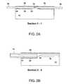
- FIGS. 2A and 2Bshow schematic cross-section views of the device of FIG. 1 along the section lines 1 — 1 and 2 — 2 , respectively.
- FIGS. 3A-3Iillustrate a series of process steps that can be used to form the interconnections of FIG. 1 .
- the microfluidic device 10includes a plurality of interconnections including fluidic interconnections 14 between microcapillary tubing 16 (also termed macrotubing, microtubing or capillary tubing) and a microchannel 18 , and optical interconnections 20 between an optical fiber 22 and the microchannel 18 .
- the fluidic interconnections 14are useful, for example, to couple a fluid into and out from the microchannel 18 ; and the optical interconnections 20 are useful to couple light into and out from the microchannel 18 , for example, to perform an optical analysis (e.g. by absorption, fluorescence or light scattering) of the fluid within the microchannel 18 .
- microchannelrefers to a hollow fluid duct having a width that is generally in the range from about 5 to 500 microns ( ⁇ m), and a height that is generally in the same range as the width.
- fluidis intended to include both liquids and gases.
- FIGS. 2A and 2Bshow enlarged schematic cross-section views along the section lines 1 — 1 and 2 — 2 in FIG. 1, respectively.
- Each interconnection 14 and 20 in FIGS. 2A and 2Bcan be formed by etching an elongate trench 24 below an upper surface of the substrate 12 , with each trench 24 being sized to accept the microcapillary tubing 16 or optical fiber 22 , and with each trench 24 further being connected to an end or side of the microchannel 18 .
- Each trench 24is preferably sized so that a majority or the entirety of the tubing 16 or fiber 22 is located below the surface of the substrate 12 . This aids in photolithography during formation of the external interconnections to the microfluidic device 10 and during the fabrication of other elements on the substrate 12 by maintaining a substantially planar topography for the substrate 12 .
- a portion of the trench 24can be graded (e.g. tapered or stepped) in depth and/or width, if needed, to optimize coupling between the microchannel 18 and the microcapillary tubing 16 or optical fiber 22 .
- Lateral and vertical grading of the end of the trench 24 between the microchannel 18 and the microcapillary tubing 16is shown in FIGS. 1 and 2B.
- the microchannel 18itself can be locally graded in depth or width for coupling to the interconnections 14 and 20 .
- a localized vertical tapering of the microchannel 18can be provided near the ends of the optical fiber 22 terminating at each side or slightly within the microchannel 18 .
- microcapillary tubing 16 and optical fiber 22can each have an outer diameter of, for example, 125-150 ⁇ m or more.
- FIGS. 3A-3Ishow various stages of fabrication of the fluidic interconnection 14 along the section line 2 — 2 in FIG. 2 B.
- the optical interconnection 20can be formed using the same series of process steps used to form the fluidic interconnection 14 .
- both types of interconnections 14 and 20will be fabricated at the same time.
- FIGS. 3A-3Ishow a series of steps that can be used to fabricate the interconnections 14 and 20 of FIG. 1 when one or more microchannels 18 are to be formed at the same time on the substrate 12 using the same processing steps used to form the interconnections 14 and 20 .
- teachings of the present inventioncan also be adapted to form one or more interconnections 14 or 20 on a substrate 12 which already has one or more microchannels 18 formed thereon. Only the essential process steps will be described in detail herein with reference to FIGS. 3A-3I.
- a substrate 12which comprises either a crystalline or a non-crystalline material.
- crystalline materials that can be used for the substrate 12include semiconductors (e.g. silicon, germanium, gallium arsenide) and crystalline quartz.
- Non-crystalline materials that can be used as the substrate 12can include glasses, polymers (i.e. plastics), ceramics, metals (including metal alloys), and fused silica.
- the exact type of substrate 12 to be used according to the present inventionwill depend upon whether the substrate 12 is to be electrically insulating or electrically conducting.
- An electrically-insulating substrate 12comprised of, for example, an undoped semiconductor, glass, ceramic, fused silica, crystalline quartz, or a polymer is preferred for applications requiring high voltages (e.g. 20-100 volts or more) to electrodes located within the microchannel 18 for electrophoresis or electroosmosis.
- a doped semiconductor or metal substrate 12can be used when high voltages are not present on the substrate 12 .
- the substrate 12is patterned to form the microchannel 18 and the trench 24 which includes a graded portion 28 .
- the term “patterning” as used hereinrefers to a series of processing steps including applying a photoresist to the substrate 12 , prebaking the photoresist, aligning the substrate 12 with a photomask, exposing the photoresist through the photomask, developing the photoresist, baking the photoresist to define an etch mask having an opening therethrough that has the lateral shape of the microchannel 18 and trench 24 to be formed in the substrate 12 , etching away the surface of the substrate 12 not protected by the photoresist, and stripping the protected areas of the photoresist so that further processing can take place.
- These processing stepsare well-known in the art and need not be described herein in detail.
- one or more etching stepscan be used to etch downward through the substrate 12 to the depth of the microchannel 18 using a patterned etch mask (not shown) which is formed over the substrate 12 .
- This etchingcan be performed either using a wet etchant or a dry etching process (e.g. reactive ion etching).
- An anisotropic wet etchantcan be used to provide sidewall and bottom surfaces for the microchannel 18 and trench 24 that are defined by crystalline planes in the case of a crystalline substrate material.
- Suitable anisotropic wet etchantsthat can be used for practice of the present invention for a silicon substrate 12 include potassium hydroxide (KOH), tetramethyl ammonium hydroxide (TMAH) or ethylenediamine pyrocatechol (EDP).
- KOHpotassium hydroxide
- TMAHtetramethyl ammonium hydroxide
- EDPethylenediamine pyrocatechol
- hydrofluoric acid (HF)can be used.
- the sidewalls of a crystalline substrate 12will generally be oblique with respect to the surface of the substrate 12 with the exact angle of the sidewalls depending upon the crystalline orientation of the substrate 12 .
- the use of KOH, TMAH or EDP to form the microchannel 18 and trench 24 in a (100) silicon substratewill result in sidewalls that are angled by 55° with respect to the surface of the silicon substrate 12 since the etching will terminate upon reaching ⁇ 111 ⁇ planes of silicon.
- substantially vertical sidewallsi.e.
- an anisotropic dry etching processsuch as reactive ion etching can be used.
- a dry etching processis disclosed, for example, in U.S. Pat. No. 5,501,893 to Laermer, which is incorporated herein by reference.
- an etch mask 30(e.g. comprising photoresist) can be provided over the substrate 12 to fill and protect the microchannel 18 in preparation for further etching of the trench 24 .
- One or more further etching steps as described abovecan then be used to complete formation of the trench 24 .
- a portion 28 of the trench 24can be formed with a vertically tapered bottom surface as shown in FIG. 3C by using an anisotropic wet etching step (e.g. KOH, TMAH or EDP for a silicon substrate 12 with the bottom surface being defined by a ⁇ 111 ⁇ plane of silicon).
- an anisotropic wet etching stepe.g. KOH, TMAH or EDP for a silicon substrate 12 with the bottom surface being defined by a ⁇ 111 ⁇ plane of silicon.
- the bottom surface of the trenchcan be stepped in height near the microchannel 18 by a series of masking and anisotropic dry etching steps.
- the mask 30can be extended to cover the graded region 28 or it can be replaced by another etch mask 32 in preparation for one or more final etching steps to complete formation of the trench 24 in the example of FIG. 1 .
- the final etching step(s)can also produce a vertical end wall 34 of the trench 24 which is useful as a stop to precisely align the microcapillary tubing 16 or optical fiber 22 in the trench 24 .
- the substrate 12 with the completed microchannel 18 and trench 24is shown in FIG. 3E after stripping of the etch mask.
- the completed microchannel 18 and trench 24can be optionally lined with a layer (not shown) of silicon oxynitride which can be advantageous for certain applications such as chromatography or electrophoresis. This can be done by depositing a 0.05- to 3- ⁇ m-thick layer of silicon oxynitride over the substrate 12 and in the microchannel 18 and trench 24 using a high-density plasma deposition process as described hereinafter.
- the microchannel 18 and trench 24can be formed by other processes depending upon the composition of the substrate 12 and the dimensions and dimensional tolerance required for the microchannel 18 and trench 24 . These other processes can include isotropic etching, mechanical abrasion, ion milling or laser ablation. Additionally, the microchannel 18 and trench 24 can be replicated by pressing a master into the substrate 12 . This replication process is particularly useful when the substrate comprises a moldable material such as a ceramic in the green (i.e. unfired) state, a glass or polymer heated above a softening temperature, or a metal at room temperature or at an elevated temperature.
- a moldable materialsuch as a ceramic in the green (i.e. unfired) state, a glass or polymer heated above a softening temperature, or a metal at room temperature or at an elevated temperature.
- microchannels 18will have already been formed on the substrate 12 so that only the interconnections 14 and 20 need be formed on the substrate 12 .
- the process used for forming the trench 24can be selected for compatibility with the already existing microchannels 18 .
- the microcapillary tubing 16is attached to the substrate 12 in the trench 24 using an adhesive 26 that is preferably disposed in the trench 24 prior to insertion of the microcapillary tubing 16 .
- the adhesive 26can be, for example, an epoxy that is curable using ultraviolet (UV) light.
- the adhesive 26can be a polymer (e.g. silicone rubber) which is impervious to a fluid to be provided to the microchannel 18 and also to a solvent (e.g. acetone) that is used during a later step in forming the interconnections 14 and 20 .
- the adhesive 26can be disposed in a central portion of each trench 24 prior to insertion of the microcapillary tubing 16 or optical fiber 22 , and preferably does not obscure the bore 30 of the tubing 16 or the end of the optical fiber 22 . Any of the adhesive 26 that extends above the upper surface of the substrate 12 is preferably removed either before or after curing of the adhesive 26 to maintain a planar topography for the substrate 12 .
- a sacrificial material 36e.g. photoresist such as a positive tone thick photoresist, or a photodefinable polymer such as a photodefinable polyimide
- a sacrificial material 36can be spun on over the substrate 12 to fill in the microchannel 18 and the graded portion 28 , with the sacrificial material 36 then being removed from the remainder of the substrate 12 .
- This step of removing any excess sacrificial materialcan be performed using photolithographic patterning, developing. and stripping as known to the art.
- an oxygen plasma cleansing stepcan be used to remove any photoresist residue remaining on the upper surface of the substrate 12 , and on the microcapillary tubing 16 and optical fibers 22 .
- the sacrificial material 36can, however, extend partway (e.g. by a few microns) over the top of the microcapillary tubing 16 and optical fiber 22 near the graded portion 28 to ensure that the ends of the tubing 16 and fibers 22 are covered. Removing the sacrificial material 36 from the majority of the surfaces of the microcapillary tubing 16 and optical fiber 22 is important since these surfaces will be sealed using a deposited fluid-tight covering 38 as described hereinafter. If the sacrificial material 36 extends partway into the bore 40 of the microcapillary tubing 16 as shown in FIG. 3G, this is not problematic since the sacrificial material 36 will later be removed using a solvent.
- a fluid-tight covering layer 38is blanket deposited over the substrate 12 to close the microchannels 18 and the trench 24 and to form a fluid-tight seal between the microchannels 18 and the microcapillary tubing 16 and optical fibers 22 .
- the covering layer 38comprises silicon oxynitride that can be deposited by a high-density plasma deposition process as disclosed in U.S. Pat. No. 6,096,656 to Matzke et al, which is incorporated herein by reference.
- This high-density plasma deposition processutilizes a plasma having a relatively high electron, ion and neutral radical density and flux (e.g.
- Such a plasmacan be obtained, for example, with an electron-cyclotron resonance (ECR) plasma deposition system, or with an inductively-coupled plasma (ICP) deposition system.
- ECRelectron-cyclotron resonance
- ICPinductively-coupled plasma
- the ECR plasma deposition systemwhich is used to deposit the covering layer 38 according to the present invention, utilizes microwaves to generate a high-density plasma from supplied source gases, and a magnetic field to keep electrons circulating in the plasma to produce a high electron density and to control beam collimation. No additional substrate heating is necessary for the ECR plasma deposition system so that deposition of the covering layer 38 can be performed at a low temperature of about 100° C. or less.
- the use of a relatively low deposition temperatureis advantageous since this allows the use of photoresist or a photodefinable polymer as the sacrificial material 36 while minimizing potential damage to the sacrificial material 36 by polymerization.
- the ECR plasma deposition systemallows the use of a low substrate bias voltage of 100 volts or less.
- the bias voltageneed not be constant during the entire deposition of the covering layer 38 .
- a bias voltage in the range of 50-100 voltscan be used for a short duration (e.g. 15 seconds) upon commencing deposition of the covering layer 38 to improve adhesion of the covering layer 38 to the substrate 12 , to the microcapillary tubing 16 and optical fibers 22 , and to any microchannels 18 pre-existing upon the substrate 12 .
- the bias voltagecan be reduced to a low value (e.g.
- the bias voltagecan be maintained in the range of 20-100 volts during deposition of part or all of the covering layer 38 to densify the covering layer 38 .
- the covering layer 38can be deposited using an inductively-coupled plasma deposition system as known to the art.
- An inductively-coupled plasma deposition systemutilizes a radio-frequency (rf) coil to produce a plasma having characteristics similar to the ECR system described above.
- Inductively-coupled plasma deposition systemsare also referred to as transformer-coupled plasma (TCP) systems or as rf induction (RFI) systems.
- the covering layer 38 in FIG. 3Hcan comprise a single layer of silicon oxynitride, or alternately a layer of silicon oxynitride with a layer of silicon dioxide deposited on one or both sides of the silicon oxynitride layer.
- the use of silicon oxynitride for the covering layer 38is advantageous since this material is resistant to cracking, and is resilient.
- the provision of a silicon dioxide layer on one or both sides of the silicon oxynitride layeris useful as a barrier layer since the silicon oxynitride can be attacked by moisture and other chemicals (e.g. aqueous, ethanolic or methanolic fluids) present within the microchannel 18 , or in the environment.
- the ECR systemcan be operated at a microwave power level of generally 80-400 W, and preferably at either 125 or 385 W, with the microwave frequency generally being 2.45 GHz.
- the silicon oxynitride and silicon dioxide layerscan be deposited during a single run without turning off the plasma. This can be done by switching between different source gases including silane (SiH 4 ) and oxygen-and nitrogen-containing gases such as nitrogen (N 2 ), oxygen (O 2 ) and nitrous oxide (N 2 O).
- Argon (Ar)can additionally be added to the plasma.
- the ECR high-density plasmacan be operated at a pressure of typically 15-30 mTorr, and preferably about 20 mTorr.
- Flow rates for the source gasescan be in the range of 5-50 standard-cubic-centimeters-per-minute (sccm) silane, 5-50 sccm of the oxygen-and nitrogen-containing source gases, and 0-20 sccm argon.
- the nitrogen-containing source gascan be switched off to deposit each silicon dioxide layer, and switched on again to deposit the silicon oxynitride layer.
- Deposition of the covering layer 38an be performed as previously described with a bias voltage provided to the substrate 12 , and with no substrate heating.
- the deposition rate of the silicon dioxide and silicon oxynitride layerscan be in the range of 5-400 nanometers/ minute using an ECR plasma.
- the thickness of the silicon oxynitridecan be, for example, about 2-5 ⁇ m or more, with a thickness of about 5 ⁇ m generally being used when the size of the trench 24 is about 250 ⁇ m.
- the silicon oxynitride layercan be, for example, 1.2 ⁇ m thick, with each silicon dioxide layer being 0.4 ⁇ m thick for use with microcapillary tubing 16 and optical fibers 22 each having an outer diameter in the range of 125-150 ⁇ m.
- the ECR-deposited silicon oxynitridecan comprise, for example, 40 at. % silicon, 36 at. % nitrogen, 12 at. % oxygen and 12 at. % hydrogen.
- the silicon oxynitride deposited to form the covering layer 38 according to the present inventioncan comprise a partially hydrogenated silicon oxynitride having a composition Si w O x N y H z , with w being in the range 25-65 at. % silicon, x being in the range 5-40 at. % oxygen, y being in the range 10-40 at. % nitrogen, and z being in the range 0-25 at. % hydrogen.
- the exact composition of the silicon oxynitridewill depend upon the operating parameters of the high-density plasma deposition system, and on whether or not an annealing step is provided to densify the silicon oxynitride thereby lowering its hydrogen content.
- the same source gases abovecan be used, and the flow rates and plasma parameters can be adjusted to provide a composition for the silicon oxynitride within the above range as determined from Rutherford backscattering measurements and/or index of refraction measurements.
- the silicon oxynitride and silicon dioxide layersare preferably deposited without switching off the plasma to obtain the highest quality covering layer 38 , and to prevent any potential cracking of the silicon dioxide layers therein.
- the sacrificial material 36is removed from the microchannel 18 and trench 24 to complete formation of the microchannel 18 and the interconnections 14 and 20 .
- the covering layer 38provides a fluid-tight seal between the microcapillary tubing 16 and optical fibers 22 and the microchannel 18 , and also further adheres the tubing 16 and fibers 22 to the surrounding substrate 12 .
- the sacrificial material 36 in FIG. 3Hcan be removed by dissolution using a suitable solvent such as acetone, n-methyl pyrrolidone (NMP) or a commercial photoresist stripping solution. This can be done by contacting the sacrificial material 36 with the solvent provided through the microcapillary tubing 16 , through an open end of the microchannel 18 , or through a plurality of micron-sized holes (not shown) formed (e.g. using reactive ion etching or laser ablation) down through the covering layer 38 to expose the sacrificial material 36 . Removal of the sacrificial material 36 using the solvent can be performed over a period of up to several hours or over night, with or without agitation or heating. Once the sacrificial material 36 has been removed, the covering layer 38 can be densified, if desired, by heating to a high temperature of 400° C. or more for about 30 seconds in a rapid thermal annealer.
- a suitable solventsuch as acetone
- the holescan be plugged by depositing one or more additional material layers (not shown) over the substrate 12 .
- additional layerscan comprise, for example, silicon oxynitride and/or silicon dioxide deposited using the ECR or ICP deposition system as described previously.
- the additional layerscan comprise an elastomer, a photoactivated epoxy, a commercial potting compound, a polyimide, a spin-on glass or a deposited metallization.
- These additional material layerscan be useful to further strengthen the microchannel 18 and the interconnections 14 and 20 , and can be used for this purpose even if no holes are formed through the covering layer 38 .
- the completed microfluidic device 10 having one or more fluidic interconnections 14 and/or optical interconnections 20is as shown in FIGS. 1 and 2A and 2 B.
- the existing microchannels 18can be covered, if needed, with an etch mask or other protection layer during formation of the interconnections 14 and 20 .
- the sacrificial material 36 in FIG. 3Gwill be largely confined to the graded region 28 or to a small (e.g. micron-sized) gap between the microcapillary tubing 16 or optical fiber 22 and the microchannel 18 , and will be more easily removable using the process described previously.
- microfluidic devices 10with arbitrary microchannel shapes and cross sections, and with multiple intersecting microchannels 18 can be formed according to the present invention so that a fluid can be introduced into and out of the microchannels 18 using one or more fluidic interconnections 14 according to the present invention, and with optional coupling of light (e.g. from a laser, light-emitting diode, or a lamp) into and out from the microchannels 18 by one or more optical interconnections 20 for analysis of particular analytes in the fluid.
- lighte.g. from a laser, light-emitting diode, or a lamp
- optical interconnections 20for analysis of particular analytes in the fluid.
Landscapes
- Chemical & Material Sciences (AREA)
- Chemical Kinetics & Catalysis (AREA)
- Health & Medical Sciences (AREA)
- Clinical Laboratory Science (AREA)
- Engineering & Computer Science (AREA)
- Analytical Chemistry (AREA)
- Dispersion Chemistry (AREA)
- Organic Chemistry (AREA)
- General Health & Medical Sciences (AREA)
- Hematology (AREA)
- Microelectronics & Electronic Packaging (AREA)
- Computer Hardware Design (AREA)
- Ceramic Engineering (AREA)
- Life Sciences & Earth Sciences (AREA)
- General Chemical & Material Sciences (AREA)
- Geochemistry & Mineralogy (AREA)
- Materials Engineering (AREA)
- Micromachines (AREA)
Abstract
Description
This invention was made with Government support under Contract No. DE-AC04-94AL85000 awarded by the U.S. Department of Energy. The Government has certain rights in the invention.
The present invention relates generally to microfluidic devices having one or more microchannels formed on a substrate, and specifically to optical or fluid interconnections formed to microfluidic devices, to microfluidic devices incorporating such interconnections, and to a process for forming the same.
Microfluidic devices are being developed for many applications including micro analysis systems, micromechanical actuators, localized or global substrate cooling, and ink-jet printing. Micro analysis systems which utilize microminiature fluid channels include liquid and gas chromatography, electrophoresis, free-flow fractionation, and polmerase chain reaction.
Conventional methods for forming interconnections to microfluidic devices are largely based on piece-part assembly with microcapillary tubing being oriented perpendicular to a backside of a substrate containing the microfluidic device and connected to a microchannel through a hole formed through the substrate (see e.g. U.S. Pat. No. 6,096,656 to Matzke et al, which is incorporated herein by reference). The microcapillary tubing is attached to the substrate using an adhesive which is disposed in the hole through the substrate. In some cases, the microcapillary tubing can be initially attached to small pieces of glass having machined thru-holes which are then attached to the backside of the substrate using an adhesive or anodic bonding.
The present invention provides an improvement over the prior art by forming external interconnections using microcapillary tubing or optical fibers which are oriented substantially parallel to an upper surface of the substrate whereon the microfluidic device is formed.
The present invention allows the external interconnections to be precisely aligned with one or more microchannels within a microfluidic device, and to be formed during or after formation of the microchannels using processes which are compatible with formation of the microchannels.
These and other advantages of the present invention will become evident to those skilled in the art.
The present invention relates to a microfluidic device comprising a substrate having at least one microchannel formed therein, with at least one external interconnection to the microchannel being formed substantially parallel to a surface of the substrate by a microcapillary tubing or an optical fiber located within an elongate trench formed in the substrate proximate to the microchannel and connected thereto, and with a covering layer comprising silicon oxynitride being deposited over the substrate to cover the trench and thereby adhere, at least in part, the microcapillary tubing or optical fiber to the substrate. The microcapillary tubing or optical fiber is generally further adhered to the substrate by an adhesive disposed within the trench. The covering layer also forms a fluid-tight seal between the microchannel and the external interconnection which is sealed at its sides and bottom to the trench with the adhesive.
The trench can be formed with sidewalls that are oriented substantially perpendicular to the surface of the substrate, or at oblique angles to the surface. One end of the trench proximate to the microchannel can be optionally graded to accommodate microcapillary tubing which is larger than the microchannel.
A barrier layer (e.g. comprising silicon dioxide) can be provided on one or both sides of the silicon oxynitride layer for improved resistance to moisture or chemical attack.
The substrate can comprise a material such as a semiconductor (e.g. silicon), crystalline quartz, fused silica, glass, ceramic, a polymer or a metal. In some instances an electrically-insulating substrate is preferred, for example, when high voltages are provided to the microfluidic device to provide an electrophoretic, electrokinetic or electroosmotic flow therein.
The present invention further relates to an optical or fluidic interconnection to a microchannel formed in a substrate. The interconnection comprises an elongate trench formed in the substrate proximate to the microchannel and connected thereto, with the trench being aligned substantially parallel to a surface of the substrate wherein the microchannel is formed. The interconnection further comprises a microfluidic tubing or optical fiber located within the trench and adhered to the sides and bottom of the trench with an adhesive disposed in the trench, and a fluid-tight covering formed over at least a portion of the trench, with the fluid-tight covering comprising a layer of silicon oxynitride.
The interconnection can be formed to microfluidic devices fabricated on many different types of substrates as described above; and the trench can be formed with sidewalls that are substantially perpendicular to the surface of the substrate, or oriented at oblique angles thereto. The trench can also be graded at one end thereof proximate to the microchannel, if needed.
A barrier layer can be provided on one or both sides of the silicon oxynitride layer to improve the resistance to moisture and prevent chemical attack (e.g. corrosion). The barrier layer, if used, generally comprises silicon dioxide.
The present invention also relates to a method for forming an interconnection to a microchannel on a substrate that comprises forming (e.g. by etching) an elongate trench below a surface of the substrate near an edge thereof proximate to the microchannel, with the trench being sized to receive one end of a microcapillary tubing or an optical fiber, and with one end of the trench being connected to the microchannel; adhering the end of the microcapillary tubing or optical fiber within the trench with an adhesive (e.g. an epoxy which can be cured using ultraviolet light); depositing a sacrificial material (e.g. a photoresist or a photodefinable polymer) within a portion of the trench not occupied by the microcapillary tubing or optical fiber; depositing a layer of silicon oxynitride over the surface of the substrate, with the layer of silicon oxynitride forming a fluid-tight covering over the trench and over the end of the microcapillary tubing or optical fiber located within the trench; and removing (e.g. by dissolution using a solvent) the sacrificial material from the trench. This method is particularly useful for forming interconnections to microfluidic devices when the microchannel is pre-existing on the substrate. An optional step can be provided for forming a barrier layer on one or both sides of the silicon oxynitride layer, if needed, to improve resistance to moisture and chemical attack.
In some instances, the present invention can be used to form the interconnections and microchannels at the same time and using the same series of process steps. This can be done with a simple modification of the above method by forming a microchannel on the substrate, and forming at least one elongate trench connected to the microchannel, with each trench being located near an edge of the substrate and being sized to receive one end of a microcapillary tubing or optical fiber; adhering the end of the microcapillary tubing or optical fiber within the trench with an adhesive; depositing a sacrificial material within the microchannel and within a portion of the trench not occupied by the microcapillary tubing or optical fiber; depositing a layer of silicon oxynitride over the surface of the substrate, with the layer of silicon oxynitride forming a fluid-tight covering over the microchannel and the trench, and over the end of the microcapillary tubing or optical fiber located within the trench; and removing the sacrificial material from the microchannel and trench.
Additional advantages and novel features of the invention will become apparent to those skilled in the art upon examination of the following detailed description thereof when considered in conjunction with the accompanying drawings. The advantages of the invention can be realized and attained by means of the instrumentalities and combinations particularly pointed out in the appended claims.
The accompanying drawings, which are incorporated into and form a part of the specification, illustrate several aspects of the present invention and, together with the description, serve to explain the principles of the invention. The drawings are only for the purpose of illustrating preferred embodiments of the invention and are not to be construed as limiting the invention. In the drawings:
FIG. 1 schematically illustrates in plan view a microfluidic device having a plurality of optical and fluidic interconnections formed according to the present invention.
FIGS. 2A and 2B show schematic cross-section views of the device of FIG. 1 along thesection lines 1—1 and2—2, respectively.
FIGS. 3A-3I illustrate a series of process steps that can be used to form the interconnections of FIG.1.
Referring to FIG. 1, there is shown a schematic plan view of an example of amicrofluidic device 10 formed on asubstrate 12 according to the present invention. Themicrofluidic device 10 includes a plurality of interconnections includingfluidic interconnections 14 between microcapillary tubing16 (also termed macrotubing, microtubing or capillary tubing) and amicrochannel 18, andoptical interconnections 20 between anoptical fiber 22 and themicrochannel 18. Thefluidic interconnections 14 are useful, for example, to couple a fluid into and out from themicrochannel 18; and theoptical interconnections 20 are useful to couple light into and out from themicrochannel 18, for example, to perform an optical analysis (e.g. by absorption, fluorescence or light scattering) of the fluid within themicrochannel 18.
As defined herein, the term “microchannel” refers to a hollow fluid duct having a width that is generally in the range from about 5 to 500 microns (μm), and a height that is generally in the same range as the width. The term “fluid” is intended to include both liquids and gases.
FIGS. 2A and 2B show enlarged schematic cross-section views along thesection lines 1—1 and2—2 in FIG. 1, respectively. Eachinterconnection elongate trench 24 below an upper surface of thesubstrate 12, with eachtrench 24 being sized to accept themicrocapillary tubing 16 oroptical fiber 22, and with eachtrench 24 further being connected to an end or side of themicrochannel 18. Eachtrench 24 is preferably sized so that a majority or the entirety of thetubing 16 orfiber 22 is located below the surface of thesubstrate 12. This aids in photolithography during formation of the external interconnections to themicrofluidic device 10 and during the fabrication of other elements on thesubstrate 12 by maintaining a substantially planar topography for thesubstrate 12.
A portion of thetrench 24 can be graded (e.g. tapered or stepped) in depth and/or width, if needed, to optimize coupling between themicrochannel 18 and themicrocapillary tubing 16 oroptical fiber 22. Lateral and vertical grading of the end of thetrench 24 between themicrochannel 18 and themicrocapillary tubing 16 is shown in FIGS. 1 and 2B. Alternately, themicrochannel 18 itself can be locally graded in depth or width for coupling to theinterconnections microchannel 18 can be provided near the ends of theoptical fiber 22 terminating at each side or slightly within themicrochannel 18. This is useful, for example, for coupling light from anoptical fiber 22 into and out from themicrochannel 18 when an outer diameter of thefiber 22 exceeds the depth of a majority of themicrochannel 18. Themicrocapillary tubing 16 andoptical fiber 22 can each have an outer diameter of, for example, 125-150 μm or more.
Formation of theinterconnections fluidic interconnection 14 along thesection line 2—2 in FIG.2B. Those skilled in the art will understand that theoptical interconnection 20 can be formed using the same series of process steps used to form thefluidic interconnection 14. Generally, both types ofinterconnections
FIGS. 3A-3I show a series of steps that can be used to fabricate theinterconnections more microchannels 18 are to be formed at the same time on thesubstrate 12 using the same processing steps used to form theinterconnections more interconnections substrate 12 which already has one ormore microchannels 18 formed thereon. Only the essential process steps will be described in detail herein with reference to FIGS. 3A-3I.
In FIG. 3A, asubstrate 12 is provided which comprises either a crystalline or a non-crystalline material. In particular, crystalline materials that can be used for thesubstrate 12 include semiconductors (e.g. silicon, germanium, gallium arsenide) and crystalline quartz. Non-crystalline materials that can be used as thesubstrate 12 can include glasses, polymers (i.e. plastics), ceramics, metals (including metal alloys), and fused silica. The exact type ofsubstrate 12 to be used according to the present invention will depend upon whether thesubstrate 12 is to be electrically insulating or electrically conducting. An electrically-insulatingsubstrate 12 comprised of, for example, an undoped semiconductor, glass, ceramic, fused silica, crystalline quartz, or a polymer is preferred for applications requiring high voltages (e.g. 20-100 volts or more) to electrodes located within themicrochannel 18 for electrophoresis or electroosmosis. Alternately, a doped semiconductor ormetal substrate 12 can be used when high voltages are not present on thesubstrate 12.
In FIGS. 3B-3D, thesubstrate 12 is patterned to form themicrochannel 18 and thetrench 24 which includes a gradedportion 28. When themicrochannel 18 andtrench 24 are formed by photolithography and etching, the term “patterning” as used herein refers to a series of processing steps including applying a photoresist to thesubstrate 12, prebaking the photoresist, aligning thesubstrate 12 with a photomask, exposing the photoresist through the photomask, developing the photoresist, baking the photoresist to define an etch mask having an opening therethrough that has the lateral shape of themicrochannel 18 andtrench 24 to be formed in thesubstrate 12, etching away the surface of thesubstrate 12 not protected by the photoresist, and stripping the protected areas of the photoresist so that further processing can take place. These processing steps are well-known in the art and need not be described herein in detail. To fabricate themicrochannel 18 andtrench 24 with different depths as shown in FIGS. 3B-3D, multiple etch masks are generally required.
In FIG. 3B, one or more etching steps can be used to etch downward through thesubstrate 12 to the depth of themicrochannel 18 using a patterned etch mask (not shown) which is formed over thesubstrate 12. This etching can be performed either using a wet etchant or a dry etching process (e.g. reactive ion etching). An anisotropic wet etchant can be used to provide sidewall and bottom surfaces for themicrochannel 18 andtrench 24 that are defined by crystalline planes in the case of a crystalline substrate material. Suitable anisotropic wet etchants that can be used for practice of the present invention for asilicon substrate 12 include potassium hydroxide (KOH), tetramethyl ammonium hydroxide (TMAH) or ethylenediamine pyrocatechol (EDP). For acrystalline quartz substrate 12, hydrofluoric acid (HF) can be used.
When forming themicrochannel 18 andtrench 24 using an anisotropic wet etchant, the sidewalls of acrystalline substrate 12 will generally be oblique with respect to the surface of thesubstrate 12 with the exact angle of the sidewalls depending upon the crystalline orientation of thesubstrate 12. For example, the use of KOH, TMAH or EDP to form themicrochannel 18 andtrench 24 in a (100) silicon substrate will result in sidewalls that are angled by 55° with respect to the surface of thesilicon substrate 12 since the etching will terminate upon reaching {111} planes of silicon. To form themicrochannel 18 andtrench 24 with substantially vertical sidewalls (i.e. perpendicular to the surface of the substrate12), an anisotropic dry etching process such as reactive ion etching can be used. Such a dry etching process is disclosed, for example, in U.S. Pat. No. 5,501,893 to Laermer, which is incorporated herein by reference.
In FIG. 3C, when it is necessary to etch thetrench 24 deeper than themicrochannel 18, an etch mask30 (e.g. comprising photoresist) can be provided over thesubstrate 12 to fill and protect themicrochannel 18 in preparation for further etching of thetrench 24. One or more further etching steps as described above can then be used to complete formation of thetrench 24. Aportion 28 of thetrench 24 can be formed with a vertically tapered bottom surface as shown in FIG. 3C by using an anisotropic wet etching step (e.g. KOH, TMAH or EDP for asilicon substrate 12 with the bottom surface being defined by a {111} plane of silicon). Alternately, the bottom surface of the trench can be stepped in height near themicrochannel 18 by a series of masking and anisotropic dry etching steps.
In FIG. 3D, themask 30 can be extended to cover the gradedregion 28 or it can be replaced by anotheretch mask 32 in preparation for one or more final etching steps to complete formation of thetrench 24 in the example of FIG.1. The final etching step(s) can also produce avertical end wall 34 of thetrench 24 which is useful as a stop to precisely align themicrocapillary tubing 16 oroptical fiber 22 in thetrench 24.
Thesubstrate 12 with the completedmicrochannel 18 andtrench 24 is shown in FIG. 3E after stripping of the etch mask. The completedmicrochannel 18 andtrench 24 can be optionally lined with a layer (not shown) of silicon oxynitride which can be advantageous for certain applications such as chromatography or electrophoresis. This can be done by depositing a 0.05- to 3-μm-thick layer of silicon oxynitride over thesubstrate 12 and in themicrochannel 18 andtrench 24 using a high-density plasma deposition process as described hereinafter.
Those skilled in the art will understand that themicrochannel 18 andtrench 24 can be formed by other processes depending upon the composition of thesubstrate 12 and the dimensions and dimensional tolerance required for themicrochannel 18 andtrench 24. These other processes can include isotropic etching, mechanical abrasion, ion milling or laser ablation. Additionally, themicrochannel 18 andtrench 24 can be replicated by pressing a master into thesubstrate 12. This replication process is particularly useful when the substrate comprises a moldable material such as a ceramic in the green (i.e. unfired) state, a glass or polymer heated above a softening temperature, or a metal at room temperature or at an elevated temperature. The term “replication” as used herein is intended to include any type of molding operation including injection molding, stamping, embossing or casting with or without heating. In some instances, one ormore microchannels 18 will have already been formed on thesubstrate 12 so that only theinterconnections substrate 12. In this case, the process used for forming thetrench 24 can be selected for compatibility with the already existingmicrochannels 18.
In FIG. 3F, themicrocapillary tubing 16 is attached to thesubstrate 12 in thetrench 24 using an adhesive26 that is preferably disposed in thetrench 24 prior to insertion of themicrocapillary tubing 16. The adhesive26 can be, for example, an epoxy that is curable using ultraviolet (UV) light. Alternately, the adhesive26 can be a polymer (e.g. silicone rubber) which is impervious to a fluid to be provided to themicrochannel 18 and also to a solvent (e.g. acetone) that is used during a later step in forming theinterconnections trench 24 prior to insertion of themicrocapillary tubing 16 oroptical fiber 22, and preferably does not obscure thebore 30 of thetubing 16 or the end of theoptical fiber 22. Any of the adhesive26 that extends above the upper surface of thesubstrate 12 is preferably removed either before or after curing of the adhesive26 to maintain a planar topography for thesubstrate 12.
In FIG. 3G, once themicrocapillary tubing 16 andoptical fibers 22 are in place on thesubstrate 12, one or more layers of a sacrificial material36 (e.g. photoresist such as a positive tone thick photoresist, or a photodefinable polymer such as a photodefinable polyimide) can be spun on over thesubstrate 12 to fill in themicrochannel 18 and the gradedportion 28, with thesacrificial material 36 then being removed from the remainder of thesubstrate 12. This step of removing any excess sacrificial material can be performed using photolithographic patterning, developing. and stripping as known to the art.
Additionally, an oxygen plasma cleansing step can be used to remove any photoresist residue remaining on the upper surface of thesubstrate 12, and on themicrocapillary tubing 16 andoptical fibers 22. Thesacrificial material 36 can, however, extend partway (e.g. by a few microns) over the top of themicrocapillary tubing 16 andoptical fiber 22 near the gradedportion 28 to ensure that the ends of thetubing 16 andfibers 22 are covered. Removing thesacrificial material 36 from the majority of the surfaces of themicrocapillary tubing 16 andoptical fiber 22 is important since these surfaces will be sealed using a deposited fluid-tight covering 38 as described hereinafter. If thesacrificial material 36 extends partway into thebore 40 of themicrocapillary tubing 16 as shown in FIG. 3G, this is not problematic since thesacrificial material 36 will later be removed using a solvent.
In FIG. 3H, a fluid-tight covering layer 38 is blanket deposited over thesubstrate 12 to close themicrochannels 18 and thetrench 24 and to form a fluid-tight seal between the microchannels18 and themicrocapillary tubing 16 andoptical fibers 22. Thecovering layer 38 comprises silicon oxynitride that can be deposited by a high-density plasma deposition process as disclosed in U.S. Pat. No. 6,096,656 to Matzke et al, which is incorporated herein by reference. This high-density plasma deposition process utilizes a plasma having a relatively high electron, ion and neutral radical density and flux (e.g. an electron density of 1011-5×10¹³electrons/cm3and a positive ion flux of 1-50 mA/cm2). Such a plasma can be obtained, for example, with an electron-cyclotron resonance (ECR) plasma deposition system, or with an inductively-coupled plasma (ICP) deposition system.
The ECR plasma deposition system, which is used to deposit thecovering layer 38 according to the present invention, utilizes microwaves to generate a high-density plasma from supplied source gases, and a magnetic field to keep electrons circulating in the plasma to produce a high electron density and to control beam collimation. No additional substrate heating is necessary for the ECR plasma deposition system so that deposition of thecovering layer 38 can be performed at a low temperature of about 100° C. or less. The use of a relatively low deposition temperature is advantageous since this allows the use of photoresist or a photodefinable polymer as thesacrificial material 36 while minimizing potential damage to thesacrificial material 36 by polymerization.
Additionally, the ECR plasma deposition system allows the use of a low substrate bias voltage of 100 volts or less. The bias voltage need not be constant during the entire deposition of thecovering layer 38. For example, a bias voltage in the range of 50-100 volts can be used for a short duration (e.g. 15 seconds) upon commencing deposition of thecovering layer 38 to improve adhesion of thecovering layer 38 to thesubstrate 12, to themicrocapillary tubing 16 andoptical fibers 22, and to anymicrochannels 18 pre-existing upon thesubstrate 12. The bias voltage can be reduced to a low value (e.g. 5 volts) to prevent etch-back during deposition of the remainder of thecovering layer 38, or alternately, the bias voltage can be maintained in the range of 20-100 volts during deposition of part or all of thecovering layer 38 to densify thecovering layer 38.
Alternately, the coveringlayer 38 can be deposited using an inductively-coupled plasma deposition system as known to the art. An inductively-coupled plasma deposition system utilizes a radio-frequency (rf) coil to produce a plasma having characteristics similar to the ECR system described above. Inductively-coupled plasma deposition systems are also referred to as transformer-coupled plasma (TCP) systems or as rf induction (RFI) systems.
Thecovering layer 38 in FIG. 3H can comprise a single layer of silicon oxynitride, or alternately a layer of silicon oxynitride with a layer of silicon dioxide deposited on one or both sides of the silicon oxynitride layer. The use of silicon oxynitride for thecovering layer 38 is advantageous since this material is resistant to cracking, and is resilient. The provision of a silicon dioxide layer on one or both sides of the silicon oxynitride layer is useful as a barrier layer since the silicon oxynitride can be attacked by moisture and other chemicals (e.g. aqueous, ethanolic or methanolic fluids) present within themicrochannel 18, or in the environment.
To form thecovering layer 38 using an ECR plasma deposition system, the ECR system can be operated at a microwave power level of generally 80-400 W, and preferably at either 125 or 385 W, with the microwave frequency generally being 2.45 GHz. The silicon oxynitride and silicon dioxide layers can be deposited during a single run without turning off the plasma. This can be done by switching between different source gases including silane (SiH4) and oxygen-and nitrogen-containing gases such as nitrogen (N2), oxygen (O2) and nitrous oxide (N2O). Argon (Ar) can additionally be added to the plasma.
The ECR high-density plasma can be operated at a pressure of typically 15-30 mTorr, and preferably about 20 mTorr. Flow rates for the source gases can be in the range of 5-50 standard-cubic-centimeters-per-minute (sccm) silane, 5-50 sccm of the oxygen-and nitrogen-containing source gases, and 0-20 sccm argon. The nitrogen-containing source gas can be switched off to deposit each silicon dioxide layer, and switched on again to deposit the silicon oxynitride layer. Deposition of thecovering layer 38 an be performed as previously described with a bias voltage provided to thesubstrate 12, and with no substrate heating. The deposition rate of the silicon dioxide and silicon oxynitride layers can be in the range of 5-400 nanometers/ minute using an ECR plasma.
When the covering layer comprises silicon oxynitride alone, the thickness of the silicon oxynitride can be, for example, about 2-5 μm or more, with a thickness of about 5 μm generally being used when the size of thetrench 24 is about 250 μm. When the silicon oxynitride layer is sandwiched between a pair of silicon dioxide layers, the silicon oxynitride layer can be, for example, 1.2 μm thick, with each silicon dioxide layer being 0.4 μm thick for use withmicrocapillary tubing 16 andoptical fibers 22 each having an outer diameter in the range of 125-150 μm.
The ECR-deposited silicon oxynitride can comprise, for example, 40 at. % silicon, 36 at. % nitrogen, 12 at. % oxygen and 12 at. % hydrogen. In general, the silicon oxynitride deposited to form thecovering layer 38 according to the present invention can comprise a partially hydrogenated silicon oxynitride having a composition SiwOxNyHz, with w being in the range 25-65 at. % silicon, x being in the range 5-40 at. % oxygen, y being in the range 10-40 at. % nitrogen, and z being in the range 0-25 at. % hydrogen. The exact composition of the silicon oxynitride will depend upon the operating parameters of the high-density plasma deposition system, and on whether or not an annealing step is provided to densify the silicon oxynitride thereby lowering its hydrogen content.
In forming thecovering layer 38 comprising silicon oxynitride with or without added silicon dioxide barrier layers using an ICP plasma source, the same source gases above can be used, and the flow rates and plasma parameters can be adjusted to provide a composition for the silicon oxynitride within the above range as determined from Rutherford backscattering measurements and/or index of refraction measurements. As described above, the silicon oxynitride and silicon dioxide layers are preferably deposited without switching off the plasma to obtain the highestquality covering layer 38, and to prevent any potential cracking of the silicon dioxide layers therein.
In FIG. 3I, thesacrificial material 36 is removed from themicrochannel 18 andtrench 24 to complete formation of themicrochannel 18 and theinterconnections covering layer 38 provides a fluid-tight seal between themicrocapillary tubing 16 andoptical fibers 22 and themicrochannel 18, and also further adheres thetubing 16 andfibers 22 to the surroundingsubstrate 12.
Thesacrificial material 36 in FIG. 3H can be removed by dissolution using a suitable solvent such as acetone, n-methyl pyrrolidone (NMP) or a commercial photoresist stripping solution. This can be done by contacting thesacrificial material 36 with the solvent provided through themicrocapillary tubing 16, through an open end of themicrochannel 18, or through a plurality of micron-sized holes (not shown) formed (e.g. using reactive ion etching or laser ablation) down through thecovering layer 38 to expose thesacrificial material 36. Removal of thesacrificial material 36 using the solvent can be performed over a period of up to several hours or over night, with or without agitation or heating. Once thesacrificial material 36 has been removed, the coveringlayer 38 can be densified, if desired, by heating to a high temperature of 400° C. or more for about 30 seconds in a rapid thermal annealer.
When holes have been formed through thecovering layer 38 to remove thesacrificial material 36, the holes can be plugged by depositing one or more additional material layers (not shown) over thesubstrate 12. These additional layers can comprise, for example, silicon oxynitride and/or silicon dioxide deposited using the ECR or ICP deposition system as described previously. Alternately, the additional layers can comprise an elastomer, a photoactivated epoxy, a commercial potting compound, a polyimide, a spin-on glass or a deposited metallization. These additional material layers can be useful to further strengthen themicrochannel 18 and theinterconnections covering layer 38.
The completedmicrofluidic device 10 having one or morefluidic interconnections 14 and/oroptical interconnections 20 is as shown in FIGS. 1 and 2A and2B. In other embodiments of the present invention where one or moreexternal interconnections 14 and/or20 are to be formed to one ormore microchannels 18 already existing on asubstrate 12, the existingmicrochannels 18 can be covered, if needed, with an etch mask or other protection layer during formation of theinterconnections sacrificial material 36 in FIG. 3G will be largely confined to the gradedregion 28 or to a small (e.g. micron-sized) gap between themicrocapillary tubing 16 oroptical fiber 22 and themicrochannel 18, and will be more easily removable using the process described previously.
Those skilled in the art will understand thatmicrofluidic devices 10 with arbitrary microchannel shapes and cross sections, and with multiple intersectingmicrochannels 18 can be formed according to the present invention so that a fluid can be introduced into and out of themicrochannels 18 using one or morefluidic interconnections 14 according to the present invention, and with optional coupling of light (e.g. from a laser, light-emitting diode, or a lamp) into and out from themicrochannels 18 by one or moreoptical interconnections 20 for analysis of particular analytes in the fluid. Other applications and variations of the present invention will become evident to those skilled in the art. The matter set forth in the foregoing description and accompanying drawings is offered by way of illustration only and not as a limitation. The actual scope of the invention is intended to be defined in the following claims when viewed in their proper perspective based on the prior art.
Claims (38)
1. A microfluidic device, comprising:
(a) a substrate having at least one microchannel formed therein;
(b) at least one external interconnection to the microchannel formed substantially parallel to a surface of the substrate by a microcapillary tubing or an optical fiber located within an elongate trench formed in the substrate proximate to the microchannel and connected thereto; and
(c) a covering layer comprising silicon oxynitride deposited over the substrate to cover the trench and thereby adhere, at least in part, the microcapillary tubing or optical fiber to the substrate.
2. The device ofclaim 1 wherein the covering layer forms a fluid-tight seal between the microchannel and the external interconnection.
3. The device ofclaim 1 wherein the substrate comprises a material selected from the group consisting of semiconductors, crystalline quartz, fused silica, glasses, ceramics, polymers and metals.
4. The device ofclaim 3 wherein the substrate comprises silicon.
5. The device ofclaim 1 wherein the microcapillary tubing or optical fiber is further adhered to the substrate by an adhesive disposed within the trench.
6. The device ofclaim 1 wherein the trench comprises a pair of sidewalls which are substantially perpendicular to the surface of the substrate.
7. The device ofclaim 1 wherein the trench comprises a pair of sidewalls oriented at oblique angles to the surface of the substrate.
8. The device ofclaim 1 further including a barrier layer located on at least one side of the silicon oxynitride layer.
9. The device ofclaim 8 wherein the barrier layer comprises silicon dioxide.
10. The device ofclaim 1 wherein the trench is graded at an end thereof proximate to the microchannel.
11. An optical or fluidic interconnection to a microchannel formed in a substrate, comprising:
(a) an elongate trench formed in the substrate proximate to the microchannel and connected thereto, with the trench being aligned substantially parallel to a surface of the substrate wherein the microchannel is formed;
(b) a microfluidic tubing or optical fiber located within the trench and adhered to the sides and bottom of the trench with an adhesive disposed in the trench; and
(c) a fluid-tight covering formed over at least a portion of the trench, with the fluid-tight covering comprising a layer of silicon oxynitride.
12. The interconnection ofclaim 11 wherein the substrate comprises a material selected from the group consisting of semiconductors, crystalline quartz, fused silica, glasses, ceramics, polymers and metals.
13. The interconnection ofclaim 11 wherein the substrate comprises silicon.
14. The interconnection ofclaim 11 wherein the trench comprises a pair of sidewalls which are substantially perpendicular to the surface of the substrate.
15. The interconnection ofclaim 11 wherein the trench comprises a pair of sidewalls which are oriented at oblique angles to the surface of the.substrate.
16. The interconnection ofclaim 11 wherein the fluid-tight covering further comprises a barrier layer located on at least one side of the silicon oxynitride layer.
17. The interconnection ofclaim 16 wherein the barrier layer comprises silicon dioxide.
18. The interconnection ofclaim 11 wherein the trench is graded at an end thereof proximate to the microchannel.
19. A method for forming an interconnection to a microchannel on a substrate, comprising steps for:
(a) forming an elongate trench below a surface of the substrate near an edge thereof proximate to the microchannel, with the trench being sized to receive one end of a microcapillary tubing or an optical fiber, and with one end of the trench being connected to the microchannel;
(b) adhering the end of the microcapillary tubing or optical fiber within the trench with an adhesive;
(c) depositing a sacrificial material within a portion of the trench not occupied by the microcapillary tubing or optical fiber;
(d) depositing a layer of silicon oxynitride over the surface of the substrate, with the layer of silicon oxynitride forming a fluid-tight covering over the trench and over the end of the microcapillary tubing or optical fiber located within the trench; and
(e) removing the sacrificial material from the trench.
20. The method ofclaim 19 wherein the substrate comprises a material selected from the group consisting of semiconductors, crystalline quartz, fused silica, glasses, ceramics, polymers and metals.
21. The method ofclaim 19 wherein the substrate comprises silicon.
22. The method ofclaim 19 wherein the step for forming the trench comprises etching the trench.
23. The method ofclaim 19 wherein the adhesive used for the adhering step comprises an epoxy.
24. The method ofclaim 23 further wherein the adhering step further includes a step for curing the epoxy using ultraviolet light.
25. The method ofclaim 19 wherein the sacrificial material comprises a photoresist or a photodefinable polymer.
26. The method ofclaim 25 wherein the step for removing the sacrificial material from the trench comprises dissolving the photoresist or photodefinable polymer using a solvent.
27. The method ofclaim 19 further including a step for forming a barrier layer on at least one side of the silicon oxynitride layer.
28. The method ofclaim 19 wherein the trench is graded at an end thereof proximate to the microchannel.
29. A method for forming a microfluidic device on a substrate, comprising steps for:
(a) forming a microchannel on the substrate, and forming at least one elongate trench connected to the microchannel, with each trench being located near an edge of the substrate and being sized to receive one end of a microcapillary tubing or optical fiber;
(b) adhering the end of the microcapillary tubing or optical fiber within the trench with an adhesive;
(c) depositing a sacrificial material within the microchannel and within a portion of the trench not occupied by the microcapillary tubing or optical fiber;
(d) depositing a layer of silicon oxynitride over the surface of the substrate, with the layer of silicon oxynitride forming a fluid-tight covering over the microchannel and trench, and over the end of the microcapillary tubing or optical fiber located within the trench; and
(e) removing the sacrificial material from the microchannel and from the trench.
30. The method ofclaim 29 wherein the substrate comprises a material selected from the group consisting of semiconductors, crystalline quartz, fused silica, glasses, ceramics, polymers and metals.
31. The method ofclaim 29 wherein the substrate comprises silicon.
32. The method ofclaim 29 wherein the step for forming the microchannel and the trench comprises etching the microchannel and the trench.
33. The method ofclaim 29 wherein the adhesive used for the adhering step comprises an epoxy.
34. The method ofclaim 33 further wherein the adhering step further includes a step for curing the epoxy using ultraviolet light.
35. The method ofclaim 29 wherein the sacrificial material comprises a photoresist or a photodefinable polymer.
36. The method ofclaim 35 wherein the step for removing the sacrificial material from the trench comprises dissolving the photoresist or photodefinable polymer using a solvent.
37. The method ofclaim 29 further including a step for forming a barrier layer on at least one side of the silicon oxynitride layer.
38. The method ofclaim 29 wherein the trench is graded at an end thereof proximate to the microchannel.
Priority Applications (1)
| Application Number | Priority Date | Filing Date | Title |
|---|---|---|---|
| US10/016,956US6599436B1 (en) | 2001-12-06 | 2001-12-06 | Formation of interconnections to microfluidic devices |
Applications Claiming Priority (1)
| Application Number | Priority Date | Filing Date | Title |
|---|---|---|---|
| US10/016,956US6599436B1 (en) | 2001-12-06 | 2001-12-06 | Formation of interconnections to microfluidic devices |
Publications (1)
| Publication Number | Publication Date |
|---|---|
| US6599436B1true US6599436B1 (en) | 2003-07-29 |
Family
ID=27608996
Family Applications (1)
| Application Number | Title | Priority Date | Filing Date |
|---|---|---|---|
| US10/016,956Expired - LifetimeUS6599436B1 (en) | 2001-12-06 | 2001-12-06 | Formation of interconnections to microfluidic devices |
Country Status (1)
| Country | Link |
|---|---|
| US (1) | US6599436B1 (en) |
Cited By (53)
| Publication number | Priority date | Publication date | Assignee | Title |
|---|---|---|---|---|
| US20020177238A1 (en)* | 2001-05-23 | 2002-11-28 | Karp Christoph D. | Non-planar microfluidic devices and methods for their manufacture |
| US20030077817A1 (en)* | 2001-04-10 | 2003-04-24 | Zarur Andrey J. | Microfermentor device and cell based screening method |
| US20030213769A1 (en)* | 2002-05-15 | 2003-11-20 | Peterson Jeffrey J. | Fabrication of electronic magnetic, optical, chemical, and mechanical systems using chemical endpoint detection |
| US20040131829A1 (en)* | 2002-10-31 | 2004-07-08 | Joseph Paul Jayachandran | Microstructures and methods of fabrication thereof |
| WO2004033098A3 (en)* | 2002-10-08 | 2004-07-08 | Univ Mississippi | A micro-fluidic device for monitoring biomolecular interactions |
| US20050107742A1 (en)* | 2003-09-15 | 2005-05-19 | The Regents Of The University Of Michigan | Shatter-resistant microprobes |
| US20050214173A1 (en)* | 2004-01-25 | 2005-09-29 | Fluidigm Corporation | Integrated chip carriers with thermocycler interfaces and methods of using the same |
| US20050274618A1 (en)* | 2004-06-15 | 2005-12-15 | Gwo-Bin Lee | Assay chip |
| US20060078998A1 (en)* | 2004-09-28 | 2006-04-13 | Singulex, Inc. | System and methods for sample analysis |
| US20060205192A1 (en)* | 2005-03-09 | 2006-09-14 | Varian Semiconductor Equipment Associates, Inc. | Shallow-junction fabrication in semiconductor devices via plasma implantation and deposition |
| US20060281102A1 (en)* | 2001-10-24 | 2006-12-14 | Puskas Robert S | Methods for detecting genetic haplotypes by interaction with probes |
| US20070045826A1 (en)* | 2005-09-01 | 2007-03-01 | Micron Technology, Inc. | Microfeature workpiece substrates having through-substrate vias, and associated methods of formation |
| WO2007114947A2 (en) | 2006-04-04 | 2007-10-11 | Singulex, Inc. | Highly sensitive system and methods for analysis of troponin |
| US20080003685A1 (en)* | 2004-09-28 | 2008-01-03 | Goix Philippe J | System and methods for sample analysis |
| US20080021674A1 (en)* | 2003-09-30 | 2008-01-24 | Robert Puskas | Methods for Enhancing the Analysis of Particle Detection |
| US20080064113A1 (en)* | 2004-09-28 | 2008-03-13 | Goix Philippe J | Methods and compositions for highly sensitive detection of molecules |
| US20080261242A1 (en)* | 2006-04-04 | 2008-10-23 | Goix Philippe J | Highly Sensitive System and Methods for Analysis of Troponin |
| US7485454B1 (en) | 2000-03-10 | 2009-02-03 | Bioprocessors Corp. | Microreactor |
| US20090087860A1 (en)* | 2007-08-24 | 2009-04-02 | Todd John A | Highly sensitive system and methods for analysis of prostate specific antigen (psa) |
| US20090088982A1 (en)* | 2003-07-31 | 2009-04-02 | Fukushima Noelle H | Co-detection of single polypeptide and polynucleotide molecules |
| WO2009047573A1 (en)* | 2007-10-12 | 2009-04-16 | Budapesti Müszaki És Gazdaságtudományi Egyetem | Microfluidic channel, method for its implementation, and microfluidic system containing said channel |
| US7531453B2 (en) | 2004-06-29 | 2009-05-12 | Micron Technology, Inc. | Microelectronic devices and methods for forming interconnects in microelectronic devices |
| US7629249B2 (en) | 2006-08-28 | 2009-12-08 | Micron Technology, Inc. | Microfeature workpieces having conductive interconnect structures formed by chemically reactive processes, and associated systems and methods |
| US7683458B2 (en) | 2004-09-02 | 2010-03-23 | Micron Technology, Inc. | Through-wafer interconnects for photoimager and memory wafers |
| US7686907B1 (en)* | 2005-02-01 | 2010-03-30 | Brigham Young University | Phase-changing sacrificial materials for manufacture of high-performance polymeric capillary microchips |
| US20100096759A1 (en)* | 2008-10-16 | 2010-04-22 | Micron Technology, Inc. | Semiconductor substrates with unitary vias and via terminals, and associated systems and methods |
| US7749899B2 (en) | 2006-06-01 | 2010-07-06 | Micron Technology, Inc. | Microelectronic workpieces and methods and systems for forming interconnects in microelectronic workpieces |
| US7759800B2 (en) | 2003-11-13 | 2010-07-20 | Micron Technology, Inc. | Microelectronics devices, having vias, and packaged microelectronic devices having vias |
| US7795134B2 (en) | 2005-06-28 | 2010-09-14 | Micron Technology, Inc. | Conductive interconnect structures and formation methods using supercritical fluids |
| US7830018B2 (en) | 2007-08-31 | 2010-11-09 | Micron Technology, Inc. | Partitioned through-layer via and associated systems and methods |
| US20100329929A1 (en)* | 2004-09-28 | 2010-12-30 | Singulex, Inc. | Methods and Compositions for Highly Sensitive Detection of Molecules |
| US7863187B2 (en) | 2005-09-01 | 2011-01-04 | Micron Technology, Inc. | Microfeature workpieces and methods for forming interconnects in microfeature workpieces |
| US7884015B2 (en) | 2007-12-06 | 2011-02-08 | Micron Technology, Inc. | Methods for forming interconnects in microelectronic workpieces and microelectronic workpieces formed using such methods |
| US7902643B2 (en) | 2006-08-31 | 2011-03-08 | Micron Technology, Inc. | Microfeature workpieces having interconnects and conductive backplanes, and associated systems and methods |
| US7914734B2 (en) | 2007-12-19 | 2011-03-29 | Singulex, Inc. | Scanning analyzer for single molecule detection and methods of use |
| US7915736B2 (en) | 2005-09-01 | 2011-03-29 | Micron Technology, Inc. | Microfeature workpieces and methods for forming interconnects in microfeature workpieces |
| US8084866B2 (en) | 2003-12-10 | 2011-12-27 | Micron Technology, Inc. | Microelectronic devices and methods for filling vias in microelectronic devices |
| CN102519907A (en)* | 2011-12-16 | 2012-06-27 | 浙江大学 | Reflection type refractive index sensor based on optical fibre and micro-fluidic chip |
| US8322031B2 (en) | 2004-08-27 | 2012-12-04 | Micron Technology, Inc. | Method of manufacturing an interposer |
| US8450069B2 (en) | 2009-06-08 | 2013-05-28 | Singulex, Inc. | Highly sensitive biomarker panels |
| US20130236698A1 (en)* | 2009-11-24 | 2013-09-12 | Cornell University-Cornell Center for Technology, Enterprise & Commercialization | Nanofabrication process and nanodevice |
| US8536485B2 (en) | 2004-05-05 | 2013-09-17 | Micron Technology, Inc. | Systems and methods for forming apertures in microfeature workpieces |
| US9165888B2 (en) | 2008-09-11 | 2015-10-20 | Micron Technology, Inc. | Interconnect structures for stacked dies, including penetrating structures for through-silicon vias, and associated systems and methods |
| US9214391B2 (en) | 2004-12-30 | 2015-12-15 | Micron Technology, Inc. | Methods for forming interconnects in microelectronic workpieces and microelectronic workpieces formed using such methods |
| EP3156799A1 (en) | 2006-04-04 | 2017-04-19 | Singulex, Inc. | Analyzer and method for highly sensitive detection of analytes |
| CN107017224A (en)* | 2015-10-22 | 2017-08-04 | 拉碧斯半导体株式会社 | The manufacture method of semiconductor device and semiconductor device |
| US20170227479A1 (en)* | 2014-08-21 | 2017-08-10 | Schlumberger Technology Corporation | Measurement of liquid parameters using a microfluidic device |
| JP2017181278A (en)* | 2016-03-30 | 2017-10-05 | ソニー株式会社 | Sample preparation kit, sample preparation device |
| CN108872110A (en)* | 2018-07-04 | 2018-11-23 | 暨南大学 | A kind of high refractive index sensitivity optical fiber microfluidic sensor and preparation method thereof |
| US10288623B2 (en) | 2010-05-06 | 2019-05-14 | Singulex, Inc. | Methods for diagnosing, staging, predicting risk for developing and identifying treatment responders for rheumatoid arthritis |
| WO2019230489A1 (en)* | 2018-06-01 | 2019-12-05 | ソニー株式会社 | Microchip and sample isolation kit |
| WO2020033183A1 (en)* | 2018-08-06 | 2020-02-13 | Corning Incorporated | Microfluidic devices and methods for manufacturing microfluidic devices |
| US11752500B2 (en) | 2018-04-27 | 2023-09-12 | Corning Incorporated | Microfluidic devices and methods for manufacturing microfluidic devices |
Citations (3)
| Publication number | Priority date | Publication date | Assignee | Title |
|---|---|---|---|---|
| US5501893A (en) | 1992-12-05 | 1996-03-26 | Robert Bosch Gmbh | Method of anisotropically etching silicon |
| US5989445A (en)* | 1995-06-09 | 1999-11-23 | The Regents Of The University Of Michigan | Microchannel system for fluid delivery |
| US6096656A (en) | 1999-06-24 | 2000-08-01 | Sandia Corporation | Formation of microchannels from low-temperature plasma-deposited silicon oxynitride |
- 2001
- 2001-12-06USUS10/016,956patent/US6599436B1/ennot_activeExpired - Lifetime
Patent Citations (3)
| Publication number | Priority date | Publication date | Assignee | Title |
|---|---|---|---|---|
| US5501893A (en) | 1992-12-05 | 1996-03-26 | Robert Bosch Gmbh | Method of anisotropically etching silicon |
| US5989445A (en)* | 1995-06-09 | 1999-11-23 | The Regents Of The University Of Michigan | Microchannel system for fluid delivery |
| US6096656A (en) | 1999-06-24 | 2000-08-01 | Sandia Corporation | Formation of microchannels from low-temperature plasma-deposited silicon oxynitride |
Cited By (128)
| Publication number | Priority date | Publication date | Assignee | Title |
|---|---|---|---|---|
| US7485454B1 (en) | 2000-03-10 | 2009-02-03 | Bioprocessors Corp. | Microreactor |
| US9623413B2 (en) | 2000-04-05 | 2017-04-18 | Fluidigm Corporation | Integrated chip carriers with thermocycler interfaces and methods of using the same |
| US20030077817A1 (en)* | 2001-04-10 | 2003-04-24 | Zarur Andrey J. | Microfermentor device and cell based screening method |
| US20020177238A1 (en)* | 2001-05-23 | 2002-11-28 | Karp Christoph D. | Non-planar microfluidic devices and methods for their manufacture |
| US6814938B2 (en) | 2001-05-23 | 2004-11-09 | Nanostream, Inc. | Non-planar microfluidic devices and methods for their manufacture |
| US20060281102A1 (en)* | 2001-10-24 | 2006-12-14 | Puskas Robert S | Methods for detecting genetic haplotypes by interaction with probes |
| US20030213769A1 (en)* | 2002-05-15 | 2003-11-20 | Peterson Jeffrey J. | Fabrication of electronic magnetic, optical, chemical, and mechanical systems using chemical endpoint detection |
| US6818137B2 (en)* | 2002-05-15 | 2004-11-16 | The Regents Of The University Of California | Fabrication of electronic magnetic, optical, chemical, and mechanical systems using chemical endpoint detection |
| WO2004033098A3 (en)* | 2002-10-08 | 2004-07-08 | Univ Mississippi | A micro-fluidic device for monitoring biomolecular interactions |
| US6974678B2 (en) | 2002-10-08 | 2005-12-13 | Mississippi State University | Micro-fluidic device for measuring osmotic second virial coefficients |
| US8637137B2 (en) | 2002-10-31 | 2014-01-28 | Georgia Tech Research Corporation | Microstructures and methods of fabrication thereof |
| US20100112277A1 (en)* | 2002-10-31 | 2010-05-06 | Georgia Tech Research Corporation | Microstructures and methods of fabrication thereof |
| US7182875B2 (en)* | 2002-10-31 | 2007-02-27 | Georgia Tech Research Corporation | Microstructures and methods of fabrication thereof |
| US20040131829A1 (en)* | 2002-10-31 | 2004-07-08 | Joseph Paul Jayachandran | Microstructures and methods of fabrication thereof |
| US20090088982A1 (en)* | 2003-07-31 | 2009-04-02 | Fukushima Noelle H | Co-detection of single polypeptide and polynucleotide molecules |
| US20050107742A1 (en)* | 2003-09-15 | 2005-05-19 | The Regents Of The University Of Michigan | Shatter-resistant microprobes |
| US20080021674A1 (en)* | 2003-09-30 | 2008-01-24 | Robert Puskas | Methods for Enhancing the Analysis of Particle Detection |
| US7759800B2 (en) | 2003-11-13 | 2010-07-20 | Micron Technology, Inc. | Microelectronics devices, having vias, and packaged microelectronic devices having vias |
| US9653420B2 (en) | 2003-11-13 | 2017-05-16 | Micron Technology, Inc. | Microelectronic devices and methods for filling vias in microelectronic devices |
| US8748311B2 (en) | 2003-12-10 | 2014-06-10 | Micron Technology, Inc. | Microelectronic devices and methods for filing vias in microelectronic devices |
| US11177175B2 (en) | 2003-12-10 | 2021-11-16 | Micron Technology, Inc. | Microelectronic devices and methods for filling vias in microelectronic devices |
| US8084866B2 (en) | 2003-12-10 | 2011-12-27 | Micron Technology, Inc. | Microelectronic devices and methods for filling vias in microelectronic devices |
| US7867763B2 (en) | 2004-01-25 | 2011-01-11 | Fluidigm Corporation | Integrated chip carriers with thermocycler interfaces and methods of using the same |
| US20050214173A1 (en)* | 2004-01-25 | 2005-09-29 | Fluidigm Corporation | Integrated chip carriers with thermocycler interfaces and methods of using the same |
| US8105824B2 (en) | 2004-01-25 | 2012-01-31 | Fluidigm Corporation | Integrated chip carriers with thermocycler interfaces and methods of using the same |
| US10010977B2 (en) | 2004-05-05 | 2018-07-03 | Micron Technology, Inc. | Systems and methods for forming apertures in microfeature workpieces |
| US8686313B2 (en) | 2004-05-05 | 2014-04-01 | Micron Technology, Inc. | System and methods for forming apertures in microfeature workpieces |
| US8536485B2 (en) | 2004-05-05 | 2013-09-17 | Micron Technology, Inc. | Systems and methods for forming apertures in microfeature workpieces |
| US8664562B2 (en) | 2004-05-05 | 2014-03-04 | Micron Technology, Inc. | Systems and methods for forming apertures in microfeature workpieces |
| US9452492B2 (en) | 2004-05-05 | 2016-09-27 | Micron Technology, Inc. | Systems and methods for forming apertures in microfeature workpieces |
| US20050274618A1 (en)* | 2004-06-15 | 2005-12-15 | Gwo-Bin Lee | Assay chip |
| US7531453B2 (en) | 2004-06-29 | 2009-05-12 | Micron Technology, Inc. | Microelectronic devices and methods for forming interconnects in microelectronic devices |
| US7829976B2 (en) | 2004-06-29 | 2010-11-09 | Micron Technology, Inc. | Microelectronic devices and methods for forming interconnects in microelectronic devices |
| US8322031B2 (en) | 2004-08-27 | 2012-12-04 | Micron Technology, Inc. | Method of manufacturing an interposer |
| US7683458B2 (en) | 2004-09-02 | 2010-03-23 | Micron Technology, Inc. | Through-wafer interconnects for photoimager and memory wafers |
| US8502353B2 (en) | 2004-09-02 | 2013-08-06 | Micron Technology, Inc. | Through-wafer interconnects for photoimager and memory wafers |
| US8669179B2 (en) | 2004-09-02 | 2014-03-11 | Micron Technology, Inc. | Through-wafer interconnects for photoimager and memory wafers |
| US7956443B2 (en) | 2004-09-02 | 2011-06-07 | Micron Technology, Inc. | Through-wafer interconnects for photoimager and memory wafers |
| US9063131B2 (en) | 2004-09-28 | 2015-06-23 | Singulex, Inc. | Methods and compositions for highly sensitive detection of molecules |
| US20080171352A1 (en)* | 2004-09-28 | 2008-07-17 | Goix Philippe J | Methods and Compositions for Highly Sensitive Detection of Molecules |
| US9040305B2 (en) | 2004-09-28 | 2015-05-26 | Singulex, Inc. | Method of analysis for determining a specific protein in blood samples using fluorescence spectrometry |
| US20060078998A1 (en)* | 2004-09-28 | 2006-04-13 | Singulex, Inc. | System and methods for sample analysis |
| US20100329929A1 (en)* | 2004-09-28 | 2010-12-30 | Singulex, Inc. | Methods and Compositions for Highly Sensitive Detection of Molecules |
| US20080003685A1 (en)* | 2004-09-28 | 2008-01-03 | Goix Philippe J | System and methods for sample analysis |
| US20080064113A1 (en)* | 2004-09-28 | 2008-03-13 | Goix Philippe J | Methods and compositions for highly sensitive detection of molecules |
| US8685711B2 (en) | 2004-09-28 | 2014-04-01 | Singulex, Inc. | Methods and compositions for highly sensitive detection of molecules |
| US20080158543A1 (en)* | 2004-09-28 | 2008-07-03 | Singulex, Inc. | System and methods for sample analysis |
| US9823194B2 (en) | 2004-09-28 | 2017-11-21 | Singulex, Inc. | Methods and compositions for highly sensitive detection of molecules |
| US7572640B2 (en) | 2004-09-28 | 2009-08-11 | Singulex, Inc. | Method for highly sensitive detection of single protein molecules labeled with fluorescent moieties |
| US9214391B2 (en) | 2004-12-30 | 2015-12-15 | Micron Technology, Inc. | Methods for forming interconnects in microelectronic workpieces and microelectronic workpieces formed using such methods |
| US8101037B1 (en) | 2005-02-01 | 2012-01-24 | Woolley Adam T | Phase-changing sacrificial materials for manufacture of high-performance polymeric capillary microchips |
| US7686907B1 (en)* | 2005-02-01 | 2010-03-30 | Brigham Young University | Phase-changing sacrificial materials for manufacture of high-performance polymeric capillary microchips |
| US20060205192A1 (en)* | 2005-03-09 | 2006-09-14 | Varian Semiconductor Equipment Associates, Inc. | Shallow-junction fabrication in semiconductor devices via plasma implantation and deposition |
| US9293367B2 (en) | 2005-06-28 | 2016-03-22 | Micron Technology, Inc. | Conductive interconnect structures and formation methods using supercritical fluids |
| US8008192B2 (en) | 2005-06-28 | 2011-08-30 | Micron Technology, Inc. | Conductive interconnect structures and formation methods using supercritical fluids |
| US7795134B2 (en) | 2005-06-28 | 2010-09-14 | Micron Technology, Inc. | Conductive interconnect structures and formation methods using supercritical fluids |
| US7622377B2 (en) | 2005-09-01 | 2009-11-24 | Micron Technology, Inc. | Microfeature workpiece substrates having through-substrate vias, and associated methods of formation |
| US7915736B2 (en) | 2005-09-01 | 2011-03-29 | Micron Technology, Inc. | Microfeature workpieces and methods for forming interconnects in microfeature workpieces |
| US7863187B2 (en) | 2005-09-01 | 2011-01-04 | Micron Technology, Inc. | Microfeature workpieces and methods for forming interconnects in microfeature workpieces |
| US20070045826A1 (en)* | 2005-09-01 | 2007-03-01 | Micron Technology, Inc. | Microfeature workpiece substrates having through-substrate vias, and associated methods of formation |
| US12014958B2 (en) | 2005-09-01 | 2024-06-18 | Micron Technology, Inc. | Microfeature workpieces and methods for forming interconnects in microfeature workpieces |
| US11476160B2 (en) | 2005-09-01 | 2022-10-18 | Micron Technology, Inc. | Microfeature workpieces and methods for forming interconnects in microfeature workpieces |
| US7838250B1 (en) | 2006-04-04 | 2010-11-23 | Singulex, Inc. | Highly sensitive system and methods for analysis of troponin |
| US20110111524A1 (en)* | 2006-04-04 | 2011-05-12 | Singulex, Inc. | Highly Sensitive System and Method for Analysis of Troponin |
| EP3156799A1 (en) | 2006-04-04 | 2017-04-19 | Singulex, Inc. | Analyzer and method for highly sensitive detection of analytes |
| EP3168618A1 (en) | 2006-04-04 | 2017-05-17 | Singulex, Inc. | Highly sensitive methods for analysis of troponin |
| EP2472258A2 (en) | 2006-04-04 | 2012-07-04 | Singulex, Inc. | Highly sensitive system and methods for analysis of troponin |
| US9494598B2 (en) | 2006-04-04 | 2016-11-15 | Singulex, Inc. | Highly sensitive system and method for analysis of troponin |
| US9719999B2 (en) | 2006-04-04 | 2017-08-01 | Singulex, Inc. | Highly sensitive system and method for analysis of troponin |
| EP2386858A1 (en) | 2006-04-04 | 2011-11-16 | Singulex, Inc. | Highly sensitive system and methods for analysis of troponin |
| WO2007114947A2 (en) | 2006-04-04 | 2007-10-11 | Singulex, Inc. | Highly sensitive system and methods for analysis of troponin |
| EP4357783A2 (en) | 2006-04-04 | 2024-04-24 | Novilux, LLC | Highly sensitive system and methods for analysis of troponin |
| US8535895B2 (en) | 2006-04-04 | 2013-09-17 | Singulex, Inc. | Highly sensitive system and method for analysis of troponin |
| US20080261242A1 (en)* | 2006-04-04 | 2008-10-23 | Goix Philippe J | Highly Sensitive System and Methods for Analysis of Troponin |
| US9977031B2 (en) | 2006-04-04 | 2018-05-22 | Singulex, Inc. | Highly sensitive system and method for analysis of troponin |
| US9182405B2 (en) | 2006-04-04 | 2015-11-10 | Singulex, Inc. | Highly sensitive system and method for analysis of troponin |
| EP3495822A1 (en) | 2006-04-04 | 2019-06-12 | Singulex, Inc. | Method for assessing acute myocardial infarction based on highly sensitive analysis of cardiac troponin |
| US20100297672A9 (en)* | 2006-04-04 | 2010-11-25 | Goix Philippe J | Highly sensitive system and methods for analysis of troponin |
| US8343728B2 (en) | 2006-04-04 | 2013-01-01 | Singulex, Inc. | Highly sensitive system and method for analysis of troponin |
| US7749899B2 (en) | 2006-06-01 | 2010-07-06 | Micron Technology, Inc. | Microelectronic workpieces and methods and systems for forming interconnects in microelectronic workpieces |
| US7629249B2 (en) | 2006-08-28 | 2009-12-08 | Micron Technology, Inc. | Microfeature workpieces having conductive interconnect structures formed by chemically reactive processes, and associated systems and methods |
| US8610279B2 (en) | 2006-08-28 | 2013-12-17 | Micron Technologies, Inc. | Microfeature workpieces having conductive interconnect structures formed by chemically reactive processes, and associated systems and methods |
| US7973411B2 (en) | 2006-08-28 | 2011-07-05 | Micron Technology, Inc. | Microfeature workpieces having conductive interconnect structures formed by chemically reactive processes, and associated systems and methods |
| US9570350B2 (en) | 2006-08-31 | 2017-02-14 | Micron Technology, Inc. | Microfeature workpieces having interconnects and conductive backplanes, and associated systems and methods |
| US7902643B2 (en) | 2006-08-31 | 2011-03-08 | Micron Technology, Inc. | Microfeature workpieces having interconnects and conductive backplanes, and associated systems and methods |
| US9099539B2 (en) | 2006-08-31 | 2015-08-04 | Micron Technology, Inc. | Microfeature workpieces having interconnects and conductive backplanes, and associated systems and methods |
| US20090087860A1 (en)* | 2007-08-24 | 2009-04-02 | Todd John A | Highly sensitive system and methods for analysis of prostate specific antigen (psa) |
| US7830018B2 (en) | 2007-08-31 | 2010-11-09 | Micron Technology, Inc. | Partitioned through-layer via and associated systems and methods |
| US8367538B2 (en) | 2007-08-31 | 2013-02-05 | Micron Technology, Inc. | Partitioned through-layer via and associated systems and methods |
| US8536046B2 (en) | 2007-08-31 | 2013-09-17 | Micron Technology | Partitioned through-layer via and associated systems and methods |
| WO2009047573A1 (en)* | 2007-10-12 | 2009-04-16 | Budapesti Müszaki És Gazdaságtudományi Egyetem | Microfluidic channel, method for its implementation, and microfluidic system containing said channel |
| US8367019B2 (en) | 2007-10-12 | 2013-02-05 | Budapesti Muszaki Es Gazdasagtudomanyi Egyetem | Method for the preparation of a microfluidic channel |
| US8247907B2 (en) | 2007-12-06 | 2012-08-21 | Micron Technology, Inc. | Methods for forming interconnects in microelectronic workpieces and microelectronic workpieces formed using such methods |
| US9281241B2 (en) | 2007-12-06 | 2016-03-08 | Micron Technology, Inc. | Methods for forming interconnects in microelectronic workpieces and microelectronic workpieces formed using such methods |
| US7884015B2 (en) | 2007-12-06 | 2011-02-08 | Micron Technology, Inc. | Methods for forming interconnects in microelectronic workpieces and microelectronic workpieces formed using such methods |
| US10107752B2 (en) | 2007-12-19 | 2018-10-23 | Singulex, Inc. | Scanning analyzer for single molecule detection and methods of use |
| US8917392B2 (en) | 2007-12-19 | 2014-12-23 | Singulex, Inc. | Scanning analyzer for single molecule detection and methods of use |
| US8462339B2 (en) | 2007-12-19 | 2013-06-11 | Singulex, Inc. | Scanning analyzer for single molecule detection and methods of use |
| US9239284B2 (en) | 2007-12-19 | 2016-01-19 | Singulex, Inc. | Scanning analyzer for single molecule detection and methods of use |
| US8634075B2 (en) | 2007-12-19 | 2014-01-21 | Singulex, Inc. | Scanning analyzer for single molecule detection and methods of use |
| US8264684B2 (en) | 2007-12-19 | 2012-09-11 | Singulex, Inc. | Scanning analyzer for single molecule detection and methods of use |
| US7914734B2 (en) | 2007-12-19 | 2011-03-29 | Singulex, Inc. | Scanning analyzer for single molecule detection and methods of use |
| US9165888B2 (en) | 2008-09-11 | 2015-10-20 | Micron Technology, Inc. | Interconnect structures for stacked dies, including penetrating structures for through-silicon vias, and associated systems and methods |
| US8030780B2 (en) | 2008-10-16 | 2011-10-04 | Micron Technology, Inc. | Semiconductor substrates with unitary vias and via terminals, and associated systems and methods |
| US20100096759A1 (en)* | 2008-10-16 | 2010-04-22 | Micron Technology, Inc. | Semiconductor substrates with unitary vias and via terminals, and associated systems and methods |
| US8629057B2 (en) | 2008-10-16 | 2014-01-14 | Micron Technology, Inc. | Semiconductor substrates with unitary vias and via terminals, and associated systems and methods |
| US9508628B2 (en) | 2008-10-16 | 2016-11-29 | Micron Technology, Inc. | Semiconductor substrates with unitary vias and via terminals, and associated systems and methods |
| US9935085B2 (en) | 2008-10-16 | 2018-04-03 | Micron Technology, Inc. | Semiconductor substrates with unitary vias and via terminals, and associated systems and methods |
| US8450069B2 (en) | 2009-06-08 | 2013-05-28 | Singulex, Inc. | Highly sensitive biomarker panels |
| US9068991B2 (en) | 2009-06-08 | 2015-06-30 | Singulex, Inc. | Highly sensitive biomarker panels |
| US20130236698A1 (en)* | 2009-11-24 | 2013-09-12 | Cornell University-Cornell Center for Technology, Enterprise & Commercialization | Nanofabrication process and nanodevice |
| US10288623B2 (en) | 2010-05-06 | 2019-05-14 | Singulex, Inc. | Methods for diagnosing, staging, predicting risk for developing and identifying treatment responders for rheumatoid arthritis |
| CN102519907A (en)* | 2011-12-16 | 2012-06-27 | 浙江大学 | Reflection type refractive index sensor based on optical fibre and micro-fluidic chip |
| CN102519907B (en)* | 2011-12-16 | 2014-11-05 | 浙江大学 | Reflection type refractive index sensor based on optical fibre and micro-fluidic chip |
| US10895544B2 (en)* | 2014-08-21 | 2021-01-19 | Schlumberger Technology Corporation | Measurement of liquid parameters using a microfluidic device |
| US20170227479A1 (en)* | 2014-08-21 | 2017-08-10 | Schlumberger Technology Corporation | Measurement of liquid parameters using a microfluidic device |
| CN107017224A (en)* | 2015-10-22 | 2017-08-04 | 拉碧斯半导体株式会社 | The manufacture method of semiconductor device and semiconductor device |
| CN107017224B (en)* | 2015-10-22 | 2021-06-11 | 拉碧斯半导体株式会社 | Semiconductor device and method for manufacturing semiconductor device |
| US11385165B2 (en) | 2016-03-30 | 2022-07-12 | Sony Corporation | Sample isolation kit, sample isolation device |
| JP2017181278A (en)* | 2016-03-30 | 2017-10-05 | ソニー株式会社 | Sample preparation kit, sample preparation device |
| US11752500B2 (en) | 2018-04-27 | 2023-09-12 | Corning Incorporated | Microfluidic devices and methods for manufacturing microfluidic devices |
| WO2019230489A1 (en)* | 2018-06-01 | 2019-12-05 | ソニー株式会社 | Microchip and sample isolation kit |
| CN112189141A (en)* | 2018-06-01 | 2021-01-05 | 索尼公司 | Microchip and sample sorting kit |
| CN112189141B (en)* | 2018-06-01 | 2024-12-03 | 索尼公司 | Microchip and sample sorting kit |
| US12180440B2 (en) | 2018-06-01 | 2024-12-31 | Sony Corporation | Microchip and sample sorting kit |
| CN108872110A (en)* | 2018-07-04 | 2018-11-23 | 暨南大学 | A kind of high refractive index sensitivity optical fiber microfluidic sensor and preparation method thereof |
| CN108872110B (en)* | 2018-07-04 | 2020-12-11 | 暨南大学 | A kind of high refractive index sensitivity optical fiber microfluidic sensor and preparation method thereof |
| WO2020033183A1 (en)* | 2018-08-06 | 2020-02-13 | Corning Incorporated | Microfluidic devices and methods for manufacturing microfluidic devices |
Similar Documents
| Publication | Publication Date | Title |
|---|---|---|
| US6599436B1 (en) | Formation of interconnections to microfluidic devices | |
| US6096656A (en) | Formation of microchannels from low-temperature plasma-deposited silicon oxynitride | |
| US20070039920A1 (en) | Method of fabricating nanochannels and nanochannels thus fabricated | |
| US6210986B1 (en) | Microfluidic channel fabrication method | |
| JP3970943B2 (en) | Method for manufacturing an integrated part on a thin film | |
| ATE511493T1 (en) | METHOD FOR PRODUCING PRECISE MICROELECTROMECHANICAL STRUCTURES, AND MICROSTRUCTURES SO PRODUCED | |
| EP0665590B1 (en) | Process for manufacturing a microstructure | |
| US5006202A (en) | Fabricating method for silicon devices using a two step silicon etching process | |
| EP1371092B1 (en) | Method for structuring a flat substrate consisting of a glass-type material | |
| WO1998033001A1 (en) | Micromachined fluidic coupler | |
| JP4248610B2 (en) | Liquid circuit | |
| US6517736B1 (en) | Thin film gasket process | |
| US6187607B1 (en) | Manufacturing method for micromechanical component | |
| US6861363B2 (en) | Method of making multilevel MEMS structures | |
| JP4740590B2 (en) | Layer transfer method | |
| JP4384844B2 (en) | Membrane structure for microelements, microelements including film structures, and methods for making film structures | |
| CN1314577C (en) | Electrochemical deep etching method and device thereof | |
| US20070072330A1 (en) | Wafer bonding compatible with bulk micro-machining | |
| EP3885042A1 (en) | Method for fabricating a microfluidic device | |
| KR20020050137A (en) | Structure, method of manufacturing the same and dna separation device using the same | |
| EP0975828A1 (en) | Etching method | |
| US20030205556A1 (en) | Capillary with glass internal surface | |
| US6797591B1 (en) | Method for forming a semiconductor device and a semiconductor device formed by the method | |
| EP1241703B1 (en) | Method for masking silicon during anisotropic wet etching | |
| JP2006515432A (en) | Method of self-aligned structure with metal oxide and maskless manufacture |
Legal Events
| Date | Code | Title | Description |
|---|---|---|---|
| AS | Assignment | Owner name:SANDIA CORPORATION, NEW MEXICO Free format text:ASSIGNMENT OF ASSIGNORS INTEREST;ASSIGNORS:MATZKE, CAROLYN M.;GRIEGO, LEONARDO;ASHBY, CAROL I. H.;REEL/FRAME:012741/0329 Effective date:20011206 | |
| AS | Assignment | Owner name:ENERGY, U.S. DEPARTMENT OF, DISTRICT OF COLUMBIA Free format text:CONFIRMATORY LICENSE;ASSIGNOR:SANDIA CORPORATION;REEL/FRAME:013189/0422 Effective date:20020319 | |
| STCF | Information on status: patent grant | Free format text:PATENTED CASE | |
| FPAY | Fee payment | Year of fee payment:4 | |
| FPAY | Fee payment | Year of fee payment:8 | |
| FPAY | Fee payment | Year of fee payment:12 | |
| AS | Assignment | Owner name:NATIONAL TECHNOLOGY & ENGINEERING SOLUTIONS OF SAN Free format text:CHANGE OF NAME;ASSIGNOR:SANDIA CORPORATION;REEL/FRAME:044681/0969 Effective date:20170501 |