US6597629B1 - Built-in precision shutdown apparatus for effectuating self-referenced access timing scheme - Google Patents
Built-in precision shutdown apparatus for effectuating self-referenced access timing schemeDownload PDFInfo
- Publication number
- US6597629B1 US6597629B1US10/223,499US22349902AUS6597629B1US 6597629 B1US6597629 B1US 6597629B1US 22349902 AUS22349902 AUS 22349902AUS 6597629 B1US6597629 B1US 6597629B1
- Authority
- US
- United States
- Prior art keywords
- wordline
- memory
- self
- set forth
- signal
- Prior art date
- Legal status (The legal status is an assumption and is not a legal conclusion. Google has not performed a legal analysis and makes no representation as to the accuracy of the status listed.)
- Expired - Lifetime
Links
- 230000015654memoryEffects0.000claimsabstractdescription131
- 238000000034methodMethods0.000claimsdescription20
- 230000003213activating effectEffects0.000claims2
- 230000003068static effectEffects0.000claims1
- 230000000295complement effectEffects0.000abstractdescription13
- 238000010586diagramMethods0.000description11
- 230000000630rising effectEffects0.000description11
- 238000013461designMethods0.000description8
- XUIMIQQOPSSXEZ-UHFFFAOYSA-NSiliconChemical compound[Si]XUIMIQQOPSSXEZ-UHFFFAOYSA-N0.000description6
- 229910052710siliconInorganic materials0.000description6
- 239000010703siliconSubstances0.000description6
- 239000004065semiconductorSubstances0.000description3
- 101100492805Caenorhabditis elegans atm-1 geneProteins0.000description2
- 230000007812deficiencyEffects0.000description2
- 230000001419dependent effectEffects0.000description2
- 238000004519manufacturing processMethods0.000description2
- 238000012986modificationMethods0.000description2
- 230000004048modificationEffects0.000description2
- 230000001154acute effectEffects0.000description1
- 238000007792additionMethods0.000description1
- 238000010276constructionMethods0.000description1
- 238000011161developmentMethods0.000description1
- 238000007599dischargingMethods0.000description1
- 230000000694effectsEffects0.000description1
- 238000005516engineering processMethods0.000description1
- 238000000605extractionMethods0.000description1
- 230000010354integrationEffects0.000description1
- 230000003278mimic effectEffects0.000description1
- 238000012544monitoring processMethods0.000description1
- 230000000644propagated effectEffects0.000description1
- 230000035945sensitivityEffects0.000description1
- 238000000926separation methodMethods0.000description1
- 238000006467substitution reactionMethods0.000description1
Images


Classifications
- G—PHYSICS
- G11—INFORMATION STORAGE
- G11C—STATIC STORES
- G11C8/00—Arrangements for selecting an address in a digital store
- G11C8/08—Word line control circuits, e.g. drivers, boosters, pull-up circuits, pull-down circuits, precharging circuits, for word lines
- G—PHYSICS
- G11—INFORMATION STORAGE
- G11C—STATIC STORES
- G11C8/00—Arrangements for selecting an address in a digital store
- G11C8/18—Address timing or clocking circuits; Address control signal generation or management, e.g. for row address strobe [RAS] or column address strobe [CAS] signals
Definitions
- the present inventionrelates generally to semiconductor memories. More particularly, and not by way of any limitation, the present invention is directed to a self-referenced memory access timing scheme using a built-in precision shutdown apparatus integrated within a memory row decoder.
- IPIntellectual Property
- Such re-usable IP componentsare typically provided as megacells, cores, macros, embedded memories through generators or memory compilers, et cetera.
- memoryis a key technology driver for SOC design. It is also well known that performance parameters such as access time, overall memory cycle time, power consumption, et cetera, play a pivotal role in designing a memory circuit, whether provided in an embedded SOC application or as a stand-alone device. These parameters can be critically dependent on the topology of a memory array. For high performance memories, accordingly, it is desirable that parameters such as access time, power consumption during access operations, and the like, are optimized regardless of the memory array sizes.
- STCLKSelf-Timed Clock
- the current STC schemes in any implementationgive rise to a significant area increase in the memory circuit's layout due to the necessity of the separate self-timed access loop components such as the reference decoder/driver block, RWL block, et cetera.
- memory accesses timed with a conventional STC arrangementare beset with undesirable dead times, which not only impact access speed, but also give rise to a high amount of power consumption in the memory core due to the fact that the pulse width during which a selected wordline must be driven HIGH for effectuating the access operation is not optimized.
- the present inventionadvantageously provides a self-referenced, built-in access shutdown mechanism preferably integrated within a row decoder of a memory circuit that obviates the need for separate circuitry and associated areas required for generating a self-timed clock.
- a wordline selected for accessing a core cell itselfis utilized for referencing a shutdown sequence.
- a pair of complementary reference bitlines (BLS and BLE)are operable with a column of reference cells disposed in the row decoder.
- BLS/BLE control logic circuitryis operable to fine-tune the WL pulse width so as to minimize dead time and power consumption in access cycle operations.
- the present inventionis directed to a self-referenced timing system having a built-in shutdown apparatus for coordinating memory access operations.
- Wordline control circuitryincludes an address decode block operable to generate a wordline start (WLS) signal, a reference cell portion for operating responsive to the WLS signal, a wordline generator block coupled to the reference cell portion for generating a wordline (WL) signal with respect to a memory access operation and a wordline shutdown feedback block operable to generate a wordline end (WLE) signal that feeds back to the reference cell portion.
- WLSwordline start
- WLwordline
- WLEwordline end
- the reference cell portionoperating under a bitline start (BLS) control block and a bitline end (BLE) control, is used for controlling the timing loop of the memory access operation.
- BLSbitline start
- BLEbitline end
- the present inventionis directed to a self-referenced timing system for memory access operations, which includes circuitry for selecting a particular wordline in a memory circuit for an access operation, and circuitry for deselecting the particular wordline responsive to a shutdown feedback signal derived from the particular wordline.
- the present inventionis directed to a read access operation method in a memory circuit. Responsive to a clock signal provided to the memory circuit, a BLS control signal is generated. A selected WL in the memory circuit is activated based on a plurality of address signals. Thereafter, a self-referenced feedback control signal generated based on the WL signal is provided to a reference cell disposed in a row decoder of the memory circuit. Subsequently, a BLE control signal operable to drive the WL signal LOW is generated when a voltage level on the BLE control signal reaches a particular value.
- the present inventionis directed to a write access operation method in a memory circuit.
- a BLS control signal associated with a reference cell disposed in a row decoder of the memory circuitis generated.
- a bitline associated with a selected core cellis also driven LOW, but at a much faster rate than the rate of the BLS control signal.
- a selected WLis activated in the memory circuit based on a plurality of address signals when the voltage level on the selected bitline is at or substantially near zero.
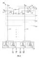
- FIG. 1depicts a block diagram of an exemplary memory circuit with a conventional self-timed access scheme
- FIG. 2(Prior Art) illustrates a timing diagram for a read access operation using the conventional scheme
- FIG. 3depicts a block diagram of an exemplary memory circuit provided in accordance with the teachings of the present invention.
- FIG. 4depicts a block diagram of a portion of the exemplary memory circuit of the present invention wherein the row decoder is provided with a built-in precision shutdown apparatus for reducing power consumption during access operations;
- FIG. 5depicts an exemplary embodiment of the built-in shutdown circuitry of the present invention
- FIG. 6depicts an exemplary core memory cell
- FIG. 7depicts an exemplary reference cell provided in accordance with the teachings of the present invention as part of the built-in shutdown circuitry for low-power access operations;
- FIG. 8illustrates a timing diagram for a read access operation using the built-in shutdown scheme of the present invention.
- FIG. 9illustrates a timing diagram for a write access operation using the built-in shutdown scheme of the present invention.
- FIG. 1depicted therein is a block diagram of an exemplary embodiment of a memory circuit 100 having a conventional self-timed access scheme for effectuating read and write operations.
- the layout of the conventional memory circuit 100includes a plurality of memory cells organized into an array 102 , wherein reference numeral 104 refers to an exemplary core memory cell that can be accessed using the conventional access control scheme set forth below.
- a wordline (WL) 105 and a pair of complementary bitlines, BT 107 and BB 109are associated with the core cell 104 in well known manner.
- a control logic block 106 operable responsive to a clock (CLK) signal 111 and a plurality of address signals 113 , a precharge and sense amplifier (sense amp or SA) circuit block 130 , and a row decoder (XDEC) block 108 having WL driver circuitryare also provided conventionally with respect to the array 102 .
- the conventional memory circuit 100also includes the following components: a reference decoder and driver block 110 operable in conjunction with a reference WL (RWL) block 112 wherein.
- RWL 114is exemplary, a read reference cell block. 116 , a read reference column block 120 having a pair of complementary reference bitlines (RBT 122 and RBB 124 ), a read reference comparator block 128 , a write reference comparator block 118 , and a write reference column block 126 .
- a self-timed clock (STCLK) signal 132is provided from the reference comparator 128 to the control logic 106 to shut off the access cycle in the conventional scheme.
- FIG. 2depicts a timing diagram for a read access operation using the conventional self-timed scheme which illustrates some of the drawbacks and deficiencies associated therewith.
- CLK 111Upon assertion of CLK 111 , as exemplified by a rising edge 202 therein, selected WL 105 is driven HIGH.
- Reference numeral 204refers to the rising edge of WL 105 generated responsive to the CLK signal.
- RWL 114is also driven HIGH, but at a slower rate than the rate of selected WL because of the differences in the WL and RWL driver circuits.
- Reference numeral 205refers to the rising edge in RWL 114 , which is illustrated with a slope that is not as steep as the slope of WL's rising edge 204 . Because the RWL signal starts later than the selected WL and due to the differences in the respective rising edge slopes, there is introduced at the outset a dead time D 1 in the timing loop associated with the read cycle.
- the voltage levels of the reference BT and BB signal paths associated with a reference cellare separated such that a voltage difference 206 (typically a few hundred millivolts) is developed therebetween.
- a voltage difference 206typically a few hundred millivolts
- an access shutdown loopis initiated by a falling edge 208 created in STCLK 132 responsive to the voltage differential 206 between RBT 122 and RBB 124 .
- the selected WL 210is driven LOW (reference-numeral 210 ) responsive to the falling edge 208 of STCLK 132 .
- D 2dead time
- the voltage differential developed on the core cell's complementary bitlines (BT and BB, not shown in this FIG.) due to the data stored thereatis properly sensed by the SA circuitry 130 of the memory circuit 100 .
- RWL 114is driven LOW (reference numeral 212 ) and, responsive thereto, STCLK 132 is driven HIGH (reference numeral 214 ), completing the read cycle.
- FIG. 3shown therein is a block schematic of an exemplary memory circuit 300 provided in accordance with the teachings of the present invention, wherein a self-referenced, built-in precision shutdown circuit apparatus is integrated within a row decoder 308 associated therewith.
- the memory circuit 300includes a plurality of memory cells organized into an array 302 , which may be architected in any known or heretofore unknown manner, e.g., vertical and horizontal banking, centrally-disposed XDEC in the array, et cetera.
- Reference numeral 304refers to an exemplary core memory cell of the array 302 , wherein WL 305 and complementary bitlines, BT 307 and BB 309 , may be conventionally associated therewith.
- the memory circuit 300can be provided with precharge and SA circuitry 320 for effectuating memory operations in normal manner.
- a clock (CLK) signal 316which can be a Bank Select signal or Bank Clock signal in a banked memory implementation, and a plurality of address signals 318 are provided to a control logic block 306 included in the memory circuit 300 .
- the control logic block 306includes control circuitry, described in additional detail hereinbelow, to effectuate the self-referenced shutdown mechanism integrated within the row decoder block 308 .
- the present inventionprovides for an arrangement wherein a WL selected for accessing a core cell itself is utilized for referencing a shutdown sequence.
- a reference cell 310 disposed within XDEC block 308 along the WL selection pathis activatable by a control signal manufactured from the selected WL.
- a pair of complementary reference bitlines, Bitline_Start (BLS) 312 and Bitline_End (BLE) 314associated with the reference memory cell 310 are controlled by reference bitline control circuitry disposed in the control logic block 306 .
- the present invention's self-referenced access shutdown loop arrangement disposed within the row decoder circuitrynot only obviates the need for separate areas required for the conventional self-timed access loop components, but the power consumption associated with access cycle operations is also advantageously reduced by precisely controlling the duration for which a selected WL needs to be driven HIGH.
- the access cycle timeis also improved by eliminating the dead times associated with the conventional self-timed access scheme.
- FIG. 4depicts a block diagram of a portion 400 of the exemplary memory circuit 300 of the present invention wherein the row decoder 308 is provided with a built-in precision shutdown apparatus for reducing power consumption during access operations.
- the memory array 302is depicted as a plurality of columns comprising core cells, wherein reference numerals 412 - 1 through 412 -(N+1) refer to core cells forming one exemplary column associated with I/O 414 and reference numerals 420 - 1 through 420 -(N+1) refer to core cells forming another exemplary column associated with I/O 416 .
- Each column of core cellsis associated with a write driver to effectuate the write access operations.
- reference numerals 410 and 418refer to the two write drivers associated with the two I/O columns 414 and 416 , respectively.
- each column of core cellsis associated with the complementary BT and BB lines in conventional manner.
- a reference column 408comprising a plurality of reference cells, reference numerals 406 - 1 through 406 -(N+1), is disposed within XDEC 308 .
- the pair of BLS 312 and BLE 314 signalsfor controlling the timing of the self-referenced access path in which a selected WL itself acts as a reference WL.
- a BLS/BLE control block 402is operable responsive at least in part to CLK 316 in order to control the voltage levels on BLS 312 and BLE 314 for facilitating a fine-tuned regulation of a selected WL's pulse width pursuant to an access cycle operation.
- each reference cellis operable responsive to a Wordline_Start (WLS) signal that is manufactured from a selected portion of row address signals by way of a decode circuit associated therewith.
- WLSWordline_Start
- a plurality of decode circuits 404 - 1 through 404 -(N+1)are disposed in XDEC 308 , each operating to generate a WLS signal that is provided to the corresponding reference cell.
- a selected portion of row address signals 405are decoded by decode circuitry 404 -N to generate WLS 407 .
- reference cell 406 -NOperating responsive thereto, reference cell 406 -N generates a reference cell data signal, QB 422 , which is buffered through a wordline buffer/generator 424 for driving selected WL 426 HIGH.
- the selected WL 426is looped back via appropriate logic 428 to generate a Wordline_End (WLE) signal 430 that is applied to the reference cell 406 -N.
- WLEWordline_End
- the operation of a reference cell in conjunction with BLS and BLE control signals and WLS/WLE signalsprovides a self-referenced access control scheme that is integrated within the row decoder 308 of the memory circuit.
- FIG. 4shows the reference cell column as part of the row decoder, it may be placed elsewhere in the memory circuit as long as the essential concept of “self-feedback” is implemented with respect to the selected WL for an access operation.
- at least a reference cell columnmay be provided as a column in the array itself, with the WL-based feedback provided separately for purpose of effectuating the self-referenced shutdown mechanism of the present invention.
- the address decode circuitry operable to generate WLS signalscan be treated together as wordline control circuitry 432 for purposes of effectuating self-referenced shutdown for access operations in accordance with the teachings of the present invention.
- this circuitryincludes circuit means to select a particular WL for an access operation and circuit means for deselecting that WL based on a feedback signal derived from the WL itself.
- FIG. 5depicted therein is an exemplary embodiment of the built-in access shutdown circuitry 500 of the present invention, which shows further details of an exemplary reference cell 504 and associated BLS/BLE control circuitry 402 .
- the reference cell 504is a particular exemplary implementation of the reference cells 406 - 1 through 406 -(N+1) depicted in FIG. 4, wherein a cross-coupled latch is operable to support two data nodes, QT and QB, that are internal to it.
- Reference numerals 502 - 1 through 502 - 3refer to three exemplary self-referenced access control circuitry portions, each of which corresponds to a WL of the memory array and includes a reference cell and associated driver/logic combination. Particularly referring to the exemplary reference cell 504 , node QT is coupled to BLS 312 by means of a first access transistor ATR- 1 . Similarly, node QB is coupled to BLE 314 by means of a second access transistor ATR- 2 . In one implementation, these access transistors of the reference cell may be comprised of NMOS devices.
- WLS 407is provided to the gate of access transistor ATR- 1 .
- access transistor ATR- 1is in ON condition and node QT of the reference cell is pulled to the level present on BLS 312 .
- the other data node, i.e., QBwill then be driven to the complementary level, which is propagated through the WL buffer circuitry 424 to appropriately drive the selected WL 426 .
- the buffer circuitry 424may comprise a number of suitably-sized inverters operable to drive the WL line to appropriate logic levels.
- the WL signal 426is looped back via logic circuitry 428 to generate WLE 430 which drives the gate of the second access transistor ATR- 2 of the exemplary reference cell.
- the number and sizes of the devices provided in the logic circuitry 428can be selected with sufficient control such that the timing of the WLE signal can be fine-tuned.
- WLE 430when WLE 430 is driven HIGH, the access transistor ATR- 2 is turned ON and the QB node is pulled to the logic level present on the BLE signal 314 .
- the BLS/BLE control block 402includes various logic circuits necessary to drive the BLS and BLE signals to different levels depending upon the access operation involved.
- a BLS read control block 510 and a BLE read control block 514are operable to control read access operations.
- a BLS write control block 512 and a BLE write control block 516are operable to control write access operations.
- the BLS read control block 510is operable to pull the BLS signal down at least substantially as soon as the CLK signal (or, the Bank Select signal, as the case may be) is asserted in order to initiate the read cycle.
- the BLE read control block 514is operable to pull the BLE signal down by a current that is substantially about N times larger than the accessed core cell's read current. Additionally, the operation of the BLS and BLE read control blocks may be modulated by the use of one or more Read Margin (RM) control signals 506 .
- RMRead Margin
- the BLS write control block 512is operable to pull the BLS signal down by a device that mimics a write driver, but with a weaker drive. After the accessed core cell is flipped, the BLE signal is pulled down by the BLE write control block 516 in order to shut down the WL upon writing (i.e., storing new data). Similar to the read access modulation, the operation of the BLS and BLE write control blocks may be modulated during the write cycle by one or more Write Margin (WM) control signals 507 . Additionally, a Read/Write control (R/W) signal 508 is provided to select whether a read cycle or a write cycle is to follow.
- WMWrite Margin
- R/WRead/Write control
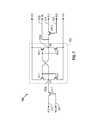
- FIG. 6depicts an exemplary core memory cell 600 coupled to a pair of complementary bitlines, BIT TRUE (BT) and BIT BAR (BB) (reference numerals 604 A and 604 B, respectively), associated with a selected column, which is illustrative of columns 414 and/or 416 shown in FIG. 4 .
- Each of the complementary bitlinesis coupled to appropriate precharge circuitry (not shown in this FIG.) such that it is pulled to a power supply rail or a reference voltage source (typically V DD or any portion thereof) when the precharge circuitry is activated.
- the exemplary memory cell 600is comprised of a cross-coupled CMOS latch 606 .
- a first PMOS transistor MP- 1has the source/drain thereof connected between V DD and a first data node (XT) 602 A, with the gate thereof connected to a second data node (XB) 602 B, the data nodes 602 A and 602 B comprising the two complementary storage nodes in the memory cell 600 .
- a first NMOS transistor MN- 1has the source/drain thereof connected between the data node 602 A and a reference level, e.g., V SS , with the gate thereof connected to the data node 602 B.
- a second PMOS transistor MP- 2has the source/drain thereof connected between V DD and the data node 602 B, with the gate thereof connected to the data node 602 A.
- a second NMOS transistor MN- 2has the source/drain thereof connected between the data node 602 B and V SS reference, and the gate thereof also connected to the data node 602 A.
- a first NMOS access transistor ATM- 1is disposed between BT 604 A and the internal data node 602 A, with the gate thereof coupled to a wordline (e.g., WL 426 ) associated with the memory cell 600 .
- a second NMOS access transistor ATM- 2has the source/drain thereof connected between BB 604 B and the data node 602 B, wherein the gate of the NMOS ATM- 2 is driven by the wordline.
- the cross-coupled inverters of the memory cellform latch 606 , where nodes XT and XB will always hold complementary full swing data values.
- WL 426is held LOW and the precharge circuitry associated with the bitlines is activated so as to equalize the bitline voltage level to a predetermined high voltage. Since the bitlines BT and BB run the entire length of a column of memory cells disposed in the memory array bank, there is a significant amount of capacitance associated with these bitlines.
- the precharge circuitry(not shown) is turned off and the wordline 426 is activated so as to turn on the access transistors ATM- 1 and ATM- 2 . Accordingly, the data node XT 602 A is coupled to BT 604 A and the data node XB 602 B is coupled to BB 604 B.
- transistor MN- 1would be turned ON and transistor MP- 1 would be turned OFF. Thus, transistor MN- 1 would pull BT 604 A LOW, discharging the capacitance on the bitline.
- FIG. 7depicts an exemplary reference cell 700 provided in accordance with the teachings of the present invention as part of the self-referenced, precision built-in shutdown circuitry for low-power access operations, which reference cell is illustrative of reference cells 406 - 1 through 406 -(N+1) shown in FIG. 4 .
- the reference cell 700is comprised of a cross-coupled CMOS latch 706 operable to support two internal data nodes, QT 702 A and QB 702 B.
- Transistors RP- 1 and RN- 1form one inverter and transistors RP- 2 and RN- 2 form the other inverter of the cross-coupled latch 706 .
- QT 702 Ais coupled to BLS 312 via ATR- 1 that is gated by WLS 407
- QB 702 Bis coupled to BLE 314 via ATR- 2 that is gated by WLE 430 .
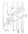
- FIG. 8depicted therein is a timing diagram which illustrates a read access operation using the self-referenced built-in shutdown scheme of the present invention.
- CLK 316Upon assertion of CLK 316 as indicated by a rising edge 802 therein, BLS 312 is pulled LOW by the BLS read control logic.
- Reference numeral 804refers to the falling edge therein.
- WLS(not explicitly shown) and WL 426 are driven HIGH;
- reference numeral 806refers to the rising edge of WL 426 that is generated based on the QB signal provided by the selected reference cell in the row decoder block.
- BLE read control logicoperates to drive BLE 430 LOW at a much faster rate, as illustrated by slope 812 therein, than the development of voltage differential on the BB/BT pair coupled to the accessed core cell.
- Reference numeral 810refers to the shallow slope of the BB/BT pair which traces the voltage differential needed for accurate sensing.
- V ⁇ 808As the voltage BB/BT differential is developed, there is a substantial level on BLE 430 , as indicated by V ⁇ 808 , that triggers a shutdown of WL 426 .
- Reference numeral 814refers to the falling edge created for deselecting the wordline.
- Reference numeral 816refers to the portion of WL being driven HIGH in the prior art memory access schemes, which indicates a wider WL pulse and hence more power consumption in the core. It should be appreciated by one of ordinary skill in the art that by controlling BLE logic, the required differential on the core bitlines can be precisely controlled, whereby WL pulse width may be modulated with accuracy.
- FIG. 9illustrated therein is a timing diagram for a write access operation using the built-in shutdown scheme of the present invention.
- CLK 316(or, an appropriate control signal, e.g., a Bank Select or Bank Clock signal in a multi-bank memory) is asserted (indicated by rising edge 902 ) to start the access operation.
- Voltage levels of the core bitlines(BT and BB lines) are separated by pulling down the appropriate bitline depending upon the data value to be stored.
- the voltage levels of the reference bitlinesi.e., BLE/BLS pair
- BLS 312 LOWillustrated therein is a timing diagram for a write access operation using the built-in shutdown scheme of the present invention.
- Reference numeral 906refers to the shallow slope of the BLS drive.
- the BLS voltage level 907reaches the reference cell's write trip level, data on the internal nodes QT 702 A and QB 702 B of the reference cell is flipped as indicated by reference numeral 908 .
- the voltage level on the pulled BLis substantially near zero and the selected WL 426 is driven HIGH.
- Reference numeral 910refers to the rising edge therein, indicating the active status of WL 426 .
- the core cell data nodes 602 A/ 602 B flip(as indicated by reference numeral 912 ), storing the data value thereat.
- BLE write control logicoperates to pull BLE down (not shown), whereupon WL 426 is deactivated as indicated by its falling edge 916 .
- BLS levelis equalized and, subsequently, the write cycle is terminated.
- the selected WLis driven HIGH only for the time period necessary to flip the core cell, thereby saving power in core bitline discharge (for columns that are not written to).
- the WLis started only when the BT/BB paths in the core are completely separated (i.e., at or substantially near zero), and it is terminated as soon as the reference cell nodes flip back.
- Additional types of memoriesincluding, e.g., register files, content addressable memories (CAMs), and the like, can also advantageously implement the self-referenced built-in shutdown scheme of the present invention.
- the specific components and gatescomprising the sense amp circuitry, precharge circuitry, BLS read/write control logic circuitry, BLE read/write control logic, WL buffer circuitry, etc. should be deemed to be only illustrative rather than limiting, as one of skilled in the art should readily recognize that identical or substantially similar logic functionality may be obtained by various device/gate implementations. Accordingly, all such modifications, substitutions, extensions, additions, combinations, et cetera, should be considered to be within the ambit of the present invention whose scope is limited solely by the claims appended hereinbelow.
Landscapes
- Engineering & Computer Science (AREA)
- Microelectronics & Electronic Packaging (AREA)
- Static Random-Access Memory (AREA)
Abstract
Description
Claims (31)
Priority Applications (1)
| Application Number | Priority Date | Filing Date | Title |
|---|---|---|---|
| US10/223,499US6597629B1 (en) | 2001-11-30 | 2002-08-19 | Built-in precision shutdown apparatus for effectuating self-referenced access timing scheme |
Applications Claiming Priority (2)
| Application Number | Priority Date | Filing Date | Title |
|---|---|---|---|
| US33411101P | 2001-11-30 | 2001-11-30 | |
| US10/223,499US6597629B1 (en) | 2001-11-30 | 2002-08-19 | Built-in precision shutdown apparatus for effectuating self-referenced access timing scheme |
Publications (1)
| Publication Number | Publication Date |
|---|---|
| US6597629B1true US6597629B1 (en) | 2003-07-22 |
Family
ID=26917849
Family Applications (1)
| Application Number | Title | Priority Date | Filing Date |
|---|---|---|---|
| US10/223,499Expired - LifetimeUS6597629B1 (en) | 2001-11-30 | 2002-08-19 | Built-in precision shutdown apparatus for effectuating self-referenced access timing scheme |
Country Status (1)
| Country | Link |
|---|---|
| US (1) | US6597629B1 (en) |
Cited By (41)
| Publication number | Priority date | Publication date | Assignee | Title |
|---|---|---|---|---|
| US20040085800A1 (en)* | 2002-11-05 | 2004-05-06 | Renesas Technology Corp | Semiconductor integrated circuit device |
| US6850446B1 (en) | 2001-12-06 | 2005-02-01 | Virage Logic Corporation | Memory cell sensing with low noise generation |
| US20080301708A1 (en)* | 2007-06-01 | 2008-12-04 | Hamilton Stephen W | Shared storage for multi-threaded ordered queues in an interconnect |
| US20140003172A1 (en)* | 2012-06-29 | 2014-01-02 | Ravindraraj Ramaraju | Memory with word line access control |
| US20140092674A1 (en)* | 2012-09-30 | 2014-04-03 | Shine C. Chung | Circuits and Methods of a Self-Timed High Speed SRAM |
| US8972995B2 (en) | 2010-08-06 | 2015-03-03 | Sonics, Inc. | Apparatus and methods to concurrently perform per-thread as well as per-tag memory access scheduling within a thread and across two or more threads |
| US9007804B2 (en) | 2012-02-06 | 2015-04-14 | Shine C. Chung | Circuit and system of protective mechanisms for programmable resistive memories |
| US9070437B2 (en) | 2010-08-20 | 2015-06-30 | Shine C. Chung | Circuit and system of using junction diode as program selector for one-time programmable devices with heat sink |
| US9076513B2 (en) | 2010-11-03 | 2015-07-07 | Shine C. Chung | Low-pin-count non-volatile memory interface with soft programming capability |
| US9076526B2 (en) | 2012-09-10 | 2015-07-07 | Shine C. Chung | OTP memories functioning as an MTP memory |
| US9136261B2 (en) | 2011-11-15 | 2015-09-15 | Shine C. Chung | Structures and techniques for using mesh-structure diodes for electro-static discharge (ESD) protection |
| US9224496B2 (en) | 2010-08-11 | 2015-12-29 | Shine C. Chung | Circuit and system of aggregated area anti-fuse in CMOS processes |
| US9236141B2 (en) | 2010-08-20 | 2016-01-12 | Shine C. Chung | Circuit and system of using junction diode of MOS as program selector for programmable resistive devices |
| US9251893B2 (en) | 2010-08-20 | 2016-02-02 | Shine C. Chung | Multiple-bit programmable resistive memory using diode as program selector |
| US9281038B2 (en) | 2010-11-03 | 2016-03-08 | Shine C. Chung | Low-pin-count non-volatile memory interface |
| US9293220B2 (en) | 2010-11-03 | 2016-03-22 | Shine C. Chung | Low-pin-count non-volatile memory interface for 3D IC |
| US9305973B2 (en) | 2010-08-20 | 2016-04-05 | Shine C. Chung | One-time programmable memories using polysilicon diodes as program selectors |
| US9324447B2 (en) | 2012-11-20 | 2016-04-26 | Shine C. Chung | Circuit and system for concurrently programming multiple bits of OTP memory devices |
| CN105577150A (en)* | 2014-10-17 | 2016-05-11 | 円星科技股份有限公司 | Pulse Width Regulator |
| US9378808B2 (en)* | 2014-10-17 | 2016-06-28 | M31 Technology Corporation | Pulse width modulation device |
| US9412473B2 (en) | 2014-06-16 | 2016-08-09 | Shine C. Chung | System and method of a novel redundancy scheme for OTP |
| US9460807B2 (en) | 2010-08-20 | 2016-10-04 | Shine C. Chung | One-time programmable memory devices using FinFET technology |
| US9496033B2 (en) | 2010-08-20 | 2016-11-15 | Attopsemi Technology Co., Ltd | Method and system of programmable resistive devices with read capability using a low supply voltage |
| US9496265B2 (en) | 2010-12-08 | 2016-11-15 | Attopsemi Technology Co., Ltd | Circuit and system of a high density anti-fuse |
| US9548109B2 (en) | 2011-02-14 | 2017-01-17 | Attopsemi Technology Co., Ltd | Circuit and system of using FinFET for building programmable resistive devices |
| US9672938B2 (en) | 2014-04-22 | 2017-06-06 | Nxp Usa, Inc. | Memory with redundancy |
| US9711237B2 (en) | 2010-08-20 | 2017-07-18 | Attopsemi Technology Co., Ltd. | Method and structure for reliable electrical fuse programming |
| US9818478B2 (en) | 2012-12-07 | 2017-11-14 | Attopsemi Technology Co., Ltd | Programmable resistive device and memory using diode as selector |
| US9824768B2 (en) | 2015-03-22 | 2017-11-21 | Attopsemi Technology Co., Ltd | Integrated OTP memory for providing MTP memory |
| CN105577150B (en)* | 2014-10-17 | 2018-08-31 | 円星科技股份有限公司 | Pulse wave width adjusting device |
| US10192615B2 (en) | 2011-02-14 | 2019-01-29 | Attopsemi Technology Co., Ltd | One-time programmable devices having a semiconductor fin structure with a divided active region |
| US10229746B2 (en) | 2010-08-20 | 2019-03-12 | Attopsemi Technology Co., Ltd | OTP memory with high data security |
| US10249379B2 (en) | 2010-08-20 | 2019-04-02 | Attopsemi Technology Co., Ltd | One-time programmable devices having program selector for electrical fuses with extended area |
| US10535413B2 (en) | 2017-04-14 | 2020-01-14 | Attopsemi Technology Co., Ltd | Low power read operation for programmable resistive memories |
| US10586832B2 (en) | 2011-02-14 | 2020-03-10 | Attopsemi Technology Co., Ltd | One-time programmable devices using gate-all-around structures |
| US10726914B2 (en) | 2017-04-14 | 2020-07-28 | Attopsemi Technology Co. Ltd | Programmable resistive memories with low power read operation and novel sensing scheme |
| US10770160B2 (en) | 2017-11-30 | 2020-09-08 | Attopsemi Technology Co., Ltd | Programmable resistive memory formed by bit slices from a standard cell library |
| US10916317B2 (en) | 2010-08-20 | 2021-02-09 | Attopsemi Technology Co., Ltd | Programmable resistance memory on thin film transistor technology |
| US10923204B2 (en) | 2010-08-20 | 2021-02-16 | Attopsemi Technology Co., Ltd | Fully testible OTP memory |
| US11062786B2 (en) | 2017-04-14 | 2021-07-13 | Attopsemi Technology Co., Ltd | One-time programmable memories with low power read operation and novel sensing scheme |
| US11615859B2 (en) | 2017-04-14 | 2023-03-28 | Attopsemi Technology Co., Ltd | One-time programmable memories with ultra-low power read operation and novel sensing scheme |
Citations (2)
| Publication number | Priority date | Publication date | Assignee | Title |
|---|---|---|---|---|
| US4739497A (en)* | 1981-05-29 | 1988-04-19 | Hitachi, Ltd. | Semiconductor memory |
| US5668766A (en)* | 1996-05-16 | 1997-09-16 | Intel Corporation | Method and apparatus for increasing memory read access speed using double-sensing |
- 2002
- 2002-08-19USUS10/223,499patent/US6597629B1/ennot_activeExpired - Lifetime
Patent Citations (2)
| Publication number | Priority date | Publication date | Assignee | Title |
|---|---|---|---|---|
| US4739497A (en)* | 1981-05-29 | 1988-04-19 | Hitachi, Ltd. | Semiconductor memory |
| US5668766A (en)* | 1996-05-16 | 1997-09-16 | Intel Corporation | Method and apparatus for increasing memory read access speed using double-sensing |
Cited By (58)
| Publication number | Priority date | Publication date | Assignee | Title |
|---|---|---|---|---|
| US6850446B1 (en) | 2001-12-06 | 2005-02-01 | Virage Logic Corporation | Memory cell sensing with low noise generation |
| US7184346B1 (en) | 2001-12-06 | 2007-02-27 | Virage Logic Corporation | Memory cell sensing with low noise generation |
| US6870756B2 (en)* | 2002-11-05 | 2005-03-22 | Renesas Technology Corporation | Semiconductor integrated circuit device |
| US20040085800A1 (en)* | 2002-11-05 | 2004-05-06 | Renesas Technology Corp | Semiconductor integrated circuit device |
| US20080301708A1 (en)* | 2007-06-01 | 2008-12-04 | Hamilton Stephen W | Shared storage for multi-threaded ordered queues in an interconnect |
| US20100115196A1 (en)* | 2007-06-01 | 2010-05-06 | Sonics, Inc. | Shared storage for multi-threaded ordered queues in an interconnect |
| US7814243B2 (en)* | 2007-06-01 | 2010-10-12 | Sonics, Inc. | Shared storage for multi-threaded ordered queues in an interconnect |
| US8166214B2 (en) | 2007-06-01 | 2012-04-24 | Sonics, Inc. | Shared storage for multi-threaded ordered queues in an interconnect |
| US8972995B2 (en) | 2010-08-06 | 2015-03-03 | Sonics, Inc. | Apparatus and methods to concurrently perform per-thread as well as per-tag memory access scheduling within a thread and across two or more threads |
| US9224496B2 (en) | 2010-08-11 | 2015-12-29 | Shine C. Chung | Circuit and system of aggregated area anti-fuse in CMOS processes |
| US10229746B2 (en) | 2010-08-20 | 2019-03-12 | Attopsemi Technology Co., Ltd | OTP memory with high data security |
| US9385162B2 (en) | 2010-08-20 | 2016-07-05 | Shine C. Chung | Programmably reversible resistive device cells using CMOS logic processes |
| US9070437B2 (en) | 2010-08-20 | 2015-06-30 | Shine C. Chung | Circuit and system of using junction diode as program selector for one-time programmable devices with heat sink |
| US9754679B2 (en) | 2010-08-20 | 2017-09-05 | Attopsemi Technology Co., Ltd | One-time programmable memory devices using FinFET technology |
| US9496033B2 (en) | 2010-08-20 | 2016-11-15 | Attopsemi Technology Co., Ltd | Method and system of programmable resistive devices with read capability using a low supply voltage |
| US10923204B2 (en) | 2010-08-20 | 2021-02-16 | Attopsemi Technology Co., Ltd | Fully testible OTP memory |
| US10249379B2 (en) | 2010-08-20 | 2019-04-02 | Attopsemi Technology Co., Ltd | One-time programmable devices having program selector for electrical fuses with extended area |
| US9478306B2 (en) | 2010-08-20 | 2016-10-25 | Attopsemi Technology Co., Ltd. | Circuit and system of using junction diode as program selector for one-time programmable devices with heat sink |
| US9711237B2 (en) | 2010-08-20 | 2017-07-18 | Attopsemi Technology Co., Ltd. | Method and structure for reliable electrical fuse programming |
| US9236141B2 (en) | 2010-08-20 | 2016-01-12 | Shine C. Chung | Circuit and system of using junction diode of MOS as program selector for programmable resistive devices |
| US9251893B2 (en) | 2010-08-20 | 2016-02-02 | Shine C. Chung | Multiple-bit programmable resistive memory using diode as program selector |
| US9460807B2 (en) | 2010-08-20 | 2016-10-04 | Shine C. Chung | One-time programmable memory devices using FinFET technology |
| US9767915B2 (en) | 2010-08-20 | 2017-09-19 | Attopsemi Technology Co., Ltd | One-time programmable device with integrated heat sink |
| US9305973B2 (en) | 2010-08-20 | 2016-04-05 | Shine C. Chung | One-time programmable memories using polysilicon diodes as program selectors |
| US10916317B2 (en) | 2010-08-20 | 2021-02-09 | Attopsemi Technology Co., Ltd | Programmable resistance memory on thin film transistor technology |
| US10127992B2 (en) | 2010-08-20 | 2018-11-13 | Attopsemi Technology Co., Ltd. | Method and structure for reliable electrical fuse programming |
| US9349773B2 (en) | 2010-08-20 | 2016-05-24 | Shine C. Chung | Memory devices using a plurality of diodes as program selectors for memory cells |
| US9343176B2 (en) | 2010-11-03 | 2016-05-17 | Shine C. Chung | Low-pin-count non-volatile memory interface with soft programming capability |
| US9293220B2 (en) | 2010-11-03 | 2016-03-22 | Shine C. Chung | Low-pin-count non-volatile memory interface for 3D IC |
| US9281038B2 (en) | 2010-11-03 | 2016-03-08 | Shine C. Chung | Low-pin-count non-volatile memory interface |
| US9076513B2 (en) | 2010-11-03 | 2015-07-07 | Shine C. Chung | Low-pin-count non-volatile memory interface with soft programming capability |
| US9496265B2 (en) | 2010-12-08 | 2016-11-15 | Attopsemi Technology Co., Ltd | Circuit and system of a high density anti-fuse |
| US9881970B2 (en) | 2011-02-14 | 2018-01-30 | Attopsemi Technology Co. LTD. | Programmable resistive devices using Finfet structures for selectors |
| US10192615B2 (en) | 2011-02-14 | 2019-01-29 | Attopsemi Technology Co., Ltd | One-time programmable devices having a semiconductor fin structure with a divided active region |
| US11011577B2 (en) | 2011-02-14 | 2021-05-18 | Attopsemi Technology Co., Ltd | One-time programmable memory using gate-all-around structures |
| US10586832B2 (en) | 2011-02-14 | 2020-03-10 | Attopsemi Technology Co., Ltd | One-time programmable devices using gate-all-around structures |
| US9548109B2 (en) | 2011-02-14 | 2017-01-17 | Attopsemi Technology Co., Ltd | Circuit and system of using FinFET for building programmable resistive devices |
| US9136261B2 (en) | 2011-11-15 | 2015-09-15 | Shine C. Chung | Structures and techniques for using mesh-structure diodes for electro-static discharge (ESD) protection |
| US9007804B2 (en) | 2012-02-06 | 2015-04-14 | Shine C. Chung | Circuit and system of protective mechanisms for programmable resistive memories |
| US20140003172A1 (en)* | 2012-06-29 | 2014-01-02 | Ravindraraj Ramaraju | Memory with word line access control |
| US9224439B2 (en)* | 2012-06-29 | 2015-12-29 | Freescale Semiconductor, Inc. | Memory with word line access control |
| US9076526B2 (en) | 2012-09-10 | 2015-07-07 | Shine C. Chung | OTP memories functioning as an MTP memory |
| US20140092674A1 (en)* | 2012-09-30 | 2014-04-03 | Shine C. Chung | Circuits and Methods of a Self-Timed High Speed SRAM |
| US9183897B2 (en)* | 2012-09-30 | 2015-11-10 | Shine C. Chung | Circuits and methods of a self-timed high speed SRAM |
| US9324447B2 (en) | 2012-11-20 | 2016-04-26 | Shine C. Chung | Circuit and system for concurrently programming multiple bits of OTP memory devices |
| US9818478B2 (en) | 2012-12-07 | 2017-11-14 | Attopsemi Technology Co., Ltd | Programmable resistive device and memory using diode as selector |
| US10586593B2 (en) | 2012-12-07 | 2020-03-10 | Attopsemi Technology Co., Ltd | Programmable resistive device and memory using diode as selector |
| US9672938B2 (en) | 2014-04-22 | 2017-06-06 | Nxp Usa, Inc. | Memory with redundancy |
| US9412473B2 (en) | 2014-06-16 | 2016-08-09 | Shine C. Chung | System and method of a novel redundancy scheme for OTP |
| CN105577150B (en)* | 2014-10-17 | 2018-08-31 | 円星科技股份有限公司 | Pulse wave width adjusting device |
| CN105577150A (en)* | 2014-10-17 | 2016-05-11 | 円星科技股份有限公司 | Pulse Width Regulator |
| US9378808B2 (en)* | 2014-10-17 | 2016-06-28 | M31 Technology Corporation | Pulse width modulation device |
| US9824768B2 (en) | 2015-03-22 | 2017-11-21 | Attopsemi Technology Co., Ltd | Integrated OTP memory for providing MTP memory |
| US10535413B2 (en) | 2017-04-14 | 2020-01-14 | Attopsemi Technology Co., Ltd | Low power read operation for programmable resistive memories |
| US10726914B2 (en) | 2017-04-14 | 2020-07-28 | Attopsemi Technology Co. Ltd | Programmable resistive memories with low power read operation and novel sensing scheme |
| US11062786B2 (en) | 2017-04-14 | 2021-07-13 | Attopsemi Technology Co., Ltd | One-time programmable memories with low power read operation and novel sensing scheme |
| US11615859B2 (en) | 2017-04-14 | 2023-03-28 | Attopsemi Technology Co., Ltd | One-time programmable memories with ultra-low power read operation and novel sensing scheme |
| US10770160B2 (en) | 2017-11-30 | 2020-09-08 | Attopsemi Technology Co., Ltd | Programmable resistive memory formed by bit slices from a standard cell library |
Similar Documents
| Publication | Publication Date | Title |
|---|---|---|
| US6597629B1 (en) | Built-in precision shutdown apparatus for effectuating self-referenced access timing scheme | |
| US9183897B2 (en) | Circuits and methods of a self-timed high speed SRAM | |
| JP4439167B2 (en) | Semiconductor memory device | |
| US7881147B2 (en) | Clock and control signal generation for high performance memory devices | |
| US8300491B2 (en) | Multiple bitcells tracking scheme for semiconductor memories | |
| CN106328194B (en) | For improving the circuit and method of the boosting rectifier control of SRAM write operation | |
| US8730750B1 (en) | Memory device with control circuitry for generating a reset signal in read and write modes of operation | |
| US7301819B2 (en) | ROM with a partitioned source line architecture | |
| US8295099B1 (en) | Dual port memory with write assist | |
| KR102065531B1 (en) | A memory device and method of performing access operations within such a memory device | |
| CN101937706A (en) | Assisting write operations to data storage cells | |
| US7394682B2 (en) | Bit line dummy core-cell and method for producing a bit line dummy core-cell | |
| KR20140113357A (en) | A memory device and method of controlling leakage current within such a memory device | |
| US10283191B1 (en) | Method and circuit for adaptive read-write operation in self-timed memory | |
| JP2007193943A (en) | Static random access memory | |
| US9384790B2 (en) | Memory device with separately controlled sense amplifiers | |
| US6473356B1 (en) | Low power read circuitry for a memory circuit based on charge redistribution between bitlines and sense amplifier | |
| US5724294A (en) | Self-tracking sense amplifier strobing circuit and method | |
| US6249471B1 (en) | Fast full signal differential output path circuit for high-speed memory | |
| US7116585B2 (en) | Memory systems and methods | |
| US8854902B2 (en) | Write self timing circuitry for self-timed memory | |
| US6356503B1 (en) | Reduced latency row selection circuit and method | |
| US6711092B1 (en) | Semiconductor memory with multiple timing loops | |
| US6816401B2 (en) | Static random access memory (SRAM) without precharge circuitry | |
| JP3814033B2 (en) | Column selection signal control circuit |
Legal Events
| Date | Code | Title | Description |
|---|---|---|---|
| AS | Assignment | Owner name:VIRAGE LOGIC CORP., CALIFORNIA Free format text:ASSIGNMENT OF ASSIGNORS INTEREST;ASSIGNORS:RASZKA, JAROSLAV;PANDEY, ROHIT;REEL/FRAME:013218/0467;SIGNING DATES FROM 20020812 TO 20020816 | |
| STCF | Information on status: patent grant | Free format text:PATENTED CASE | |
| CC | Certificate of correction | ||
| FPAY | Fee payment | Year of fee payment:4 | |
| AS | Assignment | Owner name:SYNOPSYS, INC., CALIFORNIA Free format text:ASSIGNMENT OF ASSIGNORS INTEREST;ASSIGNORS:VIRAGE LOGIC CORPORATION;VL C.V.;ARC CORES LIMITED;AND OTHERS;REEL/FRAME:025105/0907 Effective date:20100902 | |
| FEPP | Fee payment procedure | Free format text:PAYER NUMBER DE-ASSIGNED (ORIGINAL EVENT CODE: RMPN); ENTITY STATUS OF PATENT OWNER: LARGE ENTITY Free format text:PAYOR NUMBER ASSIGNED (ORIGINAL EVENT CODE: ASPN); ENTITY STATUS OF PATENT OWNER: LARGE ENTITY Free format text:PAT HOLDER NO LONGER CLAIMS SMALL ENTITY STATUS, ENTITY STATUS SET TO UNDISCOUNTED (ORIGINAL EVENT CODE: STOL); ENTITY STATUS OF PATENT OWNER: LARGE ENTITY | |
| REMI | Maintenance fee reminder mailed | ||
| FPAY | Fee payment | Year of fee payment:8 | |
| SULP | Surcharge for late payment | Year of fee payment:7 | |
| FPAY | Fee payment | Year of fee payment:12 |