US6596655B1 - Plasma processes for depositing low dielectric constant films - Google Patents
Plasma processes for depositing low dielectric constant filmsDownload PDFInfo
- Publication number
- US6596655B1 US6596655B1US09/957,681US95768101AUS6596655B1US 6596655 B1US6596655 B1US 6596655B1US 95768101 AUS95768101 AUS 95768101AUS 6596655 B1US6596655 B1US 6596655B1
- Authority
- US
- United States
- Prior art keywords
- sih
- dielectric constant
- layer
- oxidizing gas
- compound
- Prior art date
- Legal status (The legal status is an assumption and is not a legal conclusion. Google has not performed a legal analysis and makes no representation as to the accuracy of the status listed.)
- Expired - Lifetime
Links
- WDGIHDJBOKWZIU-UHFFFAOYSA-NC.C.CC[SiH2]CChemical compoundC.C.CC[SiH2]CWDGIHDJBOKWZIU-UHFFFAOYSA-N0.000description1
- MZRIHOJIAPELPB-RQCPZROWSA-NC.C.CO/C=[SiH]/CChemical compoundC.C.CO/C=[SiH]/CMZRIHOJIAPELPB-RQCPZROWSA-N0.000description1
- WPJGZRAZOJNQNM-UHFFFAOYSA-NC.C.CO[SiH2]C[SiH2]CChemical compoundC.C.CO[SiH2]C[SiH2]CWPJGZRAZOJNQNM-UHFFFAOYSA-N0.000description1
- UGFNTZSIMUZFKH-UHFFFAOYSA-NC.CC(C)(C(C)(C)[Si](C)(C)C)[Si](C)(C)CChemical compoundC.CC(C)(C(C)(C)[Si](C)(C)C)[Si](C)(C)CUGFNTZSIMUZFKH-UHFFFAOYSA-N0.000description1
- QJENQTJIFMXWJJ-UHFFFAOYSA-NC.CC[SiH2]OChemical compoundC.CC[SiH2]OQJENQTJIFMXWJJ-UHFFFAOYSA-N0.000description1
- FTNDRPXGOYBXEP-UHFFFAOYSA-NC.C[SiH2]O[SiH2]CChemical compoundC.C[SiH2]O[SiH2]CFTNDRPXGOYBXEP-UHFFFAOYSA-N0.000description1
- UGHUZKZDBHMQGK-UHFFFAOYSA-NC.C[SiH2]O[SiH2]C(C)CChemical compoundC.C[SiH2]O[SiH2]C(C)CUGHUZKZDBHMQGK-UHFFFAOYSA-N0.000description1
- DLYSBWGVIYFJND-UHFFFAOYSA-NC.C[Si](C)(C)C[Si](C)(C)CChemical compoundC.C[Si](C)(C)C[Si](C)(C)CDLYSBWGVIYFJND-UHFFFAOYSA-N0.000description1
- DXPIUZJBQADKPY-UHFFFAOYSA-NCC(C)([Si](C)(C)C)[Si](C)(C)CChemical compoundCC(C)([Si](C)(C)C)[Si](C)(C)CDXPIUZJBQADKPY-UHFFFAOYSA-N0.000description1
- QCIWZIYBBNEPKB-UHFFFAOYSA-N[H][Si](C)(C)C(C)(C)CChemical compound[H][Si](C)(C)C(C)(C)CQCIWZIYBBNEPKB-UHFFFAOYSA-N0.000description1
Images


Classifications
- H—ELECTRICITY
- H01—ELECTRIC ELEMENTS
- H01L—SEMICONDUCTOR DEVICES NOT COVERED BY CLASS H10
- H01L21/00—Processes or apparatus adapted for the manufacture or treatment of semiconductor or solid state devices or of parts thereof
- H01L21/70—Manufacture or treatment of devices consisting of a plurality of solid state components formed in or on a common substrate or of parts thereof; Manufacture of integrated circuit devices or of parts thereof
- H01L21/71—Manufacture of specific parts of devices defined in group H01L21/70
- H01L21/768—Applying interconnections to be used for carrying current between separate components within a device comprising conductors and dielectrics
- H01L21/76801—Applying interconnections to be used for carrying current between separate components within a device comprising conductors and dielectrics characterised by the formation and the after-treatment of the dielectrics, e.g. smoothing
- H01L21/76835—Combinations of two or more different dielectric layers having a low dielectric constant
- C—CHEMISTRY; METALLURGY
- C23—COATING METALLIC MATERIAL; COATING MATERIAL WITH METALLIC MATERIAL; CHEMICAL SURFACE TREATMENT; DIFFUSION TREATMENT OF METALLIC MATERIAL; COATING BY VACUUM EVAPORATION, BY SPUTTERING, BY ION IMPLANTATION OR BY CHEMICAL VAPOUR DEPOSITION, IN GENERAL; INHIBITING CORROSION OF METALLIC MATERIAL OR INCRUSTATION IN GENERAL
- C23C—COATING METALLIC MATERIAL; COATING MATERIAL WITH METALLIC MATERIAL; SURFACE TREATMENT OF METALLIC MATERIAL BY DIFFUSION INTO THE SURFACE, BY CHEMICAL CONVERSION OR SUBSTITUTION; COATING BY VACUUM EVAPORATION, BY SPUTTERING, BY ION IMPLANTATION OR BY CHEMICAL VAPOUR DEPOSITION, IN GENERAL
- C23C16/00—Chemical coating by decomposition of gaseous compounds, without leaving reaction products of surface material in the coating, i.e. chemical vapour deposition [CVD] processes
- C23C16/22—Chemical coating by decomposition of gaseous compounds, without leaving reaction products of surface material in the coating, i.e. chemical vapour deposition [CVD] processes characterised by the deposition of inorganic material, other than metallic material
- C23C16/30—Deposition of compounds, mixtures or solid solutions, e.g. borides, carbides, nitrides
- C23C16/40—Oxides
- C23C16/401—Oxides containing silicon
- H—ELECTRICITY
- H01—ELECTRIC ELEMENTS
- H01L—SEMICONDUCTOR DEVICES NOT COVERED BY CLASS H10
- H01L21/00—Processes or apparatus adapted for the manufacture or treatment of semiconductor or solid state devices or of parts thereof
- H01L21/02—Manufacture or treatment of semiconductor devices or of parts thereof
- H01L21/02104—Forming layers
- H01L21/02107—Forming insulating materials on a substrate
- H01L21/02109—Forming insulating materials on a substrate characterised by the type of layer, e.g. type of material, porous/non-porous, pre-cursors, mixtures or laminates
- H01L21/02205—Forming insulating materials on a substrate characterised by the type of layer, e.g. type of material, porous/non-porous, pre-cursors, mixtures or laminates the layer being characterised by the precursor material for deposition
- H01L21/02208—Forming insulating materials on a substrate characterised by the type of layer, e.g. type of material, porous/non-porous, pre-cursors, mixtures or laminates the layer being characterised by the precursor material for deposition the precursor containing a compound comprising Si
- H—ELECTRICITY
- H01—ELECTRIC ELEMENTS
- H01L—SEMICONDUCTOR DEVICES NOT COVERED BY CLASS H10
- H01L21/00—Processes or apparatus adapted for the manufacture or treatment of semiconductor or solid state devices or of parts thereof
- H01L21/02—Manufacture or treatment of semiconductor devices or of parts thereof
- H01L21/02104—Forming layers
- H01L21/02107—Forming insulating materials on a substrate
- H01L21/02225—Forming insulating materials on a substrate characterised by the process for the formation of the insulating layer
- H01L21/0226—Forming insulating materials on a substrate characterised by the process for the formation of the insulating layer formation by a deposition process
- H01L21/02263—Forming insulating materials on a substrate characterised by the process for the formation of the insulating layer formation by a deposition process deposition from the gas or vapour phase
- H01L21/02271—Forming insulating materials on a substrate characterised by the process for the formation of the insulating layer formation by a deposition process deposition from the gas or vapour phase deposition by decomposition or reaction of gaseous or vapour phase compounds, i.e. chemical vapour deposition
- H01L21/0228—Forming insulating materials on a substrate characterised by the process for the formation of the insulating layer formation by a deposition process deposition from the gas or vapour phase deposition by decomposition or reaction of gaseous or vapour phase compounds, i.e. chemical vapour deposition deposition by cyclic CVD, e.g. ALD, ALE, pulsed CVD
- H—ELECTRICITY
- H01—ELECTRIC ELEMENTS
- H01L—SEMICONDUCTOR DEVICES NOT COVERED BY CLASS H10
- H01L21/00—Processes or apparatus adapted for the manufacture or treatment of semiconductor or solid state devices or of parts thereof
- H01L21/02—Manufacture or treatment of semiconductor devices or of parts thereof
- H01L21/02104—Forming layers
- H01L21/02107—Forming insulating materials on a substrate
- H01L21/02296—Forming insulating materials on a substrate characterised by the treatment performed before or after the formation of the layer
- H01L21/02299—Forming insulating materials on a substrate characterised by the treatment performed before or after the formation of the layer pre-treatment
- H01L21/02304—Forming insulating materials on a substrate characterised by the treatment performed before or after the formation of the layer pre-treatment formation of intermediate layers, e.g. buffer layers, layers to improve adhesion, lattice match or diffusion barriers
- H—ELECTRICITY
- H01—ELECTRIC ELEMENTS
- H01L—SEMICONDUCTOR DEVICES NOT COVERED BY CLASS H10
- H01L21/00—Processes or apparatus adapted for the manufacture or treatment of semiconductor or solid state devices or of parts thereof
- H01L21/02—Manufacture or treatment of semiconductor devices or of parts thereof
- H01L21/02104—Forming layers
- H01L21/02107—Forming insulating materials on a substrate
- H01L21/02296—Forming insulating materials on a substrate characterised by the treatment performed before or after the formation of the layer
- H01L21/02318—Forming insulating materials on a substrate characterised by the treatment performed before or after the formation of the layer post-treatment
- H01L21/02362—Forming insulating materials on a substrate characterised by the treatment performed before or after the formation of the layer post-treatment formation of intermediate layers, e.g. capping layers or diffusion barriers
- H—ELECTRICITY
- H01—ELECTRIC ELEMENTS
- H01L—SEMICONDUCTOR DEVICES NOT COVERED BY CLASS H10
- H01L21/00—Processes or apparatus adapted for the manufacture or treatment of semiconductor or solid state devices or of parts thereof
- H01L21/70—Manufacture or treatment of devices consisting of a plurality of solid state components formed in or on a common substrate or of parts thereof; Manufacture of integrated circuit devices or of parts thereof
- H01L21/71—Manufacture of specific parts of devices defined in group H01L21/70
- H01L21/768—Applying interconnections to be used for carrying current between separate components within a device comprising conductors and dielectrics
- H01L21/76801—Applying interconnections to be used for carrying current between separate components within a device comprising conductors and dielectrics characterised by the formation and the after-treatment of the dielectrics, e.g. smoothing
- H01L21/76802—Applying interconnections to be used for carrying current between separate components within a device comprising conductors and dielectrics characterised by the formation and the after-treatment of the dielectrics, e.g. smoothing by forming openings in dielectrics
- H01L21/76807—Applying interconnections to be used for carrying current between separate components within a device comprising conductors and dielectrics characterised by the formation and the after-treatment of the dielectrics, e.g. smoothing by forming openings in dielectrics for dual damascene structures
- H01L21/76808—Applying interconnections to be used for carrying current between separate components within a device comprising conductors and dielectrics characterised by the formation and the after-treatment of the dielectrics, e.g. smoothing by forming openings in dielectrics for dual damascene structures involving intermediate temporary filling with material
- H—ELECTRICITY
- H01—ELECTRIC ELEMENTS
- H01L—SEMICONDUCTOR DEVICES NOT COVERED BY CLASS H10
- H01L21/00—Processes or apparatus adapted for the manufacture or treatment of semiconductor or solid state devices or of parts thereof
- H01L21/70—Manufacture or treatment of devices consisting of a plurality of solid state components formed in or on a common substrate or of parts thereof; Manufacture of integrated circuit devices or of parts thereof
- H01L21/71—Manufacture of specific parts of devices defined in group H01L21/70
- H01L21/768—Applying interconnections to be used for carrying current between separate components within a device comprising conductors and dielectrics
- H01L21/76801—Applying interconnections to be used for carrying current between separate components within a device comprising conductors and dielectrics characterised by the formation and the after-treatment of the dielectrics, e.g. smoothing
- H01L21/76802—Applying interconnections to be used for carrying current between separate components within a device comprising conductors and dielectrics characterised by the formation and the after-treatment of the dielectrics, e.g. smoothing by forming openings in dielectrics
- H01L21/76807—Applying interconnections to be used for carrying current between separate components within a device comprising conductors and dielectrics characterised by the formation and the after-treatment of the dielectrics, e.g. smoothing by forming openings in dielectrics for dual damascene structures
- H01L21/7681—Applying interconnections to be used for carrying current between separate components within a device comprising conductors and dielectrics characterised by the formation and the after-treatment of the dielectrics, e.g. smoothing by forming openings in dielectrics for dual damascene structures involving one or more buried masks
- H—ELECTRICITY
- H01—ELECTRIC ELEMENTS
- H01L—SEMICONDUCTOR DEVICES NOT COVERED BY CLASS H10
- H01L21/00—Processes or apparatus adapted for the manufacture or treatment of semiconductor or solid state devices or of parts thereof
- H01L21/70—Manufacture or treatment of devices consisting of a plurality of solid state components formed in or on a common substrate or of parts thereof; Manufacture of integrated circuit devices or of parts thereof
- H01L21/71—Manufacture of specific parts of devices defined in group H01L21/70
- H01L21/768—Applying interconnections to be used for carrying current between separate components within a device comprising conductors and dielectrics
- H01L21/76801—Applying interconnections to be used for carrying current between separate components within a device comprising conductors and dielectrics characterised by the formation and the after-treatment of the dielectrics, e.g. smoothing
- H01L21/76829—Applying interconnections to be used for carrying current between separate components within a device comprising conductors and dielectrics characterised by the formation and the after-treatment of the dielectrics, e.g. smoothing characterised by the formation of thin functional dielectric layers, e.g. dielectric etch-stop, barrier, capping or liner layers
- H01L21/76832—Multiple layers
- H—ELECTRICITY
- H01—ELECTRIC ELEMENTS
- H01L—SEMICONDUCTOR DEVICES NOT COVERED BY CLASS H10
- H01L21/00—Processes or apparatus adapted for the manufacture or treatment of semiconductor or solid state devices or of parts thereof
- H01L21/70—Manufacture or treatment of devices consisting of a plurality of solid state components formed in or on a common substrate or of parts thereof; Manufacture of integrated circuit devices or of parts thereof
- H01L21/71—Manufacture of specific parts of devices defined in group H01L21/70
- H01L21/768—Applying interconnections to be used for carrying current between separate components within a device comprising conductors and dielectrics
- H01L21/76801—Applying interconnections to be used for carrying current between separate components within a device comprising conductors and dielectrics characterised by the formation and the after-treatment of the dielectrics, e.g. smoothing
- H01L21/76829—Applying interconnections to be used for carrying current between separate components within a device comprising conductors and dielectrics characterised by the formation and the after-treatment of the dielectrics, e.g. smoothing characterised by the formation of thin functional dielectric layers, e.g. dielectric etch-stop, barrier, capping or liner layers
- H01L21/76834—Applying interconnections to be used for carrying current between separate components within a device comprising conductors and dielectrics characterised by the formation and the after-treatment of the dielectrics, e.g. smoothing characterised by the formation of thin functional dielectric layers, e.g. dielectric etch-stop, barrier, capping or liner layers formation of thin insulating films on the sidewalls or on top of conductors
- H—ELECTRICITY
- H01—ELECTRIC ELEMENTS
- H01L—SEMICONDUCTOR DEVICES NOT COVERED BY CLASS H10
- H01L21/00—Processes or apparatus adapted for the manufacture or treatment of semiconductor or solid state devices or of parts thereof
- H01L21/02—Manufacture or treatment of semiconductor devices or of parts thereof
- H01L21/02104—Forming layers
- H01L21/02107—Forming insulating materials on a substrate
- H01L21/02109—Forming insulating materials on a substrate characterised by the type of layer, e.g. type of material, porous/non-porous, pre-cursors, mixtures or laminates
- H01L21/02112—Forming insulating materials on a substrate characterised by the type of layer, e.g. type of material, porous/non-porous, pre-cursors, mixtures or laminates characterised by the material of the layer
- H01L21/02123—Forming insulating materials on a substrate characterised by the type of layer, e.g. type of material, porous/non-porous, pre-cursors, mixtures or laminates characterised by the material of the layer the material containing silicon
- H01L21/02126—Forming insulating materials on a substrate characterised by the type of layer, e.g. type of material, porous/non-porous, pre-cursors, mixtures or laminates characterised by the material of the layer the material containing silicon the material containing Si, O, and at least one of H, N, C, F, or other non-metal elements, e.g. SiOC, SiOC:H or SiONC
- H—ELECTRICITY
- H01—ELECTRIC ELEMENTS
- H01L—SEMICONDUCTOR DEVICES NOT COVERED BY CLASS H10
- H01L21/00—Processes or apparatus adapted for the manufacture or treatment of semiconductor or solid state devices or of parts thereof
- H01L21/02—Manufacture or treatment of semiconductor devices or of parts thereof
- H01L21/02104—Forming layers
- H01L21/02107—Forming insulating materials on a substrate
- H01L21/02109—Forming insulating materials on a substrate characterised by the type of layer, e.g. type of material, porous/non-porous, pre-cursors, mixtures or laminates
- H01L21/02112—Forming insulating materials on a substrate characterised by the type of layer, e.g. type of material, porous/non-porous, pre-cursors, mixtures or laminates characterised by the material of the layer
- H01L21/02123—Forming insulating materials on a substrate characterised by the type of layer, e.g. type of material, porous/non-porous, pre-cursors, mixtures or laminates characterised by the material of the layer the material containing silicon
- H01L21/02164—Forming insulating materials on a substrate characterised by the type of layer, e.g. type of material, porous/non-porous, pre-cursors, mixtures or laminates characterised by the material of the layer the material containing silicon the material being a silicon oxide, e.g. SiO2
- H—ELECTRICITY
- H01—ELECTRIC ELEMENTS
- H01L—SEMICONDUCTOR DEVICES NOT COVERED BY CLASS H10
- H01L21/00—Processes or apparatus adapted for the manufacture or treatment of semiconductor or solid state devices or of parts thereof
- H01L21/02—Manufacture or treatment of semiconductor devices or of parts thereof
- H01L21/02104—Forming layers
- H01L21/02107—Forming insulating materials on a substrate
- H01L21/02109—Forming insulating materials on a substrate characterised by the type of layer, e.g. type of material, porous/non-porous, pre-cursors, mixtures or laminates
- H01L21/02203—Forming insulating materials on a substrate characterised by the type of layer, e.g. type of material, porous/non-porous, pre-cursors, mixtures or laminates the layer being porous
- H—ELECTRICITY
- H01—ELECTRIC ELEMENTS
- H01L—SEMICONDUCTOR DEVICES NOT COVERED BY CLASS H10
- H01L21/00—Processes or apparatus adapted for the manufacture or treatment of semiconductor or solid state devices or of parts thereof
- H01L21/02—Manufacture or treatment of semiconductor devices or of parts thereof
- H01L21/02104—Forming layers
- H01L21/02107—Forming insulating materials on a substrate
- H01L21/02109—Forming insulating materials on a substrate characterised by the type of layer, e.g. type of material, porous/non-porous, pre-cursors, mixtures or laminates
- H01L21/02205—Forming insulating materials on a substrate characterised by the type of layer, e.g. type of material, porous/non-porous, pre-cursors, mixtures or laminates the layer being characterised by the precursor material for deposition
- H01L21/02208—Forming insulating materials on a substrate characterised by the type of layer, e.g. type of material, porous/non-porous, pre-cursors, mixtures or laminates the layer being characterised by the precursor material for deposition the precursor containing a compound comprising Si
- H01L21/02211—Forming insulating materials on a substrate characterised by the type of layer, e.g. type of material, porous/non-porous, pre-cursors, mixtures or laminates the layer being characterised by the precursor material for deposition the precursor containing a compound comprising Si the compound being a silane, e.g. disilane, methylsilane or chlorosilane
- H—ELECTRICITY
- H01—ELECTRIC ELEMENTS
- H01L—SEMICONDUCTOR DEVICES NOT COVERED BY CLASS H10
- H01L21/00—Processes or apparatus adapted for the manufacture or treatment of semiconductor or solid state devices or of parts thereof
- H01L21/02—Manufacture or treatment of semiconductor devices or of parts thereof
- H01L21/02104—Forming layers
- H01L21/02107—Forming insulating materials on a substrate
- H01L21/02109—Forming insulating materials on a substrate characterised by the type of layer, e.g. type of material, porous/non-porous, pre-cursors, mixtures or laminates
- H01L21/02205—Forming insulating materials on a substrate characterised by the type of layer, e.g. type of material, porous/non-porous, pre-cursors, mixtures or laminates the layer being characterised by the precursor material for deposition
- H01L21/02208—Forming insulating materials on a substrate characterised by the type of layer, e.g. type of material, porous/non-porous, pre-cursors, mixtures or laminates the layer being characterised by the precursor material for deposition the precursor containing a compound comprising Si
- H01L21/02214—Forming insulating materials on a substrate characterised by the type of layer, e.g. type of material, porous/non-porous, pre-cursors, mixtures or laminates the layer being characterised by the precursor material for deposition the precursor containing a compound comprising Si the compound comprising silicon and oxygen
- H01L21/02216—Forming insulating materials on a substrate characterised by the type of layer, e.g. type of material, porous/non-porous, pre-cursors, mixtures or laminates the layer being characterised by the precursor material for deposition the precursor containing a compound comprising Si the compound comprising silicon and oxygen the compound being a molecule comprising at least one silicon-oxygen bond and the compound having hydrogen or an organic group attached to the silicon or oxygen, e.g. a siloxane
- H—ELECTRICITY
- H01—ELECTRIC ELEMENTS
- H01L—SEMICONDUCTOR DEVICES NOT COVERED BY CLASS H10
- H01L21/00—Processes or apparatus adapted for the manufacture or treatment of semiconductor or solid state devices or of parts thereof
- H01L21/02—Manufacture or treatment of semiconductor devices or of parts thereof
- H01L21/02104—Forming layers
- H01L21/02107—Forming insulating materials on a substrate
- H01L21/02225—Forming insulating materials on a substrate characterised by the process for the formation of the insulating layer
- H01L21/0226—Forming insulating materials on a substrate characterised by the process for the formation of the insulating layer formation by a deposition process
- H01L21/02263—Forming insulating materials on a substrate characterised by the process for the formation of the insulating layer formation by a deposition process deposition from the gas or vapour phase
- H01L21/02271—Forming insulating materials on a substrate characterised by the process for the formation of the insulating layer formation by a deposition process deposition from the gas or vapour phase deposition by decomposition or reaction of gaseous or vapour phase compounds, i.e. chemical vapour deposition
- H01L21/02274—Forming insulating materials on a substrate characterised by the process for the formation of the insulating layer formation by a deposition process deposition from the gas or vapour phase deposition by decomposition or reaction of gaseous or vapour phase compounds, i.e. chemical vapour deposition in the presence of a plasma [PECVD]
- H—ELECTRICITY
- H01—ELECTRIC ELEMENTS
- H01L—SEMICONDUCTOR DEVICES NOT COVERED BY CLASS H10
- H01L2221/00—Processes or apparatus adapted for the manufacture or treatment of semiconductor or solid state devices or of parts thereof covered by H01L21/00
- H01L2221/10—Applying interconnections to be used for carrying current between separate components within a device
- H01L2221/1005—Formation and after-treatment of dielectrics
- H01L2221/101—Forming openings in dielectrics
- H01L2221/1015—Forming openings in dielectrics for dual damascene structures
- H01L2221/1031—Dual damascene by forming vias in the via-level dielectric prior to deposition of the trench-level dielectric
- Y—GENERAL TAGGING OF NEW TECHNOLOGICAL DEVELOPMENTS; GENERAL TAGGING OF CROSS-SECTIONAL TECHNOLOGIES SPANNING OVER SEVERAL SECTIONS OF THE IPC; TECHNICAL SUBJECTS COVERED BY FORMER USPC CROSS-REFERENCE ART COLLECTIONS [XRACs] AND DIGESTS
- Y10—TECHNICAL SUBJECTS COVERED BY FORMER USPC
- Y10T—TECHNICAL SUBJECTS COVERED BY FORMER US CLASSIFICATION
- Y10T428/00—Stock material or miscellaneous articles
- Y10T428/24—Structurally defined web or sheet [e.g., overall dimension, etc.]
- Y10T428/24802—Discontinuous or differential coating, impregnation or bond [e.g., artwork, printing, retouched photograph, etc.]
- Y10T428/24926—Discontinuous or differential coating, impregnation or bond [e.g., artwork, printing, retouched photograph, etc.] including ceramic, glass, porcelain or quartz layer
- Y—GENERAL TAGGING OF NEW TECHNOLOGICAL DEVELOPMENTS; GENERAL TAGGING OF CROSS-SECTIONAL TECHNOLOGIES SPANNING OVER SEVERAL SECTIONS OF THE IPC; TECHNICAL SUBJECTS COVERED BY FORMER USPC CROSS-REFERENCE ART COLLECTIONS [XRACs] AND DIGESTS
- Y10—TECHNICAL SUBJECTS COVERED BY FORMER USPC
- Y10T—TECHNICAL SUBJECTS COVERED BY FORMER US CLASSIFICATION
- Y10T428/00—Stock material or miscellaneous articles
- Y10T428/31504—Composite [nonstructural laminate]
- Y10T428/31652—Of asbestos
- Y10T428/31663—As siloxane, silicone or silane
Definitions
- the present inventionrelates to the fabrication of integrated circuits. More particularly, the invention relates to a process and apparatus for depositing dielectric layers on a substrate.
- the liner layer 2is an oxidized silane film that has effective barrier properties when deposited in a manner which provides a dielectric constant of at least 4.5.
- the dielectric constant of the oxidized silane filmcan be decreased to about 4.1 by altering process conditions in a manner that decreases moisture barrier properties of the film.
- Conventional liner layers, such as SiNhave even higher dielectric constants, and the combination of low k dielectric layers with high k dielectric liner layers can provide little or no improvement in the overall stack dielectric constant and capacitive coupling.
- a preferred silicon oxide layeris produced by reaction of nitrous oxide, N 2 O, and a silicon compound containing Si—H bonds, such as methylsilane, CH 3 SiH 3 , dimethylsilane, (CH 3 ) 2 SiH 2 , or 1,1,3,3-tetramethyl-disiloxane, (CH 3 ) 2 —SiH—O—SiH—(CH 3 ) 2 .
- a silicon compound containing Si—H bondssuch as methylsilane, CH 3 SiH 3 , dimethylsilane, (CH 3 ) 2 SiH 2 , or 1,1,3,3-tetramethyl-disiloxane, (CH 3 ) 2 —SiH—O—SiH—(CH 3 ) 2 .
- the silicon oxide layersare cured at low pressure and high temperature to stabilize properties.
- the silicon oxide layersare most preferably produced using separate applications of RF power to the deposition chamber to increase porosity of the deposited layers.
- the use of low levels of RF poweris preferred at chamber pressures less than about 10 Torr.
- Microwave poweris preferably provided to oxidizing gases in a dissociation chamber to control formation of reactive oxidizers without increasing the power level in the deposition chamber.
- the silicon oxide of the present inventionhas further utility in an integrated process for manufacture of reliable dual damascene structures in one deposition chamber to reduced capacitive coupling between interconnect lines.
- a low k dielectric film having high carbon contentgreater than about 20% by atomic weight, is deposited as a via level dielectric layer.
- a low k dielectric film having a low carbon content, less than about 10% by atomic weight,is then deposited on the high carbon layer to form a trench level dielectric layer.
- a dual damascene etchthen forms the trenches in the trench level dielectric layer and stops at the via level dielectric layer. After etching the vias in the via level dielectric layer, the upper surface is then planarized to leave a planar surface on the trench level dielectric layer.
- the inventionfurther provides an intermetal dielectric material (IMD) comprising the silicon oxide which is deposited on a conventional etch stop such as silicon oxide or silicon nitride.
- IMDintermetal dielectric material
- the silicon oxidecan also be deposited as a thin adhesive layer.
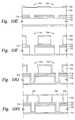
- FIGS. 1A-1Bare schematic diagrams of dielectric layers deposited on a substrate by the processes known in the art
- FIG. 2is a cross-sectional diagram of an exemplary CVD plasma reactor configured for use according to the present invention
- FIG. 4is a flow chart of a process control computer program product used in conjunction with the exemplary CVD plasma reactor of FIG. 2;
- FIG. 5is a flow chart illustrating steps undertaken in depositing liner and cap layers in a gap filling process according to one embodiment of the present invention
- FIG. 9is a cross sectional view showing an adhesive layer comprising the silicon oxide layer of the present invention between a premetal dielectric layer and an intermetal dielectric layer;
- FIGS. 10A-10Hare cross sectional views showing a dual damascene deposition sequence wherein the silicon oxide of the present invention is used to adhere an intermetal dielectric film to a conventional etch stop;
- FIGS. 11A-11Dare cross sectional views showing an integrated dual damascene deposition sequence wherein the silicon oxide of the present invention is used to eliminate a conventional etch stop.
- Carbon which remains in the silicon oxide layercontributes to low dielectric constants and barrier properties.
- the remaining carbonis between about 1% and about 50% by atomic weight, and preferably includes sufficient C—H or C—F bonds to provide hydrophobic properties to the silicon oxide layer resulting in significantly lower dielectric constants and improved moisture barrier properties.
- the silicon oxide layersare produced from silicon compounds that include carbon in organo groups that are not readily removed by oxidation at processing conditions.
- the —C—H bondsare included such as in alkyl or aryl groups, or fluorinated carbon derivatives thereof.
- Suitable organo groupsalso can include alkenyl and cyclohexenyl groups and functional derivatives.
- the organo silicon compoundsinclude:
- the organo silicon compoundsare oxidized during deposition by reaction with oxygen (O 2 ) or oxygen containing compounds such as nitrous oxide (N 2 O), ozone (O 3 ), carbon dioxide (CO 2 ), and water (H 2 O), preferably N 2 O, such that the carbon content of the deposited film is from 1 to 50% by atomic weight, preferably about 5 to 30%.
- the oxidized organo silicon layerhas a dielectric constant of about 3.0 and has excellent barrier properties.
- the oxidized organo silicon layersfurther have high oxide contents in comparison to conventional low k dielectric layers and good adhesion properties.
- organosilane and organosiloxane compoundspreferably include the structures:
- an organosilane or organosiloxane compoundincludes two or more Si atoms
- each Siis separated from another Si by —O—, —C—, or —C—C—, wherein C is included in an organo group, preferably alkyl or alkenyl groups such as —CH 2 —, —CH 2 —CH 2 —, —CH(CH 3 ) —or —C(CH 3 ) 2 —, or fluorinated derivatives thereof.
- the preferred organosilane and organosiloxane compoundsare gases or liquids near room temperature and can be volatilized above about 10 Torr.
- Preferred organosilanes and organosiloxanesinclude:
- the hydrocarbon groups in the organosilanes and organosiloxanemay be partially or fully fluorinated to convert C—H bonds to C—F bonds.
- Many of the preferred organosilane and organosiloxane compoundsare commercially available.
- a combination of two or more of the organosilanes or organosiloxanescan be employed to provide a blend of desired properties such as dielectric constant, oxide content, hydrophobicity, film stress, and plasma etching characteristics.
- organosilane and organosiloxane compoundsare preferably oxidized during deposition by plasma assisted reaction with oxygen which is formed during the deposition process by decomposition of nitrous oxide (N 2 O). Nitrous oxide does not react with the
- the silicon oxide layers of the present inventionare most preferably produced using low levels of constant high frequency RF power or pulsed levels of high frequency RF power.
- Pulsed RF powerpreferably provides 13.56 MHz RF power at about 20 W to about 500 W, most preferably from 20 W to about 250 W, during about 10% to about 30% of the duty cycle.
- Constant RF powerpreferably provides 13.56 MHz RF power at about 10 W to about 200 W, preferably from about 20 W to about 100 W.
- Low power depositionpreferably occurs at a temperature range from about ⁇ 20° C. to about 40° C. At the preferred temperature range, the deposited film is partially polymerized during deposition and polymerization is completed during subsequent curing of the film.
- the system controller 34controls all of the activities of the CVD reactor and a preferred embodiment of the controller 34 includes a hard disk drive, a floppy disk drive, and a card rack.
- the card rackcontains a single board computer (SBC), analog and digital input/output boards, interface boards and stepper motor controller boards.
- SBCsingle board computer
- the system controllerconforms to the Versa Modular Europeans (VME) standard which defines board, card cage, and connector dimensions and types.
- VMEVersa Modular Europeans
- the VME standardalso defines the bus structure having a 16-bit data but and 24-bit address bus.
- the system controller 34operates under the control of a computer program stored on the hard disk drive 38 .
- the computer programdictates the timing, mixture of gases, RF power levels, susceptor position, and other parameters of a particular process.
- the interface between a user and the system controlleris via a CRT monitor 40 and light pen 44 which are depicted in FIG. 3 .
- a second monitor 42is used, the first monitor 40 being mounted in the clean room wall for the operators and the other monitor 42 behind the wall for the service technicians. Both monitors 40 , 42 simultaneously display the same information but only one light pen 44 is enabled.
- the light pen 44detects light emitted by CRT display with a light sensor in the tip of the pen.
- the operatortouches a designated area of the display screen and pushes the button on the pen 44 .
- the touched areachanges its highlighted color, or a new menu or screen is displayed, confirming communication between the light pen and the display screen.
- the process gas control subroutine 460has program code for controlling process gas composition and flow rates.
- the process gas control subroutine 460controls the open/close position of the safety shut-off valves, and also ramps up/down the mass flow controllers to obtain the desired gas flow rate.
- the process gas control subroutine 460is invoked by the chamber manager subroutine 440 , as are all chamber components subroutines, and receives from the chamber manager subroutine process parameters related to the desired gas flow rates.
- a gap fill layeris then deposited 210 on the liner layer by known methods.
- the gap fill layeris preferably self-planarizing, such as spin-on polymers or oxides deposited in liquid form by reaction of methyl silane and hydrogen peroxide.
- a cap layeris then deposited 215 on the gap fill layer, preferably using the same process for depositing the lining layer. The wafer is then removed 220 from the reactor 10 .
- the three-layer gap filling processprovides a PECVD lining layer 300 of the oxidized organosilane or organosiloxane polymer.
- the lining layer 300acts as an isolation layer between a subsequent gap fill layer 302 and the underlying substrate surface 304 and metal lines 306 , 308 , 310 formed on the substrate surface.
- the gap fill layer 302is capped by a PECVD capping layer 312 of the oxidized organosilane or organosiloxane polymer. This process is implemented and controlled using a computer program stored in the memory 38 of a computer controller 34 for a CVD reactor 10 .
- Gap filling layers produced from methylsilaneare typically hydrophilic and have poor moisture barrier properties.
- a gap filling layer produced from methylsilaneWhen deposited on a lining layer produced from methylsilane, a gap filling layer produced from methylsilane, surprisingly is hydrophobic and has good moisture barrier properties.
- the reactor 10optionally resumes deposition of the oxidized ,organosilane or organosiloxane layer of the present invention for deposition of a capping layer 312 .
- the deposited layersare cured in a furnace or another chamber at a temperature from about 100° C. to about 450 EC to drive off remaining solvent or water.
- processing conditionswill vary according to the desired characteristics of the deposited films.
- the damascene structurealternatively includes the oxidized organosilane or organsiloxane as an intermetal dielectric.
- a first dielectric layer 510preferably consisting of the oxidized organosilane or organosiloxane, is deposited on a substrate 512 and then a conventional silicon oxide, silicon nitride, or hydrogenated silicon carbide etch stop 514 is deposited on the first dielectric layer. The etch stop is then patterned to define the openings of the contacts/vias 516 .
- a second dielectric layer 518consisting of the oxidized organosilane or organosiloxane, is then deposited over the patterned etch stop and then patterned to define the interconnect lines 520 .
- a single etch processis then performed to define the interconnects down to the etch stop and to etch the unprotected dielectric exposed by the patterned etch stop to define the contacts/vias.
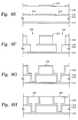
- a preferred dual damascene structure fabricated in accordance with the inventionincludes a lining layer as shown in FIG. 8H, and the method of making the structure is sequentially depicted schematically in FIGS. 8A-8H, which are cross sectional views of a substrate having the steps of the invention formed thereon.
- interconnects and contacts/viasare then etched using reactive: ion etching or other anisotropic etching techniques to define the metallization structure (i.e., the interconnect and contact/via) as shown in FIG. 8 F.
- Any photo resist or other material used to pattern the etch stop 514 or the second dielectric layer 518is removed using an oxygen strip or other suitable process.
- the metallization structureis then formed with a conductive material such as aluminum, copper, tungsten or combinations thereof.
- a conductive materialsuch as aluminum, copper, tungsten or combinations thereof.
- the trendis to use copper to form the smaller features due to the low resistivity of copper (1.7 mW-cm compared to 3.1 mW-cm for aluminum).
- a suitable barrier layer 524such as tantalum nitride is first deposited conformally in the metallization pattern to prevent copper migration into the surrounding silicon and/or dielectric material.
- copper 526is deposited using either chemical vapor deposition, physical vapor deposition, electroplating, or combinations thereof to form the conductive structure.
- the surfaceis planarized using chemical mechanical polishing, as shown in FIG. 8 H.
- a dual damascene structurewhich includes an oxidized organosilane or organosiloxane layer as an adhesive layer between a premetal dielectric layer and an intermetal dielectric layer is shown in FIG. 9 .
- the oxidized organosilane or organosiloxane adhesive layer 612is deposited on a premetal dielectric layer 610 such as a conventional PSG or BPSG layer and then cured.
- An intermetal dielectric layer 614preferably a low k dielectric polymer layer, is then deposited over the adhesive layer 612 .
- a conventional silicon oxide or silicon nitride etch stop 616is then patterned by conventional methods to define vias 620 .
- a second intermetal dielectric layer 622preferably the low k dielectric polymer, is then deposited over the patterned etch stop and then patterned to define the interconnect lines.
- a single etch processis then performed to define the interconnects down to the etch stop and to etch the unprotected dielectric exposed by the patterned etch stop to define the contacts/vias prior to metallization.
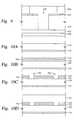
- FIGS. 10A-10Hare cross sectional views of a substrate having the steps of the invention formed thereon.
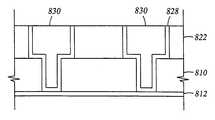
- an initial first intermetal dielectric layer 710such as parylene, FSG, silicon oxide, or the like, is deposited on a substrate 712 to a thickness of about 5,000 to about 10,000 ⁇ , depending on the size of the structure to be fabricated.
- a low k adhesive layer 714which is the oxidized organo silane layer, is then deposited on the first intermetal dielectric layer 710 to a thickness of about 50 to about 200 ⁇ .
- a conventional silicon oxide or silicon nitride etch stop 716is the deposited on the adhesive layer 714 to a thickness of about 50 to about 200 ⁇ .
- a second low k adhesive layer 718which is the oxidized organo silane layer, is then deposited on the etch stop 716 to a thickness of about 50 to about 200 ⁇ .
- the etch stop 716 and adhesive layers 714 , 718are then pattern etched to define the contact/via openings 720 and to expose first intermetal dielectric layer 710 in the areas where the contacts/vias are to be formed as shown in FIG. 10 C.
- the etch stop 716is pattern etched using conventional photolithography and etch processes using fluorine, carbon, and oxygen ions.
- a second intermetal dielectric layer 722is deposited over second adhesive layer 718 to a thickness of about 5,000 to about 10,000 ⁇ as shown in FIG. 10 D.
- the second intermetal dielectric layer 722is then patterned to define interconnect lines 724 , preferably using conventional photolithography processes with a photo resist layer 726 as shown in FIG. 10 E.
- the interconnects and contacts/viasare then etched using reactive ion etching or other anisotropic etching techniques to define the metallization structure (i.e., the interconnect and contact/via) as shown in FIG. 10 F.
- Any photo resist or other material used to pattern the etch stop 716 or the second intermetal dielectric layer 722is removed using an oxygen strip or other suitable process.
- the metallization structureis then formed with a conductive material such as aluminum, copper, tungsten or combinations thereof.
- a conductive materialsuch as aluminum, copper, tungsten or combinations thereof.
- the trendis to use copper to form the smaller features due to the low resistivity of copper (1.7 mW-cm compared to 3.1 mW-cm for aluminum).
- a suitable barrier layer 728such as tantalum nitride is first deposited conformally in the metallization pattern to prevent copper migration into the surrounding silicon and/or dielectric material. Thereafter, copper is deposited using either chemical vapor deposition, physical vapor deposition, electroplating, or combinations thereof to form the conductive structure.
- the surfaceis planarized using chemical mechanical polishing, as shown in FIG. 10 H.
- FIGS. 11A-11Dare cross sectional views of a substrate having the steps of the invention formed thereon.
- the metallization structureis then formed with a conductive material such as aluminum, copper, tungsten or combinations thereof.
- a conductive materialsuch as aluminum, copper, tungsten or combinations thereof.
- the trendis to use copper to form the smaller features due to the low resistivity of copper (1.7 mW-cm compared to 3.1 mW-cm for aluminum).
- a suitable barrier layer 828such as tantalum nitride is first deposited conformally in the metallization pattern to prevent copper migration into the surrounding silicon and/or dielectric material.
- copper 830is deposited as shown in FIG. 11D using either chemical vapor deposition, physical vapor deposition, electroplating, or combinations thereof to form the conductive structure.
- the surfaceis planarized using chemical mechanical polishing or other planarizing methods.
- the following exampledemonstrates deposition of an oxidized organosilane or organosiloxane film having excellent barrier and adhesion properties.
- This examplewas undertaken using a chemical vapor deposition chamber, and in particular, a “CENTURA DxZ” system which includes a solid-state RF matching unit with a two-piece quartz process kit, both fabricated and sold by Applied Materials, Inc., Santa Clara, Calif.
- Dimethylsilane, (CH 3 ) 2 SiH 2at 55 sccm
- the substratewas positioned 600 mil from the gas distribution showerhead and 20 W of high frequency power (13 MHz) was applied to the showerhead for plasma enhanced deposition of an oxidized dimethylsilane layer.
- the oxidized dimethylsilane materialhad a dielectric constant of about 2.5 and was hydrophobic.
- An oxidized 1,3,5-trisilano-2,4,6-trimethylene (cyclic) filmis deposited at a chamber pressure of 3.0 Torr and temperature of 15 EC from reactive gases which flow into the reactor as follows:
- the substrateis positioned 600 mil from the gas distribution showerhead and 50 W of pulsed high frequency power (13 MHz) is applied to the showerhead for plasma enhanced deposition of an oxidized 1,3,5-trisilano-2,4,6-trimethylene layer.
- 1,3-DimethyldisiloxaneCH 3 —SiH 2 —O—SiH 2 —CH 3 , at 30 sccm Nitrous oxide, N 2 O, at 300 sccm Helium, He, at 4000 sccm.
- the substrateis positioned 600 mil from the gas distribution showerhead and 50 W of pulsed high frequency RF power (13 MHz) is applied to the showerhead for plasma enhanced deposition of an oxidized dimethyldisiloxane layer.
- An oxidized 1,3-dimethyldisiloxane filmis deposited at a chamber pressure of 3.0 Torr and temperature of 15 EC from reactive gases which are flowed into the reactor as follows:
- 1,3-DimethyldisiloxaneCH 3 —SiH 2 —O—SiH 2 —CH 3 , at 30 sccm Nitrous oxide, N 2 O, at 300 sccm Helium, He, at 4000 sccm.
- the nitrous oxidePrior to entering the chamber, the nitrous oxide is dissociated in a microwave applicator that provides 2000 W of microwave energy.
- the substrateis positioned 600 mil from the gas distribution showerhead and 50 W of high frequency RF power (13 MHz) is applied to the showerhead in cycles for plasma enhanced deposition of an oxidized dimethyldisiloxane layer. Each cycle provides RF power for 30% of the cycle.
Landscapes
- Engineering & Computer Science (AREA)
- Physics & Mathematics (AREA)
- Condensed Matter Physics & Semiconductors (AREA)
- General Physics & Mathematics (AREA)
- Manufacturing & Machinery (AREA)
- Computer Hardware Design (AREA)
- Microelectronics & Electronic Packaging (AREA)
- Power Engineering (AREA)
- Chemical & Material Sciences (AREA)
- Chemical Kinetics & Catalysis (AREA)
- Inorganic Chemistry (AREA)
- General Chemical & Material Sciences (AREA)
- Materials Engineering (AREA)
- Mechanical Engineering (AREA)
- Metallurgy (AREA)
- Organic Chemistry (AREA)
- Formation Of Insulating Films (AREA)
- Internal Circuitry In Semiconductor Integrated Circuit Devices (AREA)
- Chemical Vapour Deposition (AREA)
Abstract
Description
This is a divisional of application Ser. No. 09/247,381 filed on Feb. 10, 1999, now U.S. Pat. No. 6,348,725, which is a continuation-in-part of U.S. patent application Ser. No. 09/021,788, which was filed on Feb. 11, 1998, now U.S. Pat. No. 6,054,379, a continuation in part of U.S. patent application Ser. No. 09/114,682, which was filed on Jul. 13, 1998, now U.S. Pat. No. 6,072,227, a continuation-in-part of U.S. patent application Ser. No. 09/162,915, which was filed on Sep. 29, 1998, now U.S. Pat. No. 6,287,990, and a continuation-in-part of U.S. patent application Ser. No. 09/185,555, which was filed on Nov. 4, 1998, now Pat. No. 6,303,523.
The present invention relates to the fabrication of integrated circuits. More particularly, the invention relates to a process and apparatus for depositing dielectric layers on a substrate.
One of the primary steps in the fabrication of modern semiconductor devices is the formation of metal and dielectric films on a substrate by chemical reaction of gases. Such deposition processes are referred to as chemical vapor deposition or CVD. Conventional thermal CVD processes supply reactive gases to the substrate surface where heat-induced chemical reactions take place to produce a desired film. The high temperatures at which some thermal CVD processes operate can damage device structures having layers previously formed on the substrate. A preferred method of depositing metal and dielectric films at relatively low temperatures is plasma-enhanced CVD (PECVD) techniques such as described in U.S. Pat. No. 5,362,526, entitled “Plasma-Enhanced CVD Process Using TEOS for Depositing Silicon Oxide”, which is incorporated by reference herein. Plasma-enhanced CVD techniques promote excitation and/or disassociation of the reactant gases by the application of radio frequency (RF) energy to a reaction zone near the substrate surface, thereby creating a plasma of highly reactive species. The high reactivity of the released species reduces the energy required for a chemical reaction to take place, and thus lowers the required temperature for such PECVD processes.
Semiconductor device geometries have dramatically decreased in size since such devices were first introduced several decades ago. Since then, integrated circuits have generally followed the two year/half-size rule (often called Moore's Law), which means that the number of devices that will fit on a chip doubles every two years. Today's fabrication plants are routinely producing devices having 0.35 μm and even 0.18 μm feature sizes, and tomorrow's plants soon will be producing devices having even smaller geometries.
In order to further reduce the size of devices on integrated circuits, it has become necessary to use conductive materials having low resistivity and insulators having low k (dielectric constant<4.0) to reduce the capacitive coupling between adjacent metal lines. Liner/barrier layers have been used between the conductive materials and the insulators to prevent diffusion of byproducts such as moisture onto the conductive material as described in International Publication Number WO 94/01 885. For example, moisture that can be generated during formation of a low k insulator readily diffuses to the surface of the conductive metal and increases the resistivity of the conductive metal surface. A barrier/liner layer formed from conventional silicon oxide or silicon nitride materials can block the diffusion of the byproducts. However, the barrier/liner layers typically have dielectric constants that are significantly greater than 4.0, and the high dielectric constants result in a combined insulator that does not significantly reduce the dielectric constant.
FIG. 1A illustrates a PECVD process for depositing a barrier/liner layer as described in International Publication Number WO 94/01885. The PECVD process deposits a multi-component dielectric layer wherein a silicon dioxide (SiO2)liner layer 2 is first deposited on a patterned metal layer havingmetal lines 3 formed on asubstrate 4. Theliner layer 2 is deposited by a plasma enhanced reaction of silane (SiH4) and nitrous oxide (N2O) at 300° C. A self-planarizing low kdielectric layer 5 is then deposited on theliner layer 2 by reaction of a silane compound and a peroxide compound. The self-planarizinglayer 5 retains moisture that is removed by curing. Theliner layer 2 is an oxidized silane film that has effective barrier properties when deposited in a manner which provides a dielectric constant of at least 4.5. The dielectric constant of the oxidized silane film can be decreased to about 4.1 by altering process conditions in a manner that decreases moisture barrier properties of the film. Conventional liner layers, such as SiN, have even higher dielectric constants, and the combination of low k dielectric layers with high k dielectric liner layers can provide little or no improvement in the overall stack dielectric constant and capacitive coupling.
As shown in Figure 1B, WO 94/01885 further describes an optional SiO2cap layer6 that is deposited on the low kdielectric layer 5 by the reaction of silane and N2O. The cap layer6 is also an oxidized silane film that has good barrier properties when deposited in a manner that provides a dielectric constant of about 4.5. Both theliner layer 2 and the cap layer6 have a dielectric constant greater than 4.5 and the high dielectric constant layers substantially detract from the benefit of the low kdielectric layer 5.
As devices get smaller, liner layers and cap layers having high dielectric constants contribute more to the overall dielectric constant of a multi-component dielectric layer. Furthermore, known low k dielectric materials generally have low oxide content which makes the material inadequate as an etch stop layer during etching of vias and/or interconnects. Silicon nitride has been the etch stop material of choice for making interconnect lines in low k dielectric materials. However, the silicon nitride has a relatively high dielectric constant (dielectric constant of about 7) compared to the surrounding low k dielectric layers. It has also been discovered that the silicon nitride may significantly increase the capacitive coupling between interconnect lines, even when an otherwise low k dielectric material is used as the primary insulator. This may lead to crosstalk and/or resistance-capacitance (RC) delay that degrades the overall performance of the device. Thus, the silicon nitride etch stop layers are typically removed after etching of the underlying dielectric layers.
Ideally, a low k dielectric layer having both good barrier properties for use as a liner layer and sufficient oxide content for use as an etch stop could be identified and deposited in the same chambers as existing low k dielectric materials. Such barrier layers would not increase the overall dielectric constant of the dielectric layers, and such an etch stop layer would not have to be removed after etching the underlying layers.
U.S. Pat. No. 5,554,570 describes barrier layers for use with thermal CVD silicon oxides wherein an organosilane having a C—H group is oxidized instead of silane to increase the density of deposited films and to improve adhesion between the layers. For example, a thermal CVD layer produced from tetraethoxysilane (TEOS) and ozone, may be deposited between PECVD silicon oxide films produced from an organosilicon and N2O or O2.
The barrier layers described in the '570 patent are preferably dense silicon oxide layers having low carbon contents. The dense layers are deposited using 400 W of high frequency RF power although the use of low frequency RF power is asserted to improve film stress. The barrier layers are preferably produced from alkoxysilanes or chlorinated alkylsilanes and N2O to reduce carbon content and increase the density of the layers.
The '570 patent does not identify process conditions for making barrier layers having low dielectric constants or for making etch stop layers having high oxide contents. The '570 patent also does not suggest use of the described layers as a barrier layer adjacent a low k dielectric layer or as an etch stop.
There remains a need for dielectric layers having low dielectric constants, good barrier properties, and high oxide content for use as barrier layers or etch stop layers in sub-micron devices.
The present invention provides a method and apparatus for depositing a silicon oxide layer having a low dielectric constant. The silicon oxide layer is produced by plasma assisted chemical vapor deposition of an organosilane, an organosiloxane, or combinations thereof, using RF or microwave power to generate reactive oxygen atoms. The properties of the silicon oxide layers are readily controlled by process variations, and different layers can be deposited in one deposition chamber as shown for an improved dual damascene process. In addition, the silicon oxide layers can be used as an adhesive layer between different layers, or as an intermetal dielectric layer. A preferred silicon oxide layer is produced by reaction of nitrous oxide, N2O, and a silicon compound containing Si—H bonds, such as methylsilane, CH3SiH3, dimethylsilane, (CH3)2SiH2, or 1,1,3,3-tetramethyl-disiloxane, (CH3)2—SiH—O—SiH—(CH3)2.
The silicon oxide layers are cured at low pressure and high temperature to stabilize properties. The silicon oxide layers are most preferably produced using separate applications of RF power to the deposition chamber to increase porosity of the deposited layers. The use of low levels of RF power is preferred at chamber pressures less than about 10 Torr. Microwave power is preferably provided to oxidizing gases in a dissociation chamber to control formation of reactive oxidizers without increasing the power level in the deposition chamber.
In a preferred embodiment, a silicon oxide layer is deposited on a patterned metal layer by plasma assisted reaction of one or more organosilane and/or organosiloxane compounds that include Si—H bonds.
The silicon oxide of the present invention has further utility in an integrated process for manufacture of reliable dual damascene structures in one deposition chamber to reduced capacitive coupling between interconnect lines. In a preferred embodiment, a low k dielectric film having high carbon content, greater than about 20% by atomic weight, is deposited as a via level dielectric layer. A low k dielectric film having a low carbon content, less than about 10% by atomic weight, is then deposited on the high carbon layer to form a trench level dielectric layer. A dual damascene etch then forms the trenches in the trench level dielectric layer and stops at the via level dielectric layer. After etching the vias in the via level dielectric layer, the upper surface is then planarized to leave a planar surface on the trench level dielectric layer.
The invention further provides an intermetal dielectric material (IMD) comprising the silicon oxide which is deposited on a conventional etch stop such as silicon oxide or silicon nitride. The silicon oxide can also be deposited as a thin adhesive layer.
So that the manner in which the above recited features, advantages and objects of the present invention are attained and can be understood in detail, a more particular description of the invention, briefly summarized above, may be had by reference to the embodiments thereof which are illustrated in the appended drawings.
It is to be noted, however, that the appended drawings illustrate only typical embodiments of this invention and are therefore not to be considered limiting of its scope, for the invention may admit to other equally effective embodiments.
FIGS. 1A-1B (Prior Art) are schematic diagrams of dielectric layers deposited on a substrate by the processes known in the art;
FIG. 2 is a cross-sectional diagram of an exemplary CVD plasma reactor configured for use according to the present invention;
FIG. 3 is a diagram of the system monitor of the CVD plasma reactor of FIG. 2;
FIG. 4 is a flow chart of a process control computer program product used in conjunction with the exemplary CVD plasma reactor of FIG. 2;
FIG. 5 is a flow chart illustrating steps undertaken in depositing liner and cap layers in a gap filling process according to one embodiment of the present invention;
FIGS. 6A-6E is a schematic diagram of the layers deposited on a substrate by the process of FIG. 5;
FIG. 7 is a cross sectional view showing a dual damascene structure comprising the silicon oxide layers of the present invention;
FIGS. 8A-8H are cross sectional views showing one embodiment of a dual damascene deposition sequence of the present invention;
FIG. 9 is a cross sectional view showing an adhesive layer comprising the silicon oxide layer of the present invention between a premetal dielectric layer and an intermetal dielectric layer;
FIGS. 10A-10H are cross sectional views showing a dual damascene deposition sequence wherein the silicon oxide of the present invention is used to adhere an intermetal dielectric film to a conventional etch stop; and
FIGS. 11A-11D are cross sectional views showing an integrated dual damascene deposition sequence wherein the silicon oxide of the present invention is used to eliminate a conventional etch stop.
For a further understanding of the present invention, reference should be made to the ensuing detailed description.
The present invention provides a method and apparatus for depositing a silicon oxide layer having a low dielectric constant, a high oxide content, and sufficient carbon content to provide barrier properties. The silicon oxide layer comprises an oxidized organosilane or organosiloxane and can be used as a lining layer adjacent other dielectric materials, as an etch stop layer adjacent dielectric materials having lower oxide content, as an intermetal dielectric layer, and as an adhesion layer between different materials. The oxidized organosilane material is deposited by plasma assisted oxidation of the organosilane or organosiloxane compounds using from about 10 W to about 200 W of constant RF power, or from about 20 W to about 500 W of pulsed RF power. The silicon oxide layer can also be deposited using frequent breaks, such as changing chambers or providing cooling time, to improve porosity. The RF power is preferably provided at a high frequency such as between 13 MHz and 14 MHz. The RF power is preferably provided in short duration cycles wherein the power is on at the stated levels for cycles less than about 200 Hz and the on cycles total from about 10% to about 30% of the total duty cycle. Intermittent RF power can operate at higher peak power levels and provide the same total power input as constant RF power at a lower power level.
Carbon which remains in the silicon oxide layer contributes to low dielectric constants and barrier properties. The remaining carbon is between about 1% and about 50% by atomic weight, and preferably includes sufficient C—H or C—F bonds to provide hydrophobic properties to the silicon oxide layer resulting in significantly lower dielectric constants and improved moisture barrier properties.
The silicon oxide layers are produced from silicon compounds that include carbon in organo groups that are not readily removed by oxidation at processing conditions. Preferably the —C—H bonds are included such as in alkyl or aryl groups, or fluorinated carbon derivatives thereof. Suitable organo groups also can include alkenyl and cyclohexenyl groups and functional derivatives. The organo silicon compounds include:
| methylsilane, | CH3—SiH3 |
| dimethylsilane, | (CH3)2—SiH2 |
| trimethylsilane, | (CH3)3—SiH |
| disilanomethane, | SiH3—CH2—SiH3 |
| bis(methylsilano)methane, | CH3—SiH2—CH2—SiH2—CH3 |
| 1,2-disilanoethane, | SiH3—CH2—CH2—SiH3 |
| 1,2-bis(methylsilano)ethane, | CH3-SiH2—CH2—CH2—SiH2—CH3 |
| 2,2-disilanopropane, | SiH3—C(CH3)2—SiH3 |
| 1,3,5-trisilano-2,4,6- | —(—SiH2CH2—)3— (cyclic) |
| trimethylene, | |
| 1,3-dimethyldisiloxane, | CH3—SiH2—O—SiH2—CH3 |
| 1,1,3,3-tetramethyldisiloxane, | (CH3)2—SiH—O—SiH—(CH3)2 |
| 1,3-bis(silanomethylene) | (SiH3—CH2—SiH2—)2—O |
| disiloxane, | |
| bis(1-methyldisiloxanyl) | (CH3—SiH2—O—SiH2—)2—CH2 |
| methane, | |
| 2,2-bis(1-methyldisiloxanyl) | (CH3—SiH2—O—SiH2—)2—C(CH3)2 |
| propane, | |
| 2,4,6,8,10-pentamethylcyclo- | —(—SiHCH3—O—)5— (cyclic) |
| pentasiloxane, and | |
| 1,3,5,7-tetrasilano-2,6-dioxy- | —(—SiH2—CH2—SiH2—O—)2— |
| 4,8-dimethylene, | (cyclic) |
| 2,4,6-trisilanetetrahydropyran, | —SiH2—CH2—SiH2—CH2—SiH2—O— |
| (cyclic) | |
| 2,5-disilanetetrahydrofuran, | —SiH2—CH2—CH2—SiH2—O— |
| (cyclic) | |
The organo silicon compounds are oxidized during deposition by reaction with oxygen (O2) or oxygen containing compounds such as nitrous oxide (N2O), ozone (O3), carbon dioxide (CO2), and water (H2O), preferably N2O, such that the carbon content of the deposited film is from 1 to 50% by atomic weight, preferably about 5 to 30%. The oxidized organo silicon layer has a dielectric constant of about 3.0 and has excellent barrier properties. The oxidized organo silicon layers further have high oxide contents in comparison to conventional low k dielectric layers and good adhesion properties.
Oxygen and oxygen containing compounds are preferably dissociated to increase reactivity when necessary to achieve a desired carbon content in the deposited film. RF power can be coupled to the deposition chamber to increase dissociation of the oxidizing compounds. The oxidizing compounds may also be dissociated in a microwave chamber prior to entering the deposition chamber to reduce excessive dissociation of the silicon containing compounds. Deposition of the silicon oxide layer can be continuous or discontinuous. Although deposition preferably occurs in a single deposition chamber, the layer can be deposited sequentially in two or more deposition chambers. Furthermore, RF power can be cycled or pulsed to reduce heating of the substrate and promote greater porosity in the deposited film. During deposition of the silicon oxide layer, the substrate is maintained at a temperature of from about −20° C. to about 400° C., and preferably is maintained at a temperature of approximately −20° C. to 40° C.

wherein each Si is bonded to one or two carbon atoms, and C is included in an organo group, preferably alkyl or alkenyl groups such as —CH3, —CH2—CH3, —CH2—, or —CH2—CH2, or fluorinated carbon derivatives thereof. The carbon atoms in the fluorinated derivatives may be partially or fully fluorinated to replace hydrogen atoms. When an organosilane or organosiloxane compound includes two or more Si atoms, each Si is separated from another Si by —O—, —C—, or —C—C—, wherein C is included in an organo group, preferably alkyl or alkenyl groups such as —CH2—, —CH2—CH2—, —CH(CH3) —or —C(CH3)2—, or fluorinated derivatives thereof.
The preferred organosilane and organosiloxane compounds are gases or liquids near room temperature and can be volatilized above about 10 Torr. Preferred organosilanes and organosiloxanes include:


and fluorinated carbon derivatives thereof, such as:
| trifluoromethylsilane, | CF3—SiH3 |
| 1,2-disilanotetrafluoroethylene | SiH3—CF2—CF2—SiH3 |
| 1,2-bis(trifluoromethylsilano)tetra- | CF3—SiH2—CF2—CF2—SiH2—CF3 |
| fluoroethane, | |
| 2,2-disilanohexafluoropropane, | SiH3—C(CF3)2—SiH3 |
| 1,3-bis(silanodifluoromethylene) | (SiH3—CF2—SiH2—)2—O |
| disiloxane, | |
| bis(1-trifluormethyldisiloxanyl) | (CF3—SiH2—O—SiH2—)2—CF2 |
| difluoromethane, | |
| 2,4,6-trisilanetetrafluoropyran, and | —SiH2—CF2—SiH2—CF2— |
| SiH2—O— (cyclic) | |
| 2,5-disilanetetrafluorofuran. | —SiH2—CF2—CF2—SiH2—O— |
| (cyclic) | |
The hydrocarbon groups in the organosilanes and organosiloxane may be partially or fully fluorinated to convert C—H bonds to C—F bonds. Many of the preferred organosilane and organosiloxane compounds are commercially available. A combination of two or more of the organosilanes or organosiloxanes can be employed to provide a blend of desired properties such as dielectric constant, oxide content, hydrophobicity, film stress, and plasma etching characteristics.
The organosilane and organosiloxane compounds are preferably oxidized during deposition by plasma assisted reaction with oxygen which is formed during the deposition process by decomposition of nitrous oxide (N2O). Nitrous oxide does not react with the
organosilanes or organosiloxanes without plasma assistance, and the oxygen-nitrogen bonds are readily broken at lower energies than the bonds in the organosilanes and organosiloxanes. The oxidized compounds adhere to contacted surfaces such as a patterned layer of a semiconductor substrate to form a deposited film. The deposited films are cured at low pressure and at temperatures from about 100 to about 450° C., preferably above about 400° C. to stabilize the barrier properties of the films. The deposited film has sufficient carbon content to provide barrier properties. The carbon content preferably includes C—H or C—F bonds to provide a hydrophobic film that is an excellent moisture barrier.
The present invention further provides a substrate processing system having a vessel including a reaction zone, a substrate holder for positioning a substrate in the reaction zone, and a vacuum system. The processing system further comprises a gas/liquid distribution system connecting the reaction zone of the vessel to supplies of an organosilane or organosiloxane compound, an oxidizing gas, and an inert gas, and an RF generator coupled to the gas distribution system for generating a plasma in the reaction zone. The processing system further comprises a controller comprising a computer for controlling the vessel, the gas distribution system, and the RF generator, and a memory coupled to the controller, the memory comprising a computer usable medium comprising a computer readable program code for selecting the process steps of depositing a low dielectric constant film with a plasma of an organosilane or organosiloxane compound and an oxidizing gas.
The processing system may further comprise in one embodiment computer readable program code for selecting the process steps, of depositing a liner of the oxidized organo silicon compound, depositing a different dielectric layer, and optionally depositing a capping layer of the oxidized organo silicon compound.
Further description of the invention relates to a specific apparatus for depositing silicon oxide layers of the present invention and to preferred silicon oxide films.
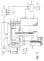
One suitable CVD plasma reactor in which a method of the present invention can be carried out is shown in FIG. 2, which is a vertical, cross-section view of a parallel plate chemicalvapor deposition reactor 10 having ahigh vacuum region 15.Reactor 10 contains agas distribution manifold 11 for dispersing process gases through perforated holes in the manifold to a substrate or wafer (not shown) that rests on a substrate support plate orsusceptor 12 which is raised or lowered by a lift motor14. A liquid injection system (not shown), such as typically used for liquid injection of TEOS, may also be provided for injecting a liquid organosilane and/or organosiloxane compound. The preferred methylsilanes are gases.
Thereactor 10 includes heating of the process gases and substrate, such as by resistive heating coils (not shown) or external lamps (not shown). Referring to FIG. 2,susceptor 12 is mounted on asupport stem 13 so that susceptor12 (and the wafer supported on the upper surface of susceptor12) can be controllably moved between a lower loading/off-loading position and an upper processing position which is closely adjacent tomanifold 11.
When susceptor12 and the wafer are in processing position14, they are surrounded by a aninsulator 17 and process gases exhaust into amanifold 24. During processing, gases inlet tomanifold 11 are uniformly distributed radially across the surface of the wafer. Avacuum pump 32 having a throttle valve controls the exhaust rate of gases from the chamber.
Before reachingmanifold 11, deposition and carrier gases are input throughgas lines 18 into amixing system 19 where they are combined and then sent tomanifold 11. Anoptional microwave applicator 28 can be located on the input gas line for the oxidizing gas to provide additional energy that dissociates only the oxidizing gas. The microwave applicator provides from 0 to 6000 W. Generally, the processgases supply line 18 for each of the process gases also includes (i) safety shut-off valves (not shown) that can be used to automatically or manually shut off the flow of process gas into the chamber, and (ii) mass flow controllers (also not shown) that measure the flow of gas through the gas supply lines. When toxic gases are used in the process, several safety shut-off valves are positioned on each gas supply line in conventional configurations.
The deposition process performed inreactor 10 can be either a thermal process or a plasma enhanced process. In a plasma process, a controlled plasma is typically formed adjacent to the wafer by RF energy applied todistribution manifold 11 from RF power supply25 (withsusceptor 12 grounded). Alternatively, RF power can be provided to thesusceptor 12 or RF power can be provided to different components at different frequencies.RF power supply 25 can supply either single or mixed frequency RF power to enhance the decomposition of reactive species introduced into thehigh vacuum region 15. A mixed frequency RF power supply typically supplies power at a high RF frequency (RFI) of 13.56 MHz to thedistribution manifold 11 and at a low RF frequency (RF2) of 360 KHz to thesusceptor 12. The silicon oxide layers of the present invention are most preferably produced using low levels of constant high frequency RF power or pulsed levels of high frequency RF power. Pulsed RF power preferably provides 13.56 MHz RF power at about 20 W to about 500 W, most preferably from 20 W to about 250 W, during about 10% to about 30% of the duty cycle. Constant RF power preferably provides 13.56 MHz RF power at about 10 W to about 200 W, preferably from about 20 W to about 100 W. Low power deposition preferably occurs at a temperature range from about −20° C. to about 40° C. At the preferred temperature range, the deposited film is partially polymerized during deposition and polymerization is completed during subsequent curing of the film.
When additional dissociation of the oxidizing gas is desired, an optional microwave chamber can be used to input from 0 to 3000 W of microwave power to the oxidizing gas prior to entering the deposition chamber. Separate addition of microwave power would avoid excessive dissociation of the silicon compounds prior to reaction with the oxidizing gas. A gas distribution plate having separate passages for the silicon compound and the oxidizing gas is preferred when microwave power is added to the oxidizing gas.
Typically, any or all of the chamber lining,distribution manifold 11,susceptor 12, and various other reactor hardware is made out of material such as aluminum or anodized aluminum. An example of such a CVD reactor is described in U.S. Pat. No. 5,000,113, entitled AThermal CVD/PECVD Reactor and Use for Thermal Chemical Vapor Deposition of Silicon Dioxide and In-situ Multi-step Planarized Process, issued to Wang et al. And assigned to Applied Materials, Inc., the assignee of the present invention.
The lift motor14 raises and lowerssusceptor 12 between a processing position and a lower, wafer-loading position. The motor, thegas mixing system 19, and theRF power supply 25 are controlled by asystem controller 34 over control lines36. The reactor includes analog assemblies, such as mass flow controllers (MFCs) and standard or pulsed RF generators, that are controlled by thesystem controller 34 which executes system control software stored in amemory 38, which in the; preferred embodiment is a hard disk drive. Motors and optical sensors are used to move and determine the position of movable mechanical assemblies such as the throttle valve of thevacuum pump 32 and motor for positioning thesusceptor 12.
Thesystem controller 34 controls all of the activities of the CVD reactor and a preferred embodiment of thecontroller 34 includes a hard disk drive, a floppy disk drive, and a card rack. The card rack contains a single board computer (SBC), analog and digital input/output boards, interface boards and stepper motor controller boards. The system controller conforms to the Versa Modular Europeans (VME) standard which defines board, card cage, and connector dimensions and types. The VME standard also defines the bus structure having a 16-bit data but and 24-bit address bus.
Thesystem controller 34 operates under the control of a computer program stored on thehard disk drive 38. The computer program dictates the timing, mixture of gases, RF power levels, susceptor position, and other parameters of a particular process. The interface between a user and the system controller is via aCRT monitor 40 andlight pen 44 which are depicted in FIG.3. In the preferred embodiment asecond monitor 42 is used, thefirst monitor 40 being mounted in the clean room wall for the operators and theother monitor 42 behind the wall for the service technicians. Both monitors40,42 simultaneously display the same information but only onelight pen 44 is enabled. Thelight pen 44 detects light emitted by CRT display with a light sensor in the tip of the pen. To select a particular screen or function, the operator touches a designated area of the display screen and pushes the button on thepen 44. The touched area changes its highlighted color, or a new menu or screen is displayed, confirming communication between the light pen and the display screen.
Referring to FIG. 4, the process can be implemented using acomputer program product 410 that runs on, for example, thesystem controller 34. The computer program code can be written in any conventional computer readable programming language such as for example 68000 assembly language, C, C++, or Pascal. Suitable program code is entered into a single file, or multiple files, using a conventional text editor, and stored or embodied in a computer usable medium, such as a memory system of the computer. If the entered code text is in a high level language, the code is compiled, and the resultant compiler code is then linked with an object code of precompiled windows library routines. To execute the linked compiled object code, the system user invokes the object code, causing the computer system to load the code in memory, from which the CPU reads and executes the code to perform the tasks identified in the program.
FIG. 4 shows an illustrative block diagram of the hierarchical control structure of thecomputer program 410. A user enters a process set number and process chamber number into aprocess selector subroutine 420 in response to menus or screens displayed on the CRT monitor40 by using thelight pen 44 interface: The process sets are predetermined sets of process parameters necessary to carry out specified processes, and are identified by predefined set numbers. Theprocess selector subroutine 420 the (i) selects a desired process chamber on a cluster tool such as an Centura® platform (available from Applied Materials, Inc.), and (ii) selects a desired set of process parameters needed to operate the process chamber for performing the desired process. The process parameters for performing a specific process relate to process conditions such as, for example, process gas composition and flow rates, temperature, pressure, plasma conditions such as RF bias power levels and magnetic field power levels, cooling gas pressure, and chamber wall temperature and are provided to the user in the form of a recipe. The parameters specified by the recipe are entered utilizing the light pen/CRT monitor interface.
The signals for monitoring the process are provided by the analog input and digital input boards of system controller and the signals for controlling the process are output on the analog output and digital output boards of thesystem controller 34.
Aprocess sequencer subroutine 430 comprises program code for accepting the identified process chamber and set of process parameters from theprocess selector subroutine 420, and for controlling operation of the various process chambers. Multiple users can enter process set numbers and process chamber numbers, or a user can enter multiple process chamber numbers, so thesequencer subroutine 430 operates to schedule the selected processes in the desired sequence. Preferably thesequencer subroutine 430 includes computer readable program code to perform the steps of (i) monitoring the operation of the process chambers to determine if the chambers are being used, (ii) determining what processes are being carried out in the chambers being used, and (iii) executing the desired process based on availability of a process chamber and type of process to be carried out. Conventional methods of monitoring the process chambers can be used, such as polling. When scheduling which process is to be executed, thesequencer subroutine 430 can be designed to take into consideration the present condition of the process chamber being used in comparison with the desired process conditions for a selected process, or the “age” of each particular user entered request, or any other relevant factor a system programmer desires to include for determining the scheduling priorities.
Once thesequencer subroutine 430 determines which process chamber and process set combination is going to be executed next, thesequencer subroutine 430 causes execution of the process set by passing the particular process set parameters to achamber manager subroutine 440 which controls multiple processing tasks in aprocess chamber 10 according to the process set determined by thesequencer'subroutine 430. For example, thechamber manager subroutine 440 comprises program code for controlling CVD process operations in theprocess chamber 10. Thechamber manager subroutine 440 also controls execution of various chamber component subroutines which control operation of the chamber component necessary to carry out the selected process set. Examples of chamber component subroutines aresusceptor control subroutine 450, processgas control subroutine 460,pressure control subroutine 470,heater control subroutine 480, andplasma control subroutine 490. Those having ordinary skill in the art would readily recognize that other chamber control subroutines can be included depending on what processes are desired to be performed in thereactor 10.
In operation, thechamber manager subroutine 440 selectively schedules or calls the process component subroutines in accordance with the particular process set being executed. Thechamber manager subroutine 440 schedules the process component subroutines similarly to how thesequencer subroutine 430 schedules whichprocess chamber 10 and process set is to be executed next. Typically, thechamber manager subroutine 440 includes steps of monitoring the various chamber components, determining which components needs to be operated based on the process parameters for the process set to be executed, and causing execution of a chamber component subroutine responsive to the monitoring and determining steps.
Operation of particular chamber component subroutines will now be described with reference to FIG.4. The susceptorcontrol positioning subroutine 450 comprises program code for controlling chamber components that are used to load the substrate onto thesusceptor 12, and optionally to lift the substrate to a desired height in thereactor 10 to control the spacing between the substrate and thegas distribution manifold 11. When a substrate is loaded into thereactor 10, thesusceptor 12 is lowered to receive the substrate, and thereafter, thesusceptor 12 is raised to the desired height; in the chamber, to maintain the substrate at a first distance or spacing from thegas distribution manifold 11 during the CVD process. In operation, thesusceptor control subroutine 450 controls movement of thesusceptor 12 in response to process set parameters that are transferred from thechamber manager subroutine 440.
The processgas control subroutine 460 has program code for controlling process gas composition and flow rates. The processgas control subroutine 460 controls the open/close position of the safety shut-off valves, and also ramps up/down the mass flow controllers to obtain the desired gas flow rate. The processgas control subroutine 460 is invoked by thechamber manager subroutine 440, as are all chamber components subroutines, and receives from the chamber manager subroutine process parameters related to the desired gas flow rates. Typically, the processgas control subroutine 460 operates by opening the gas supply lines, and repeatedly (i) reading the necessary mass flow controllers, (ii) comparing the readings to the desired flow rates received from thechamber manager subroutine 440, and (iii) adjusting the flow rates of the gas supply; lines as necessary. Furthermore, the processgas control subroutine 460 includes steps for Monitoring the gas flow rates for unsafe rates, and activating the safety shut-off valves when an unsafe condition is detected.
In some processes, an inert gas such as helium or argon is flowed into thereactor 10 to stabilize the pressure in the chamber before reactive process gases are introduced into the chamber. For these processes, the processgas control subroutine 460 is programmed to include steps for flowing the inert gas into thechamber 10 for an amount of time necessary to stabilize the pressure in the chamber, and then the steps described above would be carried out. Additionally, when a process gas is to be vaporized from a liquid precursor, for example 1,3,5-trisilano-2,4,6-trimethylene (1,3,5-trisilanacyclo-hexane), the processgas control subroutine 460 would be written to include steps for bubbling a delivery gas such as helium through the liquid precursor in a bubbler assembly. For this type of process, the processgas control subroutine 460 regulates the flow of the delivery gas, the pressure in the bubbler, and the bubbler temperature in order to obtain the desired process gas flow rates. As discussed above, the desired process gas flow rates are transferred to the processgas control subroutine 460 as process parameters. Furthermore, the processgas control subroutine 460 includes steps for obtaining the necessary delivery gas flow rate, bubbler pressure, and bubbler temperature for the desired process gas flow rate by accessing a stored table containing the necessary values for a given process gas flow rate. Once the necessary values are obtained, the delivery gas flow rate, bubbler pressure and bubbler temperature are monitored, compared to the necessary values and adjusted accordingly.
Thepressure control subroutine 470 comprises program code for controlling the pressure in thereactor 10 by regulating the size of the opening of the throttle valve in theexhaust pump 32. The size of the opening of the throttle valve is set to control the chamber pressure to the desired level in relation to the total process gas flow, size of the process chamber, and pumping set point pressure for theexhaust pump 32. When thepressure control subroutine 470 is invoked, the desired, or target pressure level is received as a parameter from thechamber manager subroutine 440. Thepressure control subroutine 470 operates to measure the pressure in thereactor 10 by reading one or more conventional pressure manometers connected to the chamber, compare the measure value(s) to the target pressure, obtain PID (proportional, integral, and differential) values from a stored pressure table corresponding to the target pressure, and adjust the throttle valve according to the PID values obtained from the pressure table. Alternatively, thepressure control subroutine 470 can be written to open or close the throttle valve to a particular opening size to regulate thereactor 10 to the desired pressure.
Theheater control subroutine 480 comprises program code for controlling the temperature of the heat modules or radiated heat that is used to heat thesusceptor 12. Theheater control subroutine 480 is also invoked by thechamber manager subroutine 440 and receives a target, or set point, temperature parameter. Theheater control subroutine 480 measures the temperature by measuring voltage output of a thermocouple located in asusceptor 12, compares the measured temperature to the set point temperature, and increases or decreases current applied to the heat module to obtain the set point temperature. The temperature is obtained from the measured; voltage by looking up the corresponding temperature in a stored conversion table, or by calculating the temperature using a fourth order polynomial. Theheater control subroutine 480 gradually controls a ramp up/down of current applied to the heat module. The gradual ramp up/down increases the life and reliability of the heat module. Additionally, a built-in-fail-safe mode can be included to detect process safety compliance, and can shut down operation of the heat module if thereactor 10 is not properly set up.
Theplasma control subroutine 490 comprises program code for setting the RF bias voltage power level applied to the process electrodes in thereactor 10, and optionally, to set the level of the magnetic field generated in the reactor. Similar to the previously described chamber component subroutines, theplasma control subroutine 490 is invoked by thechamber manager subroutine 440.
The above CVD system description is; mainly for illustrative purposes, and other plasma CVD equipment such as electrode cyclotron resonance (ECR) plasma CVD devices, induction-coupled RF high density plasma CVD devices, or the like may be employed. Additionally, variations of the above described system such as variations in susceptor design, heater design, location of RF power connections and others are possible. For example, the wafer could be supported and heated by a resistively heated susceptor. The pretreatment and method for forming a pretreated layer of the pre sent invention is not limited to any specific apparatus or to any specific plasma excitation method.
The oxidized organosilane or organosiloxane layer of the present invention can be used in a three-layer gap filling process as shown in FIG. 5 using the PECVD chamber of FIG.2. Referring to FIG. 5, a wafer is positioned200 in thereactor 10 and an oxidized organosilane layer having a low dielectric constant is deposited205 by a PECVD process from a plasma comprising an organosilane compound and/or a organosiloxane compound. Thedeposition step 205 can include a capacitively coupled plasma or both an inductively and a capacitively coupled plasma in theprocess chamber 15 according to methods known in the art. An inert gas such as helium is commonly used in the PECVD deposition to assist in plasma generation. A gap fill layer is then deposited210 on the liner layer by known methods. The gap fill layer is preferably self-planarizing, such as spin-on polymers or oxides deposited in liquid form by reaction of methyl silane and hydrogen peroxide. A cap layer is then deposited215 on the gap fill layer, preferably using the same process for depositing the lining layer. The wafer is then removed220 from thereactor 10.
Referring to FIGS. 6A-6E, the three-layer gap filling process provides aPECVD lining layer 300 of the oxidized organosilane or organosiloxane polymer. Thelining layer 300 acts as an isolation layer between a subsequentgap fill layer 302 and theunderlying substrate surface 304 andmetal lines gap fill layer 302 is capped by aPECVD capping layer 312 of the oxidized organosilane or organosiloxane polymer. This process is implemented and controlled using a computer program stored in thememory 38 of acomputer controller 34 for aCVD reactor 10.
Referring to FIG. 6A, thePECVD lining layer 300 is deposited in thereactor 10 by introducing an oxidizing gas such as N2O, an organosilane or organosiloxane compound such as CH3SiH3or (CH3)2SiH2, and a carrier gas such as helium. The substrate is maintained at a temperature of from about −20° C. to about 400° C., and preferably is maintained at a temperature of approximately −20° C. to 40° C. throughout the deposition of the PECVD lining layer. ThePECVD lining layer 300 is deposited with a process gas that includes a mixture of the organosilane and/or organosiloxane compound at a flow rate of about 5 sccm to about 500 sccm and the oxidizing gas at a flow rate of about 5 sccm to about 2000 sccm. The process gases are carried by an inert gas such He, Ar, Ne, or a relatively inert gas such as nitrogen, which are typically not incorporated into the film, at a flow rate of from about 0.2 to about 20 lpm. The process gases react at a pressure from about 0.2 to about 20 Torr, preferably less than 10 Torr, to form a conformal silicon oxide layer on thesubstrate surface 304 andmetal lines
For an 8″ single wafer chamber, the high frequency RF source of approximately 13.56 MHz is preferably connected to a gas distribution system and driven at about 10 to about 500 W while a low frequency RF source of about 350 KHz to 1 MHz is optionally connected to a susceptor and driven at about 0 to about 100 W. In a preferred embodiment, the high frequency RF source is driven at about 20 W to about 250 W of pulsed RF power, and the low frequency RF source is driven at about 0 to ab out 50 W of pulsed RF power at a duty cycle from 10% to 30%. The pulsed RF power is preferably cycled in short intervals, most, preferably having a frequency less than about 200 Hz. When the high frequency RF power is constant, the power level preferably ranges from about 20 W to about 100 W.
The oxidized organosilane or organosiloxane layer is then cured at a pressure less than about 10 Torr a temperature from about 100° C. to about 450° C. Optionally, curing could be conducted after deposition of additional dielectric layers.
The above process conditions result in the deposition of a PECVD lining layer300 (at about 2000 Å per minute) with improved barrier characteristics for the subsequent deposition of thegap filling layer 302 shown in FIG.6B. The lining layer obtained from methylsilane has sufficient C—H bonds to be hydrophobic, and is an excellent moisture barrier. Deposition of a hydrophobic lining layer has a surprising and unexpected result of converting subsequent hydrophilic layers to hydrophobic layers.
The process gases for thegap filling layer 302 are preferably SiH4, CH3SiH3, or (CH3)2SiH2and 50 wt% of hydrogen peroxide (H2O2) which is vaporized and mixed with an inert carrier gas, such as helium. However, the gap filling layer can be any dielectric layer which has an acceptable dielectric constant. Alternative silicon containing compounds can be used if byproducts are vapors at deposition conditions. Preferred alternative compounds incorporate oxysilano or silano groups, such as:
trimethylsilane,
disilanomethane,
bis(methylsilano)methane,
1,2-disilanoethane,
2,2-disilanopropane,
1,3,5-trisilano-2,4,6-trimethylene (cyclic),
1,3-bis(silanomethylene)siloxane,
bis(1-methyldisiloxanyl)methane,
2,4,6,8-tetramethylcyclotetrasiloxane, or
1,2-disilanotetrafluoroethane.
The process gas flows range from 0-2000 sccm for He, 10-200 sccm for CH3SiH3, and 0.1 to 3 g/min. for H2O2. The preferred gas flows range from 100-500 sccm for He, 20-100 sccn for CH3SiH3, and 0.1 to 1 g/min. for H2O2. These flow rates are given for a chamber having a volume of approximately 5.5 to 6.5 liters. Preferably,reactor 10 is maintained at a pressure of about 0.2 to about 5 torr during deposition of thegap filling layer 302. Thegap filling layer 302 may be partially cured as shown in FIG. 6C to remove solvents such as water prior to deposition of acap layer 312 as shown in FIG.6D. Curing is done in thereactor 10 by pumping under an inert gas atmosphere under 10 Torr.
Gap filling layers produced from methylsilane are typically hydrophilic and have poor moisture barrier properties. When deposited on a lining layer produced from methylsilane, a gap filling layer produced from methylsilane, surprisingly is hydrophobic and has good moisture barrier properties.
Referring to FIG. 6D, after deposition of thegap filling layer 302, thereactor 10 optionally resumes deposition of the oxidized ,organosilane or organosiloxane layer of the present invention for deposition of acapping layer 312. Referring to FIG. 6E, after deposition of the capping layer, if any, the deposited layers are cured in a furnace or another chamber at a temperature from about 100° C. to about 450 EC to drive off remaining solvent or water. Of course, processing conditions will vary according to the desired characteristics of the deposited films.
A dual damascene structure which includes an oxidized organosilane or organosiloxane layers as an etch stop or as an intermetal dielectric layer is shown in FIG.7. When the oxidized organosilane or organosiloxane is used as an etch stop, a firstdielectric layer 510 is deposited on asubstrate 512 and then the oxidized organosilane or organosiloxane etch stop514 is deposited on the first dielectric layer and cured. The etch stop is then pattern etched to define the openings of the contacts/vias 516. Asecond dielectric layer 518 is then deposited over the patterned etch stop and then pattern etched by conventional methods to define the interconnect lines520. A single etch process is then performed to define the interconnects down to the etch stop and to etch the unprotected dielectric exposed by the patterned etch stop to define the contacts/vias.
Referring again to FIG. 7, the damascene structure alternatively includes the oxidized organosilane or organsiloxane as an intermetal dielectric. Afirst dielectric layer 510, preferably consisting of the oxidized organosilane or organosiloxane, is deposited on asubstrate 512 and then a conventional silicon oxide, silicon nitride, or hydrogenated siliconcarbide etch stop 514 is deposited on the first dielectric layer. The etch stop is then patterned to define the openings of the contacts/vias 516. Asecond dielectric layer 518, consisting of the oxidized organosilane or organosiloxane, is then deposited over the patterned etch stop and then patterned to define the interconnect lines520. A single etch process is then performed to define the interconnects down to the etch stop and to etch the unprotected dielectric exposed by the patterned etch stop to define the contacts/vias.
A preferred dual damascene structure fabricated in accordance with the invention includes a lining layer as shown in FIG. 8H, and the method of making the structure is sequentially depicted schematically in FIGS. 8A-8H, which are cross sectional views of a substrate having the steps of the invention formed thereon.
As shown in FIG. 8A, an initial firstdielectric layer 510, such as parylene, FSG, silicon oxide, or the like, is deposited on thesubstrate 512 to a thickness of about 5,000 to about 10,000 D, depending on the size of the structure to be fabricated. As shown in FIG. 8B, the lowk etch stop 514, which is the oxidized organosilane or organosiloxane layer, is then deposited on the first dielectric layer to a thickness of about 200 to about 1000 D using low levels of RF power. The lowk etch stop 514 is, then pattern etched to define the contact/viaopenings 516 and to expose firstdielectric layer 510 in the areas where the contacts/vias are to be formed as shown in FIG.8C. Preferably, lowk etch stop 514 is pattern etched using conventional photolithography and etch processes using fluorine, carbon, and oxygen ions. After lowk etch stop 514 has been etched to pattern the contacts/vias and the photo resist has been removed, asecond dielectric layer 518 is deposited over etch stop514 to a thickness of about 5,000 to about 10,000 D as shown in FIG. 8D. Asecond dielectric layer 518 is then patterned to defineinterconnect lines 520, preferably using conventional photolithography processes with a photo resistlayer 522 as shown in FIG.8E. The interconnects and contacts/vias are then etched using reactive: ion etching or other anisotropic etching techniques to define the metallization structure (i.e., the interconnect and contact/via) as shown in FIG.8F. Any photo resist or other material used to pattern the etch stop514 or thesecond dielectric layer 518 is removed using an oxygen strip or other suitable process.
The metallization structure is then formed with a conductive material such as aluminum, copper, tungsten or combinations thereof. Presently, the trend is to use copper to form the smaller features due to the low resistivity of copper (1.7 mW-cm compared to 3.1 mW-cm for aluminum). Preferably, as shown in FIG. 8G, asuitable barrier layer 524 such as tantalum nitride is first deposited conformally in the metallization pattern to prevent copper migration into the surrounding silicon and/or dielectric material. Thereafter,copper 526 is deposited using either chemical vapor deposition, physical vapor deposition, electroplating, or combinations thereof to form the conductive structure. Once the structure has been filled with copper or other metal, the surface is planarized using chemical mechanical polishing, as shown in FIG.8H.
A dual damascene structure which includes an oxidized organosilane or organosiloxane layer as an adhesive layer between a premetal dielectric layer and an intermetal dielectric layer is shown in FIG.9. The oxidized organosilane or organosiloxaneadhesive layer 612 is deposited on apremetal dielectric layer 610 such as a conventional PSG or BPSG layer and then cured. An intermetaldielectric layer 614, preferably a low k dielectric polymer layer, is then deposited over theadhesive layer 612. A conventional silicon oxide or siliconnitride etch stop 616 is then patterned by conventional methods to definevias 620. A secondintermetal dielectric layer 622, preferably the low k dielectric polymer, is then deposited over the patterned etch stop and then patterned to define the interconnect lines. A single etch process is then performed to define the interconnects down to the etch stop and to etch the unprotected dielectric exposed by the patterned etch stop to define the contacts/vias prior to metallization.
A preferred dual damascene structure comprising an adhesive layer in accordance with the invention is shown in Fig. 10H, and the method of making the structure is sequentially depicted schematically in FIGS. 10A-10H, which are cross sectional views of a substrate having the steps of the invention formed thereon.
As shown in FIG. 10A, an initial firstintermetal dielectric layer 710, such as parylene, FSG, silicon oxide, or the like, is deposited on asubstrate 712 to a thickness of about 5,000 to about 10,000 Å, depending on the size of the structure to be fabricated. As shown in FIG.10B, a lowk adhesive layer 714, which is the oxidized organo silane layer, is then deposited on the firstintermetal dielectric layer 710 to a thickness of about 50 to about 200 Å. A conventional silicon oxide or siliconnitride etch stop 716 is the deposited on theadhesive layer 714 to a thickness of about 50 to about 200 Å. A second lowk adhesive layer 718, which is the oxidized organo silane layer, is then deposited on the etch stop716 to a thickness of about 50 to about 200 Å. Theetch stop 716 andadhesive layers openings 720 and to expose first intermetaldielectric layer 710 in the areas where the contacts/vias are to be formed as shown in FIG.10C. Preferably, theetch stop 716 is pattern etched using conventional photolithography and etch processes using fluorine, carbon, and oxygen ions. After theetch stop 716 andadhesive layers intermetal dielectric layer 722 is deposited over secondadhesive layer 718 to a thickness of about 5,000 to about 10,000 Å as shown in FIG.10D. The secondintermetal dielectric layer 722 is then patterned to defineinterconnect lines 724, preferably using conventional photolithography processes with a photo resistlayer 726 as shown in FIG.10E. The interconnects and contacts/vias are then etched using reactive ion etching or other anisotropic etching techniques to define the metallization structure (i.e., the interconnect and contact/via) as shown in FIG.10F. Any photo resist or other material used to pattern the etch stop716 or the secondintermetal dielectric layer 722 is removed using an oxygen strip or other suitable process.
The metallization structure is then formed with a conductive material such as aluminum, copper, tungsten or combinations thereof. Presently, the trend is to use copper to form the smaller features due to the low resistivity of copper (1.7 mW-cm compared to 3.1 mW-cm for aluminum). Preferably, as shown in FIG. 10G, asuitable barrier layer 728 such as tantalum nitride is first deposited conformally in the metallization pattern to prevent copper migration into the surrounding silicon and/or dielectric material. Thereafter, copper is deposited using either chemical vapor deposition, physical vapor deposition, electroplating, or combinations thereof to form the conductive structure. Once the structure has been filled with copper or other metal, the surface is planarized using chemical mechanical polishing, as shown in FIG.10H.
Another preferred dual damascene structure comprises silicon oxide layers having different dielectric constants to resist crosstalk between layers, and is deposited as shown in FIGS. 11A-11D, which are cross sectional views of a substrate having the steps of the invention formed thereon.
As shown in FIG. 11A, a vialevel dielectric layer 810, having a carbon content greater than 20% by atomic weight, is deposited on asubstrate 812 to a thickness of about 5,000 to about 10,000 Å, depending on the size of the structure to be fabricated. The via level dielectric layer is preferably deposited by reacting N2O and trimethylsilane at an RF power level of 500 W with a duty cycle of 10%. As shown in FIG. 11A, the via level dielectric level is then pattern etched to form the vias andcontact holes 814 with conventional photolithography and etch processes for high carbon materials using fluorine, carbon, and oxygen ions.
As shown in FIG. 11B, trench leveldielectric layer 822 having a carbon content less than 10% by atomic weight, is deposited over the vialevel dielectric layer 810 to a thickness of about 5,000 to about 10,000 Å. The trench level dielectric layer is preferably deposited by reacting N2O and methylsilane at an RF power level of 500 W with a duty cycle of 30%. The trench leveldielectric layer 822 is then pattern etched to defineinterconnect lines 824 as shown in FIG. 11B, using conventional photolithography processes and etch processes that are effective for low carbon materials and not effective for high carbon materials. Any photo resist or other material used to pattern the dielectric layers is removed using chemical mechanical polishing, an oxygen strip, or other suitable process.
The metallization structure is then formed with a conductive material such as aluminum, copper, tungsten or combinations thereof. Presently, the trend is to use copper to form the smaller features due to the low resistivity of copper (1.7 mW-cm compared to 3.1 mW-cm for aluminum). Preferably, as shown in FIG. 11C, asuitable barrier layer 828 such as tantalum nitride is first deposited conformally in the metallization pattern to prevent copper migration into the surrounding silicon and/or dielectric material. Thereafter,copper 830 is deposited as shown in FIG. 11D using either chemical vapor deposition, physical vapor deposition, electroplating, or combinations thereof to form the conductive structure. Once the structure has been filled with copper or other metal, the surface is planarized using chemical mechanical polishing or other planarizing methods.
The invention is further described by the following examples.
The following example and demonstrates deposition of an oxidized organosilane or organosiloxane film having excellent barrier and adhesion properties. This example was undertaken using a chemical vapor deposition chamber, and in particular, a “CENTURA DxZ” system which includes a solid-state RF matching unit with a two-piece quartz process kit, both fabricated and sold by Applied Materials, Inc., Santa Clara, Calif.
An oxidized dimethylsilane film was deposited at a chamber pressure of 3.0 Torr and temperature of 15 EC from reactive gases which,were flowed into the reactor as follows:
| Dimethylsilane, (CH3)2SiH2, at | 55 | sccm | ||
| Nitrous oxide, N2O, at | 300 | sccm | ||
| Helium, He, at | 4000 | sccm. | ||
The substrate was positioned 600 mil from the gas distribution showerhead and 20 W of high frequency power (13 MHz) was applied to the showerhead for plasma enhanced deposition of an oxidized dimethylsilane layer. The oxidized dimethylsilane material had a dielectric constant of about 2.5 and was hydrophobic.
The following hypothetical examples describe deposition of an oxidized organosilane or organosiloxane film of the present invention. These examples are written for the chemical vapor deposition chamber described in the prior example.
An oxidized 1,3,5-trisilano-2,4,6-trimethylene (cyclic) film is deposited at a chamber pressure of 3.0 Torr and temperature of 15 EC from reactive gases which flow into the reactor as follows:
| 1,3,5-trisilano-2,4,6-trimethylene, —(—SiH2CH2—)3— | 20 | sccm |
| (cyclic), at | ||
| Nitrous oxide, N2O, at | 300 | sccm |
| Helium, He, at | 4000 | sccm. |
The substrate is positioned 600 mil from the gas distribution showerhead and 50 W of pulsed high frequency power (13 MHz) is applied to the showerhead for plasma enhanced deposition of an oxidized 1,3,5-trisilano-2,4,6-trimethylene layer.
An oxidized 1,3-dimethyldisiloxane film is deposited at a chamber pressure of 3.0 Torr and temperature of 15 EC from reactive gases which are flowed into the reactor as follows:
| 1,3-Dimethyldisiloxane, CH3—SiH2—O—SiH2—CH3, at | 30 | sccm |
| Nitrous oxide, N2O, at | 300 | sccm |
| Helium, He, at | 4000 | sccm. |
The substrate is positioned 600 mil from the gas distribution showerhead and 50 W of pulsed high frequency RF power (13 MHz) is applied to the showerhead for plasma enhanced deposition of an oxidized dimethyldisiloxane layer.
An oxidized 1,3-dimethyldisiloxane film is deposited at a chamber pressure of 3.0 Torr and temperature of 15 EC from reactive gases which are flowed into the reactor as follows:
| 1,3-Dimethyldisiloxane, CH3—SiH2—O—SiH2—CH3, at | 30 | sccm |
| Nitrous oxide, N2O, at | 300 | sccm |
| Helium, He, at | 4000 | sccm. |
Prior to entering the chamber, the nitrous oxide is dissociated in a microwave applicator that provides 2000 W of microwave energy. The substrate is positioned 600 mil from the gas distribution showerhead and 50 W of high frequency RF power (13 MHz) is applied to the showerhead in cycles for plasma enhanced deposition of an oxidized dimethyldisiloxane layer. Each cycle provides RF power for 30% of the cycle.
While the foregoing is directed to preferred embodiments of the present invention, other and further embodiments of the invention may be devised without departing from the basic scope thereof, and the scope thereof is determined by the claims which follow.
Claims (20)
1. A method for depositing a low dielectric constant film on a semiconductor substrate, comprising reacting a compound with an oxidizing gas while applying RF power to deposit the low dielectric constant film on the semiconductor substrate, wherein the compound comprises the general formula

and wherein the low dielectric constant film has a dielectric constant of about 3 or less and retains sufficient silicon-carbon bonds to have a carbon content from about 1% to about 50% by atomic weight.
2. The method ofclaim 1 wherein the compound is selected from the group consisting of disilanomethane, bis(methylsilano)methane, 1,3,5-trisilano-2,4,6-trimethylene, 2,2-disilanopropane, 1,3-bis(silanomethylene)disiloxane, bis(1-methyldisiloxanyl)methane, 1,3,5,7-tetrasilano-2,6-dioxy-4,8-dimethylene, 2,4,6-trisilanetetrahydropyran, 2,2-bis(1-methyldisiloxanyl)propane, fluorinated carbon derivatives thereof, and combinations thereof.
3. The method ofclaim 1 , wherein the compound is selected from the group consisting of disilanomethane, bis(methylsilano)methane, 1,3,5-trisilano-2,4,6-trimethylene, 1,3-bis(silanomethylene)disiloxane, bis(1-methyldisiloxanyl)methane, 1,3,5,7-tetrasilano-2,6-dioxy-4,8-dimethylene, 2,4,6-trisilanetetrahydropyran, fluorinated carbon derivatives thereof, and combinations thereof.
4. The method ofclaim 1 , wherein the oxidizing gas is selected from the group consisting of oxygen, nitrous oxide, ozone, carbon dioxide, and water.
5. The method ofclaim 1 , wherein the oxidizing gas is oxygen.
6. The method ofclaim 1 , wherein the substrate is maintained at a temperature of from about −20° C. to about 400° C. during the deposition of the film.
7. The method ofclaim 1 , wherein the compound and the oxidizing gas are reacted in the presence of a gas selected from the group consisting of helium and argon.
8. The method ofclaim 1 , wherein the frequency of the RF power is about 13.56 MHz.
9. The method ofclaim 1 , wherein the compound and the oxidizing gas are reacted at a RF power level between about 10 W and about 500 W.
10. A method for depositing a low dielectric constant film on a semiconductor substrate, comprising reacting a compound with an oxidizing gas while applying RF power to deposit the low dielectric constant film on the semiconductor substrate, wherein the compound comprises the general formula

and wherein the low dielectric constant film has a dielectric constant of about 3 or less and retains sufficient silicon-carbon bonds to have a carbon content from about 1% to about 50% by atomic weight.
11. The method ofclaim 10 , wherein the compound is selected from the group consisting of 1,2-disilanoethane, 2,5-disilanetetrahydrofuran, 1,2-bis(methylsilano)ethane, fluorinated carbon derivatives thereof, and combinations thereof.
12. The method ofclaim 10 , wherein the compound and the oxidizing gas are reacted at a RF power level between about 10 W and about 500 W.
13. The method ofclaim 10 , wherein the compound and the oxidizing gas are reacted at a pulsed RF power level from about 20 W to about 500 W.
14. A method for depositing a low dielectric constant film on a semiconductor substrate, comprising reacting a compound with an oxidizing gas while applying RF power to deposit the low dielectric constant film on the semiconductor substrate, wherein the compound comprises the general formula

and wherein the low dielectric constant film has a dielectric constant of about 3 or less and retains sufficient silicon-carbon bonds to have a carbon content from about 1% to about 50% by atomic weight.
15. The method ofclaim 14 , wherein the oxidizing gas is selected from the group consisting of nitrous oxide, ozone, carbon dioxide, and water.
16. The method ofclaim 14 , wherein the oxidizing gas is oxygen.
17. The method ofclaim 14 , wherein the substrate is maintained at a temperature of from about −20° C. to about 400° C. during the deposition of the film.
18. The method ofclaim 14 , wherein the compound and the oxidizing gas are reacted in the presence of a gas selected from the group consisting of helium and argon.
19. The method ofclaim 14 , wherein the frequency of the RF power is about 13.56 MHz.
20. The method ofclaim 14 , wherein the compound and the oxidizing gas are reacted at a RF power level between about 10 W and about 500 W.
Priority Applications (1)
| Application Number | Priority Date | Filing Date | Title |
|---|---|---|---|
| US09/957,681US6596655B1 (en) | 1998-02-11 | 2001-09-19 | Plasma processes for depositing low dielectric constant films |
Applications Claiming Priority (6)
| Application Number | Priority Date | Filing Date | Title |
|---|---|---|---|
| US09/021,788US6054379A (en) | 1998-02-11 | 1998-02-11 | Method of depositing a low k dielectric with organo silane |
| US09/114,682US6072227A (en) | 1998-02-11 | 1998-07-13 | Low power method of depositing a low k dielectric with organo silane |
| US09/162,915US6287990B1 (en) | 1998-02-11 | 1998-09-29 | CVD plasma assisted low dielectric constant films |
| US09/185,555US6303523B2 (en) | 1998-02-11 | 1998-11-04 | Plasma processes for depositing low dielectric constant films |
| US09/247,381US6348725B2 (en) | 1998-02-11 | 1999-02-10 | Plasma processes for depositing low dielectric constant films |
| US09/957,681US6596655B1 (en) | 1998-02-11 | 2001-09-19 | Plasma processes for depositing low dielectric constant films |
Related Parent Applications (2)
| Application Number | Title | Priority Date | Filing Date |
|---|---|---|---|
| US09/185,555Continuation-In-PartUS6303523B2 (en) | 1998-02-11 | 1998-11-04 | Plasma processes for depositing low dielectric constant films |
| US09/247,381DivisionUS6348725B2 (en) | 1998-02-11 | 1999-02-10 | Plasma processes for depositing low dielectric constant films |
Publications (1)
| Publication Number | Publication Date |
|---|---|
| US6596655B1true US6596655B1 (en) | 2003-07-22 |
Family
ID=27487039
Family Applications (8)
| Application Number | Title | Priority Date | Filing Date |
|---|---|---|---|
| US09/185,555Expired - LifetimeUS6303523B2 (en) | 1998-02-11 | 1998-11-04 | Plasma processes for depositing low dielectric constant films |
| US09/247,381Expired - LifetimeUS6348725B2 (en) | 1998-02-11 | 1999-02-10 | Plasma processes for depositing low dielectric constant films |
| US09/594,187Expired - Fee RelatedUS6541282B1 (en) | 1998-02-11 | 2000-06-13 | Plasma processes for depositing low dielectric constant films |
| US09/594,186Expired - Fee RelatedUS6562690B1 (en) | 1998-02-11 | 2000-06-13 | Plasma processes for depositing low dielectric constant films |
| US09/957,681Expired - LifetimeUS6596655B1 (en) | 1998-02-11 | 2001-09-19 | Plasma processes for depositing low dielectric constant films |
| US10/229,992Expired - LifetimeUS6734115B2 (en) | 1998-02-11 | 2002-08-27 | Plasma processes for depositing low dielectric constant films |
| US10/647,959Expired - LifetimeUS6869896B2 (en) | 1998-02-11 | 2003-08-26 | Plasma processes for depositing low dielectric constant films |
| US11/087,393Expired - Fee RelatedUS7560377B2 (en) | 1998-02-11 | 2005-03-22 | Plasma processes for depositing low dielectric constant films |
Family Applications Before (4)
| Application Number | Title | Priority Date | Filing Date |
|---|---|---|---|
| US09/185,555Expired - LifetimeUS6303523B2 (en) | 1998-02-11 | 1998-11-04 | Plasma processes for depositing low dielectric constant films |
| US09/247,381Expired - LifetimeUS6348725B2 (en) | 1998-02-11 | 1999-02-10 | Plasma processes for depositing low dielectric constant films |
| US09/594,187Expired - Fee RelatedUS6541282B1 (en) | 1998-02-11 | 2000-06-13 | Plasma processes for depositing low dielectric constant films |
| US09/594,186Expired - Fee RelatedUS6562690B1 (en) | 1998-02-11 | 2000-06-13 | Plasma processes for depositing low dielectric constant films |
Family Applications After (3)
| Application Number | Title | Priority Date | Filing Date |
|---|---|---|---|
| US10/229,992Expired - LifetimeUS6734115B2 (en) | 1998-02-11 | 2002-08-27 | Plasma processes for depositing low dielectric constant films |
| US10/647,959Expired - LifetimeUS6869896B2 (en) | 1998-02-11 | 2003-08-26 | Plasma processes for depositing low dielectric constant films |
| US11/087,393Expired - Fee RelatedUS7560377B2 (en) | 1998-02-11 | 2005-03-22 | Plasma processes for depositing low dielectric constant films |
Country Status (6)
| Country | Link |
|---|---|
| US (8) | US6303523B2 (en) |
| EP (1) | EP1055012B1 (en) |
| JP (1) | JP4447772B2 (en) |
| DE (1) | DE69929771T2 (en) |
| TW (1) | TW408369B (en) |
| WO (1) | WO1999041423A2 (en) |
Cited By (45)
| Publication number | Priority date | Publication date | Assignee | Title |
|---|---|---|---|---|
| US20030139035A1 (en)* | 2001-12-14 | 2003-07-24 | Applied Materials, Inc. | Low dielectric (low k) barrier films with oxygen doping by plasma-enhanced chemical vapor deposition (pecvd) |
| US20040038545A1 (en)* | 1998-02-11 | 2004-02-26 | Applied Materials, Inc. | Plasma processes for depositing low dielectric constant films |
| US20040082199A1 (en)* | 1998-02-11 | 2004-04-29 | Applied Materials, Inc. | Plasma processes for depositing low dielectric constant films |
| US20040123800A1 (en)* | 2002-08-08 | 2004-07-01 | Ole Schlottmann | Showerheads |
| US20040129211A1 (en)* | 2003-01-07 | 2004-07-08 | Applied Materials, Inc. | Tunable gas distribution plate assembly |
| US20040198070A1 (en)* | 2001-10-09 | 2004-10-07 | Li-Qun Xia | Method of depositing low K barrier layers |
| US20040206305A1 (en)* | 2003-04-16 | 2004-10-21 | Applied Materials, Inc. | Gas distribution plate assembly for large area plasma enhanced chemical vapor deposition |
| US20040211357A1 (en)* | 2003-04-24 | 2004-10-28 | Gadgil Pradad N. | Method of manufacturing a gap-filled structure of a semiconductor device |
| US20040253378A1 (en)* | 2003-06-12 | 2004-12-16 | Applied Materials, Inc. | Stress reduction of SIOC low k film by addition of alkylenes to OMCTS based processes |
| US20050037153A1 (en)* | 2003-08-14 | 2005-02-17 | Applied Materials, Inc. | Stress reduction of sioc low k films |
| US20050042858A1 (en)* | 2003-01-13 | 2005-02-24 | Lihua Li | Method of improving stability in low k barrier layers |
| US20050042889A1 (en)* | 2001-12-14 | 2005-02-24 | Albert Lee | Bi-layer approach for a hermetic low dielectric constant layer for barrier applications |
| US6890850B2 (en) | 2001-12-14 | 2005-05-10 | Applied Materials, Inc. | Method of depositing dielectric materials in damascene applications |
| US20050263901A1 (en)* | 2004-05-27 | 2005-12-01 | International Business Machines Corporation | Semiconductor device formed by in-situ modification of dielectric layer and related methods |
| US20050277302A1 (en)* | 2004-05-28 | 2005-12-15 | Nguyen Son V | Advanced low dielectric constant barrier layers |
| US20060021703A1 (en)* | 2004-07-29 | 2006-02-02 | Applied Materials, Inc. | Dual gas faceplate for a showerhead in a semiconductor wafer processing system |
| US7030041B2 (en) | 2004-03-15 | 2006-04-18 | Applied Materials Inc. | Adhesion improvement for low k dielectrics |
| US20060086850A1 (en)* | 2004-06-30 | 2006-04-27 | Cohen Douglas J | Lifting lid crusher |
| US20060166491A1 (en)* | 2005-01-21 | 2006-07-27 | Kensaku Ida | Dual damascene interconnection having low k layer and cap layer formed in a common PECVD process |
| US20070080455A1 (en)* | 2005-10-11 | 2007-04-12 | International Business Machines Corporation | Semiconductors and methods of making |
| US7229911B2 (en) | 2004-04-19 | 2007-06-12 | Applied Materials, Inc. | Adhesion improvement for low k dielectrics to conductive materials |
| US20070166992A1 (en)* | 2006-01-18 | 2007-07-19 | International Business Machines Corporation | Method for fabricating last level copper-to-c4 connectionwith interfacial cap structure |
| US7271093B2 (en) | 2004-05-24 | 2007-09-18 | Asm Japan K.K. | Low-carbon-doped silicon oxide film and damascene structure using same |
| US7288205B2 (en) | 2004-07-09 | 2007-10-30 | Applied Materials, Inc. | Hermetic low dielectric constant layer for barrier applications |
| US20080248656A1 (en)* | 2007-04-04 | 2008-10-09 | Novellus Systems, Inc. | Methods for stripping photoresist and/or cleaning metal regions |
| US20090017231A1 (en)* | 2007-07-12 | 2009-01-15 | Kang Sub Yim | Novel silicon precursors to make ultra low-k films with high mechanical properties by plasma enhanced chemical vapor deposition |
| US20090053901A1 (en)* | 2004-12-13 | 2009-02-26 | Novellus Systems Inc. | High dose implantation strip (hdis) in h2 base chemistry |
| US20090056875A1 (en)* | 2004-12-13 | 2009-03-05 | Novellus Systems, Inc. | Enhanced stripping of low-K films using downstream gas mixing |
| US20090093130A1 (en)* | 2002-10-30 | 2009-04-09 | Fujitsu Limited | Silicon oxycarbide, growth method of silicon oxycarbide layer, semiconductor device and manufacture method for semiconductor device |
| US20100120254A1 (en)* | 2007-02-07 | 2010-05-13 | Raytheon Company | Passivation Layer for a Circuit Device and Method of Manufacture |
| US20100140754A1 (en)* | 2006-08-15 | 2010-06-10 | Jsr Corporation | Film-forming material, silicon-containing insulating film and method for forming the same |
| US20100174103A1 (en)* | 2007-02-14 | 2010-07-08 | Jsr Corporation | Material for forming silicon-containing film, and silicon-containing insulating film and method for forming the same |
| US20100261925A1 (en)* | 2007-07-10 | 2010-10-14 | Jsr Corporation | Method for producing silicon compound |
| US7998536B2 (en) | 2007-07-12 | 2011-08-16 | Applied Materials, Inc. | Silicon precursors to make ultra low-K films of K<2.2 with high mechanical properties by plasma enhanced chemical vapor deposition |
| US8058178B1 (en) | 2004-07-13 | 2011-11-15 | Novellus Systems, Inc. | Photoresist strip method for low-k dielectrics |
| US8058181B1 (en) | 2002-03-26 | 2011-11-15 | Novellus Systems, Inc. | Method for post-etch cleans |
| US8129281B1 (en) | 2005-05-12 | 2012-03-06 | Novellus Systems, Inc. | Plasma based photoresist removal system for cleaning post ash residue |
| US20120252227A1 (en)* | 2002-10-30 | 2012-10-04 | Fujitsu Semiconductor Limited | Silicon oxycarbide, growth method of silicon oxycarbide layer, semiconductor device and manufacture method for semiconductor device |
| US8444869B1 (en) | 2006-10-12 | 2013-05-21 | Novellus Systems, Inc. | Simultaneous front side ash and backside clean |
| US20130141836A1 (en)* | 2010-05-19 | 2013-06-06 | Murata Manufacturing Co., Ltd. | Method for producing ceramic electronic component |
| US8591661B2 (en) | 2009-12-11 | 2013-11-26 | Novellus Systems, Inc. | Low damage photoresist strip method for low-K dielectrics |
| US8721797B2 (en) | 2009-12-11 | 2014-05-13 | Novellus Systems, Inc. | Enhanced passivation process to protect silicon prior to high dose implant strip |
| US9514954B2 (en) | 2014-06-10 | 2016-12-06 | Lam Research Corporation | Peroxide-vapor treatment for enhancing photoresist-strip performance and modifying organic films |
| US9564344B2 (en) | 2009-12-11 | 2017-02-07 | Novellus Systems, Inc. | Ultra low silicon loss high dose implant strip |
| US9613825B2 (en) | 2011-08-26 | 2017-04-04 | Novellus Systems, Inc. | Photoresist strip processes for improved device integrity |
Families Citing this family (674)
| Publication number | Priority date | Publication date | Assignee | Title |
|---|---|---|---|---|
| KR900003245B1 (en)* | 1986-05-14 | 1990-05-12 | 삼성전자 주식회사 | Drive of video tape recorder |
| US6413583B1 (en) | 1998-02-11 | 2002-07-02 | Applied Materials, Inc. | Formation of a liquid-like silica layer by reaction of an organosilicon compound and a hydroxyl forming compound |
| US6287990B1 (en) | 1998-02-11 | 2001-09-11 | Applied Materials, Inc. | CVD plasma assisted low dielectric constant films |
| US6340435B1 (en) | 1998-02-11 | 2002-01-22 | Applied Materials, Inc. | Integrated low K dielectrics and etch stops |
| US6593247B1 (en) | 1998-02-11 | 2003-07-15 | Applied Materials, Inc. | Method of depositing low k films using an oxidizing plasma |
| US6054379A (en) | 1998-02-11 | 2000-04-25 | Applied Materials, Inc. | Method of depositing a low k dielectric with organo silane |
| US6627532B1 (en)* | 1998-02-11 | 2003-09-30 | Applied Materials, Inc. | Method of decreasing the K value in SiOC layer deposited by chemical vapor deposition |
| US6159871A (en)* | 1998-05-29 | 2000-12-12 | Dow Corning Corporation | Method for producing hydrogenated silicon oxycarbide films having low dielectric constant |
| US6800571B2 (en)* | 1998-09-29 | 2004-10-05 | Applied Materials Inc. | CVD plasma assisted low dielectric constant films |
| US6974766B1 (en) | 1998-10-01 | 2005-12-13 | Applied Materials, Inc. | In situ deposition of a low κ dielectric layer, barrier layer, etch stop, and anti-reflective coating for damascene application |
| US6245690B1 (en)* | 1998-11-04 | 2001-06-12 | Applied Materials, Inc. | Method of improving moisture resistance of low dielectric constant films |
| US6524974B1 (en) | 1999-03-22 | 2003-02-25 | Lsi Logic Corporation | Formation of improved low dielectric constant carbon-containing silicon oxide dielectric material by reaction of carbon-containing silane with oxidizing agent in the presence of one or more reaction retardants |
| DE19926501A1 (en)* | 1999-06-10 | 2000-12-21 | Siemens Ag | Method of manufacturing a semiconductor memory device |
| KR20010072415A (en) | 1999-06-26 | 2001-07-31 | 추후제출 | Method and apparatus for forming a film on a substrate |
| US6251770B1 (en)* | 1999-06-30 | 2001-06-26 | Lam Research Corp. | Dual-damascene dielectric structures and methods for making the same |
| US6602806B1 (en) | 1999-08-17 | 2003-08-05 | Applied Materials, Inc. | Thermal CVD process for depositing a low dielectric constant carbon-doped silicon oxide film |
| EP1077274A1 (en)* | 1999-08-17 | 2001-02-21 | Applied Materials, Inc. | Lid cooling mechanism and method for optimized deposition of low-k dielectric using tri methylsilane-ozone based processes |
| EP1077477B1 (en)* | 1999-08-17 | 2008-12-17 | Applied Materials, Inc. | Surface treatment of C-doped SiO2 film to enhance film stability during O2 ashing |
| US6391785B1 (en) | 1999-08-24 | 2002-05-21 | Interuniversitair Microelektronica Centrum (Imec) | Method for bottomless deposition of barrier layers in integrated circuit metallization schemes |
| US6727169B1 (en) | 1999-10-15 | 2004-04-27 | Asm International, N.V. | Method of making conformal lining layers for damascene metallization |
| KR100795534B1 (en)* | 1999-10-15 | 2008-01-16 | 에이에스엠 인터내셔널 엔.브이. | Uniform lining layer for inlay metallization |
| US6875687B1 (en) | 1999-10-18 | 2005-04-05 | Applied Materials, Inc. | Capping layer for extreme low dielectric constant films |
| EP1094506A3 (en)* | 1999-10-18 | 2004-03-03 | Applied Materials, Inc. | Capping layer for extreme low dielectric constant films |
| US6156743A (en)* | 1999-10-18 | 2000-12-05 | Whitcomb; John E. | Method of decreasing fatigue |
| US6756674B1 (en) | 1999-10-22 | 2004-06-29 | Lsi Logic Corporation | Low dielectric constant silicon oxide-based dielectric layer for integrated circuit structures having improved compatibility with via filler materials, and method of making same |
| US6391795B1 (en) | 1999-10-22 | 2002-05-21 | Lsi Logic Corporation | Low k dielectric composite layer for intergrated circuit structure which provides void-free low k dielectric material between metal lines while mitigating via poisoning |
| US6423628B1 (en) | 1999-10-22 | 2002-07-23 | Lsi Logic Corporation | Method of forming integrated circuit structure having low dielectric constant material and having silicon oxynitride caps over closely spaced apart metal lines |
| JP3400770B2 (en)* | 1999-11-16 | 2003-04-28 | 松下電器産業株式会社 | Etching method, semiconductor device and manufacturing method thereof |
| US6432826B1 (en)* | 1999-11-29 | 2002-08-13 | Applied Materials, Inc. | Planarized Cu cleaning for reduced defects |
| US6541369B2 (en)* | 1999-12-07 | 2003-04-01 | Applied Materials, Inc. | Method and apparatus for reducing fixed charges in a semiconductor device |
| JP3348084B2 (en)* | 1999-12-28 | 2002-11-20 | キヤノン販売株式会社 | Film forming method and semiconductor device |
| US6541367B1 (en)* | 2000-01-18 | 2003-04-01 | Applied Materials, Inc. | Very low dielectric constant plasma-enhanced CVD films |
| GB0001179D0 (en) | 2000-01-19 | 2000-03-08 | Trikon Holdings Ltd | Methods & apparatus for forming a film on a substrate |
| GB2398168B (en)* | 2000-01-19 | 2004-09-15 | Trikon Holdings Ltd | Methods and apparatus for forming a film on a substrate |
| JP3365554B2 (en)* | 2000-02-07 | 2003-01-14 | キヤノン販売株式会社 | Method for manufacturing semiconductor device |
| EP1123991A3 (en) | 2000-02-08 | 2002-11-13 | Asm Japan K.K. | Low dielectric constant materials and processes |
| US6812130B1 (en)* | 2000-02-09 | 2004-11-02 | Infineon Technologies Ag | Self-aligned dual damascene etch using a polymer |
| JP3419745B2 (en) | 2000-02-28 | 2003-06-23 | キヤノン販売株式会社 | Semiconductor device and manufacturing method thereof |
| EP1128421A3 (en)* | 2000-02-28 | 2002-03-06 | Canon Sales Co., Inc. | Method of fabricating an interlayer insulating film comprising Si, O, C and H for semiconductor devices |
| KR100772736B1 (en)* | 2000-03-13 | 2007-11-01 | 엔엑스피 비 브이 | Semiconductor device manufacturing method |
| US6346490B1 (en) | 2000-04-05 | 2002-02-12 | Lsi Logic Corporation | Process for treating damaged surfaces of low k carbon doped silicon oxide dielectric material after plasma etching and plasma cleaning steps |
| US6559070B1 (en)* | 2000-04-11 | 2003-05-06 | Applied Materials, Inc. | Mesoporous silica films with mobile ion gettering and accelerated processing |
| EP1149933A1 (en)* | 2000-04-28 | 2001-10-31 | STMicroelectronics S.r.l. | Deposition method of dielectric films having a low dielectric constant |
| US6458718B1 (en)* | 2000-04-28 | 2002-10-01 | Asm Japan K.K. | Fluorine-containing materials and processes |
| EP1284015A4 (en)* | 2000-04-28 | 2005-07-20 | Tokyo Electron Ltd | SEMICONDUCTOR COMPONENT WITH A LOW DIELECTRICITY FILM AND METHOD OF MANUFACTURING THEREOF |
| US6410462B1 (en)* | 2000-05-12 | 2002-06-25 | Sharp Laboratories Of America, Inc. | Method of making low-K carbon doped silicon oxide |
| US6759325B2 (en) | 2000-05-15 | 2004-07-06 | Asm Microchemistry Oy | Sealing porous structures |
| US6482733B2 (en) | 2000-05-15 | 2002-11-19 | Asm Microchemistry Oy | Protective layers prior to alternating layer deposition |
| JP4368498B2 (en) | 2000-05-16 | 2009-11-18 | Necエレクトロニクス株式会社 | Semiconductor device, semiconductor wafer and manufacturing method thereof |
| JP3600507B2 (en)* | 2000-05-18 | 2004-12-15 | キヤノン販売株式会社 | Semiconductor device and manufacturing method thereof |
| JP3532830B2 (en)* | 2000-05-24 | 2004-05-31 | キヤノン販売株式会社 | Semiconductor device and manufacturing method thereof |
| US6365528B1 (en) | 2000-06-07 | 2002-04-02 | Lsi Logic Corporation | Low temperature process for forming a low dielectric constant fluorine and carbon-containing silicon oxide dielectric-material characterized by improved resistance to oxidation and good gap-filling capabilities |
| US6521546B1 (en)* | 2000-06-14 | 2003-02-18 | Applied Materials, Inc. | Method of making a fluoro-organosilicate layer |
| JP2002009069A (en)* | 2000-06-22 | 2002-01-11 | Canon Sales Co Inc | Method for forming film |
| US6492731B1 (en) | 2000-06-27 | 2002-12-10 | Lsi Logic Corporation | Composite low dielectric constant film for integrated circuit structure |
| US6620723B1 (en) | 2000-06-27 | 2003-09-16 | Applied Materials, Inc. | Formation of boride barrier layers using chemisorption techniques |
| US6346488B1 (en) | 2000-06-27 | 2002-02-12 | Lsi Logic Corporation | Process to provide enhanced resistance to cracking and to further reduce the dielectric constant of a low dielectric constant dielectric film of an integrated circuit structure by implantation with hydrogen ions |
| US6551929B1 (en) | 2000-06-28 | 2003-04-22 | Applied Materials, Inc. | Bifurcated deposition process for depositing refractory metal layers employing atomic layer deposition and chemical vapor deposition techniques |
| US6350700B1 (en) | 2000-06-28 | 2002-02-26 | Lsi Logic Corporation | Process for forming trenches and vias in layers of low dielectric constant carbon-doped silicon oxide dielectric material of an integrated circuit structure |
| US6368979B1 (en) | 2000-06-28 | 2002-04-09 | Lsi Logic Corporation | Process for forming trenches and vias in layers of low dielectric constant carbon-doped silicon oxide dielectric material of an integrated circuit structure |
| US7405158B2 (en) | 2000-06-28 | 2008-07-29 | Applied Materials, Inc. | Methods for depositing tungsten layers employing atomic layer deposition techniques |
| US7101795B1 (en) | 2000-06-28 | 2006-09-05 | Applied Materials, Inc. | Method and apparatus for depositing refractory metal layers employing sequential deposition techniques to form a nucleation layer |
| TW521386B (en)* | 2000-06-28 | 2003-02-21 | Mitsubishi Heavy Ind Ltd | Hexagonal boron nitride film with low dielectric constant, layer dielectric film and method of production thereof, and plasma CVD apparatus |
| JP3934343B2 (en)* | 2000-07-12 | 2007-06-20 | キヤノンマーケティングジャパン株式会社 | Semiconductor device and manufacturing method thereof |
| US6372661B1 (en)* | 2000-07-14 | 2002-04-16 | Taiwan Semiconductor Manufacturing Company | Method to improve the crack resistance of CVD low-k dielectric constant material |
| KR100486333B1 (en)* | 2000-07-21 | 2005-04-29 | 가부시끼가이샤 한도따이 프로세스 켄큐쇼 | Semiconductor apparatus and method of manufacturing the same |
| US6500752B2 (en)* | 2000-07-21 | 2002-12-31 | Canon Sales Co., Inc. | Semiconductor device and semiconductor device manufacturing method |
| US6573196B1 (en)* | 2000-08-12 | 2003-06-03 | Applied Materials Inc. | Method of depositing organosilicate layers |
| US6762132B1 (en) | 2000-08-31 | 2004-07-13 | Micron Technology, Inc. | Compositions for dissolution of low-K dielectric films, and methods of use |
| US6410968B1 (en)* | 2000-08-31 | 2002-06-25 | Micron Technology, Inc. | Semiconductor device with barrier layer |
| US6465366B1 (en) | 2000-09-12 | 2002-10-15 | Applied Materials, Inc. | Dual frequency plasma enhanced chemical vapor deposition of silicon carbide layers |
| US6489242B1 (en) | 2000-09-13 | 2002-12-03 | Lsi Logic Corporation | Process for planarization of integrated circuit structure which inhibits cracking of low dielectric constant dielectric material adjacent underlying raised structures |
| US6548403B1 (en)* | 2000-10-05 | 2003-04-15 | Advanced Micro Devices, Inc. | Silicon oxide liner for reduced nickel silicide bridging |
| US6448186B1 (en)* | 2000-10-06 | 2002-09-10 | Novellus Systems, Inc. | Method and apparatus for use of hydrogen and silanes in plasma |
| US6569349B1 (en) | 2000-10-23 | 2003-05-27 | Applied Materials Inc. | Additives to CMP slurry to polish dielectric films |
| US6441491B1 (en)* | 2000-10-25 | 2002-08-27 | International Business Machines Corporation | Ultralow dielectric constant material as an intralevel or interlevel dielectric in a semiconductor device and electronic device containing the same |
| US6524167B1 (en) | 2000-10-27 | 2003-02-25 | Applied Materials, Inc. | Method and composition for the selective removal of residual materials and barrier materials during substrate planarization |
| US6391768B1 (en) | 2000-10-30 | 2002-05-21 | Lsi Logic Corporation | Process for CMP removal of excess trench or via filler metal which inhibits formation of concave regions on oxide surface of integrated circuit structure |
| US6531398B1 (en) | 2000-10-30 | 2003-03-11 | Applied Materials, Inc. | Method of depositing organosillicate layers |
| US6537923B1 (en) | 2000-10-31 | 2003-03-25 | Lsi Logic Corporation | Process for forming integrated circuit structure with low dielectric constant material between closely spaced apart metal lines |
| US6420277B1 (en) | 2000-11-01 | 2002-07-16 | Lsi Logic Corporation | Process for inhibiting crack formation in low dielectric constant dielectric films of integrated circuit structure |
| US6649540B2 (en)* | 2000-11-09 | 2003-11-18 | The Boc Group, Inc. | Organosilane CVD precursors and their use for making organosilane polymer low-k dielectric film |
| TW468241B (en)* | 2000-11-14 | 2001-12-11 | United Microelectronics Corp | Method to improve adhesion of dielectric material of semiconductor |
| US6905981B1 (en) | 2000-11-24 | 2005-06-14 | Asm Japan K.K. | Low-k dielectric materials and processes |
| US20020068454A1 (en)* | 2000-12-01 | 2002-06-06 | Applied Materials, Inc. | Method and composition for the removal of residual materials during substrate planarization |
| US6441490B1 (en)* | 2000-12-18 | 2002-08-27 | Advanced Micro Devices, Inc. | Low dielectric constant stop layer for integrated circuit interconnects |
| US20020173079A1 (en)* | 2000-12-28 | 2002-11-21 | Erdem Kaltalioglu | Dual damascene integration scheme using a bilayer interlevel dielectric |
| US6825447B2 (en) | 2000-12-29 | 2004-11-30 | Applied Materials, Inc. | Apparatus and method for uniform substrate heating and contaminate collection |
| US6998579B2 (en) | 2000-12-29 | 2006-02-14 | Applied Materials, Inc. | Chamber for uniform substrate heating |
| US6765178B2 (en) | 2000-12-29 | 2004-07-20 | Applied Materials, Inc. | Chamber for uniform substrate heating |
| TWI272694B (en)* | 2001-01-03 | 2007-02-01 | Dow Corning | Metal ion diffusion barrier layers |
| US6583048B2 (en) | 2001-01-17 | 2003-06-24 | Air Products And Chemicals, Inc. | Organosilicon precursors for interlayer dielectric films with low dielectric constants |
| US6951804B2 (en) | 2001-02-02 | 2005-10-04 | Applied Materials, Inc. | Formation of a tantalum-nitride layer |
| AU2002306436A1 (en) | 2001-02-12 | 2002-10-15 | Asm America, Inc. | Improved process for deposition of semiconductor films |
| US6632478B2 (en) | 2001-02-22 | 2003-10-14 | Applied Materials, Inc. | Process for forming a low dielectric constant carbon-containing film |
| US6572925B2 (en) | 2001-02-23 | 2003-06-03 | Lsi Logic Corporation | Process for forming a low dielectric constant fluorine and carbon containing silicon oxide dielectric material |
| US6537733B2 (en)* | 2001-02-23 | 2003-03-25 | Applied Materials, Inc. | Method of depositing low dielectric constant silicon carbide layers |
| US6858195B2 (en) | 2001-02-23 | 2005-02-22 | Lsi Logic Corporation | Process for forming a low dielectric constant fluorine and carbon-containing silicon oxide dielectric material |
| US6649219B2 (en) | 2001-02-23 | 2003-11-18 | Lsi Logic Corporation | Process for forming a low dielectric constant fluorine and carbon-containing silicon oxide dielectric material characterized by improved resistance to oxidation |
| US6878206B2 (en) | 2001-07-16 | 2005-04-12 | Applied Materials, Inc. | Lid assembly for a processing system to facilitate sequential deposition techniques |
| US6734020B2 (en) | 2001-03-07 | 2004-05-11 | Applied Materials, Inc. | Valve control system for atomic layer deposition chamber |
| US6472333B2 (en) | 2001-03-28 | 2002-10-29 | Applied Materials, Inc. | Silicon carbide cap layers for low dielectric constant silicon oxide layers |
| US6777171B2 (en) | 2001-04-20 | 2004-08-17 | Applied Materials, Inc. | Fluorine-containing layers for damascene structures |
| US6503840B2 (en) | 2001-05-02 | 2003-01-07 | Lsi Logic Corporation | Process for forming metal-filled openings in low dielectric constant dielectric material while inhibiting via poisoning |
| US6716770B2 (en) | 2001-05-23 | 2004-04-06 | Air Products And Chemicals, Inc. | Low dielectric constant material and method of processing by CVD |
| US7074489B2 (en) | 2001-05-23 | 2006-07-11 | Air Products And Chemicals, Inc. | Low dielectric constant material and method of processing by CVD |
| US6559048B1 (en) | 2001-05-30 | 2003-05-06 | Lsi Logic Corporation | Method of making a sloped sidewall via for integrated circuit structure to suppress via poisoning |
| JP3418383B2 (en)* | 2001-05-31 | 2003-06-23 | 沖電気工業株式会社 | Method for manufacturing semiconductor device |
| US6583026B1 (en) | 2001-05-31 | 2003-06-24 | Lsi Logic Corporation | Process for forming a low k carbon-doped silicon oxide dielectric material on an integrated circuit structure |
| US6562700B1 (en) | 2001-05-31 | 2003-05-13 | Lsi Logic Corporation | Process for removal of resist mask over low k carbon-doped silicon oxide dielectric material of an integrated circuit structure, and removal of residues from via etch and resist mask removal |
| US6566171B1 (en) | 2001-06-12 | 2003-05-20 | Lsi Logic Corporation | Fuse construction for integrated circuit structure having low dielectric constant dielectric material |
| US6511920B2 (en)* | 2001-06-14 | 2003-01-28 | Applied Materials, Inc. | Optical marker layer for etch endpoint determination |
| US6486082B1 (en)* | 2001-06-18 | 2002-11-26 | Applied Materials, Inc. | CVD plasma assisted lower dielectric constant sicoh film |
| US6610354B2 (en)* | 2001-06-18 | 2003-08-26 | Applied Materials, Inc. | Plasma display panel with a low k dielectric layer |
| US6930056B1 (en) | 2001-06-19 | 2005-08-16 | Lsi Logic Corporation | Plasma treatment of low dielectric constant dielectric material to form structures useful in formation of metal interconnects and/or filled vias for integrated circuit structure |
| US6559033B1 (en) | 2001-06-27 | 2003-05-06 | Lsi Logic Corporation | Processing for forming integrated circuit structure with low dielectric constant material between closely spaced apart metal lines |
| US6798043B2 (en)* | 2001-06-28 | 2004-09-28 | Agere Systems, Inc. | Structure and method for isolating porous low-k dielectric films |
| JP4160277B2 (en)* | 2001-06-29 | 2008-10-01 | 株式会社東芝 | Manufacturing method of semiconductor device |
| KR20030002993A (en)* | 2001-06-29 | 2003-01-09 | 학교법인 포항공과대학교 | Process for the formation of low dielectric thin films |
| US6673721B1 (en) | 2001-07-02 | 2004-01-06 | Lsi Logic Corporation | Process for removal of photoresist mask used for making vias in low k carbon-doped silicon oxide dielectric material, and for removal of etch residues from formation of vias and removal of photoresist mask |
| US6410426B1 (en)* | 2001-07-09 | 2002-06-25 | Texas Instruments Incorporated | Damascene cap layer process for integrated circuit interconnects |
| US6605540B2 (en)* | 2001-07-09 | 2003-08-12 | Texas Instruments Incorporated | Process for forming a dual damascene structure |
| US7211144B2 (en) | 2001-07-13 | 2007-05-01 | Applied Materials, Inc. | Pulsed nucleation deposition of tungsten layers |
| US6570256B2 (en)* | 2001-07-20 | 2003-05-27 | International Business Machines Corporation | Carbon-graded layer for improved adhesion of low-k dielectrics to silicon substrates |
| US7085616B2 (en) | 2001-07-27 | 2006-08-01 | Applied Materials, Inc. | Atomic layer deposition apparatus |
| GB0118417D0 (en)* | 2001-07-28 | 2001-09-19 | Trikon Holdings Ltd | A method of depositing a dielectric film |
| US6521300B1 (en)* | 2001-08-16 | 2003-02-18 | United Microelectronics Corp. | Method of a surface treatment in improving adhesion of an organic polymeric low-k dielectric layer |
| US6723653B1 (en) | 2001-08-17 | 2004-04-20 | Lsi Logic Corporation | Process for reducing defects in copper-filled vias and/or trenches formed in porous low-k dielectric material |
| US6881664B2 (en) | 2001-08-28 | 2005-04-19 | Lsi Logic Corporation | Process for planarizing upper surface of damascene wiring structure for integrated circuit structures |
| JP3978427B2 (en)* | 2001-08-30 | 2007-09-19 | 東京エレクトロン株式会社 | Film forming method and film forming apparatus |
| US6936906B2 (en) | 2001-09-26 | 2005-08-30 | Applied Materials, Inc. | Integration of barrier layer and seed layer |
| US7049226B2 (en) | 2001-09-26 | 2006-05-23 | Applied Materials, Inc. | Integration of ALD tantalum nitride for copper metallization |
| US6656837B2 (en)* | 2001-10-11 | 2003-12-02 | Applied Materials, Inc. | Method of eliminating photoresist poisoning in damascene applications |
| US6680262B2 (en)* | 2001-10-25 | 2004-01-20 | Intel Corporation | Method of making a semiconductor device by converting a hydrophobic surface of a dielectric layer to a hydrophilic surface |
| US6916398B2 (en) | 2001-10-26 | 2005-07-12 | Applied Materials, Inc. | Gas delivery apparatus and method for atomic layer deposition |
| US20030087043A1 (en)* | 2001-11-08 | 2003-05-08 | International Business Machines Corporation | Low k dielectric film deposition process |
| US6699784B2 (en) | 2001-12-14 | 2004-03-02 | Applied Materials Inc. | Method for depositing a low k dielectric film (K>3.5) for hard mask application |
| US7226853B2 (en)* | 2001-12-26 | 2007-06-05 | Applied Materials, Inc. | Method of forming a dual damascene structure utilizing a three layer hard mask structure |
| US6998014B2 (en) | 2002-01-26 | 2006-02-14 | Applied Materials, Inc. | Apparatus and method for plasma assisted deposition |
| US6911391B2 (en) | 2002-01-26 | 2005-06-28 | Applied Materials, Inc. | Integration of titanium and titanium nitride layers |
| US6833161B2 (en) | 2002-02-26 | 2004-12-21 | Applied Materials, Inc. | Cyclical deposition of tungsten nitride for metal oxide gate electrode |
| US7323422B2 (en)* | 2002-03-05 | 2008-01-29 | Asm International N.V. | Dielectric layers and methods of forming the same |
| US6806203B2 (en) | 2002-03-18 | 2004-10-19 | Applied Materials Inc. | Method of forming a dual damascene structure using an amorphous silicon hard mask |
| US6936309B2 (en)* | 2002-04-02 | 2005-08-30 | Applied Materials, Inc. | Hardness improvement of silicon carboxy films |
| US7439191B2 (en) | 2002-04-05 | 2008-10-21 | Applied Materials, Inc. | Deposition of silicon layers for active matrix liquid crystal display (AMLCD) applications |
| US6846516B2 (en) | 2002-04-08 | 2005-01-25 | Applied Materials, Inc. | Multiple precursor cyclical deposition system |
| US6875271B2 (en) | 2002-04-09 | 2005-04-05 | Applied Materials, Inc. | Simultaneous cyclical deposition in different processing regions |
| US20030194495A1 (en)* | 2002-04-11 | 2003-10-16 | Applied Materials, Inc. | Crosslink cyclo-siloxane compound with linear bridging group to form ultra low k dielectric |
| US20030194496A1 (en)* | 2002-04-11 | 2003-10-16 | Applied Materials, Inc. | Methods for depositing dielectric material |
| US20030211244A1 (en)* | 2002-04-11 | 2003-11-13 | Applied Materials, Inc. | Reacting an organosilicon compound with an oxidizing gas to form an ultra low k dielectric |
| US6815373B2 (en)* | 2002-04-16 | 2004-11-09 | Applied Materials Inc. | Use of cyclic siloxanes for hardness improvement of low k dielectric films |
| US7008484B2 (en)* | 2002-05-06 | 2006-03-07 | Applied Materials Inc. | Method and apparatus for deposition of low dielectric constant materials |
| US20030206337A1 (en)* | 2002-05-06 | 2003-11-06 | Eastman Kodak Company | Exposure apparatus for irradiating a sensitized substrate |
| US6897154B2 (en)* | 2002-06-14 | 2005-05-24 | Applied Materials Inc | Selective etching of low-k dielectrics |
| US6525428B1 (en)* | 2002-06-28 | 2003-02-25 | Advance Micro Devices, Inc. | Graded low-k middle-etch stop layer for dual-inlaid patterning |
| US20040002210A1 (en)* | 2002-06-28 | 2004-01-01 | Goldberg Cindy K. | Interconnect structure and method for forming |
| US6927178B2 (en)* | 2002-07-11 | 2005-08-09 | Applied Materials, Inc. | Nitrogen-free dielectric anti-reflective coating and hardmask |
| US7105460B2 (en)* | 2002-07-11 | 2006-09-12 | Applied Materials | Nitrogen-free dielectric anti-reflective coating and hardmask |
| WO2004053205A2 (en)* | 2002-07-22 | 2004-06-24 | Massachusetts Institute Of Technolgoy | Porous material formation by chemical vapor deposition onto colloidal crystal templates |
| US7186630B2 (en) | 2002-08-14 | 2007-03-06 | Asm America, Inc. | Deposition of amorphous silicon-containing films |
| US20040033703A1 (en)* | 2002-08-19 | 2004-02-19 | Shyh-Dar Lee | Method for forming amino-free low k material |
| TWI273090B (en)* | 2002-09-09 | 2007-02-11 | Mitsui Chemicals Inc | Method for modifying porous film, modified porous film and use of same |
| US20040052969A1 (en)* | 2002-09-16 | 2004-03-18 | Applied Materials, Inc. | Methods for operating a chemical vapor deposition chamber using a heated gas distribution plate |
| US6946033B2 (en)* | 2002-09-16 | 2005-09-20 | Applied Materials Inc. | Heated gas distribution plate for a processing chamber |
| US7335609B2 (en)* | 2004-08-27 | 2008-02-26 | Applied Materials, Inc. | Gap-fill depositions introducing hydroxyl-containing precursors in the formation of silicon containing dielectric materials |
| US7431967B2 (en)* | 2002-09-19 | 2008-10-07 | Applied Materials, Inc. | Limited thermal budget formation of PMD layers |
| US7141483B2 (en)* | 2002-09-19 | 2006-11-28 | Applied Materials, Inc. | Nitrous oxide anneal of TEOS/ozone CVD for improved gapfill |
| US20070212850A1 (en)* | 2002-09-19 | 2007-09-13 | Applied Materials, Inc. | Gap-fill depositions in the formation of silicon containing dielectric materials |
| US7456116B2 (en)* | 2002-09-19 | 2008-11-25 | Applied Materials, Inc. | Gap-fill depositions in the formation of silicon containing dielectric materials |
| US6846899B2 (en)* | 2002-10-01 | 2005-01-25 | Chartered Semiconductor Manufacturing Ltd. | Poly(arylene ether) dielectrics |
| US7749563B2 (en) | 2002-10-07 | 2010-07-06 | Applied Materials, Inc. | Two-layer film for next generation damascene barrier application with good oxidation resistance |
| CN100352036C (en)* | 2002-10-17 | 2007-11-28 | 株式会社瑞萨科技 | Semiconductor device and manufacturing method thereof |
| JP4606713B2 (en)* | 2002-10-17 | 2011-01-05 | ルネサスエレクトロニクス株式会社 | Semiconductor device and manufacturing method thereof |
| WO2004038783A2 (en)* | 2002-10-21 | 2004-05-06 | Massachusetts Institute Of Technology | Pecvd of organosilicate thin films |
| JP3845061B2 (en)* | 2002-10-24 | 2006-11-15 | 株式会社半導体プロセス研究所 | Semiconductor device and manufacturing method thereof |
| US6812135B2 (en)* | 2002-10-30 | 2004-11-02 | Taiwan Semiconductor Manufacturing Company, Ltd | Adhesion enhancement between CVD dielectric and spin-on low-k silicate films |
| US6872666B2 (en)* | 2002-11-06 | 2005-03-29 | Intel Corporation | Method for making a dual damascene interconnect using a dual hard mask |
| US7404990B2 (en) | 2002-11-14 | 2008-07-29 | Air Products And Chemicals, Inc. | Non-thermal process for forming porous low dielectric constant films |
| US6855645B2 (en)* | 2002-12-30 | 2005-02-15 | Novellus Systems, Inc. | Silicon carbide having low dielectric constant |
| US7262133B2 (en) | 2003-01-07 | 2007-08-28 | Applied Materials, Inc. | Enhancement of copper line reliability using thin ALD tan film to cap the copper line |
| JP3898133B2 (en) | 2003-01-14 | 2007-03-28 | Necエレクトロニクス株式会社 | A method of forming a SiCHN film. |
| US6897163B2 (en)* | 2003-01-31 | 2005-05-24 | Applied Materials, Inc. | Method for depositing a low dielectric constant film |
| US7011890B2 (en)* | 2003-03-03 | 2006-03-14 | Applied Materials Inc. | Modulated/composited CVD low-k films with improved mechanical and electrical properties for nanoelectronic devices |
| TWI240959B (en) | 2003-03-04 | 2005-10-01 | Air Prod & Chem | Mechanical enhancement of dense and porous organosilicate materials by UV exposure |
| US6913992B2 (en)* | 2003-03-07 | 2005-07-05 | Applied Materials, Inc. | Method of modifying interlayer adhesion |
| JP4454242B2 (en) | 2003-03-25 | 2010-04-21 | 株式会社ルネサステクノロジ | Semiconductor device and manufacturing method thereof |
| US7208389B1 (en)* | 2003-03-31 | 2007-04-24 | Novellus Systems, Inc. | Method of porogen removal from porous low-k films using UV radiation |
| US8137764B2 (en) | 2003-05-29 | 2012-03-20 | Air Products And Chemicals, Inc. | Mechanical enhancer additives for low dielectric films |
| US7211508B2 (en) | 2003-06-18 | 2007-05-01 | Applied Materials, Inc. | Atomic layer deposition of tantalum based barrier materials |
| US6911403B2 (en)* | 2003-08-20 | 2005-06-28 | Applied Materials, Inc. | Methods of reducing plasma-induced damage for advanced plasma CVD dielectrics |
| KR100521436B1 (en)* | 2003-11-26 | 2005-10-13 | 동부아남반도체 주식회사 | Semiconductor device and manufacturing method thereof |
| KR100634288B1 (en)* | 2003-12-01 | 2006-10-16 | 야스히로 모리 | Method for modifying surface of solid substrate, surface modified solid substrate and apparatus for modifying surface of solid substrate |
| JP4917249B2 (en)* | 2004-02-03 | 2012-04-18 | ルネサスエレクトロニクス株式会社 | Semiconductor device and manufacturing method of semiconductor device |
| US7611996B2 (en) | 2004-03-31 | 2009-11-03 | Applied Materials, Inc. | Multi-stage curing of low K nano-porous films |
| US7547643B2 (en) | 2004-03-31 | 2009-06-16 | Applied Materials, Inc. | Techniques promoting adhesion of porous low K film to underlying barrier layer |
| US20050233555A1 (en)* | 2004-04-19 | 2005-10-20 | Nagarajan Rajagopalan | Adhesion improvement for low k dielectrics to conductive materials |
| US7018941B2 (en)* | 2004-04-21 | 2006-03-28 | Applied Materials, Inc. | Post treatment of low k dielectric films |
| US20050250346A1 (en) | 2004-05-06 | 2005-11-10 | Applied Materials, Inc. | Process and apparatus for post deposition treatment of low k dielectric materials |
| US20050252547A1 (en)* | 2004-05-11 | 2005-11-17 | Applied Materials, Inc. | Methods and apparatus for liquid chemical delivery |
| US7199047B2 (en)* | 2004-05-28 | 2007-04-03 | Texas Instruments Incorporated | Bi-layer etch stop process for defect reduction and via stress migration improvement |
| US7259381B2 (en) | 2004-08-03 | 2007-08-21 | Applied Materials, Inc. | Methodology for determining electron beam penetration depth |
| JP4515191B2 (en)* | 2004-08-03 | 2010-07-28 | 東京エレクトロン株式会社 | Deposition method |
| US7642171B2 (en)* | 2004-08-04 | 2010-01-05 | Applied Materials, Inc. | Multi-step anneal of thin films for film densification and improved gap-fill |
| US20070212847A1 (en)* | 2004-08-04 | 2007-09-13 | Applied Materials, Inc. | Multi-step anneal of thin films for film densification and improved gap-fill |
| US7210988B2 (en)* | 2004-08-24 | 2007-05-01 | Applied Materials, Inc. | Method and apparatus for reduced wear polishing pad conditioning |
| US7422776B2 (en) | 2004-08-24 | 2008-09-09 | Applied Materials, Inc. | Low temperature process to produce low-K dielectrics with low stress by plasma-enhanced chemical vapor deposition (PECVD) |
| US7439111B2 (en)* | 2004-09-29 | 2008-10-21 | Semiconductor Energy Laboratory Co., Ltd. | Semiconductor device and manufacturing method thereof |
| US20060115980A1 (en)* | 2004-11-30 | 2006-06-01 | Taiwan Semiconductor Manufacturing Company, Ltd. | Method for decreasing a dielectric constant of a low-k film |
| JP2006173349A (en)* | 2004-12-15 | 2006-06-29 | Sony Corp | Solid-state image sensor manufacturing method and solid-state image sensor |
| US7501354B2 (en) | 2005-01-18 | 2009-03-10 | Applied Materials, Inc. | Formation of low K material utilizing process having readily cleaned by-products |
| US7259111B2 (en)* | 2005-01-19 | 2007-08-21 | Applied Materials, Inc. | Interface engineering to improve adhesion between low k stacks |
| US7166531B1 (en) | 2005-01-31 | 2007-01-23 | Novellus Systems, Inc. | VLSI fabrication processes for introducing pores into dielectric materials |
| US7816236B2 (en)* | 2005-02-04 | 2010-10-19 | Asm America Inc. | Selective deposition of silicon-containing films |
| JP4489618B2 (en) | 2005-03-14 | 2010-06-23 | 株式会社ルネサステクノロジ | Manufacturing method of semiconductor device |
| US7608549B2 (en) | 2005-03-15 | 2009-10-27 | Asm America, Inc. | Method of forming non-conformal layers |
| DE102005038698A1 (en)* | 2005-07-08 | 2007-01-18 | Tridonic Optoelectronics Gmbh | Optoelectronic components with adhesion promoter |
| US20070026653A1 (en)* | 2005-07-26 | 2007-02-01 | Taiwan Semiconductor Manufacturing Co., Ltd. | Cap layer on doped dielectric |
| US8039049B2 (en)* | 2005-09-30 | 2011-10-18 | Tokyo Electron Limited | Treatment of low dielectric constant films using a batch processing system |
| US8368220B2 (en)* | 2005-10-18 | 2013-02-05 | Taiwan Semiconductor Manufacturing Co. Ltd. | Anchored damascene structures |
| TW200720493A (en)* | 2005-10-31 | 2007-06-01 | Applied Materials Inc | Electrochemical method for ecmp polishing pad conditioning |
| WO2007078802A2 (en)* | 2005-12-22 | 2007-07-12 | Asm America, Inc. | Epitaxial deposition of doped semiconductor materials |
| JP4674544B2 (en)* | 2005-12-27 | 2011-04-20 | セイコーエプソン株式会社 | Manufacturing method of electro-optical device |
| US20070158207A1 (en)* | 2006-01-06 | 2007-07-12 | Applied Materials, Inc. | Methods for electrochemical processing with pre-biased cells |
| US20070227902A1 (en)* | 2006-03-29 | 2007-10-04 | Applied Materials, Inc. | Removal profile tuning by adjusting conditioning sweep profile on a conductive pad |
| US7601651B2 (en) | 2006-03-31 | 2009-10-13 | Applied Materials, Inc. | Method to improve the step coverage and pattern loading for dielectric films |
| US20070287301A1 (en) | 2006-03-31 | 2007-12-13 | Huiwen Xu | Method to minimize wet etch undercuts and provide pore sealing of extreme low k (k<2.5) dielectrics |
| CN101416293B (en)* | 2006-03-31 | 2011-04-20 | 应用材料股份有限公司 | Method to improve the step coverage and pattern loading for dielectric films |
| US7780865B2 (en) | 2006-03-31 | 2010-08-24 | Applied Materials, Inc. | Method to improve the step coverage and pattern loading for dielectric films |
| US8399349B2 (en) | 2006-04-18 | 2013-03-19 | Air Products And Chemicals, Inc. | Materials and methods of forming controlled void |
| US20070264843A1 (en)* | 2006-05-09 | 2007-11-15 | Taiwan Semiconductor Manufacturing Company, Ltd. | Formation and applications of nitrogen-free silicon carbide in semiconductor manufacturing |
| US7851384B2 (en)* | 2006-06-01 | 2010-12-14 | Applied Materials, Inc. | Method to mitigate impact of UV and E-beam exposure on semiconductor device film properties by use of a bilayer film |
| US8278176B2 (en) | 2006-06-07 | 2012-10-02 | Asm America, Inc. | Selective epitaxial formation of semiconductor films |
| US7297376B1 (en) | 2006-07-07 | 2007-11-20 | Applied Materials, Inc. | Method to reduce gas-phase reactions in a PECVD process with silicon and organic precursors to deposit defect-free initial layers |
| US7598183B2 (en)* | 2006-09-20 | 2009-10-06 | Applied Materials, Inc. | Bi-layer capping of low-K dielectric films |
| US20100178017A1 (en)* | 2006-10-06 | 2010-07-15 | Boris Kharas | Method for Improving Refractive Index Control in PECVD Deposited a-SiNy Films |
| US20080124946A1 (en)* | 2006-11-28 | 2008-05-29 | Air Products And Chemicals, Inc. | Organosilane compounds for modifying dielectrical properties of silicon oxide and silicon nitride films |
| US8273523B2 (en)* | 2006-12-28 | 2012-09-25 | Texas Instruments Incorporated | By-die-exposure for patterning of holes in edge die |
| US7500397B2 (en) | 2007-02-15 | 2009-03-10 | Air Products And Chemicals, Inc. | Activated chemical process for enhancing material properties of dielectric films |
| US7878054B2 (en)* | 2007-02-28 | 2011-02-01 | The Boeing Company | Barrier coatings for polymeric substrates |
| JP4978847B2 (en)* | 2007-06-01 | 2012-07-18 | Nltテクノロジー株式会社 | Silicon oxide film, method for manufacturing the same, and semiconductor device having a gate insulating film using the same |
| US7759199B2 (en) | 2007-09-19 | 2010-07-20 | Asm America, Inc. | Stressor for engineered strain on channel |
| US8987039B2 (en) | 2007-10-12 | 2015-03-24 | Air Products And Chemicals, Inc. | Antireflective coatings for photovoltaic applications |
| US20090096106A1 (en) | 2007-10-12 | 2009-04-16 | Air Products And Chemicals, Inc. | Antireflective coatings |
| US7939447B2 (en)* | 2007-10-26 | 2011-05-10 | Asm America, Inc. | Inhibitors for selective deposition of silicon containing films |
| KR100962044B1 (en) | 2007-12-06 | 2010-06-08 | 성균관대학교산학협력단 | Low dielectric plasma polymer thin film and method for manufacturing same |
| US7655543B2 (en)* | 2007-12-21 | 2010-02-02 | Asm America, Inc. | Separate injection of reactive species in selective formation of films |
| WO2009121170A1 (en)* | 2008-03-31 | 2009-10-08 | Et-Energy Corp. | Chemical process for generating energy |
| US8283260B2 (en) | 2008-08-18 | 2012-10-09 | Air Products And Chemicals, Inc. | Process for restoring dielectric properties |
| US10378106B2 (en) | 2008-11-14 | 2019-08-13 | Asm Ip Holding B.V. | Method of forming insulation film by modified PEALD |
| US20100151206A1 (en) | 2008-12-11 | 2010-06-17 | Air Products And Chemicals, Inc. | Method for Removal of Carbon From An Organosilicate Material |
| US9394608B2 (en) | 2009-04-06 | 2016-07-19 | Asm America, Inc. | Semiconductor processing reactor and components thereof |
| US8486191B2 (en) | 2009-04-07 | 2013-07-16 | Asm America, Inc. | Substrate reactor with adjustable injectors for mixing gases within reaction chamber |
| US8802201B2 (en) | 2009-08-14 | 2014-08-12 | Asm America, Inc. | Systems and methods for thin-film deposition of metal oxides using excited nitrogen-oxygen species |
| US8367528B2 (en) | 2009-11-17 | 2013-02-05 | Asm America, Inc. | Cyclical epitaxial deposition and etch |
| JP2012074651A (en)* | 2010-09-30 | 2012-04-12 | Renesas Electronics Corp | Semiconductor device and method of manufacturing the same |
| US8470187B2 (en)* | 2010-11-05 | 2013-06-25 | Asm Japan K.K. | Method of depositing film with tailored comformality |
| US8840970B2 (en) | 2011-01-16 | 2014-09-23 | Sigma Laboratories Of Arizona, Llc | Self-assembled functional layers in multilayer structures |
| US8809170B2 (en) | 2011-05-19 | 2014-08-19 | Asm America Inc. | High throughput cyclical epitaxial deposition and etch process |
| US9312155B2 (en) | 2011-06-06 | 2016-04-12 | Asm Japan K.K. | High-throughput semiconductor-processing apparatus equipped with multiple dual-chamber modules |
| US9793148B2 (en) | 2011-06-22 | 2017-10-17 | Asm Japan K.K. | Method for positioning wafers in multiple wafer transport |
| US10364496B2 (en) | 2011-06-27 | 2019-07-30 | Asm Ip Holding B.V. | Dual section module having shared and unshared mass flow controllers |
| US10854498B2 (en) | 2011-07-15 | 2020-12-01 | Asm Ip Holding B.V. | Wafer-supporting device and method for producing same |
| US20130023129A1 (en) | 2011-07-20 | 2013-01-24 | Asm America, Inc. | Pressure transmitter for a semiconductor processing environment |
| US9017481B1 (en) | 2011-10-28 | 2015-04-28 | Asm America, Inc. | Process feed management for semiconductor substrate processing |
| US8883638B2 (en)* | 2012-01-18 | 2014-11-11 | United Microelectronics Corp. | Method for manufacturing damascene structure involving dummy via holes |
| JP6326379B2 (en) | 2012-03-08 | 2018-05-16 | ディー−ウェイブ システムズ,インコーポレイテッド | System and method for fabrication of superconducting integrated circuits |
| US8946830B2 (en) | 2012-04-04 | 2015-02-03 | Asm Ip Holdings B.V. | Metal oxide protective layer for a semiconductor device |
| US9558931B2 (en) | 2012-07-27 | 2017-01-31 | Asm Ip Holding B.V. | System and method for gas-phase sulfur passivation of a semiconductor surface |
| US9659799B2 (en) | 2012-08-28 | 2017-05-23 | Asm Ip Holding B.V. | Systems and methods for dynamic semiconductor process scheduling |
| US9021985B2 (en) | 2012-09-12 | 2015-05-05 | Asm Ip Holdings B.V. | Process gas management for an inductively-coupled plasma deposition reactor |
| US9324811B2 (en) | 2012-09-26 | 2016-04-26 | Asm Ip Holding B.V. | Structures and devices including a tensile-stressed silicon arsenic layer and methods of forming same |
| US10714315B2 (en) | 2012-10-12 | 2020-07-14 | Asm Ip Holdings B.V. | Semiconductor reaction chamber showerhead |
| US9640416B2 (en) | 2012-12-26 | 2017-05-02 | Asm Ip Holding B.V. | Single-and dual-chamber module-attachable wafer-handling chamber |
| US9018108B2 (en) | 2013-01-25 | 2015-04-28 | Applied Materials, Inc. | Low shrinkage dielectric films |
| US20160376700A1 (en) | 2013-02-01 | 2016-12-29 | Asm Ip Holding B.V. | System for treatment of deposition reactor |
| US9589770B2 (en) | 2013-03-08 | 2017-03-07 | Asm Ip Holding B.V. | Method and systems for in-situ formation of intermediate reactive species |
| US9484191B2 (en) | 2013-03-08 | 2016-11-01 | Asm Ip Holding B.V. | Pulsed remote plasma method and system |
| US9165822B2 (en)* | 2013-03-11 | 2015-10-20 | Taiwan Semiconductor Manufacturing Company, Ltd. | Semiconductor devices and methods of forming same |
| US8993054B2 (en) | 2013-07-12 | 2015-03-31 | Asm Ip Holding B.V. | Method and system to reduce outgassing in a reaction chamber |
| US9018111B2 (en) | 2013-07-22 | 2015-04-28 | Asm Ip Holding B.V. | Semiconductor reaction chamber with plasma capabilities |
| US9793115B2 (en) | 2013-08-14 | 2017-10-17 | Asm Ip Holding B.V. | Structures and devices including germanium-tin films and methods of forming same |
| US9240412B2 (en) | 2013-09-27 | 2016-01-19 | Asm Ip Holding B.V. | Semiconductor structure and device and methods of forming same using selective epitaxial process |
| US9556516B2 (en) | 2013-10-09 | 2017-01-31 | ASM IP Holding B.V | Method for forming Ti-containing film by PEALD using TDMAT or TDEAT |
| US10179947B2 (en) | 2013-11-26 | 2019-01-15 | Asm Ip Holding B.V. | Method for forming conformal nitrided, oxidized, or carbonized dielectric film by atomic layer deposition |
| US10683571B2 (en) | 2014-02-25 | 2020-06-16 | Asm Ip Holding B.V. | Gas supply manifold and method of supplying gases to chamber using same |
| US9447498B2 (en) | 2014-03-18 | 2016-09-20 | Asm Ip Holding B.V. | Method for performing uniform processing in gas system-sharing multiple reaction chambers |
| US10167557B2 (en) | 2014-03-18 | 2019-01-01 | Asm Ip Holding B.V. | Gas distribution system, reactor including the system, and methods of using the same |
| US11015245B2 (en) | 2014-03-19 | 2021-05-25 | Asm Ip Holding B.V. | Gas-phase reactor and system having exhaust plenum and components thereof |
| TWI644597B (en)* | 2014-03-28 | 2018-12-11 | Spp科技股份有限公司 | High frequency power system and plasma processing apparatus provided therewith |
| US9404587B2 (en) | 2014-04-24 | 2016-08-02 | ASM IP Holding B.V | Lockout tagout for semiconductor vacuum valve |
| US9881788B2 (en)* | 2014-05-22 | 2018-01-30 | Lam Research Corporation | Back side deposition apparatus and applications |
| US10858737B2 (en) | 2014-07-28 | 2020-12-08 | Asm Ip Holding B.V. | Showerhead assembly and components thereof |
| US9543180B2 (en) | 2014-08-01 | 2017-01-10 | Asm Ip Holding B.V. | Apparatus and method for transporting wafers between wafer carrier and process tool under vacuum |
| US9890456B2 (en) | 2014-08-21 | 2018-02-13 | Asm Ip Holding B.V. | Method and system for in situ formation of gas-phase compounds |
| US9657845B2 (en) | 2014-10-07 | 2017-05-23 | Asm Ip Holding B.V. | Variable conductance gas distribution apparatus and method |
| US10941490B2 (en) | 2014-10-07 | 2021-03-09 | Asm Ip Holding B.V. | Multiple temperature range susceptor, assembly, reactor and system including the susceptor, and methods of using the same |
| KR102300403B1 (en) | 2014-11-19 | 2021-09-09 | 에이에스엠 아이피 홀딩 비.브이. | Method of depositing thin film |
| KR102263121B1 (en) | 2014-12-22 | 2021-06-09 | 에이에스엠 아이피 홀딩 비.브이. | Semiconductor device and manufacuring method thereof |
| US9478415B2 (en) | 2015-02-13 | 2016-10-25 | Asm Ip Holding B.V. | Method for forming film having low resistance and shallow junction depth |
| JP6240627B2 (en)* | 2015-02-27 | 2017-11-29 | 株式会社ソニー・インタラクティブエンタテインメント | Information processing apparatus and screen generation method |
| US10529542B2 (en) | 2015-03-11 | 2020-01-07 | Asm Ip Holdings B.V. | Cross-flow reactor and method |
| US10276355B2 (en) | 2015-03-12 | 2019-04-30 | Asm Ip Holding B.V. | Multi-zone reactor, system including the reactor, and method of using the same |
| US10458018B2 (en) | 2015-06-26 | 2019-10-29 | Asm Ip Holding B.V. | Structures including metal carbide material, devices including the structures, and methods of forming same |
| US10600673B2 (en) | 2015-07-07 | 2020-03-24 | Asm Ip Holding B.V. | Magnetic susceptor to baseplate seal |
| US10043661B2 (en) | 2015-07-13 | 2018-08-07 | Asm Ip Holding B.V. | Method for protecting layer by forming hydrocarbon-based extremely thin film |
| US9899291B2 (en) | 2015-07-13 | 2018-02-20 | Asm Ip Holding B.V. | Method for protecting layer by forming hydrocarbon-based extremely thin film |
| US10083836B2 (en) | 2015-07-24 | 2018-09-25 | Asm Ip Holding B.V. | Formation of boron-doped titanium metal films with high work function |
| US10087525B2 (en) | 2015-08-04 | 2018-10-02 | Asm Ip Holding B.V. | Variable gap hard stop design |
| US9647114B2 (en) | 2015-08-14 | 2017-05-09 | Asm Ip Holding B.V. | Methods of forming highly p-type doped germanium tin films and structures and devices including the films |
| US9711345B2 (en) | 2015-08-25 | 2017-07-18 | Asm Ip Holding B.V. | Method for forming aluminum nitride-based film by PEALD |
| US9960072B2 (en) | 2015-09-29 | 2018-05-01 | Asm Ip Holding B.V. | Variable adjustment for precise matching of multiple chamber cavity housings |
| US9909214B2 (en) | 2015-10-15 | 2018-03-06 | Asm Ip Holding B.V. | Method for depositing dielectric film in trenches by PEALD |
| US10211308B2 (en) | 2015-10-21 | 2019-02-19 | Asm Ip Holding B.V. | NbMC layers |
| US10322384B2 (en) | 2015-11-09 | 2019-06-18 | Asm Ip Holding B.V. | Counter flow mixer for process chamber |
| US9455138B1 (en) | 2015-11-10 | 2016-09-27 | Asm Ip Holding B.V. | Method for forming dielectric film in trenches by PEALD using H-containing gas |
| US9786491B2 (en) | 2015-11-12 | 2017-10-10 | Asm Ip Holding B.V. | Formation of SiOCN thin films |
| US9786492B2 (en) | 2015-11-12 | 2017-10-10 | Asm Ip Holding B.V. | Formation of SiOCN thin films |
| US9905420B2 (en) | 2015-12-01 | 2018-02-27 | Asm Ip Holding B.V. | Methods of forming silicon germanium tin films and structures and devices including the films |
| US9607837B1 (en) | 2015-12-21 | 2017-03-28 | Asm Ip Holding B.V. | Method for forming silicon oxide cap layer for solid state diffusion process |
| US9627221B1 (en) | 2015-12-28 | 2017-04-18 | Asm Ip Holding B.V. | Continuous process incorporating atomic layer etching |
| US9735024B2 (en) | 2015-12-28 | 2017-08-15 | Asm Ip Holding B.V. | Method of atomic layer etching using functional group-containing fluorocarbon |
| US11139308B2 (en) | 2015-12-29 | 2021-10-05 | Asm Ip Holding B.V. | Atomic layer deposition of III-V compounds to form V-NAND devices |
| US10468251B2 (en) | 2016-02-19 | 2019-11-05 | Asm Ip Holding B.V. | Method for forming spacers using silicon nitride film for spacer-defined multiple patterning |
| US10529554B2 (en) | 2016-02-19 | 2020-01-07 | Asm Ip Holding B.V. | Method for forming silicon nitride film selectively on sidewalls or flat surfaces of trenches |
| US9754779B1 (en) | 2016-02-19 | 2017-09-05 | Asm Ip Holding B.V. | Method for forming silicon nitride film selectively on sidewalls or flat surfaces of trenches |
| US10501866B2 (en) | 2016-03-09 | 2019-12-10 | Asm Ip Holding B.V. | Gas distribution apparatus for improved film uniformity in an epitaxial system |
| US10343920B2 (en) | 2016-03-18 | 2019-07-09 | Asm Ip Holding B.V. | Aligned carbon nanotubes |
| US9892913B2 (en) | 2016-03-24 | 2018-02-13 | Asm Ip Holding B.V. | Radial and thickness control via biased multi-port injection settings |
| US10190213B2 (en) | 2016-04-21 | 2019-01-29 | Asm Ip Holding B.V. | Deposition of metal borides |
| US10865475B2 (en) | 2016-04-21 | 2020-12-15 | Asm Ip Holding B.V. | Deposition of metal borides and silicides |
| US10087522B2 (en) | 2016-04-21 | 2018-10-02 | Asm Ip Holding B.V. | Deposition of metal borides |
| US10032628B2 (en) | 2016-05-02 | 2018-07-24 | Asm Ip Holding B.V. | Source/drain performance through conformal solid state doping |
| US10367080B2 (en) | 2016-05-02 | 2019-07-30 | Asm Ip Holding B.V. | Method of forming a germanium oxynitride film |
| KR102378021B1 (en) | 2016-05-06 | 2022-03-23 | 에이에스엠 아이피 홀딩 비.브이. | Formation of SiOC thin films |
| KR102592471B1 (en) | 2016-05-17 | 2023-10-20 | 에이에스엠 아이피 홀딩 비.브이. | Method of forming metal interconnection and method of fabricating semiconductor device using the same |
| US11453943B2 (en) | 2016-05-25 | 2022-09-27 | Asm Ip Holding B.V. | Method for forming carbon-containing silicon/metal oxide or nitride film by ALD using silicon precursor and hydrocarbon precursor |
| US10388509B2 (en) | 2016-06-28 | 2019-08-20 | Asm Ip Holding B.V. | Formation of epitaxial layers via dislocation filtering |
| US9859151B1 (en) | 2016-07-08 | 2018-01-02 | Asm Ip Holding B.V. | Selective film deposition method to form air gaps |
| US10612137B2 (en) | 2016-07-08 | 2020-04-07 | Asm Ip Holdings B.V. | Organic reactants for atomic layer deposition |
| US9793135B1 (en) | 2016-07-14 | 2017-10-17 | ASM IP Holding B.V | Method of cyclic dry etching using etchant film |
| US10714385B2 (en) | 2016-07-19 | 2020-07-14 | Asm Ip Holding B.V. | Selective deposition of tungsten |
| KR102354490B1 (en) | 2016-07-27 | 2022-01-21 | 에이에스엠 아이피 홀딩 비.브이. | Method of processing a substrate |
| US10395919B2 (en) | 2016-07-28 | 2019-08-27 | Asm Ip Holding B.V. | Method and apparatus for filling a gap |
| US9812320B1 (en) | 2016-07-28 | 2017-11-07 | Asm Ip Holding B.V. | Method and apparatus for filling a gap |
| KR102532607B1 (en) | 2016-07-28 | 2023-05-15 | 에이에스엠 아이피 홀딩 비.브이. | Substrate processing apparatus and method of operating the same |
| US10177025B2 (en) | 2016-07-28 | 2019-01-08 | Asm Ip Holding B.V. | Method and apparatus for filling a gap |
| US9887082B1 (en) | 2016-07-28 | 2018-02-06 | Asm Ip Holding B.V. | Method and apparatus for filling a gap |
| US10090316B2 (en) | 2016-09-01 | 2018-10-02 | Asm Ip Holding B.V. | 3D stacked multilayer semiconductor memory using doped select transistor channel |
| US10410943B2 (en) | 2016-10-13 | 2019-09-10 | Asm Ip Holding B.V. | Method for passivating a surface of a semiconductor and related systems |
| US10643826B2 (en) | 2016-10-26 | 2020-05-05 | Asm Ip Holdings B.V. | Methods for thermally calibrating reaction chambers |
| US11532757B2 (en) | 2016-10-27 | 2022-12-20 | Asm Ip Holding B.V. | Deposition of charge trapping layers |
| US10229833B2 (en) | 2016-11-01 | 2019-03-12 | Asm Ip Holding B.V. | Methods for forming a transition metal nitride film on a substrate by atomic layer deposition and related semiconductor device structures |
| US10435790B2 (en) | 2016-11-01 | 2019-10-08 | Asm Ip Holding B.V. | Method of subatmospheric plasma-enhanced ALD using capacitively coupled electrodes with narrow gap |
| US10643904B2 (en) | 2016-11-01 | 2020-05-05 | Asm Ip Holdings B.V. | Methods for forming a semiconductor device and related semiconductor device structures |
| US10714350B2 (en) | 2016-11-01 | 2020-07-14 | ASM IP Holdings, B.V. | Methods for forming a transition metal niobium nitride film on a substrate by atomic layer deposition and related semiconductor device structures |
| US10134757B2 (en) | 2016-11-07 | 2018-11-20 | Asm Ip Holding B.V. | Method of processing a substrate and a device manufactured by using the method |
| KR102546317B1 (en) | 2016-11-15 | 2023-06-21 | 에이에스엠 아이피 홀딩 비.브이. | Gas supply unit and substrate processing apparatus including the same |
| US10340135B2 (en) | 2016-11-28 | 2019-07-02 | Asm Ip Holding B.V. | Method of topologically restricted plasma-enhanced cyclic deposition of silicon or metal nitride |
| US10186420B2 (en) | 2016-11-29 | 2019-01-22 | Asm Ip Holding B.V. | Formation of silicon-containing thin films |
| KR102762543B1 (en) | 2016-12-14 | 2025-02-05 | 에이에스엠 아이피 홀딩 비.브이. | Substrate processing apparatus |
| US11447861B2 (en) | 2016-12-15 | 2022-09-20 | Asm Ip Holding B.V. | Sequential infiltration synthesis apparatus and a method of forming a patterned structure |
| US9916980B1 (en) | 2016-12-15 | 2018-03-13 | Asm Ip Holding B.V. | Method of forming a structure on a substrate |
| US11581186B2 (en) | 2016-12-15 | 2023-02-14 | Asm Ip Holding B.V. | Sequential infiltration synthesis apparatus |
| KR102700194B1 (en) | 2016-12-19 | 2024-08-28 | 에이에스엠 아이피 홀딩 비.브이. | Substrate processing apparatus |
| US10269558B2 (en) | 2016-12-22 | 2019-04-23 | Asm Ip Holding B.V. | Method of forming a structure on a substrate |
| US10867788B2 (en) | 2016-12-28 | 2020-12-15 | Asm Ip Holding B.V. | Method of forming a structure on a substrate |
| US11390950B2 (en) | 2017-01-10 | 2022-07-19 | Asm Ip Holding B.V. | Reactor system and method to reduce residue buildup during a film deposition process |
| US10655221B2 (en) | 2017-02-09 | 2020-05-19 | Asm Ip Holding B.V. | Method for depositing oxide film by thermal ALD and PEALD |
| US10468261B2 (en) | 2017-02-15 | 2019-11-05 | Asm Ip Holding B.V. | Methods for forming a metallic film on a substrate by cyclical deposition and related semiconductor device structures |
| US10283353B2 (en) | 2017-03-29 | 2019-05-07 | Asm Ip Holding B.V. | Method of reforming insulating film deposited on substrate with recess pattern |
| US10529563B2 (en) | 2017-03-29 | 2020-01-07 | Asm Ip Holdings B.V. | Method for forming doped metal oxide films on a substrate by cyclical deposition and related semiconductor device structures |
| US10103040B1 (en) | 2017-03-31 | 2018-10-16 | Asm Ip Holding B.V. | Apparatus and method for manufacturing a semiconductor device |
| USD830981S1 (en) | 2017-04-07 | 2018-10-16 | Asm Ip Holding B.V. | Susceptor for semiconductor substrate processing apparatus |
| US10847529B2 (en) | 2017-04-13 | 2020-11-24 | Asm Ip Holding B.V. | Substrate processing method and device manufactured by the same |
| KR102457289B1 (en) | 2017-04-25 | 2022-10-21 | 에이에스엠 아이피 홀딩 비.브이. | Method for depositing a thin film and manufacturing a semiconductor device |
| US10504901B2 (en) | 2017-04-26 | 2019-12-10 | Asm Ip Holding B.V. | Substrate processing method and device manufactured using the same |
| CN114875388A (en) | 2017-05-05 | 2022-08-09 | Asm Ip 控股有限公司 | Plasma enhanced deposition method for controlled formation of oxygen-containing films |
| US10446393B2 (en) | 2017-05-08 | 2019-10-15 | Asm Ip Holding B.V. | Methods for forming silicon-containing epitaxial layers and related semiconductor device structures |
| US10892156B2 (en) | 2017-05-08 | 2021-01-12 | Asm Ip Holding B.V. | Methods for forming a silicon nitride film on a substrate and related semiconductor device structures |
| US10770286B2 (en) | 2017-05-08 | 2020-09-08 | Asm Ip Holdings B.V. | Methods for selectively forming a silicon nitride film on a substrate and related semiconductor device structures |
| US10504742B2 (en) | 2017-05-31 | 2019-12-10 | Asm Ip Holding B.V. | Method of atomic layer etching using hydrogen plasma |
| US10886123B2 (en) | 2017-06-02 | 2021-01-05 | Asm Ip Holding B.V. | Methods for forming low temperature semiconductor layers and related semiconductor device structures |
| US12040200B2 (en) | 2017-06-20 | 2024-07-16 | Asm Ip Holding B.V. | Semiconductor processing apparatus and methods for calibrating a semiconductor processing apparatus |
| US11306395B2 (en) | 2017-06-28 | 2022-04-19 | Asm Ip Holding B.V. | Methods for depositing a transition metal nitride film on a substrate by atomic layer deposition and related deposition apparatus |
| US10685834B2 (en) | 2017-07-05 | 2020-06-16 | Asm Ip Holdings B.V. | Methods for forming a silicon germanium tin layer and related semiconductor device structures |
| KR20190009245A (en) | 2017-07-18 | 2019-01-28 | 에이에스엠 아이피 홀딩 비.브이. | Methods for forming a semiconductor device structure and related semiconductor device structures |
| US11018002B2 (en) | 2017-07-19 | 2021-05-25 | Asm Ip Holding B.V. | Method for selectively depositing a Group IV semiconductor and related semiconductor device structures |
| US11374112B2 (en) | 2017-07-19 | 2022-06-28 | Asm Ip Holding B.V. | Method for depositing a group IV semiconductor and related semiconductor device structures |
| US10541333B2 (en) | 2017-07-19 | 2020-01-21 | Asm Ip Holding B.V. | Method for depositing a group IV semiconductor and related semiconductor device structures |
| US10605530B2 (en) | 2017-07-26 | 2020-03-31 | Asm Ip Holding B.V. | Assembly of a liner and a flange for a vertical furnace as well as the liner and the vertical furnace |
| US10590535B2 (en) | 2017-07-26 | 2020-03-17 | Asm Ip Holdings B.V. | Chemical treatment, deposition and/or infiltration apparatus and method for using the same |
| US10312055B2 (en) | 2017-07-26 | 2019-06-04 | Asm Ip Holding B.V. | Method of depositing film by PEALD using negative bias |
| TWI815813B (en) | 2017-08-04 | 2023-09-21 | 荷蘭商Asm智慧財產控股公司 | Showerhead assembly for distributing a gas within a reaction chamber |
| US10692741B2 (en) | 2017-08-08 | 2020-06-23 | Asm Ip Holdings B.V. | Radiation shield |
| US10770336B2 (en) | 2017-08-08 | 2020-09-08 | Asm Ip Holding B.V. | Substrate lift mechanism and reactor including same |
| US11139191B2 (en) | 2017-08-09 | 2021-10-05 | Asm Ip Holding B.V. | Storage apparatus for storing cassettes for substrates and processing apparatus equipped therewith |
| US11769682B2 (en) | 2017-08-09 | 2023-09-26 | Asm Ip Holding B.V. | Storage apparatus for storing cassettes for substrates and processing apparatus equipped therewith |
| US10249524B2 (en) | 2017-08-09 | 2019-04-02 | Asm Ip Holding B.V. | Cassette holder assembly for a substrate cassette and holding member for use in such assembly |
| US10236177B1 (en) | 2017-08-22 | 2019-03-19 | ASM IP Holding B.V.. | Methods for depositing a doped germanium tin semiconductor and related semiconductor device structures |
| USD900036S1 (en) | 2017-08-24 | 2020-10-27 | Asm Ip Holding B.V. | Heater electrical connector and adapter |
| US11830730B2 (en) | 2017-08-29 | 2023-11-28 | Asm Ip Holding B.V. | Layer forming method and apparatus |
| KR102491945B1 (en) | 2017-08-30 | 2023-01-26 | 에이에스엠 아이피 홀딩 비.브이. | Substrate processing apparatus |
| US11295980B2 (en) | 2017-08-30 | 2022-04-05 | Asm Ip Holding B.V. | Methods for depositing a molybdenum metal film over a dielectric surface of a substrate by a cyclical deposition process and related semiconductor device structures |
| US11056344B2 (en) | 2017-08-30 | 2021-07-06 | Asm Ip Holding B.V. | Layer forming method |
| KR102401446B1 (en) | 2017-08-31 | 2022-05-24 | 에이에스엠 아이피 홀딩 비.브이. | Substrate processing apparatus |
| US10851457B2 (en) | 2017-08-31 | 2020-12-01 | Lam Research Corporation | PECVD deposition system for deposition on selective side of the substrate |
| US10607895B2 (en) | 2017-09-18 | 2020-03-31 | Asm Ip Holdings B.V. | Method for forming a semiconductor device structure comprising a gate fill metal |
| KR102630301B1 (en) | 2017-09-21 | 2024-01-29 | 에이에스엠 아이피 홀딩 비.브이. | Method of sequential infiltration synthesis treatment of infiltrateable material and structures and devices formed using same |
| US10844484B2 (en) | 2017-09-22 | 2020-11-24 | Asm Ip Holding B.V. | Apparatus for dispensing a vapor phase reactant to a reaction chamber and related methods |
| US10658205B2 (en) | 2017-09-28 | 2020-05-19 | Asm Ip Holdings B.V. | Chemical dispensing apparatus and methods for dispensing a chemical to a reaction chamber |
| US10403504B2 (en) | 2017-10-05 | 2019-09-03 | Asm Ip Holding B.V. | Method for selectively depositing a metallic film on a substrate |
| US10319588B2 (en) | 2017-10-10 | 2019-06-11 | Asm Ip Holding B.V. | Method for depositing a metal chalcogenide on a substrate by cyclical deposition |
| US10923344B2 (en) | 2017-10-30 | 2021-02-16 | Asm Ip Holding B.V. | Methods for forming a semiconductor structure and related semiconductor structures |
| US10910262B2 (en) | 2017-11-16 | 2021-02-02 | Asm Ip Holding B.V. | Method of selectively depositing a capping layer structure on a semiconductor device structure |
| KR102443047B1 (en) | 2017-11-16 | 2022-09-14 | 에이에스엠 아이피 홀딩 비.브이. | Method of processing a substrate and a device manufactured by the same |
| US11022879B2 (en) | 2017-11-24 | 2021-06-01 | Asm Ip Holding B.V. | Method of forming an enhanced unexposed photoresist layer |
| WO2019103613A1 (en) | 2017-11-27 | 2019-05-31 | Asm Ip Holding B.V. | A storage device for storing wafer cassettes for use with a batch furnace |
| CN111344522B (en) | 2017-11-27 | 2022-04-12 | 阿斯莫Ip控股公司 | Including clean mini-environment device |
| TWI761636B (en) | 2017-12-04 | 2022-04-21 | 荷蘭商Asm Ip控股公司 | PLASMA ENHANCED ATOMIC LAYER DEPOSITION PROCESS AND METHOD OF DEPOSITING SiOC THIN FILM |
| US10290508B1 (en) | 2017-12-05 | 2019-05-14 | Asm Ip Holding B.V. | Method for forming vertical spacers for spacer-defined patterning |
| KR102609357B1 (en)* | 2018-01-15 | 2023-12-06 | 삼성전자주식회사 | A method for forming a layer and an apparatus for forming the layer |
| US10872771B2 (en) | 2018-01-16 | 2020-12-22 | Asm Ip Holding B. V. | Method for depositing a material film on a substrate within a reaction chamber by a cyclical deposition process and related device structures |
| TWI799494B (en) | 2018-01-19 | 2023-04-21 | 荷蘭商Asm 智慧財產控股公司 | Deposition method |
| KR102695659B1 (en) | 2018-01-19 | 2024-08-14 | 에이에스엠 아이피 홀딩 비.브이. | Method for depositing a gap filling layer by plasma assisted deposition |
| USD903477S1 (en) | 2018-01-24 | 2020-12-01 | Asm Ip Holdings B.V. | Metal clamp |
| US11018047B2 (en) | 2018-01-25 | 2021-05-25 | Asm Ip Holding B.V. | Hybrid lift pin |
| USD880437S1 (en) | 2018-02-01 | 2020-04-07 | Asm Ip Holding B.V. | Gas supply plate for semiconductor manufacturing apparatus |
| US10535516B2 (en) | 2018-02-01 | 2020-01-14 | Asm Ip Holdings B.V. | Method for depositing a semiconductor structure on a surface of a substrate and related semiconductor structures |
| US11081345B2 (en) | 2018-02-06 | 2021-08-03 | Asm Ip Holding B.V. | Method of post-deposition treatment for silicon oxide film |
| US10896820B2 (en) | 2018-02-14 | 2021-01-19 | Asm Ip Holding B.V. | Method for depositing a ruthenium-containing film on a substrate by a cyclical deposition process |
| WO2019158960A1 (en) | 2018-02-14 | 2019-08-22 | Asm Ip Holding B.V. | A method for depositing a ruthenium-containing film on a substrate by a cyclical deposition process |
| US10731249B2 (en) | 2018-02-15 | 2020-08-04 | Asm Ip Holding B.V. | Method of forming a transition metal containing film on a substrate by a cyclical deposition process, a method for supplying a transition metal halide compound to a reaction chamber, and related vapor deposition apparatus |
| KR102636427B1 (en) | 2018-02-20 | 2024-02-13 | 에이에스엠 아이피 홀딩 비.브이. | Substrate processing method and apparatus |
| US10658181B2 (en) | 2018-02-20 | 2020-05-19 | Asm Ip Holding B.V. | Method of spacer-defined direct patterning in semiconductor fabrication |
| US10975470B2 (en) | 2018-02-23 | 2021-04-13 | Asm Ip Holding B.V. | Apparatus for detecting or monitoring for a chemical precursor in a high temperature environment |
| US11473195B2 (en) | 2018-03-01 | 2022-10-18 | Asm Ip Holding B.V. | Semiconductor processing apparatus and a method for processing a substrate |
| US11629406B2 (en) | 2018-03-09 | 2023-04-18 | Asm Ip Holding B.V. | Semiconductor processing apparatus comprising one or more pyrometers for measuring a temperature of a substrate during transfer of the substrate |
| US11114283B2 (en) | 2018-03-16 | 2021-09-07 | Asm Ip Holding B.V. | Reactor, system including the reactor, and methods of manufacturing and using same |
| KR102646467B1 (en) | 2018-03-27 | 2024-03-11 | 에이에스엠 아이피 홀딩 비.브이. | Method of forming an electrode on a substrate and a semiconductor device structure including an electrode |
| US11230766B2 (en) | 2018-03-29 | 2022-01-25 | Asm Ip Holding B.V. | Substrate processing apparatus and method |
| US11227829B2 (en) | 2018-03-29 | 2022-01-18 | Intel Corporation | Device terminal interconnect structures |
| US10510536B2 (en) | 2018-03-29 | 2019-12-17 | Asm Ip Holding B.V. | Method of depositing a co-doped polysilicon film on a surface of a substrate within a reaction chamber |
| US11088002B2 (en) | 2018-03-29 | 2021-08-10 | Asm Ip Holding B.V. | Substrate rack and a substrate processing system and method |
| KR102501472B1 (en) | 2018-03-30 | 2023-02-20 | 에이에스엠 아이피 홀딩 비.브이. | Substrate processing method |
| KR102600229B1 (en) | 2018-04-09 | 2023-11-10 | 에이에스엠 아이피 홀딩 비.브이. | Substrate supporting device, substrate processing apparatus including the same and substrate processing method |
| US12025484B2 (en) | 2018-05-08 | 2024-07-02 | Asm Ip Holding B.V. | Thin film forming method |
| TWI811348B (en) | 2018-05-08 | 2023-08-11 | 荷蘭商Asm 智慧財產控股公司 | Methods for depositing an oxide film on a substrate by a cyclical deposition process and related device structures |
| US12272527B2 (en) | 2018-05-09 | 2025-04-08 | Asm Ip Holding B.V. | Apparatus for use with hydrogen radicals and method of using same |
| KR20190129718A (en) | 2018-05-11 | 2019-11-20 | 에이에스엠 아이피 홀딩 비.브이. | Methods for forming a doped metal carbide film on a substrate and related semiconductor device structures |
| KR102596988B1 (en) | 2018-05-28 | 2023-10-31 | 에이에스엠 아이피 홀딩 비.브이. | Method of processing a substrate and a device manufactured by the same |
| US11718913B2 (en) | 2018-06-04 | 2023-08-08 | Asm Ip Holding B.V. | Gas distribution system and reactor system including same |
| TWI840362B (en) | 2018-06-04 | 2024-05-01 | 荷蘭商Asm Ip私人控股有限公司 | Wafer handling chamber with moisture reduction |
| US11286562B2 (en) | 2018-06-08 | 2022-03-29 | Asm Ip Holding B.V. | Gas-phase chemical reactor and method of using same |
| CN108975003A (en)* | 2018-06-15 | 2018-12-11 | 江苏英杰铝业有限公司 | A kind of aluminum profile conveying device |
| KR102568797B1 (en) | 2018-06-21 | 2023-08-21 | 에이에스엠 아이피 홀딩 비.브이. | Substrate processing system |
| US10797133B2 (en) | 2018-06-21 | 2020-10-06 | Asm Ip Holding B.V. | Method for depositing a phosphorus doped silicon arsenide film and related semiconductor device structures |
| KR102854019B1 (en) | 2018-06-27 | 2025-09-02 | 에이에스엠 아이피 홀딩 비.브이. | Periodic deposition method for forming a metal-containing material and films and structures comprising the metal-containing material |
| TWI873894B (en) | 2018-06-27 | 2025-02-21 | 荷蘭商Asm Ip私人控股有限公司 | Cyclic deposition methods for forming metal-containing material and films and structures including the metal-containing material |
| KR102686758B1 (en) | 2018-06-29 | 2024-07-18 | 에이에스엠 아이피 홀딩 비.브이. | Method for depositing a thin film and manufacturing a semiconductor device |
| US10612136B2 (en) | 2018-06-29 | 2020-04-07 | ASM IP Holding, B.V. | Temperature-controlled flange and reactor system including same |
| US10755922B2 (en) | 2018-07-03 | 2020-08-25 | Asm Ip Holding B.V. | Method for depositing silicon-free carbon-containing film as gap-fill layer by pulse plasma-assisted deposition |
| US10388513B1 (en) | 2018-07-03 | 2019-08-20 | Asm Ip Holding B.V. | Method for depositing silicon-free carbon-containing film as gap-fill layer by pulse plasma-assisted deposition |
| US10767789B2 (en) | 2018-07-16 | 2020-09-08 | Asm Ip Holding B.V. | Diaphragm valves, valve components, and methods for forming valve components |
| US10483099B1 (en) | 2018-07-26 | 2019-11-19 | Asm Ip Holding B.V. | Method for forming thermally stable organosilicon polymer film |
| US11053591B2 (en) | 2018-08-06 | 2021-07-06 | Asm Ip Holding B.V. | Multi-port gas injection system and reactor system including same |
| US10883175B2 (en) | 2018-08-09 | 2021-01-05 | Asm Ip Holding B.V. | Vertical furnace for processing substrates and a liner for use therein |
| US10829852B2 (en) | 2018-08-16 | 2020-11-10 | Asm Ip Holding B.V. | Gas distribution device for a wafer processing apparatus |
| US11430674B2 (en) | 2018-08-22 | 2022-08-30 | Asm Ip Holding B.V. | Sensor array, apparatus for dispensing a vapor phase reactant to a reaction chamber and related methods |
| US11024523B2 (en) | 2018-09-11 | 2021-06-01 | Asm Ip Holding B.V. | Substrate processing apparatus and method |
| KR102707956B1 (en) | 2018-09-11 | 2024-09-19 | 에이에스엠 아이피 홀딩 비.브이. | Method for deposition of a thin film |
| US11049751B2 (en) | 2018-09-14 | 2021-06-29 | Asm Ip Holding B.V. | Cassette supply system to store and handle cassettes and processing apparatus equipped therewith |
| CN110970344B (en) | 2018-10-01 | 2024-10-25 | Asmip控股有限公司 | Substrate holding apparatus, system comprising the same and method of using the same |
| US11232963B2 (en) | 2018-10-03 | 2022-01-25 | Asm Ip Holding B.V. | Substrate processing apparatus and method |
| KR102592699B1 (en) | 2018-10-08 | 2023-10-23 | 에이에스엠 아이피 홀딩 비.브이. | Substrate support unit and apparatuses for depositing thin film and processing the substrate including the same |
| US10847365B2 (en) | 2018-10-11 | 2020-11-24 | Asm Ip Holding B.V. | Method of forming conformal silicon carbide film by cyclic CVD |
| US10811256B2 (en) | 2018-10-16 | 2020-10-20 | Asm Ip Holding B.V. | Method for etching a carbon-containing feature |
| KR102546322B1 (en) | 2018-10-19 | 2023-06-21 | 에이에스엠 아이피 홀딩 비.브이. | Substrate processing apparatus and substrate processing method |
| KR102605121B1 (en) | 2018-10-19 | 2023-11-23 | 에이에스엠 아이피 홀딩 비.브이. | Substrate processing apparatus and substrate processing method |
| USD948463S1 (en) | 2018-10-24 | 2022-04-12 | Asm Ip Holding B.V. | Susceptor for semiconductor substrate supporting apparatus |
| US10381219B1 (en) | 2018-10-25 | 2019-08-13 | Asm Ip Holding B.V. | Methods for forming a silicon nitride film |
| US12378665B2 (en) | 2018-10-26 | 2025-08-05 | Asm Ip Holding B.V. | High temperature coatings for a preclean and etch apparatus and related methods |
| US11087997B2 (en) | 2018-10-31 | 2021-08-10 | Asm Ip Holding B.V. | Substrate processing apparatus for processing substrates |
| KR102748291B1 (en) | 2018-11-02 | 2024-12-31 | 에이에스엠 아이피 홀딩 비.브이. | Substrate support unit and substrate processing apparatus including the same |
| US11572620B2 (en) | 2018-11-06 | 2023-02-07 | Asm Ip Holding B.V. | Methods for selectively depositing an amorphous silicon film on a substrate |
| US11031242B2 (en) | 2018-11-07 | 2021-06-08 | Asm Ip Holding B.V. | Methods for depositing a boron doped silicon germanium film |
| US10818758B2 (en) | 2018-11-16 | 2020-10-27 | Asm Ip Holding B.V. | Methods for forming a metal silicate film on a substrate in a reaction chamber and related semiconductor device structures |
| US10847366B2 (en) | 2018-11-16 | 2020-11-24 | Asm Ip Holding B.V. | Methods for depositing a transition metal chalcogenide film on a substrate by a cyclical deposition process |
| US10559458B1 (en) | 2018-11-26 | 2020-02-11 | Asm Ip Holding B.V. | Method of forming oxynitride film |
| US12040199B2 (en) | 2018-11-28 | 2024-07-16 | Asm Ip Holding B.V. | Substrate processing apparatus for processing substrates |
| US11217444B2 (en) | 2018-11-30 | 2022-01-04 | Asm Ip Holding B.V. | Method for forming an ultraviolet radiation responsive metal oxide-containing film |
| KR102636428B1 (en) | 2018-12-04 | 2024-02-13 | 에이에스엠 아이피 홀딩 비.브이. | A method for cleaning a substrate processing apparatus |
| US11158513B2 (en) | 2018-12-13 | 2021-10-26 | Asm Ip Holding B.V. | Methods for forming a rhenium-containing film on a substrate by a cyclical deposition process and related semiconductor device structures |
| TWI874340B (en) | 2018-12-14 | 2025-03-01 | 荷蘭商Asm Ip私人控股有限公司 | Method of forming device structure, structure formed by the method and system for performing the method |
| TWI866480B (en) | 2019-01-17 | 2024-12-11 | 荷蘭商Asm Ip 私人控股有限公司 | Methods of forming a transition metal containing film on a substrate by a cyclical deposition process |
| KR102727227B1 (en) | 2019-01-22 | 2024-11-07 | 에이에스엠 아이피 홀딩 비.브이. | Semiconductor processing device |
| CN111524788B (en) | 2019-02-01 | 2023-11-24 | Asm Ip私人控股有限公司 | Method for forming topologically selective films of silicon oxide |
| TWI845607B (en) | 2019-02-20 | 2024-06-21 | 荷蘭商Asm Ip私人控股有限公司 | Cyclical deposition method and apparatus for filling a recess formed within a substrate surface |
| KR102626263B1 (en) | 2019-02-20 | 2024-01-16 | 에이에스엠 아이피 홀딩 비.브이. | Cyclical deposition method including treatment step and apparatus for same |
| TWI873122B (en) | 2019-02-20 | 2025-02-21 | 荷蘭商Asm Ip私人控股有限公司 | Method of filling a recess formed within a surface of a substrate, semiconductor structure formed according to the method, and semiconductor processing apparatus |
| TWI838458B (en) | 2019-02-20 | 2024-04-11 | 荷蘭商Asm Ip私人控股有限公司 | Apparatus and methods for plug fill deposition in 3-d nand applications |
| TWI842826B (en) | 2019-02-22 | 2024-05-21 | 荷蘭商Asm Ip私人控股有限公司 | Substrate processing apparatus and method for processing substrate |
| US11742198B2 (en) | 2019-03-08 | 2023-08-29 | Asm Ip Holding B.V. | Structure including SiOCN layer and method of forming same |
| KR102858005B1 (en) | 2019-03-08 | 2025-09-09 | 에이에스엠 아이피 홀딩 비.브이. | Method for Selective Deposition of Silicon Nitride Layer and Structure Including Selectively-Deposited Silicon Nitride Layer |
| KR102782593B1 (en) | 2019-03-08 | 2025-03-14 | 에이에스엠 아이피 홀딩 비.브이. | Structure Including SiOC Layer and Method of Forming Same |
| JP2020167398A (en) | 2019-03-28 | 2020-10-08 | エーエスエム・アイピー・ホールディング・ベー・フェー | Door openers and substrate processing equipment provided with door openers |
| KR102809999B1 (en) | 2019-04-01 | 2025-05-19 | 에이에스엠 아이피 홀딩 비.브이. | Method of manufacturing semiconductor device |
| KR20200123380A (en) | 2019-04-19 | 2020-10-29 | 에이에스엠 아이피 홀딩 비.브이. | Layer forming method and apparatus |
| KR20200125453A (en) | 2019-04-24 | 2020-11-04 | 에이에스엠 아이피 홀딩 비.브이. | Gas-phase reactor system and method of using same |
| KR20200130121A (en) | 2019-05-07 | 2020-11-18 | 에이에스엠 아이피 홀딩 비.브이. | Chemical source vessel with dip tube |
| US11289326B2 (en) | 2019-05-07 | 2022-03-29 | Asm Ip Holding B.V. | Method for reforming amorphous carbon polymer film |
| KR20200130652A (en) | 2019-05-10 | 2020-11-19 | 에이에스엠 아이피 홀딩 비.브이. | Method of depositing material onto a surface and structure formed according to the method |
| WO2020229365A1 (en) | 2019-05-10 | 2020-11-19 | Berkenhoff Gmbh | Wire electrode for spark-erosion cutting and method for producing said wire electrode |
| JP7598201B2 (en) | 2019-05-16 | 2024-12-11 | エーエスエム・アイピー・ホールディング・ベー・フェー | Wafer boat handling apparatus, vertical batch furnace and method |
| JP7612342B2 (en) | 2019-05-16 | 2025-01-14 | エーエスエム・アイピー・ホールディング・ベー・フェー | Wafer boat handling apparatus, vertical batch furnace and method |
| USD947913S1 (en) | 2019-05-17 | 2022-04-05 | Asm Ip Holding B.V. | Susceptor shaft |
| USD975665S1 (en) | 2019-05-17 | 2023-01-17 | Asm Ip Holding B.V. | Susceptor shaft |
| USD935572S1 (en) | 2019-05-24 | 2021-11-09 | Asm Ip Holding B.V. | Gas channel plate |
| USD922229S1 (en) | 2019-06-05 | 2021-06-15 | Asm Ip Holding B.V. | Device for controlling a temperature of a gas supply unit |
| KR20200141002A (en) | 2019-06-06 | 2020-12-17 | 에이에스엠 아이피 홀딩 비.브이. | Method of using a gas-phase reactor system including analyzing exhausted gas |
| KR20200141931A (en) | 2019-06-10 | 2020-12-21 | 에이에스엠 아이피 홀딩 비.브이. | Method for cleaning quartz epitaxial chambers |
| KR20200143254A (en) | 2019-06-11 | 2020-12-23 | 에이에스엠 아이피 홀딩 비.브이. | Method of forming an electronic structure using an reforming gas, system for performing the method, and structure formed using the method |
| USD944946S1 (en) | 2019-06-14 | 2022-03-01 | Asm Ip Holding B.V. | Shower plate |
| USD931978S1 (en) | 2019-06-27 | 2021-09-28 | Asm Ip Holding B.V. | Showerhead vacuum transport |
| KR20210005515A (en) | 2019-07-03 | 2021-01-14 | 에이에스엠 아이피 홀딩 비.브이. | Temperature control assembly for substrate processing apparatus and method of using same |
| JP7499079B2 (en) | 2019-07-09 | 2024-06-13 | エーエスエム・アイピー・ホールディング・ベー・フェー | Plasma device using coaxial waveguide and substrate processing method |
| CN112216646A (en) | 2019-07-10 | 2021-01-12 | Asm Ip私人控股有限公司 | Substrate supporting assembly and substrate processing device comprising same |
| KR20210010307A (en) | 2019-07-16 | 2021-01-27 | 에이에스엠 아이피 홀딩 비.브이. | Substrate processing apparatus |
| KR102860110B1 (en) | 2019-07-17 | 2025-09-16 | 에이에스엠 아이피 홀딩 비.브이. | Methods of forming silicon germanium structures |
| KR20210010816A (en) | 2019-07-17 | 2021-01-28 | 에이에스엠 아이피 홀딩 비.브이. | Radical assist ignition plasma system and method |
| US11643724B2 (en) | 2019-07-18 | 2023-05-09 | Asm Ip Holding B.V. | Method of forming structures using a neutral beam |
| KR20210010817A (en) | 2019-07-19 | 2021-01-28 | 에이에스엠 아이피 홀딩 비.브이. | Method of Forming Topology-Controlled Amorphous Carbon Polymer Film |
| TWI839544B (en) | 2019-07-19 | 2024-04-21 | 荷蘭商Asm Ip私人控股有限公司 | Method of forming topology-controlled amorphous carbon polymer film |
| TWI851767B (en) | 2019-07-29 | 2024-08-11 | 荷蘭商Asm Ip私人控股有限公司 | Methods for selective deposition utilizing n-type dopants and/or alternative dopants to achieve high dopant incorporation |
| US12169361B2 (en) | 2019-07-30 | 2024-12-17 | Asm Ip Holding B.V. | Substrate processing apparatus and method |
| CN112309899A (en) | 2019-07-30 | 2021-02-02 | Asm Ip私人控股有限公司 | Substrate processing apparatus |
| CN112309900A (en) | 2019-07-30 | 2021-02-02 | Asm Ip私人控股有限公司 | Substrate processing apparatus |
| US11587814B2 (en) | 2019-07-31 | 2023-02-21 | Asm Ip Holding B.V. | Vertical batch furnace assembly |
| US11587815B2 (en) | 2019-07-31 | 2023-02-21 | Asm Ip Holding B.V. | Vertical batch furnace assembly |
| US11227782B2 (en) | 2019-07-31 | 2022-01-18 | Asm Ip Holding B.V. | Vertical batch furnace assembly |
| CN112323048B (en) | 2019-08-05 | 2024-02-09 | Asm Ip私人控股有限公司 | Liquid level sensor for chemical source container |
| CN112342526A (en) | 2019-08-09 | 2021-02-09 | Asm Ip私人控股有限公司 | Heater assembly including cooling device and method of using same |
| JP7568714B2 (en)* | 2019-08-16 | 2024-10-16 | バーサム マテリアルズ ユーエス,リミティド ライアビリティ カンパニー | Silicides and methods for depositing films using the same - Patents.com |
| WO2021034508A1 (en) | 2019-08-16 | 2021-02-25 | Lam Research Corporation | Spatially tunable deposition to compensate within wafer differential bow |
| USD965524S1 (en) | 2019-08-19 | 2022-10-04 | Asm Ip Holding B.V. | Susceptor support |
| USD965044S1 (en) | 2019-08-19 | 2022-09-27 | Asm Ip Holding B.V. | Susceptor shaft |
| JP2021031769A (en) | 2019-08-21 | 2021-03-01 | エーエスエム アイピー ホールディング ビー.ブイ. | Production apparatus of mixed gas of film deposition raw material and film deposition apparatus |
| KR20210024423A (en) | 2019-08-22 | 2021-03-05 | 에이에스엠 아이피 홀딩 비.브이. | Method for forming a structure with a hole |
| USD949319S1 (en) | 2019-08-22 | 2022-04-19 | Asm Ip Holding B.V. | Exhaust duct |
| USD930782S1 (en) | 2019-08-22 | 2021-09-14 | Asm Ip Holding B.V. | Gas distributor |
| USD979506S1 (en) | 2019-08-22 | 2023-02-28 | Asm Ip Holding B.V. | Insulator |
| USD940837S1 (en) | 2019-08-22 | 2022-01-11 | Asm Ip Holding B.V. | Electrode |
| KR20210024420A (en) | 2019-08-23 | 2021-03-05 | 에이에스엠 아이피 홀딩 비.브이. | Method for depositing silicon oxide film having improved quality by peald using bis(diethylamino)silane |
| US11286558B2 (en) | 2019-08-23 | 2022-03-29 | Asm Ip Holding B.V. | Methods for depositing a molybdenum nitride film on a surface of a substrate by a cyclical deposition process and related semiconductor device structures including a molybdenum nitride film |
| KR102806450B1 (en) | 2019-09-04 | 2025-05-12 | 에이에스엠 아이피 홀딩 비.브이. | Methods for selective deposition using a sacrificial capping layer |
| KR102733104B1 (en) | 2019-09-05 | 2024-11-22 | 에이에스엠 아이피 홀딩 비.브이. | Substrate processing apparatus |
| US11562901B2 (en) | 2019-09-25 | 2023-01-24 | Asm Ip Holding B.V. | Substrate processing method |
| US11532558B2 (en) | 2019-09-27 | 2022-12-20 | Intel Corporation | Metallization barrier structures for bonded integrated circuit interfaces |
| CN112593212B (en) | 2019-10-02 | 2023-12-22 | Asm Ip私人控股有限公司 | Method for forming topologically selective silicon oxide film by cyclic plasma enhanced deposition process |
| TWI846953B (en) | 2019-10-08 | 2024-07-01 | 荷蘭商Asm Ip私人控股有限公司 | Substrate processing device |
| KR20210042810A (en) | 2019-10-08 | 2021-04-20 | 에이에스엠 아이피 홀딩 비.브이. | Reactor system including a gas distribution assembly for use with activated species and method of using same |
| TW202128273A (en) | 2019-10-08 | 2021-08-01 | 荷蘭商Asm Ip私人控股有限公司 | Gas injection system, reactor system, and method of depositing material on surface of substratewithin reaction chamber |
| TWI846966B (en) | 2019-10-10 | 2024-07-01 | 荷蘭商Asm Ip私人控股有限公司 | Method of forming a photoresist underlayer and structure including same |
| US12009241B2 (en) | 2019-10-14 | 2024-06-11 | Asm Ip Holding B.V. | Vertical batch furnace assembly with detector to detect cassette |
| TWI834919B (en) | 2019-10-16 | 2024-03-11 | 荷蘭商Asm Ip私人控股有限公司 | Method of topology-selective film formation of silicon oxide |
| US11637014B2 (en) | 2019-10-17 | 2023-04-25 | Asm Ip Holding B.V. | Methods for selective deposition of doped semiconductor material |
| KR102845724B1 (en) | 2019-10-21 | 2025-08-13 | 에이에스엠 아이피 홀딩 비.브이. | Apparatus and methods for selectively etching films |
| KR20210050453A (en) | 2019-10-25 | 2021-05-07 | 에이에스엠 아이피 홀딩 비.브이. | Methods for filling a gap feature on a substrate surface and related semiconductor structures |
| US11646205B2 (en) | 2019-10-29 | 2023-05-09 | Asm Ip Holding B.V. | Methods of selectively forming n-type doped material on a surface, systems for selectively forming n-type doped material, and structures formed using same |
| KR20210054983A (en) | 2019-11-05 | 2021-05-14 | 에이에스엠 아이피 홀딩 비.브이. | Structures with doped semiconductor layers and methods and systems for forming same |
| US11501968B2 (en) | 2019-11-15 | 2022-11-15 | Asm Ip Holding B.V. | Method for providing a semiconductor device with silicon filled gaps |
| KR102861314B1 (en) | 2019-11-20 | 2025-09-17 | 에이에스엠 아이피 홀딩 비.브이. | Method of depositing carbon-containing material on a surface of a substrate, structure formed using the method, and system for forming the structure |
| CN112951697B (en) | 2019-11-26 | 2025-07-29 | Asmip私人控股有限公司 | Substrate processing apparatus |
| US11450529B2 (en) | 2019-11-26 | 2022-09-20 | Asm Ip Holding B.V. | Methods for selectively forming a target film on a substrate comprising a first dielectric surface and a second metallic surface |
| CN112885692B (en) | 2019-11-29 | 2025-08-15 | Asmip私人控股有限公司 | Substrate processing apparatus |
| CN120432376A (en) | 2019-11-29 | 2025-08-05 | Asm Ip私人控股有限公司 | Substrate processing apparatus |
| JP7527928B2 (en) | 2019-12-02 | 2024-08-05 | エーエスエム・アイピー・ホールディング・ベー・フェー | Substrate processing apparatus and substrate processing method |
| KR20210070898A (en) | 2019-12-04 | 2021-06-15 | 에이에스엠 아이피 홀딩 비.브이. | Substrate processing apparatus |
| KR20210078405A (en) | 2019-12-17 | 2021-06-28 | 에이에스엠 아이피 홀딩 비.브이. | Method of forming vanadium nitride layer and structure including the vanadium nitride layer |
| KR20210080214A (en) | 2019-12-19 | 2021-06-30 | 에이에스엠 아이피 홀딩 비.브이. | Methods for filling a gap feature on a substrate and related semiconductor structures |
| KR102656744B1 (en) | 2020-01-03 | 2024-04-12 | 램 리써치 코포레이션 | Station-to-station control of backside bow compensation deposition |
| JP7636892B2 (en) | 2020-01-06 | 2025-02-27 | エーエスエム・アイピー・ホールディング・ベー・フェー | Channeled Lift Pins |
| JP7730637B2 (en) | 2020-01-06 | 2025-08-28 | エーエスエム・アイピー・ホールディング・ベー・フェー | Gas delivery assembly, components thereof, and reactor system including same |
| US11993847B2 (en) | 2020-01-08 | 2024-05-28 | Asm Ip Holding B.V. | Injector |
| KR20210093163A (en) | 2020-01-16 | 2021-07-27 | 에이에스엠 아이피 홀딩 비.브이. | Method of forming high aspect ratio features |
| US12142479B2 (en) | 2020-01-17 | 2024-11-12 | Asm Ip Holding B.V. | Formation of SiOCN thin films |
| US12341005B2 (en) | 2020-01-17 | 2025-06-24 | Asm Ip Holding B.V. | Formation of SiCN thin films |
| KR102675856B1 (en) | 2020-01-20 | 2024-06-17 | 에이에스엠 아이피 홀딩 비.브이. | Method of forming thin film and method of modifying surface of thin film |
| TWI889744B (en) | 2020-01-29 | 2025-07-11 | 荷蘭商Asm Ip私人控股有限公司 | Contaminant trap system, and baffle plate stack |
| WO2021154641A1 (en) | 2020-01-30 | 2021-08-05 | Lam Research Corporation | Uv cure for local stress modulation |
| TW202513845A (en) | 2020-02-03 | 2025-04-01 | 荷蘭商Asm Ip私人控股有限公司 | Semiconductor structures and methods for forming the same |
| KR20210100010A (en) | 2020-02-04 | 2021-08-13 | 에이에스엠 아이피 홀딩 비.브이. | Method and apparatus for transmittance measurements of large articles |
| US11776846B2 (en) | 2020-02-07 | 2023-10-03 | Asm Ip Holding B.V. | Methods for depositing gap filling fluids and related systems and devices |
| KR20210103956A (en) | 2020-02-13 | 2021-08-24 | 에이에스엠 아이피 홀딩 비.브이. | Substrate processing apparatus including light receiving device and calibration method of light receiving device |
| TW202146691A (en) | 2020-02-13 | 2021-12-16 | 荷蘭商Asm Ip私人控股有限公司 | Gas distribution assembly, shower plate assembly, and method of adjusting conductance of gas to reaction chamber |
| TWI855223B (en) | 2020-02-17 | 2024-09-11 | 荷蘭商Asm Ip私人控股有限公司 | Method for growing phosphorous-doped silicon layer |
| CN113410160A (en) | 2020-02-28 | 2021-09-17 | Asm Ip私人控股有限公司 | System specially used for cleaning parts |
| KR20210113043A (en) | 2020-03-04 | 2021-09-15 | 에이에스엠 아이피 홀딩 비.브이. | Alignment fixture for a reactor system |
| US11876356B2 (en) | 2020-03-11 | 2024-01-16 | Asm Ip Holding B.V. | Lockout tagout assembly and system and method of using same |
| KR20210116240A (en) | 2020-03-11 | 2021-09-27 | 에이에스엠 아이피 홀딩 비.브이. | Substrate handling device with adjustable joints |
| KR102775390B1 (en) | 2020-03-12 | 2025-02-28 | 에이에스엠 아이피 홀딩 비.브이. | Method for Fabricating Layer Structure Having Target Topological Profile |
| US12173404B2 (en) | 2020-03-17 | 2024-12-24 | Asm Ip Holding B.V. | Method of depositing epitaxial material, structure formed using the method, and system for performing the method |
| US11239156B2 (en) | 2020-03-19 | 2022-02-01 | Intel Corporation | Planar slab vias for integrated circuit interconnects |
| KR102755229B1 (en) | 2020-04-02 | 2025-01-14 | 에이에스엠 아이피 홀딩 비.브이. | Thin film forming method |
| TWI887376B (en) | 2020-04-03 | 2025-06-21 | 荷蘭商Asm Ip私人控股有限公司 | Method for manufacturing semiconductor device |
| TWI888525B (en) | 2020-04-08 | 2025-07-01 | 荷蘭商Asm Ip私人控股有限公司 | Apparatus and methods for selectively etching silcon oxide films |
| KR20210128343A (en) | 2020-04-15 | 2021-10-26 | 에이에스엠 아이피 홀딩 비.브이. | Method of forming chromium nitride layer and structure including the chromium nitride layer |
| US11821078B2 (en) | 2020-04-15 | 2023-11-21 | Asm Ip Holding B.V. | Method for forming precoat film and method for forming silicon-containing film |
| US11996289B2 (en) | 2020-04-16 | 2024-05-28 | Asm Ip Holding B.V. | Methods of forming structures including silicon germanium and silicon layers, devices formed using the methods, and systems for performing the methods |
| KR20210130646A (en) | 2020-04-21 | 2021-11-01 | 에이에스엠 아이피 홀딩 비.브이. | Method for processing a substrate |
| TW202208671A (en) | 2020-04-24 | 2022-03-01 | 荷蘭商Asm Ip私人控股有限公司 | Methods of forming structures including vanadium boride and vanadium phosphide layers |
| KR20210132612A (en) | 2020-04-24 | 2021-11-04 | 에이에스엠 아이피 홀딩 비.브이. | Methods and apparatus for stabilizing vanadium compounds |
| KR20210132600A (en) | 2020-04-24 | 2021-11-04 | 에이에스엠 아이피 홀딩 비.브이. | Methods and systems for depositing a layer comprising vanadium, nitrogen, and a further element |
| KR102866804B1 (en) | 2020-04-24 | 2025-09-30 | 에이에스엠 아이피 홀딩 비.브이. | Vertical batch furnace assembly comprising a cooling gas supply |
| CN113555279A (en) | 2020-04-24 | 2021-10-26 | Asm Ip私人控股有限公司 | Methods of forming vanadium nitride-containing layers and structures comprising the same |
| KR102783898B1 (en) | 2020-04-29 | 2025-03-18 | 에이에스엠 아이피 홀딩 비.브이. | Solid source precursor vessel |
| KR20210134869A (en) | 2020-05-01 | 2021-11-11 | 에이에스엠 아이피 홀딩 비.브이. | Fast FOUP swapping with a FOUP handler |
| JP7726664B2 (en) | 2020-05-04 | 2025-08-20 | エーエスエム・アイピー・ホールディング・ベー・フェー | Substrate processing system for processing a substrate |
| KR20210137395A (en) | 2020-05-07 | 2021-11-17 | 에이에스엠 아이피 홀딩 비.브이. | Apparatus and methods for performing an in-situ etch of reaction chambers with fluorine-based radicals |
| US12376501B2 (en) | 2020-05-11 | 2025-07-29 | 1372934 B.C. Ltd. | Kinetic inductance devices, methods for fabricating kinetic inductance devices, and articles employing the same |
| KR102788543B1 (en) | 2020-05-13 | 2025-03-27 | 에이에스엠 아이피 홀딩 비.브이. | Laser alignment fixture for a reactor system |
| TW202146699A (en) | 2020-05-15 | 2021-12-16 | 荷蘭商Asm Ip私人控股有限公司 | Method of forming a silicon germanium layer, semiconductor structure, semiconductor device, method of forming a deposition layer, and deposition system |
| KR20210143653A (en) | 2020-05-19 | 2021-11-29 | 에이에스엠 아이피 홀딩 비.브이. | Substrate processing apparatus |
| KR20210145079A (en) | 2020-05-21 | 2021-12-01 | 에이에스엠 아이피 홀딩 비.브이. | Flange and apparatus for processing substrates |
| KR102795476B1 (en) | 2020-05-21 | 2025-04-11 | 에이에스엠 아이피 홀딩 비.브이. | Structures including multiple carbon layers and methods of forming and using same |
| TWI873343B (en) | 2020-05-22 | 2025-02-21 | 荷蘭商Asm Ip私人控股有限公司 | Reaction system for forming thin film on substrate |
| KR20210146802A (en) | 2020-05-26 | 2021-12-06 | 에이에스엠 아이피 홀딩 비.브이. | Method for depositing boron and gallium containing silicon germanium layers |
| TWI876048B (en) | 2020-05-29 | 2025-03-11 | 荷蘭商Asm Ip私人控股有限公司 | Substrate processing device |
| TW202212620A (en) | 2020-06-02 | 2022-04-01 | 荷蘭商Asm Ip私人控股有限公司 | Apparatus for processing substrate, method of forming film, and method of controlling apparatus for processing substrate |
| TW202208659A (en) | 2020-06-16 | 2022-03-01 | 荷蘭商Asm Ip私人控股有限公司 | Method for depositing boron containing silicon germanium layers |
| TW202218133A (en) | 2020-06-24 | 2022-05-01 | 荷蘭商Asm Ip私人控股有限公司 | Method for forming a layer provided with silicon |
| TWI873359B (en) | 2020-06-30 | 2025-02-21 | 荷蘭商Asm Ip私人控股有限公司 | Substrate processing method |
| US12431354B2 (en) | 2020-07-01 | 2025-09-30 | Asm Ip Holding B.V. | Silicon nitride and silicon oxide deposition methods using fluorine inhibitor |
| TW202202649A (en) | 2020-07-08 | 2022-01-16 | 荷蘭商Asm Ip私人控股有限公司 | Substrate processing method |
| KR20220010438A (en) | 2020-07-17 | 2022-01-25 | 에이에스엠 아이피 홀딩 비.브이. | Structures and methods for use in photolithography |
| TWI878570B (en) | 2020-07-20 | 2025-04-01 | 荷蘭商Asm Ip私人控股有限公司 | Method and system for depositing molybdenum layers |
| KR20220011092A (en) | 2020-07-20 | 2022-01-27 | 에이에스엠 아이피 홀딩 비.브이. | Method and system for forming structures including transition metal layers |
| US12322591B2 (en) | 2020-07-27 | 2025-06-03 | Asm Ip Holding B.V. | Thin film deposition process |
| KR20220021863A (en) | 2020-08-14 | 2022-02-22 | 에이에스엠 아이피 홀딩 비.브이. | Method for processing a substrate |
| US12040177B2 (en) | 2020-08-18 | 2024-07-16 | Asm Ip Holding B.V. | Methods for forming a laminate film by cyclical plasma-enhanced deposition processes |
| TW202228863A (en) | 2020-08-25 | 2022-08-01 | 荷蘭商Asm Ip私人控股有限公司 | Method for cleaning a substrate, method for selectively depositing, and reaction system |
| US11725280B2 (en) | 2020-08-26 | 2023-08-15 | Asm Ip Holding B.V. | Method for forming metal silicon oxide and metal silicon oxynitride layers |
| TW202229601A (en) | 2020-08-27 | 2022-08-01 | 荷蘭商Asm Ip私人控股有限公司 | Method of forming patterned structures, method of manipulating mechanical property, device structure, and substrate processing system |
| TW202217045A (en) | 2020-09-10 | 2022-05-01 | 荷蘭商Asm Ip私人控股有限公司 | Methods for depositing gap filing fluids and related systems and devices |
| USD990534S1 (en) | 2020-09-11 | 2023-06-27 | Asm Ip Holding B.V. | Weighted lift pin |
| KR20220036866A (en) | 2020-09-16 | 2022-03-23 | 에이에스엠 아이피 홀딩 비.브이. | Silicon oxide deposition method |
| USD1012873S1 (en) | 2020-09-24 | 2024-01-30 | Asm Ip Holding B.V. | Electrode for semiconductor processing apparatus |
| TWI889903B (en) | 2020-09-25 | 2025-07-11 | 荷蘭商Asm Ip私人控股有限公司 | Semiconductor processing method |
| US12009224B2 (en) | 2020-09-29 | 2024-06-11 | Asm Ip Holding B.V. | Apparatus and method for etching metal nitrides |
| KR20220045900A (en) | 2020-10-06 | 2022-04-13 | 에이에스엠 아이피 홀딩 비.브이. | Deposition method and an apparatus for depositing a silicon-containing material |
| CN114293174A (en) | 2020-10-07 | 2022-04-08 | Asm Ip私人控股有限公司 | Gas supply unit and substrate processing apparatus including the same |
| TW202229613A (en) | 2020-10-14 | 2022-08-01 | 荷蘭商Asm Ip私人控股有限公司 | Method of depositing material on stepped structure |
| TW202232565A (en) | 2020-10-15 | 2022-08-16 | 荷蘭商Asm Ip私人控股有限公司 | Method of manufacturing semiconductor device, and substrate treatment apparatus using ether-cat |
| TW202217037A (en) | 2020-10-22 | 2022-05-01 | 荷蘭商Asm Ip私人控股有限公司 | Method of depositing vanadium metal, structure, device and a deposition assembly |
| TW202223136A (en) | 2020-10-28 | 2022-06-16 | 荷蘭商Asm Ip私人控股有限公司 | Method for forming layer on substrate, and semiconductor processing system |
| US11444024B2 (en)* | 2020-11-02 | 2022-09-13 | Intel Corporation | Subtractively patterned interconnect structures for integrated circuits |
| TW202229620A (en) | 2020-11-12 | 2022-08-01 | 特文特大學 | Deposition system, method for controlling reaction condition, method for depositing |
| TW202229795A (en) | 2020-11-23 | 2022-08-01 | 荷蘭商Asm Ip私人控股有限公司 | A substrate processing apparatus with an injector |
| TW202235649A (en) | 2020-11-24 | 2022-09-16 | 荷蘭商Asm Ip私人控股有限公司 | Methods for filling a gap and related systems and devices |
| TW202235675A (en) | 2020-11-30 | 2022-09-16 | 荷蘭商Asm Ip私人控股有限公司 | Injector, and substrate processing apparatus |
| US12255053B2 (en) | 2020-12-10 | 2025-03-18 | Asm Ip Holding B.V. | Methods and systems for depositing a layer |
| TW202233884A (en) | 2020-12-14 | 2022-09-01 | 荷蘭商Asm Ip私人控股有限公司 | Method of forming structures for threshold voltage control |
| US11946137B2 (en) | 2020-12-16 | 2024-04-02 | Asm Ip Holding B.V. | Runout and wobble measurement fixtures |
| TW202232639A (en) | 2020-12-18 | 2022-08-16 | 荷蘭商Asm Ip私人控股有限公司 | Wafer processing apparatus with a rotatable table |
| TW202242184A (en) | 2020-12-22 | 2022-11-01 | 荷蘭商Asm Ip私人控股有限公司 | Precursor capsule, precursor vessel, vapor deposition assembly, and method of loading solid precursor into precursor vessel |
| TW202226899A (en) | 2020-12-22 | 2022-07-01 | 荷蘭商Asm Ip私人控股有限公司 | Plasma treatment device having matching box |
| TW202231903A (en) | 2020-12-22 | 2022-08-16 | 荷蘭商Asm Ip私人控股有限公司 | Transition metal deposition method, transition metal layer, and deposition assembly for depositing transition metal on substrate |
| USD980814S1 (en) | 2021-05-11 | 2023-03-14 | Asm Ip Holding B.V. | Gas distributor for substrate processing apparatus |
| USD981973S1 (en) | 2021-05-11 | 2023-03-28 | Asm Ip Holding B.V. | Reactor wall for substrate processing apparatus |
| USD980813S1 (en) | 2021-05-11 | 2023-03-14 | Asm Ip Holding B.V. | Gas flow control plate for substrate processing apparatus |
| USD1023959S1 (en) | 2021-05-11 | 2024-04-23 | Asm Ip Holding B.V. | Electrode for substrate processing apparatus |
| USD990441S1 (en) | 2021-09-07 | 2023-06-27 | Asm Ip Holding B.V. | Gas flow control plate |
| EP4402300A1 (en)* | 2021-10-13 | 2024-07-24 | Versum Materials US, LLC | Alkoxysilanes and dense organosilica films made therefrom |
| US12392823B2 (en) | 2021-11-05 | 2025-08-19 | D-Wave Systems Inc. | Systems and methods for on-chip noise measurements |
| USD1060598S1 (en) | 2021-12-03 | 2025-02-04 | Asm Ip Holding B.V. | Split showerhead cover |
Citations (147)
| Publication number | Priority date | Publication date | Assignee | Title |
|---|---|---|---|---|
| US4168330A (en) | 1977-10-13 | 1979-09-18 | Rca Corporation | Method of depositing a silicon oxide layer |
| US4557946A (en) | 1983-06-03 | 1985-12-10 | Edward Sacher | Moisture impermeability or organosilicone films |
| EP0289402A1 (en) | 1987-04-22 | 1988-11-02 | L'air Liquide, Societe Anonyme Pour L'etude Et L'exploitation Des Procedes Georges Claude | Protective coating of the SiCxNyOzHt-type obtained by plasma treatment |
| US4789648A (en) | 1985-10-28 | 1988-12-06 | International Business Machines Corporation | Method for producing coplanar multi-level metal/insulator films on a substrate and for forming patterned conductive lines simultaneously with stud vias |
| US4798629A (en) | 1987-10-22 | 1989-01-17 | Motorola Inc. | Spin-on glass for use in semiconductor processing |
| US4812325A (en) | 1985-10-23 | 1989-03-14 | Canon Kabushiki Kaisha | Method for forming a deposited film |
| US4824690A (en) | 1984-03-03 | 1989-04-25 | Standard Telephones And Cables Public Limited Company | Pulsed plasma process for treating a substrate |
| US4828880A (en) | 1986-12-24 | 1989-05-09 | Pilkington Plc | Coatings on glass |
| US4842888A (en) | 1988-04-07 | 1989-06-27 | Dow Corning Corporation | Ceramic coatings from the pyrolysis in ammonia of mixtures of silicate esters and other metal oxide precursors |
| US4845054A (en) | 1985-06-14 | 1989-07-04 | Focus Semiconductor Systems, Inc. | Low temperature chemical vapor deposition of silicon dioxide films |
| US4894352A (en) | 1988-10-26 | 1990-01-16 | Texas Instruments Inc. | Deposition of silicon-containing films using organosilicon compounds and nitrogen trifluoride |
| US4900591A (en) | 1988-01-20 | 1990-02-13 | The United States Of America As Represented By The Secretary Of The Air Force | Method for the deposition of high quality silicon dioxide at low temperature |
| US4973511A (en) | 1988-12-01 | 1990-11-27 | Monsanto Company | Composite solar/safety film and laminated window assembly made therefrom |
| US4981724A (en) | 1988-10-27 | 1991-01-01 | Hochberg Arthur K | Deposition of silicon oxide films using alkylsilane liquid sources |
| US5000113A (en) | 1986-12-19 | 1991-03-19 | Applied Materials, Inc. | Thermal CVD/PECVD reactor and use for thermal chemical vapor deposition of silicon dioxide and in-situ multi-step planarized process |
| US5028566A (en) | 1987-04-10 | 1991-07-02 | Air Products And Chemicals, Inc. | Method of forming silicon dioxide glass films |
| US5040046A (en) | 1990-10-09 | 1991-08-13 | Micron Technology, Inc. | Process for forming highly conformal dielectric coatings in the manufacture of integrated circuits and product produced thereby |
| EP0469926A1 (en) | 1990-08-03 | 1992-02-05 | The Boc Group, Inc. | Silicon oxide based thin film vapour barriers |
| US5093153A (en) | 1985-12-17 | 1992-03-03 | Saint Gobain Vitrage International | Method of making coated glass substrates |
| US5120680A (en) | 1990-07-19 | 1992-06-09 | At&T Bell Laboratories | Method for depositing dielectric layers |
| US5124014A (en) | 1990-02-27 | 1992-06-23 | At&T Bell Laboratories | Method of forming oxide layers by bias ECR plasma deposition |
| US5156881A (en) | 1987-03-18 | 1992-10-20 | Kabushiki Kaisha Toshiba | Method for forming a film on a substrate by activating a reactive gas |
| EP0519079A1 (en) | 1991-01-08 | 1992-12-23 | Fujitsu Limited | Process for forming silicon oxide film |
| EP0522799A2 (en) | 1991-07-10 | 1993-01-13 | AT&T Corp. | Dielectric deposition |
| US5182000A (en) | 1991-11-12 | 1993-01-26 | E. I. Du Pont De Nemours And Company | Method of coating metal using low temperature plasma and electrodeposition |
| US5186718A (en) | 1989-05-19 | 1993-02-16 | Applied Materials, Inc. | Staged-vacuum wafer processing system and method |
| EP0533129A2 (en) | 1991-09-18 | 1993-03-24 | Air Products And Chemicals, Inc. | Deposition of silicon dioxide films at temperatures as low as 100 C by LPCVD using organodisilane sources |
| US5208069A (en) | 1991-10-28 | 1993-05-04 | Istituto Guido Donegani S.P.A. | Method for passivating the inner surface by deposition of a ceramic coating of an apparatus subject to coking, apparatus prepared thereby, and method of utilizing apparatus prepared thereby |
| US5224441A (en) | 1991-09-27 | 1993-07-06 | The Boc Group, Inc. | Apparatus for rapid plasma treatments and method |
| US5250473A (en) | 1990-08-06 | 1993-10-05 | U.S. Philips Corp. | Method of providing silicon dioxide layer on a substrate by means of chemical reaction from the vapor phase at a low pressure (LPCVD) |
| US5279867A (en) | 1989-09-14 | 1994-01-18 | L'air Liquide Societe Anonyme Pour L'etude Et L'exploitation Des Procedes Georges Claude | Process for producing a deposit of an inorganic and amorphous protective coating on an organic polymer substrate |
| US5284730A (en) | 1990-10-24 | 1994-02-08 | Canon Kabushiki Kaisha | Electrophotographic light-receiving member |
| US5290736A (en) | 1990-09-25 | 1994-03-01 | Kawasaki Steel Corporation | Method of forming interlayer-insulating film using ozone and organic silanes at a pressure above atmospheric |
| US5298587A (en) | 1992-12-21 | 1994-03-29 | The Dow Chemical Company | Protective film for articles and method |
| EP0589678A2 (en) | 1992-09-23 | 1994-03-30 | Dow Corning Corporation | Hermetic protection for integrated circuits |
| US5364666A (en) | 1993-09-23 | 1994-11-15 | Becton, Dickinson And Company | Process for barrier coating of plastic objects |
| DE4404690A1 (en) | 1994-02-15 | 1995-08-17 | Leybold Ag | Method of forming two-layer gas and vapour barrier |
| US5465680A (en) | 1993-07-01 | 1995-11-14 | Dow Corning Corporation | Method of forming crystalline silicon carbide coatings |
| US5488015A (en) | 1994-05-20 | 1996-01-30 | Texas Instruments Incorporated | Method of making an interconnect structure with an integrated low density dielectric |
| US5494712A (en) | 1993-08-27 | 1996-02-27 | The Dow Chemical Company | Method of forming a plasma polymerized film |
| US5508368A (en) | 1994-03-03 | 1996-04-16 | Diamonex, Incorporated | Ion beam process for deposition of highly abrasion-resistant coatings |
| EP0711817A2 (en) | 1994-10-31 | 1996-05-15 | Dow Corning Toray Silicone Company Ltd. | Water-repellent thin films and methods for the preparation thereof |
| US5525550A (en) | 1991-05-21 | 1996-06-11 | Fujitsu Limited | Process for forming thin films by plasma CVD for use in the production of semiconductor devices |
| US5530581A (en) | 1995-05-31 | 1996-06-25 | Eic Laboratories, Inc. | Protective overlayer material and electro-optical coating using same |
| EP0721019A2 (en) | 1995-01-04 | 1996-07-10 | Air Products And Chemicals, Inc. | Low temperature deposition of silicon dioxide using organosilanes |
| US5554570A (en) | 1994-01-25 | 1996-09-10 | Canon Sales Co., Inc. | Method of forming insulating film |
| US5559367A (en) | 1994-07-12 | 1996-09-24 | International Business Machines Corporation | Diamond-like carbon for use in VLSI and ULSI interconnect systems |
| US5563105A (en) | 1994-09-30 | 1996-10-08 | International Business Machines Corporation | PECVD method of depositing fluorine doped oxide using a fluorine precursor containing a glass-forming element |
| EP0743675A1 (en) | 1995-05-15 | 1996-11-20 | France Telecom | Isolation process by deposition of viscous oxide in narrow cavities and semiconductor device |
| US5578523A (en) | 1995-02-24 | 1996-11-26 | Motorola, Inc. | Method for forming inlaid interconnects in a semiconductor device |
| US5593741A (en) | 1992-11-30 | 1997-01-14 | Nec Corporation | Method and apparatus for forming silicon oxide film by chemical vapor deposition |
| US5598027A (en) | 1992-06-24 | 1997-01-28 | Mitsubishi Denki Kabushiki Kaisha | Semiconductor device and method of fabricating the same |
| US5599740A (en) | 1995-11-16 | 1997-02-04 | Taiwan Semiconductor Manufacturing Company, Ltd. | Deposit-etch-deposit ozone/teos insulator layer method |
| US5618619A (en) | 1994-03-03 | 1997-04-08 | Monsanto Company | Highly abrasion-resistant, flexible coatings for soft substrates |
| EP0771886A1 (en) | 1995-10-30 | 1997-05-07 | Dow Corning Corporation | Method for depositing amorphous SiNC coatings |
| EP0774533A1 (en) | 1995-10-30 | 1997-05-21 | Dow Corning Corporation | Method for depositing Si-O containing coatings |
| US5637351A (en) | 1995-05-11 | 1997-06-10 | Air Products And Chemicals, Inc. | Chemical vapor deposition (CVD) of silicon dioxide films using oxygen-silicon source reactants and a free radical promoter |
| US5638251A (en) | 1995-10-03 | 1997-06-10 | Advanced Refractory Technologies, Inc. | Capacitive thin films using diamond-like nanocomposite materials |
| DE19654737A1 (en) | 1995-12-28 | 1997-07-03 | Toshiba Kawasaki Kk | Semiconductor device for LSI devices |
| US5683940A (en) | 1994-12-26 | 1997-11-04 | Kabushiki Kaisha Toshiba | Method of depositing a reflow SiO2 film |
| US5693563A (en) | 1996-07-15 | 1997-12-02 | Chartered Semiconductor Manufacturing Pte Ltd. | Etch stop for copper damascene process |
| US5700720A (en) | 1994-12-26 | 1997-12-23 | Kabushiki Kaisha Toshiba | Method of manufacturing semiconductor device having multilayer interconnection |
| US5703404A (en) | 1995-10-23 | 1997-12-30 | Mitsubishi Denki Kabushiki Kaisha | Semiconductor device comprising an SiOF insulative film |
| GB2316535A (en) | 1996-08-16 | 1998-02-25 | Nec Corp | Forming dielectric films |
| US5739579A (en) | 1992-06-29 | 1998-04-14 | Intel Corporation | Method for forming interconnections for semiconductor fabrication and semiconductor device having such interconnections |
| EP0840365A2 (en) | 1996-10-21 | 1998-05-06 | Applied Materials, Inc. | High pressure plasma oxide etch process |
| US5753564A (en) | 1992-11-24 | 1998-05-19 | Sumitomo Metal Industries, Ltd. | Method for forming a thin film of a silicon oxide on a silicon substrate, by BCR plasma |
| EP0849789A2 (en) | 1996-12-20 | 1998-06-24 | Texas Instruments Incorporated | Method of etching a multilayer IC dielectric structure |
| US5789319A (en) | 1994-06-07 | 1998-08-04 | Texas Instruments Incorporated | Method of dual masking for selective gap fill of submicron interconnects |
| US5800877A (en) | 1995-08-18 | 1998-09-01 | Canon Sales Co., Inc. | Method for forming a fluorine containing silicon oxide film |
| US5807785A (en) | 1996-08-02 | 1998-09-15 | Applied Materials, Inc. | Low dielectric constant silicon dioxide sandwich layer |
| US5821168A (en) | 1997-07-16 | 1998-10-13 | Motorola, Inc. | Process for forming a semiconductor device |
| US5843162A (en) | 1995-05-19 | 1998-12-01 | Inoue; Kanji | Appliance to be implanted, method of collapsing the appliance to be implanted and method of using the appliance to be implanted |
| EP0885983A1 (en) | 1997-06-19 | 1998-12-23 | N.V. Bekaert S.A. | Method for coating a substrate with a diamond like nanocomposite composition |
| DE19804375A1 (en) | 1997-06-26 | 1999-01-07 | Mitsubishi Electric Corp | Semiconductor device with interlayer insulating film |
| US5858880A (en) | 1994-05-14 | 1999-01-12 | Trikon Equipment Limited | Method of treating a semi-conductor wafer |
| US5874367A (en) | 1992-07-04 | 1999-02-23 | Trikon Technologies Limited | Method of treating a semi-conductor wafer |
| US5888593A (en) | 1994-03-03 | 1999-03-30 | Monsanto Company | Ion beam process for deposition of highly wear-resistant optical coatings |
| US5891799A (en) | 1997-08-18 | 1999-04-06 | Industrial Technology Research Institute | Method for making stacked and borderless via structures for multilevel metal interconnections on semiconductor substrates |
| US5918146A (en) | 1995-01-30 | 1999-06-29 | Kabushiki Kaisha Toshiba | Method of manufacturing semiconductor device having multilayer wiring structure, with improved version of step of forming interlayer dielectric layer |
| EP0926724A2 (en) | 1997-12-12 | 1999-06-30 | Texas Instruments Incorporated | Patterning of porous silicon using silicon carbide mask |
| EP0926715A2 (en) | 1997-12-23 | 1999-06-30 | Texas Instruments Incorporated | Chemical mechanical polishing for isolation dielectric planarization |
| EP0935283A2 (en) | 1998-02-05 | 1999-08-11 | Asm Japan K.K. | Silicone polymer insulation film on semiconductor substrate and method for forming the film |
| US5989998A (en) | 1996-08-29 | 1999-11-23 | Matsushita Electric Industrial Co., Ltd. | Method of forming interlayer insulating film |
| US6037274A (en) | 1995-02-17 | 2000-03-14 | Fujitsu Limited | Method for forming insulating film |
| EP0960958A3 (en) | 1998-05-29 | 2000-03-22 | Dow Corning Corporation | Method for producing hydrogenated silicon oxycarbide films |
| US6051321A (en) | 1997-10-24 | 2000-04-18 | Quester Technology, Inc. | Low dielectric constant materials and method |
| US6054206A (en) | 1998-06-22 | 2000-04-25 | Novellus Systems, Inc. | Chemical vapor deposition of low density silicon dioxide films |
| US6054379A (en) | 1998-02-11 | 2000-04-25 | Applied Materials, Inc. | Method of depositing a low k dielectric with organo silane |
| US6068884A (en) | 1998-04-28 | 2000-05-30 | Silcon Valley Group Thermal Systems, Llc | Method of making low κ dielectric inorganic/organic hybrid films |
| US6080526A (en) | 1997-03-24 | 2000-06-27 | Alliedsignal Inc. | Integration of low-k polymers into interlevel dielectrics using controlled electron-beam radiation |
| EP1037275A1 (en) | 1999-03-17 | 2000-09-20 | Canon Sales Co., Inc. | Method for forming a porous silicon oxide film |
| US6124641A (en) | 1997-06-26 | 2000-09-26 | Mitsubishi Denki Kabushiki Kaisha | Semiconductor device organic insulator film |
| DE19904375A1 (en) | 1999-02-03 | 2000-09-28 | Siemens Ag | Method for checking the function of memory cells of an integrated semiconductor memory |
| US6140226A (en) | 1998-01-16 | 2000-10-31 | International Business Machines Corporation | Dual damascene processing for semiconductor chip interconnects |
| US6147009A (en) | 1998-06-29 | 2000-11-14 | International Business Machines Corporation | Hydrogenated oxidized silicon carbon material |
| US6176198B1 (en) | 1998-11-02 | 2001-01-23 | Applied Materials, Inc. | Apparatus and method for depositing low K dielectric materials |
| US6245690B1 (en) | 1998-11-04 | 2001-06-12 | Applied Materials, Inc. | Method of improving moisture resistance of low dielectric constant films |
| US20010004479A1 (en) | 1998-02-11 | 2001-06-21 | David Cheung | Plasma processes for depositing low dielectric constant films |
| US6258735B1 (en) | 2000-10-05 | 2001-07-10 | Applied Materials, Inc. | Method for using bypass lines to stabilize gas flow and maintain plasma inside a deposition chamber |
| US6287990B1 (en)* | 1998-02-11 | 2001-09-11 | Applied Materials, Inc. | CVD plasma assisted low dielectric constant films |
| US6312793B1 (en) | 1999-05-26 | 2001-11-06 | International Business Machines Corporation | Multiphase low dielectric constant material |
| US6316063B1 (en) | 1999-12-15 | 2001-11-13 | Intel Corporation | Method for preparing carbon doped oxide insulating layers |
| US20010049203A1 (en) | 2000-05-24 | 2001-12-06 | Jusung Engineering Co., Ltd. | Method of forming SiOC thin film having low dielectric constant |
| US20010055672A1 (en) | 2000-02-08 | 2001-12-27 | Todd Michael A. | Low dielectric constant materials and processes |
| US6340628B1 (en) | 2000-12-12 | 2002-01-22 | Novellus Systems, Inc. | Method to deposit SiOCH films with dielectric constant below 3.0 |
| US6340435B1 (en) | 1998-02-11 | 2002-01-22 | Applied Materials, Inc. | Integrated low K dielectrics and etch stops |
| US6348421B1 (en) | 1998-02-06 | 2002-02-19 | National Semiconductor Corporation | Dielectric gap fill process that effectively reduces capacitance between narrow metal lines using HDP-CVD |
| US6368924B1 (en) | 2000-10-31 | 2002-04-09 | Motorola, Inc. | Amorphous carbon layer for improved adhesion of photoresist and method of fabrication |
| US6383955B1 (en) | 1998-02-05 | 2002-05-07 | Asm Japan K.K. | Silicone polymer insulation film on semiconductor substrate and method for forming the film |
| US20020068458A1 (en) | 2000-12-06 | 2002-06-06 | Chiang Tony P. | Method for integrated in-situ cleaning and susequent atomic layer deposition within a single processing chamber |
| US20020076944A1 (en) | 2000-11-09 | 2002-06-20 | Wang Qing Min | Organosilane CVD precursors and their use for making organosilane polymer low-k dielectric film |
| US6410462B1 (en) | 2000-05-12 | 2002-06-25 | Sharp Laboratories Of America, Inc. | Method of making low-K carbon doped silicon oxide |
| US6413583B1 (en) | 1998-02-11 | 2002-07-02 | Applied Materials, Inc. | Formation of a liquid-like silica layer by reaction of an organosilicon compound and a hydroxyl forming compound |
| US6417098B1 (en) | 1999-12-09 | 2002-07-09 | Intel Corporation | Enhanced surface modification of low K carbon-doped oxide |
| US20020098684A1 (en) | 1999-09-01 | 2002-07-25 | Weimin Li | Low k interlevel dielectric layer fabrication methods |
| US20020098714A1 (en) | 2001-01-25 | 2002-07-25 | International Business Machines Corporation | Method for fabricating an ultralow dielectric constant material as an intralevel or interlevel dielectric in a semiconductor device |
| US20020105084A1 (en) | 1998-09-03 | 2002-08-08 | Weimin Li | Low dielectric constant material for integrated circuit fabrication |
| US6432846B1 (en) | 1999-02-02 | 2002-08-13 | Asm Japan K.K. | Silicone polymer insulation film on semiconductor substrate and method for forming the film |
| US6441491B1 (en) | 2000-10-25 | 2002-08-27 | International Business Machines Corporation | Ultralow dielectric constant material as an intralevel or interlevel dielectric in a semiconductor device and electronic device containing the same |
| US6448186B1 (en) | 2000-10-06 | 2002-09-10 | Novellus Systems, Inc. | Method and apparatus for use of hydrogen and silanes in plasma |
| US6458720B1 (en) | 1999-07-23 | 2002-10-01 | Matsushita Electric Industrial Co., Ltd. | Method for forming interlayer dielectric film |
| US6462371B1 (en) | 1998-11-24 | 2002-10-08 | Micron Technology Inc. | Films doped with carbon for use in integrated circuit technology |
| US6472231B1 (en) | 2001-01-29 | 2002-10-29 | Advanced Micro Devices, Inc. | Dielectric layer with treated top surface forming an etch stop layer and method of making the same |
| US6472317B1 (en) | 1999-01-05 | 2002-10-29 | Advanced Micro Devices, Inc. | Dual damascene arrangement for metal interconnection with low k dielectric constant materials in dielectric layers |
| US20020160626A1 (en) | 1998-02-05 | 2002-10-31 | Asm Japan K.K. | Siloxan polymer film on semiconductor substrate |
| US20020160604A1 (en) | 2001-04-30 | 2002-10-31 | Chartered Semiconductor Manufacturing Ltd. | Double-layered low dielectric constant dielectric dual damascene method |
| US20020164891A1 (en) | 2001-05-03 | 2002-11-07 | International Business Machines Corporation | Ordered two-phase dielectric film, and semiconductor device containing the same |
| US20020164868A1 (en) | 2001-05-02 | 2002-11-07 | Ting-Chang Chang | Method for forming a silicon dioxide-low k dielectric stack |
| US6479407B2 (en) | 1998-08-14 | 2002-11-12 | Nec Corporation | Semiconductor device and process for producing the same |
| US6479408B2 (en) | 2000-05-18 | 2002-11-12 | Canon Sales Co., Inc. | Semiconductor device and method of manufacturing the same |
| US6479409B2 (en) | 2000-02-28 | 2002-11-12 | Canon Sales Co., Inc. | Fabrication of a semiconductor device with an interlayer insulating film formed from a plasma devoid of an oxidizing agent |
| US20020168870A1 (en) | 2001-05-09 | 2002-11-14 | Nobuo Matsuki | Method of forming low dielectric constant insulation film for semiconductor device |
| US6482754B1 (en) | 2001-05-29 | 2002-11-19 | Intel Corporation | Method of forming a carbon doped oxide layer on a substrate |
| US20020173157A1 (en) | 2001-03-29 | 2002-11-21 | Taiwan Semiconductor Manufacturing Co., Ltd. | Dual damascene method employing composite low dielectric constant dielectric layer having intrinsic etch stop characteristics |
| US20020173172A1 (en) | 2001-03-23 | 2002-11-21 | Loboda Mark Jon | Method for producing hydrogenated silicon oxycarbide films having low dielectric constant |
| US6485815B1 (en) | 1999-05-24 | 2002-11-26 | Samsung Electronics Co., Ltd. | Multi-layered dielectric layer including insulating layer having Si-CH3 bond therein and method for fabricating the same |
| US20020177329A1 (en) | 2001-04-02 | 2002-11-28 | Neng-Hui Yang | Surface densification of low dielectric constant film |
| US20020177303A1 (en) | 2001-05-23 | 2002-11-28 | Qing-Tang Jiang | Method for sealing via sidewalls in porous low-k dielectric layers |
| US6489233B2 (en) | 2000-02-25 | 2002-12-03 | Chartered Semiconductor Manufacturing Ltd. | Non-metallic barrier formations for copper damascene type interconnects |
| US6492731B1 (en) | 2000-06-27 | 2002-12-10 | Lsi Logic Corporation | Composite low dielectric constant film for integrated circuit structure |
| US20020185741A1 (en) | 1998-04-28 | 2002-12-12 | International Business Machines Corporation | Stabilization of fluorine-containing low-k dielectrics in a metal/insulator wiring structure by ultraviolet irradiation |
| US20020198353A1 (en) | 1999-12-23 | 2002-12-26 | Honeywell International Inc. | Polycarbosilane adhesion promoters for low dielectric constant polymeric materials |
| US6500772B2 (en) | 2001-01-08 | 2002-12-31 | International Business Machines Corporation | Methods and materials for depositing films on semiconductor substrates |
| US20030001239A1 (en) | 2001-05-23 | 2003-01-02 | Shipley Company, L.L.C. | Porous materials |
| US6514667B2 (en) | 1998-06-29 | 2003-02-04 | International Business Machines Corporation | Tunable vapor deposited materials as antireflective coatings, hardmasks and as combined antireflective coating/hardmasks and methods of fabrication thereof and applications thereof |
| US20030044533A1 (en) | 2001-09-01 | 2003-03-06 | Jusung Engineering Co., Ltd. | Method for fabricating hydrogenated silicon oxycarbide thin film and PECVD apparatus therefor |
Family Cites Families (61)
| Publication number | Priority date | Publication date | Assignee | Title |
|---|---|---|---|---|
| CA1134214A (en) | 1978-03-08 | 1982-10-26 | Roy G. Gordon | Deposition method |
| FR2522667A1 (en)* | 1982-03-04 | 1983-09-09 | Rhone Poulenc Spec Chim | PROCESS FOR THE PREPARATION OF POLYISOCYANURATE POLYISOCYANATES BY CATALYTIC CYCLOTRIMERISATION OF POLYISOCYANATES |
| JPS5998726A (en) | 1982-11-26 | 1984-06-07 | Seiko Epson Corp | Formation of oxide film |
| JPS5998726U (en) | 1982-12-23 | 1984-07-04 | 佐藤 守 | harvest box cover |
| JPS59222659A (en) | 1983-05-31 | 1984-12-14 | Fuji Heavy Ind Ltd | Hydraulic controller of stepless transmission gear |
| JPS60111480A (en) | 1983-11-22 | 1985-06-17 | Toshiba Corp | thin film light emitting device |
| JPS60111480U (en) | 1983-12-29 | 1985-07-29 | ダイキン工業株式会社 | Refrigeration equipment using mixed refrigerant |
| US4649071A (en)* | 1984-04-28 | 1987-03-10 | Kabushiki Kaisha Toyota Chuo Kenkyusho | Composite material and process for producing the same |
| US5000178A (en)* | 1986-05-23 | 1991-03-19 | Lti Biomedical, Inc. | Shielded electromagnetic transducer |
| JPS6264383A (en) | 1986-08-26 | 1987-03-23 | 株式会社 鷺宮製作所 | How to determine the finishing order in competitions such as marathons |
| JPH077759B2 (en) | 1987-08-20 | 1995-01-30 | 株式会社半導体エネルギ−研究所 | Insulation film formation method |
| JPH0729897Y2 (en) | 1990-11-22 | 1995-07-12 | ダイハツ工業株式会社 | Auxiliary pillow for car seat |
| US5352493A (en) | 1991-05-03 | 1994-10-04 | Veniamin Dorfman | Method for forming diamond-like nanocomposite or doped-diamond-like nanocomposite films |
| JPH06163521A (en) | 1992-11-17 | 1994-06-10 | Nippon Telegr & Teleph Corp <Ntt> | Fabrication of semiconductor device |
| JPH05267480A (en) | 1992-03-21 | 1993-10-15 | Ricoh Co Ltd | Semiconductor device and its manufacture |
| DE69311667T2 (en)* | 1992-10-23 | 1997-11-20 | Mitsubishi Chem Corp | Manufacturing process for aromatic polycarbonates |
| JP2884968B2 (en) | 1992-11-17 | 1999-04-19 | 東亞合成株式会社 | Method for manufacturing silicon oxide film |
| EP0619576B1 (en)* | 1993-04-05 | 1999-12-15 | Canon Kabushiki Kaisha | Process for manufacturing an optical recording medium |
| US6007878A (en)* | 1993-05-27 | 1999-12-28 | Canon Kabushiki Kaisha | Process for producing an optical recording medium having a protective layer formed using a plasma processing device |
| EP0720223B1 (en)* | 1994-12-30 | 2003-03-26 | STMicroelectronics S.r.l. | Process for the production of a semiconductor device having better interface adhesion between dielectric layers |
| JP3176017B2 (en) | 1995-02-15 | 2001-06-11 | 株式会社東芝 | Method for manufacturing semiconductor device |
| JPH08236518A (en) | 1995-02-28 | 1996-09-13 | Hitachi Ltd | Method for forming silicon oxide film |
| JP3388651B2 (en) | 1995-04-07 | 2003-03-24 | 株式会社アルバック | Method of forming insulating film |
| JPH08288286A (en) | 1995-04-19 | 1996-11-01 | Sharp Corp | Method for forming silicon oxide film |
| JP3463416B2 (en) | 1995-06-23 | 2003-11-05 | ソニー株式会社 | Method of manufacturing insulating film and semiconductor device |
| JP2758860B2 (en) | 1995-08-30 | 1998-05-28 | 山形日本電気株式会社 | Method for manufacturing semiconductor device |
| US6391690B2 (en)* | 1995-12-14 | 2002-05-21 | Seiko Epson Corporation | Thin film semiconductor device and method for producing the same |
| JPH09212535A (en) | 1996-01-31 | 1997-08-15 | Hitachi Ltd | Method for designing component mounting on printed circuit board and supporting apparatus therefor |
| JPH09251997A (en) | 1996-03-18 | 1997-09-22 | Toshiba Corp | Method of forming silicon oxide film |
| JPH09260369A (en) | 1996-03-25 | 1997-10-03 | Toshiba Corp | Method of forming insulating film |
| DE19781956T1 (en) | 1996-08-24 | 1999-07-08 | Trikon Equip Ltd | Method and device for applying a planarized dielectric layer on a semiconductor substrate |
| US5834162A (en) | 1996-10-28 | 1998-11-10 | Regents Of The University Of California | Process for 3D chip stacking |
| US6303391B1 (en)* | 1997-06-26 | 2001-10-16 | Advanced Technology Materials, Inc. | Low temperature chemical vapor deposition process for forming bismuth-containing ceramic films useful in ferroelectric memory devices |
| JPH10242143A (en) | 1997-02-27 | 1998-09-11 | Mitsubishi Electric Corp | Semiconductor device, method of manufacturing semiconductor device, and method of forming insulating film of semiconductor device |
| US6551665B1 (en)* | 1997-04-17 | 2003-04-22 | Micron Technology, Inc. | Method for improving thickness uniformity of deposited ozone-TEOS silicate glass layers |
| JPH10313003A (en) | 1997-05-13 | 1998-11-24 | Sony Corp | Formation of silicon oxide dielectric film |
| US5976979A (en)* | 1997-06-10 | 1999-11-02 | Industrial Technology Research Institute | Sequential oxygen plasma treatment and chemical mechanical polish (CMP) planarizing method for forming planarized low dielectric constant dielectric layer |
| JP3411559B2 (en)* | 1997-07-28 | 2003-06-03 | マサチューセッツ・インスティチュート・オブ・テクノロジー | Pyrolytic chemical vapor deposition of silicone films. |
| US5875367A (en) | 1997-08-12 | 1999-02-23 | Eastman Kodak Company | Camera with pivotable film deflector having integral torsion spring |
| US5935762A (en)* | 1997-10-14 | 1999-08-10 | Industrial Technology Research Institute | Two-layered TSI process for dual damascene patterning |
| GB9801359D0 (en) | 1998-01-23 | 1998-03-18 | Poulton Limited | Methods and apparatus for treating a substrate |
| DE19904311A1 (en) | 1998-02-06 | 1999-08-12 | Nat Semiconductor Corp | Carbon-doped silicon oxide thin film to produce an insulating thin film for a semiconductor device |
| JPH11251293A (en) | 1998-03-03 | 1999-09-17 | Hitachi Ltd | Method for manufacturing semiconductor integrated circuit device |
| US6974766B1 (en) | 1998-10-01 | 2005-12-13 | Applied Materials, Inc. | In situ deposition of a low κ dielectric layer, barrier layer, etch stop, and anti-reflective coating for damascene application |
| US6204201B1 (en)* | 1999-06-11 | 2001-03-20 | Electron Vision Corporation | Method of processing films prior to chemical vapor deposition using electron beam processing |
| EP1094506A3 (en)* | 1999-10-18 | 2004-03-03 | Applied Materials, Inc. | Capping layer for extreme low dielectric constant films |
| JP3348084B2 (en)* | 1999-12-28 | 2002-11-20 | キヤノン販売株式会社 | Film forming method and semiconductor device |
| US6331494B1 (en) | 1999-12-30 | 2001-12-18 | Novellus Systems, Inc. | Deposition of low dielectric constant thin film without use of an oxidizer |
| US6582777B1 (en)* | 2000-02-17 | 2003-06-24 | Applied Materials Inc. | Electron beam modification of CVD deposited low dielectric constant materials |
| US6437433B1 (en)* | 2000-03-24 | 2002-08-20 | Andrew C. Ross | CSP stacking technology using rigid/flex construction |
| US7122900B2 (en)* | 2000-06-26 | 2006-10-17 | Renesas Technology Corp. | Semiconductor device and method manufacturing the same |
| US6764958B1 (en) | 2000-07-28 | 2004-07-20 | Applied Materials Inc. | Method of depositing dielectric films |
| US6500773B1 (en) | 2000-11-27 | 2002-12-31 | Applied Materials, Inc. | Method of depositing organosilicate layers |
| US6583048B2 (en)* | 2001-01-17 | 2003-06-24 | Air Products And Chemicals, Inc. | Organosilicon precursors for interlayer dielectric films with low dielectric constants |
| US6486082B1 (en)* | 2001-06-18 | 2002-11-26 | Applied Materials, Inc. | CVD plasma assisted lower dielectric constant sicoh film |
| US6879046B2 (en)* | 2001-06-28 | 2005-04-12 | Agere Systems Inc. | Split barrier layer including nitrogen-containing portion and oxygen-containing portion |
| JP4152619B2 (en) | 2001-11-14 | 2008-09-17 | 株式会社ルネサステクノロジ | Semiconductor device and manufacturing method thereof |
| US20030211244A1 (en)* | 2002-04-11 | 2003-11-13 | Applied Materials, Inc. | Reacting an organosilicon compound with an oxidizing gas to form an ultra low k dielectric |
| US20030194495A1 (en)* | 2002-04-11 | 2003-10-16 | Applied Materials, Inc. | Crosslink cyclo-siloxane compound with linear bridging group to form ultra low k dielectric |
| US7384471B2 (en) | 2002-04-17 | 2008-06-10 | Air Products And Chemicals, Inc. | Porogens, porogenated precursors and methods for using the same to provide porous organosilica glass films with low dielectric constants |
| US6846515B2 (en)* | 2002-04-17 | 2005-01-25 | Air Products And Chemicals, Inc. | Methods for using porogens and/or porogenated precursors to provide porous organosilica glass films with low dielectric constants |
- 1998
- 1998-11-04USUS09/185,555patent/US6303523B2/ennot_activeExpired - Lifetime
- 1999
- 1999-02-10USUS09/247,381patent/US6348725B2/ennot_activeExpired - Lifetime
- 1999-02-10EPEP99906897Apatent/EP1055012B1/ennot_activeExpired - Lifetime
- 1999-02-10JPJP2000531599Apatent/JP4447772B2/ennot_activeExpired - Lifetime
- 1999-02-10TWTW88102101Apatent/TW408369B/ennot_activeIP Right Cessation
- 1999-02-10DEDE1999629771patent/DE69929771T2/ennot_activeExpired - Fee Related
- 1999-02-10WOPCT/US1999/002903patent/WO1999041423A2/enactiveIP Right Grant
- 2000
- 2000-06-13USUS09/594,187patent/US6541282B1/ennot_activeExpired - Fee Related
- 2000-06-13USUS09/594,186patent/US6562690B1/ennot_activeExpired - Fee Related
- 2001
- 2001-09-19USUS09/957,681patent/US6596655B1/ennot_activeExpired - Lifetime
- 2002
- 2002-08-27USUS10/229,992patent/US6734115B2/ennot_activeExpired - Lifetime
- 2003
- 2003-08-26USUS10/647,959patent/US6869896B2/ennot_activeExpired - Lifetime
- 2005
- 2005-03-22USUS11/087,393patent/US7560377B2/ennot_activeExpired - Fee Related
Patent Citations (177)
| Publication number | Priority date | Publication date | Assignee | Title |
|---|---|---|---|---|
| US4168330A (en) | 1977-10-13 | 1979-09-18 | Rca Corporation | Method of depositing a silicon oxide layer |
| US4557946A (en) | 1983-06-03 | 1985-12-10 | Edward Sacher | Moisture impermeability or organosilicone films |
| US4824690A (en) | 1984-03-03 | 1989-04-25 | Standard Telephones And Cables Public Limited Company | Pulsed plasma process for treating a substrate |
| US4845054A (en) | 1985-06-14 | 1989-07-04 | Focus Semiconductor Systems, Inc. | Low temperature chemical vapor deposition of silicon dioxide films |
| US4812325A (en) | 1985-10-23 | 1989-03-14 | Canon Kabushiki Kaisha | Method for forming a deposited film |
| US4789648A (en) | 1985-10-28 | 1988-12-06 | International Business Machines Corporation | Method for producing coplanar multi-level metal/insulator films on a substrate and for forming patterned conductive lines simultaneously with stud vias |
| US5093153A (en) | 1985-12-17 | 1992-03-03 | Saint Gobain Vitrage International | Method of making coated glass substrates |
| US5000113A (en) | 1986-12-19 | 1991-03-19 | Applied Materials, Inc. | Thermal CVD/PECVD reactor and use for thermal chemical vapor deposition of silicon dioxide and in-situ multi-step planarized process |
| US5362526A (en) | 1986-12-19 | 1994-11-08 | Applied Materials, Inc. | Plasma-enhanced CVD process using TEOS for depositing silicon oxide |
| US4828880A (en) | 1986-12-24 | 1989-05-09 | Pilkington Plc | Coatings on glass |
| US5156881A (en) | 1987-03-18 | 1992-10-20 | Kabushiki Kaisha Toshiba | Method for forming a film on a substrate by activating a reactive gas |
| US5028566A (en) | 1987-04-10 | 1991-07-02 | Air Products And Chemicals, Inc. | Method of forming silicon dioxide glass films |
| EP0289402A1 (en) | 1987-04-22 | 1988-11-02 | L'air Liquide, Societe Anonyme Pour L'etude Et L'exploitation Des Procedes Georges Claude | Protective coating of the SiCxNyOzHt-type obtained by plasma treatment |
| US4798629A (en) | 1987-10-22 | 1989-01-17 | Motorola Inc. | Spin-on glass for use in semiconductor processing |
| US4900591A (en) | 1988-01-20 | 1990-02-13 | The United States Of America As Represented By The Secretary Of The Air Force | Method for the deposition of high quality silicon dioxide at low temperature |
| US4842888A (en) | 1988-04-07 | 1989-06-27 | Dow Corning Corporation | Ceramic coatings from the pyrolysis in ammonia of mixtures of silicate esters and other metal oxide precursors |
| US4894352A (en) | 1988-10-26 | 1990-01-16 | Texas Instruments Inc. | Deposition of silicon-containing films using organosilicon compounds and nitrogen trifluoride |
| US4981724A (en) | 1988-10-27 | 1991-01-01 | Hochberg Arthur K | Deposition of silicon oxide films using alkylsilane liquid sources |
| US4973511A (en) | 1988-12-01 | 1990-11-27 | Monsanto Company | Composite solar/safety film and laminated window assembly made therefrom |
| US5186718A (en) | 1989-05-19 | 1993-02-16 | Applied Materials, Inc. | Staged-vacuum wafer processing system and method |
| US5279867A (en) | 1989-09-14 | 1994-01-18 | L'air Liquide Societe Anonyme Pour L'etude Et L'exploitation Des Procedes Georges Claude | Process for producing a deposit of an inorganic and amorphous protective coating on an organic polymer substrate |
| US5124014A (en) | 1990-02-27 | 1992-06-23 | At&T Bell Laboratories | Method of forming oxide layers by bias ECR plasma deposition |
| US5120680A (en) | 1990-07-19 | 1992-06-09 | At&T Bell Laboratories | Method for depositing dielectric layers |
| EP0469926A1 (en) | 1990-08-03 | 1992-02-05 | The Boc Group, Inc. | Silicon oxide based thin film vapour barriers |
| US5250473A (en) | 1990-08-06 | 1993-10-05 | U.S. Philips Corp. | Method of providing silicon dioxide layer on a substrate by means of chemical reaction from the vapor phase at a low pressure (LPCVD) |
| US5290736A (en) | 1990-09-25 | 1994-03-01 | Kawasaki Steel Corporation | Method of forming interlayer-insulating film using ozone and organic silanes at a pressure above atmospheric |
| US5040046A (en) | 1990-10-09 | 1991-08-13 | Micron Technology, Inc. | Process for forming highly conformal dielectric coatings in the manufacture of integrated circuits and product produced thereby |
| US5284730A (en) | 1990-10-24 | 1994-02-08 | Canon Kabushiki Kaisha | Electrophotographic light-receiving member |
| US5314724A (en) | 1991-01-08 | 1994-05-24 | Fujitsu Limited | Process for forming silicon oxide film |
| EP0519079A1 (en) | 1991-01-08 | 1992-12-23 | Fujitsu Limited | Process for forming silicon oxide film |
| US5525550A (en) | 1991-05-21 | 1996-06-11 | Fujitsu Limited | Process for forming thin films by plasma CVD for use in the production of semiconductor devices |
| EP0522799A2 (en) | 1991-07-10 | 1993-01-13 | AT&T Corp. | Dielectric deposition |
| US5246887A (en) | 1991-07-10 | 1993-09-21 | At&T Bell Laboratories | Dielectric deposition |
| EP0533129A2 (en) | 1991-09-18 | 1993-03-24 | Air Products And Chemicals, Inc. | Deposition of silicon dioxide films at temperatures as low as 100 C by LPCVD using organodisilane sources |
| US5204141A (en) | 1991-09-18 | 1993-04-20 | Air Products And Chemicals, Inc. | Deposition of silicon dioxide films at temperatures as low as 100 degree c. by lpcvd using organodisilane sources |
| US5224441A (en) | 1991-09-27 | 1993-07-06 | The Boc Group, Inc. | Apparatus for rapid plasma treatments and method |
| US5208069A (en) | 1991-10-28 | 1993-05-04 | Istituto Guido Donegani S.P.A. | Method for passivating the inner surface by deposition of a ceramic coating of an apparatus subject to coking, apparatus prepared thereby, and method of utilizing apparatus prepared thereby |
| US5182000A (en) | 1991-11-12 | 1993-01-26 | E. I. Du Pont De Nemours And Company | Method of coating metal using low temperature plasma and electrodeposition |
| US5598027A (en) | 1992-06-24 | 1997-01-28 | Mitsubishi Denki Kabushiki Kaisha | Semiconductor device and method of fabricating the same |
| US5739579A (en) | 1992-06-29 | 1998-04-14 | Intel Corporation | Method for forming interconnections for semiconductor fabrication and semiconductor device having such interconnections |
| US5874367A (en) | 1992-07-04 | 1999-02-23 | Trikon Technologies Limited | Method of treating a semi-conductor wafer |
| EP0589678A2 (en) | 1992-09-23 | 1994-03-30 | Dow Corning Corporation | Hermetic protection for integrated circuits |
| US5753564A (en) | 1992-11-24 | 1998-05-19 | Sumitomo Metal Industries, Ltd. | Method for forming a thin film of a silicon oxide on a silicon substrate, by BCR plasma |
| US5593741A (en) | 1992-11-30 | 1997-01-14 | Nec Corporation | Method and apparatus for forming silicon oxide film by chemical vapor deposition |
| US5298587A (en) | 1992-12-21 | 1994-03-29 | The Dow Chemical Company | Protective film for articles and method |
| US5465680A (en) | 1993-07-01 | 1995-11-14 | Dow Corning Corporation | Method of forming crystalline silicon carbide coatings |
| US5494712A (en) | 1993-08-27 | 1996-02-27 | The Dow Chemical Company | Method of forming a plasma polymerized film |
| US5468520A (en) | 1993-09-23 | 1995-11-21 | Becton, Dickinson And Company | Process for barrier coating of plastic objects |
| US5364666A (en) | 1993-09-23 | 1994-11-15 | Becton, Dickinson And Company | Process for barrier coating of plastic objects |
| US5616369A (en) | 1993-09-23 | 1997-04-01 | Becton, Dickinson And Company | Process for barrier coating of plastic objects |
| US5554570A (en) | 1994-01-25 | 1996-09-10 | Canon Sales Co., Inc. | Method of forming insulating film |
| DE4404690A1 (en) | 1994-02-15 | 1995-08-17 | Leybold Ag | Method of forming two-layer gas and vapour barrier |
| US5508368A (en) | 1994-03-03 | 1996-04-16 | Diamonex, Incorporated | Ion beam process for deposition of highly abrasion-resistant coatings |
| US5679413A (en) | 1994-03-03 | 1997-10-21 | Monsanto Company | Highly abrasion-resistant, flexible coatings for soft substrates |
| US5618619A (en) | 1994-03-03 | 1997-04-08 | Monsanto Company | Highly abrasion-resistant, flexible coatings for soft substrates |
| US5888593A (en) | 1994-03-03 | 1999-03-30 | Monsanto Company | Ion beam process for deposition of highly wear-resistant optical coatings |
| US5858880A (en) | 1994-05-14 | 1999-01-12 | Trikon Equipment Limited | Method of treating a semi-conductor wafer |
| US5488015A (en) | 1994-05-20 | 1996-01-30 | Texas Instruments Incorporated | Method of making an interconnect structure with an integrated low density dielectric |
| US5789319A (en) | 1994-06-07 | 1998-08-04 | Texas Instruments Incorporated | Method of dual masking for selective gap fill of submicron interconnects |
| US5559367A (en) | 1994-07-12 | 1996-09-24 | International Business Machines Corporation | Diamond-like carbon for use in VLSI and ULSI interconnect systems |
| US5563105A (en) | 1994-09-30 | 1996-10-08 | International Business Machines Corporation | PECVD method of depositing fluorine doped oxide using a fluorine precursor containing a glass-forming element |
| EP0711817A2 (en) | 1994-10-31 | 1996-05-15 | Dow Corning Toray Silicone Company Ltd. | Water-repellent thin films and methods for the preparation thereof |
| US5700720A (en) | 1994-12-26 | 1997-12-23 | Kabushiki Kaisha Toshiba | Method of manufacturing semiconductor device having multilayer interconnection |
| US5683940A (en) | 1994-12-26 | 1997-11-04 | Kabushiki Kaisha Toshiba | Method of depositing a reflow SiO2 film |
| EP0721019A2 (en) | 1995-01-04 | 1996-07-10 | Air Products And Chemicals, Inc. | Low temperature deposition of silicon dioxide using organosilanes |
| EP0721019A3 (en) | 1995-01-04 | 1997-07-02 | Air Prod & Chem | Deposition of silicon dioxide at low temperature from organosilanes |
| US5918146A (en) | 1995-01-30 | 1999-06-29 | Kabushiki Kaisha Toshiba | Method of manufacturing semiconductor device having multilayer wiring structure, with improved version of step of forming interlayer dielectric layer |
| US6037274A (en) | 1995-02-17 | 2000-03-14 | Fujitsu Limited | Method for forming insulating film |
| US5578523A (en) | 1995-02-24 | 1996-11-26 | Motorola, Inc. | Method for forming inlaid interconnects in a semiconductor device |
| US5637351A (en) | 1995-05-11 | 1997-06-10 | Air Products And Chemicals, Inc. | Chemical vapor deposition (CVD) of silicon dioxide films using oxygen-silicon source reactants and a free radical promoter |
| EP0743675A1 (en) | 1995-05-15 | 1996-11-20 | France Telecom | Isolation process by deposition of viscous oxide in narrow cavities and semiconductor device |
| US5843162A (en) | 1995-05-19 | 1998-12-01 | Inoue; Kanji | Appliance to be implanted, method of collapsing the appliance to be implanted and method of using the appliance to be implanted |
| US5530581A (en) | 1995-05-31 | 1996-06-25 | Eic Laboratories, Inc. | Protective overlayer material and electro-optical coating using same |
| US5800877A (en) | 1995-08-18 | 1998-09-01 | Canon Sales Co., Inc. | Method for forming a fluorine containing silicon oxide film |
| US5638251A (en) | 1995-10-03 | 1997-06-10 | Advanced Refractory Technologies, Inc. | Capacitive thin films using diamond-like nanocomposite materials |
| US5703404A (en) | 1995-10-23 | 1997-12-30 | Mitsubishi Denki Kabushiki Kaisha | Semiconductor device comprising an SiOF insulative film |
| EP0771886A1 (en) | 1995-10-30 | 1997-05-07 | Dow Corning Corporation | Method for depositing amorphous SiNC coatings |
| EP0774533A1 (en) | 1995-10-30 | 1997-05-21 | Dow Corning Corporation | Method for depositing Si-O containing coatings |
| US5599740A (en) | 1995-11-16 | 1997-02-04 | Taiwan Semiconductor Manufacturing Company, Ltd. | Deposit-etch-deposit ozone/teos insulator layer method |
| DE19654737A1 (en) | 1995-12-28 | 1997-07-03 | Toshiba Kawasaki Kk | Semiconductor device for LSI devices |
| US5693563A (en) | 1996-07-15 | 1997-12-02 | Chartered Semiconductor Manufacturing Pte Ltd. | Etch stop for copper damascene process |
| US5807785A (en) | 1996-08-02 | 1998-09-15 | Applied Materials, Inc. | Low dielectric constant silicon dioxide sandwich layer |
| GB2316535A (en) | 1996-08-16 | 1998-02-25 | Nec Corp | Forming dielectric films |
| EP0826791B1 (en) | 1996-08-29 | 2002-04-03 | Matsushita Electric Industrial Co., Ltd. | Method of forming interlayer insulating film |
| US5989998A (en) | 1996-08-29 | 1999-11-23 | Matsushita Electric Industrial Co., Ltd. | Method of forming interlayer insulating film |
| EP0840365A2 (en) | 1996-10-21 | 1998-05-06 | Applied Materials, Inc. | High pressure plasma oxide etch process |
| EP0849789A2 (en) | 1996-12-20 | 1998-06-24 | Texas Instruments Incorporated | Method of etching a multilayer IC dielectric structure |
| US6080526A (en) | 1997-03-24 | 2000-06-27 | Alliedsignal Inc. | Integration of low-k polymers into interlevel dielectrics using controlled electron-beam radiation |
| EP0885983A1 (en) | 1997-06-19 | 1998-12-23 | N.V. Bekaert S.A. | Method for coating a substrate with a diamond like nanocomposite composition |
| US6124641A (en) | 1997-06-26 | 2000-09-26 | Mitsubishi Denki Kabushiki Kaisha | Semiconductor device organic insulator film |
| DE19804375A1 (en) | 1997-06-26 | 1999-01-07 | Mitsubishi Electric Corp | Semiconductor device with interlayer insulating film |
| US5821168A (en) | 1997-07-16 | 1998-10-13 | Motorola, Inc. | Process for forming a semiconductor device |
| US5891799A (en) | 1997-08-18 | 1999-04-06 | Industrial Technology Research Institute | Method for making stacked and borderless via structures for multilevel metal interconnections on semiconductor substrates |
| US6051321A (en) | 1997-10-24 | 2000-04-18 | Quester Technology, Inc. | Low dielectric constant materials and method |
| EP0926724A2 (en) | 1997-12-12 | 1999-06-30 | Texas Instruments Incorporated | Patterning of porous silicon using silicon carbide mask |
| EP0926724A3 (en) | 1997-12-12 | 1999-07-07 | Texas Instruments Incorporated | Patterning of porous silicon using silicon carbide mask |
| EP0926715A3 (en) | 1997-12-23 | 1999-12-08 | Texas Instruments Incorporated | Chemical mechanical polishing for isolation dielectric planarization |
| EP0926715A2 (en) | 1997-12-23 | 1999-06-30 | Texas Instruments Incorporated | Chemical mechanical polishing for isolation dielectric planarization |
| US6448176B1 (en) | 1998-01-16 | 2002-09-10 | International Business Machines Corporation | Dual damascene processing for semiconductor chip interconnects |
| US6140226A (en) | 1998-01-16 | 2000-10-31 | International Business Machines Corporation | Dual damascene processing for semiconductor chip interconnects |
| US6410463B1 (en) | 1998-02-05 | 2002-06-25 | Asm Japan K.K. | Method for forming film with low dielectric constant on semiconductor substrate |
| US6383955B1 (en) | 1998-02-05 | 2002-05-07 | Asm Japan K.K. | Silicone polymer insulation film on semiconductor substrate and method for forming the film |
| US20010021590A1 (en) | 1998-02-05 | 2001-09-13 | Nobuo Matsuki | Silicone polymer insulation film on semiconductor substrate and method for forming the film |
| US20020160626A1 (en) | 1998-02-05 | 2002-10-31 | Asm Japan K.K. | Siloxan polymer film on semiconductor substrate |
| EP0935283A2 (en) | 1998-02-05 | 1999-08-11 | Asm Japan K.K. | Silicone polymer insulation film on semiconductor substrate and method for forming the film |
| US6455445B2 (en) | 1998-02-05 | 2002-09-24 | Asm Japan K.K. | Silicone polymer insulation film on semiconductor substrate and method for forming the film |
| US6348421B1 (en) | 1998-02-06 | 2002-02-19 | National Semiconductor Corporation | Dielectric gap fill process that effectively reduces capacitance between narrow metal lines using HDP-CVD |
| US6054379A (en) | 1998-02-11 | 2000-04-25 | Applied Materials, Inc. | Method of depositing a low k dielectric with organo silane |
| US6511903B1 (en) | 1998-02-11 | 2003-01-28 | Applied Materials, Inc. | Method of depositing a low k dielectric with organo silane |
| US6413583B1 (en) | 1998-02-11 | 2002-07-02 | Applied Materials, Inc. | Formation of a liquid-like silica layer by reaction of an organosilicon compound and a hydroxyl forming compound |
| US20010004479A1 (en) | 1998-02-11 | 2001-06-21 | David Cheung | Plasma processes for depositing low dielectric constant films |
| US20010005546A1 (en) | 1998-02-11 | 2001-06-28 | Applied Materials, Inc. | Plasma processes for depositing low dielectric constant films |
| US6348725B2 (en) | 1998-02-11 | 2002-02-19 | Applied Materials, Inc. | Plasma processes for depositing low dielectric constant films |
| US6287990B1 (en)* | 1998-02-11 | 2001-09-11 | Applied Materials, Inc. | CVD plasma assisted low dielectric constant films |
| US6303523B2 (en) | 1998-02-11 | 2001-10-16 | Applied Materials, Inc. | Plasma processes for depositing low dielectric constant films |
| US6072227A (en) | 1998-02-11 | 2000-06-06 | Applied Materials, Inc. | Low power method of depositing a low k dielectric with organo silane |
| US6340435B1 (en) | 1998-02-11 | 2002-01-22 | Applied Materials, Inc. | Integrated low K dielectrics and etch stops |
| US6511909B1 (en) | 1998-02-11 | 2003-01-28 | Applied Materials, Inc. | Method of depositing a low K dielectric with organo silane |
| US20020185741A1 (en) | 1998-04-28 | 2002-12-12 | International Business Machines Corporation | Stabilization of fluorine-containing low-k dielectrics in a metal/insulator wiring structure by ultraviolet irradiation |
| US6068884A (en) | 1998-04-28 | 2000-05-30 | Silcon Valley Group Thermal Systems, Llc | Method of making low κ dielectric inorganic/organic hybrid films |
| US6159871A (en) | 1998-05-29 | 2000-12-12 | Dow Corning Corporation | Method for producing hydrogenated silicon oxycarbide films having low dielectric constant |
| EP0960958A3 (en) | 1998-05-29 | 2000-03-22 | Dow Corning Corporation | Method for producing hydrogenated silicon oxycarbide films |
| US6054206A (en) | 1998-06-22 | 2000-04-25 | Novellus Systems, Inc. | Chemical vapor deposition of low density silicon dioxide films |
| US6238751B1 (en) | 1998-06-22 | 2001-05-29 | Novellus Systems, Inc. | Chemical vapor deposition of low density silicon dioxide films |
| US6147009A (en) | 1998-06-29 | 2000-11-14 | International Business Machines Corporation | Hydrogenated oxidized silicon carbon material |
| US6514667B2 (en) | 1998-06-29 | 2003-02-04 | International Business Machines Corporation | Tunable vapor deposited materials as antireflective coatings, hardmasks and as combined antireflective coating/hardmasks and methods of fabrication thereof and applications thereof |
| US6497963B1 (en) | 1998-06-29 | 2002-12-24 | International Business Machines Corporation | Hydrogenated oxidized silicon carbon material |
| US6479407B2 (en) | 1998-08-14 | 2002-11-12 | Nec Corporation | Semiconductor device and process for producing the same |
| US20020105084A1 (en) | 1998-09-03 | 2002-08-08 | Weimin Li | Low dielectric constant material for integrated circuit fabrication |
| US6176198B1 (en) | 1998-11-02 | 2001-01-23 | Applied Materials, Inc. | Apparatus and method for depositing low K dielectric materials |
| US6245690B1 (en) | 1998-11-04 | 2001-06-12 | Applied Materials, Inc. | Method of improving moisture resistance of low dielectric constant films |
| US20030020108A1 (en) | 1998-11-24 | 2003-01-30 | Weimer Ronald A. | Films doped with carbon for use in integrated circuit technology |
| US6462371B1 (en) | 1998-11-24 | 2002-10-08 | Micron Technology Inc. | Films doped with carbon for use in integrated circuit technology |
| US6472317B1 (en) | 1999-01-05 | 2002-10-29 | Advanced Micro Devices, Inc. | Dual damascene arrangement for metal interconnection with low k dielectric constant materials in dielectric layers |
| US6432846B1 (en) | 1999-02-02 | 2002-08-13 | Asm Japan K.K. | Silicone polymer insulation film on semiconductor substrate and method for forming the film |
| DE19904375A1 (en) | 1999-02-03 | 2000-09-28 | Siemens Ag | Method for checking the function of memory cells of an integrated semiconductor memory |
| EP1037275A1 (en) | 1999-03-17 | 2000-09-20 | Canon Sales Co., Inc. | Method for forming a porous silicon oxide film |
| US6485815B1 (en) | 1999-05-24 | 2002-11-26 | Samsung Electronics Co., Ltd. | Multi-layered dielectric layer including insulating layer having Si-CH3 bond therein and method for fabricating the same |
| US6437443B1 (en) | 1999-05-26 | 2002-08-20 | International Business Machines Corporation | Multiphase low dielectric constant material and method of deposition |
| US6312793B1 (en) | 1999-05-26 | 2001-11-06 | International Business Machines Corporation | Multiphase low dielectric constant material |
| US6479110B2 (en) | 1999-05-26 | 2002-11-12 | International Business Machines Corporation | Multiphase low dielectric constant material and method of deposition |
| US20030017718A1 (en) | 1999-07-23 | 2003-01-23 | Matsushita Electric Industrial Co., Ltd. | Method for forming interlayer dielectric film |
| US6458720B1 (en) | 1999-07-23 | 2002-10-01 | Matsushita Electric Industrial Co., Ltd. | Method for forming interlayer dielectric film |
| US20020098684A1 (en) | 1999-09-01 | 2002-07-25 | Weimin Li | Low k interlevel dielectric layer fabrication methods |
| US6417098B1 (en) | 1999-12-09 | 2002-07-09 | Intel Corporation | Enhanced surface modification of low K carbon-doped oxide |
| US6316063B1 (en) | 1999-12-15 | 2001-11-13 | Intel Corporation | Method for preparing carbon doped oxide insulating layers |
| US20020198353A1 (en) | 1999-12-23 | 2002-12-26 | Honeywell International Inc. | Polycarbosilane adhesion promoters for low dielectric constant polymeric materials |
| US20010055672A1 (en) | 2000-02-08 | 2001-12-27 | Todd Michael A. | Low dielectric constant materials and processes |
| EP1123991A3 (en) | 2000-02-08 | 2002-11-13 | Asm Japan K.K. | Low dielectric constant materials and processes |
| US6489233B2 (en) | 2000-02-25 | 2002-12-03 | Chartered Semiconductor Manufacturing Ltd. | Non-metallic barrier formations for copper damascene type interconnects |
| US6479409B2 (en) | 2000-02-28 | 2002-11-12 | Canon Sales Co., Inc. | Fabrication of a semiconductor device with an interlayer insulating film formed from a plasma devoid of an oxidizing agent |
| US6410462B1 (en) | 2000-05-12 | 2002-06-25 | Sharp Laboratories Of America, Inc. | Method of making low-K carbon doped silicon oxide |
| US6479408B2 (en) | 2000-05-18 | 2002-11-12 | Canon Sales Co., Inc. | Semiconductor device and method of manufacturing the same |
| US20010049203A1 (en) | 2000-05-24 | 2001-12-06 | Jusung Engineering Co., Ltd. | Method of forming SiOC thin film having low dielectric constant |
| US6492731B1 (en) | 2000-06-27 | 2002-12-10 | Lsi Logic Corporation | Composite low dielectric constant film for integrated circuit structure |
| US6258735B1 (en) | 2000-10-05 | 2001-07-10 | Applied Materials, Inc. | Method for using bypass lines to stabilize gas flow and maintain plasma inside a deposition chamber |
| US6448186B1 (en) | 2000-10-06 | 2002-09-10 | Novellus Systems, Inc. | Method and apparatus for use of hydrogen and silanes in plasma |
| US6441491B1 (en) | 2000-10-25 | 2002-08-27 | International Business Machines Corporation | Ultralow dielectric constant material as an intralevel or interlevel dielectric in a semiconductor device and electronic device containing the same |
| US6368924B1 (en) | 2000-10-31 | 2002-04-09 | Motorola, Inc. | Amorphous carbon layer for improved adhesion of photoresist and method of fabrication |
| US20020076944A1 (en) | 2000-11-09 | 2002-06-20 | Wang Qing Min | Organosilane CVD precursors and their use for making organosilane polymer low-k dielectric film |
| US20020068458A1 (en) | 2000-12-06 | 2002-06-06 | Chiang Tony P. | Method for integrated in-situ cleaning and susequent atomic layer deposition within a single processing chamber |
| US6340628B1 (en) | 2000-12-12 | 2002-01-22 | Novellus Systems, Inc. | Method to deposit SiOCH films with dielectric constant below 3.0 |
| US6500772B2 (en) | 2001-01-08 | 2002-12-31 | International Business Machines Corporation | Methods and materials for depositing films on semiconductor substrates |
| US20020098714A1 (en) | 2001-01-25 | 2002-07-25 | International Business Machines Corporation | Method for fabricating an ultralow dielectric constant material as an intralevel or interlevel dielectric in a semiconductor device |
| US6472231B1 (en) | 2001-01-29 | 2002-10-29 | Advanced Micro Devices, Inc. | Dielectric layer with treated top surface forming an etch stop layer and method of making the same |
| US20020173172A1 (en) | 2001-03-23 | 2002-11-21 | Loboda Mark Jon | Method for producing hydrogenated silicon oxycarbide films having low dielectric constant |
| US20020173157A1 (en) | 2001-03-29 | 2002-11-21 | Taiwan Semiconductor Manufacturing Co., Ltd. | Dual damascene method employing composite low dielectric constant dielectric layer having intrinsic etch stop characteristics |
| US20020177329A1 (en) | 2001-04-02 | 2002-11-28 | Neng-Hui Yang | Surface densification of low dielectric constant film |
| US20020160604A1 (en) | 2001-04-30 | 2002-10-31 | Chartered Semiconductor Manufacturing Ltd. | Double-layered low dielectric constant dielectric dual damascene method |
| US20020164868A1 (en) | 2001-05-02 | 2002-11-07 | Ting-Chang Chang | Method for forming a silicon dioxide-low k dielectric stack |
| US20020164891A1 (en) | 2001-05-03 | 2002-11-07 | International Business Machines Corporation | Ordered two-phase dielectric film, and semiconductor device containing the same |
| US20020168870A1 (en) | 2001-05-09 | 2002-11-14 | Nobuo Matsuki | Method of forming low dielectric constant insulation film for semiconductor device |
| US20020177303A1 (en) | 2001-05-23 | 2002-11-28 | Qing-Tang Jiang | Method for sealing via sidewalls in porous low-k dielectric layers |
| US20030001239A1 (en) | 2001-05-23 | 2003-01-02 | Shipley Company, L.L.C. | Porous materials |
| US20020192982A1 (en) | 2001-05-29 | 2002-12-19 | Ebrahim Andideh | Method of forming a carbon doped oxide layer on a substrate |
| US6482754B1 (en) | 2001-05-29 | 2002-11-19 | Intel Corporation | Method of forming a carbon doped oxide layer on a substrate |
| US20030044533A1 (en) | 2001-09-01 | 2003-03-06 | Jusung Engineering Co., Ltd. | Method for fabricating hydrogenated silicon oxycarbide thin film and PECVD apparatus therefor |
Non-Patent Citations (47)
| Title |
|---|
| "Characterization of High Density Plasma Chemical Vapor Deposited x-Carbon and x-Fluorinated Carbon Films for Ultra Low Dielectric Application", by Stuardo Robles et al. Feb. 10-11, 1997 Dumic Conference 1997 ISMIC-222D/97/0026, pp. 26-33. |
| "Deposition of Low-k Dielectric films using Trimethylsilane" by M.J. Lodoa, et al., Electrochemcial Society Proceedings vol. 98-6, pp. 145-152. |
| "Dielectric Material Integration for Microelectronics" by W. D. Brown from Dielectric Science and Technology and Electronics Divisions Proceedings vol. 98-3, 8 pages. |
| "Environmental, Safety, and Health Issues in IC Production" by Rafael Reif, et al. Materials Research Society Symposium Proceedings vol. 447, Dec. 4-5, 1996, Boston, Mass. 6 pages. |
| "Low Dielectric Constant Carbon Containing SiO2 Films deposited by PECVD Technique Using a Novel CVD Precursor" Feb. 10-11, 1997 DUMIC Conference, 1997 ISMIC-222D/97/0019, pp. 19-25. |
| "Low Dielectric Constant Flowfill Technology For IMD Application" S. McClatchie, et al., DUMIC Conference 1997 ISMIC-222D/97/0034 (Feb. 10-11, 1997). |
| "Novel Low-K Dielectrics Based on Diamondlike Carbon Materials", by A. Grill, V. Patel and C. Jahnes, IBM, Research Division, T. J. Watson Research Center, Yorktown Heights, New York 10598, USA, pp. 1649-1653. |
| "Silicon Nitride and Silicon Dioxide Thin Insulating Films" by M. Jamal Deen, et al. Dielectric Science and Technology and Electronics Divisions Proceedings vol. 97-10, pp. 443-453. |
| Bin Zhao and Maureen Brongo, "Integration of Low Dielectric Constant Materials in Advanced Aluminum and Copper Interconnects," Mat. Res. Soc. Symp. Proc, vol. 564, Materials Research Society 1999, pp. 485-497. |
| Bogart, et al., "Plasma enhanced chemical vapor deposition of SiO2 using novel alkoxysilane precursors", J. Vac. Sci. & Technology A 13(2), (Apr. 1995), pp. 475-480. |
| C.D. Dobson, et al., "Advanced SiO2 Planarization Using Silane and H2O2," Semiconductor International (Dec. 1994), pp. 85-87. |
| Ducarroir, et al., "SiCN coatings prepared by PACVD from TMS-NH3-Ar system on steel", Journal de Physique IV, vol. 3 (Aug. 1993), pp. 247-253. |
| European Search Report from EP 00 11 2300, Dated Aug. 24, 2001. |
| Favia et al., "The role of substrate temperature and bias in the plasma deposition from tetramethylsilane", Plasma Sources Sci. Technol. 1 (1992) pp. 59-66, mo month. |
| Favia, et al., "Plasma Deposition Of Thin Films from a Fluorine-Containing Cyclosiloxane", Journal Of Polymer Science: Part A: Polymer Chemistry vol. 22 (1992), no month. |
| Gaillard, et al., "Silicon dioxide chemical vapor deposition using silane and hydrogen peroxide," J. Vac. Sci. Technol. (Jul. 1996) pp. 2767-2769, no month. |
| Grill, et al., "Diamondlike Carbon Materials As Beol Interconnect Dielectrics: Integration Issues", The Electrochemical Society Proceedings, vol. 98-3 (1998) pp. 118-128, no month. |
| Grill, et al., "Low dielectric constant films prepared by plasma-enhanced chemical vapor deposition from tetramethylsilane", J. of Applied Physics, vol. 85, No. 6 (Mar. 1999), pp. 3314-3318. |
| Grill, et al.; "Diamondlike Carbon Materials As Low-k Dielectrics", Conference Proceedings ULSI XII, Materials Research Society (1997) pp. 417-423, no month. |
| Haas Bar-Ilan, et al., "A comparative study of sub-micron gap filling and planarization techniques", SPIE, vol. 2636, pp. 277-288, no date. |
| Inagaki et al., "Plasma Polymerization Of Organosilicon Compounds", Journal of Applied Polymer Science, vol. 30 (1985) pp. 3385-3395, no month. |
| Inagaki et al., "Preparation Of Siloxane-Like Films By Glow Discharge Polymerization", Journal of Applied Polymer Science, vol. 29 (1984) pp. 3595-3605, no month. |
| K. J. Taylor et al., "Parylene Copolymers", Spring MRS, Symposium N, pp. 1-9, 1997, no month. |
| Kim et al., "Deposition of thermally stable, low dielectric constant fluorocarbon/SiO2 composite thin film", Appl. Phys. Lett., 69(18), (Oct. 28, 1996) pp. 2776-2778. |
| Klumpp, et al., "Photoinduced Transformation of Polysiloxane Layers to SiO2", Applied Surface Science, vol. 43 (1989), pp. 301-303, no month. |
| Laura Peters, "Pursuing the Perfect Low-K Dielectric," Semiconductor International, Sep. 1998. |
| Lin, et al., "Plasma Polymerization of Trimethylsilane in Cascade Arc Discharge", J. of Appl. Polymer Sci., vol. 66 (1997) pp. 1653-1665, no month. |
| Loboda, et al., "Plasma-enhanced chemical vapor deposition of a-SiC:H films from organosilicon precursors", J. Vac. Sci. Techno. A 12(1), (Jan./Feb. 1994), pp. 90-96. |
| Loboda, et al., "Safe Precursor Gas For Board Replacement of SiH4 In Plasma Processes Employed In Integrated Circuit Production", Mat. Res. Soc. Symp. Proc., vol. 447 (1997), pp. 145-151, no month. |
| Luther, et al., "Planar Copper Polyimide Back end of the Line Interconnections for ULSI Devices", 1993 VMIC Conference (Jun. 8, 1993) pp. 15-21. |
| Matsuura, et al., "Novel Self-planarizing CVD Oxide for Interlayer Dielectric Applications," IEDM 1994 (1994) pp. 5.7.1.-5.7.4, no month. |
| McCabe et al., "Large Area Diamond-like Carbon Coatings By Ion Implantation", Surface Engineering vol. III: Process Technology and Surface Analysis (1995) pp. 163-172, no month. |
| Moriyama, et al., "Thermal Stability of SiNxCy Films Prepared by Plasma CVD", Journal of the Ceramic Society of Japan 101 (7) (1993) pp. 757-783, no month. |
| Nara, et al., "Low Dielectric Constant Insulator Formed by Downstream Plasma CVD at Room Temperature Using TMS/O2", Japanese Journal of Applied Physics, vol. 36. No. 3B (Mar. 1997), pp. 1477-1480. |
| Nguyen et al., "Plasma Organosilicon Polymers", J. Electrochem. Soc. Solid-State Science and Technology, vol. 132, No. 8 (Aug. 1985) pp. 1925-1932. |
| Osada et al., "Plasma-Exposed Polymerization Of Cyclic Organosiloxanes In The Condensed Phase", Journal of Polymer Science: Polymer Letters Edition, vol. 19, pp. 369-374 (1981), no month. |
| Rau et al, "Mechanisms of plasma polymerization of various silico-organic monomers", Thin Solid Films, vol. 249 (1994) pp. 28-37, 249, no month. |
| Sahli et al., "Properties Of plasma-polysilozane deposited by PECVD", Materials Chemistry and Physics, vol. 33 (1993) pp. 106-109, 33, no month. |
| Segui et al., "Gas Discharge In Hexamethyldisiloxane", Journal of Applied Polymer Science, vol. 20 (1976) pp. 1611-1618, no month. |
| Segui et al., "In Situ Electrical Property Measurements Of Metal (Plasma Polysiloxane)/Metal Structures", Thin Solid Films, 155 (1987) pp. 175-185, no month. |
| Theil et al., "Carbon content of silicon oxide films deposited by room temperature plama enhanced chemical vapor deposition of hexamethyldisloxane and oxygen", Journal Vacuum Science Technology, A 12(4), (Jul./Aug. 1994) pp. 1365-1370. |
| U.S. Patent Application Entitled "CVD Plasma Assisted Low Dielectric Constant Films", filed Sep. 29, 1998, Ser. No. 09/162,915. |
| U.S. Patent Application Entitled "Low Power Method of Depositing A Low K. Dielectric with Organo Silane", filed Jul. 13, 1998, Ser. No. 09/114,682. |
| U.S. Patent Application Entitled "Method of Depositing A Low K Dielectric with Organo Silane", filed Feb. 11, 1998, Ser. No. 09/021,788. |
| Wertheimer et al., "Advances In Basic And Applied Aspects Of Microwave Plasma Polymerization", Thin Solid Films, 115 (1984) pp. 109-124, no month. |
| Wrobel et al., "Oligomeric Products In Plasma-Polymerized Organosilicones", J. Macromol. Sci-Chem., A20 (5&6), pp. 583-618 (1983), no month. |
| Wrobel, et al., "Reactivity of Alkylsilanes and Alkylcarbosilanes in Atomic Hydrogen-Induced Chemical Vapor Deposition", J. Electrochem. Soc., 145(3) (Mar. 1998). |
Cited By (77)
| Publication number | Priority date | Publication date | Assignee | Title |
|---|---|---|---|---|
| US7560377B2 (en) | 1998-02-11 | 2009-07-14 | Applied Materials, Inc. | Plasma processes for depositing low dielectric constant films |
| US20040038545A1 (en)* | 1998-02-11 | 2004-02-26 | Applied Materials, Inc. | Plasma processes for depositing low dielectric constant films |
| US20040082199A1 (en)* | 1998-02-11 | 2004-04-29 | Applied Materials, Inc. | Plasma processes for depositing low dielectric constant films |
| US20050191846A1 (en)* | 1998-02-11 | 2005-09-01 | David Cheung | Plasma processes for depositing low dielectric constant films |
| US6930061B2 (en) | 1998-02-11 | 2005-08-16 | Applied Materials Inc. | Plasma processes for depositing low dielectric constant films |
| US6869896B2 (en) | 1998-02-11 | 2005-03-22 | Applied Materials, Inc. | Plasma processes for depositing low dielectric constant films |
| US20040198070A1 (en)* | 2001-10-09 | 2004-10-07 | Li-Qun Xia | Method of depositing low K barrier layers |
| US20070042610A1 (en)* | 2001-10-09 | 2007-02-22 | Li-Qun Xia | Method of depositing low k barrier layers |
| US7125813B2 (en) | 2001-10-09 | 2006-10-24 | Applied Materials, Inc. | Method of depositing low K barrier layers |
| US7319068B2 (en) | 2001-10-09 | 2008-01-15 | Applied Materials, Inc. | Method of depositing low k barrier layers |
| US7465659B2 (en) | 2001-12-14 | 2008-12-16 | Applied Materials, Inc. | Low dielectric (low k) barrier films with oxygen doping by plasma-enhanced chemical vapor deposition (PECVD) |
| US20050042889A1 (en)* | 2001-12-14 | 2005-02-24 | Albert Lee | Bi-layer approach for a hermetic low dielectric constant layer for barrier applications |
| US7091137B2 (en) | 2001-12-14 | 2006-08-15 | Applied Materials | Bi-layer approach for a hermetic low dielectric constant layer for barrier applications |
| US6890850B2 (en) | 2001-12-14 | 2005-05-10 | Applied Materials, Inc. | Method of depositing dielectric materials in damascene applications |
| US6838393B2 (en) | 2001-12-14 | 2005-01-04 | Applied Materials, Inc. | Method for producing semiconductor including forming a layer containing at least silicon carbide and forming a second layer containing at least silicon oxygen carbide |
| US7157384B2 (en) | 2001-12-14 | 2007-01-02 | Applied Materials, Inc. | Low dielectric (low k) barrier films with oxygen doping by plasma-enhanced chemical vapor deposition (PECVD) |
| US7151053B2 (en) | 2001-12-14 | 2006-12-19 | Applied Materials, Inc. | Method of depositing dielectric materials including oxygen-doped silicon carbide in damascene applications |
| US20030139035A1 (en)* | 2001-12-14 | 2003-07-24 | Applied Materials, Inc. | Low dielectric (low k) barrier films with oxygen doping by plasma-enhanced chemical vapor deposition (pecvd) |
| US20090053902A1 (en)* | 2001-12-14 | 2009-02-26 | Kang Sub Yim | Low dielectric (low k) barrier films with oxygen doping by plasma-enhanced chemical vapor deposition (pecvd) |
| US20060246737A1 (en)* | 2001-12-14 | 2006-11-02 | Yim Kang S | New low dielectric (low k) barrier films with oxygen doping by plasma-enhanced chemical vapor deposition (pecvd) |
| US7745328B2 (en) | 2001-12-14 | 2010-06-29 | Applied Materials, Inc. | Low dielectric (low k) barrier films with oxygen doping by plasma-enhanced chemical vapor deposition (PECVD) |
| US8058181B1 (en) | 2002-03-26 | 2011-11-15 | Novellus Systems, Inc. | Method for post-etch cleans |
| US20040123800A1 (en)* | 2002-08-08 | 2004-07-01 | Ole Schlottmann | Showerheads |
| US8778814B2 (en) | 2002-10-30 | 2014-07-15 | Fujitsu Semiconductor Limited | Silicon oxycarbide, growth method of silicon oxycarbide layer, semiconductor device and manufacture method for semiconductor device |
| US8349722B2 (en)* | 2002-10-30 | 2013-01-08 | Fujitsu Semiconductor Limited | Silicon oxycarbide, growth method of silicon oxycarbide layer, semiconductor device and manufacture method for semiconductor device |
| US20120252227A1 (en)* | 2002-10-30 | 2012-10-04 | Fujitsu Semiconductor Limited | Silicon oxycarbide, growth method of silicon oxycarbide layer, semiconductor device and manufacture method for semiconductor device |
| US20090093130A1 (en)* | 2002-10-30 | 2009-04-09 | Fujitsu Limited | Silicon oxycarbide, growth method of silicon oxycarbide layer, semiconductor device and manufacture method for semiconductor device |
| US7270713B2 (en) | 2003-01-07 | 2007-09-18 | Applied Materials, Inc. | Tunable gas distribution plate assembly |
| US20040129211A1 (en)* | 2003-01-07 | 2004-07-08 | Applied Materials, Inc. | Tunable gas distribution plate assembly |
| US7049249B2 (en) | 2003-01-13 | 2006-05-23 | Applied Materials | Method of improving stability in low k barrier layers |
| US20050042858A1 (en)* | 2003-01-13 | 2005-02-24 | Lihua Li | Method of improving stability in low k barrier layers |
| US20040206305A1 (en)* | 2003-04-16 | 2004-10-21 | Applied Materials, Inc. | Gas distribution plate assembly for large area plasma enhanced chemical vapor deposition |
| US6942753B2 (en)* | 2003-04-16 | 2005-09-13 | Applied Materials, Inc. | Gas distribution plate assembly for large area plasma enhanced chemical vapor deposition |
| US20040211357A1 (en)* | 2003-04-24 | 2004-10-28 | Gadgil Pradad N. | Method of manufacturing a gap-filled structure of a semiconductor device |
| US20040253378A1 (en)* | 2003-06-12 | 2004-12-16 | Applied Materials, Inc. | Stress reduction of SIOC low k film by addition of alkylenes to OMCTS based processes |
| US20050037153A1 (en)* | 2003-08-14 | 2005-02-17 | Applied Materials, Inc. | Stress reduction of sioc low k films |
| US7459404B2 (en) | 2004-03-15 | 2008-12-02 | Applied Materials, Inc. | Adhesion improvement for low k dielectrics |
| US7030041B2 (en) | 2004-03-15 | 2006-04-18 | Applied Materials Inc. | Adhesion improvement for low k dielectrics |
| US7229911B2 (en) | 2004-04-19 | 2007-06-12 | Applied Materials, Inc. | Adhesion improvement for low k dielectrics to conductive materials |
| US7271093B2 (en) | 2004-05-24 | 2007-09-18 | Asm Japan K.K. | Low-carbon-doped silicon oxide film and damascene structure using same |
| US20050263901A1 (en)* | 2004-05-27 | 2005-12-01 | International Business Machines Corporation | Semiconductor device formed by in-situ modification of dielectric layer and related methods |
| US20050277302A1 (en)* | 2004-05-28 | 2005-12-15 | Nguyen Son V | Advanced low dielectric constant barrier layers |
| US20060086850A1 (en)* | 2004-06-30 | 2006-04-27 | Cohen Douglas J | Lifting lid crusher |
| US7288205B2 (en) | 2004-07-09 | 2007-10-30 | Applied Materials, Inc. | Hermetic low dielectric constant layer for barrier applications |
| US8058178B1 (en) | 2004-07-13 | 2011-11-15 | Novellus Systems, Inc. | Photoresist strip method for low-k dielectrics |
| US20060021703A1 (en)* | 2004-07-29 | 2006-02-02 | Applied Materials, Inc. | Dual gas faceplate for a showerhead in a semiconductor wafer processing system |
| US8641862B2 (en) | 2004-12-13 | 2014-02-04 | Novellus Systems, Inc. | High dose implantation strip (HDIS) in H2 base chemistry |
| US20090053901A1 (en)* | 2004-12-13 | 2009-02-26 | Novellus Systems Inc. | High dose implantation strip (hdis) in h2 base chemistry |
| US20090056875A1 (en)* | 2004-12-13 | 2009-03-05 | Novellus Systems, Inc. | Enhanced stripping of low-K films using downstream gas mixing |
| US9941108B2 (en) | 2004-12-13 | 2018-04-10 | Novellus Systems, Inc. | High dose implantation strip (HDIS) in H2 base chemistry |
| US8193096B2 (en) | 2004-12-13 | 2012-06-05 | Novellus Systems, Inc. | High dose implantation strip (HDIS) in H2 base chemistry |
| US20060166491A1 (en)* | 2005-01-21 | 2006-07-27 | Kensaku Ida | Dual damascene interconnection having low k layer and cap layer formed in a common PECVD process |
| US8129281B1 (en) | 2005-05-12 | 2012-03-06 | Novellus Systems, Inc. | Plasma based photoresist removal system for cleaning post ash residue |
| US8716143B1 (en) | 2005-05-12 | 2014-05-06 | Novellus Systems, Inc. | Plasma based photoresist removal system for cleaning post ash residue |
| US20070080455A1 (en)* | 2005-10-11 | 2007-04-12 | International Business Machines Corporation | Semiconductors and methods of making |
| US7863183B2 (en) | 2006-01-18 | 2011-01-04 | International Business Machines Corporation | Method for fabricating last level copper-to-C4 connection with interfacial cap structure |
| US20070166992A1 (en)* | 2006-01-18 | 2007-07-19 | International Business Machines Corporation | Method for fabricating last level copper-to-c4 connectionwith interfacial cap structure |
| US20100140754A1 (en)* | 2006-08-15 | 2010-06-10 | Jsr Corporation | Film-forming material, silicon-containing insulating film and method for forming the same |
| US8444869B1 (en) | 2006-10-12 | 2013-05-21 | Novellus Systems, Inc. | Simultaneous front side ash and backside clean |
| USRE44303E1 (en) | 2007-02-07 | 2013-06-18 | Raytheon Company | Passivation layer for a circuit device and method of manufacture |
| US7902083B2 (en)* | 2007-02-07 | 2011-03-08 | Raytheon Company | Passivation layer for a circuit device and method of manufacture |
| US20100120254A1 (en)* | 2007-02-07 | 2010-05-13 | Raytheon Company | Passivation Layer for a Circuit Device and Method of Manufacture |
| US20100174103A1 (en)* | 2007-02-14 | 2010-07-08 | Jsr Corporation | Material for forming silicon-containing film, and silicon-containing insulating film and method for forming the same |
| US20080248656A1 (en)* | 2007-04-04 | 2008-10-09 | Novellus Systems, Inc. | Methods for stripping photoresist and/or cleaning metal regions |
| US9373497B2 (en) | 2007-04-04 | 2016-06-21 | Novellus Systems, Inc. | Methods for stripping photoresist and/or cleaning metal regions |
| US8435895B2 (en) | 2007-04-04 | 2013-05-07 | Novellus Systems, Inc. | Methods for stripping photoresist and/or cleaning metal regions |
| US20100261925A1 (en)* | 2007-07-10 | 2010-10-14 | Jsr Corporation | Method for producing silicon compound |
| US20090017231A1 (en)* | 2007-07-12 | 2009-01-15 | Kang Sub Yim | Novel silicon precursors to make ultra low-k films with high mechanical properties by plasma enhanced chemical vapor deposition |
| US7998536B2 (en) | 2007-07-12 | 2011-08-16 | Applied Materials, Inc. | Silicon precursors to make ultra low-K films of K<2.2 with high mechanical properties by plasma enhanced chemical vapor deposition |
| US7989033B2 (en) | 2007-07-12 | 2011-08-02 | Applied Materials, Inc. | Silicon precursors to make ultra low-K films with high mechanical properties by plasma enhanced chemical vapor deposition |
| US8721797B2 (en) | 2009-12-11 | 2014-05-13 | Novellus Systems, Inc. | Enhanced passivation process to protect silicon prior to high dose implant strip |
| US8591661B2 (en) | 2009-12-11 | 2013-11-26 | Novellus Systems, Inc. | Low damage photoresist strip method for low-K dielectrics |
| US9564344B2 (en) | 2009-12-11 | 2017-02-07 | Novellus Systems, Inc. | Ultra low silicon loss high dose implant strip |
| US9490066B2 (en)* | 2010-05-19 | 2016-11-08 | Murata Manufacturing Co., Ltd. | Method for producing ceramic electronic component |
| US20130141836A1 (en)* | 2010-05-19 | 2013-06-06 | Murata Manufacturing Co., Ltd. | Method for producing ceramic electronic component |
| US9613825B2 (en) | 2011-08-26 | 2017-04-04 | Novellus Systems, Inc. | Photoresist strip processes for improved device integrity |
| US9514954B2 (en) | 2014-06-10 | 2016-12-06 | Lam Research Corporation | Peroxide-vapor treatment for enhancing photoresist-strip performance and modifying organic films |
Also Published As
| Publication number | Publication date |
|---|---|
| WO1999041423A3 (en) | 1999-10-28 |
| US20050191846A1 (en) | 2005-09-01 |
| US20010004479A1 (en) | 2001-06-21 |
| US7560377B2 (en) | 2009-07-14 |
| US6734115B2 (en) | 2004-05-11 |
| DE69929771D1 (en) | 2006-04-20 |
| EP1055012B1 (en) | 2006-02-08 |
| US6348725B2 (en) | 2002-02-19 |
| WO1999041423A2 (en) | 1999-08-19 |
| US6562690B1 (en) | 2003-05-13 |
| US6541282B1 (en) | 2003-04-01 |
| US6869896B2 (en) | 2005-03-22 |
| DE69929771T2 (en) | 2006-10-12 |
| EP1055012A2 (en) | 2000-11-29 |
| US20030064610A1 (en) | 2003-04-03 |
| US20040082199A1 (en) | 2004-04-29 |
| US20010005546A1 (en) | 2001-06-28 |
| JP4447772B2 (en) | 2010-04-07 |
| US6303523B2 (en) | 2001-10-16 |
| JP2002503879A (en) | 2002-02-05 |
| TW408369B (en) | 2000-10-11 |
Similar Documents
| Publication | Publication Date | Title |
|---|---|---|
| US6596655B1 (en) | Plasma processes for depositing low dielectric constant films | |
| US6660656B2 (en) | Plasma processes for depositing low dielectric constant films | |
| US6660663B1 (en) | Computer readable medium for holding a program for performing plasma-assisted CVD of low dielectric constant films formed from organosilane compounds | |
| US6448187B2 (en) | Method of improving moisture resistance of low dielectric constant films | |
| US6800571B2 (en) | CVD plasma assisted low dielectric constant films | |
| US6171945B1 (en) | CVD nanoporous silica low dielectric constant films | |
| US6593247B1 (en) | Method of depositing low k films using an oxidizing plasma | |
| JP5090430B2 (en) | Low dielectric constant film deposition processing method, substrate processing system, dual damascene structure forming method, and dual damascene structure | |
| EP1607493B1 (en) | Plasma processes for depositing low dielectric constant films |
Legal Events
| Date | Code | Title | Description |
|---|---|---|---|
| AS | Assignment | Owner name:APPLIED MATERIALS, INC., CALIFORNIA Free format text:ASSIGNMENT OF ASSIGNORS INTEREST;ASSIGNORS:CHEUNG, DAVID;YAU, WAI-FAN;MANDAL, ROBERT P.;AND OTHERS;REEL/FRAME:012196/0104;SIGNING DATES FROM 19990406 TO 19990410 | |
| STCF | Information on status: patent grant | Free format text:PATENTED CASE | |
| CC | Certificate of correction | ||
| FPAY | Fee payment | Year of fee payment:4 | |
| FPAY | Fee payment | Year of fee payment:8 | |
| FPAY | Fee payment | Year of fee payment:12 |