US6596654B1 - Gap fill for high aspect ratio structures - Google Patents
Gap fill for high aspect ratio structuresDownload PDFInfo
- Publication number
- US6596654B1 US6596654B1US09/996,619US99661901AUS6596654B1US 6596654 B1US6596654 B1US 6596654B1US 99661901 AUS99661901 AUS 99661901AUS 6596654 B1US6596654 B1US 6596654B1
- Authority
- US
- United States
- Prior art keywords
- gas
- substrate
- silicon
- dielectric film
- hydrogen
- Prior art date
- Legal status (The legal status is an assumption and is not a legal conclusion. Google has not performed a legal analysis and makes no representation as to the accuracy of the status listed.)
- Expired - Lifetime
Links
Images


Classifications
- H—ELECTRICITY
- H01—ELECTRIC ELEMENTS
- H01L—SEMICONDUCTOR DEVICES NOT COVERED BY CLASS H10
- H01L21/00—Processes or apparatus adapted for the manufacture or treatment of semiconductor or solid state devices or of parts thereof
- H01L21/02—Manufacture or treatment of semiconductor devices or of parts thereof
- H01L21/02104—Forming layers
- H01L21/02107—Forming insulating materials on a substrate
- H01L21/02109—Forming insulating materials on a substrate characterised by the type of layer, e.g. type of material, porous/non-porous, pre-cursors, mixtures or laminates
- H01L21/02112—Forming insulating materials on a substrate characterised by the type of layer, e.g. type of material, porous/non-porous, pre-cursors, mixtures or laminates characterised by the material of the layer
- H01L21/02123—Forming insulating materials on a substrate characterised by the type of layer, e.g. type of material, porous/non-porous, pre-cursors, mixtures or laminates characterised by the material of the layer the material containing silicon
- H01L21/02126—Forming insulating materials on a substrate characterised by the type of layer, e.g. type of material, porous/non-porous, pre-cursors, mixtures or laminates characterised by the material of the layer the material containing silicon the material containing Si, O, and at least one of H, N, C, F, or other non-metal elements, e.g. SiOC, SiOC:H or SiONC
- H01L21/02129—Forming insulating materials on a substrate characterised by the type of layer, e.g. type of material, porous/non-porous, pre-cursors, mixtures or laminates characterised by the material of the layer the material containing silicon the material containing Si, O, and at least one of H, N, C, F, or other non-metal elements, e.g. SiOC, SiOC:H or SiONC the material being boron or phosphorus doped silicon oxides, e.g. BPSG, BSG or PSG
- C—CHEMISTRY; METALLURGY
- C23—COATING METALLIC MATERIAL; COATING MATERIAL WITH METALLIC MATERIAL; CHEMICAL SURFACE TREATMENT; DIFFUSION TREATMENT OF METALLIC MATERIAL; COATING BY VACUUM EVAPORATION, BY SPUTTERING, BY ION IMPLANTATION OR BY CHEMICAL VAPOUR DEPOSITION, IN GENERAL; INHIBITING CORROSION OF METALLIC MATERIAL OR INCRUSTATION IN GENERAL
- C23C—COATING METALLIC MATERIAL; COATING MATERIAL WITH METALLIC MATERIAL; SURFACE TREATMENT OF METALLIC MATERIAL BY DIFFUSION INTO THE SURFACE, BY CHEMICAL CONVERSION OR SUBSTITUTION; COATING BY VACUUM EVAPORATION, BY SPUTTERING, BY ION IMPLANTATION OR BY CHEMICAL VAPOUR DEPOSITION, IN GENERAL
- C23C16/00—Chemical coating by decomposition of gaseous compounds, without leaving reaction products of surface material in the coating, i.e. chemical vapour deposition [CVD] processes
- C23C16/04—Coating on selected surface areas, e.g. using masks
- C23C16/045—Coating cavities or hollow spaces, e.g. interior of tubes; Infiltration of porous substrates
- C—CHEMISTRY; METALLURGY
- C23—COATING METALLIC MATERIAL; COATING MATERIAL WITH METALLIC MATERIAL; CHEMICAL SURFACE TREATMENT; DIFFUSION TREATMENT OF METALLIC MATERIAL; COATING BY VACUUM EVAPORATION, BY SPUTTERING, BY ION IMPLANTATION OR BY CHEMICAL VAPOUR DEPOSITION, IN GENERAL; INHIBITING CORROSION OF METALLIC MATERIAL OR INCRUSTATION IN GENERAL
- C23C—COATING METALLIC MATERIAL; COATING MATERIAL WITH METALLIC MATERIAL; SURFACE TREATMENT OF METALLIC MATERIAL BY DIFFUSION INTO THE SURFACE, BY CHEMICAL CONVERSION OR SUBSTITUTION; COATING BY VACUUM EVAPORATION, BY SPUTTERING, BY ION IMPLANTATION OR BY CHEMICAL VAPOUR DEPOSITION, IN GENERAL
- C23C16/00—Chemical coating by decomposition of gaseous compounds, without leaving reaction products of surface material in the coating, i.e. chemical vapour deposition [CVD] processes
- C23C16/22—Chemical coating by decomposition of gaseous compounds, without leaving reaction products of surface material in the coating, i.e. chemical vapour deposition [CVD] processes characterised by the deposition of inorganic material, other than metallic material
- C23C16/30—Deposition of compounds, mixtures or solid solutions, e.g. borides, carbides, nitrides
- C23C16/40—Oxides
- C23C16/401—Oxides containing silicon
- C23C16/402—Silicon dioxide
- H—ELECTRICITY
- H01—ELECTRIC ELEMENTS
- H01L—SEMICONDUCTOR DEVICES NOT COVERED BY CLASS H10
- H01L21/00—Processes or apparatus adapted for the manufacture or treatment of semiconductor or solid state devices or of parts thereof
- H01L21/02—Manufacture or treatment of semiconductor devices or of parts thereof
- H01L21/02104—Forming layers
- H01L21/02107—Forming insulating materials on a substrate
- H01L21/02109—Forming insulating materials on a substrate characterised by the type of layer, e.g. type of material, porous/non-porous, pre-cursors, mixtures or laminates
- H01L21/02112—Forming insulating materials on a substrate characterised by the type of layer, e.g. type of material, porous/non-porous, pre-cursors, mixtures or laminates characterised by the material of the layer
- H01L21/02123—Forming insulating materials on a substrate characterised by the type of layer, e.g. type of material, porous/non-porous, pre-cursors, mixtures or laminates characterised by the material of the layer the material containing silicon
- H01L21/02126—Forming insulating materials on a substrate characterised by the type of layer, e.g. type of material, porous/non-porous, pre-cursors, mixtures or laminates characterised by the material of the layer the material containing silicon the material containing Si, O, and at least one of H, N, C, F, or other non-metal elements, e.g. SiOC, SiOC:H or SiONC
- H01L21/02131—Forming insulating materials on a substrate characterised by the type of layer, e.g. type of material, porous/non-porous, pre-cursors, mixtures or laminates characterised by the material of the layer the material containing silicon the material containing Si, O, and at least one of H, N, C, F, or other non-metal elements, e.g. SiOC, SiOC:H or SiONC the material being halogen doped silicon oxides, e.g. FSG
- H—ELECTRICITY
- H01—ELECTRIC ELEMENTS
- H01L—SEMICONDUCTOR DEVICES NOT COVERED BY CLASS H10
- H01L21/00—Processes or apparatus adapted for the manufacture or treatment of semiconductor or solid state devices or of parts thereof
- H01L21/02—Manufacture or treatment of semiconductor devices or of parts thereof
- H01L21/02104—Forming layers
- H01L21/02107—Forming insulating materials on a substrate
- H01L21/02109—Forming insulating materials on a substrate characterised by the type of layer, e.g. type of material, porous/non-porous, pre-cursors, mixtures or laminates
- H01L21/02112—Forming insulating materials on a substrate characterised by the type of layer, e.g. type of material, porous/non-porous, pre-cursors, mixtures or laminates characterised by the material of the layer
- H01L21/02123—Forming insulating materials on a substrate characterised by the type of layer, e.g. type of material, porous/non-porous, pre-cursors, mixtures or laminates characterised by the material of the layer the material containing silicon
- H01L21/02126—Forming insulating materials on a substrate characterised by the type of layer, e.g. type of material, porous/non-porous, pre-cursors, mixtures or laminates characterised by the material of the layer the material containing silicon the material containing Si, O, and at least one of H, N, C, F, or other non-metal elements, e.g. SiOC, SiOC:H or SiONC
- H01L21/0214—Forming insulating materials on a substrate characterised by the type of layer, e.g. type of material, porous/non-porous, pre-cursors, mixtures or laminates characterised by the material of the layer the material containing silicon the material containing Si, O, and at least one of H, N, C, F, or other non-metal elements, e.g. SiOC, SiOC:H or SiONC the material being a silicon oxynitride, e.g. SiON or SiON:H
- H—ELECTRICITY
- H01—ELECTRIC ELEMENTS
- H01L—SEMICONDUCTOR DEVICES NOT COVERED BY CLASS H10
- H01L21/00—Processes or apparatus adapted for the manufacture or treatment of semiconductor or solid state devices or of parts thereof
- H01L21/70—Manufacture or treatment of devices consisting of a plurality of solid state components formed in or on a common substrate or of parts thereof; Manufacture of integrated circuit devices or of parts thereof
- H01L21/71—Manufacture of specific parts of devices defined in group H01L21/70
- H01L21/76—Making of isolation regions between components
- H01L21/762—Dielectric regions, e.g. EPIC dielectric isolation, LOCOS; Trench refilling techniques, SOI technology, use of channel stoppers
- H01L21/76224—Dielectric regions, e.g. EPIC dielectric isolation, LOCOS; Trench refilling techniques, SOI technology, use of channel stoppers using trench refilling with dielectric materials
- H—ELECTRICITY
- H01—ELECTRIC ELEMENTS
- H01J—ELECTRIC DISCHARGE TUBES OR DISCHARGE LAMPS
- H01J2237/00—Discharge tubes exposing object to beam, e.g. for analysis treatment, etching, imaging
- H01J2237/32—Processing objects by plasma generation
- H01J2237/33—Processing objects by plasma generation characterised by the type of processing
- H01J2237/332—Coating
- H01J2237/3322—Problems associated with coating
- H01J2237/3327—Coating high aspect ratio workpieces
- H—ELECTRICITY
- H01—ELECTRIC ELEMENTS
- H01L—SEMICONDUCTOR DEVICES NOT COVERED BY CLASS H10
- H01L21/00—Processes or apparatus adapted for the manufacture or treatment of semiconductor or solid state devices or of parts thereof
- H01L21/02—Manufacture or treatment of semiconductor devices or of parts thereof
- H01L21/02104—Forming layers
- H01L21/02107—Forming insulating materials on a substrate
- H01L21/02109—Forming insulating materials on a substrate characterised by the type of layer, e.g. type of material, porous/non-porous, pre-cursors, mixtures or laminates
- H01L21/02112—Forming insulating materials on a substrate characterised by the type of layer, e.g. type of material, porous/non-porous, pre-cursors, mixtures or laminates characterised by the material of the layer
- H01L21/02123—Forming insulating materials on a substrate characterised by the type of layer, e.g. type of material, porous/non-porous, pre-cursors, mixtures or laminates characterised by the material of the layer the material containing silicon
- H01L21/02164—Forming insulating materials on a substrate characterised by the type of layer, e.g. type of material, porous/non-porous, pre-cursors, mixtures or laminates characterised by the material of the layer the material containing silicon the material being a silicon oxide, e.g. SiO2
- H—ELECTRICITY
- H01—ELECTRIC ELEMENTS
- H01L—SEMICONDUCTOR DEVICES NOT COVERED BY CLASS H10
- H01L21/00—Processes or apparatus adapted for the manufacture or treatment of semiconductor or solid state devices or of parts thereof
- H01L21/02—Manufacture or treatment of semiconductor devices or of parts thereof
- H01L21/02104—Forming layers
- H01L21/02107—Forming insulating materials on a substrate
- H01L21/02225—Forming insulating materials on a substrate characterised by the process for the formation of the insulating layer
- H01L21/0226—Forming insulating materials on a substrate characterised by the process for the formation of the insulating layer formation by a deposition process
- H01L21/02263—Forming insulating materials on a substrate characterised by the process for the formation of the insulating layer formation by a deposition process deposition from the gas or vapour phase
- H01L21/02271—Forming insulating materials on a substrate characterised by the process for the formation of the insulating layer formation by a deposition process deposition from the gas or vapour phase deposition by decomposition or reaction of gaseous or vapour phase compounds, i.e. chemical vapour deposition
- H01L21/02274—Forming insulating materials on a substrate characterised by the process for the formation of the insulating layer formation by a deposition process deposition from the gas or vapour phase deposition by decomposition or reaction of gaseous or vapour phase compounds, i.e. chemical vapour deposition in the presence of a plasma [PECVD]
Definitions
- This inventionrelates to electronic device fabrication processes and associated apparatus. More specifically, the invention relates to chemical vapor deposition processes for forming dielectric layers in high aspect ratio, narrow width recessed features.
- gap fill processessuch as TEOS/ozone SACVD (sub atmospheric chemical vapor deposition) deposited BPSG provide generally good results, such processes are expiring due to incompatibility with the advanced device constraint of a maximum thermal budget of 700° C.
- HDP CVDhigh-density plasma chemical vapor deposition
- a directional (bottom-up) CVD processis the method of choice for high aspect ratio gap-fill.
- the methoddeposits more material at the bottom of a high aspect ratio structure than on its side-walls. It accomplishes this by directing charged dielectric precursor species downward, to the bottom of the gap.
- HDP CVDis not an entirely diffusion-based (isotropic) process.
- overhangstill results at the entry region of the gap to be filled. This results from the non-directional deposition reactions of neutral species in the plasma reactor and from sputtering/redeposition processes.
- the directional aspect of the deposition processproduces some high momentum charged species that sputter away bottom fill.
- the sputtered materialtends to redeposit on the side-walls.
- overhangcannot be totally eliminated and is inherent to the physics and chemistry of the HDP CVD process.
- limitations due to overhang formationbecome ever more severe as the width of the gap to be filled decreases, the aspect ratio increases, and the features become reentrant.
- This inventionaddresses that need by providing hydrogen as a process gas in a high density plasma CVD process. This process has been found to provide void free high-quality gap filling with dielectric materials. These benefits occur even in very narrow, high aspect ratio features.
- One aspect of the inventionprovides a method of filling gaps on a semiconductor substrate.
- the methodmay be characterized by the following sequence: (a) providing a substrate in a process chamber of a high density plasma chemical vapor deposition reactor; (b) introducing a process gas including at least hydrogen into the process chamber; and (c) applying a bias to the substrate.
- This methodwill effectively grow a dielectric film on the semiconductor substrate via HDP CVD. This process effectively fills gaps having widths of less than about 1.5 micrometer.
- the process gaspreferably provides hydrogen at a flow rate of at least about 400 sccm. This value is based on a 200 millimeter substrate. Larger substrates may require correspondingly higher flow rates. The inventors have found that hydrogen flow rates in this regime provide significantly reduced side-wall dielectric redeposition during HDP CVD.
- the substrateis heated to a temperature of between about 300 and 600° C. and held in this temperature range during the deposition process. While improved results from hydrogen addition are present over a much wider range of temperatures, this temperature range in particular has been found to provide superior results.
- the process gascontains substantially no noble gas (e.g., argon, helium, and/or xenon).
- noble gasesare used as carrier gases for HDP CVD. Note that while many embodiments of this invention do in fact employ noble carrier gases, certain preferred embodiments require no noble gas.
- the carrier gasshould include one or more dielectric precursors.
- the dielectricis a silicon oxide or related material.
- the process gasincludes a volatile silicon-containing precursor, in addition to the hydrogen gas. Examples of such silicon-containing precursors include SiH 4 , SiF 4 , Si 2 H 6 , TEOS, TMCTS, OMCTS, methyl-silane, dimethyl-silane, 3MS, 4MS, TMDSO, TMDDSO, DMDMS and mixtures thereof.
- the processdecomposes the silicon-containing reactant to allow plasma phase reacting of the silicon-containing gas on the surface of the substrate.
- the process gasshould also include a source of oxygen.
- Some silicon-containing precursorshave some covalently bound oxygen (e.g., TEOS).
- additional oxygenis typically required, even for the oxygen-containing precursors.
- the process gastypically includes elemental oxygen or some other source of atomic oxygen such as nitrous oxide or nitric oxide.
- dopantsinclude boron and phosphorus.
- the processes of this inventionmay provide these dopants via volatile phosphorus-containing process gases and/or volatile boron-containing process gases.
- the dielectricmay also comprise a silicon oxynitride and/or a silicon oxyfluoride. Such materials may be made via processes of this invention that employ nitrogen-containing precursors (e.g., N 2 , N 2 O, NO, NH 3 , NF 3 ) and/or fluorine-containing precursors.
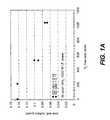
- FIG. 1Ais a graph showing how the ratio of side-wall to bottom dielectric growth varies with hydrogen gas flow rate.
- FIG. 1Bpresents 3 micrographs showing successively decreased void formation with increasing hydrogen gas flow rate.
- FIG. 2Ais a rough schematic cross-sectional diagram of a trench or via having problematic side-wall deposition of dielectric during HDP CVD.
- FIG. 2Bis a rough schematic cross-sectional diagram of a trench or via (as in FIG. 2A) having much less side-wall deposition of dielectric because the dielectric was grown with a hydrogen containing process gas.
- FIG. 3is a process flow diagram depicting a process context of the present invention.
- FIG. 4is a block diagram depicting some components of a suitable CVD reactor for performing HDP CVD in accordance with this invention.
- FIG. 5presents FTIR absorption spectra for silicon oxide dielectrics deposited by processes with and without hydrogen process gas.
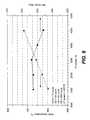
- FIG. 6is a graph showing that dielectric in-film stress is not compromised by employing hydrogen containing process gas.
- the present inventionrelates to chemical vapor deposition processes that can fill high aspect ratio (typically at least 3:1), narrow width (typically 1.5 microns or less and even sub 0.15 micron) gaps with significantly reduced incidence of voids or weak spots.
- This deposition processinvolves the use of hydrogen in the reactive mixture.
- this inventionpertains to improved high density plasma (HDP) chemical vapor deposition (CVD) processes.
- a high density plasmais any plasma having electron density of 5 ⁇ 10 9 electrons per cubic centimeter.
- high density plasma reactorsoperate at relatively low pressures, in the range of 100 mTorr or lower.
- FIG. 1Ais a graph showing how the ratio of side-wall to bottom dielectric growth improves with increasing hydrogen gas flow rate.
- the data shown in this figurewere taken from a Novellus SPEED reactor available from Novellus Systems, Inc. of San Jose, Calif. employing a low frequency (reactor electrode) power of 4000 Watts and a high frequency (substate) power of between 650 and 2900 Watts, depending on the amount of hydrogen. As the level of hydrogen was varied, the high frequency power was varied to maintain an effectively constant sputter to deposition ratio. Silicon oxide was deposited in 3.5:1 aspect ratio gaps of 0.13 micrometer widths.
- SD ratiorefers to the sputter/deposition ratio. It is obtained by measuring the deposition rate for a given dielectric deposition process and then measuring the sputter rate for that same process performed without the silicon-containing precursor (e.g., silane).
- the SD ratiois given by the following expression:
- the process gasincluded, in addition to varying amounts of hydrogen, 35 sccm SiH 4 , 47 sccm O 2 , and 40 sccm He (except in the cases where 0 sccm H 2 was used, in which case 100 sccm He was used).
- the deposition reactionproceeded under these conditions to a thickness of about 1550 Angstroms silicon dioxide measured at the field regions on a 200 millimeter wafer.
- the ratio of side-wall to bottom growth dielectric thicknessattained a maximum of slightly over 0.14 for process gases including either no hydrogen or 200 sccm hydrogen.
- process gasesincluding either no hydrogen or 200 sccm hydrogen.
- 500 sccm hydrogenwas introduced (together with the other gases), the ratio dropped to about 0.1.
- 1000 sccm hydrogenwas utilized, the ratio dropped further to about 0.065.
- the presence of hydrogen in the processreduces the relative amount of side-wall deposition.
- FIG. 1Bpresents 3 micro graphs showing successively decreased void formation with increasing hydrogen gas flow rate. For each of the three micrographs, the following process conditions were employed.
- Left-most structure0 sccm hydrogen, 180 sccm helium, 60 sccm silane, 78 sccm oxygen, 2500 Watts low frequency power, and 1200 Watts high frequency power.
- Middle structure400 sccm hydrogen, 40 sccm helium, 72 sccm silane, 94 sccm oxygen, 4000 Watts low frequency power, and 4200 Watts high frequency power.
- the voids left from the 400 sccm hydrogen processare significantly smaller than those left from the 0 sccm hydrogen process. Further, the voids essentially disappear when 1000 sccm hydrogen was employed.
- FIGS. 2A and 2Bshow in rough schematic fashion the variation in side-wall deposition that can be expected in a trench filled without hydrogen containing process gas (FIG. 2A) and with hydrogen containing process gas (FIG. 2 B).
- a HDP CVD processprovides a bottom fill.
- dielectric material 205 from the bottom of the trenchis sputtered by high momentum species from the plasma.
- Sputtered dielectric 207flies out toward the side-walls 209 .
- the sputtered speciesdo not significantly contribute to the growing side-wall coverage (dielectric) 211 .
- side-dielectric 211 ′rapidly grows in a lateral direction due to redeposition of the sputtered species 207 .
- Dielectricalso deposits on the field regions
- a deposition process 301begins at block 303 with a device (often a robot arm) delivering a substrate to a process chamber of a high-density plasma chemical vapor deposition reactor. Subsequently, the process will deposit dielectric on the substrate.
- Providing the substrate to the reactormay involve clamping the substrate to a pedestal or other support in the chamber. For this purpose, an electrostatic or mechanical chuck may be employed.
- the processprovides a preclean operation. See block 305 .
- Thisis intended to remove polymer or other residues in the gap prior to the dielectric film growing.
- thisis accomplished with a plasma phase reaction of at least one of an oxygen-containing gas and a hydrogen-containing gas.
- Oxygenis used for species that require oxidation and hydrogen is used for species that require reduction.
- the processadjusts the substrate temperature to a level promoting the deposition of the dielectric layer.
- this temperatureis between about 30-1000° C. (more preferably about 300 to 600° C.).
- the temperature control mechanismmay gradually raise the temperature during deposition or it may preheat the wafer to first drive out certain interfering species.
- the temperaturemay be maintained by supplying a heat transfer gas between a back surface of the substrate and a surface of the substrate holder on which the substrate is supported during the film growth operation.
- the processadjusts the pressure of the process chamber to a level suitable for the HDP CVD reaction. In some specific embodiments, this pressure is not greater than about 100 mTorr. The pressure should allow relatively rapid deposition while maintaining a high density plasma under the applied frequency and power.
- the reactor systemintroduces a process gas to the reaction chamber via an inlet.
- the process gasincludes dielectric precursor species such as high vapor pressure silicon-containing compounds and dopant precursors. Molecular oxygen or another oxygenated compound will often be present. Sometimes, though not necessarily, an inert carrier gas is present. Importantly, the introduced process gas also includes molecular elemental hydrogen. All the process gas components are introduced at specified flow rates.
- an electrical subsystemapplies electrical energy of appropriate power and frequency to one or more electrodes of the reaction chamber.
- the power and frequencyare chosen to generate a high-density plasma in the chamber, given the process gas concentration, pressure, and other process parameters.
- an electrical subsystemapplies a bias to the substrate, to thereby direct charged precursor species from the plasma onto the substrate and grow a dielectric film.
- the substrateitself serves as an electrode here. Its bias accelerates charged species to it.
- the substrate electrodeis powered by a high frequency rf bias and the other electrode is powered by a lower frequency rf source.
- the processis complete. After evacuating the chamber and adjusting the temperature and pressure as appropriate, the substrate may be removed for further processing.
- Suitable reactorsinclude the Novellus SPEED reactor, available from Novellus Systems, Inc. of San Jose, Calif., and the Ultima reactor, available from Applied Materials, Inc. of Santa Clara, Calif.
- reactorsinclude a reaction chamber, a process gas delivery system, a support for the substrate, one or more electrodes to generate a plasma and a bias source for the substrate.
- a temperature control systemis typically used to heat the substrate.
- FIG. 4provides a simple block diagram depicting various reactor components arranged as in a conventional reactor.
- a reactor 401includes a process chamber 403 which encloses other components of the reactor and serves to contain the plasma generated by an electrode 405 .
- the process chamber wallsare made from aluminum, aluminum oxide, and/or other suitable material.
- Electrode 405is powered by a “low frequency” rf source 406 . The power and frequency supplied by source 406 is sufficient to generate high-density plasma from the process gas.
- a wafer pedestal 407supports a substrate 409 .
- the pedestaltypically includes a chuck to hold the substrate in place during the deposition reaction.
- the chuckmay be an electrostatic chuck, a mechanical chuck or various other types of chuck as are available for use in the industry and/or research.
- a heat transfer subsystem including a line 411 for supplying a heat transfer fluidcontrols the temperature of substrate 409 .
- the heat transfer fluidcomprises at least one of helium and argon gas. Water or other liquid is used in other embodiments.
- the heat transfer fluidis supplied to a space 413 between the surface of the substrate and a surface of the chuck.
- a “high frequency” rf source 415serves to electrically bias substrate 409 and draw charged precursor species onto the substrate for the deposition reaction. Electrical energy from source 415 is coupled to substrate 409 via an electrode or capacitive coupling, for example. Note that the bias applied to the substrate need not be an rf bias. Other frequencies and DC bias may be used as well. In a specific embodiment, source 415 supplies a radio frequency bias to the substrate, and the radio frequency bias is generated by supplying the electrode with at least 0.2 W/cm 2 of power.
- the process gasesare introduced via one or more inlets 417 and 417 ′.
- the gasesmay be premixed or not.
- a source of elemental hydrogen gasprovides hydrogen for the process gas.
- Other sources of precursor gases and carrier gasesmay also be provided.
- the process gasis introduced through a gas supply inlet mechanism including orifices. In some embodiments, at least some of the orifices orient the process gas along an axis of injection intersecting an exposed surface of the substrate at an acute angle.
- the gas or gas mixturemay be introduced from a primary gas ring, which may or may not direct the gas toward the substrate surface. Injectors may be connected to the primary gas ring to direct at least some of the gas or gas mixture into the chamber and toward substrate. Note that injectors, gas rings or other mechanisms for directing process gas toward the wafer are not critical to this invention. The sonic front caused by the gas entering the chamber will itself cause the gas to rapidly disperse in all directions—including toward the substrate.
- a vacuum pumpe.g., a turbomolecular pump typically draws the gas out and maintains a suitably low pressure within the reactor.
- the process gas itselfwill have a particular composition. Each component will be present at a particular level. Typically, the composition is represented by flow rates of the constituent gases in units of standard cubic centimeter per minute (sccm).
- elemental hydrogenis introduced into the chamber as a process gas.
- the process gaswill also include a precursor for the deposition layer.
- the dielectricis a silicon-containing dielectric
- the process gaswill include a silicon-bearing compound such as SiH 4 , SiF 4 , Si 2 H 6 , TEOS (tetraethyl orthosilicate), TMCTS (tetramethyl-cyclotetrasiloxane), OMCTS (octamethyl-cyclotetrasiloxane), methyl-silane, dimethyl-silane, 3MS (trimethylsilane), 4MS (tetramethylsilane), TMDSO (tetramethyl-disiloxane), TMDDSO (tetramethyl-diethoxyl-disiloxane), DMDMS (dimethyl-dimethoxyl-silane) and mixtures thereof.
- the processdecomposes the silicon-containing reactant to form a silicon
- Oxygen to form the silicon oxide or other dielectric materialmay be provided by the silicon-containing precursor itself or from another process gas such as elemental oxygen (O 2 ), nitric oxide (NO), and/or nitrous oxide (N 2 O).
- elemental oxygenO 2
- NOnitric oxide
- N 2 Onitrous oxide
- the flow rate rangesmay have to be changed. While there are no precise rules for modifying flow rates as a function of molecular structure, generally the flow rate of the silicon-containing precursor may be reduced by a factor corresponding to the number of silicon atoms in the molecule. So, for example, if the molecule contains two silicon atoms, one may expect to reduce the flow rate of the silicon-containing precursor to a level of between about 5 and 125 sccm.
- the presence of hydrogen in the process gasmay require that the ratio of oxygen containing precursor to silicon-containing precursor be adjusted upward (in comparison to a standard hydrogen-free process), as hydrogen reacts with and removes the oxygen from the deposition reaction. Regardless of this process variation, it has been found that the presence of hydrogen in the process gas does not detrimentally affect the physical and material properties of the deposited dielectric film.
- the flow rate of hydrogen employedis at least about 200 sccm, and more preferably at least about 400 sccm, and most preferably at least about 500 sccm—all based on a 200 millimeter substrate. Larger substrates require higher flow rates. The flow rate may vary somewhat when special injector configurations are employed.
- the inventionis practiced with processes gases containing substantially no noble gas (e.g., argon, helium, or xenon).
- gases containing substantially no noble gase.g., argon, helium, or xenon.
- Other embodiments of the present inventioninclude the use of noble gas carriers such as argon, helium, and/or xenon.
- the use of noble gasescan be practiced under the conditions of the above-described embodiments.
- the process gasmay include a dopant precursor such as a boron-containing gas, a phosphorus-containing gas, or a mixture thereof.
- the gasincludes one or more boron-containing reactants and one or more phosphorus-containing reactants and the dielectric film includes a phosphorus- and boron-doped silicon oxide glass (BPSG).
- suitable boron and phosphorus precursor gasesinclude the following: B 2 H 6 and PH 3 .
- the process gaspreferably includes a fluorine-containing reactant such as silicon hexafluoride. If the dielectric is to contain an oxynitride (e.g., silicon oxynitride), then the process gas preferably includes a nitrogen-containing reactant such as N 2 , NH 3 , NF 3 , NO, N 2 O, and mixtures thereof.
- oxyfluoridee.g., silicon oxyfluoride
- the process gaspreferably includes a nitrogen-containing reactant such as N 2 , NH 3 , NF 3 , NO, N 2 O, and mixtures thereof.
- Reactor pressureis held at a value necessary to sustain the high-density plasma.
- the process vesselis maintained at a pressure of at most about 100 mTorr.
- the process chamber pressureis maintained below 1 mTorr.
- the pressureis maintained between about 1 and 100 mTorr; most preferably between about 1 and 30 mTorr.
- the temperature within the process vesselshould be maintained sufficiently high to ensure that the dielectric deposition reaction proceeds efficiently.
- the temperaturepreferably resides at values between about 30 and 1000° C. This temperature will vary depending upon the types of precursors employed in the reaction. Further, the temperature may be limited by process constraints, such as thermal budget limitations that preclude temperatures above 700-750° C. Such constraints become increasingly common with advanced technologies and corresponding smaller feature sizes.
- the process temperatureis preferably maintained between about 30 and 750° C.
- the substrate temperatureis maintained between about 300 and 600° C., even more preferably between about 350 and 450° C.
- the reactormay supply a heat transfer gas between a surface of the substrate and a surface of the substrate holder on which the substrate is supported during film deposition.
- the heat transfer gasmay include at least one of helium and argon.
- the back-side helium pressureis set by the temperature requirements of the process (a typical range being between 0-15 Torr).
- the low frequency power applied to the upper electrode (for generating the plasma)typically varies from 1 kW to 20 kW, and the high frequency power (for biasing the wafer) typically reaches at least about 0.2 W/cm 2 (preferably varying from about 0.5 kW to 10 kW) depending on the substrate size (e.g., 200 or 300 mm diameter) and the requirements of the specific process being used.
- the bias applied to the substrateis typically a radio frequency bias. Applying radio frequency bias to the substrate involves supporting the substrate on a substrate holder having an electrode supplying a radio frequency bias to the substrate.
- the radio frequency bias applied to the substrateis at the frequency range of between about 100 kHz and 27 MHz.
- the frequency range applied to the upper, plasma-generating electrodeis typically between about 300 kHz and 27 MHz.
- the above-described processes and apparatusesmay deposit dielectric on any type of substrate that requires thin dielectric layers.
- the substratewill be a semiconductor wafer having gaps in need of dielectric filling.
- the inventionis not, however, limited to such applications. It may be employed in a myriad of other fabrication processes such as for fabricating flat panel displays.
- the gap filling processesare performed on partially fabricated integrated circuits employing semiconductor substrates.
- the gap filling processes of this inventionare employed to form shallow trench isolation, inter-metal dielectric layers, passivation layers, etc.
- the inventioncan effectively fill gaps having widths of 1.5 micrometers or less and aspect ratios of 3:1 or greater. More aggressive structures having, e.g., greater aspect ratios and smaller widths may also be used. In one example the gap width is 0.15 micrometers or less.
- the dielectrics employed to fill those gapswill often be a silicon oxide such as silicon dioxide, silicon oxynitride, silicon oxyfluoride, and doped variants of each of these. Therefore, the scope of the invention includes at least fluorine-doped, phosphorus-doped, boron-doped, and boron/phosphorus-doped oxides. As indicated, the dielectric may also be a phosphorus- and boron-doped silicon oxide glass (BPSG).
- BPSGphosphorus- and boron-doped silicon oxide glass
- dielectricwas deposited on 622 separate wafers using hydrogen containing process gas.
- the process parameterswere as follows:
- the overall film thickness and refractive indexwere remarkably consistent from wafer to wafer. Further, the film thickness was found to vary by no more than about 2% within the wafer. And the film refractive index was found to vary by no more than about 0.1% within the wafer.
- FIG. 5shows an FTIR absorbance spectrum of a dielectric film deposited by a standard process (lower curve) and a hydrogen containing process (upper curve). Importantly, both curves have peaks at the same spectral locations and the ratios of those peaks (upper curve:lower curve) are identical. Also, note that there are no peaks associated with Si—H, H 2 O, or SiO—H. Each of these detrimental species could potentially form when hydrogen is present. The films were deposited using the conditions listed above.
Landscapes
- Engineering & Computer Science (AREA)
- Chemical & Material Sciences (AREA)
- Manufacturing & Machinery (AREA)
- Physics & Mathematics (AREA)
- Power Engineering (AREA)
- Microelectronics & Electronic Packaging (AREA)
- Computer Hardware Design (AREA)
- General Physics & Mathematics (AREA)
- Condensed Matter Physics & Semiconductors (AREA)
- Mechanical Engineering (AREA)
- Organic Chemistry (AREA)
- Metallurgy (AREA)
- Chemical Kinetics & Catalysis (AREA)
- Materials Engineering (AREA)
- General Chemical & Material Sciences (AREA)
- Inorganic Chemistry (AREA)
- Chemical Vapour Deposition (AREA)
- Formation Of Insulating Films (AREA)
Abstract
Description
This application claims priority from prior U.S. Provisional Patent Application No. 60/314,924, titled “GAP FILL FOR HIGH ASPECT RATIO STRUCTURES,” filed Aug. 24, 2001 by Bayman et al., which is incorporated herein by reference for all purposes.
This invention relates to electronic device fabrication processes and associated apparatus. More specifically, the invention relates to chemical vapor deposition processes for forming dielectric layers in high aspect ratio, narrow width recessed features.
It is often necessary in semiconductor processing to fill a high aspect ratio gaps with insulating material. This is the case for shallow trench isolation, inter-metal dielectric layers, passivation layers, etc. As device geometries shrink and thermal budgets are reduced, void-free filling of high aspect ratio spaces (e.g., AR>3.0:1) becomes increasingly difficult due to limitations of existing deposition processes.
Most deposition methods either deposit more material on the upper region than on the lower region of a side-wall or form cusps at the entry of the gap. As a result the top part of a high aspect ratio structure sometimes closes prematurely leaving voids within the gap's lower portions. This problem is exacerbated in small features. Furthermore, as aspect ratios increase, the shape of the gap itself can contribute to the problem. High aspect ratio gaps often exhibit reentrant features, which make gap filling even more difficult. The most problematic reentrant feature is a narrowing at the top of the gap. Thus, the etched side-walls slope inward near the top of the gap. For a given aspect ratio feature, this increases the ratio of gap volume to gap access area seen by the precursor species during deposition. Hence voids and seams become even more likely.
While some specific gap fill processes such as TEOS/ozone SACVD (sub atmospheric chemical vapor deposition) deposited BPSG provide generally good results, such processes are expiring due to incompatibility with the advanced device constraint of a maximum thermal budget of 700° C.
Going forward, the deposition of silicon dioxide assisted by high-density plasma chemical vapor deposition (HDP CVD)—a directional (bottom-up) CVD process—is the method of choice for high aspect ratio gap-fill. The method deposits more material at the bottom of a high aspect ratio structure than on its side-walls. It accomplishes this by directing charged dielectric precursor species downward, to the bottom of the gap. Thus, HDP CVD is not an entirely diffusion-based (isotropic) process.
Nevertheless, some overhang still results at the entry region of the gap to be filled. This results from the non-directional deposition reactions of neutral species in the plasma reactor and from sputtering/redeposition processes. The directional aspect of the deposition process produces some high momentum charged species that sputter away bottom fill. The sputtered material tends to redeposit on the side-walls. Thus, the formation of overhang cannot be totally eliminated and is inherent to the physics and chemistry of the HDP CVD process. Of course, limitations due to overhang formation become ever more severe as the width of the gap to be filled decreases, the aspect ratio increases, and the features become reentrant.
To improve fabrication of advanced technology devices, the art requires better dielectric deposition processes that can fill high aspect ratio features of narrow width, without leaving gaps.
This invention addresses that need by providing hydrogen as a process gas in a high density plasma CVD process. This process has been found to provide void free high-quality gap filling with dielectric materials. These benefits occur even in very narrow, high aspect ratio features.
One aspect of the invention provides a method of filling gaps on a semiconductor substrate. The method may be characterized by the following sequence: (a) providing a substrate in a process chamber of a high density plasma chemical vapor deposition reactor; (b) introducing a process gas including at least hydrogen into the process chamber; and (c) applying a bias to the substrate. This method will effectively grow a dielectric film on the semiconductor substrate via HDP CVD. This process effectively fills gaps having widths of less than about 1.5 micrometer.
The process gas preferably provides hydrogen at a flow rate of at least about 400 sccm. This value is based on a 200 millimeter substrate. Larger substrates may require correspondingly higher flow rates. The inventors have found that hydrogen flow rates in this regime provide significantly reduced side-wall dielectric redeposition during HDP CVD.
In an alternative preferred embodiment, the substrate is heated to a temperature of between about 300 and 600° C. and held in this temperature range during the deposition process. While improved results from hydrogen addition are present over a much wider range of temperatures, this temperature range in particular has been found to provide superior results.
In yet another preferred embodiment, the process gas contains substantially no noble gas (e.g., argon, helium, and/or xenon). In many conventional systems, noble gases are used as carrier gases for HDP CVD. Note that while many embodiments of this invention do in fact employ noble carrier gases, certain preferred embodiments require no noble gas.
To deposit dielectric, the carrier gas should include one or more dielectric precursors. In many commercially important embodiments, the dielectric is a silicon oxide or related material. For these embodiments, the process gas includes a volatile silicon-containing precursor, in addition to the hydrogen gas. Examples of such silicon-containing precursors include SiH4, SiF4, Si2H6, TEOS, TMCTS, OMCTS, methyl-silane, dimethyl-silane, 3MS, 4MS, TMDSO, TMDDSO, DMDMS and mixtures thereof. During deposition, the process decomposes the silicon-containing reactant to allow plasma phase reacting of the silicon-containing gas on the surface of the substrate.
To form silicon oxides, the process gas should also include a source of oxygen. Some silicon-containing precursors have some covalently bound oxygen (e.g., TEOS). However, additional oxygen is typically required, even for the oxygen-containing precursors. Hence, the process gas typically includes elemental oxygen or some other source of atomic oxygen such as nitrous oxide or nitric oxide.
To tailor the characteristics of the dielectric, various dopants or other modifiers may be provided. Examples of dopants include boron and phosphorus. The processes of this invention may provide these dopants via volatile phosphorus-containing process gases and/or volatile boron-containing process gases. The dielectric may also comprise a silicon oxynitride and/or a silicon oxyfluoride. Such materials may be made via processes of this invention that employ nitrogen-containing precursors (e.g., N2, N2O, NO, NH3, NF3) and/or fluorine-containing precursors.
The detailed description below will further discuss the benefits and features of this invention.
FIG. 1A is a graph showing how the ratio of side-wall to bottom dielectric growth varies with hydrogen gas flow rate.
FIG. 1B presents 3 micrographs showing successively decreased void formation with increasing hydrogen gas flow rate.
FIG. 2A is a rough schematic cross-sectional diagram of a trench or via having problematic side-wall deposition of dielectric during HDP CVD.
FIG. 2B is a rough schematic cross-sectional diagram of a trench or via (as in FIG. 2A) having much less side-wall deposition of dielectric because the dielectric was grown with a hydrogen containing process gas.
FIG. 3 is a process flow diagram depicting a process context of the present invention.
FIG. 4 is a block diagram depicting some components of a suitable CVD reactor for performing HDP CVD in accordance with this invention.
FIG. 5 presents FTIR absorption spectra for silicon oxide dielectrics deposited by processes with and without hydrogen process gas.
FIG. 6 is a graph showing that dielectric in-film stress is not compromised by employing hydrogen containing process gas.
The present invention relates to chemical vapor deposition processes that can fill high aspect ratio (typically at least 3:1), narrow width (typically 1.5 microns or less and even sub 0.15 micron) gaps with significantly reduced incidence of voids or weak spots. This deposition process involves the use of hydrogen in the reactive mixture.
Even though the formation of overhang and side-wall growth can not be entirely eliminated in chemical vapor deposition reactions employing plasma, film growth on the side-wall of the gap can be minimized and bottom-up fill enhanced by minimizing the sticking probability of fragments on the side-wall of the gap. Using hydrogen in the gas mixture seems to accomplish this. The addition of hydrogen likely impacts in a positive way the plasma and/or side-wall surface chemistry and species mobility resulting in improved gap-fill. Note that this invention is not limited to any particular mechanism of action in which the hydrogen participates.
As indicated, this invention pertains to improved high density plasma (HDP) chemical vapor deposition (CVD) processes. Generally, a high density plasma is any plasma having electron density of 5×10⁹electrons per cubic centimeter. Typically, though not necessarily, high density plasma reactors operate at relatively low pressures, in the range of 100 mTorr or lower.
FIG. 1A is a graph showing how the ratio of side-wall to bottom dielectric growth improves with increasing hydrogen gas flow rate. The data shown in this figure were taken from a Novellus SPEED reactor available from Novellus Systems, Inc. of San Jose, Calif. employing a low frequency (reactor electrode) power of 4000 Watts and a high frequency (substate) power of between 650 and 2900 Watts, depending on the amount of hydrogen. As the level of hydrogen was varied, the high frequency power was varied to maintain an effectively constant sputter to deposition ratio. Silicon oxide was deposited in 3.5:1 aspect ratio gaps of 0.13 micrometer widths.
Note that the data in FIG. 1A was taken for two different sets of process conditions, identified as SD ratio=0.14 and SD ratio=0.17. SD ratio refers to the sputter/deposition ratio. It is obtained by measuring the deposition rate for a given dielectric deposition process and then measuring the sputter rate for that same process performed without the silicon-containing precursor (e.g., silane). The SD ratio is given by the following expression:
In the FIG. 1A the process gas included, in addition to varying amounts of hydrogen, 35 sccm SiH4, 47 sccm O2, and 40 sccm He (except in the cases where 0 sccm H2was used, in which case 100 sccm He was used). The deposition reaction proceeded under these conditions to a thickness of about 1550 Angstroms silicon dioxide measured at the field regions on a 200 millimeter wafer.
As shown in the graph, the ratio of side-wall to bottom growth dielectric thickness attained a maximum of slightly over 0.14 for process gases including either no hydrogen or 200 sccm hydrogen. When 500 sccm hydrogen was introduced (together with the other gases), the ratio dropped to about 0.1. And when 1000 sccm hydrogen was utilized, the ratio dropped further to about 0.065. Clearly, the presence of hydrogen in the process reduces the relative amount of side-wall deposition.
FIG. 1B presents 3 micro graphs showing successively decreased void formation with increasing hydrogen gas flow rate. For each of the three micrographs, the following process conditions were employed.
Left-most structure: 0 sccm hydrogen, 180 sccm helium, 60 sccm silane, 78 sccm oxygen, 2500 Watts low frequency power, and 1200 Watts high frequency power.
Middle structure: 400 sccm hydrogen, 40 sccm helium, 72 sccm silane, 94 sccm oxygen, 4000 Watts low frequency power, and 4200 Watts high frequency power.
Right-most structure: 1000 sccm hydrogen, 40 sccm helium, 45 sccm silane, 62 sccm oxygen, 4000 Watts low frequency power, and 3800 Watts high frequency power.
As can be seen, the voids left from the 400 sccm hydrogen process are significantly smaller than those left from the 0 sccm hydrogen process. Further, the voids essentially disappear when 1000 sccm hydrogen was employed.
FIGS. 2A and 2B show in rough schematic fashion the variation in side-wall deposition that can be expected in a trench filled without hydrogen containing process gas (FIG. 2A) and with hydrogen containing process gas (FIG.2B). In both cases, a HDP CVD process provides a bottom fill. And in both cases,dielectric material 205 from the bottom of the trench is sputtered by high momentum species from the plasma. Sputtered dielectric207 flies out toward the side-walls 209. In the case of hydrogen containing process gas, the sputtered species do not significantly contribute to the growing side-wall coverage (dielectric)211. In the case of hydrogen-free process gas, however, side-dielectric211′ rapidly grows in a lateral direction due to redeposition of the sputteredspecies 207. Dielectric also deposits on the field regions
A general process context for the gap filling technology of this invention is depicted FIG.3. As shown, adeposition process 301 begins atblock 303 with a device (often a robot arm) delivering a substrate to a process chamber of a high-density plasma chemical vapor deposition reactor. Subsequently, the process will deposit dielectric on the substrate. Providing the substrate to the reactor may involve clamping the substrate to a pedestal or other support in the chamber. For this purpose, an electrostatic or mechanical chuck may be employed.
After the wafer is appropriately situated in the chamber, the process provides a preclean operation. Seeblock 305. This is intended to remove polymer or other residues in the gap prior to the dielectric film growing. Preferably, this is accomplished with a plasma phase reaction of at least one of an oxygen-containing gas and a hydrogen-containing gas. Oxygen is used for species that require oxidation and hydrogen is used for species that require reduction.
After the substrate has been appropriately cleaned, various other operations associated with dielectric deposition are performed. These operations are represented byreference numbers
Inblock 307, the process adjusts the substrate temperature to a level promoting the deposition of the dielectric layer. Typically, this temperature is between about 30-1000° C. (more preferably about 300 to 600° C.). The temperature control mechanism may gradually raise the temperature during deposition or it may preheat the wafer to first drive out certain interfering species. During deposition, the temperature may be maintained by supplying a heat transfer gas between a back surface of the substrate and a surface of the substrate holder on which the substrate is supported during the film growth operation.
Atblock 309, the process adjusts the pressure of the process chamber to a level suitable for the HDP CVD reaction. In some specific embodiments, this pressure is not greater than about 100 mTorr. The pressure should allow relatively rapid deposition while maintaining a high density plasma under the applied frequency and power.
Atblock 311, the reactor system introduces a process gas to the reaction chamber via an inlet. The process gas includes dielectric precursor species such as high vapor pressure silicon-containing compounds and dopant precursors. Molecular oxygen or another oxygenated compound will often be present. Sometimes, though not necessarily, an inert carrier gas is present. Importantly, the introduced process gas also includes molecular elemental hydrogen. All the process gas components are introduced at specified flow rates.
Atblock 313, an electrical subsystem applies electrical energy of appropriate power and frequency to one or more electrodes of the reaction chamber. The power and frequency are chosen to generate a high-density plasma in the chamber, given the process gas concentration, pressure, and other process parameters.
Finally, at315, an electrical subsystem applies a bias to the substrate, to thereby direct charged precursor species from the plasma onto the substrate and grow a dielectric film. Note that the substrate itself serves as an electrode here. Its bias accelerates charged species to it. Typically, the substrate electrode is powered by a high frequency rf bias and the other electrode is powered by a lower frequency rf source.
When the dielectric layer is deposited on the substrate to a desired thickness via the high density plasma chemical vapor deposition, the process is complete. After evacuating the chamber and adjusting the temperature and pressure as appropriate, the substrate may be removed for further processing.
Various plasma reactor designs are suitable for use with this invention. The particular design is not critical to this invention. It merely needs to support HDP CVD dielectric layer formation on appropriate substrates. Examples of suitable reactors include the Novellus SPEED reactor, available from Novellus Systems, Inc. of San Jose, Calif., and the Ultima reactor, available from Applied Materials, Inc. of Santa Clara, Calif.
The principal components of most suitable reactors include a reaction chamber, a process gas delivery system, a support for the substrate, one or more electrodes to generate a plasma and a bias source for the substrate. A temperature control system is typically used to heat the substrate.
FIG. 4 provides a simple block diagram depicting various reactor components arranged as in a conventional reactor. As shown, areactor 401 includes aprocess chamber 403 which encloses other components of the reactor and serves to contain the plasma generated by anelectrode 405. In one example, the process chamber walls are made from aluminum, aluminum oxide, and/or other suitable material.Electrode 405 is powered by a “low frequency”rf source 406. The power and frequency supplied bysource 406 is sufficient to generate high-density plasma from the process gas.
Within the reactor, awafer pedestal 407 supports asubstrate 409. The pedestal typically includes a chuck to hold the substrate in place during the deposition reaction. The chuck may be an electrostatic chuck, a mechanical chuck or various other types of chuck as are available for use in the industry and/or research.
A heat transfer subsystem including aline 411 for supplying a heat transfer fluid controls the temperature ofsubstrate 409. In some embodiments, the heat transfer fluid comprises at least one of helium and argon gas. Water or other liquid is used in other embodiments. The heat transfer fluid is supplied to aspace 413 between the surface of the substrate and a surface of the chuck.
A “high frequency”rf source 415 serves to electricallybias substrate 409 and draw charged precursor species onto the substrate for the deposition reaction. Electrical energy fromsource 415 is coupled tosubstrate 409 via an electrode or capacitive coupling, for example. Note that the bias applied to the substrate need not be an rf bias. Other frequencies and DC bias may be used as well. In a specific embodiment,source 415 supplies a radio frequency bias to the substrate, and the radio frequency bias is generated by supplying the electrode with at least 0.2 W/cm2of power.
The process gases are introduced via one ormore inlets
The process gas exitschamber 403 via anoutlet 419. A vacuum pump (e.g., a turbomolecular pump) typically draws the gas out and maintains a suitably low pressure within the reactor.
The process gas itself will have a particular composition. Each component will be present at a particular level. Typically, the composition is represented by flow rates of the constituent gases in units of standard cubic centimeter per minute (sccm).
In all embodiments of this invention, elemental hydrogen is introduced into the chamber as a process gas. The process gas will also include a precursor for the deposition layer. If the dielectric is a silicon-containing dielectric, then the process gas will include a silicon-bearing compound such as SiH4, SiF4, Si2H6, TEOS (tetraethyl orthosilicate), TMCTS (tetramethyl-cyclotetrasiloxane), OMCTS (octamethyl-cyclotetrasiloxane), methyl-silane, dimethyl-silane, 3MS (trimethylsilane), 4MS (tetramethylsilane), TMDSO (tetramethyl-disiloxane), TMDDSO (tetramethyl-diethoxyl-disiloxane), DMDMS (dimethyl-dimethoxyl-silane) and mixtures thereof. During deposition, the process decomposes the silicon-containing reactant to form a silicon-containing gas and plasma phase species, which can react on the surface of the substrate.
Oxygen to form the silicon oxide or other dielectric material may be provided by the silicon-containing precursor itself or from another process gas such as elemental oxygen (O2), nitric oxide (NO), and/or nitrous oxide (N2O).
Typical flow rate ranges for process gases of the present invention are listed below.
| Gas | Flow Rate (sccm) | ||
| SiH4 | 10-250 | ||
| O2 | 10-1000 | ||
| H2 | 10-5000 | ||
Generally, other oxygen and silicon-containing compounds can be substituted for those listed in this table. Depending upon the atom counts in the precursor gases, the flow rate ranges may have to be changed. While there are no precise rules for modifying flow rates as a function of molecular structure, generally the flow rate of the silicon-containing precursor may be reduced by a factor corresponding to the number of silicon atoms in the molecule. So, for example, if the molecule contains two silicon atoms, one may expect to reduce the flow rate of the silicon-containing precursor to a level of between about 5 and 125 sccm.
Note also that the presence of hydrogen in the process gas may require that the ratio of oxygen containing precursor to silicon-containing precursor be adjusted upward (in comparison to a standard hydrogen-free process), as hydrogen reacts with and removes the oxygen from the deposition reaction. Regardless of this process variation, it has been found that the presence of hydrogen in the process gas does not detrimentally affect the physical and material properties of the deposited dielectric film.
In preferred embodiments, the flow rate of hydrogen employed is at least about 200 sccm, and more preferably at least about 400 sccm, and most preferably at least about 500 sccm—all based on a 200 millimeter substrate. Larger substrates require higher flow rates. The flow rate may vary somewhat when special injector configurations are employed.
In certain preferred embodiments, the invention is practiced with processes gases containing substantially no noble gas (e.g., argon, helium, or xenon). Other embodiments of the present invention, however, include the use of noble gas carriers such as argon, helium, and/or xenon. The use of noble gases can be practiced under the conditions of the above-described embodiments.
For doped dielectrics (particularly silicon dioxide based dielectrics), the process gas may include a dopant precursor such as a boron-containing gas, a phosphorus-containing gas, or a mixture thereof. In a specific embodiment, the gas includes one or more boron-containing reactants and one or more phosphorus-containing reactants and the dielectric film includes a phosphorus- and boron-doped silicon oxide glass (BPSG). Examples of suitable boron and phosphorus precursor gases include the following: B2H6and PH3.
If the dielectric is to contain an oxyfluoride (e.g., silicon oxyfluoride), then the process gas preferably includes a fluorine-containing reactant such as silicon hexafluoride. If the dielectric is to contain an oxynitride (e.g., silicon oxynitride), then the process gas preferably includes a nitrogen-containing reactant such as N2, NH3, NF3, NO, N2O, and mixtures thereof.
Reactor pressure is held at a value necessary to sustain the high-density plasma. Preferably the process vessel is maintained at a pressure of at most about 100 mTorr. In some cases, the process chamber pressure is maintained below 1 mTorr. For many applications, however, the pressure is maintained between about 1 and 100 mTorr; most preferably between about 1 and 30 mTorr.
The temperature within the process vessel should be maintained sufficiently high to ensure that the dielectric deposition reaction proceeds efficiently. Hence, the temperature preferably resides at values between about 30 and 1000° C. This temperature will vary depending upon the types of precursors employed in the reaction. Further, the temperature may be limited by process constraints, such as thermal budget limitations that preclude temperatures above 700-750° C. Such constraints become increasingly common with advanced technologies and corresponding smaller feature sizes. For such applications, the process temperature is preferably maintained between about 30 and 750° C. In particularly preferred embodiments, the substrate temperature is maintained between about 300 and 600° C., even more preferably between about 350 and 450° C.
As indicated, to control the substrate temperature, the reactor may supply a heat transfer gas between a surface of the substrate and a surface of the substrate holder on which the substrate is supported during film deposition. The heat transfer gas may include at least one of helium and argon. The back-side helium pressure is set by the temperature requirements of the process (a typical range being between 0-15 Torr).
For some applications, it may be desirable to preheat the wafer to a pre-specified relatively low temperature and then gradually raise the temperature. This allows for isothermal operation. The goal is to start the deposition and then maintain the wafer temperature within a narrow range during the entire deposition process.
The low frequency power applied to the upper electrode (for generating the plasma) typically varies from 1 kW to 20 kW, and the high frequency power (for biasing the wafer) typically reaches at least about 0.2 W/cm2(preferably varying from about 0.5 kW to 10 kW) depending on the substrate size (e.g., 200 or 300 mm diameter) and the requirements of the specific process being used.
As indicated above, the bias applied to the substrate is typically a radio frequency bias. Applying radio frequency bias to the substrate involves supporting the substrate on a substrate holder having an electrode supplying a radio frequency bias to the substrate. For many embodiments, the radio frequency bias applied to the substrate is at the frequency range of between about 100 kHz and 27 MHz. The frequency range applied to the upper, plasma-generating electrode is typically between about 300 kHz and 27 MHz.
The above-described processes and apparatuses may deposit dielectric on any type of substrate that requires thin dielectric layers. Often, the substrate will be a semiconductor wafer having gaps in need of dielectric filling. The invention is not, however, limited to such applications. It may be employed in a myriad of other fabrication processes such as for fabricating flat panel displays.
As indicated above, this invention finds particular value in integrated circuit fabrication. The gap filling processes are performed on partially fabricated integrated circuits employing semiconductor substrates. In specific examples, the gap filling processes of this invention are employed to form shallow trench isolation, inter-metal dielectric layers, passivation layers, etc.
As indicated, the invention can effectively fill gaps having widths of 1.5 micrometers or less and aspect ratios of 3:1 or greater. More aggressive structures having, e.g., greater aspect ratios and smaller widths may also be used. In one example the gap width is 0.15 micrometers or less.
The dielectrics employed to fill those gaps will often be a silicon oxide such as silicon dioxide, silicon oxynitride, silicon oxyfluoride, and doped variants of each of these. Therefore, the scope of the invention includes at least fluorine-doped, phosphorus-doped, boron-doped, and boron/phosphorus-doped oxides. As indicated, the dielectric may also be a phosphorus- and boron-doped silicon oxide glass (BPSG).
To test the hydrogen gas process, dielectric was deposited on 622 separate wafers using hydrogen containing process gas. The process parameters were as follows:
| SiH4 | 35 sccm | ||
| O2 | 65 sccm | ||
| He | 40 | ||
| H | |||
| 2 | 1000 | ||
| LF Power | |||
| 4000 | |||
| HF Power | |||
| 3000 Watts | |||
| Depo. Time | 193 seconds | ||
Under these conditions, it was found that the overall film thickness and refractive index were remarkably consistent from wafer to wafer. Further, the film thickness was found to vary by no more than about 2% within the wafer. And the film refractive index was found to vary by no more than about 0.1% within the wafer.
FIG. 5 shows an FTIR absorbance spectrum of a dielectric film deposited by a standard process (lower curve) and a hydrogen containing process (upper curve). Importantly, both curves have peaks at the same spectral locations and the ratios of those peaks (upper curve:lower curve) are identical. Also, note that there are no peaks associated with Si—H, H2O, or SiO—H. Each of these detrimental species could potentially form when hydrogen is present. The films were deposited using the conditions listed above.
FIG. 6 shows in-film stress measurements for dielectric films deposited under the following conditions: SiH4=72 sccm, O2=94 sccm, He=40 sccm, H2=500 sccm, and low frequency power=4000 Watts. As shown, the film stress remains at about 230 MPa over a wide range of wafer temperatures (used in during processing). These numbers are consistent with those derived by standard chemistry processes.
While this invention has been described in terms of a few preferred embodiments, it should not be limited to the specifics presented above. Many variations on the above-described preferred embodiments, may be employed. Therefore, the invention should be broadly interpreted with reference to the following claims.
Claims (26)
1. A method of filling gaps on a semiconductor substrate, the method comprising
providing a substrate in a process chamber of a high density plasma chemical vapor deposition reactor;
introducing a process gas comprising at least about 400 sccm hydrogen into the process chamber; and
applying a bias to the substrate, to thereby grow a dielectric film via high density plasma chemical vapor deposition on the semiconductor substrate, wherein the dielectric film fills gaps with a width of less than about 1.5 micrometer.
2. The method ofclaim 1 , wherein the process gas further comprises a silicon-bearing compound selected from the group of SiH4, SiF4, Si2H6, TEOS, TMCTS, OMCTS, methyl-silane, dimethyl-silane, 3MS, 4MS, TMDSO, TMDDSO, DMDMS and mixtures thereof, said process further comprising decomposing the silicon-containing compound to allow plasma phase reacting of a silicon-containing reactant on the surface of the substrate.
3. The method ofclaim 2 , wherein the process gas further comprises a reactant selected from the group consisting of N2, N2O, NO, NH3, NF3, O2, and mixtures thereof.
4. The method ofclaim 3 , wherein the process gas comprises a reactant selected from the group of boron-containing gas, phosphorus-containing gas, and mixtures thereof.
5. The method ofclaim 1 , wherein the process chamber is maintained at a pressure of not more than about 100 mTorr.
6. The method ofclaim 1 , wherein the high-density plasma chemical vapor deposition reactor comprises an electrode that generates a plasma from the process gas.
7. The method ofclaim 1 , wherein the bias applied to the substrate is a radio frequency bias.
8. The method ofclaim 7 , wherein applying a bias to the substrate comprises supporting the substrate on a substrate holder having an electrode supplying a radio frequency bias to the substrate, the radio frequency bias being generated by supplying the electrode with at least 0.2 W/cm2of power.
9. The method ofclaim 7 , wherein the radio frequency bias applied to the substrate is at the frequency range of between about 100 kHz and 27 MHz.
10. The method ofclaim 1 , wherein the substrate is placed on a substrate holder that is maintained at a temperature of between about 30 and 1000° C.
11. The method ofclaim 1 , further comprising supplying a heat transfer gas between a surface of the substrate and a surface of the substrate holder on which the substrate is supported during the film growing.
12. The method ofclaim 11 , further comprising clamping the substrate on an electrostatic or mechanical chuck during the film growing.
13. The method ofclaim 12 , wherein the heat transfer gas comprises at least one of helium and argon and is supplied to a space between the surface of the substrate and a surface of the chuck.
14. The method ofclaim 1 , further comprising plasma phase reacting at least one of an oxygen-containing gas and a hydrogen-containing gas in the gaps and removing polymer residues in the gap prior to the film growing.
15. The method ofclaim 1 , wherein the dielectric film comprises a silicon oxide.
16. The method ofclaim 1 , wherein the dielectric film comprises SiO2.
17. The method ofclaim 1 , wherein the gas includes silicon and fluorine-containing reactants and the dielectric film comprises silicon oxyfluoride.
18. The method ofclaim 1 , wherein the gas includes nitrogen-containing reactants and the dielectric film comprises silicon oxynitride.
19. The method ofclaim 1 , wherein the gas includes phosphorus-containing reactants and the dielectric film comprises phosphorus-doped silicon oxide.
20. The method ofclaim 1 , wherein the gas includes boron-containing reactants and the dielectric film comprises boron-doped silicon oxide.
21. The method ofclaim 1 , wherein the gas includes boron-containing reactants and phosphorus-containing reactants and the dielectric film comprises phosphorus- and boron-doped silicon oxide (BPSG).
22. The method ofclaim 1 , wherein the process gas is introduced through a gas supply including orifices, at least some of the orifices orienting the process gas along an axis of injection intersecting an exposed surfaced of the substrate at an acute angle.
23. The method ofclaim 22 , wherein introducing the process gas comprises supplying a gas or gas mixture from a primary gas ring, wherein at least some of said gas or gas mixture is directed toward said substrate.
24. The method ofclaim 23 , wherein injectors are connected to said primary gas ring, the injectors injecting at least some of said gas or gas mixture into said chamber and directed toward substrate.
25. The method ofclaim 1 , wherein the gap filling method is employed to form shallow trench isolation (STI) regions.
26. The method ofclaim 1 , wherein the width of the gaps are 0.15 micrometers or less.
Priority Applications (5)
| Application Number | Priority Date | Filing Date | Title |
|---|---|---|---|
| US09/996,619US6596654B1 (en) | 2001-08-24 | 2001-11-28 | Gap fill for high aspect ratio structures |
| US10/058,897US6846745B1 (en) | 2001-08-03 | 2002-01-28 | High-density plasma process for filling high aspect ratio structures |
| US10/271,333US7001854B1 (en) | 2001-08-03 | 2002-10-11 | Hydrogen-based phosphosilicate glass process for gap fill of high aspect ratio structures |
| US10/442,846US6787483B1 (en) | 2001-08-24 | 2003-05-20 | Gap fill for high aspect ratio structures |
| US10/890,655US7067440B1 (en) | 2001-08-24 | 2004-07-13 | Gap fill for high aspect ratio structures |
Applications Claiming Priority (2)
| Application Number | Priority Date | Filing Date | Title |
|---|---|---|---|
| US31492401P | 2001-08-24 | 2001-08-24 | |
| US09/996,619US6596654B1 (en) | 2001-08-24 | 2001-11-28 | Gap fill for high aspect ratio structures |
Related Child Applications (3)
| Application Number | Title | Priority Date | Filing Date |
|---|---|---|---|
| US10/058,897Continuation-In-PartUS6846745B1 (en) | 2001-08-03 | 2002-01-28 | High-density plasma process for filling high aspect ratio structures |
| US10/271,333Continuation-In-PartUS7001854B1 (en) | 2001-08-03 | 2002-10-11 | Hydrogen-based phosphosilicate glass process for gap fill of high aspect ratio structures |
| US10/442,846DivisionUS6787483B1 (en) | 2001-08-24 | 2003-05-20 | Gap fill for high aspect ratio structures |
Publications (1)
| Publication Number | Publication Date |
|---|---|
| US6596654B1true US6596654B1 (en) | 2003-07-22 |
Family
ID=26979625
Family Applications (2)
| Application Number | Title | Priority Date | Filing Date |
|---|---|---|---|
| US09/996,619Expired - LifetimeUS6596654B1 (en) | 2001-08-03 | 2001-11-28 | Gap fill for high aspect ratio structures |
| US10/442,846Expired - LifetimeUS6787483B1 (en) | 2001-08-24 | 2003-05-20 | Gap fill for high aspect ratio structures |
Family Applications After (1)
| Application Number | Title | Priority Date | Filing Date |
|---|---|---|---|
| US10/442,846Expired - LifetimeUS6787483B1 (en) | 2001-08-24 | 2003-05-20 | Gap fill for high aspect ratio structures |
Country Status (1)
| Country | Link |
|---|---|
| US (2) | US6596654B1 (en) |
Cited By (276)
| Publication number | Priority date | Publication date | Assignee | Title |
|---|---|---|---|---|
| US20030159656A1 (en)* | 2001-05-11 | 2003-08-28 | Applied Materials, Inc. | Hydrogen assisted undoped silicon oxide deposition process for HDP-CVD |
| US20030203637A1 (en)* | 2002-04-30 | 2003-10-30 | Applied Materials, Inc. | Method for high aspect ratio HDP CVD gapfill |
| US20030207580A1 (en)* | 2002-05-03 | 2003-11-06 | Applied Materials, Inc. | HDP-CVD dep/etch/dep process for improved deposition into high aspect ratio features |
| US20040079728A1 (en)* | 2002-10-23 | 2004-04-29 | Applied Materials, Inc. | Reactive ion etching for semiconductor device feature topography modification |
| US20040079632A1 (en)* | 2002-10-23 | 2004-04-29 | Applied Materials, Inc. | High density plasma CVD process for gapfill into high aspect ratio features |
| US20040115898A1 (en)* | 2002-12-13 | 2004-06-17 | Applied Materials, Inc. | Deposition process for high aspect ratio trenches |
| US20040146661A1 (en)* | 2003-01-23 | 2004-07-29 | Applied Materials, Inc. | Hydrogen assisted hdp-cvd deposition process for aggressive gap-fill technology |
| US20040224090A1 (en)* | 2003-05-09 | 2004-11-11 | Applied Materials, Inc. | HDP-CVD uniformity control |
| US20040241342A1 (en)* | 2003-05-27 | 2004-12-02 | Applied Materials, Inc. | Methods and systems for high-aspect-ratio gapfill using atomic-oxygen generation |
| US20040245091A1 (en)* | 2003-06-04 | 2004-12-09 | Applied Materials, Inc. | Hdp-cvd multistep gapfill process |
| US20040251236A1 (en)* | 2003-05-23 | 2004-12-16 | Applied Materials, Inc. | [deposition-selective etch-deposition process for dielectric film gapfill] |
| US20050009291A1 (en)* | 2003-07-11 | 2005-01-13 | Jingyi Bai | Methods for filling high aspect ratio trenches in semiconductor layers |
| US20050019494A1 (en)* | 2003-07-25 | 2005-01-27 | Applied Materials, Inc., A Delaware Corporation | Sequential gas flow oxide deposition technique |
| US20050048801A1 (en)* | 2003-09-03 | 2005-03-03 | Applied Materials, Inc. | In-situ-etch-assisted HDP deposition using SiF4 and hydrogen |
| US20050074946A1 (en)* | 2003-10-02 | 2005-04-07 | Hsiu-Chuan Chu | [silicon oxide gap-filling process] |
| US20050196929A1 (en)* | 2004-03-04 | 2005-09-08 | Applied Materials, Inc., A Delaware Corporation | Low-thermal-budget gapfill process |
| US20050260356A1 (en)* | 2004-05-18 | 2005-11-24 | Applied Materials, Inc. | Microcontamination abatement in semiconductor processing |
| US20050277265A1 (en)* | 2004-06-11 | 2005-12-15 | Yong-Won Cha | Methods of forming trench isolation layers using high density plasma chemical vapor deposition |
| US20050282398A1 (en)* | 2004-06-16 | 2005-12-22 | Applied Materials, Inc., A Delaware Corporation | Oxygen plasma treatment for enhanced HDP-CVD gapfill |
| US7001854B1 (en) | 2001-08-03 | 2006-02-21 | Novellus Systems, Inc. | Hydrogen-based phosphosilicate glass process for gap fill of high aspect ratio structures |
| US20060046508A1 (en)* | 2004-09-01 | 2006-03-02 | Applied Materials, Inc. A Delaware Corporation | Silicon oxide gapfill deposition using liquid precursors |
| US7067440B1 (en)* | 2001-08-24 | 2006-06-27 | Novellus Systems, Inc. | Gap fill for high aspect ratio structures |
| US20060154494A1 (en)* | 2005-01-08 | 2006-07-13 | Applied Materials, Inc., A Delaware Corporation | High-throughput HDP-CVD processes for advanced gapfill applications |
| US7078312B1 (en) | 2003-09-02 | 2006-07-18 | Novellus Systems, Inc. | Method for controlling etch process repeatability |
| US20060156934A1 (en)* | 2003-09-19 | 2006-07-20 | Gallus Druckmaschinen Ag | Rotary printing press |
| US7094713B1 (en) | 2004-03-11 | 2006-08-22 | Novellus Systems, Inc. | Methods for improving the cracking resistance of low-k dielectric materials |
| US20060225648A1 (en)* | 2004-07-01 | 2006-10-12 | Applied Materials, Inc. | Use of enhanced turbomolecular pump for gapfill deposition using high flows of low-mass fluent gas |
| US7122485B1 (en)* | 2002-12-09 | 2006-10-17 | Novellus Systems, Inc. | Deposition profile modification through process chemistry |
| US20060292894A1 (en)* | 2005-06-24 | 2006-12-28 | Applied Materials, Inc., | Gapfill using deposition-etch sequence |
| US7163896B1 (en) | 2003-12-10 | 2007-01-16 | Novellus Systems, Inc. | Biased H2 etch process in deposition-etch-deposition gap fill |
| US7166531B1 (en) | 2005-01-31 | 2007-01-23 | Novellus Systems, Inc. | VLSI fabrication processes for introducing pores into dielectric materials |
| US7176144B1 (en) | 2003-03-31 | 2007-02-13 | Novellus Systems, Inc. | Plasma detemplating and silanol capping of porous dielectric films |
| US7176039B1 (en) | 2004-09-21 | 2007-02-13 | Novellus Systems, Inc. | Dynamic modification of gap fill process characteristics |
| US7196021B2 (en) | 2001-05-11 | 2007-03-27 | Applied Materials, Inc. | HDP-CVD deposition process for filling high aspect ratio gaps |
| US7208389B1 (en) | 2003-03-31 | 2007-04-24 | Novellus Systems, Inc. | Method of porogen removal from porous low-k films using UV radiation |
| US7211525B1 (en) | 2005-03-16 | 2007-05-01 | Novellus Systems, Inc. | Hydrogen treatment enhanced gap fill |
| US7217658B1 (en) | 2004-09-07 | 2007-05-15 | Novellus Systems, Inc. | Process modulation to prevent structure erosion during gap fill |
| US20070128865A1 (en)* | 2005-12-06 | 2007-06-07 | Kabushiki Kaisha Toshiba | Method of forming insulating film, method of manufacturing semiconductor device and their controlling computer program |
| US7241704B1 (en) | 2003-03-31 | 2007-07-10 | Novellus Systems, Inc. | Methods for producing low stress porous low-k dielectric materials using precursors with organic functional groups |
| US7253125B1 (en) | 2004-04-16 | 2007-08-07 | Novellus Systems, Inc. | Method to improve mechanical strength of low-k dielectric film using modulated UV exposure |
| US7265061B1 (en) | 2003-05-09 | 2007-09-04 | Novellus Systems, Inc. | Method and apparatus for UV exposure of low dielectric constant materials for porogen removal and improved mechanical properties |
| US20070277734A1 (en)* | 2006-05-30 | 2007-12-06 | Applied Materials, Inc. | Process chamber for dielectric gapfill |
| US20070281496A1 (en)* | 2006-05-30 | 2007-12-06 | Applied Materials, Inc. | Chemical vapor deposition of high quality flow-like silicon dioxide using a silicon containing precursor and atomic oxygen |
| US20070281448A1 (en)* | 2006-05-30 | 2007-12-06 | Applied Materials, Inc. | Novel deposition-plasma cure cycle process to enhance film quality of silicon dioxide |
| US20080026597A1 (en)* | 2006-05-30 | 2008-01-31 | Applied Materials, Inc. | Method for depositing and curing low-k films for gapfill and conformal film applications |
| US7326444B1 (en) | 2004-09-14 | 2008-02-05 | Novellus Systems, Inc. | Methods for improving integration performance of low stress CDO films |
| US7341761B1 (en) | 2004-03-11 | 2008-03-11 | Novellus Systems, Inc. | Methods for producing low-k CDO films |
| US7344996B1 (en) | 2005-06-22 | 2008-03-18 | Novellus Systems, Inc. | Helium-based etch process in deposition-etch-deposition gap fill |
| US7381451B1 (en) | 2004-11-17 | 2008-06-03 | Novellus Systems, Inc. | Strain engineering—HDP thin film with tensile stress for FEOL and other applications |
| US7381662B1 (en) | 2004-03-11 | 2008-06-03 | Novellus Systems, Inc. | Methods for improving the cracking resistance of low-k dielectric materials |
| US7381644B1 (en) | 2005-12-23 | 2008-06-03 | Novellus Systems, Inc. | Pulsed PECVD method for modulating hydrogen content in hard mask |
| US20080142483A1 (en)* | 2006-12-07 | 2008-06-19 | Applied Materials, Inc. | Multi-step dep-etch-dep high density plasma chemical vapor deposition processes for dielectric gapfills |
| US7390537B1 (en) | 2003-11-20 | 2008-06-24 | Novellus Systems, Inc. | Methods for producing low-k CDO films with low residual stress |
| US20080182382A1 (en)* | 2006-12-07 | 2008-07-31 | Applied Materials, Inc. | Methods of thin film process |
| US20080206956A1 (en)* | 2007-02-26 | 2008-08-28 | Taketo Matsuda | Semiconductor device fabrication method |
| US7476621B1 (en) | 2003-12-10 | 2009-01-13 | Novellus Systems, Inc. | Halogen-free noble gas assisted H2 plasma etch process in deposition-etch-deposition gap fill |
| US7482245B1 (en) | 2006-06-20 | 2009-01-27 | Novellus Systems, Inc. | Stress profile modulation in STI gap fill |
| US20090061647A1 (en)* | 2007-08-27 | 2009-03-05 | Applied Materials, Inc. | Curing methods for silicon dioxide thin films deposited from alkoxysilane precursor with harp ii process |
| US7510982B1 (en) | 2005-01-31 | 2009-03-31 | Novellus Systems, Inc. | Creation of porosity in low-k films by photo-disassociation of imbedded nanoparticles |
| US20090104755A1 (en)* | 2007-10-22 | 2009-04-23 | Applied Materials, Inc. | High quality silicon oxide films by remote plasma cvd from disilane precursors |
| US20090104790A1 (en)* | 2007-10-22 | 2009-04-23 | Applied Materials, Inc. | Methods for Forming a Dielectric Layer Within Trenches |
| US20090104791A1 (en)* | 2007-10-22 | 2009-04-23 | Applied Materials, Inc. A Delaware Corporation | Methods for Forming a Silicon Oxide Layer Over a Substrate |
| US7524750B2 (en) | 2006-04-17 | 2009-04-28 | Applied Materials, Inc. | Integrated process modulation (IPM) a novel solution for gapfill with HDP-CVD |
| US20090163041A1 (en)* | 2007-12-21 | 2009-06-25 | Applied Materials, Inc. | Low wet etch rate silicon nitride film |
| US20090286381A1 (en)* | 2008-05-16 | 2009-11-19 | Novellus Systems Inc. | Protective Layer To Enable Damage Free Gap Fill |
| US7622400B1 (en) | 2004-05-18 | 2009-11-24 | Novellus Systems, Inc. | Method for improving mechanical properties of low dielectric constant materials |
| US7622162B1 (en) | 2007-06-07 | 2009-11-24 | Novellus Systems, Inc. | UV treatment of STI films for increasing tensile stress |
| US7695765B1 (en) | 2004-11-12 | 2010-04-13 | Novellus Systems, Inc. | Methods for producing low-stress carbon-doped oxide films with improved integration properties |
| US20100159711A1 (en)* | 2008-12-18 | 2010-06-24 | Applied Materials, Inc. | Precursor addition to silicon oxide cvd for improved low temperature gapfill |
| US7781351B1 (en) | 2004-04-07 | 2010-08-24 | Novellus Systems, Inc. | Methods for producing low-k carbon doped oxide films with low residual stress |
| US7790633B1 (en) | 2004-10-26 | 2010-09-07 | Novellus Systems, Inc. | Sequential deposition/anneal film densification method |
| US7851232B2 (en) | 2006-10-30 | 2010-12-14 | Novellus Systems, Inc. | UV treatment for carbon-containing low-k dielectric repair in semiconductor processing |
| US20110034035A1 (en)* | 2009-08-06 | 2011-02-10 | Applied Materials, Inc. | Stress management for tensile films |
| US7892985B1 (en) | 2005-11-15 | 2011-02-22 | Novellus Systems, Inc. | Method for porogen removal and mechanical strength enhancement of low-k carbon doped silicon oxide using low thermal budget microwave curing |
| US7906174B1 (en) | 2006-12-07 | 2011-03-15 | Novellus Systems, Inc. | PECVD methods for producing ultra low-k dielectric films using UV treatment |
| US7923376B1 (en) | 2006-03-30 | 2011-04-12 | Novellus Systems, Inc. | Method of reducing defects in PECVD TEOS films |
| US20110117678A1 (en)* | 2006-10-30 | 2011-05-19 | Varadarajan Bhadri N | Carbon containing low-k dielectric constant recovery using uv treatment |
| US7951683B1 (en) | 2007-04-06 | 2011-05-31 | Novellus Systems, Inc | In-situ process layer using silicon-rich-oxide for etch selectivity in high AR gapfill |
| US7989365B2 (en) | 2009-08-18 | 2011-08-02 | Applied Materials, Inc. | Remote plasma source seasoning |
| US7994019B1 (en) | 2010-04-01 | 2011-08-09 | Applied Materials, Inc. | Silicon-ozone CVD with reduced pattern loading using incubation period deposition |
| US8030172B1 (en)* | 2000-09-12 | 2011-10-04 | Cypress Semiconductor Corporation | Isolation technology for submicron semiconductor devices |
| US8110493B1 (en) | 2005-12-23 | 2012-02-07 | Novellus Systems, Inc. | Pulsed PECVD method for modulating hydrogen content in hard mask |
| US8137465B1 (en) | 2005-04-26 | 2012-03-20 | Novellus Systems, Inc. | Single-chamber sequential curing of semiconductor wafers |
| CN1913122B (en)* | 2005-08-12 | 2012-04-11 | 东部电子株式会社 | Method for forming void-free trench isolation layer |
| US8211510B1 (en) | 2007-08-31 | 2012-07-03 | Novellus Systems, Inc. | Cascaded cure approach to fabricate highly tensile silicon nitride films |
| US8232176B2 (en) | 2006-06-22 | 2012-07-31 | Applied Materials, Inc. | Dielectric deposition and etch back processes for bottom up gapfill |
| US8236708B2 (en) | 2010-03-09 | 2012-08-07 | Applied Materials, Inc. | Reduced pattern loading using bis(diethylamino)silane (C8H22N2Si) as silicon precursor |
| US8242028B1 (en) | 2007-04-03 | 2012-08-14 | Novellus Systems, Inc. | UV treatment of etch stop and hard mask films for selectivity and hermeticity enhancement |
| US8282768B1 (en) | 2005-04-26 | 2012-10-09 | Novellus Systems, Inc. | Purging of porogen from UV cure chamber |
| US8304351B2 (en) | 2010-01-07 | 2012-11-06 | Applied Materials, Inc. | In-situ ozone cure for radical-component CVD |
| US8318584B2 (en) | 2010-07-30 | 2012-11-27 | Applied Materials, Inc. | Oxide-rich liner layer for flowable CVD gapfill |
| US8329262B2 (en) | 2010-01-05 | 2012-12-11 | Applied Materials, Inc. | Dielectric film formation using inert gas excitation |
| US8357435B2 (en) | 2008-05-09 | 2013-01-22 | Applied Materials, Inc. | Flowable dielectric equipment and processes |
| US8445078B2 (en) | 2011-04-20 | 2013-05-21 | Applied Materials, Inc. | Low temperature silicon oxide conversion |
| US8450191B2 (en) | 2011-01-24 | 2013-05-28 | Applied Materials, Inc. | Polysilicon films by HDP-CVD |
| US8449942B2 (en) | 2009-11-12 | 2013-05-28 | Applied Materials, Inc. | Methods of curing non-carbon flowable CVD films |
| US8454750B1 (en) | 2005-04-26 | 2013-06-04 | Novellus Systems, Inc. | Multi-station sequential curing of dielectric films |
| US8466073B2 (en) | 2011-06-03 | 2013-06-18 | Applied Materials, Inc. | Capping layer for reduced outgassing |
| US8476142B2 (en) | 2010-04-12 | 2013-07-02 | Applied Materials, Inc. | Preferential dielectric gapfill |
| US8497211B2 (en) | 2011-06-24 | 2013-07-30 | Applied Materials, Inc. | Integrated process modulation for PSG gapfill |
| US8524004B2 (en) | 2010-06-16 | 2013-09-03 | Applied Materials, Inc. | Loadlock batch ozone cure |
| US8536073B2 (en) | 2009-12-04 | 2013-09-17 | Novellus Systems, Inc. | Hardmask materials |
| US8551891B2 (en) | 2011-10-04 | 2013-10-08 | Applied Materials, Inc. | Remote plasma burn-in |
| US8563445B2 (en) | 2010-03-05 | 2013-10-22 | Applied Materials, Inc. | Conformal layers by radical-component CVD |
| US8617989B2 (en) | 2011-09-26 | 2013-12-31 | Applied Materials, Inc. | Liner property improvement |
| US8629067B2 (en) | 2009-12-30 | 2014-01-14 | Applied Materials, Inc. | Dielectric film growth with radicals produced using flexible nitrogen/hydrogen ratio |
| US8647992B2 (en) | 2010-01-06 | 2014-02-11 | Applied Materials, Inc. | Flowable dielectric using oxide liner |
| US8664127B2 (en) | 2010-10-15 | 2014-03-04 | Applied Materials, Inc. | Two silicon-containing precursors for gapfill enhancing dielectric liner |
| US8679983B2 (en) | 2011-09-01 | 2014-03-25 | Applied Materials, Inc. | Selective suppression of dry-etch rate of materials containing both silicon and nitrogen |
| US8679982B2 (en) | 2011-08-26 | 2014-03-25 | Applied Materials, Inc. | Selective suppression of dry-etch rate of materials containing both silicon and oxygen |
| US8716154B2 (en) | 2011-03-04 | 2014-05-06 | Applied Materials, Inc. | Reduced pattern loading using silicon oxide multi-layers |
| US8741778B2 (en) | 2010-12-14 | 2014-06-03 | Applied Materials, Inc. | Uniform dry etch in two stages |
| US8741788B2 (en) | 2009-08-06 | 2014-06-03 | Applied Materials, Inc. | Formation of silicon oxide using non-carbon flowable CVD processes |
| US8765574B2 (en) | 2012-11-09 | 2014-07-01 | Applied Materials, Inc. | Dry etch process |
| US8771536B2 (en) | 2011-08-01 | 2014-07-08 | Applied Materials, Inc. | Dry-etch for silicon-and-carbon-containing films |
| US8771539B2 (en) | 2011-02-22 | 2014-07-08 | Applied Materials, Inc. | Remotely-excited fluorine and water vapor etch |
| US8801952B1 (en) | 2013-03-07 | 2014-08-12 | Applied Materials, Inc. | Conformal oxide dry etch |
| US8808563B2 (en) | 2011-10-07 | 2014-08-19 | Applied Materials, Inc. | Selective etch of silicon by way of metastable hydrogen termination |
| US8889233B1 (en) | 2005-04-26 | 2014-11-18 | Novellus Systems, Inc. | Method for reducing stress in porous dielectric films |
| US8895449B1 (en) | 2013-05-16 | 2014-11-25 | Applied Materials, Inc. | Delicate dry clean |
| US8921234B2 (en) | 2012-12-21 | 2014-12-30 | Applied Materials, Inc. | Selective titanium nitride etching |
| US8927390B2 (en) | 2011-09-26 | 2015-01-06 | Applied Materials, Inc. | Intrench profile |
| US8951429B1 (en) | 2013-10-29 | 2015-02-10 | Applied Materials, Inc. | Tungsten oxide processing |
| US8956980B1 (en) | 2013-09-16 | 2015-02-17 | Applied Materials, Inc. | Selective etch of silicon nitride |
| US8969212B2 (en) | 2012-11-20 | 2015-03-03 | Applied Materials, Inc. | Dry-etch selectivity |
| US8975152B2 (en) | 2011-11-08 | 2015-03-10 | Applied Materials, Inc. | Methods of reducing substrate dislocation during gapfill processing |
| US8980769B1 (en) | 2005-04-26 | 2015-03-17 | Novellus Systems, Inc. | Multi-station sequential curing of dielectric films |
| US8980382B2 (en) | 2009-12-02 | 2015-03-17 | Applied Materials, Inc. | Oxygen-doping for non-carbon radical-component CVD films |
| US8980763B2 (en) | 2012-11-30 | 2015-03-17 | Applied Materials, Inc. | Dry-etch for selective tungsten removal |
| US8999856B2 (en) | 2011-03-14 | 2015-04-07 | Applied Materials, Inc. | Methods for etch of sin films |
| US9018108B2 (en) | 2013-01-25 | 2015-04-28 | Applied Materials, Inc. | Low shrinkage dielectric films |
| US9023732B2 (en) | 2013-03-15 | 2015-05-05 | Applied Materials, Inc. | Processing systems and methods for halide scavenging |
| US9023734B2 (en) | 2012-09-18 | 2015-05-05 | Applied Materials, Inc. | Radical-component oxide etch |
| US9034770B2 (en) | 2012-09-17 | 2015-05-19 | Applied Materials, Inc. | Differential silicon oxide etch |
| US9040422B2 (en) | 2013-03-05 | 2015-05-26 | Applied Materials, Inc. | Selective titanium nitride removal |
| US9050623B1 (en) | 2008-09-12 | 2015-06-09 | Novellus Systems, Inc. | Progressive UV cure |
| US9064816B2 (en) | 2012-11-30 | 2015-06-23 | Applied Materials, Inc. | Dry-etch for selective oxidation removal |
| US9064815B2 (en) | 2011-03-14 | 2015-06-23 | Applied Materials, Inc. | Methods for etch of metal and metal-oxide films |
| US20150206803A1 (en)* | 2014-01-19 | 2015-07-23 | United Microelectronics Corp. | Method of forming inter-level dielectric layer |
| US9111877B2 (en) | 2012-12-18 | 2015-08-18 | Applied Materials, Inc. | Non-local plasma oxide etch |
| US9114438B2 (en) | 2013-05-21 | 2015-08-25 | Applied Materials, Inc. | Copper residue chamber clean |
| US9117855B2 (en) | 2013-12-04 | 2015-08-25 | Applied Materials, Inc. | Polarity control for remote plasma |
| US9136273B1 (en) | 2014-03-21 | 2015-09-15 | Applied Materials, Inc. | Flash gate air gap |
| US9132436B2 (en) | 2012-09-21 | 2015-09-15 | Applied Materials, Inc. | Chemical control features in wafer process equipment |
| US9159606B1 (en) | 2014-07-31 | 2015-10-13 | Applied Materials, Inc. | Metal air gap |
| US9165786B1 (en) | 2014-08-05 | 2015-10-20 | Applied Materials, Inc. | Integrated oxide and nitride recess for better channel contact in 3D architectures |
| US9190293B2 (en) | 2013-12-18 | 2015-11-17 | Applied Materials, Inc. | Even tungsten etch for high aspect ratio trenches |
| US9236265B2 (en) | 2013-11-04 | 2016-01-12 | Applied Materials, Inc. | Silicon germanium processing |
| US9245762B2 (en) | 2013-12-02 | 2016-01-26 | Applied Materials, Inc. | Procedure for etch rate consistency |
| US9263278B2 (en) | 2013-12-17 | 2016-02-16 | Applied Materials, Inc. | Dopant etch selectivity control |
| US9269590B2 (en) | 2014-04-07 | 2016-02-23 | Applied Materials, Inc. | Spacer formation |
| US9287095B2 (en) | 2013-12-17 | 2016-03-15 | Applied Materials, Inc. | Semiconductor system assemblies and methods of operation |
| US9285168B2 (en) | 2010-10-05 | 2016-03-15 | Applied Materials, Inc. | Module for ozone cure and post-cure moisture treatment |
| US9287134B2 (en) | 2014-01-17 | 2016-03-15 | Applied Materials, Inc. | Titanium oxide etch |
| US9293568B2 (en) | 2014-01-27 | 2016-03-22 | Applied Materials, Inc. | Method of fin patterning |
| US9299537B2 (en) | 2014-03-20 | 2016-03-29 | Applied Materials, Inc. | Radial waveguide systems and methods for post-match control of microwaves |
| US9299583B1 (en) | 2014-12-05 | 2016-03-29 | Applied Materials, Inc. | Aluminum oxide selective etch |
| US9299582B2 (en) | 2013-11-12 | 2016-03-29 | Applied Materials, Inc. | Selective etch for metal-containing materials |
| US9299575B2 (en) | 2014-03-17 | 2016-03-29 | Applied Materials, Inc. | Gas-phase tungsten etch |
| US9299538B2 (en) | 2014-03-20 | 2016-03-29 | Applied Materials, Inc. | Radial waveguide systems and methods for post-match control of microwaves |
| US9309598B2 (en) | 2014-05-28 | 2016-04-12 | Applied Materials, Inc. | Oxide and metal removal |
| US9324576B2 (en) | 2010-05-27 | 2016-04-26 | Applied Materials, Inc. | Selective etch for silicon films |
| US9337068B2 (en) | 2012-12-18 | 2016-05-10 | Lam Research Corporation | Oxygen-containing ceramic hard masks and associated wet-cleans |
| US9343272B1 (en) | 2015-01-08 | 2016-05-17 | Applied Materials, Inc. | Self-aligned process |
| US9349605B1 (en) | 2015-08-07 | 2016-05-24 | Applied Materials, Inc. | Oxide etch selectivity systems and methods |
| US9355862B2 (en) | 2014-09-24 | 2016-05-31 | Applied Materials, Inc. | Fluorine-based hardmask removal |
| US9355856B2 (en) | 2014-09-12 | 2016-05-31 | Applied Materials, Inc. | V trench dry etch |
| US9362130B2 (en) | 2013-03-01 | 2016-06-07 | Applied Materials, Inc. | Enhanced etching processes using remote plasma sources |
| US9368364B2 (en) | 2014-09-24 | 2016-06-14 | Applied Materials, Inc. | Silicon etch process with tunable selectivity to SiO2 and other materials |
| US9373517B2 (en) | 2012-08-02 | 2016-06-21 | Applied Materials, Inc. | Semiconductor processing with DC assisted RF power for improved control |
| US9373522B1 (en) | 2015-01-22 | 2016-06-21 | Applied Mateials, Inc. | Titanium nitride removal |
| US9378978B2 (en) | 2014-07-31 | 2016-06-28 | Applied Materials, Inc. | Integrated oxide recess and floating gate fin trimming |
| US9378969B2 (en) | 2014-06-19 | 2016-06-28 | Applied Materials, Inc. | Low temperature gas-phase carbon removal |
| US9385028B2 (en) | 2014-02-03 | 2016-07-05 | Applied Materials, Inc. | Air gap process |
| US9390937B2 (en) | 2012-09-20 | 2016-07-12 | Applied Materials, Inc. | Silicon-carbon-nitride selective etch |
| US9396989B2 (en) | 2014-01-27 | 2016-07-19 | Applied Materials, Inc. | Air gaps between copper lines |
| US9406523B2 (en) | 2014-06-19 | 2016-08-02 | Applied Materials, Inc. | Highly selective doped oxide removal method |
| US9404178B2 (en) | 2011-07-15 | 2016-08-02 | Applied Materials, Inc. | Surface treatment and deposition for reduced outgassing |
| US9425058B2 (en) | 2014-07-24 | 2016-08-23 | Applied Materials, Inc. | Simplified litho-etch-litho-etch process |
| US9449846B2 (en) | 2015-01-28 | 2016-09-20 | Applied Materials, Inc. | Vertical gate separation |
| US9478432B2 (en) | 2014-09-25 | 2016-10-25 | Applied Materials, Inc. | Silicon oxide selective removal |
| US9496167B2 (en) | 2014-07-31 | 2016-11-15 | Applied Materials, Inc. | Integrated bit-line airgap formation and gate stack post clean |
| US9493879B2 (en) | 2013-07-12 | 2016-11-15 | Applied Materials, Inc. | Selective sputtering for pattern transfer |
| US9502258B2 (en) | 2014-12-23 | 2016-11-22 | Applied Materials, Inc. | Anisotropic gap etch |
| US9499898B2 (en) | 2014-03-03 | 2016-11-22 | Applied Materials, Inc. | Layered thin film heater and method of fabrication |
| US9553102B2 (en) | 2014-08-19 | 2017-01-24 | Applied Materials, Inc. | Tungsten separation |
| US9576809B2 (en) | 2013-11-04 | 2017-02-21 | Applied Materials, Inc. | Etch suppression with germanium |
| US9659753B2 (en) | 2014-08-07 | 2017-05-23 | Applied Materials, Inc. | Grooved insulator to reduce leakage current |
| US9659769B1 (en) | 2004-10-22 | 2017-05-23 | Novellus Systems, Inc. | Tensile dielectric films using UV curing |
| US9691645B2 (en) | 2015-08-06 | 2017-06-27 | Applied Materials, Inc. | Bolted wafer chuck thermal management systems and methods for wafer processing systems |
| US9721789B1 (en) | 2016-10-04 | 2017-08-01 | Applied Materials, Inc. | Saving ion-damaged spacers |
| US9728437B2 (en) | 2015-02-03 | 2017-08-08 | Applied Materials, Inc. | High temperature chuck for plasma processing systems |
| US9741593B2 (en) | 2015-08-06 | 2017-08-22 | Applied Materials, Inc. | Thermal management systems and methods for wafer processing systems |
| US9768034B1 (en) | 2016-11-11 | 2017-09-19 | Applied Materials, Inc. | Removal methods for high aspect ratio structures |
| US9773648B2 (en) | 2013-08-30 | 2017-09-26 | Applied Materials, Inc. | Dual discharge modes operation for remote plasma |
| US9847221B1 (en) | 2016-09-29 | 2017-12-19 | Lam Research Corporation | Low temperature formation of high quality silicon oxide films in semiconductor device manufacturing |
| US9847289B2 (en) | 2014-05-30 | 2017-12-19 | Applied Materials, Inc. | Protective via cap for improved interconnect performance |
| US9865484B1 (en) | 2016-06-29 | 2018-01-09 | Applied Materials, Inc. | Selective etch using material modification and RF pulsing |
| US9881805B2 (en) | 2015-03-02 | 2018-01-30 | Applied Materials, Inc. | Silicon selective removal |
| US9885117B2 (en) | 2014-03-31 | 2018-02-06 | Applied Materials, Inc. | Conditioned semiconductor system parts |
| US9934942B1 (en) | 2016-10-04 | 2018-04-03 | Applied Materials, Inc. | Chamber with flow-through source |
| US9947549B1 (en) | 2016-10-10 | 2018-04-17 | Applied Materials, Inc. | Cobalt-containing material removal |
| US10026621B2 (en) | 2016-11-14 | 2018-07-17 | Applied Materials, Inc. | SiN spacer profile patterning |
| US10037905B2 (en) | 2009-11-12 | 2018-07-31 | Novellus Systems, Inc. | UV and reducing treatment for K recovery and surface clean in semiconductor processing |
| US10043674B1 (en) | 2017-08-04 | 2018-08-07 | Applied Materials, Inc. | Germanium etching systems and methods |
| US10043684B1 (en) | 2017-02-06 | 2018-08-07 | Applied Materials, Inc. | Self-limiting atomic thermal etching systems and methods |
| US10049891B1 (en) | 2017-05-31 | 2018-08-14 | Applied Materials, Inc. | Selective in situ cobalt residue removal |
| US10062585B2 (en) | 2016-10-04 | 2018-08-28 | Applied Materials, Inc. | Oxygen compatible plasma source |
| US10062587B2 (en) | 2012-07-18 | 2018-08-28 | Applied Materials, Inc. | Pedestal with multi-zone temperature control and multiple purge capabilities |
| US10062579B2 (en) | 2016-10-07 | 2018-08-28 | Applied Materials, Inc. | Selective SiN lateral recess |
| US10062575B2 (en) | 2016-09-09 | 2018-08-28 | Applied Materials, Inc. | Poly directional etch by oxidation |
| US10115601B2 (en)* | 2016-02-03 | 2018-10-30 | Tokyo Electron Limited | Selective film formation for raised and recessed features using deposition and etching processes |
| US10128086B1 (en) | 2017-10-24 | 2018-11-13 | Applied Materials, Inc. | Silicon pretreatment for nitride removal |
| US10163696B2 (en) | 2016-11-11 | 2018-12-25 | Applied Materials, Inc. | Selective cobalt removal for bottom up gapfill |
| US10170282B2 (en) | 2013-03-08 | 2019-01-01 | Applied Materials, Inc. | Insulated semiconductor faceplate designs |
| US10170336B1 (en) | 2017-08-04 | 2019-01-01 | Applied Materials, Inc. | Methods for anisotropic control of selective silicon removal |
| US10224210B2 (en) | 2014-12-09 | 2019-03-05 | Applied Materials, Inc. | Plasma processing system with direct outlet toroidal plasma source |
| US10242908B2 (en) | 2016-11-14 | 2019-03-26 | Applied Materials, Inc. | Airgap formation with damage-free copper |
| US10256112B1 (en) | 2017-12-08 | 2019-04-09 | Applied Materials, Inc. | Selective tungsten removal |
| US10256079B2 (en) | 2013-02-08 | 2019-04-09 | Applied Materials, Inc. | Semiconductor processing systems having multiple plasma configurations |
| US10283324B1 (en) | 2017-10-24 | 2019-05-07 | Applied Materials, Inc. | Oxygen treatment for nitride etching |
| US10283321B2 (en) | 2011-01-18 | 2019-05-07 | Applied Materials, Inc. | Semiconductor processing system and methods using capacitively coupled plasma |
| US10290542B2 (en)* | 2015-09-29 | 2019-05-14 | Kokusai Electric Corporation | Method of manufacturing semiconductor device |
| US10297458B2 (en) | 2017-08-07 | 2019-05-21 | Applied Materials, Inc. | Process window widening using coated parts in plasma etch processes |
| US10319649B2 (en) | 2017-04-11 | 2019-06-11 | Applied Materials, Inc. | Optical emission spectroscopy (OES) for remote plasma monitoring |
| US10319600B1 (en) | 2018-03-12 | 2019-06-11 | Applied Materials, Inc. | Thermal silicon etch |
| US10319739B2 (en) | 2017-02-08 | 2019-06-11 | Applied Materials, Inc. | Accommodating imperfectly aligned memory holes |
| US10354889B2 (en) | 2017-07-17 | 2019-07-16 | Applied Materials, Inc. | Non-halogen etching of silicon-containing materials |
| US10403507B2 (en) | 2017-02-03 | 2019-09-03 | Applied Materials, Inc. | Shaped etch profile with oxidation |
| US10431429B2 (en) | 2017-02-03 | 2019-10-01 | Applied Materials, Inc. | Systems and methods for radial and azimuthal control of plasma uniformity |
| US10468267B2 (en) | 2017-05-31 | 2019-11-05 | Applied Materials, Inc. | Water-free etching methods |
| US10490418B2 (en) | 2014-10-14 | 2019-11-26 | Applied Materials, Inc. | Systems and methods for internal surface conditioning assessment in plasma processing equipment |
| US10490406B2 (en) | 2018-04-10 | 2019-11-26 | Appled Materials, Inc. | Systems and methods for material breakthrough |
| US10497573B2 (en) | 2018-03-13 | 2019-12-03 | Applied Materials, Inc. | Selective atomic layer etching of semiconductor materials |
| US10504754B2 (en) | 2016-05-19 | 2019-12-10 | Applied Materials, Inc. | Systems and methods for improved semiconductor etching and component protection |
| US10504700B2 (en) | 2015-08-27 | 2019-12-10 | Applied Materials, Inc. | Plasma etching systems and methods with secondary plasma injection |
| US10522371B2 (en) | 2016-05-19 | 2019-12-31 | Applied Materials, Inc. | Systems and methods for improved semiconductor etching and component protection |
| US10541246B2 (en) | 2017-06-26 | 2020-01-21 | Applied Materials, Inc. | 3D flash memory cells which discourage cross-cell electrical tunneling |
| US10541184B2 (en) | 2017-07-11 | 2020-01-21 | Applied Materials, Inc. | Optical emission spectroscopic techniques for monitoring etching |
| US10546729B2 (en) | 2016-10-04 | 2020-01-28 | Applied Materials, Inc. | Dual-channel showerhead with improved profile |
| US10566206B2 (en) | 2016-12-27 | 2020-02-18 | Applied Materials, Inc. | Systems and methods for anisotropic material breakthrough |
| US10573496B2 (en) | 2014-12-09 | 2020-02-25 | Applied Materials, Inc. | Direct outlet toroidal plasma source |
| US10573527B2 (en) | 2018-04-06 | 2020-02-25 | Applied Materials, Inc. | Gas-phase selective etching systems and methods |
| US10593523B2 (en) | 2014-10-14 | 2020-03-17 | Applied Materials, Inc. | Systems and methods for internal surface conditioning in plasma processing equipment |
| US10593560B2 (en) | 2018-03-01 | 2020-03-17 | Applied Materials, Inc. | Magnetic induction plasma source for semiconductor processes and equipment |
| US10615047B2 (en) | 2018-02-28 | 2020-04-07 | Applied Materials, Inc. | Systems and methods to form airgaps |
| US10629473B2 (en) | 2016-09-09 | 2020-04-21 | Applied Materials, Inc. | Footing removal for nitride spacer |
| US10672642B2 (en) | 2018-07-24 | 2020-06-02 | Applied Materials, Inc. | Systems and methods for pedestal configuration |
| US10679870B2 (en) | 2018-02-15 | 2020-06-09 | Applied Materials, Inc. | Semiconductor processing chamber multistage mixing apparatus |
| US10699879B2 (en) | 2018-04-17 | 2020-06-30 | Applied Materials, Inc. | Two piece electrode assembly with gap for plasma control |
| US10727080B2 (en) | 2017-07-07 | 2020-07-28 | Applied Materials, Inc. | Tantalum-containing material removal |
| US10755941B2 (en) | 2018-07-06 | 2020-08-25 | Applied Materials, Inc. | Self-limiting selective etching systems and methods |
| US10854426B2 (en) | 2018-01-08 | 2020-12-01 | Applied Materials, Inc. | Metal recess for semiconductor structures |
| US10872778B2 (en) | 2018-07-06 | 2020-12-22 | Applied Materials, Inc. | Systems and methods utilizing solid-phase etchants |
| US10886137B2 (en) | 2018-04-30 | 2021-01-05 | Applied Materials, Inc. | Selective nitride removal |
| US10892198B2 (en) | 2018-09-14 | 2021-01-12 | Applied Materials, Inc. | Systems and methods for improved performance in semiconductor processing |
| US10903054B2 (en) | 2017-12-19 | 2021-01-26 | Applied Materials, Inc. | Multi-zone gas distribution systems and methods |
| US10920319B2 (en) | 2019-01-11 | 2021-02-16 | Applied Materials, Inc. | Ceramic showerheads with conductive electrodes |
| US10920320B2 (en) | 2017-06-16 | 2021-02-16 | Applied Materials, Inc. | Plasma health determination in semiconductor substrate processing reactors |
| US10943834B2 (en) | 2017-03-13 | 2021-03-09 | Applied Materials, Inc. | Replacement contact process |
| US10964512B2 (en) | 2018-02-15 | 2021-03-30 | Applied Materials, Inc. | Semiconductor processing chamber multistage mixing apparatus and methods |
| US11049755B2 (en) | 2018-09-14 | 2021-06-29 | Applied Materials, Inc. | Semiconductor substrate supports with embedded RF shield |
| US11062887B2 (en) | 2018-09-17 | 2021-07-13 | Applied Materials, Inc. | High temperature RF heater pedestals |
| US11121002B2 (en) | 2018-10-24 | 2021-09-14 | Applied Materials, Inc. | Systems and methods for etching metals and metal derivatives |
| US11239061B2 (en) | 2014-11-26 | 2022-02-01 | Applied Materials, Inc. | Methods and systems to enhance process uniformity |
| US11257693B2 (en) | 2015-01-09 | 2022-02-22 | Applied Materials, Inc. | Methods and systems to improve pedestal temperature control |
| US11276559B2 (en) | 2017-05-17 | 2022-03-15 | Applied Materials, Inc. | Semiconductor processing chamber for multiple precursor flow |
| US11276590B2 (en) | 2017-05-17 | 2022-03-15 | Applied Materials, Inc. | Multi-zone semiconductor substrate supports |
| US11328909B2 (en) | 2017-12-22 | 2022-05-10 | Applied Materials, Inc. | Chamber conditioning and removal processes |
| US11417534B2 (en) | 2018-09-21 | 2022-08-16 | Applied Materials, Inc. | Selective material removal |
| US11437242B2 (en) | 2018-11-27 | 2022-09-06 | Applied Materials, Inc. | Selective removal of silicon-containing materials |
| US11594428B2 (en) | 2015-02-03 | 2023-02-28 | Applied Materials, Inc. | Low temperature chuck for plasma processing systems |
| US11682560B2 (en) | 2018-10-11 | 2023-06-20 | Applied Materials, Inc. | Systems and methods for hafnium-containing film removal |
| US11721527B2 (en) | 2019-01-07 | 2023-08-08 | Applied Materials, Inc. | Processing chamber mixing systems |
| WO2024050252A1 (en)* | 2022-09-02 | 2024-03-07 | Lam Research Corporation | Atomic layer deposition with in-situ sputtering |
| US12340979B2 (en) | 2017-05-17 | 2025-06-24 | Applied Materials, Inc. | Semiconductor processing chamber for improved precursor flow |
Families Citing this family (3)
| Publication number | Priority date | Publication date | Assignee | Title |
|---|---|---|---|---|
| US7592254B2 (en)* | 2005-11-01 | 2009-09-22 | The Board Of Trustees Of The University Of Illinois | Methods for coating and filling high aspect ratio recessed features |
| US7943527B2 (en)* | 2008-05-30 | 2011-05-17 | The Board Of Trustees Of The University Of Illinois | Surface preparation for thin film growth by enhanced nucleation |
| US20190069496A1 (en) | 2017-09-07 | 2019-03-07 | Joseph Wofford | Robotic irrigation system and devices |
Citations (5)
| Publication number | Priority date | Publication date | Assignee | Title |
|---|---|---|---|---|
| US6030881A (en) | 1998-05-05 | 2000-02-29 | Novellus Systems, Inc. | High throughput chemical vapor deposition process capable of filling high aspect ratio structures |
| US6106678A (en)* | 1996-03-29 | 2000-08-22 | Lam Research Corporation | Method of high density plasma CVD gap-filling |
| US6184158B1 (en)* | 1996-12-23 | 2001-02-06 | Lam Research Corporation | Inductively coupled plasma CVD |
| US6200412B1 (en)* | 1996-02-16 | 2001-03-13 | Novellus Systems, Inc. | Chemical vapor deposition system including dedicated cleaning gas injection |
| US6232196B1 (en)* | 1998-03-06 | 2001-05-15 | Asm America, Inc. | Method of depositing silicon with high step coverage |
Family Cites Families (9)
| Publication number | Priority date | Publication date | Assignee | Title |
|---|---|---|---|---|
| JPH03130368A (en) | 1989-09-22 | 1991-06-04 | Applied Materials Inc | Cleaning method for semiconductor wafer processing equipment |
| US5252178A (en) | 1992-06-24 | 1993-10-12 | Texas Instruments Incorporated | Multi-zone plasma processing method and apparatus |
| US5711998A (en)* | 1996-05-31 | 1998-01-27 | Lam Research Corporation | Method of polycrystalline silicon hydrogenation |
| US5834068A (en)* | 1996-07-12 | 1998-11-10 | Applied Materials, Inc. | Wafer surface temperature control for deposition of thin films |
| US6395150B1 (en)* | 1998-04-01 | 2002-05-28 | Novellus Systems, Inc. | Very high aspect ratio gapfill using HDP |
| US6599829B2 (en) | 1998-11-25 | 2003-07-29 | Texas Instruments Incorporated | Method for photoresist strip, sidewall polymer removal and passivation for aluminum metallization |
| US6300219B1 (en)* | 1999-08-30 | 2001-10-09 | Micron Technology, Inc. | Method of forming trench isolation regions |
| US6596653B2 (en)* | 2001-05-11 | 2003-07-22 | Applied Materials, Inc. | Hydrogen assisted undoped silicon oxide deposition process for HDP-CVD |
| US6743727B2 (en) | 2001-06-05 | 2004-06-01 | International Business Machines Corporation | Method of etching high aspect ratio openings |
- 2001
- 2001-11-28USUS09/996,619patent/US6596654B1/ennot_activeExpired - Lifetime
- 2003
- 2003-05-20USUS10/442,846patent/US6787483B1/ennot_activeExpired - Lifetime
Patent Citations (5)
| Publication number | Priority date | Publication date | Assignee | Title |
|---|---|---|---|---|
| US6200412B1 (en)* | 1996-02-16 | 2001-03-13 | Novellus Systems, Inc. | Chemical vapor deposition system including dedicated cleaning gas injection |
| US6106678A (en)* | 1996-03-29 | 2000-08-22 | Lam Research Corporation | Method of high density plasma CVD gap-filling |
| US6184158B1 (en)* | 1996-12-23 | 2001-02-06 | Lam Research Corporation | Inductively coupled plasma CVD |
| US6232196B1 (en)* | 1998-03-06 | 2001-05-15 | Asm America, Inc. | Method of depositing silicon with high step coverage |
| US6030881A (en) | 1998-05-05 | 2000-02-29 | Novellus Systems, Inc. | High throughput chemical vapor deposition process capable of filling high aspect ratio structures |
Cited By (423)
| Publication number | Priority date | Publication date | Assignee | Title |
|---|---|---|---|---|
| US8030172B1 (en)* | 2000-09-12 | 2011-10-04 | Cypress Semiconductor Corporation | Isolation technology for submicron semiconductor devices |
| US20030159656A1 (en)* | 2001-05-11 | 2003-08-28 | Applied Materials, Inc. | Hydrogen assisted undoped silicon oxide deposition process for HDP-CVD |
| US6929700B2 (en) | 2001-05-11 | 2005-08-16 | Applied Materials, Inc. | Hydrogen assisted undoped silicon oxide deposition process for HDP-CVD |
| US7196021B2 (en) | 2001-05-11 | 2007-03-27 | Applied Materials, Inc. | HDP-CVD deposition process for filling high aspect ratio gaps |
| US7001854B1 (en) | 2001-08-03 | 2006-02-21 | Novellus Systems, Inc. | Hydrogen-based phosphosilicate glass process for gap fill of high aspect ratio structures |
| US7067440B1 (en)* | 2001-08-24 | 2006-06-27 | Novellus Systems, Inc. | Gap fill for high aspect ratio structures |
| US20030203637A1 (en)* | 2002-04-30 | 2003-10-30 | Applied Materials, Inc. | Method for high aspect ratio HDP CVD gapfill |
| US6812153B2 (en) | 2002-04-30 | 2004-11-02 | Applied Materials Inc. | Method for high aspect ratio HDP CVD gapfill |
| US20050079715A1 (en)* | 2002-04-30 | 2005-04-14 | Applied Materials, Inc. | Method for high aspect ratio HDP CVD gapfill |
| US7064077B2 (en)* | 2002-04-30 | 2006-06-20 | Applied Materials | Method for high aspect ratio HDP CVD gapfill |
| US20030207580A1 (en)* | 2002-05-03 | 2003-11-06 | Applied Materials, Inc. | HDP-CVD dep/etch/dep process for improved deposition into high aspect ratio features |
| US6908862B2 (en) | 2002-05-03 | 2005-06-21 | Applied Materials, Inc. | HDP-CVD dep/etch/dep process for improved deposition into high aspect ratio features |
| US6802944B2 (en) | 2002-10-23 | 2004-10-12 | Applied Materials, Inc. | High density plasma CVD process for gapfill into high aspect ratio features |
| US7628897B2 (en)* | 2002-10-23 | 2009-12-08 | Applied Materials, Inc. | Reactive ion etching for semiconductor device feature topography modification |
| US20040079728A1 (en)* | 2002-10-23 | 2004-04-29 | Applied Materials, Inc. | Reactive ion etching for semiconductor device feature topography modification |
| US20040079632A1 (en)* | 2002-10-23 | 2004-04-29 | Applied Materials, Inc. | High density plasma CVD process for gapfill into high aspect ratio features |
| US7122485B1 (en)* | 2002-12-09 | 2006-10-17 | Novellus Systems, Inc. | Deposition profile modification through process chemistry |
| US20040115898A1 (en)* | 2002-12-13 | 2004-06-17 | Applied Materials, Inc. | Deposition process for high aspect ratio trenches |
| US7097886B2 (en) | 2002-12-13 | 2006-08-29 | Applied Materials, Inc. | Deposition process for high aspect ratio trenches |
| US20050008790A1 (en)* | 2003-01-23 | 2005-01-13 | Applied Materials, Inc. | Hydrogen assisted HDP-CVD deposition process for aggressive gap-fill technology |
| US7595088B2 (en) | 2003-01-23 | 2009-09-29 | Applied Materials, Inc. | Hydrogen assisted HDP-CVD deposition process for aggressive gap-fill technology |
| US6808748B2 (en)* | 2003-01-23 | 2004-10-26 | Applied Materials, Inc. | Hydrogen assisted HDP-CVD deposition process for aggressive gap-fill technology |
| US20040146661A1 (en)* | 2003-01-23 | 2004-07-29 | Applied Materials, Inc. | Hydrogen assisted hdp-cvd deposition process for aggressive gap-fill technology |
| US7176144B1 (en) | 2003-03-31 | 2007-02-13 | Novellus Systems, Inc. | Plasma detemplating and silanol capping of porous dielectric films |
| US7799705B1 (en) | 2003-03-31 | 2010-09-21 | Novellus Systems, Inc. | Methods for producing low stress porous low-k dielectric materials using precursors with organic functional groups |
| US20090239390A1 (en)* | 2003-03-31 | 2009-09-24 | Novellus Systems, Inc. | Methods for producing low stress porous and cdo low-k dielectric materials using precursors with organic functional groups |
| US7923385B2 (en) | 2003-03-31 | 2011-04-12 | Novellus Systems, Inc. | Methods for producing low stress porous and CDO low-K dielectric materials using precursors with organic functional groups |
| US7208389B1 (en) | 2003-03-31 | 2007-04-24 | Novellus Systems, Inc. | Method of porogen removal from porous low-k films using UV radiation |
| US7241704B1 (en) | 2003-03-31 | 2007-07-10 | Novellus Systems, Inc. | Methods for producing low stress porous low-k dielectric materials using precursors with organic functional groups |
| US7473653B1 (en) | 2003-03-31 | 2009-01-06 | Novellus Systems, Inc. | Methods for producing low stress porous low-k dielectric materials using precursors with organic functional groups |
| US20040224090A1 (en)* | 2003-05-09 | 2004-11-11 | Applied Materials, Inc. | HDP-CVD uniformity control |
| US7265061B1 (en) | 2003-05-09 | 2007-09-04 | Novellus Systems, Inc. | Method and apparatus for UV exposure of low dielectric constant materials for porogen removal and improved mechanical properties |
| US6890597B2 (en)* | 2003-05-09 | 2005-05-10 | Applied Materials, Inc. | HDP-CVD uniformity control |
| US7799698B2 (en) | 2003-05-23 | 2010-09-21 | Applied Materials, Inc. | Deposition-selective etch-deposition process for dielectric film gapfill |
| US7691753B2 (en) | 2003-05-23 | 2010-04-06 | Applied Materials, Inc. | Deposition-selective etch-deposition process for dielectric film gapfill |
| US20040251236A1 (en)* | 2003-05-23 | 2004-12-16 | Applied Materials, Inc. | [deposition-selective etch-deposition process for dielectric film gapfill] |
| US20060286764A1 (en)* | 2003-05-23 | 2006-12-21 | Applied Materials, Inc. | Deposition-selective etch-deposition process for dielectric film gapfill |
| US20060228886A1 (en)* | 2003-05-23 | 2006-10-12 | Applied Materials, Inc. | Deposition-selective etch-deposition process for dielectric film gapfill |
| US7081414B2 (en) | 2003-05-23 | 2006-07-25 | Applied Materials, Inc. | Deposition-selective etch-deposition process for dielectric film gapfill |
| US6958112B2 (en) | 2003-05-27 | 2005-10-25 | Applied Materials, Inc. | Methods and systems for high-aspect-ratio gapfill using atomic-oxygen generation |
| US20040241342A1 (en)* | 2003-05-27 | 2004-12-02 | Applied Materials, Inc. | Methods and systems for high-aspect-ratio gapfill using atomic-oxygen generation |
| US7205240B2 (en)* | 2003-06-04 | 2007-04-17 | Applied Materials, Inc. | HDP-CVD multistep gapfill process |
| US20040245091A1 (en)* | 2003-06-04 | 2004-12-09 | Applied Materials, Inc. | Hdp-cvd multistep gapfill process |
| US20050158965A1 (en)* | 2003-07-11 | 2005-07-21 | Jingyi Bai | Methods for filling high aspect ratio trenches in semiconductor layers |
| US20050009291A1 (en)* | 2003-07-11 | 2005-01-13 | Jingyi Bai | Methods for filling high aspect ratio trenches in semiconductor layers |
| US7259079B2 (en) | 2003-07-11 | 2007-08-21 | Micron Technology, Inc. | Methods for filling high aspect ratio trenches in semiconductor layers |
| US6982207B2 (en)* | 2003-07-11 | 2006-01-03 | Micron Technology, Inc. | Methods for filling high aspect ratio trenches in semiconductor layers |
| US7399388B2 (en) | 2003-07-25 | 2008-07-15 | Applied Materials, Inc. | Sequential gas flow oxide deposition technique |
| US20050019494A1 (en)* | 2003-07-25 | 2005-01-27 | Applied Materials, Inc., A Delaware Corporation | Sequential gas flow oxide deposition technique |
| US7078312B1 (en) | 2003-09-02 | 2006-07-18 | Novellus Systems, Inc. | Method for controlling etch process repeatability |
| US20060166515A1 (en)* | 2003-09-03 | 2006-07-27 | Applied Materials, Inc. | In-situ-etch-assisted HDP deposition |
| US20050048801A1 (en)* | 2003-09-03 | 2005-03-03 | Applied Materials, Inc. | In-situ-etch-assisted HDP deposition using SiF4 and hydrogen |
| US6903031B2 (en) | 2003-09-03 | 2005-06-07 | Applied Materials, Inc. | In-situ-etch-assisted HDP deposition using SiF4 and hydrogen |
| US20050164517A1 (en)* | 2003-09-03 | 2005-07-28 | Applied Materials, Inc. | In-situ-etch-assisted HDP deposition using SiF4 |
| US7049211B2 (en) | 2003-09-03 | 2006-05-23 | Applied Materials | In-situ-etch-assisted HDP deposition using SiF4 |
| US7294588B2 (en) | 2003-09-03 | 2007-11-13 | Applied Materials, Inc. | In-situ-etch-assisted HDP deposition |
| US20060156934A1 (en)* | 2003-09-19 | 2006-07-20 | Gallus Druckmaschinen Ag | Rotary printing press |
| US20050074946A1 (en)* | 2003-10-02 | 2005-04-07 | Hsiu-Chuan Chu | [silicon oxide gap-filling process] |
| US6989337B2 (en)* | 2003-10-02 | 2006-01-24 | United Microelectric Corp. | Silicon oxide gap-filling process |
| US7390537B1 (en) | 2003-11-20 | 2008-06-24 | Novellus Systems, Inc. | Methods for producing low-k CDO films with low residual stress |
| US7476621B1 (en) | 2003-12-10 | 2009-01-13 | Novellus Systems, Inc. | Halogen-free noble gas assisted H2 plasma etch process in deposition-etch-deposition gap fill |
| US7163896B1 (en) | 2003-12-10 | 2007-01-16 | Novellus Systems, Inc. | Biased H2 etch process in deposition-etch-deposition gap fill |
| US20050196929A1 (en)* | 2004-03-04 | 2005-09-08 | Applied Materials, Inc., A Delaware Corporation | Low-thermal-budget gapfill process |
| US7087497B2 (en) | 2004-03-04 | 2006-08-08 | Applied Materials | Low-thermal-budget gapfill process |
| US7737525B1 (en) | 2004-03-11 | 2010-06-15 | Novellus Systems, Inc. | Method for producing low-K CDO films |
| US7341761B1 (en) | 2004-03-11 | 2008-03-11 | Novellus Systems, Inc. | Methods for producing low-k CDO films |
| US7094713B1 (en) | 2004-03-11 | 2006-08-22 | Novellus Systems, Inc. | Methods for improving the cracking resistance of low-k dielectric materials |
| US7381662B1 (en) | 2004-03-11 | 2008-06-03 | Novellus Systems, Inc. | Methods for improving the cracking resistance of low-k dielectric materials |
| US7781351B1 (en) | 2004-04-07 | 2010-08-24 | Novellus Systems, Inc. | Methods for producing low-k carbon doped oxide films with low residual stress |
| US7253125B1 (en) | 2004-04-16 | 2007-08-07 | Novellus Systems, Inc. | Method to improve mechanical strength of low-k dielectric film using modulated UV exposure |
| US8715788B1 (en) | 2004-04-16 | 2014-05-06 | Novellus Systems, Inc. | Method to improve mechanical strength of low-K dielectric film using modulated UV exposure |
| US8043667B1 (en) | 2004-04-16 | 2011-10-25 | Novellus Systems, Inc. | Method to improve mechanical strength of low-K dielectric film using modulated UV exposure |
| US7611757B1 (en) | 2004-04-16 | 2009-11-03 | Novellus Systems, Inc. | Method to improve mechanical strength of low-K dielectric film using modulated UV exposure |
| WO2005117088A1 (en)* | 2004-05-18 | 2005-12-08 | Applied Materials, Inc. | Microcontamination abatement in semiconductor processing |
| US7622400B1 (en) | 2004-05-18 | 2009-11-24 | Novellus Systems, Inc. | Method for improving mechanical properties of low dielectric constant materials |
| US20050260356A1 (en)* | 2004-05-18 | 2005-11-24 | Applied Materials, Inc. | Microcontamination abatement in semiconductor processing |
| US20050277265A1 (en)* | 2004-06-11 | 2005-12-15 | Yong-Won Cha | Methods of forming trench isolation layers using high density plasma chemical vapor deposition |
| US7332409B2 (en)* | 2004-06-11 | 2008-02-19 | Samsung Electronics Co., Ltd. | Methods of forming trench isolation layers using high density plasma chemical vapor deposition |
| US20050282398A1 (en)* | 2004-06-16 | 2005-12-22 | Applied Materials, Inc., A Delaware Corporation | Oxygen plasma treatment for enhanced HDP-CVD gapfill |
| US7229931B2 (en) | 2004-06-16 | 2007-06-12 | Applied Materials, Inc. | Oxygen plasma treatment for enhanced HDP-CVD gapfill |
| US20060225648A1 (en)* | 2004-07-01 | 2006-10-12 | Applied Materials, Inc. | Use of enhanced turbomolecular pump for gapfill deposition using high flows of low-mass fluent gas |
| US7183227B1 (en) | 2004-07-01 | 2007-02-27 | Applied Materials, Inc. | Use of enhanced turbomolecular pump for gapfill deposition using high flows of low-mass fluent gas |
| US7087536B2 (en) | 2004-09-01 | 2006-08-08 | Applied Materials | Silicon oxide gapfill deposition using liquid precursors |
| US20060046508A1 (en)* | 2004-09-01 | 2006-03-02 | Applied Materials, Inc. A Delaware Corporation | Silicon oxide gapfill deposition using liquid precursors |
| US7217658B1 (en) | 2004-09-07 | 2007-05-15 | Novellus Systems, Inc. | Process modulation to prevent structure erosion during gap fill |
| US7326444B1 (en) | 2004-09-14 | 2008-02-05 | Novellus Systems, Inc. | Methods for improving integration performance of low stress CDO films |
| US7176039B1 (en) | 2004-09-21 | 2007-02-13 | Novellus Systems, Inc. | Dynamic modification of gap fill process characteristics |
| US9659769B1 (en) | 2004-10-22 | 2017-05-23 | Novellus Systems, Inc. | Tensile dielectric films using UV curing |
| US7790633B1 (en) | 2004-10-26 | 2010-09-07 | Novellus Systems, Inc. | Sequential deposition/anneal film densification method |
| US7695765B1 (en) | 2004-11-12 | 2010-04-13 | Novellus Systems, Inc. | Methods for producing low-stress carbon-doped oxide films with improved integration properties |
| US7381451B1 (en) | 2004-11-17 | 2008-06-03 | Novellus Systems, Inc. | Strain engineering—HDP thin film with tensile stress for FEOL and other applications |
| US20060154494A1 (en)* | 2005-01-08 | 2006-07-13 | Applied Materials, Inc., A Delaware Corporation | High-throughput HDP-CVD processes for advanced gapfill applications |
| US8414747B2 (en) | 2005-01-08 | 2013-04-09 | Applied Materials, Inc. | High-throughput HDP-CVD processes for advanced gapfill applications |
| US7166531B1 (en) | 2005-01-31 | 2007-01-23 | Novellus Systems, Inc. | VLSI fabrication processes for introducing pores into dielectric materials |
| US7510982B1 (en) | 2005-01-31 | 2009-03-31 | Novellus Systems, Inc. | Creation of porosity in low-k films by photo-disassociation of imbedded nanoparticles |
| US7629224B1 (en) | 2005-01-31 | 2009-12-08 | Novellus Systems, Inc. | VLSI fabrication processes for introducing pores into dielectric materials |
| US8062983B1 (en) | 2005-01-31 | 2011-11-22 | Novellus Systems, Inc. | Creation of porosity in low-k films by photo-disassociation of imbedded nanoparticles |
| US7972976B1 (en) | 2005-01-31 | 2011-07-05 | Novellus Systems, Inc. | VLSI fabrication processes for introducing pores into dielectric materials |
| US7211525B1 (en) | 2005-03-16 | 2007-05-01 | Novellus Systems, Inc. | Hydrogen treatment enhanced gap fill |
| US8734663B2 (en) | 2005-04-26 | 2014-05-27 | Novellus Systems, Inc. | Purging of porogen from UV cure chamber |
| US8137465B1 (en) | 2005-04-26 | 2012-03-20 | Novellus Systems, Inc. | Single-chamber sequential curing of semiconductor wafers |
| US8518210B2 (en) | 2005-04-26 | 2013-08-27 | Novellus Systems, Inc. | Purging of porogen from UV cure chamber |
| US8629068B1 (en) | 2005-04-26 | 2014-01-14 | Novellus Systems, Inc. | Multi-station sequential curing of dielectric films |
| US8889233B1 (en) | 2005-04-26 | 2014-11-18 | Novellus Systems, Inc. | Method for reducing stress in porous dielectric films |
| US10121682B2 (en) | 2005-04-26 | 2018-11-06 | Novellus Systems, Inc. | Purging of porogen from UV cure chamber |
| US9873946B2 (en) | 2005-04-26 | 2018-01-23 | Novellus Systems, Inc. | Multi-station sequential curing of dielectric films |
| US8454750B1 (en) | 2005-04-26 | 2013-06-04 | Novellus Systems, Inc. | Multi-station sequential curing of dielectric films |
| US8282768B1 (en) | 2005-04-26 | 2012-10-09 | Novellus Systems, Inc. | Purging of porogen from UV cure chamber |
| US9384959B2 (en) | 2005-04-26 | 2016-07-05 | Novellus Systems, Inc. | Purging of porogen from UV cure chamber |
| US8980769B1 (en) | 2005-04-26 | 2015-03-17 | Novellus Systems, Inc. | Multi-station sequential curing of dielectric films |
| US7344996B1 (en) | 2005-06-22 | 2008-03-18 | Novellus Systems, Inc. | Helium-based etch process in deposition-etch-deposition gap fill |
| US20060292894A1 (en)* | 2005-06-24 | 2006-12-28 | Applied Materials, Inc., | Gapfill using deposition-etch sequence |
| US7329586B2 (en) | 2005-06-24 | 2008-02-12 | Applied Materials, Inc. | Gapfill using deposition-etch sequence |
| CN1913122B (en)* | 2005-08-12 | 2012-04-11 | 东部电子株式会社 | Method for forming void-free trench isolation layer |
| US7892985B1 (en) | 2005-11-15 | 2011-02-22 | Novellus Systems, Inc. | Method for porogen removal and mechanical strength enhancement of low-k carbon doped silicon oxide using low thermal budget microwave curing |
| US7446061B2 (en) | 2005-12-06 | 2008-11-04 | Kabushiki Kaihsa Toshiba | Method of forming insulating film, method of manufacturing semiconductor device and their controlling computer program |
| US20070128865A1 (en)* | 2005-12-06 | 2007-06-07 | Kabushiki Kaisha Toshiba | Method of forming insulating film, method of manufacturing semiconductor device and their controlling computer program |
| JP2007158112A (en)* | 2005-12-06 | 2007-06-21 | Toshiba Corp | Insulating film forming method, semiconductor device manufacturing method, and program |
| US8110493B1 (en) | 2005-12-23 | 2012-02-07 | Novellus Systems, Inc. | Pulsed PECVD method for modulating hydrogen content in hard mask |
| US7381644B1 (en) | 2005-12-23 | 2008-06-03 | Novellus Systems, Inc. | Pulsed PECVD method for modulating hydrogen content in hard mask |
| US7923376B1 (en) | 2006-03-30 | 2011-04-12 | Novellus Systems, Inc. | Method of reducing defects in PECVD TEOS films |
| US7524750B2 (en) | 2006-04-17 | 2009-04-28 | Applied Materials, Inc. | Integrated process modulation (IPM) a novel solution for gapfill with HDP-CVD |
| US20070281448A1 (en)* | 2006-05-30 | 2007-12-06 | Applied Materials, Inc. | Novel deposition-plasma cure cycle process to enhance film quality of silicon dioxide |
| US7825038B2 (en) | 2006-05-30 | 2010-11-02 | Applied Materials, Inc. | Chemical vapor deposition of high quality flow-like silicon dioxide using a silicon containing precursor and atomic oxygen |
| US7902080B2 (en) | 2006-05-30 | 2011-03-08 | Applied Materials, Inc. | Deposition-plasma cure cycle process to enhance film quality of silicon dioxide |
| US20070281496A1 (en)* | 2006-05-30 | 2007-12-06 | Applied Materials, Inc. | Chemical vapor deposition of high quality flow-like silicon dioxide using a silicon containing precursor and atomic oxygen |
| US7790634B2 (en)* | 2006-05-30 | 2010-09-07 | Applied Materials, Inc | Method for depositing and curing low-k films for gapfill and conformal film applications |
| US20070277734A1 (en)* | 2006-05-30 | 2007-12-06 | Applied Materials, Inc. | Process chamber for dielectric gapfill |
| US20080026597A1 (en)* | 2006-05-30 | 2008-01-31 | Applied Materials, Inc. | Method for depositing and curing low-k films for gapfill and conformal film applications |
| US7482245B1 (en) | 2006-06-20 | 2009-01-27 | Novellus Systems, Inc. | Stress profile modulation in STI gap fill |
| US8232176B2 (en) | 2006-06-22 | 2012-07-31 | Applied Materials, Inc. | Dielectric deposition and etch back processes for bottom up gapfill |
| US8465991B2 (en) | 2006-10-30 | 2013-06-18 | Novellus Systems, Inc. | Carbon containing low-k dielectric constant recovery using UV treatment |
| US7851232B2 (en) | 2006-10-30 | 2010-12-14 | Novellus Systems, Inc. | UV treatment for carbon-containing low-k dielectric repair in semiconductor processing |
| US20110117678A1 (en)* | 2006-10-30 | 2011-05-19 | Varadarajan Bhadri N | Carbon containing low-k dielectric constant recovery using uv treatment |
| US7939422B2 (en) | 2006-12-07 | 2011-05-10 | Applied Materials, Inc. | Methods of thin film process |
| US7906174B1 (en) | 2006-12-07 | 2011-03-15 | Novellus Systems, Inc. | PECVD methods for producing ultra low-k dielectric films using UV treatment |
| US20080182382A1 (en)* | 2006-12-07 | 2008-07-31 | Applied Materials, Inc. | Methods of thin film process |
| US20110151676A1 (en)* | 2006-12-07 | 2011-06-23 | Applied Materials, Inc. | Methods of thin film process |
| US20080142483A1 (en)* | 2006-12-07 | 2008-06-19 | Applied Materials, Inc. | Multi-step dep-etch-dep high density plasma chemical vapor deposition processes for dielectric gapfills |
| US7651922B2 (en) | 2007-02-26 | 2010-01-26 | Kabushiki Kaisha Toshiba | Semiconductor device fabrication method |
| US20080206956A1 (en)* | 2007-02-26 | 2008-08-28 | Taketo Matsuda | Semiconductor device fabrication method |
| US8242028B1 (en) | 2007-04-03 | 2012-08-14 | Novellus Systems, Inc. | UV treatment of etch stop and hard mask films for selectivity and hermeticity enhancement |
| US7951683B1 (en) | 2007-04-06 | 2011-05-31 | Novellus Systems, Inc | In-situ process layer using silicon-rich-oxide for etch selectivity in high AR gapfill |
| US7622162B1 (en) | 2007-06-07 | 2009-11-24 | Novellus Systems, Inc. | UV treatment of STI films for increasing tensile stress |
| US7745352B2 (en) | 2007-08-27 | 2010-06-29 | Applied Materials, Inc. | Curing methods for silicon dioxide thin films deposited from alkoxysilane precursor with harp II process |
| US20090061647A1 (en)* | 2007-08-27 | 2009-03-05 | Applied Materials, Inc. | Curing methods for silicon dioxide thin films deposited from alkoxysilane precursor with harp ii process |
| US8512818B1 (en) | 2007-08-31 | 2013-08-20 | Novellus Systems, Inc. | Cascaded cure approach to fabricate highly tensile silicon nitride films |
| US8211510B1 (en) | 2007-08-31 | 2012-07-03 | Novellus Systems, Inc. | Cascaded cure approach to fabricate highly tensile silicon nitride films |
| US7803722B2 (en) | 2007-10-22 | 2010-09-28 | Applied Materials, Inc | Methods for forming a dielectric layer within trenches |
| US8242031B2 (en) | 2007-10-22 | 2012-08-14 | Applied Materials, Inc. | High quality silicon oxide films by remote plasma CVD from disilane precursors |
| US7867923B2 (en) | 2007-10-22 | 2011-01-11 | Applied Materials, Inc. | High quality silicon oxide films by remote plasma CVD from disilane precursors |
| US20090104755A1 (en)* | 2007-10-22 | 2009-04-23 | Applied Materials, Inc. | High quality silicon oxide films by remote plasma cvd from disilane precursors |
| US20090104790A1 (en)* | 2007-10-22 | 2009-04-23 | Applied Materials, Inc. | Methods for Forming a Dielectric Layer Within Trenches |
| US7943531B2 (en) | 2007-10-22 | 2011-05-17 | Applied Materials, Inc. | Methods for forming a silicon oxide layer over a substrate |
| US20090104791A1 (en)* | 2007-10-22 | 2009-04-23 | Applied Materials, Inc. A Delaware Corporation | Methods for Forming a Silicon Oxide Layer Over a Substrate |
| US7678715B2 (en) | 2007-12-21 | 2010-03-16 | Applied Materials, Inc. | Low wet etch rate silicon nitride film |
| US20090163041A1 (en)* | 2007-12-21 | 2009-06-25 | Applied Materials, Inc. | Low wet etch rate silicon nitride film |
| US8357435B2 (en) | 2008-05-09 | 2013-01-22 | Applied Materials, Inc. | Flowable dielectric equipment and processes |
| US8133797B2 (en) | 2008-05-16 | 2012-03-13 | Novellus Systems, Inc. | Protective layer to enable damage free gap fill |
| US20090286381A1 (en)* | 2008-05-16 | 2009-11-19 | Novellus Systems Inc. | Protective Layer To Enable Damage Free Gap Fill |
| US9050623B1 (en) | 2008-09-12 | 2015-06-09 | Novellus Systems, Inc. | Progressive UV cure |
| WO2010080216A3 (en)* | 2008-12-18 | 2010-08-26 | Applied Materials, Inc. | Precursor addition to silicon oxide cvd for improved low temperature gapfill |
| US20100159711A1 (en)* | 2008-12-18 | 2010-06-24 | Applied Materials, Inc. | Precursor addition to silicon oxide cvd for improved low temperature gapfill |
| US8012887B2 (en) | 2008-12-18 | 2011-09-06 | Applied Materials, Inc. | Precursor addition to silicon oxide CVD for improved low temperature gapfill |
| US20110034035A1 (en)* | 2009-08-06 | 2011-02-10 | Applied Materials, Inc. | Stress management for tensile films |
| US7935643B2 (en) | 2009-08-06 | 2011-05-03 | Applied Materials, Inc. | Stress management for tensile films |
| US8741788B2 (en) | 2009-08-06 | 2014-06-03 | Applied Materials, Inc. | Formation of silicon oxide using non-carbon flowable CVD processes |
| US7989365B2 (en) | 2009-08-18 | 2011-08-02 | Applied Materials, Inc. | Remote plasma source seasoning |
| US10037905B2 (en) | 2009-11-12 | 2018-07-31 | Novellus Systems, Inc. | UV and reducing treatment for K recovery and surface clean in semiconductor processing |
| US8449942B2 (en) | 2009-11-12 | 2013-05-28 | Applied Materials, Inc. | Methods of curing non-carbon flowable CVD films |
| US8980382B2 (en) | 2009-12-02 | 2015-03-17 | Applied Materials, Inc. | Oxygen-doping for non-carbon radical-component CVD films |
| US8536073B2 (en) | 2009-12-04 | 2013-09-17 | Novellus Systems, Inc. | Hardmask materials |
| US8629067B2 (en) | 2009-12-30 | 2014-01-14 | Applied Materials, Inc. | Dielectric film growth with radicals produced using flexible nitrogen/hydrogen ratio |
| US8329262B2 (en) | 2010-01-05 | 2012-12-11 | Applied Materials, Inc. | Dielectric film formation using inert gas excitation |
| US8647992B2 (en) | 2010-01-06 | 2014-02-11 | Applied Materials, Inc. | Flowable dielectric using oxide liner |
| US8304351B2 (en) | 2010-01-07 | 2012-11-06 | Applied Materials, Inc. | In-situ ozone cure for radical-component CVD |
| US8563445B2 (en) | 2010-03-05 | 2013-10-22 | Applied Materials, Inc. | Conformal layers by radical-component CVD |
| US8236708B2 (en) | 2010-03-09 | 2012-08-07 | Applied Materials, Inc. | Reduced pattern loading using bis(diethylamino)silane (C8H22N2Si) as silicon precursor |
| US7994019B1 (en) | 2010-04-01 | 2011-08-09 | Applied Materials, Inc. | Silicon-ozone CVD with reduced pattern loading using incubation period deposition |
| US8476142B2 (en) | 2010-04-12 | 2013-07-02 | Applied Materials, Inc. | Preferential dielectric gapfill |
| US9754800B2 (en) | 2010-05-27 | 2017-09-05 | Applied Materials, Inc. | Selective etch for silicon films |
| US9324576B2 (en) | 2010-05-27 | 2016-04-26 | Applied Materials, Inc. | Selective etch for silicon films |
| US8524004B2 (en) | 2010-06-16 | 2013-09-03 | Applied Materials, Inc. | Loadlock batch ozone cure |
| US8318584B2 (en) | 2010-07-30 | 2012-11-27 | Applied Materials, Inc. | Oxide-rich liner layer for flowable CVD gapfill |
| US9285168B2 (en) | 2010-10-05 | 2016-03-15 | Applied Materials, Inc. | Module for ozone cure and post-cure moisture treatment |
| US8664127B2 (en) | 2010-10-15 | 2014-03-04 | Applied Materials, Inc. | Two silicon-containing precursors for gapfill enhancing dielectric liner |
| US8741778B2 (en) | 2010-12-14 | 2014-06-03 | Applied Materials, Inc. | Uniform dry etch in two stages |
| US10283321B2 (en) | 2011-01-18 | 2019-05-07 | Applied Materials, Inc. | Semiconductor processing system and methods using capacitively coupled plasma |
| US8450191B2 (en) | 2011-01-24 | 2013-05-28 | Applied Materials, Inc. | Polysilicon films by HDP-CVD |
| US8771539B2 (en) | 2011-02-22 | 2014-07-08 | Applied Materials, Inc. | Remotely-excited fluorine and water vapor etch |
| US8716154B2 (en) | 2011-03-04 | 2014-05-06 | Applied Materials, Inc. | Reduced pattern loading using silicon oxide multi-layers |
| US9064815B2 (en) | 2011-03-14 | 2015-06-23 | Applied Materials, Inc. | Methods for etch of metal and metal-oxide films |
| US8999856B2 (en) | 2011-03-14 | 2015-04-07 | Applied Materials, Inc. | Methods for etch of sin films |
| US9842744B2 (en) | 2011-03-14 | 2017-12-12 | Applied Materials, Inc. | Methods for etch of SiN films |
| US10062578B2 (en) | 2011-03-14 | 2018-08-28 | Applied Materials, Inc. | Methods for etch of metal and metal-oxide films |
| US8445078B2 (en) | 2011-04-20 | 2013-05-21 | Applied Materials, Inc. | Low temperature silicon oxide conversion |
| US8466073B2 (en) | 2011-06-03 | 2013-06-18 | Applied Materials, Inc. | Capping layer for reduced outgassing |
| US8497211B2 (en) | 2011-06-24 | 2013-07-30 | Applied Materials, Inc. | Integrated process modulation for PSG gapfill |
| US9404178B2 (en) | 2011-07-15 | 2016-08-02 | Applied Materials, Inc. | Surface treatment and deposition for reduced outgassing |
| US8771536B2 (en) | 2011-08-01 | 2014-07-08 | Applied Materials, Inc. | Dry-etch for silicon-and-carbon-containing films |
| US9236266B2 (en) | 2011-08-01 | 2016-01-12 | Applied Materials, Inc. | Dry-etch for silicon-and-carbon-containing films |
| US8679982B2 (en) | 2011-08-26 | 2014-03-25 | Applied Materials, Inc. | Selective suppression of dry-etch rate of materials containing both silicon and oxygen |
| US8679983B2 (en) | 2011-09-01 | 2014-03-25 | Applied Materials, Inc. | Selective suppression of dry-etch rate of materials containing both silicon and nitrogen |
| US8927390B2 (en) | 2011-09-26 | 2015-01-06 | Applied Materials, Inc. | Intrench profile |
| US9012302B2 (en) | 2011-09-26 | 2015-04-21 | Applied Materials, Inc. | Intrench profile |
| US8617989B2 (en) | 2011-09-26 | 2013-12-31 | Applied Materials, Inc. | Liner property improvement |
| US8551891B2 (en) | 2011-10-04 | 2013-10-08 | Applied Materials, Inc. | Remote plasma burn-in |
| US9418858B2 (en) | 2011-10-07 | 2016-08-16 | Applied Materials, Inc. | Selective etch of silicon by way of metastable hydrogen termination |
| US8808563B2 (en) | 2011-10-07 | 2014-08-19 | Applied Materials, Inc. | Selective etch of silicon by way of metastable hydrogen termination |
| US8975152B2 (en) | 2011-11-08 | 2015-03-10 | Applied Materials, Inc. | Methods of reducing substrate dislocation during gapfill processing |
| US10062587B2 (en) | 2012-07-18 | 2018-08-28 | Applied Materials, Inc. | Pedestal with multi-zone temperature control and multiple purge capabilities |
| US10032606B2 (en) | 2012-08-02 | 2018-07-24 | Applied Materials, Inc. | Semiconductor processing with DC assisted RF power for improved control |
| US9373517B2 (en) | 2012-08-02 | 2016-06-21 | Applied Materials, Inc. | Semiconductor processing with DC assisted RF power for improved control |
| US9034770B2 (en) | 2012-09-17 | 2015-05-19 | Applied Materials, Inc. | Differential silicon oxide etch |
| US9887096B2 (en) | 2012-09-17 | 2018-02-06 | Applied Materials, Inc. | Differential silicon oxide etch |
| US9023734B2 (en) | 2012-09-18 | 2015-05-05 | Applied Materials, Inc. | Radical-component oxide etch |
| US9437451B2 (en) | 2012-09-18 | 2016-09-06 | Applied Materials, Inc. | Radical-component oxide etch |
| US9390937B2 (en) | 2012-09-20 | 2016-07-12 | Applied Materials, Inc. | Silicon-carbon-nitride selective etch |
| US10354843B2 (en) | 2012-09-21 | 2019-07-16 | Applied Materials, Inc. | Chemical control features in wafer process equipment |
| US9978564B2 (en) | 2012-09-21 | 2018-05-22 | Applied Materials, Inc. | Chemical control features in wafer process equipment |
| US9132436B2 (en) | 2012-09-21 | 2015-09-15 | Applied Materials, Inc. | Chemical control features in wafer process equipment |
| US11264213B2 (en) | 2012-09-21 | 2022-03-01 | Applied Materials, Inc. | Chemical control features in wafer process equipment |
| US8765574B2 (en) | 2012-11-09 | 2014-07-01 | Applied Materials, Inc. | Dry etch process |
| US9384997B2 (en) | 2012-11-20 | 2016-07-05 | Applied Materials, Inc. | Dry-etch selectivity |
| US8969212B2 (en) | 2012-11-20 | 2015-03-03 | Applied Materials, Inc. | Dry-etch selectivity |
| US9064816B2 (en) | 2012-11-30 | 2015-06-23 | Applied Materials, Inc. | Dry-etch for selective oxidation removal |
| US8980763B2 (en) | 2012-11-30 | 2015-03-17 | Applied Materials, Inc. | Dry-etch for selective tungsten removal |
| US9412608B2 (en) | 2012-11-30 | 2016-08-09 | Applied Materials, Inc. | Dry-etch for selective tungsten removal |
| US9111877B2 (en) | 2012-12-18 | 2015-08-18 | Applied Materials, Inc. | Non-local plasma oxide etch |
| US9337068B2 (en) | 2012-12-18 | 2016-05-10 | Lam Research Corporation | Oxygen-containing ceramic hard masks and associated wet-cleans |
| US9355863B2 (en) | 2012-12-18 | 2016-05-31 | Applied Materials, Inc. | Non-local plasma oxide etch |
| US9449845B2 (en) | 2012-12-21 | 2016-09-20 | Applied Materials, Inc. | Selective titanium nitride etching |
| US8921234B2 (en) | 2012-12-21 | 2014-12-30 | Applied Materials, Inc. | Selective titanium nitride etching |
| US9018108B2 (en) | 2013-01-25 | 2015-04-28 | Applied Materials, Inc. | Low shrinkage dielectric films |
| US11024486B2 (en) | 2013-02-08 | 2021-06-01 | Applied Materials, Inc. | Semiconductor processing systems having multiple plasma configurations |
| US10256079B2 (en) | 2013-02-08 | 2019-04-09 | Applied Materials, Inc. | Semiconductor processing systems having multiple plasma configurations |
| US10424485B2 (en) | 2013-03-01 | 2019-09-24 | Applied Materials, Inc. | Enhanced etching processes using remote plasma sources |
| US9362130B2 (en) | 2013-03-01 | 2016-06-07 | Applied Materials, Inc. | Enhanced etching processes using remote plasma sources |
| US9607856B2 (en) | 2013-03-05 | 2017-03-28 | Applied Materials, Inc. | Selective titanium nitride removal |
| US9040422B2 (en) | 2013-03-05 | 2015-05-26 | Applied Materials, Inc. | Selective titanium nitride removal |
| US9093390B2 (en) | 2013-03-07 | 2015-07-28 | Applied Materials, Inc. | Conformal oxide dry etch |
| US8801952B1 (en) | 2013-03-07 | 2014-08-12 | Applied Materials, Inc. | Conformal oxide dry etch |
| US10170282B2 (en) | 2013-03-08 | 2019-01-01 | Applied Materials, Inc. | Insulated semiconductor faceplate designs |
| US9184055B2 (en) | 2013-03-15 | 2015-11-10 | Applied Materials, Inc. | Processing systems and methods for halide scavenging |
| US9449850B2 (en) | 2013-03-15 | 2016-09-20 | Applied Materials, Inc. | Processing systems and methods for halide scavenging |
| US9153442B2 (en) | 2013-03-15 | 2015-10-06 | Applied Materials, Inc. | Processing systems and methods for halide scavenging |
| US9991134B2 (en) | 2013-03-15 | 2018-06-05 | Applied Materials, Inc. | Processing systems and methods for halide scavenging |
| US9093371B2 (en) | 2013-03-15 | 2015-07-28 | Applied Materials, Inc. | Processing systems and methods for halide scavenging |
| US9704723B2 (en) | 2013-03-15 | 2017-07-11 | Applied Materials, Inc. | Processing systems and methods for halide scavenging |
| US9023732B2 (en) | 2013-03-15 | 2015-05-05 | Applied Materials, Inc. | Processing systems and methods for halide scavenging |
| US9659792B2 (en) | 2013-03-15 | 2017-05-23 | Applied Materials, Inc. | Processing systems and methods for halide scavenging |
| US8895449B1 (en) | 2013-05-16 | 2014-11-25 | Applied Materials, Inc. | Delicate dry clean |
| US9114438B2 (en) | 2013-05-21 | 2015-08-25 | Applied Materials, Inc. | Copper residue chamber clean |
| US9493879B2 (en) | 2013-07-12 | 2016-11-15 | Applied Materials, Inc. | Selective sputtering for pattern transfer |
| US9773648B2 (en) | 2013-08-30 | 2017-09-26 | Applied Materials, Inc. | Dual discharge modes operation for remote plasma |
| US9209012B2 (en) | 2013-09-16 | 2015-12-08 | Applied Materials, Inc. | Selective etch of silicon nitride |
| US8956980B1 (en) | 2013-09-16 | 2015-02-17 | Applied Materials, Inc. | Selective etch of silicon nitride |
| US8951429B1 (en) | 2013-10-29 | 2015-02-10 | Applied Materials, Inc. | Tungsten oxide processing |
| US9576809B2 (en) | 2013-11-04 | 2017-02-21 | Applied Materials, Inc. | Etch suppression with germanium |
| US9236265B2 (en) | 2013-11-04 | 2016-01-12 | Applied Materials, Inc. | Silicon germanium processing |
| US9520303B2 (en) | 2013-11-12 | 2016-12-13 | Applied Materials, Inc. | Aluminum selective etch |
| US9711366B2 (en) | 2013-11-12 | 2017-07-18 | Applied Materials, Inc. | Selective etch for metal-containing materials |
| US9299582B2 (en) | 2013-11-12 | 2016-03-29 | Applied Materials, Inc. | Selective etch for metal-containing materials |
| US9472417B2 (en) | 2013-11-12 | 2016-10-18 | Applied Materials, Inc. | Plasma-free metal etch |
| US9472412B2 (en) | 2013-12-02 | 2016-10-18 | Applied Materials, Inc. | Procedure for etch rate consistency |
| US9245762B2 (en) | 2013-12-02 | 2016-01-26 | Applied Materials, Inc. | Procedure for etch rate consistency |
| US9117855B2 (en) | 2013-12-04 | 2015-08-25 | Applied Materials, Inc. | Polarity control for remote plasma |
| US9263278B2 (en) | 2013-12-17 | 2016-02-16 | Applied Materials, Inc. | Dopant etch selectivity control |
| US9287095B2 (en) | 2013-12-17 | 2016-03-15 | Applied Materials, Inc. | Semiconductor system assemblies and methods of operation |
| US9190293B2 (en) | 2013-12-18 | 2015-11-17 | Applied Materials, Inc. | Even tungsten etch for high aspect ratio trenches |
| US9287134B2 (en) | 2014-01-17 | 2016-03-15 | Applied Materials, Inc. | Titanium oxide etch |
| US20150206803A1 (en)* | 2014-01-19 | 2015-07-23 | United Microelectronics Corp. | Method of forming inter-level dielectric layer |
| US9293568B2 (en) | 2014-01-27 | 2016-03-22 | Applied Materials, Inc. | Method of fin patterning |
| US9396989B2 (en) | 2014-01-27 | 2016-07-19 | Applied Materials, Inc. | Air gaps between copper lines |
| US9385028B2 (en) | 2014-02-03 | 2016-07-05 | Applied Materials, Inc. | Air gap process |
| US9499898B2 (en) | 2014-03-03 | 2016-11-22 | Applied Materials, Inc. | Layered thin film heater and method of fabrication |
| US9299575B2 (en) | 2014-03-17 | 2016-03-29 | Applied Materials, Inc. | Gas-phase tungsten etch |
| US9837249B2 (en) | 2014-03-20 | 2017-12-05 | Applied Materials, Inc. | Radial waveguide systems and methods for post-match control of microwaves |
| US9564296B2 (en) | 2014-03-20 | 2017-02-07 | Applied Materials, Inc. | Radial waveguide systems and methods for post-match control of microwaves |
| US9299538B2 (en) | 2014-03-20 | 2016-03-29 | Applied Materials, Inc. | Radial waveguide systems and methods for post-match control of microwaves |
| US9299537B2 (en) | 2014-03-20 | 2016-03-29 | Applied Materials, Inc. | Radial waveguide systems and methods for post-match control of microwaves |
| US9136273B1 (en) | 2014-03-21 | 2015-09-15 | Applied Materials, Inc. | Flash gate air gap |
| US9885117B2 (en) | 2014-03-31 | 2018-02-06 | Applied Materials, Inc. | Conditioned semiconductor system parts |
| US9903020B2 (en) | 2014-03-31 | 2018-02-27 | Applied Materials, Inc. | Generation of compact alumina passivation layers on aluminum plasma equipment components |
| US9269590B2 (en) | 2014-04-07 | 2016-02-23 | Applied Materials, Inc. | Spacer formation |
| US10465294B2 (en) | 2014-05-28 | 2019-11-05 | Applied Materials, Inc. | Oxide and metal removal |
| US9309598B2 (en) | 2014-05-28 | 2016-04-12 | Applied Materials, Inc. | Oxide and metal removal |
| US9847289B2 (en) | 2014-05-30 | 2017-12-19 | Applied Materials, Inc. | Protective via cap for improved interconnect performance |
| US9406523B2 (en) | 2014-06-19 | 2016-08-02 | Applied Materials, Inc. | Highly selective doped oxide removal method |
| US9378969B2 (en) | 2014-06-19 | 2016-06-28 | Applied Materials, Inc. | Low temperature gas-phase carbon removal |
| US9425058B2 (en) | 2014-07-24 | 2016-08-23 | Applied Materials, Inc. | Simplified litho-etch-litho-etch process |
| US9159606B1 (en) | 2014-07-31 | 2015-10-13 | Applied Materials, Inc. | Metal air gap |
| US9378978B2 (en) | 2014-07-31 | 2016-06-28 | Applied Materials, Inc. | Integrated oxide recess and floating gate fin trimming |
| US9773695B2 (en) | 2014-07-31 | 2017-09-26 | Applied Materials, Inc. | Integrated bit-line airgap formation and gate stack post clean |
| US9496167B2 (en) | 2014-07-31 | 2016-11-15 | Applied Materials, Inc. | Integrated bit-line airgap formation and gate stack post clean |
| US9165786B1 (en) | 2014-08-05 | 2015-10-20 | Applied Materials, Inc. | Integrated oxide and nitride recess for better channel contact in 3D architectures |
| US9659753B2 (en) | 2014-08-07 | 2017-05-23 | Applied Materials, Inc. | Grooved insulator to reduce leakage current |
| US9553102B2 (en) | 2014-08-19 | 2017-01-24 | Applied Materials, Inc. | Tungsten separation |
| US9355856B2 (en) | 2014-09-12 | 2016-05-31 | Applied Materials, Inc. | V trench dry etch |
| US9478434B2 (en) | 2014-09-24 | 2016-10-25 | Applied Materials, Inc. | Chlorine-based hardmask removal |
| US9368364B2 (en) | 2014-09-24 | 2016-06-14 | Applied Materials, Inc. | Silicon etch process with tunable selectivity to SiO2 and other materials |
| US9355862B2 (en) | 2014-09-24 | 2016-05-31 | Applied Materials, Inc. | Fluorine-based hardmask removal |
| US9478432B2 (en) | 2014-09-25 | 2016-10-25 | Applied Materials, Inc. | Silicon oxide selective removal |
| US9837284B2 (en) | 2014-09-25 | 2017-12-05 | Applied Materials, Inc. | Oxide etch selectivity enhancement |
| US9613822B2 (en) | 2014-09-25 | 2017-04-04 | Applied Materials, Inc. | Oxide etch selectivity enhancement |
| US10490418B2 (en) | 2014-10-14 | 2019-11-26 | Applied Materials, Inc. | Systems and methods for internal surface conditioning assessment in plasma processing equipment |
| US10796922B2 (en) | 2014-10-14 | 2020-10-06 | Applied Materials, Inc. | Systems and methods for internal surface conditioning assessment in plasma processing equipment |
| US10707061B2 (en) | 2014-10-14 | 2020-07-07 | Applied Materials, Inc. | Systems and methods for internal surface conditioning in plasma processing equipment |
| US10593523B2 (en) | 2014-10-14 | 2020-03-17 | Applied Materials, Inc. | Systems and methods for internal surface conditioning in plasma processing equipment |
| US11239061B2 (en) | 2014-11-26 | 2022-02-01 | Applied Materials, Inc. | Methods and systems to enhance process uniformity |
| US11637002B2 (en) | 2014-11-26 | 2023-04-25 | Applied Materials, Inc. | Methods and systems to enhance process uniformity |
| US9299583B1 (en) | 2014-12-05 | 2016-03-29 | Applied Materials, Inc. | Aluminum oxide selective etch |
| US10224210B2 (en) | 2014-12-09 | 2019-03-05 | Applied Materials, Inc. | Plasma processing system with direct outlet toroidal plasma source |
| US10573496B2 (en) | 2014-12-09 | 2020-02-25 | Applied Materials, Inc. | Direct outlet toroidal plasma source |
| US9502258B2 (en) | 2014-12-23 | 2016-11-22 | Applied Materials, Inc. | Anisotropic gap etch |
| US9343272B1 (en) | 2015-01-08 | 2016-05-17 | Applied Materials, Inc. | Self-aligned process |
| US11257693B2 (en) | 2015-01-09 | 2022-02-22 | Applied Materials, Inc. | Methods and systems to improve pedestal temperature control |
| US9373522B1 (en) | 2015-01-22 | 2016-06-21 | Applied Mateials, Inc. | Titanium nitride removal |
| US9449846B2 (en) | 2015-01-28 | 2016-09-20 | Applied Materials, Inc. | Vertical gate separation |
| US9728437B2 (en) | 2015-02-03 | 2017-08-08 | Applied Materials, Inc. | High temperature chuck for plasma processing systems |
| US10468285B2 (en) | 2015-02-03 | 2019-11-05 | Applied Materials, Inc. | High temperature chuck for plasma processing systems |
| US11594428B2 (en) | 2015-02-03 | 2023-02-28 | Applied Materials, Inc. | Low temperature chuck for plasma processing systems |
| US12009228B2 (en) | 2015-02-03 | 2024-06-11 | Applied Materials, Inc. | Low temperature chuck for plasma processing systems |
| US9881805B2 (en) | 2015-03-02 | 2018-01-30 | Applied Materials, Inc. | Silicon selective removal |
| US11158527B2 (en) | 2015-08-06 | 2021-10-26 | Applied Materials, Inc. | Thermal management systems and methods for wafer processing systems |
| US10147620B2 (en) | 2015-08-06 | 2018-12-04 | Applied Materials, Inc. | Bolted wafer chuck thermal management systems and methods for wafer processing systems |
| US9741593B2 (en) | 2015-08-06 | 2017-08-22 | Applied Materials, Inc. | Thermal management systems and methods for wafer processing systems |
| US10607867B2 (en) | 2015-08-06 | 2020-03-31 | Applied Materials, Inc. | Bolted wafer chuck thermal management systems and methods for wafer processing systems |
| US9691645B2 (en) | 2015-08-06 | 2017-06-27 | Applied Materials, Inc. | Bolted wafer chuck thermal management systems and methods for wafer processing systems |
| US10468276B2 (en) | 2015-08-06 | 2019-11-05 | Applied Materials, Inc. | Thermal management systems and methods for wafer processing systems |
| US10424464B2 (en) | 2015-08-07 | 2019-09-24 | Applied Materials, Inc. | Oxide etch selectivity systems and methods |
| US9349605B1 (en) | 2015-08-07 | 2016-05-24 | Applied Materials, Inc. | Oxide etch selectivity systems and methods |
| US10424463B2 (en) | 2015-08-07 | 2019-09-24 | Applied Materials, Inc. | Oxide etch selectivity systems and methods |
| US11476093B2 (en) | 2015-08-27 | 2022-10-18 | Applied Materials, Inc. | Plasma etching systems and methods with secondary plasma injection |
| US10504700B2 (en) | 2015-08-27 | 2019-12-10 | Applied Materials, Inc. | Plasma etching systems and methods with secondary plasma injection |
| US10290542B2 (en)* | 2015-09-29 | 2019-05-14 | Kokusai Electric Corporation | Method of manufacturing semiconductor device |
| US10115601B2 (en)* | 2016-02-03 | 2018-10-30 | Tokyo Electron Limited | Selective film formation for raised and recessed features using deposition and etching processes |
| US10522371B2 (en) | 2016-05-19 | 2019-12-31 | Applied Materials, Inc. | Systems and methods for improved semiconductor etching and component protection |
| US11735441B2 (en) | 2016-05-19 | 2023-08-22 | Applied Materials, Inc. | Systems and methods for improved semiconductor etching and component protection |
| US10504754B2 (en) | 2016-05-19 | 2019-12-10 | Applied Materials, Inc. | Systems and methods for improved semiconductor etching and component protection |
| US9865484B1 (en) | 2016-06-29 | 2018-01-09 | Applied Materials, Inc. | Selective etch using material modification and RF pulsing |
| US12057329B2 (en) | 2016-06-29 | 2024-08-06 | Applied Materials, Inc. | Selective etch using material modification and RF pulsing |
| US10629473B2 (en) | 2016-09-09 | 2020-04-21 | Applied Materials, Inc. | Footing removal for nitride spacer |
| US10062575B2 (en) | 2016-09-09 | 2018-08-28 | Applied Materials, Inc. | Poly directional etch by oxidation |
| US9847221B1 (en) | 2016-09-29 | 2017-12-19 | Lam Research Corporation | Low temperature formation of high quality silicon oxide films in semiconductor device manufacturing |
| US10062585B2 (en) | 2016-10-04 | 2018-08-28 | Applied Materials, Inc. | Oxygen compatible plasma source |
| US10541113B2 (en) | 2016-10-04 | 2020-01-21 | Applied Materials, Inc. | Chamber with flow-through source |
| US9721789B1 (en) | 2016-10-04 | 2017-08-01 | Applied Materials, Inc. | Saving ion-damaged spacers |
| US11049698B2 (en) | 2016-10-04 | 2021-06-29 | Applied Materials, Inc. | Dual-channel showerhead with improved profile |
| US10224180B2 (en) | 2016-10-04 | 2019-03-05 | Applied Materials, Inc. | Chamber with flow-through source |
| US9934942B1 (en) | 2016-10-04 | 2018-04-03 | Applied Materials, Inc. | Chamber with flow-through source |
| US10546729B2 (en) | 2016-10-04 | 2020-01-28 | Applied Materials, Inc. | Dual-channel showerhead with improved profile |
| US10062579B2 (en) | 2016-10-07 | 2018-08-28 | Applied Materials, Inc. | Selective SiN lateral recess |
| US10319603B2 (en) | 2016-10-07 | 2019-06-11 | Applied Materials, Inc. | Selective SiN lateral recess |
| US9947549B1 (en) | 2016-10-10 | 2018-04-17 | Applied Materials, Inc. | Cobalt-containing material removal |
| US10163696B2 (en) | 2016-11-11 | 2018-12-25 | Applied Materials, Inc. | Selective cobalt removal for bottom up gapfill |
| US9768034B1 (en) | 2016-11-11 | 2017-09-19 | Applied Materials, Inc. | Removal methods for high aspect ratio structures |
| US10770346B2 (en) | 2016-11-11 | 2020-09-08 | Applied Materials, Inc. | Selective cobalt removal for bottom up gapfill |
| US10186428B2 (en) | 2016-11-11 | 2019-01-22 | Applied Materials, Inc. | Removal methods for high aspect ratio structures |
| US10600639B2 (en) | 2016-11-14 | 2020-03-24 | Applied Materials, Inc. | SiN spacer profile patterning |
| US10242908B2 (en) | 2016-11-14 | 2019-03-26 | Applied Materials, Inc. | Airgap formation with damage-free copper |
| US10026621B2 (en) | 2016-11-14 | 2018-07-17 | Applied Materials, Inc. | SiN spacer profile patterning |
| US10566206B2 (en) | 2016-12-27 | 2020-02-18 | Applied Materials, Inc. | Systems and methods for anisotropic material breakthrough |
| US10431429B2 (en) | 2017-02-03 | 2019-10-01 | Applied Materials, Inc. | Systems and methods for radial and azimuthal control of plasma uniformity |
| US10903052B2 (en) | 2017-02-03 | 2021-01-26 | Applied Materials, Inc. | Systems and methods for radial and azimuthal control of plasma uniformity |
| US10403507B2 (en) | 2017-02-03 | 2019-09-03 | Applied Materials, Inc. | Shaped etch profile with oxidation |
| US10043684B1 (en) | 2017-02-06 | 2018-08-07 | Applied Materials, Inc. | Self-limiting atomic thermal etching systems and methods |
| US10529737B2 (en) | 2017-02-08 | 2020-01-07 | Applied Materials, Inc. | Accommodating imperfectly aligned memory holes |
| US10325923B2 (en) | 2017-02-08 | 2019-06-18 | Applied Materials, Inc. | Accommodating imperfectly aligned memory holes |
| US10319739B2 (en) | 2017-02-08 | 2019-06-11 | Applied Materials, Inc. | Accommodating imperfectly aligned memory holes |
| US10943834B2 (en) | 2017-03-13 | 2021-03-09 | Applied Materials, Inc. | Replacement contact process |
| US10319649B2 (en) | 2017-04-11 | 2019-06-11 | Applied Materials, Inc. | Optical emission spectroscopy (OES) for remote plasma monitoring |
| US12340979B2 (en) | 2017-05-17 | 2025-06-24 | Applied Materials, Inc. | Semiconductor processing chamber for improved precursor flow |
| US11915950B2 (en) | 2017-05-17 | 2024-02-27 | Applied Materials, Inc. | Multi-zone semiconductor substrate supports |
| US11361939B2 (en) | 2017-05-17 | 2022-06-14 | Applied Materials, Inc. | Semiconductor processing chamber for multiple precursor flow |
| US11276590B2 (en) | 2017-05-17 | 2022-03-15 | Applied Materials, Inc. | Multi-zone semiconductor substrate supports |
| US11276559B2 (en) | 2017-05-17 | 2022-03-15 | Applied Materials, Inc. | Semiconductor processing chamber for multiple precursor flow |
| US10468267B2 (en) | 2017-05-31 | 2019-11-05 | Applied Materials, Inc. | Water-free etching methods |
| US10049891B1 (en) | 2017-05-31 | 2018-08-14 | Applied Materials, Inc. | Selective in situ cobalt residue removal |
| US10497579B2 (en) | 2017-05-31 | 2019-12-03 | Applied Materials, Inc. | Water-free etching methods |
| US10920320B2 (en) | 2017-06-16 | 2021-02-16 | Applied Materials, Inc. | Plasma health determination in semiconductor substrate processing reactors |
| US10541246B2 (en) | 2017-06-26 | 2020-01-21 | Applied Materials, Inc. | 3D flash memory cells which discourage cross-cell electrical tunneling |
| US10727080B2 (en) | 2017-07-07 | 2020-07-28 | Applied Materials, Inc. | Tantalum-containing material removal |
| US10541184B2 (en) | 2017-07-11 | 2020-01-21 | Applied Materials, Inc. | Optical emission spectroscopic techniques for monitoring etching |
| US10354889B2 (en) | 2017-07-17 | 2019-07-16 | Applied Materials, Inc. | Non-halogen etching of silicon-containing materials |
| US10170336B1 (en) | 2017-08-04 | 2019-01-01 | Applied Materials, Inc. | Methods for anisotropic control of selective silicon removal |
| US10593553B2 (en) | 2017-08-04 | 2020-03-17 | Applied Materials, Inc. | Germanium etching systems and methods |
| US10043674B1 (en) | 2017-08-04 | 2018-08-07 | Applied Materials, Inc. | Germanium etching systems and methods |
| US10297458B2 (en) | 2017-08-07 | 2019-05-21 | Applied Materials, Inc. | Process window widening using coated parts in plasma etch processes |
| US11101136B2 (en) | 2017-08-07 | 2021-08-24 | Applied Materials, Inc. | Process window widening using coated parts in plasma etch processes |
| US10283324B1 (en) | 2017-10-24 | 2019-05-07 | Applied Materials, Inc. | Oxygen treatment for nitride etching |
| US10128086B1 (en) | 2017-10-24 | 2018-11-13 | Applied Materials, Inc. | Silicon pretreatment for nitride removal |
| US10256112B1 (en) | 2017-12-08 | 2019-04-09 | Applied Materials, Inc. | Selective tungsten removal |
| US10903054B2 (en) | 2017-12-19 | 2021-01-26 | Applied Materials, Inc. | Multi-zone gas distribution systems and methods |
| US12148597B2 (en) | 2017-12-19 | 2024-11-19 | Applied Materials, Inc. | Multi-zone gas distribution systems and methods |
| US11328909B2 (en) | 2017-12-22 | 2022-05-10 | Applied Materials, Inc. | Chamber conditioning and removal processes |
| US10861676B2 (en) | 2018-01-08 | 2020-12-08 | Applied Materials, Inc. | Metal recess for semiconductor structures |
| US10854426B2 (en) | 2018-01-08 | 2020-12-01 | Applied Materials, Inc. | Metal recess for semiconductor structures |
| US10699921B2 (en) | 2018-02-15 | 2020-06-30 | Applied Materials, Inc. | Semiconductor processing chamber multistage mixing apparatus |
| US10964512B2 (en) | 2018-02-15 | 2021-03-30 | Applied Materials, Inc. | Semiconductor processing chamber multistage mixing apparatus and methods |
| US10679870B2 (en) | 2018-02-15 | 2020-06-09 | Applied Materials, Inc. | Semiconductor processing chamber multistage mixing apparatus |
| US10615047B2 (en) | 2018-02-28 | 2020-04-07 | Applied Materials, Inc. | Systems and methods to form airgaps |
| US10593560B2 (en) | 2018-03-01 | 2020-03-17 | Applied Materials, Inc. | Magnetic induction plasma source for semiconductor processes and equipment |
| US10319600B1 (en) | 2018-03-12 | 2019-06-11 | Applied Materials, Inc. | Thermal silicon etch |
| US11004689B2 (en) | 2018-03-12 | 2021-05-11 | Applied Materials, Inc. | Thermal silicon etch |
| US10497573B2 (en) | 2018-03-13 | 2019-12-03 | Applied Materials, Inc. | Selective atomic layer etching of semiconductor materials |
| US10573527B2 (en) | 2018-04-06 | 2020-02-25 | Applied Materials, Inc. | Gas-phase selective etching systems and methods |
| US10490406B2 (en) | 2018-04-10 | 2019-11-26 | Appled Materials, Inc. | Systems and methods for material breakthrough |
| US10699879B2 (en) | 2018-04-17 | 2020-06-30 | Applied Materials, Inc. | Two piece electrode assembly with gap for plasma control |
| US10886137B2 (en) | 2018-04-30 | 2021-01-05 | Applied Materials, Inc. | Selective nitride removal |
| US10872778B2 (en) | 2018-07-06 | 2020-12-22 | Applied Materials, Inc. | Systems and methods utilizing solid-phase etchants |
| US10755941B2 (en) | 2018-07-06 | 2020-08-25 | Applied Materials, Inc. | Self-limiting selective etching systems and methods |
| US10672642B2 (en) | 2018-07-24 | 2020-06-02 | Applied Materials, Inc. | Systems and methods for pedestal configuration |
| US11049755B2 (en) | 2018-09-14 | 2021-06-29 | Applied Materials, Inc. | Semiconductor substrate supports with embedded RF shield |
| US10892198B2 (en) | 2018-09-14 | 2021-01-12 | Applied Materials, Inc. | Systems and methods for improved performance in semiconductor processing |
| US11062887B2 (en) | 2018-09-17 | 2021-07-13 | Applied Materials, Inc. | High temperature RF heater pedestals |
| US11417534B2 (en) | 2018-09-21 | 2022-08-16 | Applied Materials, Inc. | Selective material removal |
| US11682560B2 (en) | 2018-10-11 | 2023-06-20 | Applied Materials, Inc. | Systems and methods for hafnium-containing film removal |
| US11121002B2 (en) | 2018-10-24 | 2021-09-14 | Applied Materials, Inc. | Systems and methods for etching metals and metal derivatives |
| US11437242B2 (en) | 2018-11-27 | 2022-09-06 | Applied Materials, Inc. | Selective removal of silicon-containing materials |
| US11721527B2 (en) | 2019-01-07 | 2023-08-08 | Applied Materials, Inc. | Processing chamber mixing systems |
| US10920319B2 (en) | 2019-01-11 | 2021-02-16 | Applied Materials, Inc. | Ceramic showerheads with conductive electrodes |
| WO2024050252A1 (en)* | 2022-09-02 | 2024-03-07 | Lam Research Corporation | Atomic layer deposition with in-situ sputtering |
Also Published As
| Publication number | Publication date |
|---|---|
| US6787483B1 (en) | 2004-09-07 |
Similar Documents
| Publication | Publication Date | Title |
|---|---|---|
| US6596654B1 (en) | Gap fill for high aspect ratio structures | |
| US6846745B1 (en) | High-density plasma process for filling high aspect ratio structures | |
| US6867086B1 (en) | Multi-step deposition and etch back gap fill process | |
| US7001854B1 (en) | Hydrogen-based phosphosilicate glass process for gap fill of high aspect ratio structures | |
| US7078312B1 (en) | Method for controlling etch process repeatability | |
| US7435684B1 (en) | Resolving of fluorine loading effect in the vacuum chamber | |
| EP0953066B1 (en) | Method of filling gaps with INDUCTIVELY COUPLED PLASMA CVD | |
| US7163896B1 (en) | Biased H2 etch process in deposition-etch-deposition gap fill | |
| US7951683B1 (en) | In-situ process layer using silicon-rich-oxide for etch selectivity in high AR gapfill | |
| US7297608B1 (en) | Method for controlling properties of conformal silica nanolaminates formed by rapid vapor deposition | |
| US8133797B2 (en) | Protective layer to enable damage free gap fill | |
| US7211525B1 (en) | Hydrogen treatment enhanced gap fill | |
| EP0584252B1 (en) | A PROCESS FOR DEPOSITING A SIOx FILM HAVING REDUCED INTRINSIC STRESS AND/OR REDUCED HYDROGEN CONTENT | |
| US7888273B1 (en) | Density gradient-free gap fill | |
| US7939422B2 (en) | Methods of thin film process | |
| US8580697B1 (en) | CVD flowable gap fill | |
| US7972968B2 (en) | High density plasma gapfill deposition-etch-deposition process etchant | |
| US8557712B1 (en) | PECVD flowable dielectric gap fill | |
| US7087536B2 (en) | Silicon oxide gapfill deposition using liquid precursors | |
| US7309662B1 (en) | Method and apparatus for forming a film on a substrate | |
| US7727906B1 (en) | H2-based plasma treatment to eliminate within-batch and batch-to-batch etch drift | |
| US7482245B1 (en) | Stress profile modulation in STI gap fill | |
| US7217658B1 (en) | Process modulation to prevent structure erosion during gap fill | |
| JPH02236282A (en) | Production of silicon-containing coating,using organosilicic compound and nitrogen trifluoride | |
| US7064077B2 (en) | Method for high aspect ratio HDP CVD gapfill |
Legal Events
| Date | Code | Title | Description |
|---|---|---|---|
| AS | Assignment | Owner name:NOVELLUS SYSTEMS, INC., CALIFORNIA Free format text:ASSIGNMENT OF ASSIGNORS INTEREST;ASSIGNORS:BAYMAN, ATIYE;RAHMAN, MD SAZZADUR;ZHANG, WEIJIE;AND OTHERS;REEL/FRAME:012340/0893;SIGNING DATES FROM 20011108 TO 20011116 | |
| STCF | Information on status: patent grant | Free format text:PATENTED CASE | |
| CC | Certificate of correction | ||
| FEPP | Fee payment procedure | Free format text:PAYOR NUMBER ASSIGNED (ORIGINAL EVENT CODE: ASPN); ENTITY STATUS OF PATENT OWNER: LARGE ENTITY | |
| FPAY | Fee payment | Year of fee payment:4 | |
| FPAY | Fee payment | Year of fee payment:8 | |
| FPAY | Fee payment | Year of fee payment:12 |