US6596483B1 - System and method for detecting molecules using an active pixel sensor - Google Patents
System and method for detecting molecules using an active pixel sensorDownload PDFInfo
- Publication number
- US6596483B1 US6596483B1US09/440,031US44003199AUS6596483B1US 6596483 B1US6596483 B1US 6596483B1US 44003199 AUS44003199 AUS 44003199AUS 6596483 B1US6596483 B1US 6596483B1
- Authority
- US
- United States
- Prior art keywords
- electromagnetic radiation
- molecules
- wavelength
- test site
- pixel
- Prior art date
- Legal status (The legal status is an assumption and is not a legal conclusion. Google has not performed a legal analysis and makes no representation as to the accuracy of the status listed.)
- Expired - Lifetime
Links
Images


Classifications
- G—PHYSICS
- G01—MEASURING; TESTING
- G01N—INVESTIGATING OR ANALYSING MATERIALS BY DETERMINING THEIR CHEMICAL OR PHYSICAL PROPERTIES
- G01N21/00—Investigating or analysing materials by the use of optical means, i.e. using sub-millimetre waves, infrared, visible or ultraviolet light
- G01N21/62—Systems in which the material investigated is excited whereby it emits light or causes a change in wavelength of the incident light
- G01N21/63—Systems in which the material investigated is excited whereby it emits light or causes a change in wavelength of the incident light optically excited
- G01N21/64—Fluorescence; Phosphorescence
- G01N21/645—Specially adapted constructive features of fluorimeters
- G01N21/6452—Individual samples arranged in a regular 2D-array, e.g. multiwell plates
- G—PHYSICS
- G01—MEASURING; TESTING
- G01N—INVESTIGATING OR ANALYSING MATERIALS BY DETERMINING THEIR CHEMICAL OR PHYSICAL PROPERTIES
- G01N21/00—Investigating or analysing materials by the use of optical means, i.e. using sub-millimetre waves, infrared, visible or ultraviolet light
- G01N21/62—Systems in which the material investigated is excited whereby it emits light or causes a change in wavelength of the incident light
- G01N21/63—Systems in which the material investigated is excited whereby it emits light or causes a change in wavelength of the incident light optically excited
- G01N21/64—Fluorescence; Phosphorescence
- G01N21/6428—Measuring fluorescence of fluorescent products of reactions or of fluorochrome labelled reactive substances, e.g. measuring quenching effects, using measuring "optrodes"
- G01N2021/6439—Measuring fluorescence of fluorescent products of reactions or of fluorochrome labelled reactive substances, e.g. measuring quenching effects, using measuring "optrodes" with indicators, stains, dyes, tags, labels, marks
- G01N2021/6441—Measuring fluorescence of fluorescent products of reactions or of fluorochrome labelled reactive substances, e.g. measuring quenching effects, using measuring "optrodes" with indicators, stains, dyes, tags, labels, marks with two or more labels
Definitions
- This inventionrelates to the field of molecule detection. More particularly, this invention relates to a system and method for using an active pixel sensor to optically detect the binding of probe molecules to target molecules.
- target moleculesmay include antigens, antibodies, or nucleic acids.
- One method for detecting target molecules in a sampleinvolves the use of probe molecules that bind to only specific types of target molecules that may be present in the sample to form bound complexes. For example, if antigens are to be detected, antibodies specific for those antigens can be used as the probe molecules. Similarly, antigens can serve as the probe molecules to detect the presence of antibodies to that antigen.
- nucleic acidscan be detected by probe molecules having a sequence of nucleotides that is complementary to at least a portion of the nucleotide sequence in the nucleic acid, so that the probe molecules will hybridize with the target nucleic acids.
- the probe moleculesare disposed in a test site, and the sample is added to the test site to allow the probe molecules to bind with any target molecules present in the sample.
- the binding of probe molecules with target moleculescan then be detected in a number of different ways, such as by measuring changes in the electrical or optical characteristics of the test sites.
- Optical detectionis potentially a very useful technique and can be accomplished in various ways.
- One approachis to apply electromagnetic radiation at a given wavelength, typically in the infrared, visible, or ultra-violet spectra, at which the absorbance of the bound complexes is substantially different than that of the unbound probe molecules.
- This approachhas the disadvantage of potentially requiring different wavelengths to be used depending on the probe molecules used and the target molecules to be detected. This approach can also suffer from low sensitivity.
- a potentially better approachis to label the target molecules in a sample with fluorescent dyes (described herein as “fluorophores”) before the target molecules are exposed to the probe molecules.
- fluorophoresemit fluorescence radiation in a characteristic range of wavelengths when exposed to electromagnetic radiation at a characteristic excitation wavelength.
- the probe moleculeswill bind with target molecules to form bound complexes that are fluorescent. Binding can then be detected by illuminating the test sites with electromagnetic radiation at the excitation wavelength and sensing whether the bound complexes in the test sites emit fluorescence radiation.
- the bound complexescan be exposed to a selective dye after they are formed.
- Selective dyesare dyes that exhibit substantial changes in their optical properties in the presence of bound complexes.
- ethidium bromideis a fluorescent dye that exhibits an approximate 20-fold increase in fluorescence when intercalated into hybridized nucleic acids, as compared to when the dyes is unbound or bound only to unhybridized nucleic acids. In this way, the binding of molecular probes can be detected as either a substantial increase in fluorescence or a substantial increase in absorbance at the excitation wavelength.
- probe moleculescan then serve not only to detect the presence of target molecules in a sample but also to determine what the target molecules are.
- a sample containing nucleic acids having an unknown nucleotide sequencemay be exposed to multiple sets of probe molecules, with each set having a different nucleotide sequence. In this way, the nucleotide sequence of the nucleic acids can be determined from detecting which probe molecules bind to it.
- Hollis et al., U.S. Pat. No. 5,653,939disclose an apparatus that uses a plurality of different types of probe molecules disposed in an array of test sites to identify target molecules in a sample.
- the apparatusincludes a charge-coupled device (CCD), in which each pixel is aligned with a respective test site.
- CCDcharge-coupled device
- the array of test sitescan be fabricated on the same chip as the CCD, or it can be provided in a separate glass plate.
- Optical detection of bindingcan occur in any of the ways described above, namely: (1) increased light attenuation caused by probe molecules binding with target molecules; (2) increased light attenuation at the excitation wavelength or increased fluorescence caused by ethidium bromide selectively intercalating into hybridized DNA; or (3) detection of fluorescence radiation after the probe molecules have bound to fluorescently-labeled target molecules.
- each CCD pixelmay be provided with a filter designed to block the excitation radiation and pass the fluorescence radiation.
- CCDswhich are used in the apparatus of Hollis et al., have a number of characteristics that make them difficult to use in a portable molecular detection apparatus.
- CCDsare typically fabricated using a specialized process that is incompatible with conventional complementary metal oxide semiconductor (CMOS) processing.
- CMOScomplementary metal oxide semiconductor
- CMOScomplementary metal oxide semiconductor
- portabilityis hampered by the need to include extensive off-chip signal processing electronics.
- Second, portabilityis made difficult in that CCDs require relatively complicated power supplies.
- CCDstypically require voltages at three different levels (such as +15V, ⁇ 15V, and ⁇ 8V) to operate.
- CCDs and their associated electronicshave a relatively high power dissipation.
- CCDsare often cooled, such as by using fans, liquid nitrogen, or thermoelectrically. Accordingly, portability is further hindered by the need to provide additional cooling components that take up additional space, add weight, and increase costs.
- the cooling componentsthemselves require a substantial amount of power to operate, and they typically have their own power supplies, thereby further increasing the size and weight of the apparatus needed when using CCDs.
- CCDsare cooled for a number of different reasons. An important reason for cooling CCDs is to reduce noise, which is temperature dependent.
- CCDsLow noise operation allows CCDs to detect very weak signals.
- the ability to detect very weak signalsis essential for molecule detection in biological samples, because only 1 femtomole or less of target molecules may be bound in a given test site.
- coolingis often needed in applications, such as molecule detection, where the CCD must be able to detect very weak signals.
- CCDshave another important limitation in that they read each pixel by transferring the photo-generated charge pixel by pixel until it reaches an amplifier at the edge of the device.
- a high charge transfer efficiency (CTE)is essential for good sensitivity in CCDs.
- CCDssuffer from a phenomenon called “blooming.” Blooming occurs when a very strong signal saturates one pixel and causes charge to leak into neighboring pixels, thereby resulting in anomalous readings in the neighboring pixels. This can be a major problem when an array of test sites is used, because one test site may produce a very strong signal (e.g., because of probe molecules binding with fluorescently-labeled target molecules), whereas neighboring test sites may not have any binding and, thus, produce little or no signal. Accordingly, blooming from the strong signal may result in false positive readings in the neighboring pixels.
- CCDscan also be substantially expensive because of the specialized techniques used to fabricate them.
- the present inventionprovides a system for testing a sample for the presence of target molecules.
- the systemcomprises a test site for receiving the sample, a source system for providing incident electromagnetic radiation, including radiation at a first wavelength, which radiation is directed to the test site, and an active pixel sensor.
- the active pixel sensorhas a plurality of pixels, at least one of which is disposed for detecting electromagnetic radiation from the test site.
- the present inventionprovides a method for testing a sample for the presence of target molecules.
- the sampleis added to a test site containing probe molecules that are able to bind to the target molecules to form bound complexes.
- the test siteis illuminated with electromagnetic radiation, including radiation at a first wavelength.
- the electromagnetic radiation from the test siteis detected with at least one pixel of an active pixel sensor.
- the present inventionprovides a method for identifying an unknown nucleotide in a nucleic acid, using a system comprising an active pixel sensor.
- the nucleic acidis added to a test site containing probe molecules that are able to hybridize with a nucleotide sequence adjacent to the unknown nucleotide in the nucleic acid.
- First, second, third, and fourth reporter moleculesare added to the test site.
- the four types of reporter moleculescomprise adenine, cytosine, guanine, and thymine conjugated to first, second, third, and fourth fluorophores, respectively.
- Each of the four fluorphoresemits fluorescence radiation at a certain wavelength when exposed to electromagnetic radiation at a certain excitation wavelength.
- the test siteis illuminated with electromagnetic radiation at each of the four excitation wavelengths in succession, and, during each such illumination period, a successive pixel of the active pixel sensor detects electromagnetic radiation from the test site.
- the present inventionprovides an improvement to a system for optically detecting the presence of specified molecules at specified locations.
- the improvementcomprises an active pixel having a plurality of pixels. At least one of the pixels is disposed for detecting electromagnetic radiation from one of the specified locations.
- the present inventionprovides a method for monitoring the population of specified molecules at a location as a function of time.
- a first time intervalat least one pixel of an active pixel sensor detects electromagnetic radiation from the location to obtain a first measurement.
- the pixeldetects electromagnetic radiation from the location to obtain a second measurement. The first and second measurements are then compared.
- FIG. 1is a diagram of a molecule detection system, in accordance with a preferred embodiment of the present invention.
- FIG. 2is a diagram of an alternate source system for use in the molecule detection system of FIG. 1, in accordance with a preferred embodiment of the present invention.
- FIG. 3is a cross-sectional view of an array of test sites, in accordance with a first preferred embodiment of the present invention.
- FIG. 4is a cross-sectional view of an array of test sites, in accordance with a second preferred embodiment of the present invention.
- FIG. 5is a cross-sectional view of an array of test sites, in accordance with a third preferred embodiment of the present invention.
- FIG. 6is a cross-sectional view of an active pixel sensor, in accordance with a preferred embodiment of the present invention.
- FIG. 7Aillustrates a first step in a 3′ offset single-base extension test, in accordance with a preferred embodiment of the present invention.
- FIG. 7Billustrates a second step in a 3′ offset single-base extension test, in accordance with a preferred embodiment of the present invention.
- FIG. 7Cillustrates a third step in a 3′ offset single-base extension test, in accordance with a preferred embodiment of the present invention.
- FIG. 8illustrates a 3′ inclusive single-base extension test, in accordance with a preferred embodiment of the present invention.
- FIG. 9is a diagram of a molecule detection system, with an amplification device shown in cross-section, in accordance with a preferred embodiment of the present invention.
- FIG. 10is a diagram of a molecule detection system, with a capillary electrophoresis device shown in cross-section, in accordance with a preferred embodiment of the present invention.
- FIG. 11is a diagram of a molecule detection system, with a flow cell shown in cross-section, in accordance with a preferred embodiment of the present invention.
- Active pixel sensorsare imaging devices characterized by having a plurality of pixels, wherein a light-sensitive element and one or more active devices, such as for readout, are integrated in each pixel. Active pixel sensors are typically made using conventional CMOS processes in order to facilitate the on-chip integration of image processing electronics with light-sensitive elements. Further details regarding the architecture of active pixel sensors are provided by U.S. Pat. Nos. 5,471,515 and 5,841,126, which are fully incorporated herein by reference.
- active pixel sensorsdiffer markedly from those of CCDs in a number of important respects.
- active pixel sensorscan operate when supplied with only a single voltage, thereby further simplifying the required power supply.
- active pixel sensorscan be electronically shuttered, whereby the pixel exposure time is controlled electronically. This has the advantage of obviating the need for external mechanical shutters that are used with CCDs. All of these advantages make active pixel sensors much more suited for portable systems than CCDs. Additionally, active pixel sensors do not have the blooming problem that plagues most CCDs. This is an important advantage in molecule detection systems. Finally, active pixel sensors can be fabricated more inexpensively than CCDs.
- active pixel sensorshave two important disadvantages as compared to CCDs.
- “Fill factor”is the ratio of the area of the pixel that is light-sensitive to the total pixel area. Most CCDs have fill factors between 80 to 100%.
- active pixel sensorstypically have fill factors between 35 to 50%. Thus, an active pixel sensor will collect fewer photons than a CCD for the same light level.
- active pixel sensorssuffer from “fixed pattern noise,” which limits their ability to detect very weak signals. Fixed pattern noise is typically due to differences in each pixel's amplification.
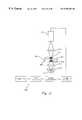
- FIG. 1Shown in FIG. 1 is a molecule detection system 10 for testing a sample for the presence of target molecules, in accordance with a preferred embodiment of the present invention.
- a source system 12having a photon source 13 , provides electromagnetic radiation directed to a molecular probe array 14 .
- Array 14typically comprises a plurality of test sites 15 formed into a substrate 16 .
- Test sites 15contain probe molecules that can bind to target molecules suspected of being present in the sample.
- An active pixel sensor 18detects electromagnetic radiation from array 14 .
- the electromagnetic radiation emitted from source system 12 and array 14is preferably in the infrared, visible, or ultra-violet.
- a source optical system 20focuses the electromagnetic radiation from source system 12 onto array 14
- a detector optical system 22focuses electromagnetic radiation emitted from array 14 onto active pixel sensor 18
- Source system 12may be provided with source filters 23 and 24 to filter the electromagnetic radiation from source 13
- a detector filter 26may be provided to filter the electromagnetic radiation emitted from array 14
- Driving electronics 28are provided to control active pixel sensor 18 .
- a data interface 30is also provided to allow control of system 10 by a computer 32 and to allow for data transfer to and from computer 32 .
- driving electronics 28may be provided with a microprocessor (not shown) to control system 10 , thereby obviating the need for computer 32 .
- a power source 34provides the electrical power needed to operate source 13 , active pixel sensor 18 , driving electronics 28 , and data interface 30 .
- Power source 34is preferably a battery and may be as simple as a single 9-volt battery.
- System 10is preferably provided as a portable system, and this is made possible by the use of active pixel sensor 18 .
- source 13produces electromagnetic radiation in only a narrow range of wavelengths and is easily portable.
- source 13could be a laser, such as a diode laser, or source 13 could be a light-emitting diode or an organic electro-luminescent device.
- Such sourcestypically produce electromagnetic radiation in only a single narrow wavelength range.
- source system 12may also be configured to provide electromagnetic radiation in a plurality of wavelength ranges, preferably narrow wavelength ranges.
- source 13can be a broadband source, such as an arc lamp, in which case filters 23 and 24 may be used to select the desired range of wavelengths to be directed to array 14 .
- source system 12is shown in FIG. 1 with only two filters 23 and 24 for purposes of illustration, source system 12 may include a greater or fewer number of filters.
- Source system 12 ′capable of providing electromagnetic radiation in a plurality of wavelength ranges is shown in FIG. 2 .
- Source system 12 ′includes photon sources 36 and 38 that are preferably lasers. Sources 36 and 38 may be chosen such that they produce electromagnetic radiation in different wavelength ranges, so that by selecting the output from either source 36 or source 38 , source system 12 ′ is able to provide radiation in two different wavelength ranges. Additionally, although only two sources 36 and 38 are shown in FIG. 2, source system 12 ′ may include a greater number. In general, source system 12 ′ may be provided with a separate source for each wavelength range.
- Non-linear optical elementsA more compact arrangement, however, may be provided by the use of non-linear optical elements.
- the output of source 38is directed to a non-linear optical element 40
- the output of source 36is directed to non-linear optical element 40 via a mirror 42 .
- Non-linear optical element 40combines the wavelengths from sources 36 and 38 to produce electromagnetic radiation having a shorter wavelength.
- a filter 44may then be used to selectively pass this shorter wavelength radiation.
- a single non-linear optical element 40is shown in FIG. 2 for purposes of illustration, a greater number maybe included in source system 12 ′.
- the non-linear optical elements in source system 12 ′may combine wavelengths from more than one source, or they may change the wavelength from a single source.
- source system 12 ′can be configured to provide electromagnetic radiation in a plurality of desired wavelength ranges.
- a first array embodiment 50comprises a plurality of wells formed into a glass slide 52 .
- array 50is shown in FIG. 3 with only four wells, namely wells 54 - 60 , though array 50 can include a greater or fewer number of wells.
- Wells 54 - 60may be formed into glass slide by conventional etching techniques.
- Disposed in wells 54 - 60are corresponding gel portions 62 - 68 .
- the gelis preferably a polyacrylamide gel.
- Probe moleculesare disposed in gel portions 62 - 68 , as described below in more detail. Alternatively, the probe molecules may be attached to the surfaces of wells 54 - 60 , such as by using epoxysilane chemistry, instead of being suspended in gel.
- a second array embodiment 70comprises a substantially flat substrate 72 , such as a glass slide, on which are disposed islands of gel 74 - 80 .
- the gelis preferably a polyacrylamide gel.
- Probe moleculesare disposed gel islands 74 - 80 , as described below in more detail.
- array 70is shown in FIG. 4 with only four gel islands 74 - 80 , though array 70 can include a greater or fewer number of gel islands.
- a third array embodiment 100comprises a glass slide 102 coated with a gel layer 104 .
- Gel layer 104preferably comprises a polyacrylamide gel.
- Gel layer 104is provided with a plurality of test sites.
- array 100is shown in FIG. 5 with only four test sites, namely sites 106 - 112 , though a greater or fewer number of test sites may also be provided.
- Each test site 106 - 112is defined by the region where added probe molecules have diffused into gel layer 104 .
- Probe moleculesmay be added to gel layer 104 by any means suitable for adding small amounts of material, such as micropipetting.
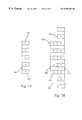
- Active pixel sensor 18comprises a plurality of pixel cells formed into a substrate 120 .
- active pixel sensor 18is shown in FIG. 5 with only four pixel cells 122 - 128 , though active pixel sensor 18 will typically have a far greater number.
- Each of pixel cells 122 - 128typically includes a photogate (not shown), a charge transfer section (not shown), and a readout circuit (not shown).
- An example of a suitable active pixel sensoris the SCM20014, sold by Motorola, Inc.
- the data sheets for the SCM20014(Aug. 9, 1999 version) are fully incorporated herein by reference.
- the SCM20014is beneficially provided with correlated double sampling and frame rate clamping to reduce fixed pattern noise.
- the SCM20014is also provided with electronic shuttering, whereby the exposure time of the pixels can be controlled electronically. This eliminates the need for an external shutter, thereby further simplifying system 10 .
- SCM20014is run in digital mode in order to take advantage of its digital signal processing capabilities, such as data companding.
- detector optical system 22preferably focuses each test site in array 14 onto one or more pixel cells of active pixel sensor 18 .
- each of test sites 106 - 112may be focused onto a corresponding one of pixel cells 122 - 128 .
- pixel cells 122 - 128are preferably provided with microlenses 130 - 136 , respectively.
- the best sensitivityis typically achieved by imaging each test site onto only a single pixel of active pixel sensor 18 .
- each test sitemay instead be focused onto a plurality of pixels of active pixel sensor 18 .
- substrate 16 of array 14may be attached directly to active pixel sensor 18 .
- active pixel sensor 18may be fabricated with a SiO 2 layer on top of the pixels. Either a layer of gel or islands of gel may then be placed on top of this SiO 2 layer.
- substrate 16 of array 14may be built out of glass on top of this SiO 2 layer.
- Each of pixel cells 122 - 128is also preferably provided with a color filter 138 - 144 , respectively.
- Each of color filters 138 - 144is designed to allow only a certain desired range of wavelengths to pass to pixel cell 122 - 128 for detection, as described in more detail below.
- Each of color filters 138 - 144can comprise a layer of polyimide resin that has been dyed to provide the desired wavelength response.
- Color filters 138 - 144can each have the same or different wavelength responses.
- Probe molecules of known typeare added to test sites 15 in array 14 , such as by micropipetting.
- the probe moleculesare chosen so as to be able to bind with the target molecules that are suspected of being present in the sample to form bound complexes. Accordingly, what probe molecules are used will depend on what target molecules are to be detected.
- the probe moleculesare preferably the corresponding antibody.
- the probe moleculesare preferably the corresponding antigen.
- the probe moleculesshould have nucleotide sequences that are complementary to at least a portion of the nucleotide sequence that the nucleic acids may have. Other types of target molecules may also be detected by using appropriate probe molecules that are able to bind with them.
- the probe molecules added to test sites 15may all be of the same type. Alternatively, different types of probe molecules may be added to different test sites. In this way, different certain test sites can be made sensitive to different types of target molecules and can be used to characterize the nature of the target molecules present in the sample.
- the probe molecules present in test sites 106 - 112may be oligonucleotides, each having a different nucleotide sequence.
- bindingwere to occur in only site 110 , then it could be determined that the nucleic acids in the sample had the nucleotide sequence complementary to site 110 but lacked the nucleotide sequence complementary to sites 106 , 108 , and 112 .
- bindingwere to occur in all of sites 106 - 112 , and the sample included only one type of nucleic acid, then one could infer that the target nucleic acid included nucleotide sequences complementary to the nucleotide sequences of all of sites 106 - 112 .
- test sites 15After the probe molecules are disposed in test sites 15 , the sample is then added to test sites 15 . For example, portions of the sample may be micropipetted onto each of test sites 15 . Alternatively, test sites 15 may be immersed in the sample. However, other means of exposure could also be used. After the sample is allowed to bind with the probe molecules in test sites 15 , array 14 is preferably rinsed to remove unreacted sample.
- the target molecules in the samplemay be conjugated to a fluorophore before they are exposed to the probe molecules.
- Many molecules of biological interestsuch as proteins and nucleic acids, can be conjugated to fluorophores using well-known techniques. Table 1 lists some examples of suitable fluorophores, but many others could also be used.
- optical detectionmay also facilitated by exposing the bound complexes in test sites 15 to a selective dye, such as ethidium bromide, as described above, or to fluorescent reporter molecules, as described in more detail below. Bound complexes in test sites 15 can also be made luminescent in other ways so as to facilitate optical detection.
- the bound complexes in test sites 15could also be phosphorescent, chemiluminescent, bioluminescent, electro-luminescent, or electro-chemiluminescent.
- the bound complexesmay not be luminescent at all. Instead, binding may be detected by measuring the absorbance of the bound complexes at a given wavelength.
- array 14is exposed to incident electromagnetic radiation from source system 12 .
- the wavelength used for the incident radiationwill depend on a number of factors. If the target molecules have been conjugated to a fluorophore, then the wavelength of the incident radiation is chosen to correspond to the excitation wavelength of the fluorophore. Table 1 lists the excitation wavelengths typically used for a number of different fluorophores. If a selective dye, such as ethidium bromide, is also intercalated into the bound complexes, then the wavelength of the incident radiation is preferably chosen to be the excitation wavelength of the selective dye.
- the wavelengthis chosen to be the excitation wavelength for the reporter molecules. If the bound complexes are phosphorescent, then the wavelength is chosen so as to induce the phosphorescence. If the bound complexes are not luminescent at all, then the wavelength of the incident radiation is preferably chosen so that the bound complexes will have a substantially different absorbance than unbound probe molecules.
- Active pixel sensor 18is then used to detect the electromagnetic radiation emitted from array 14 . If the bound complexes are fluorescent or have been made fluorescent by exposure to selective dyes or fluorescent reporter molecules, then detection occurs during illumination from source system 12 , and the emitted radiation of interest will be the fluorescence radiation emitted by that fluorophore. Table 1 lists the range of wavelengths characteristically emitted by a number of different fluorophores.
- the pixels of sensor 18are preferably provided with filters, such as filters 138 - 144 described above, that block the wavelength of the incident radiation and pass the wavelengths characteristic for the fluorescence radiation, so that the pixels will detect primarily the fluorescence radiation, rather than the incident radiation.
- active pixel sensor 18may be oriented at an angle such that neither the incident radiation passing through array 14 nor the incident radiation specularly reflected from array 14 fall on active pixel sensor 18 .
- source system 12 and active pixel sensor 18may be located on the same side of array 14 .
- a wavelength-dependent beam splitter(not shown) may be placed in the path of the incident radiation between source system 12 and array 14 that preferentially directs the fluorescence radiation toward active pixel sensor 18 . Binding is then detected by the presence of fluorescence radiation, i.e., by detecting an increase in the detected light level, as compared to a control.
- the controlcould be, for example, the light level detected before binding.
- the absorbance of the bound complexesis to be measured, then filters to block the incident radiation are not necessary. Instead, the test sites with bound complexes are detected by an increase in absorbance of the incident radiation, i.e., a decrease in the detected light level as compared to a control.
- the controlcould be, for example, the light level detected before binding.
- active pixel sensor 18detects the electromagnetic radiation emitted from test sites 15 only after the illumination from source system 12 ceases. Accordingly, active pixel sensor 18 is preferably provided with an electronic shuttering capability. Specifically, source system 12 illuminates test sites 15 while active pixel sensor 18 is electronically shuttered to allow bound complexes to absorb the incident radiation. Then, source system 12 is turned off or blocked, and active pixel 18 is enabled to detect phosphorescence from the bound complexes in test sites 15 . Notably, because the incident radiation is not present during detection filters between active pixel sensor 18 and array 14 are not necessary.
- the bound complexesare chemiluminescent, bioluminescent, electro-luminescent, or electro-chemiluminescent, then source system 12 is not needed. Instead, the luminescence from the bound complexes in test sites 15 is simply detected by active pixel sensor 18 .
- probe molecules disposed in a gelsuch as in array 50 , 70 , or 100 .
- fluorescence radiation emitted from the bound complexes in the test sitescan be made more spatially concentrated.
- the bound complexeswill be arranged in a three-dimensional pattern in the gel.
- the resulting bound complexeswill be more spread out, and the intensity of the resulting signal will be reduced. Accordingly, the binding of probe molecules is more easily detected when the probe molecules are disposed in a gel rather than when they are attached to a surface.
- An embodiment of system 10can also be used for “multi-color” tests.
- multi-color testsmultiple fluorophores are used, with each fluorophore emitting fluorescence radiation in a distinct range of wavelengths.
- Multiple filtersare used so that active pixel sensor 18 detects the fluorescence radiation from only one fluorophore at a time.
- the multiple filtersare preferably integral to active pixel sensor 18 , such as filters 138 - 144 shown in FIG. 6 .
- filter 26can be changed to detect each fluorophore.
- Single-base extension testscomprise an important class of multi-color test. Single-base extension tests may be used to identify unknown nucleotides in nucleic acids present in a sample.
- An example of a 3′ offset single-base extension testis illustrated in FIGS. 7A-C. Shown in FIG. 7A is a probe molecule 200 comprising a sequence of five nucleotides and having a 3′ end 202 and a 5′ end 204 . Probe molecule 200 is disposed in a given test site, such as site 106 in FIG. 5 . Shown in FIG. 7B is a bound complex 210 formed after a sample containing a target nucleic acid 212 has been added to site 106 .
- probe molecule 200contains a nucleotide sequence that is complementary to a nucleotide sequence present in target nucleic acid 212 .
- target nucleic acid 212has an unknown nucleotide 214 adjacent the nucleotide of nucleic acid 212 that hybridized with the nucleotide at 3′ prime end 202 of probe molecule 200 . If any unbound sample remains in test site 106 after binding is completed, it may be removed in a rinse step.
- reporter molecules 216 - 222comprises a single nucleotide base conjugated to a distinct fluorophore.
- reporter 216may comprise adenine conjugated to ALEXA FLUOR 350; reporter 218 may comprise cytosine conjugated to ALEXA FLUOR 532; reporter 210 may comprise guanine conjugated to ALEXA FLUOR 568; and reporter 212 may comprise thymine conjugated to BODIPY 650.
- the identity of unknown nucleotide 214will determine which of reporters 216 - 222 will bind to it.
- any remaining reporter molecules 216 - 222are removed by rinsing site 106 .
- Site 106 in array 14is then exposed to radiation from source system 12 at the various wavelengths required to cause fluorescence in reporters 216 - 222 in succession.
- array 14would be exposed successively to incident radiation at wavelengths 346 nm (for reporter 216 ), 531 nm (for reporter 218 ), 578 nm (for reporter 220 ), and 643 nm (for reporter 222 ).
- test site 106is imaged, such as by using optical system 22 , onto at least four pixels of active pixel sensor 18 , such as pixels 122 - 128 shown in FIG. 6 .
- each of filters 138 - 144 on pixels 122 - 128is designed to pass the fluorescence radiation of one of the four fluorophores while blocking the excitation wavelength used for that fluorophore.
- pixels 122 - 128serve to detect fluorescence radiation from reporters 216 - 222 , respectively.
- the identity of unknown nucleotide 214can then be determined based on whichever of pixels 122 - 128 detects a substantial increase in fluorescence radiation, as compared to a control.
- the controlmay, for example, be the amount of radiation detected by the pixel before reporter molecules 216 - 222 were added.
- reporter 220comprising guanine
- nucleotide 214must be cytosine.
- the 3′ inclusive single-base extension testis an alternative way to identify an unknown nucleotide in a nucleic acid.
- Four different probe molecules 300 - 306are disposed in four different test sites, such as test sites 106 - 112 in FIG. 5 .
- Probe molecules 300 - 306are distinguished from each other by the nucleotide present at the 3′ end. In particular, at the 3′ end, probe 300 has a guanine nucleotide, probe 302 has a cytosine nucleotide, probe 304 has an adenine nucleotide, and probe 306 has a thymine nucleotide.
- Probe molecules 300 - 306 disposed in test sites 106 - 112are then exposed to a sample containing nucleic acid 210 .
- Nucleic acid 210has an unknown nucleotide 214 (which is actually cytosine), and a known nucleotide 316 (e.g., thymine) adjacent to unknown nucleotide 214 .
- Nucleic acid 210is able to hybridize with each of probes 300 - 306 , to form bound complexes 320 - 326 , respectively.
- nucleotide 214is actually cytosine
- nucleotide 214is hybridized with the nucleotide at the 3′ end of the probe molecule only in bound complex 320 .
- This hybridization of unknown nucleotide 214may then be detected by exposing bound complexes 320 - 326 to a reporter 330 , comprising an adenine nucleotide conjugated to a fluorophore, as reporter 330 will hybridize only with bound complex 320 . After reporter molecules 330 are given sufficient time to bind to bound complexes 320 - 326 , any excess may be rinsed away.
- Array 14is exposed to electromagnetic radiation from source at the fluorophore's excitation wavelength.
- Test sites 106 - 112are imaged onto pixels 122 - 128 , respectively, and either integral filters 138 - 144 or detector filter 26 are provided to block the excitation wavelength and pass the fluorescence radiation. In this way, the identity of unknown nucleotide 214 may be determined based on which of pixels 122 - 128 detect fluorescence radiation.
- Active pixel sensor 18 in system 10can be also used for time-resolved studies.
- one or more pixels of active pixel sensor 18measure the electromagnetic radiation from one or more of test sites 15 of array 14 at successive time intervals.
- the population of specified molecules in test sites 15can be monitored as a function of time.
- the binding of probe molecules with target molecules to form bound complexes in test sites 15can be monitored as a function of time by active pixel sensor 18 monitoring the optical properties of test sites 15 . In this way, it can be determined when the binding process is complete.
- the optical properties measured by active pixel sensor 18can be the absorbance of test sites 15 of incident electromagnetic radiation of a given wavelength from source system 12 , as described above.
- the bound complexes in test sites 15may be luminescent, either fluorescent, phosphorescent, chemiluminescent, bioluminescent, electro-luminescent, or electro-chemiluminescent, in which case active pixel sensor 18 can monitor the population of bound complexes by detecting the luminescence from the bound complexes, as described above. To do time resolved studies, active pixel sensor 18 would simply take measurements at successive time intervals.
- FIG. 9Another important time-resolved application for active pixel sensor 18 is the monitoring of the population of nucleic acids amplified by processes such as the polymerase chain reaction (PCR).
- PCRpolymerase chain reaction
- FIG. 9shown in FIG. 9 is a molecule detection system 400 that includes an amplification device 402 .
- a nucleic acid amplification process, such as PCR,is conducted in an amplification chamber 404 formed in amplification device 402 .
- Amplification device 402is also provided with an input port 406 , connected to amplification chamber 404 , for adding the chemicals needed to perform PCR, and amplification device 402 is provided with an output port 408 , connected to amplification chamber 404 , for removal of the products.
- amplification device 402may be provided with optically transparent windows 410 and 412 at the top and bottom, respectively, of amplification chamber 402 .
- amplification device 402may itself be made out of an optically transparent material, such as glass.
- Active pixel sensor 18may monitor the population of amplified nucleic acids either by measuring the absorbance of incident electromagnetic radiation at a given wavelength passing through amplification chamber 404 or by measuring the fluorescence from the amplified nucleic acids in amplification chamber 404 .
- a source system 414which may be configured similarly to source systems 12 and 12 ′ described above, provides incident electromagnetic radiation directed to amplification chamber 404 , and active pixel sensor 18 detects the electromagnetic radiation from amplification chamber 404 through bottom window 412 .
- a source optical system 416may be used to focus the incident electromagnetic radiation from source system 414 into amplification chamber 404
- a detector optical system 418may be used to image selected areas in amplification chamber 404 onto active pixel sensor 18 .
- a detector filter 420preferably interposes amplification chamber 404 and active pixel sensor 18 to filter out the wavelengths corresponding to the incident radiation and pass the wavelengths corresponding to the fluorescence radiation.
- Detector filter 420may be integral to active pixel sensor 18 , as described above.
- active pixel sensor 18can take measurements at successive time intervals to monitor the progress of the amplification process.
- active pixel sensor 18may be used to detect the presence of specified molecules separated by processes such as capillary electrophoresis.
- a molecule detection system 500that includes a capillary electrophoresis device 502 .
- Capillary electrophoresis device 502is preferably a microfluidic device comprising a top layer 504 attached to a substrate layer 506 .
- Capillary electrophoresis channels 508 - 514are formed into substrate layer 506 . Though only four electrophoresis channels are shown for purposes of illustration, electrophoresis device 502 may include a greater or lesser number.
- layers 504 and 506are made out of an optically transparent material, such as glass or fused silica, to allow optical detection of the components separated in electrophoresis channels 508 - 514 .
- electrophoresis device 502may be provided with optically transparent windows (not shown).
- the specified moleculesmay be luminescent, most typically fluorescent, in which case they may be detected by their luminescence. Alternatively, the specified molecules may be detected by their absorbance.
- a source system 516provides incident electromagnetic radiation directed to electrophoresis device 502 .
- a source optical system 518preferably focuses the incident radiation into each of electrophoresis channels 508 - 514 .
- source optical system 516may include a cylindrical lens that focuses the incident radiation into a line cutting transversely across channels 508 - 514 .
- Active pixel sensor 18detects the electromagnetic radiation from specified locations in each of channels 508 - 514 .
- a detector optical system 520may be used to image the specified locations in channels 508 - 514 onto active pixel sensor 18 .
- different channelsare imaged onto different pixels of active pixel sensor 18 .
- channels 508 - 514may be imaged onto pixels 122 - 128 , respectively. In this way, channels 508 - 514 may be monitored simultaneously.
- a detector filter 522may be provided, and detector filter 522 may be integral to active pixel sensor 18 .
- Active pixel sensor 18takes measurements at successive time intervals during the electrophoretic separation process when the various chemical components added to device 502 migrate along channels 508 - 514 and become separated. In this way, system 500 can be used to determine when specified molecules pass the specified locations along channels 508 - 514 monitored by active pixel sensor 18 .
- active pixel sensor 18may be used to determine when specified molecules pass a given location in a flow cell.
- the specified moleculesmay be luminescent, such as fluorescent, or they my be detected by their absorbance at a given wavelength.
- FIG. 11Shown in FIG. 11 is a molecule detection system 600 including a flow cell 602 .
- Flow cell 602includes a channel 604 and optically transparent windows 606 and 608 .
- flow cell 602may be made out of an optically transparent material.
- An optical system 610focuses incident electromagnetic radiation from source system 612 to a given location 614 within channel 604 .
- a detector optical system 616images electromagnetic radiation from point 614 onto active pixel sensor 18 .
- a detector filter 618may also be provided, as shown in FIG.
- system 600can be used to detect when the specified molecules pass point 614 in flow cell 602 .
- the specified moleculesare fluorescent, the arrival of the specified molecules at location 614 would be detected by active pixel sensor 18 as an increase in the measured amount of fluorescence radiation. If the specified molecules are to be detected by their absorbance of the incident radiation, then the arrival of the specified molecules at location 614 would be detected by active pixel sensor 18 as a decrease in detected radiation.
- a devicesuch as a microfluidic device, may have more than one component monitored by an active pixel sensor.
- a microfluidic devicemay include a PCR chamber in one section and a capillary electrophoresis channel in another section, with each section being monitored by a separate active pixel sensor.
- the molecule detection systems of the present inventionmay, in general, include more than one active pixel sensor.
Landscapes
- Health & Medical Sciences (AREA)
- Nuclear Medicine, Radiotherapy & Molecular Imaging (AREA)
- Physics & Mathematics (AREA)
- Life Sciences & Earth Sciences (AREA)
- Chemical & Material Sciences (AREA)
- Analytical Chemistry (AREA)
- Biochemistry (AREA)
- General Health & Medical Sciences (AREA)
- General Physics & Mathematics (AREA)
- Immunology (AREA)
- Pathology (AREA)
- Investigating, Analyzing Materials By Fluorescence Or Luminescence (AREA)
Abstract
Description
| TABLE 1 | ||||
| Excitation | Fluorescence | |||
| Fluorescent Dye | Wavelength | Wavelength | ||
| Trade Name | (in nanometers) | (in nanometers) | ||
| ALEXA FLUOR 350 | 346 | 442 | ||
| ALEXA FLUOR 430 | 431 | 541 | ||
| ALEXA FLUOR 532 | 531 | 554 | ||
| ALEXA FLUOR 568 | 578 | 603 | ||
| BODIPY 650 | 643 | 666 | ||
Claims (27)
Priority Applications (6)
| Application Number | Priority Date | Filing Date | Title |
|---|---|---|---|
| US09/440,031US6596483B1 (en) | 1999-11-12 | 1999-11-12 | System and method for detecting molecules using an active pixel sensor |
| EP00978529AEP1228356A1 (en) | 1999-11-12 | 2000-11-10 | System and method for detecting molecules using an active pixel sensor |
| CA002391119ACA2391119A1 (en) | 1999-11-12 | 2000-11-10 | System and method for detecting molecules using an active pixel sensor |
| AU15985/01AAU775888B2 (en) | 1999-11-12 | 2000-11-10 | System and method for detecting molecules using an active pixel sensor |
| PCT/US2000/031031WO2001035080A1 (en) | 1999-11-12 | 2000-11-10 | System and method for detecting molecules using an active pixel sensor |
| US10/436,969US20040096854A1 (en) | 1999-11-12 | 2003-05-12 | System and method for detecting molecules using an active pixel sensor |
Applications Claiming Priority (1)
| Application Number | Priority Date | Filing Date | Title |
|---|---|---|---|
| US09/440,031US6596483B1 (en) | 1999-11-12 | 1999-11-12 | System and method for detecting molecules using an active pixel sensor |
Related Child Applications (1)
| Application Number | Title | Priority Date | Filing Date |
|---|---|---|---|
| US10/436,969DivisionUS20040096854A1 (en) | 1999-11-12 | 2003-05-12 | System and method for detecting molecules using an active pixel sensor |
Publications (1)
| Publication Number | Publication Date |
|---|---|
| US6596483B1true US6596483B1 (en) | 2003-07-22 |
Family
ID=23747137
Family Applications (2)
| Application Number | Title | Priority Date | Filing Date |
|---|---|---|---|
| US09/440,031Expired - LifetimeUS6596483B1 (en) | 1999-11-12 | 1999-11-12 | System and method for detecting molecules using an active pixel sensor |
| US10/436,969AbandonedUS20040096854A1 (en) | 1999-11-12 | 2003-05-12 | System and method for detecting molecules using an active pixel sensor |
Family Applications After (1)
| Application Number | Title | Priority Date | Filing Date |
|---|---|---|---|
| US10/436,969AbandonedUS20040096854A1 (en) | 1999-11-12 | 2003-05-12 | System and method for detecting molecules using an active pixel sensor |
Country Status (5)
| Country | Link |
|---|---|
| US (2) | US6596483B1 (en) |
| EP (1) | EP1228356A1 (en) |
| AU (1) | AU775888B2 (en) |
| CA (1) | CA2391119A1 (en) |
| WO (1) | WO2001035080A1 (en) |
Cited By (33)
| Publication number | Priority date | Publication date | Assignee | Title |
|---|---|---|---|---|
| US20040027872A1 (en)* | 2001-04-12 | 2004-02-12 | Fuji Electric Co., Ltd. | Semiconductor physical quantity sensing device |
| US6969835B1 (en)* | 1999-06-29 | 2005-11-29 | Packard Instrument Company Inc. | Imaging assay analysis for microsamples |
| DE102004056735A1 (en)* | 2004-11-09 | 2006-07-20 | Clondiag Chip Technologies Gmbh | Device for performing and analyzing microarray experiments |
| US20060256350A1 (en)* | 2005-02-01 | 2006-11-16 | David Nolte | Laser scanning interferometric surface metrology |
| US20070003925A1 (en)* | 2005-02-01 | 2007-01-04 | Nolte David D | Multiplexed biological analyzer planar array apparatus and methods |
| US20070259366A1 (en)* | 2006-05-03 | 2007-11-08 | Greg Lawrence | Direct printing of patterned hydrophobic wells |
| US20080186477A1 (en)* | 2007-01-19 | 2008-08-07 | Xuefeng Wang | System with extended range of molecular sensing through integrated multi-modal data acquisition |
| US20080230605A1 (en)* | 2006-11-30 | 2008-09-25 | Brian Weichel | Process and apparatus for maintaining data integrity |
| US20080304073A1 (en)* | 2007-03-26 | 2008-12-11 | Nolte David D | Method and apparatus for conjugate quadrature interferometric detection of an immunoassay |
| US7522282B2 (en) | 2006-11-30 | 2009-04-21 | Purdue Research Foundation | Molecular interferometric imaging process and apparatus |
| US20110236901A1 (en)* | 2008-12-05 | 2011-09-29 | Aleksey Kolesnychenko | Thermal cycling system comprising transport heater |
| US20120200749A1 (en)* | 2011-02-03 | 2012-08-09 | Ulrich Boettiger | Imagers with structures for near field imaging |
| US8298831B2 (en) | 2005-02-01 | 2012-10-30 | Purdue Research Foundation | Differentially encoded biological analyzer planar array apparatus and methods |
| US8494501B2 (en) | 2000-12-19 | 2013-07-23 | At&T Intellectual Property I, L.P. | Identity blocking service from a wireless service provider |
| US8639235B2 (en) | 2000-12-19 | 2014-01-28 | At&T Intellectual Property I, L.P. | System and method for using location information to execute an action |
| US8644506B2 (en) | 2000-12-19 | 2014-02-04 | At&T Intellectual Property I, L.P. | Location-based security rules |
| WO2014066704A1 (en) | 2012-10-24 | 2014-05-01 | Genmark Diagnostics, Inc. | Integrated multiplex target analysis |
| US8874140B2 (en) | 2000-12-19 | 2014-10-28 | At&T Intellectual Property I, L.P. | Location blocking service from a wireless service provider |
| US20150177150A1 (en)* | 2013-11-17 | 2015-06-25 | Quantum-Si Incorporated | Optical system and assay chip for probing, detecting and analyzing molecules |
| US9146248B2 (en) | 2013-03-14 | 2015-09-29 | Intelligent Bio-Systems, Inc. | Apparatus and methods for purging flow cells in nucleic acid sequencing instruments |
| US9222623B2 (en) | 2013-03-15 | 2015-12-29 | Genmark Diagnostics, Inc. | Devices and methods for manipulating deformable fluid vessels |
| WO2016077364A2 (en) | 2014-11-11 | 2016-05-19 | Genmark Diagnostics, Inc. | Instrument and cartridge for performing assays in a closed sample preparation and reaction system |
| WO2016077341A2 (en) | 2014-11-11 | 2016-05-19 | Genmark Diagnostics, Inc. | Instrument and cartridge for performing assays in a closed sample preparation and reaction system employing electrowetting fluid manipulation |
| US9501780B2 (en) | 2000-12-19 | 2016-11-22 | At&T Intellectual Property I, L.P. | Surveying wireless device users by location |
| US9498778B2 (en) | 2014-11-11 | 2016-11-22 | Genmark Diagnostics, Inc. | Instrument for processing cartridge for performing assays in a closed sample preparation and reaction system |
| US9591268B2 (en) | 2013-03-15 | 2017-03-07 | Qiagen Waltham, Inc. | Flow cell alignment methods and systems |
| US9598722B2 (en) | 2014-11-11 | 2017-03-21 | Genmark Diagnostics, Inc. | Cartridge for performing assays in a closed sample preparation and reaction system |
| WO2018053501A1 (en) | 2016-09-19 | 2018-03-22 | Genmark Diagnostics, Inc. | Instrument for processing cartridge for performing assays in a closed sample preparation and reaction system |
| US10106847B1 (en) | 2017-08-24 | 2018-10-23 | Clinical Micro Sensors, Inc. | Electrochemical detection of bacterial and/or fungal infections |
| WO2019040769A1 (en) | 2017-08-24 | 2019-02-28 | Clinical Micro Sensors, Inc. (dba GenMark Diagnostics, Inc.) | Electrochemical detection of bacterial and/or fungal infections |
| US10495656B2 (en) | 2012-10-24 | 2019-12-03 | Genmark Diagnostics, Inc. | Integrated multiplex target analysis |
| USD881409S1 (en) | 2013-10-24 | 2020-04-14 | Genmark Diagnostics, Inc. | Biochip cartridge |
| CN111272715A (en)* | 2018-12-04 | 2020-06-12 | 长光华大基因测序设备(长春)有限公司 | Fluorescence imaging system of gene sequencer |
Families Citing this family (13)
| Publication number | Priority date | Publication date | Assignee | Title |
|---|---|---|---|---|
| EP1345026B1 (en) | 2002-03-15 | 2010-05-05 | Affymetrix, Inc. | System and method for scanning of biological materials |
| US7317415B2 (en) | 2003-08-08 | 2008-01-08 | Affymetrix, Inc. | System, method, and product for scanning of biological materials employing dual analog integrators |
| US20050221351A1 (en)* | 2004-04-06 | 2005-10-06 | Affymetrix, Inc. | Methods and devices for microarray image analysis |
| US9445025B2 (en) | 2006-01-27 | 2016-09-13 | Affymetrix, Inc. | System, method, and product for imaging probe arrays with small feature sizes |
| US8055098B2 (en) | 2006-01-27 | 2011-11-08 | Affymetrix, Inc. | System, method, and product for imaging probe arrays with small feature sizes |
| US8009889B2 (en) | 2006-06-27 | 2011-08-30 | Affymetrix, Inc. | Feature intensity reconstruction of biological probe array |
| US7629124B2 (en)* | 2006-06-30 | 2009-12-08 | Canon U.S. Life Sciences, Inc. | Real-time PCR in micro-channels |
| US7803609B2 (en) | 2006-07-21 | 2010-09-28 | Affymetrix, Inc. | System, method, and product for generating patterned illumination |
| JP5026851B2 (en)* | 2007-04-23 | 2012-09-19 | 株式会社日立製作所 | Chemiluminescence detector |
| US9767342B2 (en) | 2009-05-22 | 2017-09-19 | Affymetrix, Inc. | Methods and devices for reading microarrays |
| US9408696B2 (en)* | 2013-09-29 | 2016-08-09 | Coloplast A/S | Method of treating peyronie's disease |
| MX2019010854A (en)* | 2017-03-13 | 2019-10-30 | Zoetis Services Llc | SIDE FLOW TEST SYSTEM. |
| US20210187503A1 (en)* | 2019-12-19 | 2021-06-24 | Personal Genomics Taiwan, Inc. | Apparatus and system for single-molecule nucleic acids detection |
Citations (21)
| Publication number | Priority date | Publication date | Assignee | Title |
|---|---|---|---|---|
| US4851331A (en) | 1986-05-16 | 1989-07-25 | Allied Corporation | Method and kit for polynucleotide assay including primer-dependant DNA polymerase |
| WO1995000669A1 (en) | 1993-06-22 | 1995-01-05 | Pharmacia Biotech Ab | Parallel primer extension approach to nucleic acid sequence analysis |
| US5471515A (en) | 1994-01-28 | 1995-11-28 | California Institute Of Technology | Active pixel sensor with intra-pixel charge transfer |
| GB2289979A (en) | 1994-06-01 | 1995-12-06 | Simage Oy | Imaging devices systems and methods |
| US5585639A (en) | 1995-07-27 | 1996-12-17 | Hewlett-Packard Company | Optical scanning apparatus |
| US5653939A (en) | 1991-11-19 | 1997-08-05 | Massachusetts Institute Of Technology | Optical and electrical methods and apparatus for molecule detection |
| US5741411A (en)* | 1995-05-19 | 1998-04-21 | Iowa State University Research Foundation | Multiplexed capillary electrophoresis system |
| US5841126A (en) | 1994-01-28 | 1998-11-24 | California Institute Of Technology | CMOS active pixel sensor type imaging system on a chip |
| US5851772A (en)* | 1996-01-29 | 1998-12-22 | University Of Chicago | Microchip method for the enrichment of specific DNA sequences |
| US5863504A (en) | 1995-03-16 | 1999-01-26 | Bio-Rad Laboratories, Inc. | Fluorescence imaging instrument utilizing fish |
| US5874219A (en) | 1995-06-07 | 1999-02-23 | Affymetrix, Inc. | Methods for concurrently processing multiple biological chip assays |
| WO1999013109A1 (en) | 1997-09-11 | 1999-03-18 | Seq, Ltd. | Method for dna sequencing analysis |
| US5888819A (en) | 1991-03-05 | 1999-03-30 | Molecular Tool, Inc. | Method for determining nucleotide identity through primer extension |
| JPH11183437A (en) | 1997-12-22 | 1999-07-09 | Shimadzu Corp | Electrophoresis member and electrophoresis apparatus using the same |
| US5922617A (en) | 1997-11-12 | 1999-07-13 | Functional Genetics, Inc. | Rapid screening assay methods and devices |
| US5932873A (en)* | 1996-08-13 | 1999-08-03 | Foveon, Inc. | Capacitor-coupled bipolar active pixel sensor with integrated electronic shutter |
| US5945722A (en) | 1997-05-02 | 1999-08-31 | National Semiconductor Corporation | Color active pixel sensor cell with oxide color filter |
| US5981956A (en) | 1996-05-16 | 1999-11-09 | Affymetrix, Inc. | Systems and methods for detection of labeled materials |
| WO1999057547A2 (en) | 1998-05-05 | 1999-11-11 | The Perkin-Elmer Corporation | Method and system for velocity-normalized position-based scanning |
| US5991030A (en) | 1997-09-11 | 1999-11-23 | Hitachi Software Engineering Co., Ltd. | Apparatus for reading a luminescence pattern of a sample |
| US6325977B1 (en)* | 2000-01-18 | 2001-12-04 | Agilent Technologies, Inc. | Optical detection system for the detection of organic molecules |
Family Cites Families (2)
| Publication number | Priority date | Publication date | Assignee | Title |
|---|---|---|---|---|
| US5578832A (en)* | 1994-09-02 | 1996-11-26 | Affymetrix, Inc. | Method and apparatus for imaging a sample on a device |
| GB2289779B (en)* | 1994-05-24 | 1999-04-28 | Intel Corp | Method and apparatus for automatically scrubbing ECC errors in memory via hardware |
- 1999
- 1999-11-12USUS09/440,031patent/US6596483B1/ennot_activeExpired - Lifetime
- 2000
- 2000-11-10CACA002391119Apatent/CA2391119A1/ennot_activeAbandoned
- 2000-11-10WOPCT/US2000/031031patent/WO2001035080A1/ennot_activeApplication Discontinuation
- 2000-11-10AUAU15985/01Apatent/AU775888B2/ennot_activeCeased
- 2000-11-10EPEP00978529Apatent/EP1228356A1/ennot_activeWithdrawn
- 2003
- 2003-05-12USUS10/436,969patent/US20040096854A1/ennot_activeAbandoned
Patent Citations (23)
| Publication number | Priority date | Publication date | Assignee | Title |
|---|---|---|---|---|
| US4851331A (en) | 1986-05-16 | 1989-07-25 | Allied Corporation | Method and kit for polynucleotide assay including primer-dependant DNA polymerase |
| US5888819A (en) | 1991-03-05 | 1999-03-30 | Molecular Tool, Inc. | Method for determining nucleotide identity through primer extension |
| US5846708A (en) | 1991-11-19 | 1998-12-08 | Massachusetts Institiute Of Technology | Optical and electrical methods and apparatus for molecule detection |
| US5653939A (en) | 1991-11-19 | 1997-08-05 | Massachusetts Institute Of Technology | Optical and electrical methods and apparatus for molecule detection |
| WO1995000669A1 (en) | 1993-06-22 | 1995-01-05 | Pharmacia Biotech Ab | Parallel primer extension approach to nucleic acid sequence analysis |
| US5471515A (en) | 1994-01-28 | 1995-11-28 | California Institute Of Technology | Active pixel sensor with intra-pixel charge transfer |
| US5841126A (en) | 1994-01-28 | 1998-11-24 | California Institute Of Technology | CMOS active pixel sensor type imaging system on a chip |
| GB2289979A (en) | 1994-06-01 | 1995-12-06 | Simage Oy | Imaging devices systems and methods |
| US5863504A (en) | 1995-03-16 | 1999-01-26 | Bio-Rad Laboratories, Inc. | Fluorescence imaging instrument utilizing fish |
| US5885531A (en) | 1995-03-16 | 1999-03-23 | Bio-Rad Laboratories, Inc. | Fluorescence imaging instrument utilizing fish |
| US5741411A (en)* | 1995-05-19 | 1998-04-21 | Iowa State University Research Foundation | Multiplexed capillary electrophoresis system |
| US5874219A (en) | 1995-06-07 | 1999-02-23 | Affymetrix, Inc. | Methods for concurrently processing multiple biological chip assays |
| US5585639A (en) | 1995-07-27 | 1996-12-17 | Hewlett-Packard Company | Optical scanning apparatus |
| US5851772A (en)* | 1996-01-29 | 1998-12-22 | University Of Chicago | Microchip method for the enrichment of specific DNA sequences |
| US5981956A (en) | 1996-05-16 | 1999-11-09 | Affymetrix, Inc. | Systems and methods for detection of labeled materials |
| US5932873A (en)* | 1996-08-13 | 1999-08-03 | Foveon, Inc. | Capacitor-coupled bipolar active pixel sensor with integrated electronic shutter |
| US5945722A (en) | 1997-05-02 | 1999-08-31 | National Semiconductor Corporation | Color active pixel sensor cell with oxide color filter |
| WO1999013109A1 (en) | 1997-09-11 | 1999-03-18 | Seq, Ltd. | Method for dna sequencing analysis |
| US5991030A (en) | 1997-09-11 | 1999-11-23 | Hitachi Software Engineering Co., Ltd. | Apparatus for reading a luminescence pattern of a sample |
| US5922617A (en) | 1997-11-12 | 1999-07-13 | Functional Genetics, Inc. | Rapid screening assay methods and devices |
| JPH11183437A (en) | 1997-12-22 | 1999-07-09 | Shimadzu Corp | Electrophoresis member and electrophoresis apparatus using the same |
| WO1999057547A2 (en) | 1998-05-05 | 1999-11-11 | The Perkin-Elmer Corporation | Method and system for velocity-normalized position-based scanning |
| US6325977B1 (en)* | 2000-01-18 | 2001-12-04 | Agilent Technologies, Inc. | Optical detection system for the detection of organic molecules |
Non-Patent Citations (5)
| Title |
|---|
| Eric R. Fossum, "Novel Sensor Enables Low-Power, Miniaturized Imagers", Photonics Spectra, p. 125-126 (Jan., 1996). |
| Kheterpal, I., et al., DNA Sequencing using a Four-Color Confocal Fluorescence Capillary Array Scanner, Electrophoresis, 17: 1852-1859 (1996). |
| Motorola Inc., Motorola Semiconductor Technical Data for SCM200140 Image Sensor, dated Aug. 9, 1999. |
| NASA's Jet Propulsion Laboratory, "Active-Pixel-Sensor Digital Camera on a Single Chip", NASA Tech Briefs, p. 44-48 (Oct. 1998). |
| Orly Yadid-Pecht, Barmak Mansoorian, Eric R. Fossum and Bedabrata Pain, "Optimization of Noise and Responsivity in CMOS Active Pixel Sensors for Detection of Ultra Low Light Levels", Proceedings of SPIE, vol. 3019, p. 125-136 (Feb. 10-11, 1997). |
Cited By (72)
| Publication number | Priority date | Publication date | Assignee | Title |
|---|---|---|---|---|
| US6969835B1 (en)* | 1999-06-29 | 2005-11-29 | Packard Instrument Company Inc. | Imaging assay analysis for microsamples |
| US8639235B2 (en) | 2000-12-19 | 2014-01-28 | At&T Intellectual Property I, L.P. | System and method for using location information to execute an action |
| US8644506B2 (en) | 2000-12-19 | 2014-02-04 | At&T Intellectual Property I, L.P. | Location-based security rules |
| US8494501B2 (en) | 2000-12-19 | 2013-07-23 | At&T Intellectual Property I, L.P. | Identity blocking service from a wireless service provider |
| US8874140B2 (en) | 2000-12-19 | 2014-10-28 | At&T Intellectual Property I, L.P. | Location blocking service from a wireless service provider |
| US9020489B2 (en) | 2000-12-19 | 2015-04-28 | At&T Intellectual Property I, L.P. | System and method for using location information to execute an action |
| US9501780B2 (en) | 2000-12-19 | 2016-11-22 | At&T Intellectual Property I, L.P. | Surveying wireless device users by location |
| US10354079B2 (en) | 2000-12-19 | 2019-07-16 | Google Llc | Location-based security rules |
| US20040027872A1 (en)* | 2001-04-12 | 2004-02-12 | Fuji Electric Co., Ltd. | Semiconductor physical quantity sensing device |
| US7180798B2 (en)* | 2001-04-12 | 2007-02-20 | Fuji Electric Co., Ltd. | Semiconductor physical quantity sensing device |
| DE102004056735A1 (en)* | 2004-11-09 | 2006-07-20 | Clondiag Chip Technologies Gmbh | Device for performing and analyzing microarray experiments |
| US20070003925A1 (en)* | 2005-02-01 | 2007-01-04 | Nolte David D | Multiplexed biological analyzer planar array apparatus and methods |
| US7663092B2 (en) | 2005-02-01 | 2010-02-16 | Purdue Research Foundation | Method and apparatus for phase contrast quadrature interferometric detection of an immunoassay |
| US7405831B2 (en) | 2005-02-01 | 2008-07-29 | Purdue Research Foundation | Laser scanning interferometric surface metrology |
| US7910356B2 (en) | 2005-02-01 | 2011-03-22 | Purdue Research Foundation | Multiplexed biological analyzer planar array apparatus and methods |
| US20070003436A1 (en)* | 2005-02-01 | 2007-01-04 | Nolte David D | Method and apparatus for phase contrast quadrature interferometric detection of an immunoassay |
| US20060256350A1 (en)* | 2005-02-01 | 2006-11-16 | David Nolte | Laser scanning interferometric surface metrology |
| US8298831B2 (en) | 2005-02-01 | 2012-10-30 | Purdue Research Foundation | Differentially encoded biological analyzer planar array apparatus and methods |
| US20070259366A1 (en)* | 2006-05-03 | 2007-11-08 | Greg Lawrence | Direct printing of patterned hydrophobic wells |
| US7522282B2 (en) | 2006-11-30 | 2009-04-21 | Purdue Research Foundation | Molecular interferometric imaging process and apparatus |
| US20080230605A1 (en)* | 2006-11-30 | 2008-09-25 | Brian Weichel | Process and apparatus for maintaining data integrity |
| US8072585B2 (en) | 2007-01-19 | 2011-12-06 | Purdue Research Foundation | System with extended range of molecular sensing through integrated multi-modal data acquisition |
| US7659968B2 (en) | 2007-01-19 | 2010-02-09 | Purdue Research Foundation | System with extended range of molecular sensing through integrated multi-modal data acquisition |
| US20080186477A1 (en)* | 2007-01-19 | 2008-08-07 | Xuefeng Wang | System with extended range of molecular sensing through integrated multi-modal data acquisition |
| US7787126B2 (en) | 2007-03-26 | 2010-08-31 | Purdue Research Foundation | Method and apparatus for conjugate quadrature interferometric detection of an immunoassay |
| US20080304073A1 (en)* | 2007-03-26 | 2008-12-11 | Nolte David D | Method and apparatus for conjugate quadrature interferometric detection of an immunoassay |
| US10434514B2 (en)* | 2008-12-05 | 2019-10-08 | Biocartis S.A. | Thermal cycling system comprising transport heater |
| US20110236901A1 (en)* | 2008-12-05 | 2011-09-29 | Aleksey Kolesnychenko | Thermal cycling system comprising transport heater |
| US20120200749A1 (en)* | 2011-02-03 | 2012-08-09 | Ulrich Boettiger | Imagers with structures for near field imaging |
| WO2014066704A1 (en) | 2012-10-24 | 2014-05-01 | Genmark Diagnostics, Inc. | Integrated multiplex target analysis |
| EP2965817A1 (en) | 2012-10-24 | 2016-01-13 | Genmark Diagnostics Inc. | Integrated multiplex target analysis |
| USD900330S1 (en) | 2012-10-24 | 2020-10-27 | Genmark Diagnostics, Inc. | Instrument |
| US10495656B2 (en) | 2012-10-24 | 2019-12-03 | Genmark Diagnostics, Inc. | Integrated multiplex target analysis |
| EP3919174A2 (en) | 2012-10-24 | 2021-12-08 | Genmark Diagnostics Inc. | Integrated multiplex target analysis |
| US11952618B2 (en) | 2012-10-24 | 2024-04-09 | Roche Molecular Systems, Inc. | Integrated multiplex target analysis |
| US9957553B2 (en) | 2012-10-24 | 2018-05-01 | Genmark Diagnostics, Inc. | Integrated multiplex target analysis |
| EP3427830A1 (en) | 2012-10-24 | 2019-01-16 | Genmark Diagnostics Inc. | Integrated multiplex target analysis |
| US9146248B2 (en) | 2013-03-14 | 2015-09-29 | Intelligent Bio-Systems, Inc. | Apparatus and methods for purging flow cells in nucleic acid sequencing instruments |
| US9453613B2 (en) | 2013-03-15 | 2016-09-27 | Genmark Diagnostics, Inc. | Apparatus, devices, and methods for manipulating deformable fluid vessels |
| US9222623B2 (en) | 2013-03-15 | 2015-12-29 | Genmark Diagnostics, Inc. | Devices and methods for manipulating deformable fluid vessels |
| US10807090B2 (en) | 2013-03-15 | 2020-10-20 | Genmark Diagnostics, Inc. | Apparatus, devices, and methods for manipulating deformable fluid vessels |
| US9410663B2 (en) | 2013-03-15 | 2016-08-09 | Genmark Diagnostics, Inc. | Apparatus and methods for manipulating deformable fluid vessels |
| US9591268B2 (en) | 2013-03-15 | 2017-03-07 | Qiagen Waltham, Inc. | Flow cell alignment methods and systems |
| US10391489B2 (en) | 2013-03-15 | 2019-08-27 | Genmark Diagnostics, Inc. | Apparatus and methods for manipulating deformable fluid vessels |
| US10249038B2 (en) | 2013-03-15 | 2019-04-02 | Qiagen Sciences, Llc | Flow cell alignment methods and systems |
| USD881409S1 (en) | 2013-10-24 | 2020-04-14 | Genmark Diagnostics, Inc. | Biochip cartridge |
| US10533945B2 (en) | 2013-11-17 | 2020-01-14 | Quantum-Si Incorporated | Optical system and assay chip for probing, detecting and analyzing molecules |
| US12163888B2 (en) | 2013-11-17 | 2024-12-10 | Quantum-Si Incorporated | Optical system and assay chip for probing, detecting and analyzing molecules |
| US20150177150A1 (en)* | 2013-11-17 | 2015-06-25 | Quantum-Si Incorporated | Optical system and assay chip for probing, detecting and analyzing molecules |
| US11287382B2 (en) | 2013-11-17 | 2022-03-29 | Quantum-Si Incorporated | Optical system and assay chip for probing, detecting and analyzing molecules |
| KR20160108318A (en)* | 2013-11-17 | 2016-09-19 | 퀀텀-에스아이 인코포레이티드 | Optical system and assay chip for probing, detecting and analyzing molecules |
| KR102221637B1 (en) | 2013-11-17 | 2021-03-02 | 퀀텀-에스아이 인코포레이티드 | Optical system and assay chip for probing, detecting and analyzing molecules |
| US9863880B2 (en)* | 2013-11-17 | 2018-01-09 | Quantum-Si Incorporated | Optical system and assay chip for probing, detecting and analyzing molecules |
| US9598722B2 (en) | 2014-11-11 | 2017-03-21 | Genmark Diagnostics, Inc. | Cartridge for performing assays in a closed sample preparation and reaction system |
| EP3831481A1 (en) | 2014-11-11 | 2021-06-09 | Genmark Diagnostics Inc. | Instrument and cartridge for performing assays in a closed sample preparation and reaction system |
| EP4578539A2 (en) | 2014-11-11 | 2025-07-02 | Roche Diagnostics GmbH | Instrument and cartridge for performing assays in a closed sample preparation and reaction system |
| US9498778B2 (en) | 2014-11-11 | 2016-11-22 | Genmark Diagnostics, Inc. | Instrument for processing cartridge for performing assays in a closed sample preparation and reaction system |
| WO2016077341A2 (en) | 2014-11-11 | 2016-05-19 | Genmark Diagnostics, Inc. | Instrument and cartridge for performing assays in a closed sample preparation and reaction system employing electrowetting fluid manipulation |
| WO2016077364A2 (en) | 2014-11-11 | 2016-05-19 | Genmark Diagnostics, Inc. | Instrument and cartridge for performing assays in a closed sample preparation and reaction system |
| US10864522B2 (en) | 2014-11-11 | 2020-12-15 | Genmark Diagnostics, Inc. | Processing cartridge and method for detecting a pathogen in a sample |
| US10005080B2 (en) | 2014-11-11 | 2018-06-26 | Genmark Diagnostics, Inc. | Instrument and cartridge for performing assays in a closed sample preparation and reaction system employing electrowetting fluid manipulation |
| WO2018053501A1 (en) | 2016-09-19 | 2018-03-22 | Genmark Diagnostics, Inc. | Instrument for processing cartridge for performing assays in a closed sample preparation and reaction system |
| US11300578B2 (en) | 2016-09-19 | 2022-04-12 | Roche Molecular Systems, Inc. | Instrument for processing cartridge for performing assays in a closed sample preparation and reaction system |
| US12000847B2 (en) | 2016-09-19 | 2024-06-04 | Roche Molecular Systems, Inc. | Instrument for processing cartridge for performing assays in a closed sample preparation and reaction system |
| US11021759B2 (en) | 2017-08-24 | 2021-06-01 | Clinical Micro Sensors, Inc. | Electrochemical detection of bacterial and/or fungal infections |
| US10273535B2 (en) | 2017-08-24 | 2019-04-30 | Clinical Micro Sensors, Inc. | Electrochemical detection of bacterial and/or fungal infections |
| US10106847B1 (en) | 2017-08-24 | 2018-10-23 | Clinical Micro Sensors, Inc. | Electrochemical detection of bacterial and/or fungal infections |
| WO2019040769A1 (en) | 2017-08-24 | 2019-02-28 | Clinical Micro Sensors, Inc. (dba GenMark Diagnostics, Inc.) | Electrochemical detection of bacterial and/or fungal infections |
| EP4549590A2 (en) | 2017-08-24 | 2025-05-07 | Roche Diagnostics GmbH | Electrochemical detection of bacterial and/or fungal infections |
| US10669592B2 (en) | 2017-08-24 | 2020-06-02 | Clinical Micro Sensors, Inc. | Electrochemical detection of bacterial and/or fungal infections |
| CN111272715A (en)* | 2018-12-04 | 2020-06-12 | 长光华大基因测序设备(长春)有限公司 | Fluorescence imaging system of gene sequencer |
| CN111272715B (en)* | 2018-12-04 | 2023-03-14 | 长春长光华大智造测序设备有限公司 | Fluorescence imaging system of gene sequencer |
Also Published As
| Publication number | Publication date |
|---|---|
| AU1598501A (en) | 2001-06-06 |
| CA2391119A1 (en) | 2001-05-17 |
| AU775888B2 (en) | 2004-08-19 |
| WO2001035080A1 (en) | 2001-05-17 |
| US20040096854A1 (en) | 2004-05-20 |
| EP1228356A1 (en) | 2002-08-07 |
Similar Documents
| Publication | Publication Date | Title |
|---|---|---|
| US6596483B1 (en) | System and method for detecting molecules using an active pixel sensor | |
| US20220154274A1 (en) | Method and System for Multiplex Genetic Analysis | |
| US7468793B2 (en) | Time-delay integration in electrophoretic detection systems | |
| US9377407B2 (en) | Reaction monitoring | |
| US9234237B2 (en) | Optical lens system and method for microfluidic devices | |
| CN102341694B (en) | Optical systems for chemical and/or biochemical reactions | |
| US20190217302A1 (en) | System for thermal cycling of microfluidic samples | |
| US9891192B2 (en) | System and method for flat panel detector gel and blot imaging | |
| JPH0829326A (en) | DNA nucleotide sequencer | |
| US20040113096A1 (en) | Detector calibration method and power measurement instruments using the method | |
| JP5694342B2 (en) | Device for monitoring multiple fluorescent signals | |
| US20160115528A1 (en) | Measuring device and system for performing melting curve analysis of a dna microarray and utilization of a fluorescence detector array for analysis | |
| EP3350577B1 (en) | System and method for flat panel detector gel and blot imaging | |
| US20220128566A1 (en) | Calibration of single-molecule detection system | |
| US20250172488A1 (en) | Wide-spectrum analysis system | |
| JP2006258723A (en) | Biopolymer analysis support apparatus and biopolymer analysis method | |
| JP2007212478A (en) | Light intensity measuring device | |
| Schmidt | The wire grid biosensor for nucleic acid testing | |
| JP2010085115A (en) | Biological macromolecule analysis support device |
Legal Events
| Date | Code | Title | Description |
|---|---|---|---|
| AS | Assignment | Owner name:MOTOROLA, INC., ILLINOIS Free format text:ASSIGNMENT OF ASSIGNORS INTEREST;ASSIGNORS:CHOONG, VI-EN;MARACAS, GEORGE N.;REEL/FRAME:010393/0116 Effective date:19991109 | |
| AS | Assignment | Owner name:MOTOROLA, INC., ILLINOIS Free format text:CORRECTION OF ASSIGNMENT;ASSIGNORS:CHOONG, VI-EN;MARACAS, GEORGE;REEL/FRAME:010991/0847 Effective date:19991109 | |
| STCF | Information on status: patent grant | Free format text:PATENTED CASE | |
| AS | Assignment | Owner name:CLINICAL MICRO SENSORS, INC., CALIFORNIA Free format text:ASSIGNMENT OF ASSIGNORS INTEREST;ASSIGNOR:MOTOROLA, INC.;REEL/FRAME:017388/0239 Effective date:20050720 | |
| FPAY | Fee payment | Year of fee payment:4 | |
| AS | Assignment | Owner name:OSMETECH TECHNOLOGY INC., CALIFORNIA Free format text:ASSIGNMENT OF ASSIGNORS INTEREST;ASSIGNOR:CLINICAL MICRO SENSORS INC. (DBA OSMETECH MOLECULAR DIAGNOSTICS);REEL/FRAME:021924/0376 Effective date:20081204 | |
| AS | Assignment | Owner name:SQUARE 1 BANK,NORTH CAROLINA Free format text:SECURITY INTEREST;ASSIGNOR:OSMETECH TECHNOLOGY INC.;REEL/FRAME:024312/0662 Effective date:20100312 Owner name:SQUARE 1 BANK, NORTH CAROLINA Free format text:SECURITY INTEREST;ASSIGNOR:OSMETECH TECHNOLOGY INC.;REEL/FRAME:024312/0662 Effective date:20100312 | |
| FEPP | Fee payment procedure | Free format text:PAT HOLDER CLAIMS SMALL ENTITY STATUS, ENTITY STATUS SET TO SMALL (ORIGINAL EVENT CODE: LTOS); ENTITY STATUS OF PATENT OWNER: SMALL ENTITY | |
| REFU | Refund | Free format text:REFUND - PAYMENT OF MAINTENANCE FEE, 8TH YEAR, LARGE ENTITY (ORIGINAL EVENT CODE: R1552); ENTITY STATUS OF PATENT OWNER: SMALL ENTITY Free format text:REFUND - 7.5 YR SURCHARGE - LATE PMT W/IN 6 MO, LARGE ENTITY (ORIGINAL EVENT CODE: R1555); ENTITY STATUS OF PATENT OWNER: SMALL ENTITY | |
| REMI | Maintenance fee reminder mailed | ||
| FPAY | Fee payment | Year of fee payment:8 | |
| SULP | Surcharge for late payment | Year of fee payment:7 | |
| AS | Assignment | Owner name:OSMETECH TECHNOLOGY, INC., CALIFORNIA Free format text:RELEASE BY SECURED PARTY;ASSIGNOR:SQUARE 1 BANK;REEL/FRAME:029097/0148 Effective date:20121001 | |
| FPAY | Fee payment | Year of fee payment:12 |