US6593192B2 - Method of forming a dual-gated semiconductor-on-insulator device - Google Patents
Method of forming a dual-gated semiconductor-on-insulator deviceDownload PDFInfo
- Publication number
- US6593192B2 US6593192B2US09/844,184US84418401AUS6593192B2US 6593192 B2US6593192 B2US 6593192B2US 84418401 AUS84418401 AUS 84418401AUS 6593192 B2US6593192 B2US 6593192B2
- Authority
- US
- United States
- Prior art keywords
- forming
- layer
- contact
- gate structure
- transistor gate
- Prior art date
- Legal status (The legal status is an assumption and is not a legal conclusion. Google has not performed a legal analysis and makes no representation as to the accuracy of the status listed.)
- Expired - Lifetime, expires
Links
- 238000000034methodMethods0.000titleclaimsabstractdescription95
- 239000012212insulatorSubstances0.000titleclaimsabstractdescription53
- 239000000463materialSubstances0.000claimsabstractdescription73
- 239000004065semiconductorSubstances0.000claimsabstractdescription48
- 239000000758substrateSubstances0.000claimsabstractdescription39
- 230000009977dual effectEffects0.000claimsabstract4
- 125000006850spacer groupChemical group0.000claimsdescription40
- VYPSYNLAJGMNEJ-UHFFFAOYSA-NSilicium dioxideChemical compoundO=[Si]=OVYPSYNLAJGMNEJ-UHFFFAOYSA-N0.000claimsdescription29
- 229910021420polycrystalline siliconInorganic materials0.000claimsdescription13
- 230000002093peripheral effectEffects0.000claimsdescription12
- 229910052814silicon oxideInorganic materials0.000claimsdescription11
- 239000004020conductorSubstances0.000claimsdescription10
- 239000003989dielectric materialSubstances0.000claimsdescription10
- 239000000377silicon dioxideSubstances0.000claimsdescription9
- 235000012239silicon dioxideNutrition0.000claimsdescription9
- 229910052581Si3N4Inorganic materials0.000claimsdescription8
- HQVNEWCFYHHQES-UHFFFAOYSA-Nsilicon nitrideChemical compoundN12[Si]34N5[Si]62N3[Si]51N64HQVNEWCFYHHQES-UHFFFAOYSA-N0.000claimsdescription8
- 238000000151depositionMethods0.000claimsdescription5
- RYGMFSIKBFXOCR-UHFFFAOYSA-NCopperChemical compound[Cu]RYGMFSIKBFXOCR-UHFFFAOYSA-N0.000claimsdescription4
- 239000010949copperSubstances0.000claimsdescription4
- 229910052802copperInorganic materials0.000claimsdescription4
- WFKWXMTUELFFGS-UHFFFAOYSA-NtungstenChemical compound[W]WFKWXMTUELFFGS-UHFFFAOYSA-N0.000claimsdescription4
- 229910052721tungstenInorganic materials0.000claimsdescription4
- 239000010937tungstenSubstances0.000claimsdescription4
- 239000011810insulating materialSubstances0.000claimsdescription3
- 239000002210silicon-based materialSubstances0.000claimsdescription2
- 239000000126substanceSubstances0.000claimsdescription2
- 230000008569processEffects0.000description33
- 239000002019doping agentSubstances0.000description10
- 238000005530etchingMethods0.000description10
- 229920005591polysiliconPolymers0.000description9
- ATJFFYVFTNAWJD-UHFFFAOYSA-NTinChemical compound[Sn]ATJFFYVFTNAWJD-UHFFFAOYSA-N0.000description8
- 238000005229chemical vapour depositionMethods0.000description8
- 230000008901benefitEffects0.000description6
- 239000007943implantSubstances0.000description6
- 238000002955isolationMethods0.000description6
- 230000000873masking effectEffects0.000description5
- 238000002513implantationMethods0.000description4
- 239000005380borophosphosilicate glassSubstances0.000description3
- 125000001475halogen functional groupChemical group0.000description3
- -1E13 ionsChemical class0.000description2
- XUIMIQQOPSSXEZ-UHFFFAOYSA-NSiliconChemical compound[Si]XUIMIQQOPSSXEZ-UHFFFAOYSA-N0.000description2
- BOTDANWDWHJENH-UHFFFAOYSA-NTetraethyl orthosilicateChemical groupCCO[Si](OCC)(OCC)OCCBOTDANWDWHJENH-UHFFFAOYSA-N0.000description2
- 229910052785arsenicInorganic materials0.000description2
- RQNWIZPPADIBDY-UHFFFAOYSA-Narsenic atomChemical compound[As]RQNWIZPPADIBDY-UHFFFAOYSA-N0.000description2
- 230000015572biosynthetic processEffects0.000description2
- 238000007796conventional methodMethods0.000description2
- 230000000694effectsEffects0.000description2
- 230000001788irregularEffects0.000description2
- 238000004518low pressure chemical vapour depositionMethods0.000description2
- 238000004519manufacturing processMethods0.000description2
- 229910021421monocrystalline siliconInorganic materials0.000description2
- 238000000059patterningMethods0.000description2
- 229910021332silicideInorganic materials0.000description2
- FVBUAEGBCNSCDD-UHFFFAOYSA-Nsilicide(4-)Chemical compound[Si-4]FVBUAEGBCNSCDD-UHFFFAOYSA-N0.000description2
- 229910052710siliconInorganic materials0.000description2
- 239000010703siliconSubstances0.000description2
- ZOXJGFHDIHLPTG-UHFFFAOYSA-NBoronChemical compound[B]ZOXJGFHDIHLPTG-UHFFFAOYSA-N0.000description1
- 229910000881Cu alloyInorganic materials0.000description1
- QVGXLLKOCUKJST-UHFFFAOYSA-Natomic oxygenChemical compound[O]QVGXLLKOCUKJST-UHFFFAOYSA-N0.000description1
- 229910052796boronInorganic materials0.000description1
- 230000008878couplingEffects0.000description1
- 238000010168coupling processMethods0.000description1
- 238000005859coupling reactionMethods0.000description1
- 238000000354decomposition reactionMethods0.000description1
- 230000007812deficiencyEffects0.000description1
- 230000008021depositionEffects0.000description1
- 238000005137deposition processMethods0.000description1
- 230000007717exclusionEffects0.000description1
- 230000006870functionEffects0.000description1
- 238000011065in-situ storageMethods0.000description1
- 238000009413insulationMethods0.000description1
- 150000002500ionsChemical class0.000description1
- 238000012986modificationMethods0.000description1
- 230000004048modificationEffects0.000description1
- 229910052760oxygenInorganic materials0.000description1
- 239000001301oxygenSubstances0.000description1
- 238000005498polishingMethods0.000description1
- 238000007517polishing processMethods0.000description1
- 238000001953recrystallisationMethods0.000description1
- 238000000926separation methodMethods0.000description1
- 229910021341titanium silicideInorganic materials0.000description1
- MAKDTFFYCIMFQP-UHFFFAOYSA-Ntitanium tungstenChemical compound[Ti].[W]MAKDTFFYCIMFQP-UHFFFAOYSA-N0.000description1
- 238000004857zone meltingMethods0.000description1
Images


Classifications
- H—ELECTRICITY
- H10—SEMICONDUCTOR DEVICES; ELECTRIC SOLID-STATE DEVICES NOT OTHERWISE PROVIDED FOR
- H10D—INORGANIC ELECTRIC SEMICONDUCTOR DEVICES
- H10D30/00—Field-effect transistors [FET]
- H10D30/01—Manufacture or treatment
- H10D30/021—Manufacture or treatment of FETs having insulated gates [IGFET]
- H10D30/031—Manufacture or treatment of FETs having insulated gates [IGFET] of thin-film transistors [TFT]
- H10D30/0321—Manufacture or treatment of FETs having insulated gates [IGFET] of thin-film transistors [TFT] comprising silicon, e.g. amorphous silicon or polysilicon
- H10D30/0323—Manufacture or treatment of FETs having insulated gates [IGFET] of thin-film transistors [TFT] comprising silicon, e.g. amorphous silicon or polysilicon comprising monocrystalline silicon
- H—ELECTRICITY
- H01—ELECTRIC ELEMENTS
- H01L—SEMICONDUCTOR DEVICES NOT COVERED BY CLASS H10
- H01L21/00—Processes or apparatus adapted for the manufacture or treatment of semiconductor or solid state devices or of parts thereof
- H01L21/70—Manufacture or treatment of devices consisting of a plurality of solid state components formed in or on a common substrate or of parts thereof; Manufacture of integrated circuit devices or of parts thereof
- H01L21/71—Manufacture of specific parts of devices defined in group H01L21/70
- H01L21/768—Applying interconnections to be used for carrying current between separate components within a device comprising conductors and dielectrics
- H01L21/76897—Formation of self-aligned vias or contact plugs, i.e. involving a lithographically uncritical step
- H—ELECTRICITY
- H01—ELECTRIC ELEMENTS
- H01L—SEMICONDUCTOR DEVICES NOT COVERED BY CLASS H10
- H01L21/00—Processes or apparatus adapted for the manufacture or treatment of semiconductor or solid state devices or of parts thereof
- H01L21/70—Manufacture or treatment of devices consisting of a plurality of solid state components formed in or on a common substrate or of parts thereof; Manufacture of integrated circuit devices or of parts thereof
- H01L21/71—Manufacture of specific parts of devices defined in group H01L21/70
- H01L21/768—Applying interconnections to be used for carrying current between separate components within a device comprising conductors and dielectrics
- H01L21/76898—Applying interconnections to be used for carrying current between separate components within a device comprising conductors and dielectrics formed through a semiconductor substrate
- H—ELECTRICITY
- H10—SEMICONDUCTOR DEVICES; ELECTRIC SOLID-STATE DEVICES NOT OTHERWISE PROVIDED FOR
- H10D—INORGANIC ELECTRIC SEMICONDUCTOR DEVICES
- H10D30/00—Field-effect transistors [FET]
- H10D30/60—Insulated-gate field-effect transistors [IGFET]
- H10D30/67—Thin-film transistors [TFT]
- H10D30/6704—Thin-film transistors [TFT] having supplementary regions or layers in the thin films or in the insulated bulk substrates for controlling properties of the device
- H10D30/6713—Thin-film transistors [TFT] having supplementary regions or layers in the thin films or in the insulated bulk substrates for controlling properties of the device characterised by the properties of the source or drain regions, e.g. compositions or sectional shapes
- H10D30/6715—Thin-film transistors [TFT] having supplementary regions or layers in the thin films or in the insulated bulk substrates for controlling properties of the device characterised by the properties of the source or drain regions, e.g. compositions or sectional shapes characterised by the doping profiles, e.g. having lightly-doped source or drain extensions
- H—ELECTRICITY
- H10—SEMICONDUCTOR DEVICES; ELECTRIC SOLID-STATE DEVICES NOT OTHERWISE PROVIDED FOR
- H10D—INORGANIC ELECTRIC SEMICONDUCTOR DEVICES
- H10D30/00—Field-effect transistors [FET]
- H10D30/60—Insulated-gate field-effect transistors [IGFET]
- H10D30/67—Thin-film transistors [TFT]
- H10D30/6729—Thin-film transistors [TFT] characterised by the electrodes
- H10D30/673—Thin-film transistors [TFT] characterised by the electrodes characterised by the shapes, relative sizes or dispositions of the gate electrodes
- H10D30/6733—Multi-gate TFTs
- H10D30/6734—Multi-gate TFTs having gate electrodes arranged on both top and bottom sides of the channel, e.g. dual-gate TFTs
- H—ELECTRICITY
- H10—SEMICONDUCTOR DEVICES; ELECTRIC SOLID-STATE DEVICES NOT OTHERWISE PROVIDED FOR
- H10D—INORGANIC ELECTRIC SEMICONDUCTOR DEVICES
- H10D86/00—Integrated devices formed in or on insulating or conducting substrates, e.g. formed in silicon-on-insulator [SOI] substrates or on stainless steel or glass substrates
- H10D86/01—Manufacture or treatment
- H—ELECTRICITY
- H10—SEMICONDUCTOR DEVICES; ELECTRIC SOLID-STATE DEVICES NOT OTHERWISE PROVIDED FOR
- H10D—INORGANIC ELECTRIC SEMICONDUCTOR DEVICES
- H10D86/00—Integrated devices formed in or on insulating or conducting substrates, e.g. formed in silicon-on-insulator [SOI] substrates or on stainless steel or glass substrates
- H10D86/201—Integrated devices formed in or on insulating or conducting substrates, e.g. formed in silicon-on-insulator [SOI] substrates or on stainless steel or glass substrates the substrates comprising an insulating layer on a semiconductor body, e.g. SOI
Definitions
- the present inventionrelates generally to methods of fabricating dual-gate transistors and more specifically to methods of fabricating such transistors with self-aligned gate structures on semiconductor on insulator substrates.
- Embodiments in accordance with the present inventionprovide methods of fabricating dual-gated transistor structures.
- a first transistor gateis formed adjacent a first side of the semiconductor layer of a semiconductor-on-insulator (SOI) substrate and source/drain (S/D) contact structures are formed proximate laterally opposing sides of the first transistor gate structure.
- S/D structuresare formed such that they extend into the insulator layer, adjacent a second side of the semiconductor layer opposing the first side, of the SOI substrate.
- material of the insulator layeris removed from between the S/D contact structures.
- second transistor gate structuresare formed adjacent the second side, between the S/D contact structures.
- embodiments in accordance with the present inventionprovide that the S/D contact structures are operatively coupled to both the first and second gates as well as to S/D regions formed in the semiconductor layer. Such embodiments also provide that the first and the second transistor gates are formed on opposing sides of a semiconductor layer in such a manner that the gates are self-aligned to one another to define, and provide for control of, a common channel region.
- the S/D contact structuresare spaced from the first gate structure by spacer structures formed from an insulating material.
- the spacer structuresserve to define the position of such the source/drain contact structures laterally, with respect to the gate structures, a first portion of the S/D contact structures being adjacent the spacers.
- the S/D contact structures of the first transistorare formed to extend into the insulating layer of the SOI substrate. In some embodiments, such S/D structures extend through the insulating layer and into the bulk semiconductor substrate.
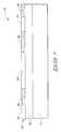
- FIG. 1is a cross-sectional view of a portion of a semiconductor-on-insulator (SOI) substrate at an early stage in the formation of a first transistor gate structure in accordance with embodiments of the present invention.
- SOIsemiconductor-on-insulator
- FIG. 2depicts the structure of FIG. 1 after additional processing in accordance with embodiments of the present invention.
- FIG. 2 ais an enlarged cross-sectional view of the indicated portion of FIG. 2 .
- FIG. 3depicts the structure of FIG. 2 after additional processing in accordance with embodiments of the present invention.
- FIG. 4depicts the structure of FIG. 2 after additional processing in accordance with embodiments of the present invention.
- FIG. 4 ais an enlarged cross-sectional view of the indicated portion of FIG. 4 .
- FIG. 5depicts the structure of FIG. 4 after additional processing in accordance with embodiments of the present invention.
- FIG. 5 ais an enlarged cross-sectional view of the indicated portion of FIG. 5 .
- FIG. 6depicts the structure of FIG. 5 after bonding to a handle wafer and additional processing in accordance with embodiments of the present invention.
- FIG. 7depicts the structure of FIG. 6 after additional processing in accordance with embodiments of the present invention.
- FIG. 8depicts the structure of FIG. 7 after additional processing to form a second transistor gate structure in accordance with embodiments of the present invention.
- FIG. 9depicts the structure of FIG. 8 after additional processing to form a second transistor gate structure in accordance with embodiments of the present invention.
- FIG. 1a cross-sectional view of a portion of semiconductor-on-insulator (SOI) substrate 10 at an early stage in the formation of a dual-gated transistor is depicted.
- a bulk or initial substrate 15is shown having an insulator layer 20 and a semiconductor or device layer 30 disposed thereover.
- Insulator layer 20generally encompasses a silicon oxide material, although other insulating materials such as silicon nitride or oxynitrides can be employed and often is referred to as a buried oxide or buried insulator layer.
- Insulator layer 20generally has a thickness in the range of about 20 nanometers (nm) to about 500 nm, with about 150 nm being typical.
- Bulk substrate 15is typically a lightly doped, conventional single crystal silicon substrate.
- SOI substrate 10is generally formed by any of the known, conventional methods for forming such substrates. These conventional methods include, but are not limited to, wafer bonding techniques, methods that employ an implantation such as SIMOX (separation by implanted oxygen), and ZMR (zone melting recrystallization). However, any other appropriate method of forming SOI substrate 10 that is known or that becomes known is within the scope and spirit of the present invention.
- layer 30is single crystal silicon material, although other appropriate semiconductor materials can be employed.
- Device layer 30generally has thickness in the range of from about 20 nanometers (nm) to about 200 nm where thickness of about 100 nm is typical.
- layer 30is generally formed having an appropriate concentration of either a P-type dopant or an N-type dopant, although in some embodiments the appropriate dopant is provided after device layer 30 is formed.
- Isolation regions 38are typically formed by conventional shallow trench isolation (STI) methods, although other appropriate isolation methods can also be used. Where an STI method is employed for forming isolation regions 38 , typically, portions of layer 30 are removed to form trenches (not shown) extending to and exposing underlying regions of insulation layer 20 . Such trenches are then filled with a dielectric material, for example silicon dioxide. After the filling, the structure is planarized, for example by a chemical mechanical polishing (CMP) process, to provide an essentially planar surface.
- CMPchemical mechanical polishing
- First gate structures 45are generally formed by conventional deposition, patterning and etching methods and encompass a first gate dielectric 40 , a first gate electrode 42 , a first conductive layer 44 and a first capping layer 46 .
- An exemplary gate dielectric materialis a silicon dioxide material formed to have a thickness of between about 2 nm to about 20 nm. A thickness, for gate dielectric 40 , of about 4 nm is typical.
- Embodiments of the present inventiongenerally employ a material encompassing polycrystalline silicon for gate electrode 42 , although other appropriate materials can be employed.
- Such polysilicon materialis generally formed using conventional low pressure chemical vapor deposition (LPCVD) methods and has a nominal thickness of about 80 nm. Some embodiments employ thicker or thinner polysilicon for first electrode 42 , the range from about 30 nm to about 200 nm being typical.
- First conductive layer 44is generally a silicide material such as titanium silicide, however, non-silicide materials such as titanium-tungsten (TiW) or tungsten (W) are also appropriate for conductive layer 44 .
- first capping layer 46is generally a dielectric material such as silicon dioxide, silicon nitride or an oxynitride, and is formed having an appropriate thickness in the range of from about 100 nm to about 300 nm.
- FIG. 2 ais used to depict source/drain (S/D) regions 33 , lightly doped drain (LDD) regions 35 and halo regions 37 which are operably adjacent first transistor gate structure 45 .
- S/Dsource/drain
- LDD regions 35are generally formed by implantation of an N-type dopant such as arsenic into active area regions 34 , gate structures 45 serving to mask or shield portions of region 34 , thereunder.
- a dose of about 9 E13 ions/cm 2 or greateris exemplary.
- First dielectric sidewall spacers 48are then formed, generally of silicon dioxide, silicon nitride or an oxynitride, laterally adjacent opposing sides of gate structures 45 .
- a second implant of an N-type dopantis used to form S/D regions 33 , spaced laterally outward from gate structure 45 , where gate structures 45 and spacers 48 serve to mask or shield portions of region 34 , thereunder.
- An arsenic dose of 2 E15 ions/cm 2 or greateris exemplary for the S/D forming implant.
- LDD and S/D implantsare performed at standard implantation angles, where an embodiment of the present invention employs halo regions 37 , an angled implantation of a dose of boron, or another appropriate P-type dopant, between about 2 E12 to about 2.5 E12 ions/cm 2 is generally employed. While the specific angle of the implant can vary as a function of the device characteristics desired, generally an angle of between about 10° to about 60° from normal is employed.
- some embodiments in accordance with the present inventionencompass P-channel devices and employ appropriate P-type dopants for S/D and LDD regions.
- Other embodimentsencompass additional regions to provide more extensively tailored S/D regions than described above and still other embodiments do not encompass halo regions 37 .
- embodiments of the present inventionalso include any of the various channel tailoring processes that can be employed, for example, some embodiments of the present invention include one or more threshold adjust implant processes.
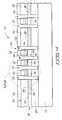
- FIG. 3depicts the structure of FIG. 2 subsequent to the initial forming of a first insulating layer 50 .
- first insulating layer 50encompasses both an initially formed conformal layer and a subsequently formed bulk layer.
- a conformal portion of layer 50is formed by a conventional chemical vapor deposition (CVD) process, such as one employing the low pressure and/or plasma enhanced decomposition of tetraethyl orthosilicate (TEOS), and has a thickness of between about 5 nm to 50 nm.
- the bulk portion of first layer 50while also generally employing a CVD process, is typically a borophosphosilicate glass (BPSG).
- BPSGborophosphosilicate glass
- the thickness of layer 50as formed, is nominally about 1000 nm which is sufficient to cover first gate structures 45 , although other total thickness that cover structures 45 are also appropriate.
- first insulating layer 50is planarized to form an essentially planar upper surface 53 of layer 50 .
- planarizationis accomplished using a CMP process.
- first capping layer 46encompasses silicon nitride
- advantageously such capping layer 46serves as a planarization stop such that upper surface 53 of layer 50 is essentially co-planar with an upper surface of such portions of capping layer 46 .
- a timed CMP processcan be employed such that upper surface 53 is elevationally above capping layer 46 (not shown).
- a masking layer 52is deposited and patterned to expose underlying portions of layer 50 , and an etch process is employed to define contact openings 55 .
- contact openings 55are shown extending through first insulating layer 50 , S/D regions 33 and into insulator layer 20 . While not shown, in some embodiments of the present invention, S/D contact openings 55 extend through insulator layer 20 and into bulk substrate 15 . It will be understood that the method employed for forming contact openings 55 is typically tailored for the specific materials of the several layers in which openings 55 are formed. Thus, in some embodiments of the present invention, an exemplary anisotropic etch is employed where the material of layer 50 is first etched with selectivity to the material of first spacers 48 such that no portion of gate electrode layer 42 or conducive layer 44 is exposed to opening 55 .
- Such first etchingcan be followed with a second etch for selectively etching through the material of S/D regions 33 , a third etch for selectively etching through the material of insulator layer 20 , and in embodiments where opening 55 extends into bulk substrate 10 , a fourth etch for selectively etching the material of bulk substrate 10 .
- FIGS. 5 and 5 aSOI wafer 10 is depicted after additional processing in accordance with embodiments of the present invention. Specifically, masking layer 52 is removed, contact openings 55 (FIG. 4) are filled with a conductive material and SOI wafer 10 planarized to form contact structures 58 and an essentially planar surface 54 .
- the material selected for forming S/D contact structures 58should exhibit good thermal stability characteristics during subsequent processing.
- the selected materialshould exhibit appropriate conductivity. Therefore, embodiments of the present invention typically employ a TiN/W material for filling contact openings 55 .
- other materialssuch as polysilicon, can be advantageously formed using simpler processing.
- polysilicon materialas known, will provide less conductivity than an otherwise equivalent TiN/W structure, embodiments of the present invention can employ polysilicon for contact structures 58 where appropriate.
- a TiN/W materialgenerally, an initial layer of TiN, or any other appropriate “adhesion layer” material, is formed to a nominal thickness of about 30 nm; the TiN forming an essentially conformal layer over the exposed surfaces of opening 55 . Subsequently, openings 55 are filled using a blanket CVD W deposition process which is followed by a CMP planarization process to complete the forming of contact structures 58 .
- polysiliconis employed for contact structures 58 , generally such is deposited in situ doped to provide appropriate conductivity for its purpose and is followed by a CMP planarization process to complete the forming of contact structures 58 . Referring to FIG.
- contact structures 58encompass a first portion that is adjacent sidewall spacers 48 and a second portion that extends from the first portion through S/D regions 33 and into insulator layer 20 , therebelow.
- structures 58by filling openings 55 (FIG. 3 a ), provide electrical contact to S/D regions 33 , and through such S/D regions 33 to first gate structures 45 .
- TiN/W and polysilicon materialsare described herein as being advantageously used by embodiments of the present invention, such use is not to the exclusion of other materials that exhibit appropriate conductivity and thermal stability with respect to subsequent processing, as described below. Hence, such other materials are also within the scope and spirit of the present invention.
- SOI wafer portion 10is shown after additional processing in accordance with embodiments of the present invention.
- a second insulating layer 60is shown overlying first layer 50 and first transistor gate structures 45 .
- Via contact structures 65are shown formed within second layer 60 and in contact with S/D contact structures 58 as well as conductive wiring structures 75 disposed over second insulating layer 60 .
- a third insulating layer 70disposed overlying wiring structures 75 and second layer 60 .
- Second insulating layer 60is generally a BPSG layer formed by conventional CVD processing to have a thickness in a range from about 500 nm to about 1200 nm with about 1000 nm being typical.
- Via contact structures 65can be formed by conventional or other appropriate methods.
- a masking layer(not shown) is formed and patterned, and openings formed and filled with a conductive material, generally a TiN/W material as described above, although in some embodiments, polysilicon is also appropriate.
- the material selected for forming structures 65should also exhibit appropriate conductivity and thermal stability with respect to subsequent processing. After forming such conductive fill material, some embodiments of the present invention complete the definition of structures 65 by planarization, for example a CMP process.
- a conductive material layeris deposited and patterned to form wiring structures 75 .
- an alternate damascene processis employed to form wiring structures 75 .
- Embodiments of the present inventiongenerally employ TiN/W for wiring structures 75 although other appropriate materials, for example polysilicon, copper or appropriate alloys of copper can also be used.
- wiring structures 75are overlaid with third insulating layer 70 which encompasses a silicon oxide comprising material.
- embodiments in accordance with the present inventionemploy a conventional CVD process to form layer 70 which is followed by a planarization process, typically a CMP process, to form planarized surface 72 .
- embodiments of the present inventionemploy layer 70 as a bonding or dielectric material layer. That is to say, in subsequent processing, a handle wafer will be bonded to SOI structure 10 at layer 70 . Therefore a thickness of layer 70 is provided that is sufficient for such a purpose.
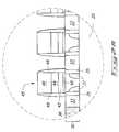
- FIG. 7SOI wafer portion 10 of FIG. 6 is shown after bonding to handle wafer 100 , and other additional processing in accordance with embodiments of the present invention to form a bonded structure 12 .
- FIG. 7depicts the structures of the previous illustrations “flipped” or inverted such that, for example, wiring structures 75 are oriented downward in the present illustration as opposed to the orientation of FIG. 6 .
- handle wafer 100As discussed above, the selection of conductive materials for the forming of S/D contact structures 58 , via contact structures 65 and wiring structures 75 in embodiments of the present invention, was made with consideration of thermal stability during subsequent processing.
- the bonding of handle wafer 100 to SOI substrateis that subsequent processing.
- a silicon handle waferis provided having an oxidized surface (not shown) which is pressed to a silicon oxide comprising layer disposed on a substrate, for embodiments of the present invention, layer 70 .
- the pressed together structuresare then heated to a bonding temperature of about 700° C., while pressed together, for a time sufficient for the bonding to occur.
- a device layeris exposed by lapping away bulk silicon such that the device layer overlies an insulator layer, the oxidized surfaces that were bonded, which overlies the handle wafer.
- the wafer bonding processforms a bonded substrate 12 having the previously formed first transistor structures and conductive structures disposed between handle wafer 100 and device layer 30 .
- insulating layers 50 , 60 and 70can be seen as the insulator layer, referred to herein as combined insulator layer 110 .
- FIG. 7depicts that original bulk substrate 15 is removed to expose a second side of original insulator layer 20 as well as portions of S/D contact structures 58 . As seen, the exposed second side of layer 20 is opposite the first side of such layer which is adjacent device layer 30 .
- material of bulk substrate 15is removed by an initial lapping process, which removes most of the substrate material, and a subsequent polishing process, for example a CMP process, for providing a polished upper surface 24 .
- a subsequent polishing processfor example a CMP process
- an implant and cleaving processcan be used in combination with the CMP process.
- embodiments in accordance with the present inventionuse contact structures 58 as etch stop indicators for the planarization process, thus providing surface 24 that encompasses both exposed portions of a second side of layer 20 and S/D contact structures 58 .
- S/D contact structures 58can provide an etch stop for the exemplary CMP process such that surface 24 encompasses essentially coplanar portions of such structures 58 and the second side of layer 20 , as depicted.
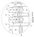
- bonded substrate 12is depicted after additional processing in accordance with an embodiment of the present invention. Specifically, portions of insulator layer 20 are removed from between adjacent S/D contact structures 58 to form openings 26 . Such removal can be accomplished by depositing a masking layer (not shown) and patterning the layer to expose the desired areas of layer 20 which are then etched by an appropriate etching process that selectively removes the material of layer 20 and not the material of contact structures 58 . In some embodiments of the present invention, an additional, peripheral portion of layer 20 is removed that is not disposed between two contact structures 58 to form peripheral opening or region 28 . As will be described below, region 28 can be advantageously used for the forming of optional peripheral circuitry operably adjacent the second side of device layer 30 using conventional or other appropriate processing.
- second dielectric spacers 22are formed laterally adjacent exposed sidewall portions of S/D contact structures 58 .
- additional dielectric spacers 25can advantageously be formed in a common processing step.
- Dielectric spacers 22 , and if formed, spacers 25are formed by conventional or other methods, for example a layer of a dielectric material such as a silicon dioxide, silicon nitride or oxynitride comprising material is deposited and etched back to provide spacers 22 and 25 .
- transistor gate structures 95 and optional peripheral transistor gate structure 98are formed using conventional or other appropriate methods.
- second transistor gate structures 95are self-aligned to first transistor gate structures 45 and to the channel region therebetween.
- S/D contact structures 58provide for the alignment of first and second transistor gate structures to one another.
- the self-alignment of the gate structures 45 and 95provided by embodiments in accordance with the present invention, advantageously provide that such transistors employ common S/D contact structures.
- a second gate dielectric 120is first formed and a second gate electrode 122 is second formed such that gate electrode 122 overlies gate dielectric 120 .
- the materials used for such second gate dielectric 120 and second gate electrode 122are the same materials employed for the opposing first transistor structure 45 , however in some embodiments of the present invention different materials and/or thickness are employed.
- first dielectric 40encompasses a silicon dioxide material
- second gate dielectric 120can encompass any appropriate alternate material.
- any appropriate materialcan be used for forming second gate electrode 122 , second conductive layer 124 and second capping layer 126 .
- Such appropriate materialscan include materials that will provide different threshold voltages for such second transistors.
- second capping layer 126is formed. For example, by such methods as described for the analogous first conductive layer 44 and first capping layer 46 . Some embodiments of the present invention employ alternate materials for second layer 124 and second layer 126 , formed by methods appropriate for the specific material selected. For example, where first capping layer 46 is formed of a silicon nitride comprising material employing a CVD process, second capping layer 126 can be formed of a silicon dioxide comprising material using a different, appropriate CVD process. It will be noted, that regardless of the process or material employed for forming capping layer 126 , typically such layer 126 is formed having a portion overlying surface 24 of insulator layer 20 as depicted.
- second gate structure 95being self-aligned to first transistor gate structure 45
- most of such structureis formed laterally adjacent and between dielectric spacers 22 such that the lateral dimensions of each of the gate dielectric 120 , the gate electrode 122 , the conductive layer 124 and a significant portion of capping layer 126 are fixed by the spacing between such spacers 22 and thus have essentially the same lateral dimension as first gate structure 45 . Therefore, preferred embodiments in accordance with the present invention advantageously do not require a separate etching step to define a lateral dimension for second gate structure 95 .
- an advantageous benefit of embodiments of the present inventionis a reduced lateral dimension of the gate structures as compared to previously known methods. Such a reduced lateral dimension being the result of not having to provide an “over-sized” gate structure for proper alignment of the first and second transistor gate structures. Furthermore the S/D capacitive coupling with the gate is reduced compared with known prior art.
- second capping layer 126after the forming of second capping layer 126 , generally some or all of such layer overlying surface 24 is removed. Where some of layer 126 is removed, as depicted, a conventional masking and etching process is typically employed. For embodiments of the present invention where all of capping layer 126 overlying surface 24 is removed, generally a planarization process, such as a CMP process, is employed.
- third transistor gate structure 98is provided, generally such structure is typically formed, at least in part, concurrently with second structure 95 . As such third gate structure 98 is not self-aligned to an underlying first gate structure 45 , and as such third structure is not formed laterally adjacent and between spacers 22 , third gate structure 98 , lateral dimensions of such structure are provided by a appropriate processing. Thus in some embodiments of the present invention, an etching process is employed to define both third gate structure 98 and to remove portions of capping layer 126 overlying surface 24 .
- third gate structure 98does not share a channel region or S/D regions with an opposing gate structure
- embodiments of the present inventionprovide for appropriate channel tailoring and S/D forming processes as are generally employed to provide such structures and/or regions, where such regions are required.
Landscapes
- Engineering & Computer Science (AREA)
- Physics & Mathematics (AREA)
- Condensed Matter Physics & Semiconductors (AREA)
- General Physics & Mathematics (AREA)
- Manufacturing & Machinery (AREA)
- Computer Hardware Design (AREA)
- Microelectronics & Electronic Packaging (AREA)
- Power Engineering (AREA)
- Thin Film Transistor (AREA)
Abstract
Description
Claims (32)
Priority Applications (3)
| Application Number | Priority Date | Filing Date | Title |
|---|---|---|---|
| US09/844,184US6593192B2 (en) | 2001-04-27 | 2001-04-27 | Method of forming a dual-gated semiconductor-on-insulator device |
| US10/455,975US6790732B2 (en) | 2001-04-27 | 2003-06-06 | Self-aligned dual-gate transistor device and method of forming self-aligned dual-gate transistor device |
| US10/932,192US7064036B2 (en) | 2001-04-27 | 2004-09-01 | Dual-gate transistor device and method of forming a dual-gate transistor device |
Applications Claiming Priority (1)
| Application Number | Priority Date | Filing Date | Title |
|---|---|---|---|
| US09/844,184US6593192B2 (en) | 2001-04-27 | 2001-04-27 | Method of forming a dual-gated semiconductor-on-insulator device |
Related Child Applications (1)
| Application Number | Title | Priority Date | Filing Date |
|---|---|---|---|
| US10/455,975ContinuationUS6790732B2 (en) | 2001-04-27 | 2003-06-06 | Self-aligned dual-gate transistor device and method of forming self-aligned dual-gate transistor device |
Publications (2)
| Publication Number | Publication Date |
|---|---|
| US20020160574A1 US20020160574A1 (en) | 2002-10-31 |
| US6593192B2true US6593192B2 (en) | 2003-07-15 |
Family
ID=25292057
Family Applications (3)
| Application Number | Title | Priority Date | Filing Date |
|---|---|---|---|
| US09/844,184Expired - LifetimeUS6593192B2 (en) | 2001-04-27 | 2001-04-27 | Method of forming a dual-gated semiconductor-on-insulator device |
| US10/455,975Expired - LifetimeUS6790732B2 (en) | 2001-04-27 | 2003-06-06 | Self-aligned dual-gate transistor device and method of forming self-aligned dual-gate transistor device |
| US10/932,192Expired - LifetimeUS7064036B2 (en) | 2001-04-27 | 2004-09-01 | Dual-gate transistor device and method of forming a dual-gate transistor device |
Family Applications After (2)
| Application Number | Title | Priority Date | Filing Date |
|---|---|---|---|
| US10/455,975Expired - LifetimeUS6790732B2 (en) | 2001-04-27 | 2003-06-06 | Self-aligned dual-gate transistor device and method of forming self-aligned dual-gate transistor device |
| US10/932,192Expired - LifetimeUS7064036B2 (en) | 2001-04-27 | 2004-09-01 | Dual-gate transistor device and method of forming a dual-gate transistor device |
Country Status (1)
| Country | Link |
|---|---|
| US (3) | US6593192B2 (en) |
Cited By (9)
| Publication number | Priority date | Publication date | Assignee | Title |
|---|---|---|---|---|
| US20030085424A1 (en)* | 2001-11-02 | 2003-05-08 | International Business Machines Corporation | Transistor structure with thick recessed source/drain structures and fabrication process of same |
| US20040014304A1 (en)* | 2002-07-18 | 2004-01-22 | Micron Technology, Inc. | Stable PD-SOI devices and methods |
| US20040046208A1 (en)* | 2002-09-05 | 2004-03-11 | International Business Machines Corporation | Polysilicon back-gated SOI MOSFET for dynamic threshold voltage control |
| US20040121549A1 (en)* | 2002-12-23 | 2004-06-24 | Dokumaci Omer H. | Self-aligned planar double-gate process by amorphization |
| US20050142703A1 (en)* | 2001-04-27 | 2005-06-30 | Zahurak John K. | Dual-gate transistor device and method of forming a dual-gate transistor device |
| US20050245009A1 (en)* | 2004-04-28 | 2005-11-03 | International Business Machines Corporation | Backgated finfet having diferent oxide thicknesses |
| US20070232003A1 (en)* | 2004-05-25 | 2007-10-04 | Koninklijke Philips Electronics N.C | Planar Dual Gate Semiconductor Device |
| US20100237351A1 (en)* | 2006-08-04 | 2010-09-23 | Nxp, B.V. | Method of manufacturing a double gate transistor |
| US20130069171A1 (en)* | 2010-08-17 | 2013-03-21 | International Business Machines Corporation | Controlled Fin-Merging for Fin Type FET Devices |
Families Citing this family (19)
| Publication number | Priority date | Publication date | Assignee | Title |
|---|---|---|---|---|
| US6982460B1 (en)* | 2000-07-07 | 2006-01-03 | International Business Machines Corporation | Self-aligned gate MOSFET with separate gates |
| KR100481868B1 (en)* | 2002-11-26 | 2005-04-11 | 삼성전자주식회사 | Modified silicon-on-insulator substrate having isolation structure of preventing leakage current and method of fabricating the same |
| US7271403B2 (en)* | 2002-12-13 | 2007-09-18 | Intel Corporation | Isolating phase change memory devices |
| US7173305B2 (en)* | 2003-04-08 | 2007-02-06 | Taiwan Semiconductor Manufacturing Company, Ltd. | Self-aligned contact for silicon-on-insulator devices |
| EP1665386A1 (en)* | 2003-09-03 | 2006-06-07 | Koninklijke Philips Electronics N.V. | Method of fabricating a double gate field effect transistor device, and such a double gate field effect transistor device |
| JP2005142481A (en)* | 2003-11-10 | 2005-06-02 | Nec Electronics Corp | Manufacturing method of semiconductor device |
| JP4610982B2 (en)* | 2003-11-11 | 2011-01-12 | シャープ株式会社 | Manufacturing method of semiconductor device |
| DE102004033149B4 (en)* | 2004-07-08 | 2006-09-28 | Infineon Technologies Ag | A method of fabricating a dual gate transistor, a memory cell, a vertical transistor, and buried word or bit lines, each using a buried etch stop layer |
| FR2899381B1 (en)* | 2006-03-28 | 2008-07-18 | Commissariat Energie Atomique | METHOD FOR PRODUCING A SELF-ALIGNED GRID FIELD EFFECT TRANSISTOR |
| US7531879B2 (en)* | 2006-12-22 | 2009-05-12 | Intel Corporation | Method and resultant structure for floating body memory on bulk wafer |
| US7923840B2 (en)* | 2007-01-10 | 2011-04-12 | International Business Machines Corporation | Electrically conductive path forming below barrier oxide layer and integrated circuit |
| US9460924B2 (en)* | 2007-03-26 | 2016-10-04 | GlobalFoundries, Inc. | Semiconductor device having structure with fractional dimension of the minimum dimension of a lithography system |
| US7635648B2 (en)* | 2008-04-10 | 2009-12-22 | Applied Materials, Inc. | Methods for fabricating dual material gate in a semiconductor device |
| US9219129B2 (en)* | 2012-05-10 | 2015-12-22 | International Business Machines Corporation | Inverted thin channel mosfet with self-aligned expanded source/drain |
| US8940569B2 (en)* | 2012-10-15 | 2015-01-27 | International Business Machines Corporation | Dual-gate bio/chem sensor |
| US9059123B2 (en) | 2013-07-24 | 2015-06-16 | International Business Machines Corporation | Active matrix using hybrid integrated circuit and bipolar transistor |
| US9530798B1 (en)* | 2015-06-24 | 2016-12-27 | Globalfoundries Inc. | High performance heat shields with reduced capacitance |
| US9786546B1 (en)* | 2016-04-06 | 2017-10-10 | International Business Machines Corporation | Bulk to silicon on insulator device |
| KR102795666B1 (en) | 2019-08-02 | 2025-04-15 | 삼성전자주식회사 | Semiconductor devices |
Citations (15)
| Publication number | Priority date | Publication date | Assignee | Title |
|---|---|---|---|---|
| US5115289A (en)* | 1988-11-21 | 1992-05-19 | Hitachi, Ltd. | Semiconductor device and semiconductor memory device |
| US5164805A (en)* | 1988-08-22 | 1992-11-17 | Massachusetts Institute Of Technology | Near-intrinsic thin-film SOI FETS |
| US5621239A (en) | 1990-11-05 | 1997-04-15 | Fujitsu Limited | SOI device having a buried layer of reduced resistivity |
| US5646058A (en)* | 1994-07-15 | 1997-07-08 | International Business Machines Corporation | Method for fabricating a self-aligned double-gate MOSFET by selective lateral epitaxy |
| US5736435A (en) | 1995-07-03 | 1998-04-07 | Motorola, Inc. | Process for fabricating a fully self-aligned soi mosfet |
| US5885887A (en)* | 1997-04-21 | 1999-03-23 | Advanced Micro Devices, Inc. | Method of making an igfet with selectively doped multilevel polysilicon gate |
| US6004837A (en) | 1998-02-18 | 1999-12-21 | International Business Machines Corporation | Dual-gate SOI transistor |
| US6063686A (en) | 1993-11-05 | 2000-05-16 | Masuda; Hiroo | Method of manufacturing an improved SOI (silicon-on-insulator) semiconductor integrated circuit device |
| US6121661A (en)* | 1996-12-11 | 2000-09-19 | International Business Machines Corporation | Silicon-on-insulator structure for electrostatic discharge protection and improved heat dissipation |
| US6284594B1 (en)* | 2000-05-30 | 2001-09-04 | Chartered Semiconductor Manufacturing Ltd. | Formation of an interpoly capacitor structure using a chemical mechanical polishing procedure |
| US6337505B2 (en)* | 1998-04-02 | 2002-01-08 | Hyundai Electronics Industries Co., Ltd. | Semiconductor device and method for fabricating the same |
| US6365450B1 (en)* | 2001-03-15 | 2002-04-02 | Advanced Micro Devices, Inc. | Fabrication of P-channel field effect transistor with minimized degradation of metal oxide gate |
| US6376312B1 (en)* | 2001-03-26 | 2002-04-23 | Advanced Micro Devices, Inc. | Formation of non-volatile memory device comprised of an array of vertical field effect transistor structures |
| US6391752B1 (en)* | 2000-09-12 | 2002-05-21 | Taiwan Semiconductor Manufacturing, Co., Ltd. | Method of fabricating a silicon-on-insulator semiconductor device with an implanted ground plane |
| US6396108B1 (en)* | 2000-11-13 | 2002-05-28 | Advanced Micro Devices, Inc. | Self-aligned double gate silicon-on-insulator (SOI) device |
Family Cites Families (22)
| Publication number | Priority date | Publication date | Assignee | Title |
|---|---|---|---|---|
| EP0465229B1 (en) | 1990-07-02 | 1994-12-28 | Seiko Epson Corporation | Micropump and process for manufacturing a micropump |
| US5154661A (en) | 1991-07-10 | 1992-10-13 | Noah Precision, Inc. | Thermal electric cooling system and method |
| US5313094A (en) | 1992-01-28 | 1994-05-17 | International Business Machines Corportion | Thermal dissipation of integrated circuits using diamond paths |
| US5262352A (en)* | 1992-08-31 | 1993-11-16 | Motorola, Inc. | Method for forming an interconnection structure for conductive layers |
| US5621339A (en)* | 1993-09-14 | 1997-04-15 | Crystal Semiconductor | Method and apparatus for removing trapped oxide charge from a differential input stage |
| US5793107A (en) | 1993-10-29 | 1998-08-11 | Vlsi Technology, Inc. | Polysilicon pillar heat sinks for semiconductor on insulator circuits |
| CH689836A5 (en) | 1994-01-14 | 1999-12-15 | Westonbridge Int Ltd | Micropump. |
| US5753529A (en) | 1994-05-05 | 1998-05-19 | Siliconix Incorporated | Surface mount and flip chip technology for total integrated circuit isolation |
| JP2986381B2 (en) | 1994-08-16 | 1999-12-06 | インターナショナル・ビジネス・マシーンズ・コーポレイション | Electronic chip temperature control device and method |
| US5767578A (en) | 1994-10-12 | 1998-06-16 | Siliconix Incorporated | Surface mount and flip chip technology with diamond film passivation for total integated circuit isolation |
| KR100239414B1 (en)* | 1996-11-07 | 2000-01-15 | 김영환 | Fabricating method of semiconductor device |
| US6336312B1 (en)* | 1997-02-03 | 2002-01-08 | Textron Inc. | Gang-Type rotary lawn mower with multiple rear rollers |
| DE19929210C1 (en)* | 1999-06-25 | 2000-10-26 | Infineon Technologies Ag | Substrate used as a SOI substrate comprises a layer of monocrystalline silicon, a silicon dioxide layer and a silicon substrate |
| US6320225B1 (en)* | 1999-07-13 | 2001-11-20 | International Business Machines Corporation | SOI CMOS body contact through gate, self-aligned to source- drain diffusions |
| US6573565B2 (en)* | 1999-07-28 | 2003-06-03 | International Business Machines Corporation | Method and structure for providing improved thermal conduction for silicon semiconductor devices |
| JP2001102550A (en)* | 1999-09-02 | 2001-04-13 | Samsung Electronics Co Ltd | Semiconductor memory device having self-aligned contact and method of manufacturing the same |
| US6393752B1 (en)* | 1999-10-04 | 2002-05-28 | Keith P. Oliver | Mounting device of pistol laser site |
| US6573656B2 (en)* | 2000-07-14 | 2003-06-03 | Matsushita Electric Industrial Co., Ltd. | High-pressure discharge lamp and method for producing the same |
| US6429477B1 (en)* | 2000-10-31 | 2002-08-06 | International Business Machines Corporation | Shared body and diffusion contact structure and method for fabricating same |
| US6320325B1 (en)* | 2000-11-06 | 2001-11-20 | Eastman Kodak Company | Emissive display with luminance feedback from a representative pixel |
| US6406962B1 (en)* | 2001-01-17 | 2002-06-18 | International Business Machines Corporation | Vertical trench-formed dual-gate FET device structure and method for creation |
| US6593192B2 (en)* | 2001-04-27 | 2003-07-15 | Micron Technology, Inc. | Method of forming a dual-gated semiconductor-on-insulator device |
- 2001
- 2001-04-27USUS09/844,184patent/US6593192B2/ennot_activeExpired - Lifetime
- 2003
- 2003-06-06USUS10/455,975patent/US6790732B2/ennot_activeExpired - Lifetime
- 2004
- 2004-09-01USUS10/932,192patent/US7064036B2/ennot_activeExpired - Lifetime
Patent Citations (15)
| Publication number | Priority date | Publication date | Assignee | Title |
|---|---|---|---|---|
| US5164805A (en)* | 1988-08-22 | 1992-11-17 | Massachusetts Institute Of Technology | Near-intrinsic thin-film SOI FETS |
| US5115289A (en)* | 1988-11-21 | 1992-05-19 | Hitachi, Ltd. | Semiconductor device and semiconductor memory device |
| US5621239A (en) | 1990-11-05 | 1997-04-15 | Fujitsu Limited | SOI device having a buried layer of reduced resistivity |
| US6063686A (en) | 1993-11-05 | 2000-05-16 | Masuda; Hiroo | Method of manufacturing an improved SOI (silicon-on-insulator) semiconductor integrated circuit device |
| US5646058A (en)* | 1994-07-15 | 1997-07-08 | International Business Machines Corporation | Method for fabricating a self-aligned double-gate MOSFET by selective lateral epitaxy |
| US5736435A (en) | 1995-07-03 | 1998-04-07 | Motorola, Inc. | Process for fabricating a fully self-aligned soi mosfet |
| US6121661A (en)* | 1996-12-11 | 2000-09-19 | International Business Machines Corporation | Silicon-on-insulator structure for electrostatic discharge protection and improved heat dissipation |
| US5885887A (en)* | 1997-04-21 | 1999-03-23 | Advanced Micro Devices, Inc. | Method of making an igfet with selectively doped multilevel polysilicon gate |
| US6004837A (en) | 1998-02-18 | 1999-12-21 | International Business Machines Corporation | Dual-gate SOI transistor |
| US6337505B2 (en)* | 1998-04-02 | 2002-01-08 | Hyundai Electronics Industries Co., Ltd. | Semiconductor device and method for fabricating the same |
| US6284594B1 (en)* | 2000-05-30 | 2001-09-04 | Chartered Semiconductor Manufacturing Ltd. | Formation of an interpoly capacitor structure using a chemical mechanical polishing procedure |
| US6391752B1 (en)* | 2000-09-12 | 2002-05-21 | Taiwan Semiconductor Manufacturing, Co., Ltd. | Method of fabricating a silicon-on-insulator semiconductor device with an implanted ground plane |
| US6396108B1 (en)* | 2000-11-13 | 2002-05-28 | Advanced Micro Devices, Inc. | Self-aligned double gate silicon-on-insulator (SOI) device |
| US6365450B1 (en)* | 2001-03-15 | 2002-04-02 | Advanced Micro Devices, Inc. | Fabrication of P-channel field effect transistor with minimized degradation of metal oxide gate |
| US6376312B1 (en)* | 2001-03-26 | 2002-04-23 | Advanced Micro Devices, Inc. | Formation of non-volatile memory device comprised of an array of vertical field effect transistor structures |
Non-Patent Citations (7)
| Title |
|---|
| Frank, D., et al.; "Monte Carlo Simulation of a 30nm Dual-Gate MOSFET: How Short Can Si Go?", IEEE 1992, pp. 553-556. |
| Hisamoto, D., et al.; A Fully Depleted Lean Channel Transistor (DELTA) -novel vertical ultra thin SOI MOSFET-; IEEE 1989, pp. 833-836. |
| Radack, Daniel J., "Advanced Microelectronics: The Role of SOI", IEEE International SOI Conference, Oct. 1990, pp. 5-7. |
| Sunouchi, k., et al.; "A Surrounding Gate Transistor (SGT) Cell for 64/256Mbit DRAMs", IEEE 1989, pp. 23-24 and 26. |
| Tanaka, T., et al., "Analysis of P+ Poly Si Double-Gate Thin-Film SOI MOSFETS", IEEE 1991, pp. 683-686. |
| Tanaka, T., et al.; "Ultrafast Operation of Vth -Adjusted p+-n+ Double-Gate SOI MOSFET's"; IEEE 1994, pp. 386-388. |
| Wann, C., et al., "A Comparative Study of Advanced MOSEFET Concepts", IEEE Oct. 1996, pp. 1742-1752. |
Cited By (28)
| Publication number | Priority date | Publication date | Assignee | Title |
|---|---|---|---|---|
| US7064036B2 (en)* | 2001-04-27 | 2006-06-20 | Micron Technology, Inc. | Dual-gate transistor device and method of forming a dual-gate transistor device |
| US20050142703A1 (en)* | 2001-04-27 | 2005-06-30 | Zahurak John K. | Dual-gate transistor device and method of forming a dual-gate transistor device |
| US6870225B2 (en)* | 2001-11-02 | 2005-03-22 | International Business Machines Corporation | Transistor structure with thick recessed source/drain structures and fabrication process of same |
| US20030085424A1 (en)* | 2001-11-02 | 2003-05-08 | International Business Machines Corporation | Transistor structure with thick recessed source/drain structures and fabrication process of same |
| US7288819B2 (en) | 2002-07-18 | 2007-10-30 | Micron Technology, Inc. | Stable PD-SOI devices and methods |
| US6828632B2 (en) | 2002-07-18 | 2004-12-07 | Micron Technology, Inc. | Stable PD-SOI devices and methods |
| US20050023613A1 (en)* | 2002-07-18 | 2005-02-03 | Micron Technology, Inc. | Stable PD-SOI devices and methods |
| US20050023578A1 (en)* | 2002-07-18 | 2005-02-03 | Micron Technology, Inc. | Stable PD-SOI devices and methods |
| US7485504B2 (en) | 2002-07-18 | 2009-02-03 | Micron Technology, Inc. | Stable PD-SOI devices and methods |
| US20060246680A1 (en)* | 2002-07-18 | 2006-11-02 | Micron Technology, Inc. | Stable PD-SOI devices and methods |
| US20040014304A1 (en)* | 2002-07-18 | 2004-01-22 | Micron Technology, Inc. | Stable PD-SOI devices and methods |
| US7268022B2 (en) | 2002-07-18 | 2007-09-11 | Micron Technology, Inc. | Stable PD-SOI devices and methods |
| US6815296B2 (en)* | 2002-09-05 | 2004-11-09 | International Business Machines Corporation | Polysilicon back-gated SOI MOSFET for dynamic threshold voltage control |
| US20040046208A1 (en)* | 2002-09-05 | 2004-03-11 | International Business Machines Corporation | Polysilicon back-gated SOI MOSFET for dynamic threshold voltage control |
| US6833569B2 (en) | 2002-12-23 | 2004-12-21 | International Business Machines Corporation | Self-aligned planar double-gate process by amorphization |
| US20040121549A1 (en)* | 2002-12-23 | 2004-06-24 | Dokumaci Omer H. | Self-aligned planar double-gate process by amorphization |
| US20060145195A1 (en)* | 2004-04-28 | 2006-07-06 | International Business Machines Corporation | Backgated finfet having different oxide thicknesses |
| US7187042B2 (en) | 2004-04-28 | 2007-03-06 | International Business Machines Corporation | Backgated FinFET having different oxide thicknesses |
| US20060237774A1 (en)* | 2004-04-28 | 2006-10-26 | International Business Machines Corporation | Backgated finfet having different oxide thicknesses |
| US7056773B2 (en) | 2004-04-28 | 2006-06-06 | International Business Machines Corporation | Backgated FinFET having different oxide thicknesses |
| US7476946B2 (en) | 2004-04-28 | 2009-01-13 | International Business Machines Corporation | Backgated FinFET having different oxide thicknesses |
| US20050245009A1 (en)* | 2004-04-28 | 2005-11-03 | International Business Machines Corporation | Backgated finfet having diferent oxide thicknesses |
| US20070232003A1 (en)* | 2004-05-25 | 2007-10-04 | Koninklijke Philips Electronics N.C | Planar Dual Gate Semiconductor Device |
| US7407844B2 (en) | 2004-05-25 | 2008-08-05 | Nxp B.V. | Planar dual gate semiconductor device |
| US20100237351A1 (en)* | 2006-08-04 | 2010-09-23 | Nxp, B.V. | Method of manufacturing a double gate transistor |
| US8183116B2 (en) | 2006-08-04 | 2012-05-22 | Nxp B.V. | Method of manufacturing a double gate transistor |
| US20130069171A1 (en)* | 2010-08-17 | 2013-03-21 | International Business Machines Corporation | Controlled Fin-Merging for Fin Type FET Devices |
| US8564064B2 (en)* | 2010-08-17 | 2013-10-22 | International Business Machines Corporation | Controlled fin-merging for fin type FET devices |
Also Published As
| Publication number | Publication date |
|---|---|
| US7064036B2 (en) | 2006-06-20 |
| US20020160574A1 (en) | 2002-10-31 |
| US6790732B2 (en) | 2004-09-14 |
| US20050142703A1 (en) | 2005-06-30 |
| US20030215988A1 (en) | 2003-11-20 |
Similar Documents
| Publication | Publication Date | Title |
|---|---|---|
| US6593192B2 (en) | Method of forming a dual-gated semiconductor-on-insulator device | |
| US7384850B2 (en) | Methods of forming complementary metal oxide semiconductor (CMOS) transistors having three-dimensional channel regions therein | |
| US6472258B1 (en) | Double gate trench transistor | |
| US5777370A (en) | Trench isolation of field effect transistors | |
| US6737308B2 (en) | Semiconductor device having LDD-type source/drain regions and fabrication method thereof | |
| US7018873B2 (en) | Method of making a device threshold control of front-gate silicon-on-insulator MOSFET using a self-aligned back-gate | |
| KR100189966B1 (en) | Soy-structured MOS transistor and manufacturing method thereof | |
| US7132339B2 (en) | Transistor structure with thick recessed source/drain structures and fabrication process of same | |
| US6815296B2 (en) | Polysilicon back-gated SOI MOSFET for dynamic threshold voltage control | |
| US5736435A (en) | Process for fabricating a fully self-aligned soi mosfet | |
| US7273785B2 (en) | Method to control device threshold of SOI MOSFET's | |
| US8017461B2 (en) | Methods of forming semiconductor-on-insulating (SOI) field effect transistors with body contacts | |
| US6174754B1 (en) | Methods for formation of silicon-on-insulator (SOI) and source/drain-on-insulator(SDOI) transistors | |
| US20070057288A1 (en) | Methods of Fabricating Semiconductor Devices with Enlarged Recessed Gate Electrodes | |
| US10446435B2 (en) | Local trap-rich isolation | |
| JPH11274496A (en) | FIELD EFFECT TRANSISTOR HAVING IMPROVED IMPLANT AND METHOD OF MANUFACTURING THE SAME | |
| US6403485B1 (en) | Method to form a low parasitic capacitance pseudo-SOI CMOS device | |
| US7081387B2 (en) | Damascene gate multi-mesa MOSFET | |
| US8680617B2 (en) | Split level shallow trench isolation for area efficient body contacts in SOI MOSFETS | |
| US6300172B1 (en) | Method of field isolation in silicon-on-insulator technology | |
| US8329519B2 (en) | Methods for fabricating a semiconductor device having decreased contact resistance | |
| US7391096B2 (en) | STI structure | |
| US20030089948A1 (en) | Substrate contact in SOI and method therefor | |
| US10079248B2 (en) | Field-effect transistors with a buried body contact | |
| US6511890B2 (en) | Method of fabricating a semiconductor device |
Legal Events
| Date | Code | Title | Description |
|---|---|---|---|
| AS | Assignment | Owner name:MICRON TECHNOLOGY, INC., IDAHO Free format text:ASSIGNMENT OF ASSIGNORS INTEREST;ASSIGNOR:DENNSION, CHARLES H.;REEL/FRAME:011757/0374 Effective date:20010419 | |
| STCF | Information on status: patent grant | Free format text:PATENTED CASE | |
| CC | Certificate of correction | ||
| FPAY | Fee payment | Year of fee payment:4 | |
| FPAY | Fee payment | Year of fee payment:8 | |
| FPAY | Fee payment | Year of fee payment:12 | |
| AS | Assignment | Owner name:U.S. BANK NATIONAL ASSOCIATION, AS COLLATERAL AGENT, CALIFORNIA Free format text:SECURITY INTEREST;ASSIGNOR:MICRON TECHNOLOGY, INC.;REEL/FRAME:038669/0001 Effective date:20160426 Owner name:U.S. BANK NATIONAL ASSOCIATION, AS COLLATERAL AGEN Free format text:SECURITY INTEREST;ASSIGNOR:MICRON TECHNOLOGY, INC.;REEL/FRAME:038669/0001 Effective date:20160426 | |
| AS | Assignment | Owner name:MORGAN STANLEY SENIOR FUNDING, INC., AS COLLATERAL AGENT, MARYLAND Free format text:PATENT SECURITY AGREEMENT;ASSIGNOR:MICRON TECHNOLOGY, INC.;REEL/FRAME:038954/0001 Effective date:20160426 Owner name:MORGAN STANLEY SENIOR FUNDING, INC., AS COLLATERAL Free format text:PATENT SECURITY AGREEMENT;ASSIGNOR:MICRON TECHNOLOGY, INC.;REEL/FRAME:038954/0001 Effective date:20160426 | |
| AS | Assignment | Owner name:U.S. BANK NATIONAL ASSOCIATION, AS COLLATERAL AGENT, CALIFORNIA Free format text:CORRECTIVE ASSIGNMENT TO CORRECT THE REPLACE ERRONEOUSLY FILED PATENT #7358718 WITH THE CORRECT PATENT #7358178 PREVIOUSLY RECORDED ON REEL 038669 FRAME 0001. ASSIGNOR(S) HEREBY CONFIRMS THE SECURITY INTEREST;ASSIGNOR:MICRON TECHNOLOGY, INC.;REEL/FRAME:043079/0001 Effective date:20160426 Owner name:U.S. BANK NATIONAL ASSOCIATION, AS COLLATERAL AGEN Free format text:CORRECTIVE ASSIGNMENT TO CORRECT THE REPLACE ERRONEOUSLY FILED PATENT #7358718 WITH THE CORRECT PATENT #7358178 PREVIOUSLY RECORDED ON REEL 038669 FRAME 0001. ASSIGNOR(S) HEREBY CONFIRMS THE SECURITY INTEREST;ASSIGNOR:MICRON TECHNOLOGY, INC.;REEL/FRAME:043079/0001 Effective date:20160426 | |
| AS | Assignment | Owner name:JPMORGAN CHASE BANK, N.A., AS COLLATERAL AGENT, ILLINOIS Free format text:SECURITY INTEREST;ASSIGNORS:MICRON TECHNOLOGY, INC.;MICRON SEMICONDUCTOR PRODUCTS, INC.;REEL/FRAME:047540/0001 Effective date:20180703 Owner name:JPMORGAN CHASE BANK, N.A., AS COLLATERAL AGENT, IL Free format text:SECURITY INTEREST;ASSIGNORS:MICRON TECHNOLOGY, INC.;MICRON SEMICONDUCTOR PRODUCTS, INC.;REEL/FRAME:047540/0001 Effective date:20180703 | |
| AS | Assignment | Owner name:MICRON TECHNOLOGY, INC., IDAHO Free format text:RELEASE BY SECURED PARTY;ASSIGNOR:U.S. BANK NATIONAL ASSOCIATION, AS COLLATERAL AGENT;REEL/FRAME:047243/0001 Effective date:20180629 | |
| AS | Assignment | Owner name:MICRON TECHNOLOGY, INC., IDAHO Free format text:RELEASE BY SECURED PARTY;ASSIGNOR:MORGAN STANLEY SENIOR FUNDING, INC., AS COLLATERAL AGENT;REEL/FRAME:050937/0001 Effective date:20190731 | |
| AS | Assignment | Owner name:MICRON SEMICONDUCTOR PRODUCTS, INC., IDAHO Free format text:RELEASE BY SECURED PARTY;ASSIGNOR:JPMORGAN CHASE BANK, N.A., AS COLLATERAL AGENT;REEL/FRAME:051028/0001 Effective date:20190731 Owner name:MICRON TECHNOLOGY, INC., IDAHO Free format text:RELEASE BY SECURED PARTY;ASSIGNOR:JPMORGAN CHASE BANK, N.A., AS COLLATERAL AGENT;REEL/FRAME:051028/0001 Effective date:20190731 |