US6590258B2 - SIO stacked DRAM logic - Google Patents
SIO stacked DRAM logicDownload PDFInfo
- Publication number
- US6590258B2 US6590258B2US09/998,318US99831801AUS6590258B2US 6590258 B2US6590258 B2US 6590258B2US 99831801 AUS99831801 AUS 99831801AUS 6590258 B2US6590258 B2US 6590258B2
- Authority
- US
- United States
- Prior art keywords
- layer
- integrated circuit
- insulator
- semiconductor layer
- circuit elements
- Prior art date
- Legal status (The legal status is an assumption and is not a legal conclusion. Google has not performed a legal analysis and makes no representation as to the accuracy of the status listed.)
- Expired - Fee Related
Links
Images


Classifications
- H—ELECTRICITY
- H10—SEMICONDUCTOR DEVICES; ELECTRIC SOLID-STATE DEVICES NOT OTHERWISE PROVIDED FOR
- H10B—ELECTRONIC MEMORY DEVICES
- H10B12/00—Dynamic random access memory [DRAM] devices
- H10B12/01—Manufacture or treatment
- H10B12/02—Manufacture or treatment for one transistor one-capacitor [1T-1C] memory cells
- H10B12/03—Making the capacitor or connections thereto
- H10B12/038—Making the capacitor or connections thereto the capacitor being in a trench in the substrate
- H10B12/0385—Making a connection between the transistor and the capacitor, e.g. buried strap
- H—ELECTRICITY
- H01—ELECTRIC ELEMENTS
- H01L—SEMICONDUCTOR DEVICES NOT COVERED BY CLASS H10
- H01L23/00—Details of semiconductor or other solid state devices
- H01L23/48—Arrangements for conducting electric current to or from the solid state body in operation, e.g. leads, terminal arrangements ; Selection of materials therefor
- H01L23/481—Internal lead connections, e.g. via connections, feedthrough structures
- H—ELECTRICITY
- H01—ELECTRIC ELEMENTS
- H01L—SEMICONDUCTOR DEVICES NOT COVERED BY CLASS H10
- H01L23/00—Details of semiconductor or other solid state devices
- H01L23/52—Arrangements for conducting electric current within the device in operation from one component to another, i.e. interconnections, e.g. wires, lead frames
- H01L23/535—Arrangements for conducting electric current within the device in operation from one component to another, i.e. interconnections, e.g. wires, lead frames including internal interconnections, e.g. cross-under constructions
- H—ELECTRICITY
- H10—SEMICONDUCTOR DEVICES; ELECTRIC SOLID-STATE DEVICES NOT OTHERWISE PROVIDED FOR
- H10D—INORGANIC ELECTRIC SEMICONDUCTOR DEVICES
- H10D86/00—Integrated devices formed in or on insulating or conducting substrates, e.g. formed in silicon-on-insulator [SOI] substrates or on stainless steel or glass substrates
- H10D86/201—Integrated devices formed in or on insulating or conducting substrates, e.g. formed in silicon-on-insulator [SOI] substrates or on stainless steel or glass substrates the substrates comprising an insulating layer on a semiconductor body, e.g. SOI
- H—ELECTRICITY
- H01—ELECTRIC ELEMENTS
- H01L—SEMICONDUCTOR DEVICES NOT COVERED BY CLASS H10
- H01L22/00—Testing or measuring during manufacture or treatment; Reliability measurements, i.e. testing of parts without further processing to modify the parts as such; Structural arrangements therefor
- H01L22/30—Structural arrangements specially adapted for testing or measuring during manufacture or treatment, or specially adapted for reliability measurements
- H01L22/32—Additional lead-in metallisation on a device or substrate, e.g. additional pads or pad portions, lines in the scribe line, sacrificed conductors
- H—ELECTRICITY
- H01—ELECTRIC ELEMENTS
- H01L—SEMICONDUCTOR DEVICES NOT COVERED BY CLASS H10
- H01L2924/00—Indexing scheme for arrangements or methods for connecting or disconnecting semiconductor or solid-state bodies as covered by H01L24/00
- H01L2924/0001—Technical content checked by a classifier
- H01L2924/0002—Not covered by any one of groups H01L24/00, H01L24/00 and H01L2224/00
- H—ELECTRICITY
- H10—SEMICONDUCTOR DEVICES; ELECTRIC SOLID-STATE DEVICES NOT OTHERWISE PROVIDED FOR
- H10B—ELECTRONIC MEMORY DEVICES
- H10B12/00—Dynamic random access memory [DRAM] devices
- H10B12/30—DRAM devices comprising one-transistor - one-capacitor [1T-1C] memory cells
- H10B12/37—DRAM devices comprising one-transistor - one-capacitor [1T-1C] memory cells the capacitor being at least partially in a trench in the substrate
- H10B12/373—DRAM devices comprising one-transistor - one-capacitor [1T-1C] memory cells the capacitor being at least partially in a trench in the substrate the capacitor extending under or around the transistor
- Y—GENERAL TAGGING OF NEW TECHNOLOGICAL DEVELOPMENTS; GENERAL TAGGING OF CROSS-SECTIONAL TECHNOLOGIES SPANNING OVER SEVERAL SECTIONS OF THE IPC; TECHNICAL SUBJECTS COVERED BY FORMER USPC CROSS-REFERENCE ART COLLECTIONS [XRACs] AND DIGESTS
- Y10—TECHNICAL SUBJECTS COVERED BY FORMER USPC
- Y10S—TECHNICAL SUBJECTS COVERED BY FORMER USPC CROSS-REFERENCE ART COLLECTIONS [XRACs] AND DIGESTS
- Y10S977/00—Nanotechnology
- Y10S977/70—Nanostructure
- Y10S977/701—Integrated with dissimilar structures on a common substrate
- Y10S977/712—Integrated with dissimilar structures on a common substrate formed from plural layers of nanosized material, e.g. stacked structures
- Y—GENERAL TAGGING OF NEW TECHNOLOGICAL DEVELOPMENTS; GENERAL TAGGING OF CROSS-SECTIONAL TECHNOLOGIES SPANNING OVER SEVERAL SECTIONS OF THE IPC; TECHNICAL SUBJECTS COVERED BY FORMER USPC CROSS-REFERENCE ART COLLECTIONS [XRACs] AND DIGESTS
- Y10—TECHNICAL SUBJECTS COVERED BY FORMER USPC
- Y10S—TECHNICAL SUBJECTS COVERED BY FORMER USPC CROSS-REFERENCE ART COLLECTIONS [XRACs] AND DIGESTS
- Y10S977/00—Nanotechnology
- Y10S977/70—Nanostructure
- Y10S977/701—Integrated with dissimilar structures on a common substrate
- Y10S977/72—On an electrically conducting, semi-conducting, or semi-insulating substrate
- Y10S977/721—On a silicon substrate
- Y—GENERAL TAGGING OF NEW TECHNOLOGICAL DEVELOPMENTS; GENERAL TAGGING OF CROSS-SECTIONAL TECHNOLOGIES SPANNING OVER SEVERAL SECTIONS OF THE IPC; TECHNICAL SUBJECTS COVERED BY FORMER USPC CROSS-REFERENCE ART COLLECTIONS [XRACs] AND DIGESTS
- Y10—TECHNICAL SUBJECTS COVERED BY FORMER USPC
- Y10S—TECHNICAL SUBJECTS COVERED BY FORMER USPC CROSS-REFERENCE ART COLLECTIONS [XRACs] AND DIGESTS
- Y10S977/00—Nanotechnology
- Y10S977/70—Nanostructure
- Y10S977/778—Nanostructure within specified host or matrix material, e.g. nanocomposite films
- Y10S977/779—Possessing nanosized particles, powders, flakes, or clusters other than simple atomic impurity doping
- Y—GENERAL TAGGING OF NEW TECHNOLOGICAL DEVELOPMENTS; GENERAL TAGGING OF CROSS-SECTIONAL TECHNOLOGIES SPANNING OVER SEVERAL SECTIONS OF THE IPC; TECHNICAL SUBJECTS COVERED BY FORMER USPC CROSS-REFERENCE ART COLLECTIONS [XRACs] AND DIGESTS
- Y10—TECHNICAL SUBJECTS COVERED BY FORMER USPC
- Y10S—TECHNICAL SUBJECTS COVERED BY FORMER USPC CROSS-REFERENCE ART COLLECTIONS [XRACs] AND DIGESTS
- Y10S977/00—Nanotechnology
- Y10S977/84—Manufacture, treatment, or detection of nanostructure
- Y10S977/90—Manufacture, treatment, or detection of nanostructure having step or means utilizing mechanical or thermal property, e.g. pressure, heat
- Y—GENERAL TAGGING OF NEW TECHNOLOGICAL DEVELOPMENTS; GENERAL TAGGING OF CROSS-SECTIONAL TECHNOLOGIES SPANNING OVER SEVERAL SECTIONS OF THE IPC; TECHNICAL SUBJECTS COVERED BY FORMER USPC CROSS-REFERENCE ART COLLECTIONS [XRACs] AND DIGESTS
- Y10—TECHNICAL SUBJECTS COVERED BY FORMER USPC
- Y10S—TECHNICAL SUBJECTS COVERED BY FORMER USPC CROSS-REFERENCE ART COLLECTIONS [XRACs] AND DIGESTS
- Y10S977/00—Nanotechnology
- Y10S977/902—Specified use of nanostructure
- Y10S977/932—Specified use of nanostructure for electronic or optoelectronic application
- Y10S977/94—Specified use of nanostructure for electronic or optoelectronic application in a logic circuit
Definitions
- the present inventiongenerally relates to semiconductor integrated circuits and, more particularly, to high capacity dynamic random access memories including high performance transistors in support circuitry thereof and other types of devices having differing circuit element requirements and to testing and burn-in thereof.
- Such storage cellsare often formed by lining trenches in a chip of doped semiconductor with an insulator and filling the remainder of the trench with doped polysilicon to form an array of capacitors having a common electrode formed by the chip.
- a storage cell of such an arrayis generally referred to as a trench capacitor.
- Substantial circuitry for accessing particular storage cells and sensing the charge stored thereinis also required such as decoders, bit line drivers and sense amplifiers collectively referred to as “support circuits”. It is desirable and, at the present state of the art, substantially necessary to form support circuits on the same chip as the memory array. However, the support circuitry requires substantial chip area which is thus not available for formation of memory cells. Also, larger arrays imply longer word and bit lines which are necessarily of increased capacitance while storage cell size reduction tends to decrease capacitance of each storage cell. A reduction of the ratio of these capacitances reduces the voltage available to sense amplifiers and increases the criticality of sense amplifier operating margins.
- SOIsilicon-on-insulator
- Transistors fabricated using SOI technologyprovide particularly low power dissipation and high speed operation at low voltages (e.g. less than 1.5 volts).
- a SOI waferwill typically comprise a relatively thin layer of silicon formed on an insulator which is, in turn supported by a bulk silicon wafer in order to withstand processing to form the active devices.
- the bulk silicon waferhas no electrical function and is fully insulated from any active devices which may be formed.
- SOI wafersmay be formed in different ways including lamination of oxide-covered substrates oxide-to-oxide by heat treatment.
- a leading process for constructing an SOI waferis disclosed in “Smart Cut'; A Promising New SOI Material Technology” by M. Bruel et al.; Proceedings 1995 IEEE International SOI Conference; October, 1995, which is hereby fully incorporated by reference.
- This processincludes the steps of implanting hydrogen into a first silicon wafer capped with oxide, room temperature hydrophilic bonding to a second wafer of bare silicon or oxide capped silicon, heat treatment of the bonded wafers at 400° C.-600° C. to cleave the wafers at a location within the silicon of the first wafer leaving the oxide cap(s) embedded and covered by a very thin layer of monocrystalline silicon from the first wafer bonded to and supported by the second wafer.
- the waferis completed by a final chemical-mechanical polish step to reduce the surface roughness to a small fraction of a nanometer.
- SOI transistors and trench capacitorsare not compatible and cannot be easily integrated on the same chip.
- voltages required for testing and burn-in of trench capacitorsis greater than the breakdown voltage of the thin gate oxide of high performance field effect transistors.
- the active device layer of SOI wafersis too thin to provide adequate capacitance at currently feasible minimum lithographic feature sizes and forming a trench through the insulator of an SOI wafer or chip would compromise the electrical isolation thereof.
- the thermal budget required to form trench capacitors and node interconnectionsgreatly exceeds the desired heat budget for forming high speed, low voltage logic switching devices in SOI.
- Another problem involving on-chip capacitances required in increasing numbers of types of integrated circuitsis the decoupling capacitance which is required in logic circuits operating at low voltage and clock frequencies greater than about 400 MHz to prevent unacceptable levels of switching noise (relative to the operating voltage) from being propagated through power connections.
- the intrachip area required for a planar capacitoris so large that multiple power supplies to reduce power/performance trade-offs cannot be included on the chip since the voltage regulators cannot be adequately decoupled with the capacitors which can be provided.
- a structure of semiconductor materialincluding a silicon layer, an insulator layer on a major surface of the silicon layer, and a monocrystalline layer overlying the insulator layer; the silicon layer and the monocrystalline layer having integrated circuit elements formed therein.
- the inventionprovide a SOI structure with integrated circuit elements formed in the “handle” layer.
- a method of forming a semiconductor integrated circuitcomprising steps of forming integrated circuit elements in a first wafer, forming an oxide layer over the circuit elements, bonding a second wafer to the oxide layer, forming integrated circuit elements at a surface of the second wafer, and forming connections from the integrated circuit elements in the second wafer to the integrated circuit elements in the first wafer.
- a method of providing power to logic circuits formed on an SOI waferincluding steps of forming decoupling capacitors in a bulk silicon wafer, bonding said SOI wafer to said bulk silicon wafer, and forming lithographically defined connections between said decoupling capacitors and circuit.
- FIGS. 1, 2 A, 2 B, 3 , 4 , 5 and 6are a sequence of cross-sectional views illustrating fabrication a first embodiment of the invention.
- FIGS. 7, 8 , 9 , 10 and 11are a sequence of cross-sectional views illustrating fabrication a second embodiment of the invention.
- a bulk silicon wafer 100preferably of the p ⁇ type.
- the conductivity types of impuritiesare not important to the principles of the invention or the types of circuit elements integrated therein to which the invention may be applied. That is, while the invention clearly has particular applicability to dynamic memories with respect to which it will be explained and for which the illustrated conductivities are preferred, the invention is more generally directed to the formation of composite, layered, chips with optimally short and reliably formed interconnections therebetween which are lithographically defined at pitches comparable to intra chip connections while incorporating incompatible technologies.
- a deep n+ implantationis performed to create a thick conductive plate layer 120 while leaving a p ⁇ region 110 and a junction 130 below it.
- the waferis then annealed to remove all implant damage and a thin, high quality oxide layer is grown, followed by an oxide deposition.
- This oxide sequenceforms a layer to be used as a hard mask for deep trench formation and for later bonding of a SOI wafer.
- the oxideis then patterned in any conventional manner to form the hard mask. At any convenient point in this process, alignment marks 204 are applied for later use.
- deep trenches 201are formed, preferably using the hard mask and reactive ion etching (RIE), and a capacitor dielectric 202 (e.g. grown oxide, ONO or the like) is formed to line the trenches forming the memory cell array.
- RIEreactive ion etching
- a photoresist block-out maskis then applied and the dielectric removed from selected deep trenches which will form capacitor plate connections where desired.
- the block-out maskis then removed and doped polysilicon is deposited to fill the trenches and then planarized back by polishing to the insulator 205 which also serves as a polish stop and to separate the storage nodes from the polysilicon plate interconnect(s) to thus form a dynamic storage capacitor array.
- temporary interconnects 210 , 211can be applied to the structure of FIG. 2A to facilitate testing and stress measurements so that the process can be continued with a memory array (or other type of die) which is “known good” and which do not require further burn-in. In this way, testing and burn-in can be isolated from other circuits which might be damaged thereby (and vice-versa).
- the junction diode 130(FIG. 1) can be checked to validate the testing. Bad array segments can be identified for rework or resteering to redundant blocks or segments in any known manner.
- FIG. 3shows an SOI wafer having an active region 301 and insulator 302 as may be formed by, for example, the “Smart Cut” process alluded to above or any of a variety of other methods which will be apparent to those skilled in the art, such as SIMOX (an acronym for separation by implanted oxygen) or BESOI (an acronym for bond and etch back SOI) processes. “Smart Cut” processes are preferred since the wafer processed as described above could be a by-product of that process when the SOI wafer is cleaved therefrom. (The orientation of SOI wafer 300 as shown in FIG. 3 is inverted from the orientation in which it would have been cleaved from wafer 100 of FIG. 1 and further oxidation of layer 302 would have been performed.
- FIG. 4shows this SOI wafer bonded to the integrated circuit structure of FIG. 2A at interface 401 .
- the SOI wafer of FIG. 3can be prepared in situ on the bulk silicon wafer in accordance with the “Smart Cut” process.
- a second waferis implanted with hydrogen and an oxide is deposited and/or grown thereon and bonded to the oxide layer 205 of the wafer of FIG. 2 A.
- the second waferis cleaved in accordance with the “Smart Cut” process, leaving a thin monocrystalline silicon layer on the composite oxide layer 205 , 302 .
- the cleaved silicon surfacemay then be polished to complete the SOI structure with the integrated circuit of FIG. 2B serving as the support layer that would ordinarily be merely bulk silicon. It should be noted that no alignment is required during the bonding process since no structures have yet been formed of the SOI wafer.
- gate oxide regions 501are grown and patterned and gate electrodes 502 , preferably but optionally capped with nitride (to provide a borderless bit line contact) are applied. Sidewall spacers 503 may then be added in a self-aligned fashion.
- active regions 504 , 505may be provided (e.g. for array switching and support circuit regions which may require transistors having different properties.
- Isolation and insulation regions 507are also formed by processes which will be evident to those skilled in the art, particularly to surround capacitor plate connections which are advantageously enhanced by diffusion 506 during the heat treatment of the bonding process.
- the area of the trench capacitorsis not limited, as shown in FIG. 5, since the capacitors are formed independently of the SOI layer, as described above, and may extend laterally under the MOSFETs even if the capacitors are storage capacitors for memory cells. Such an increase in lateral dimensions may reduce criticality of alignment during bonding, as well as providing the potential for increased memory cell storage capacitance.
- interchip connection pitch to these capacitors and other circuits on the bulk wafer from the SOI waferare lithographically defined and can be at pitches comparable to the intrachip connections on the SOI chip, allowing the number of interchip connections to be greatly increased.
- the number of interchip connectionscan be greatly increased, such connections may be utilized to partition the memory array more effectively to reduce bit line and word line length and capacitance; increasing operating margins of the memory (especially at the sense amplifiers) and/or reducing the required minimum operating voltage.
- Increased numbers of interchip connectionsalso allow for sufficient numbers of them to be used for low resistance power supply connections and reduction of the need for larger connections to be provided.
- the composite, layered, chipis completed by patterning the SOI wafer and insulators formed thereon to the deep trench structures 203 and forming conductors 601 , 602 and 603 of metal or polysilicon.
- the array transistorsare connected to storage nodes of the memory array simply by short vias formed as a portion of connection 601 .
- the plate connectionis also a via formed by part of connection 602 .
- Surface array connectionssuch as word lines are provided by connections 603 to the transistors.
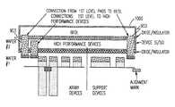
- FIG. 7shows a wafer at a stage of fabrication similar to that of FIG. 2A, described above and formed in substantially the same manner.
- FIG. 7differs from FIG. 2A by inclusion of support devices 701 and array devices 702 which can be formed on the same substrate by processes compatible with the formation of the memory cell array. Alignment marks 204 are provided as described above. Additionally, while connections within and between the array and support sections, it will generally be found convenient to provide connection pads 703 , 704 at the surface 705 of a planarized insulator (passivation) layer.
- an insulator/oxide 801is deposited and a SOI wafer is bonded thereto by processes such as those described above as shown in FIG. 9 .
- High performance devicescan then be formed on and/or in the SOI active layer and connections 901 formed to connection pads 703 (and/or 704 ) in the manner described above in connection with FIGS. 5 and 6. Connections may also be formed to other structures or connections in or on the bulk silicon wafer layer if desired.
- an additional oxide/insulator layer 902may be provided. If all desired circuit elements and connections have been formed and the device shown in FIG. 10 is substantially complete, such a layer serves as a passivation layer. If, however, even greater complexity and functionality is desired, oxide/insulator layer 902 can serve to bond another wafer 1000 thereto after formation of via connections to other connection pads 703 . This further wafer may be another SOI structure, a bare bulk silicon wafer or any other desired wafer structure.
- wafer or chip 1000includes devices which require heat treatment beyond that which can be withstood by the devices in wafer 900 , they can be fabricated on wafer or chip 1000 prior to bonding although accurate alignment for bonding will be required.
- the cost of such an alignment processis more than offset by the benefits of providing short connections to underlying chips and the ability to use technologies which may be incompatible with those on underlying wafers or chips.
- This process of laminating of chipscan be continued, at will and provides substantial design freedom as well as the capability to provide substantially unlimited integrated circuit complexity and functionality while supporting levels of performance not otherwise attainable by the short connections which can thus be provided.
Landscapes
- Engineering & Computer Science (AREA)
- Physics & Mathematics (AREA)
- Condensed Matter Physics & Semiconductors (AREA)
- General Physics & Mathematics (AREA)
- Computer Hardware Design (AREA)
- Microelectronics & Electronic Packaging (AREA)
- Power Engineering (AREA)
- Manufacturing & Machinery (AREA)
- Semiconductor Memories (AREA)
- Thin Film Transistor (AREA)
- Element Separation (AREA)
Abstract
Description
This application is a division of U.S. patent application Ser. No. 09/527,743 filed Mar. 17, 2000.
1. Field of the Invention
The present invention generally relates to semiconductor integrated circuits and, more particularly, to high capacity dynamic random access memories including high performance transistors in support circuitry thereof and other types of devices having differing circuit element requirements and to testing and burn-in thereof.
2. Description of the Prior Art
As the processing power of microprocessors has increased and cycle times reduced, higher capacity memories with more rapid access time have been demanded. Accordingly, dynamic memories have been developed with storage cells requiring reduced area or footprint such that memory chips having a capacity of a gigabit or more can be foreseen. Such storage cells are often formed by lining trenches in a chip of doped semiconductor with an insulator and filling the remainder of the trench with doped polysilicon to form an array of capacitors having a common electrode formed by the chip. A storage cell of such an array is generally referred to as a trench capacitor.
Substantial circuitry for accessing particular storage cells and sensing the charge stored therein is also required such as decoders, bit line drivers and sense amplifiers collectively referred to as “support circuits”. It is desirable and, at the present state of the art, substantially necessary to form support circuits on the same chip as the memory array. However, the support circuitry requires substantial chip area which is thus not available for formation of memory cells. Also, larger arrays imply longer word and bit lines which are necessarily of increased capacitance while storage cell size reduction tends to decrease capacitance of each storage cell. A reduction of the ratio of these capacitances reduces the voltage available to sense amplifiers and increases the criticality of sense amplifier operating margins.
Higher switching speeds and reduced cycle times have required new transistor technologies as well as high integration densities to reduce signal propagation time. At the present time, high performance transistors are often formed using silicon-on-insulator (SOI) technology because of the well-known device advantages of SOI such as reduced junction capacitance, latch-up immunity, improved isolation, steeper sub-Vt slope, reduced back-bias sensitivity and the like. Transistors fabricated using SOI technology provide particularly low power dissipation and high speed operation at low voltages (e.g. less than 1.5 volts).
A SOI wafer will typically comprise a relatively thin layer of silicon formed on an insulator which is, in turn supported by a bulk silicon wafer in order to withstand processing to form the active devices. The bulk silicon wafer has no electrical function and is fully insulated from any active devices which may be formed. SOI wafers may be formed in different ways including lamination of oxide-covered substrates oxide-to-oxide by heat treatment.
A leading process for constructing an SOI wafer is disclosed in “Smart Cut'; A Promising New SOI Material Technology” by M. Bruel et al.; Proceedings 1995 IEEE International SOI Conference; October, 1995, which is hereby fully incorporated by reference. This process includes the steps of implanting hydrogen into a first silicon wafer capped with oxide, room temperature hydrophilic bonding to a second wafer of bare silicon or oxide capped silicon, heat treatment of the bonded wafers at 400° C.-600° C. to cleave the wafers at a location within the silicon of the first wafer leaving the oxide cap(s) embedded and covered by a very thin layer of monocrystalline silicon from the first wafer bonded to and supported by the second wafer. The wafer is completed by a final chemical-mechanical polish step to reduce the surface roughness to a small fraction of a nanometer.
However, SOI transistors and trench capacitors are not compatible and cannot be easily integrated on the same chip. For example, voltages required for testing and burn-in of trench capacitors is greater than the breakdown voltage of the thin gate oxide of high performance field effect transistors. Further, the active device layer of SOI wafers is too thin to provide adequate capacitance at currently feasible minimum lithographic feature sizes and forming a trench through the insulator of an SOI wafer or chip would compromise the electrical isolation thereof. Moreover, the thermal budget required to form trench capacitors and node interconnections greatly exceeds the desired heat budget for forming high speed, low voltage logic switching devices in SOI.
Another problem involving on-chip capacitances required in increasing numbers of types of integrated circuits is the decoupling capacitance which is required in logic circuits operating at low voltage and clock frequencies greater than about 400 MHz to prevent unacceptable levels of switching noise (relative to the operating voltage) from being propagated through power connections. The intrachip area required for a planar capacitor is so large that multiple power supplies to reduce power/performance trade-offs cannot be included on the chip since the voltage regulators cannot be adequately decoupled with the capacitors which can be provided.
Incompatible technologies have been functionally reconciled to a degree by separately forming respective circuits on semiconductor substrates by different processes and bonding the respective substrates together to form a unitary chip. Many different structures have been used for this purpose including the stacking of chips. However, when chips are stacked, interchip connections other than at edges of the chips cannot be reliably formed at minimum lithography feature size and the available area of the edges limits the number of connections which can be made. By the same token, interchip connection pitches cannot approach the fineness of intrachip connection pitches. For both of these reasons, the number of interchip connections that can be reliably formed and used is very limited and is certainly insufficient for memory capacities which can be foreseen. Connections at the edges of chips are also not optimally short to limit signal propagation time.
Accordingly, there has been no solution to providing transistors of improved performance on the same chip with trench capacitor arrays while the need for faster access time and larger numbers of storage cells and high speed logic for accessing them has not been fully answered using technologies which are compatible with each other or incompatible technologies on separately processed, commonly packaged chips. Therefore, the current state of the art does not support significant further increases in either memory capacity or performance and requires substantial processing to both align the chip faces and seal the interchip wiring from external atmosphere which could cause deterioration thereof.
It is therefore an object of the present invention to provide a single chip having both a large array of trench capacitors and high performance SOI field effect transistors in support circuits.
It is another object of the invention to provide structures allowing large trench decoupling capacitors in combination with an SOI chip.
It is yet another object of the invention to provide a layered semiconductor chip utilizing different device technologies in respective layers.
It is a further object of the invention to provide a layered semiconductor chip where the length of connections between devices in respective layers can be minimized and provided over any or all regions of the chip.
It is yet another object of the invention to provide a novel technique of laminating semiconductor chips where circuit elements have been formed on at least one of the chips at the time of lamination.
It is another further object of the invention to provide a technique of forming a semiconductor integrated circuit device in which arbitrary circuit elements can be formed consistent with a restricted heat budget for gate oxides of high performance field effect transistors.
It is yet another object of the invention to provide interchip connections at fine pitch and which are lithographically defined.
In order to accomplish these and other objects of the invention, a structure of semiconductor material is provided including a silicon layer, an insulator layer on a major surface of the silicon layer, and a monocrystalline layer overlying the insulator layer; the silicon layer and the monocrystalline layer having integrated circuit elements formed therein. Essentially, the invention provide a SOI structure with integrated circuit elements formed in the “handle” layer.
In accordance with another aspect of the invention, a method of forming a semiconductor integrated circuit is provided comprising steps of forming integrated circuit elements in a first wafer, forming an oxide layer over the circuit elements, bonding a second wafer to the oxide layer, forming integrated circuit elements at a surface of the second wafer, and forming connections from the integrated circuit elements in the second wafer to the integrated circuit elements in the first wafer. In this way, interchip connections between wafers can be lithographically defined and reliably formed in much increased numbers at pitches similar to intrachip connection pitches.
In accordance with a further aspect of the invention, a method of providing power to logic circuits formed on an SOI wafer is provided including steps of forming decoupling capacitors in a bulk silicon wafer, bonding said SOI wafer to said bulk silicon wafer, and forming lithographically defined connections between said decoupling capacitors and circuit.
The foregoing and other objects, aspects and advantages will be better understood from the following detailed description of a preferred embodiment of the invention with reference to the drawings, in which:
FIGS. 1,2A,2B,3,4,5 and6 are a sequence of cross-sectional views illustrating fabrication a first embodiment of the invention, and
FIGS. 7,8,9,10 and11 are a sequence of cross-sectional views illustrating fabrication a second embodiment of the invention.
Referring now to the drawings, and more particularly to FIG. 1, there is shown, in cross-sectional view, abulk silicon wafer 100, preferably of the p− type. However, it should be understood that the conductivity types of impurities are not important to the principles of the invention or the types of circuit elements integrated therein to which the invention may be applied. That is, while the invention clearly has particular applicability to dynamic memories with respect to which it will be explained and for which the illustrated conductivities are preferred, the invention is more generally directed to the formation of composite, layered, chips with optimally short and reliably formed interconnections therebetween which are lithographically defined at pitches comparable to intra chip connections while incorporating incompatible technologies.
For purposes of forming a dynamic memory array, a deep n+ implantation is performed to create a thickconductive plate layer 120 while leaving a p−region 110 and ajunction 130 below it. The wafer is then annealed to remove all implant damage and a thin, high quality oxide layer is grown, followed by an oxide deposition. This oxide sequence forms a layer to be used as a hard mask for deep trench formation and for later bonding of a SOI wafer. The oxide is then patterned in any conventional manner to form the hard mask. At any convenient point in this process, alignment marks204 are applied for later use.
Then, as shown in FIG. 2A,deep trenches 201 are formed, preferably using the hard mask and reactive ion etching (RIE), and a capacitor dielectric202 (e.g. grown oxide, ONO or the like) is formed to line the trenches forming the memory cell array. A photoresist block-out mask is then applied and the dielectric removed from selected deep trenches which will form capacitor plate connections where desired. The block-out mask is then removed and doped polysilicon is deposited to fill the trenches and then planarized back by polishing to theinsulator 205 which also serves as a polish stop and to separate the storage nodes from the polysilicon plate interconnect(s) to thus form a dynamic storage capacitor array.
It should be appreciated that large numbers of capacitors of similar structure could be connected in parallel or other capacitor structures formed by use of the same sort of process to develop a number of capacitors of large value and suitable for decoupling capacitors or other purposes. Any portion or the entirety of the chip may be utilized for such capacitors. In the case of providing decoupling capacitors for multiple low voltage power supplies, it may be desirable to place the voltage regulators on the chip, as well.
It should also be appreciated that many other or alternative processes could be used to form a memory array or other forms of capacitors and the above processes should be regarded as exemplary and non-critical to the practice of the invention. For example, additional patterning of theinsulator layer 205 could be performed and metal or polysilicon damascene interconnects could also be formed therein. Other processes to optimize the storage capacitor structure or form isolation structures could also be included.
Also, as shown in FIG. 2B,temporary interconnects
FIG. 3 shows an SOI wafer having anactive region 301 andinsulator 302 as may be formed by, for example, the “Smart Cut” process alluded to above or any of a variety of other methods which will be apparent to those skilled in the art, such as SIMOX (an acronym for separation by implanted oxygen) or BESOI (an acronym for bond and etch back SOI) processes. “Smart Cut” processes are preferred since the wafer processed as described above could be a by-product of that process when the SOI wafer is cleaved therefrom. (The orientation ofSOI wafer 300 as shown in FIG. 3 is inverted from the orientation in which it would have been cleaved fromwafer 100 of FIG.1 and further oxidation oflayer 302 would have been performed. FIG. 4 shows this SOI wafer bonded to the integrated circuit structure of FIG. 2A atinterface 401.
The SOI wafer of FIG. 3 can be prepared in situ on the bulk silicon wafer in accordance with the “Smart Cut” process. In this case, a second wafer is implanted with hydrogen and an oxide is deposited and/or grown thereon and bonded to theoxide layer 205 of the wafer of FIG.2A. Upon low temperature heat treatment, the second wafer is cleaved in accordance with the “Smart Cut” process, leaving a thin monocrystalline silicon layer on thecomposite oxide layer
As shown in FIG. 5, standard transistor fabrication may now be performed on the SOI active layer in accordance with alignment marks204. For example,gate oxide regions 501 are grown and patterned andgate electrodes 502, preferably but optionally capped with nitride (to provide a borderless bit line contact) are applied.Sidewall spacers 503 may then be added in a self-aligned fashion. Severalactive regions insulation regions 507 are also formed by processes which will be evident to those skilled in the art, particularly to surround capacitor plate connections which are advantageously enhanced bydiffusion 506 during the heat treatment of the bonding process. The area of the trench capacitors is not limited, as shown in FIG. 5, since the capacitors are formed independently of the SOI layer, as described above, and may extend laterally under the MOSFETs even if the capacitors are storage capacitors for memory cells. Such an increase in lateral dimensions may reduce criticality of alignment during bonding, as well as providing the potential for increased memory cell storage capacitance.
It should also be noted that the interchip connection pitch to these capacitors and other circuits on the bulk wafer from the SOI wafer are lithographically defined and can be at pitches comparable to the intrachip connections on the SOI chip, allowing the number of interchip connections to be greatly increased. In addition, the number of interchip connections can be greatly increased, such connections may be utilized to partition the memory array more effectively to reduce bit line and word line length and capacitance; increasing operating margins of the memory (especially at the sense amplifiers) and/or reducing the required minimum operating voltage. Increased numbers of interchip connections also allow for sufficient numbers of them to be used for low resistance power supply connections and reduction of the need for larger connections to be provided.
Then, as shown in FIG. 6, the composite, layered, chip is completed by patterning the SOI wafer and insulators formed thereon to thedeep trench structures 203 and formingconductors connection 601. The plate connection is also a via formed by part ofconnection 602. Surface array connections such as word lines are provided byconnections 603 to the transistors.
A second embodiment of the invention will now be described with reference to FIGS. 7-11. FIG. 7 shows a wafer at a stage of fabrication similar to that of FIG. 2A, described above and formed in substantially the same manner. However, FIG. 7 differs from FIG. 2A by inclusion ofsupport devices 701 andarray devices 702 which can be formed on the same substrate by processes compatible with the formation of the memory cell array. Alignment marks204 are provided as described above. Additionally, while connections within and between the array and support sections, it will generally be found convenient to provideconnection pads surface 705 of a planarized insulator (passivation) layer.
As shown in FIG. 8, an insulator/oxide 801 is deposited and a SOI wafer is bonded thereto by processes such as those described above as shown in FIG.9. High performance devices can then be formed on and/or in the SOI active layer andconnections 901 formed to connection pads703 (and/or704) in the manner described above in connection with FIGS. 5 and 6. Connections may also be formed to other structures or connections in or on the bulk silicon wafer layer if desired.
Optionally, an additional oxide/insulator layer 902 may be provided. If all desired circuit elements and connections have been formed and the device shown in FIG. 10 is substantially complete, such a layer serves as a passivation layer. If, however, even greater complexity and functionality is desired, oxide/insulator layer 902 can serve to bond anotherwafer 1000 thereto after formation of via connections toother connection pads 703. This further wafer may be another SOI structure, a bare bulk silicon wafer or any other desired wafer structure.
If wafer orchip 1000 includes devices which require heat treatment beyond that which can be withstood by the devices inwafer 900, they can be fabricated on wafer orchip 1000 prior to bonding although accurate alignment for bonding will be required. However, the cost of such an alignment process is more than offset by the benefits of providing short connections to underlying chips and the ability to use technologies which may be incompatible with those on underlying wafers or chips. This process of laminating of chips can be continued, at will and provides substantial design freedom as well as the capability to provide substantially unlimited integrated circuit complexity and functionality while supporting levels of performance not otherwise attainable by the short connections which can thus be provided.
While the invention has been described in terms of a single preferred embodiment, those skilled in the art will recognize that the invention can be practiced with modification within the spirit and scope of the appended claims.
Claims (12)
1. A structure of semiconductor material including
a silicon layer,
an insulator layer on a major surface of said silicon layer, and
a monocrystalline layer overlying said insulator layer,
said silicon layer and said monocrystalline layer having integrated circuit elements formed therein, said integrated circuit elements being interconnected by a first interconnect structure overlaying said monocrystalline layer;
a second interconnect structure extending from said silicon layer through said insulator layer to electrically couple integrated circuit elements on said silicon layer to integrated circuit elements on said monocrystalline layer; and
a third interconnect structure extending from said silicon layer through said insulator layer and said monocrystalline layer to said interconnect structure, to electrically couple integrated circuit elements on said silicon layer to said first interconnect structure.
2. A structure as recited inclaim 1 , wherein said integrated circuit elements include memory cell capacitors.
3. A structure as recited inclaim 2 , wherein said integrated circuit elements further include word lines or bit lines.
4. A structure as recited inclaim 1 , wherein said integrated circuit elements include decoupling capacitors.
5. A structure as recited inclaim 4 , wherein said integrated circuit elements include voltage regulator circuits.
6. A structure as recited inclaim 1 ,
wherein said first conductive structure comprises a plurality of intrachip connections overlying said monocrystalline silicon layer; and
wherein said second conductive structure comprises a plurality of interchip connections located between active elements formed on said monocrystalline silicon layer, whereby at least some of said intra chip connections and some of said interchip connections are lithographically defined at similar pitches.
7. An integrated circuit, comprising
first and second semiconductor layers vertically separated an insulator structure;
a plurality of vertically-oriented storage nodes disposed on said first semiconductor layer;
a plurality of array transistors disposed on said second semiconductor layer having gate structures at least partially extending over said vertically oriented storage nodes, at least some of adjacent ones of said gate structures being separated from one another by a given space; and
a conductive interconnect disposed in each given space and extending through said second semiconductor layers to form contacts between an abutting one of said array transistors and a respective one of said vertically-oriented storage nodes, and further comprising a plurality of high performance support devices disposed on said second semiconductor layer and not overlapping said plurality of vertically-oriented storage nodes.
8. The integrated circuit ofclaim 7 , further comprising a second insulator layer on said second semiconductor layer and a third semiconductor layer on said second insulator layer.
9. The integrated circuit ofclaim 8 , wherein a plurality of high performance devices are disposed on said third semiconductor layer.
10. The integrated circuit ofclaim 9 , wherein a first interconnect structure is disposed on said third semiconductor layer.
11. The integrated circuit ofclaim 10 , further comprising a second interconnect structure that extends from said first semiconductor layer through said first insulator layer, said second semiconductor layer, and said second insulator layer into said third semiconductor layer to interconnect given ones of said plurality of array transistors to given ones of said high performance devices.
12. The integrated circuit ofclaim 10 , further comprising a third interconnect structure that extends from said first semiconductor layer, through said first insulator layer, said second semiconductor layer, said second insulator layer, and said third semiconductor layer, to interconnect given ones of said plurality of array transistors to said first interconnect structure.
Priority Applications (1)
| Application Number | Priority Date | Filing Date | Title |
|---|---|---|---|
| US09/998,318US6590258B2 (en) | 2000-03-17 | 2001-12-03 | SIO stacked DRAM logic |
Applications Claiming Priority (2)
| Application Number | Priority Date | Filing Date | Title |
|---|---|---|---|
| US09/527,743US6544837B1 (en) | 2000-03-17 | 2000-03-17 | SOI stacked DRAM logic |
| US09/998,318US6590258B2 (en) | 2000-03-17 | 2001-12-03 | SIO stacked DRAM logic |
Related Parent Applications (1)
| Application Number | Title | Priority Date | Filing Date |
|---|---|---|---|
| US09/527,743DivisionUS6544837B1 (en) | 2000-03-17 | 2000-03-17 | SOI stacked DRAM logic |
Publications (2)
| Publication Number | Publication Date |
|---|---|
| US20020036322A1 US20020036322A1 (en) | 2002-03-28 |
| US6590258B2true US6590258B2 (en) | 2003-07-08 |
Family
ID=24102747
Family Applications (2)
| Application Number | Title | Priority Date | Filing Date |
|---|---|---|---|
| US09/527,743Expired - Fee RelatedUS6544837B1 (en) | 2000-03-17 | 2000-03-17 | SOI stacked DRAM logic |
| US09/998,318Expired - Fee RelatedUS6590258B2 (en) | 2000-03-17 | 2001-12-03 | SIO stacked DRAM logic |
Family Applications Before (1)
| Application Number | Title | Priority Date | Filing Date |
|---|---|---|---|
| US09/527,743Expired - Fee RelatedUS6544837B1 (en) | 2000-03-17 | 2000-03-17 | SOI stacked DRAM logic |
Country Status (1)
| Country | Link |
|---|---|
| US (2) | US6544837B1 (en) |
Cited By (66)
| Publication number | Priority date | Publication date | Assignee | Title |
|---|---|---|---|---|
| US20040021137A1 (en)* | 2001-06-18 | 2004-02-05 | Pierre Fazan | Semiconductor device |
| US20040227166A1 (en)* | 2003-05-13 | 2004-11-18 | Lionel Portmann | Reference current generator, and method of programming, adjusting and/or operating same |
| US20040228168A1 (en)* | 2003-05-13 | 2004-11-18 | Richard Ferrant | Semiconductor memory device and method of operating same |
| US20040238890A1 (en)* | 2002-04-18 | 2004-12-02 | Pierre Fazan | Semiconductor device |
| US20040240306A1 (en)* | 2002-04-18 | 2004-12-02 | Pierre Fazan | Data storage device and refreshing method for use with such device |
| US20050013163A1 (en)* | 2003-05-13 | 2005-01-20 | Richard Ferrant | Semiconductor memory cell, array, architecture and device, and method of operating same |
| US20050017240A1 (en)* | 2003-07-22 | 2005-01-27 | Pierre Fazan | Integrated circuit device, and method of fabricating same |
| US20050063224A1 (en)* | 2003-09-24 | 2005-03-24 | Pierre Fazan | Low power programming technique for a floating body memory transistor, memory cell, and memory array |
| US20050121722A1 (en)* | 2001-12-25 | 2005-06-09 | Hisato Oyamatsu | Semiconductor device having patterned SOI structure and method for fabricating the same |
| US20050146565A1 (en)* | 2002-04-15 | 2005-07-07 | Emery Timothy R. | Bonding structure and method of making |
| US20060091462A1 (en)* | 2004-11-04 | 2006-05-04 | Serguei Okhonin | Memory cell having an electrically floating body transistor and programming technique therefor |
| US20060098481A1 (en)* | 2004-11-10 | 2006-05-11 | Serguei Okhonin | Circuitry for and method of improving statistical distribution of integrated circuits |
| US20060126374A1 (en)* | 2004-12-13 | 2006-06-15 | Waller William K | Sense amplifier circuitry and architecture to write data into and/or read from memory cells |
| US20060131650A1 (en)* | 2004-12-22 | 2006-06-22 | Serguei Okhonin | Bipolar reading technique for a memory cell having an electrically floating body transistor |
| US20060226491A1 (en)* | 2005-04-06 | 2006-10-12 | International Business Machines Corporation | Inverted multilayer semiconductor device assembly |
| US20070023833A1 (en)* | 2005-07-28 | 2007-02-01 | Serguei Okhonin | Method for reading a memory cell having an electrically floating body transistor, and memory cell and array implementing same |
| US20070058427A1 (en)* | 2005-09-07 | 2007-03-15 | Serguei Okhonin | Memory cell and memory cell array having an electrically floating body transistor, and methods of operating same |
| US20070064489A1 (en)* | 2005-09-19 | 2007-03-22 | Philippe Bauser | Method and circuitry to generate a reference current for reading a memory cell, and device implementing same |
| US20070085140A1 (en)* | 2005-10-19 | 2007-04-19 | Cedric Bassin | One transistor memory cell having strained electrically floating body region, and method of operating same |
| US20070138530A1 (en)* | 2005-12-19 | 2007-06-21 | Serguei Okhonin | Electrically floating body memory cell and array, and method of operating or controlling same |
| US20070187775A1 (en)* | 2006-02-16 | 2007-08-16 | Serguei Okhonin | Multi-bit memory cell having electrically floating body transistor, and method of programming and reading same |
| US7492632B2 (en) | 2006-04-07 | 2009-02-17 | Innovative Silicon Isi Sa | Memory array having a programmable word length, and method of operating same |
| US7542340B2 (en) | 2006-07-11 | 2009-06-02 | Innovative Silicon Isi Sa | Integrated circuit including memory array having a segmented bit line architecture and method of controlling and/or operating same |
| US7606098B2 (en) | 2006-04-18 | 2009-10-20 | Innovative Silicon Isi Sa | Semiconductor memory array architecture with grouped memory cells, and method of controlling same |
| US20100083999A1 (en)* | 2008-10-01 | 2010-04-08 | International Business Machines Corporation | Tandem nanofilm solar cells joined by wafer bonding |
| US7924630B2 (en) | 2008-10-15 | 2011-04-12 | Micron Technology, Inc. | Techniques for simultaneously driving a plurality of source lines |
| US7927975B2 (en) | 2009-02-04 | 2011-04-19 | Micron Technology, Inc. | Semiconductor material manufacture |
| US7933142B2 (en) | 2006-05-02 | 2011-04-26 | Micron Technology, Inc. | Semiconductor memory cell and array using punch-through to program and read same |
| US7933140B2 (en) | 2008-10-02 | 2011-04-26 | Micron Technology, Inc. | Techniques for reducing a voltage swing |
| US7947543B2 (en) | 2008-09-25 | 2011-05-24 | Micron Technology, Inc. | Recessed gate silicon-on-insulator floating body device with self-aligned lateral isolation |
| US7957206B2 (en) | 2008-04-04 | 2011-06-07 | Micron Technology, Inc. | Read circuitry for an integrated circuit having memory cells and/or a memory cell array, and method of operating same |
| US20110204524A1 (en)* | 2010-02-23 | 2011-08-25 | International Business Machines Corporation | Structures and methods of forming pre fabricated deep trench capacitors for soi substrates |
| US8014195B2 (en) | 2008-02-06 | 2011-09-06 | Micron Technology, Inc. | Single transistor memory cell |
| US8064274B2 (en) | 2007-05-30 | 2011-11-22 | Micron Technology, Inc. | Integrated circuit having voltage generation circuitry for memory cell array, and method of operating and/or controlling same |
| US8069377B2 (en) | 2006-06-26 | 2011-11-29 | Micron Technology, Inc. | Integrated circuit having memory array including ECC and column redundancy and method of operating the same |
| US8085594B2 (en) | 2007-06-01 | 2011-12-27 | Micron Technology, Inc. | Reading technique for memory cell with electrically floating body transistor |
| US8139418B2 (en) | 2009-04-27 | 2012-03-20 | Micron Technology, Inc. | Techniques for controlling a direct injection semiconductor memory device |
| US8174881B2 (en) | 2009-11-24 | 2012-05-08 | Micron Technology, Inc. | Techniques for reducing disturbance in a semiconductor device |
| US8189376B2 (en) | 2008-02-08 | 2012-05-29 | Micron Technology, Inc. | Integrated circuit having memory cells including gate material having high work function, and method of manufacturing same |
| US8194487B2 (en) | 2007-09-17 | 2012-06-05 | Micron Technology, Inc. | Refreshing data of memory cells with electrically floating body transistors |
| US8199595B2 (en) | 2009-09-04 | 2012-06-12 | Micron Technology, Inc. | Techniques for sensing a semiconductor memory device |
| US8213226B2 (en) | 2008-12-05 | 2012-07-03 | Micron Technology, Inc. | Vertical transistor memory cell and array |
| US8223574B2 (en) | 2008-11-05 | 2012-07-17 | Micron Technology, Inc. | Techniques for block refreshing a semiconductor memory device |
| US8264041B2 (en) | 2007-01-26 | 2012-09-11 | Micron Technology, Inc. | Semiconductor device with electrically floating body |
| US8310893B2 (en) | 2009-12-16 | 2012-11-13 | Micron Technology, Inc. | Techniques for reducing impact of array disturbs in a semiconductor memory device |
| US8315099B2 (en) | 2009-07-27 | 2012-11-20 | Micron Technology, Inc. | Techniques for providing a direct injection semiconductor memory device |
| US8319294B2 (en) | 2009-02-18 | 2012-11-27 | Micron Technology, Inc. | Techniques for providing a source line plane |
| US8349662B2 (en) | 2007-12-11 | 2013-01-08 | Micron Technology, Inc. | Integrated circuit having memory cell array, and method of manufacturing same |
| US8369177B2 (en) | 2010-03-05 | 2013-02-05 | Micron Technology, Inc. | Techniques for reading from and/or writing to a semiconductor memory device |
| US8411513B2 (en) | 2010-03-04 | 2013-04-02 | Micron Technology, Inc. | Techniques for providing a semiconductor memory device having hierarchical bit lines |
| US8411524B2 (en) | 2010-05-06 | 2013-04-02 | Micron Technology, Inc. | Techniques for refreshing a semiconductor memory device |
| US8416636B2 (en) | 2010-02-12 | 2013-04-09 | Micron Technology, Inc. | Techniques for controlling a semiconductor memory device |
| US8498157B2 (en) | 2009-05-22 | 2013-07-30 | Micron Technology, Inc. | Techniques for providing a direct injection semiconductor memory device |
| US8508994B2 (en) | 2009-04-30 | 2013-08-13 | Micron Technology, Inc. | Semiconductor device with floating gate and electrically floating body |
| US8518774B2 (en) | 2007-03-29 | 2013-08-27 | Micron Technology, Inc. | Manufacturing process for zero-capacitor random access memory circuits |
| US8531878B2 (en) | 2011-05-17 | 2013-09-10 | Micron Technology, Inc. | Techniques for providing a semiconductor memory device |
| US8536628B2 (en) | 2007-11-29 | 2013-09-17 | Micron Technology, Inc. | Integrated circuit having memory cell array including barriers, and method of manufacturing same |
| US8537610B2 (en) | 2009-07-10 | 2013-09-17 | Micron Technology, Inc. | Techniques for providing a semiconductor memory device |
| US8546961B2 (en) | 2011-01-10 | 2013-10-01 | International Business Machines Corporation | Alignment marks to enable 3D integration |
| US8547738B2 (en) | 2010-03-15 | 2013-10-01 | Micron Technology, Inc. | Techniques for providing a semiconductor memory device |
| US8576631B2 (en) | 2010-03-04 | 2013-11-05 | Micron Technology, Inc. | Techniques for sensing a semiconductor memory device |
| US8710566B2 (en) | 2009-03-04 | 2014-04-29 | Micron Technology, Inc. | Techniques for forming a contact to a buried diffusion layer in a semiconductor memory device |
| US8748959B2 (en) | 2009-03-31 | 2014-06-10 | Micron Technology, Inc. | Semiconductor memory device |
| US8773933B2 (en) | 2012-03-16 | 2014-07-08 | Micron Technology, Inc. | Techniques for accessing memory cells |
| US9559216B2 (en) | 2011-06-06 | 2017-01-31 | Micron Technology, Inc. | Semiconductor memory device and method for biasing same |
| US20170373003A1 (en)* | 2016-06-22 | 2017-12-28 | Nanya Technology Corporation | Semiconductor chip and multi-chip package using thereof |
Families Citing this family (235)
| Publication number | Priority date | Publication date | Assignee | Title |
|---|---|---|---|---|
| TW540154B (en)* | 2001-06-04 | 2003-07-01 | Promos Technologies Inc | Deep trench capacitor structure and its manufacturing method |
| US7102204B2 (en)* | 2004-06-29 | 2006-09-05 | International Business Machines Corporation | Integrated SOI fingered decoupling capacitor |
| US7348658B2 (en)* | 2004-08-30 | 2008-03-25 | International Business Machines Corporation | Multilayer silicon over insulator device |
| US7229877B2 (en)* | 2004-11-17 | 2007-06-12 | International Business Machines Corporation | Trench capacitor with hybrid surface orientation substrate |
| JP2008153411A (en)* | 2006-12-18 | 2008-07-03 | Shin Etsu Chem Co Ltd | Manufacturing method of SOI substrate |
| US8378715B2 (en) | 2009-04-14 | 2013-02-19 | Monolithic 3D Inc. | Method to construct systems |
| US8669778B1 (en) | 2009-04-14 | 2014-03-11 | Monolithic 3D Inc. | Method for design and manufacturing of a 3D semiconductor device |
| US8384426B2 (en) | 2009-04-14 | 2013-02-26 | Monolithic 3D Inc. | Semiconductor device and structure |
| US8754533B2 (en) | 2009-04-14 | 2014-06-17 | Monolithic 3D Inc. | Monolithic three-dimensional semiconductor device and structure |
| US9711407B2 (en) | 2009-04-14 | 2017-07-18 | Monolithic 3D Inc. | Method of manufacturing a three dimensional integrated circuit by transfer of a mono-crystalline layer |
| US8362482B2 (en) | 2009-04-14 | 2013-01-29 | Monolithic 3D Inc. | Semiconductor device and structure |
| US8258810B2 (en) | 2010-09-30 | 2012-09-04 | Monolithic 3D Inc. | 3D semiconductor device |
| US9509313B2 (en) | 2009-04-14 | 2016-11-29 | Monolithic 3D Inc. | 3D semiconductor device |
| US8058137B1 (en) | 2009-04-14 | 2011-11-15 | Monolithic 3D Inc. | Method for fabrication of a semiconductor device and structure |
| US8405420B2 (en) | 2009-04-14 | 2013-03-26 | Monolithic 3D Inc. | System comprising a semiconductor device and structure |
| US9577642B2 (en) | 2009-04-14 | 2017-02-21 | Monolithic 3D Inc. | Method to form a 3D semiconductor device |
| US8427200B2 (en) | 2009-04-14 | 2013-04-23 | Monolithic 3D Inc. | 3D semiconductor device |
| US7986042B2 (en) | 2009-04-14 | 2011-07-26 | Monolithic 3D Inc. | Method for fabrication of a semiconductor device and structure |
| US8362800B2 (en) | 2010-10-13 | 2013-01-29 | Monolithic 3D Inc. | 3D semiconductor device including field repairable logics |
| US8373439B2 (en) | 2009-04-14 | 2013-02-12 | Monolithic 3D Inc. | 3D semiconductor device |
| US8395191B2 (en) | 2009-10-12 | 2013-03-12 | Monolithic 3D Inc. | Semiconductor device and structure |
| US8021941B2 (en)* | 2009-07-21 | 2011-09-20 | International Business Machines Corporation | Bias-controlled deep trench substrate noise isolation integrated circuit device structures |
| FR2950734B1 (en)* | 2009-09-28 | 2011-12-09 | Soitec Silicon On Insulator | METHOD FOR BONDING AND TRANSFERRING A LAYER |
| US8476145B2 (en) | 2010-10-13 | 2013-07-02 | Monolithic 3D Inc. | Method of fabricating a semiconductor device and structure |
| US11984445B2 (en) | 2009-10-12 | 2024-05-14 | Monolithic 3D Inc. | 3D semiconductor devices and structures with metal layers |
| US10354995B2 (en) | 2009-10-12 | 2019-07-16 | Monolithic 3D Inc. | Semiconductor memory device and structure |
| US8536023B2 (en) | 2010-11-22 | 2013-09-17 | Monolithic 3D Inc. | Method of manufacturing a semiconductor device and structure |
| US10910364B2 (en) | 2009-10-12 | 2021-02-02 | Monolitaic 3D Inc. | 3D semiconductor device |
| US8742476B1 (en) | 2012-11-27 | 2014-06-03 | Monolithic 3D Inc. | Semiconductor device and structure |
| US10043781B2 (en) | 2009-10-12 | 2018-08-07 | Monolithic 3D Inc. | 3D semiconductor device and structure |
| US8148728B2 (en) | 2009-10-12 | 2012-04-03 | Monolithic 3D, Inc. | Method for fabrication of a semiconductor device and structure |
| US12027518B1 (en) | 2009-10-12 | 2024-07-02 | Monolithic 3D Inc. | 3D semiconductor devices and structures with metal layers |
| US9099424B1 (en) | 2012-08-10 | 2015-08-04 | Monolithic 3D Inc. | Semiconductor system, device and structure with heat removal |
| US10366970B2 (en) | 2009-10-12 | 2019-07-30 | Monolithic 3D Inc. | 3D semiconductor device and structure |
| US8581349B1 (en) | 2011-05-02 | 2013-11-12 | Monolithic 3D Inc. | 3D memory semiconductor device and structure |
| US11374118B2 (en) | 2009-10-12 | 2022-06-28 | Monolithic 3D Inc. | Method to form a 3D integrated circuit |
| US10157909B2 (en) | 2009-10-12 | 2018-12-18 | Monolithic 3D Inc. | 3D semiconductor device and structure |
| US10388863B2 (en) | 2009-10-12 | 2019-08-20 | Monolithic 3D Inc. | 3D memory device and structure |
| US8450804B2 (en) | 2011-03-06 | 2013-05-28 | Monolithic 3D Inc. | Semiconductor device and structure for heat removal |
| US11018133B2 (en) | 2009-10-12 | 2021-05-25 | Monolithic 3D Inc. | 3D integrated circuit |
| KR101576296B1 (en)* | 2009-12-11 | 2015-12-10 | 주식회사 동부하이텍 | Capcitor for semiconductor device and manufacturing method of capacitor for semiconductor device |
| US8373230B1 (en) | 2010-10-13 | 2013-02-12 | Monolithic 3D Inc. | Method for fabrication of a semiconductor device and structure |
| US8461035B1 (en) | 2010-09-30 | 2013-06-11 | Monolithic 3D Inc. | Method for fabrication of a semiconductor device and structure |
| US8492886B2 (en) | 2010-02-16 | 2013-07-23 | Monolithic 3D Inc | 3D integrated circuit with logic |
| US8026521B1 (en) | 2010-10-11 | 2011-09-27 | Monolithic 3D Inc. | Semiconductor device and structure |
| US9099526B2 (en) | 2010-02-16 | 2015-08-04 | Monolithic 3D Inc. | Integrated circuit device and structure |
| US8298875B1 (en) | 2011-03-06 | 2012-10-30 | Monolithic 3D Inc. | Method for fabrication of a semiconductor device and structure |
| US8541819B1 (en) | 2010-12-09 | 2013-09-24 | Monolithic 3D Inc. | Semiconductor device and structure |
| US10217667B2 (en) | 2011-06-28 | 2019-02-26 | Monolithic 3D Inc. | 3D semiconductor device, fabrication method and system |
| US9953925B2 (en) | 2011-06-28 | 2018-04-24 | Monolithic 3D Inc. | Semiconductor system and device |
| US9219005B2 (en) | 2011-06-28 | 2015-12-22 | Monolithic 3D Inc. | Semiconductor system and device |
| US8642416B2 (en) | 2010-07-30 | 2014-02-04 | Monolithic 3D Inc. | Method of forming three dimensional integrated circuit devices using layer transfer technique |
| US8901613B2 (en) | 2011-03-06 | 2014-12-02 | Monolithic 3D Inc. | Semiconductor device and structure for heat removal |
| US11482440B2 (en) | 2010-12-16 | 2022-10-25 | Monolithic 3D Inc. | 3D semiconductor device and structure with a built-in test circuit for repairing faulty circuits |
| US12362219B2 (en) | 2010-11-18 | 2025-07-15 | Monolithic 3D Inc. | 3D semiconductor memory device and structure |
| US8163581B1 (en) | 2010-10-13 | 2012-04-24 | Monolith IC 3D | Semiconductor and optoelectronic devices |
| US10497713B2 (en) | 2010-11-18 | 2019-12-03 | Monolithic 3D Inc. | 3D semiconductor memory device and structure |
| US8273610B2 (en) | 2010-11-18 | 2012-09-25 | Monolithic 3D Inc. | Method of constructing a semiconductor device and structure |
| US8114757B1 (en) | 2010-10-11 | 2012-02-14 | Monolithic 3D Inc. | Semiconductor device and structure |
| US11600667B1 (en) | 2010-10-11 | 2023-03-07 | Monolithic 3D Inc. | Method to produce 3D semiconductor devices and structures with memory |
| US11024673B1 (en) | 2010-10-11 | 2021-06-01 | Monolithic 3D Inc. | 3D semiconductor device and structure |
| US11018191B1 (en) | 2010-10-11 | 2021-05-25 | Monolithic 3D Inc. | 3D semiconductor device and structure |
| US11257867B1 (en) | 2010-10-11 | 2022-02-22 | Monolithic 3D Inc. | 3D semiconductor device and structure with oxide bonds |
| US11158674B2 (en) | 2010-10-11 | 2021-10-26 | Monolithic 3D Inc. | Method to produce a 3D semiconductor device and structure |
| US11469271B2 (en) | 2010-10-11 | 2022-10-11 | Monolithic 3D Inc. | Method to produce 3D semiconductor devices and structures with memory |
| US10896931B1 (en) | 2010-10-11 | 2021-01-19 | Monolithic 3D Inc. | 3D semiconductor device and structure |
| US11315980B1 (en) | 2010-10-11 | 2022-04-26 | Monolithic 3D Inc. | 3D semiconductor device and structure with transistors |
| US11227897B2 (en) | 2010-10-11 | 2022-01-18 | Monolithic 3D Inc. | Method for producing a 3D semiconductor memory device and structure |
| US10290682B2 (en) | 2010-10-11 | 2019-05-14 | Monolithic 3D Inc. | 3D IC semiconductor device and structure with stacked memory |
| US10978501B1 (en) | 2010-10-13 | 2021-04-13 | Monolithic 3D Inc. | Multilevel semiconductor device and structure with waveguides |
| US8283215B2 (en) | 2010-10-13 | 2012-10-09 | Monolithic 3D Inc. | Semiconductor and optoelectronic devices |
| US10679977B2 (en) | 2010-10-13 | 2020-06-09 | Monolithic 3D Inc. | 3D microdisplay device and structure |
| US11133344B2 (en) | 2010-10-13 | 2021-09-28 | Monolithic 3D Inc. | Multilevel semiconductor device and structure with image sensors |
| US11437368B2 (en) | 2010-10-13 | 2022-09-06 | Monolithic 3D Inc. | Multilevel semiconductor device and structure with oxide bonding |
| US11984438B2 (en) | 2010-10-13 | 2024-05-14 | Monolithic 3D Inc. | Multilevel semiconductor device and structure with oxide bonding |
| US11929372B2 (en) | 2010-10-13 | 2024-03-12 | Monolithic 3D Inc. | Multilevel semiconductor device and structure with image sensors and wafer bonding |
| US12360310B2 (en) | 2010-10-13 | 2025-07-15 | Monolithic 3D Inc. | Multilevel semiconductor device and structure with oxide bonding |
| US11327227B2 (en) | 2010-10-13 | 2022-05-10 | Monolithic 3D Inc. | Multilevel semiconductor device and structure with electromagnetic modulators |
| US11163112B2 (en) | 2010-10-13 | 2021-11-02 | Monolithic 3D Inc. | Multilevel semiconductor device and structure with electromagnetic modulators |
| US11605663B2 (en) | 2010-10-13 | 2023-03-14 | Monolithic 3D Inc. | Multilevel semiconductor device and structure with image sensors and wafer bonding |
| US11063071B1 (en) | 2010-10-13 | 2021-07-13 | Monolithic 3D Inc. | Multilevel semiconductor device and structure with waveguides |
| US10833108B2 (en) | 2010-10-13 | 2020-11-10 | Monolithic 3D Inc. | 3D microdisplay device and structure |
| US11855100B2 (en) | 2010-10-13 | 2023-12-26 | Monolithic 3D Inc. | Multilevel semiconductor device and structure with oxide bonding |
| US11694922B2 (en) | 2010-10-13 | 2023-07-04 | Monolithic 3D Inc. | Multilevel semiconductor device and structure with oxide bonding |
| US9197804B1 (en) | 2011-10-14 | 2015-11-24 | Monolithic 3D Inc. | Semiconductor and optoelectronic devices |
| US11164898B2 (en) | 2010-10-13 | 2021-11-02 | Monolithic 3D Inc. | Multilevel semiconductor device and structure |
| US10998374B1 (en) | 2010-10-13 | 2021-05-04 | Monolithic 3D Inc. | Multilevel semiconductor device and structure |
| US12094892B2 (en) | 2010-10-13 | 2024-09-17 | Monolithic 3D Inc. | 3D micro display device and structure |
| US11043523B1 (en) | 2010-10-13 | 2021-06-22 | Monolithic 3D Inc. | Multilevel semiconductor device and structure with image sensors |
| US11869915B2 (en) | 2010-10-13 | 2024-01-09 | Monolithic 3D Inc. | Multilevel semiconductor device and structure with image sensors and wafer bonding |
| US11404466B2 (en) | 2010-10-13 | 2022-08-02 | Monolithic 3D Inc. | Multilevel semiconductor device and structure with image sensors |
| US10943934B2 (en) | 2010-10-13 | 2021-03-09 | Monolithic 3D Inc. | Multilevel semiconductor device and structure |
| US11855114B2 (en) | 2010-10-13 | 2023-12-26 | Monolithic 3D Inc. | Multilevel semiconductor device and structure with image sensors and wafer bonding |
| US8379458B1 (en) | 2010-10-13 | 2013-02-19 | Monolithic 3D Inc. | Semiconductor device and structure |
| US12080743B2 (en) | 2010-10-13 | 2024-09-03 | Monolithic 3D Inc. | Multilevel semiconductor device and structure with image sensors and wafer bonding |
| US11610802B2 (en) | 2010-11-18 | 2023-03-21 | Monolithic 3D Inc. | Method for producing a 3D semiconductor device and structure with single crystal transistors and metal gate electrodes |
| US12154817B1 (en) | 2010-11-18 | 2024-11-26 | Monolithic 3D Inc. | Methods for producing a 3D semiconductor memory device and structure |
| US12144190B2 (en) | 2010-11-18 | 2024-11-12 | Monolithic 3D Inc. | 3D semiconductor device and structure with bonding and memory cells preliminary class |
| US11121021B2 (en) | 2010-11-18 | 2021-09-14 | Monolithic 3D Inc. | 3D semiconductor device and structure |
| US12068187B2 (en) | 2010-11-18 | 2024-08-20 | Monolithic 3D Inc. | 3D semiconductor device and structure with bonding and DRAM memory cells |
| US11482438B2 (en) | 2010-11-18 | 2022-10-25 | Monolithic 3D Inc. | Methods for producing a 3D semiconductor memory device and structure |
| US12243765B2 (en) | 2010-11-18 | 2025-03-04 | Monolithic 3D Inc. | 3D semiconductor device and structure with metal layers and memory cells |
| US11355380B2 (en) | 2010-11-18 | 2022-06-07 | Monolithic 3D Inc. | Methods for producing 3D semiconductor memory device and structure utilizing alignment marks |
| US11164770B1 (en) | 2010-11-18 | 2021-11-02 | Monolithic 3D Inc. | Method for producing a 3D semiconductor memory device and structure |
| US11804396B2 (en) | 2010-11-18 | 2023-10-31 | Monolithic 3D Inc. | Methods for producing a 3D semiconductor device and structure with memory cells and multiple metal layers |
| US11569117B2 (en) | 2010-11-18 | 2023-01-31 | Monolithic 3D Inc. | 3D semiconductor device and structure with single-crystal layers |
| US11901210B2 (en) | 2010-11-18 | 2024-02-13 | Monolithic 3D Inc. | 3D semiconductor device and structure with memory |
| US11854857B1 (en) | 2010-11-18 | 2023-12-26 | Monolithic 3D Inc. | Methods for producing a 3D semiconductor device and structure with memory cells and multiple metal layers |
| US11615977B2 (en) | 2010-11-18 | 2023-03-28 | Monolithic 3D Inc. | 3D semiconductor memory device and structure |
| US12272586B2 (en) | 2010-11-18 | 2025-04-08 | Monolithic 3D Inc. | 3D semiconductor memory device and structure with memory and metal layers |
| US11862503B2 (en) | 2010-11-18 | 2024-01-02 | Monolithic 3D Inc. | Method for producing a 3D semiconductor device and structure with memory cells and multiple metal layers |
| US11355381B2 (en) | 2010-11-18 | 2022-06-07 | Monolithic 3D Inc. | 3D semiconductor memory device and structure |
| US11521888B2 (en) | 2010-11-18 | 2022-12-06 | Monolithic 3D Inc. | 3D semiconductor device and structure with high-k metal gate transistors |
| US11923230B1 (en) | 2010-11-18 | 2024-03-05 | Monolithic 3D Inc. | 3D semiconductor device and structure with bonding |
| US11094576B1 (en) | 2010-11-18 | 2021-08-17 | Monolithic 3D Inc. | Methods for producing a 3D semiconductor memory device and structure |
| US11018042B1 (en) | 2010-11-18 | 2021-05-25 | Monolithic 3D Inc. | 3D semiconductor memory device and structure |
| US11443971B2 (en) | 2010-11-18 | 2022-09-13 | Monolithic 3D Inc. | 3D semiconductor device and structure with memory |
| US11495484B2 (en) | 2010-11-18 | 2022-11-08 | Monolithic 3D Inc. | 3D semiconductor devices and structures with at least two single-crystal layers |
| US12136562B2 (en) | 2010-11-18 | 2024-11-05 | Monolithic 3D Inc. | 3D semiconductor device and structure with single-crystal layers |
| US11031275B2 (en) | 2010-11-18 | 2021-06-08 | Monolithic 3D Inc. | 3D semiconductor device and structure with memory |
| US12125737B1 (en) | 2010-11-18 | 2024-10-22 | Monolithic 3D Inc. | 3D semiconductor device and structure with metal layers and memory cells |
| US12033884B2 (en) | 2010-11-18 | 2024-07-09 | Monolithic 3D Inc. | Methods for producing a 3D semiconductor device and structure with memory cells and multiple metal layers |
| US11735462B2 (en) | 2010-11-18 | 2023-08-22 | Monolithic 3D Inc. | 3D semiconductor device and structure with single-crystal layers |
| US11211279B2 (en) | 2010-11-18 | 2021-12-28 | Monolithic 3D Inc. | Method for processing a 3D integrated circuit and structure |
| US11107721B2 (en) | 2010-11-18 | 2021-08-31 | Monolithic 3D Inc. | 3D semiconductor device and structure with NAND logic |
| US12100611B2 (en) | 2010-11-18 | 2024-09-24 | Monolithic 3D Inc. | Methods for producing a 3D semiconductor device and structure with memory cells and multiple metal layers |
| US11784082B2 (en) | 2010-11-18 | 2023-10-10 | Monolithic 3D Inc. | 3D semiconductor device and structure with bonding |
| US11004719B1 (en) | 2010-11-18 | 2021-05-11 | Monolithic 3D Inc. | Methods for producing a 3D semiconductor memory device and structure |
| US11508605B2 (en) | 2010-11-18 | 2022-11-22 | Monolithic 3D Inc. | 3D semiconductor memory device and structure |
| US11482439B2 (en) | 2010-11-18 | 2022-10-25 | Monolithic 3D Inc. | Methods for producing a 3D semiconductor memory device comprising charge trap junction-less transistors |
| JP5737922B2 (en)* | 2010-12-14 | 2015-06-17 | ピーエスフォー ルクスコ エスエイアールエルPS4 Luxco S.a.r.l. | Manufacturing method of semiconductor device |
| US8975670B2 (en) | 2011-03-06 | 2015-03-10 | Monolithic 3D Inc. | Semiconductor device and structure for heat removal |
| US10388568B2 (en) | 2011-06-28 | 2019-08-20 | Monolithic 3D Inc. | 3D semiconductor device and system |
| US8687399B2 (en) | 2011-10-02 | 2014-04-01 | Monolithic 3D Inc. | Semiconductor device and structure |
| US9029173B2 (en) | 2011-10-18 | 2015-05-12 | Monolithic 3D Inc. | Method for fabrication of a semiconductor device and structure |
| US9000557B2 (en) | 2012-03-17 | 2015-04-07 | Zvi Or-Bach | Semiconductor device and structure |
| US11881443B2 (en) | 2012-04-09 | 2024-01-23 | Monolithic 3D Inc. | 3D semiconductor device and structure with metal layers and a connective path |
| US8557632B1 (en) | 2012-04-09 | 2013-10-15 | Monolithic 3D Inc. | Method for fabrication of a semiconductor device and structure |
| US11594473B2 (en) | 2012-04-09 | 2023-02-28 | Monolithic 3D Inc. | 3D semiconductor device and structure with metal layers and a connective path |
| US11476181B1 (en) | 2012-04-09 | 2022-10-18 | Monolithic 3D Inc. | 3D semiconductor device and structure with metal layers |
| US11410912B2 (en) | 2012-04-09 | 2022-08-09 | Monolithic 3D Inc. | 3D semiconductor device with vias and isolation layers |
| US11616004B1 (en) | 2012-04-09 | 2023-03-28 | Monolithic 3D Inc. | 3D semiconductor device and structure with metal layers and a connective path |
| US11694944B1 (en) | 2012-04-09 | 2023-07-04 | Monolithic 3D Inc. | 3D semiconductor device and structure with metal layers and a connective path |
| US11088050B2 (en) | 2012-04-09 | 2021-08-10 | Monolithic 3D Inc. | 3D semiconductor device with isolation layers |
| US11735501B1 (en) | 2012-04-09 | 2023-08-22 | Monolithic 3D Inc. | 3D semiconductor device and structure with metal layers and a connective path |
| US11164811B2 (en) | 2012-04-09 | 2021-11-02 | Monolithic 3D Inc. | 3D semiconductor device with isolation layers and oxide-to-oxide bonding |
| US10600888B2 (en) | 2012-04-09 | 2020-03-24 | Monolithic 3D Inc. | 3D semiconductor device |
| US8574929B1 (en) | 2012-11-16 | 2013-11-05 | Monolithic 3D Inc. | Method to form a 3D semiconductor device and structure |
| US8686428B1 (en) | 2012-11-16 | 2014-04-01 | Monolithic 3D Inc. | Semiconductor device and structure |
| US11018116B2 (en) | 2012-12-22 | 2021-05-25 | Monolithic 3D Inc. | Method to form a 3D semiconductor device and structure |
| US11916045B2 (en) | 2012-12-22 | 2024-02-27 | Monolithic 3D Inc. | 3D semiconductor device and structure with metal layers |
| US11309292B2 (en) | 2012-12-22 | 2022-04-19 | Monolithic 3D Inc. | 3D semiconductor device and structure with metal layers |
| US11063024B1 (en) | 2012-12-22 | 2021-07-13 | Monlithic 3D Inc. | Method to form a 3D semiconductor device and structure |
| US11784169B2 (en) | 2012-12-22 | 2023-10-10 | Monolithic 3D Inc. | 3D semiconductor device and structure with metal layers |
| US8674470B1 (en) | 2012-12-22 | 2014-03-18 | Monolithic 3D Inc. | Semiconductor device and structure |
| US12051674B2 (en) | 2012-12-22 | 2024-07-30 | Monolithic 3D Inc. | 3D semiconductor device and structure with metal layers |
| US11967583B2 (en) | 2012-12-22 | 2024-04-23 | Monolithic 3D Inc. | 3D semiconductor device and structure with metal layers |
| US11961827B1 (en) | 2012-12-22 | 2024-04-16 | Monolithic 3D Inc. | 3D semiconductor device and structure with metal layers |
| US11217565B2 (en) | 2012-12-22 | 2022-01-04 | Monolithic 3D Inc. | Method to form a 3D semiconductor device and structure |
| US9385058B1 (en) | 2012-12-29 | 2016-07-05 | Monolithic 3D Inc. | Semiconductor device and structure |
| US10600657B2 (en) | 2012-12-29 | 2020-03-24 | Monolithic 3D Inc | 3D semiconductor device and structure |
| US11430667B2 (en) | 2012-12-29 | 2022-08-30 | Monolithic 3D Inc. | 3D semiconductor device and structure with bonding |
| US10903089B1 (en) | 2012-12-29 | 2021-01-26 | Monolithic 3D Inc. | 3D semiconductor device and structure |
| US11177140B2 (en) | 2012-12-29 | 2021-11-16 | Monolithic 3D Inc. | 3D semiconductor device and structure |
| US12249538B2 (en) | 2012-12-29 | 2025-03-11 | Monolithic 3D Inc. | 3D semiconductor device and structure including power distribution grids |
| US10892169B2 (en) | 2012-12-29 | 2021-01-12 | Monolithic 3D Inc. | 3D semiconductor device and structure |
| US11087995B1 (en) | 2012-12-29 | 2021-08-10 | Monolithic 3D Inc. | 3D semiconductor device and structure |
| US11004694B1 (en) | 2012-12-29 | 2021-05-11 | Monolithic 3D Inc. | 3D semiconductor device and structure |
| US11430668B2 (en) | 2012-12-29 | 2022-08-30 | Monolithic 3D Inc. | 3D semiconductor device and structure with bonding |
| US10115663B2 (en) | 2012-12-29 | 2018-10-30 | Monolithic 3D Inc. | 3D semiconductor device and structure |
| US9871034B1 (en) | 2012-12-29 | 2018-01-16 | Monolithic 3D Inc. | Semiconductor device and structure |
| US10651054B2 (en) | 2012-12-29 | 2020-05-12 | Monolithic 3D Inc. | 3D semiconductor device and structure |
| US12094965B2 (en) | 2013-03-11 | 2024-09-17 | Monolithic 3D Inc. | 3D semiconductor device and structure with metal layers and memory cells |
| US11869965B2 (en) | 2013-03-11 | 2024-01-09 | Monolithic 3D Inc. | 3D semiconductor device and structure with metal layers and memory cells |
| US10325651B2 (en) | 2013-03-11 | 2019-06-18 | Monolithic 3D Inc. | 3D semiconductor device with stacked memory |
| US11935949B1 (en) | 2013-03-11 | 2024-03-19 | Monolithic 3D Inc. | 3D semiconductor device and structure with metal layers and memory cells |
| US8902663B1 (en) | 2013-03-11 | 2014-12-02 | Monolithic 3D Inc. | Method of maintaining a memory state |
| US11088130B2 (en) | 2014-01-28 | 2021-08-10 | Monolithic 3D Inc. | 3D semiconductor device and structure |
| US10840239B2 (en) | 2014-08-26 | 2020-11-17 | Monolithic 3D Inc. | 3D semiconductor device and structure |
| US12100646B2 (en) | 2013-03-12 | 2024-09-24 | Monolithic 3D Inc. | 3D semiconductor device and structure with metal layers |
| US11398569B2 (en) | 2013-03-12 | 2022-07-26 | Monolithic 3D Inc. | 3D semiconductor device and structure |
| US11923374B2 (en) | 2013-03-12 | 2024-03-05 | Monolithic 3D Inc. | 3D semiconductor device and structure with metal layers |
| US8994404B1 (en) | 2013-03-12 | 2015-03-31 | Monolithic 3D Inc. | Semiconductor device and structure |
| US9117749B1 (en) | 2013-03-15 | 2015-08-25 | Monolithic 3D Inc. | Semiconductor device and structure |
| US10224279B2 (en) | 2013-03-15 | 2019-03-05 | Monolithic 3D Inc. | Semiconductor device and structure |
| US11720736B2 (en) | 2013-04-15 | 2023-08-08 | Monolithic 3D Inc. | Automation methods for 3D integrated circuits and devices |
| US11341309B1 (en) | 2013-04-15 | 2022-05-24 | Monolithic 3D Inc. | Automation for monolithic 3D devices |
| US11030371B2 (en) | 2013-04-15 | 2021-06-08 | Monolithic 3D Inc. | Automation for monolithic 3D devices |
| US9021414B1 (en) | 2013-04-15 | 2015-04-28 | Monolithic 3D Inc. | Automation for monolithic 3D devices |
| US11270055B1 (en) | 2013-04-15 | 2022-03-08 | Monolithic 3D Inc. | Automation for monolithic 3D devices |
| US11574109B1 (en) | 2013-04-15 | 2023-02-07 | Monolithic 3D Inc | Automation methods for 3D integrated circuits and devices |
| US11487928B2 (en) | 2013-04-15 | 2022-11-01 | Monolithic 3D Inc. | Automation for monolithic 3D devices |
| US9646872B2 (en) | 2013-11-13 | 2017-05-09 | Taiwan Semiconductor Manufacturing Company Limited | Systems and methods for a semiconductor structure having multiple semiconductor-device layers |
| US11031394B1 (en) | 2014-01-28 | 2021-06-08 | Monolithic 3D Inc. | 3D semiconductor device and structure |
| US11107808B1 (en) | 2014-01-28 | 2021-08-31 | Monolithic 3D Inc. | 3D semiconductor device and structure |
| US10297586B2 (en) | 2015-03-09 | 2019-05-21 | Monolithic 3D Inc. | Methods for processing a 3D semiconductor device |
| US12094829B2 (en) | 2014-01-28 | 2024-09-17 | Monolithic 3D Inc. | 3D semiconductor device and structure |
| US11011507B1 (en) | 2015-04-19 | 2021-05-18 | Monolithic 3D Inc. | 3D semiconductor device and structure |
| US10381328B2 (en) | 2015-04-19 | 2019-08-13 | Monolithic 3D Inc. | Semiconductor device and structure |
| US10825779B2 (en) | 2015-04-19 | 2020-11-03 | Monolithic 3D Inc. | 3D semiconductor device and structure |
| US11056468B1 (en) | 2015-04-19 | 2021-07-06 | Monolithic 3D Inc. | 3D semiconductor device and structure |
| US11956952B2 (en) | 2015-08-23 | 2024-04-09 | Monolithic 3D Inc. | Semiconductor memory device and structure |
| CN108401468A (en) | 2015-09-21 | 2018-08-14 | 莫诺利特斯3D有限公司 | 3D semiconductor devices and structures |
| US11937422B2 (en) | 2015-11-07 | 2024-03-19 | Monolithic 3D Inc. | Semiconductor memory device and structure |
| US11978731B2 (en) | 2015-09-21 | 2024-05-07 | Monolithic 3D Inc. | Method to produce a multi-level semiconductor memory device and structure |
| US12178055B2 (en) | 2015-09-21 | 2024-12-24 | Monolithic 3D Inc. | 3D semiconductor memory devices and structures |
| US12250830B2 (en) | 2015-09-21 | 2025-03-11 | Monolithic 3D Inc. | 3D semiconductor memory devices and structures |
| US12100658B2 (en) | 2015-09-21 | 2024-09-24 | Monolithic 3D Inc. | Method to produce a 3D multilayer semiconductor device and structure |
| US11114427B2 (en) | 2015-11-07 | 2021-09-07 | Monolithic 3D Inc. | 3D semiconductor processor and memory device and structure |
| US10522225B1 (en) | 2015-10-02 | 2019-12-31 | Monolithic 3D Inc. | Semiconductor device with non-volatile memory |
| US10847540B2 (en) | 2015-10-24 | 2020-11-24 | Monolithic 3D Inc. | 3D semiconductor memory device and structure |
| US12016181B2 (en) | 2015-10-24 | 2024-06-18 | Monolithic 3D Inc. | 3D semiconductor device and structure with logic and memory |
| US10418369B2 (en) | 2015-10-24 | 2019-09-17 | Monolithic 3D Inc. | Multi-level semiconductor memory device and structure |
| US12035531B2 (en) | 2015-10-24 | 2024-07-09 | Monolithic 3D Inc. | 3D semiconductor device and structure with logic and memory |
| US11296115B1 (en) | 2015-10-24 | 2022-04-05 | Monolithic 3D Inc. | 3D semiconductor device and structure |
| US11114464B2 (en) | 2015-10-24 | 2021-09-07 | Monolithic 3D Inc. | 3D semiconductor device and structure |
| US12120880B1 (en) | 2015-10-24 | 2024-10-15 | Monolithic 3D Inc. | 3D semiconductor device and structure with logic and memory |
| US12219769B2 (en) | 2015-10-24 | 2025-02-04 | Monolithic 3D Inc. | 3D semiconductor device and structure with logic and memory |
| US11991884B1 (en) | 2015-10-24 | 2024-05-21 | Monolithic 3D Inc. | 3D semiconductor device and structure with logic and memory |
| US11869591B2 (en) | 2016-10-10 | 2024-01-09 | Monolithic 3D Inc. | 3D memory devices and structures with control circuits |
| US11812620B2 (en) | 2016-10-10 | 2023-11-07 | Monolithic 3D Inc. | 3D DRAM memory devices and structures with control circuits |
| US11251149B2 (en) | 2016-10-10 | 2022-02-15 | Monolithic 3D Inc. | 3D memory device and structure |
| US12225704B2 (en) | 2016-10-10 | 2025-02-11 | Monolithic 3D Inc. | 3D memory devices and structures with memory arrays and metal layers |
| US11329059B1 (en) | 2016-10-10 | 2022-05-10 | Monolithic 3D Inc. | 3D memory devices and structures with thinned single crystal substrates |
| US11711928B2 (en) | 2016-10-10 | 2023-07-25 | Monolithic 3D Inc. | 3D memory devices and structures with control circuits |
| US11930648B1 (en) | 2016-10-10 | 2024-03-12 | Monolithic 3D Inc. | 3D memory devices and structures with metal layers |
| US9929148B1 (en)* | 2017-02-22 | 2018-03-27 | Globalfoundries Inc. | Semiconductor device including buried capacitive structures and a method of forming the same |
| US11158652B1 (en) | 2019-04-08 | 2021-10-26 | Monolithic 3D Inc. | 3D memory semiconductor devices and structures |
| US11018156B2 (en) | 2019-04-08 | 2021-05-25 | Monolithic 3D Inc. | 3D memory semiconductor devices and structures |
| US11763864B2 (en) | 2019-04-08 | 2023-09-19 | Monolithic 3D Inc. | 3D memory semiconductor devices and structures with bit-line pillars |
| US10892016B1 (en) | 2019-04-08 | 2021-01-12 | Monolithic 3D Inc. | 3D memory semiconductor devices and structures |
| US11296106B2 (en) | 2019-04-08 | 2022-04-05 | Monolithic 3D Inc. | 3D memory semiconductor devices and structures |
| KR102747646B1 (en)* | 2019-12-19 | 2024-12-27 | 삼성전자주식회사 | Semiconductor package and method for fabricating the same |
| US12155381B2 (en) | 2022-08-22 | 2024-11-26 | Qualcomm Incorporated | Dynamic body biasing for radio frequency (RF) switch |
| US12206400B2 (en)* | 2022-08-22 | 2025-01-21 | Qualcomm Incorporated | Dynamic body biasing for radio frequency (RF) switch |
Citations (31)
| Publication number | Priority date | Publication date | Assignee | Title |
|---|---|---|---|---|
| US4751557A (en)* | 1982-03-10 | 1988-06-14 | Hitachi, Ltd. | Dram with FET stacked over capacitor |
| US5055898A (en)* | 1991-04-30 | 1991-10-08 | International Business Machines Corporation | DRAM memory cell having a horizontal SOI transfer device disposed over a buried storage node and fabrication methods therefor |
| US5119155A (en)* | 1989-11-29 | 1992-06-02 | Kabushiki Kaisha Toshiba | Semiconductor memory device with dielectric isolation |
| US5266511A (en)* | 1991-10-02 | 1993-11-30 | Fujitsu Limited | Process for manufacturing three dimensional IC's |
| EP0606758A1 (en)* | 1992-12-30 | 1994-07-20 | Samsung Electronics Co., Ltd. | SOI transistor DRAM device and method of producing the same |
| US5426072A (en) | 1993-01-21 | 1995-06-20 | Hughes Aircraft Company | Process of manufacturing a three dimensional integrated circuit from stacked SOI wafers using a temporary silicon substrate |
| US5478408A (en) | 1994-03-25 | 1995-12-26 | Shin-Etsu Handotai Co., Ltd. | SOI substrate and manufacturing method therefor |
| US5593912A (en)* | 1994-10-06 | 1997-01-14 | International Business Machines Corporation | SOI trench DRAM cell for 256 MB DRAM and beyond |
| US5654220A (en) | 1992-04-08 | 1997-08-05 | Elm Technology Corporation | Method of making a stacked 3D integrated circuit structure |
| US5670387A (en) | 1995-01-03 | 1997-09-23 | Motorola, Inc. | Process for forming semiconductor-on-insulator device |
| US5674758A (en) | 1995-06-06 | 1997-10-07 | Regents Of The University Of California | Silicon on insulator achieved using electrochemical etching |
| US5759889A (en) | 1995-12-26 | 1998-06-02 | Nec Corporation | Method for manufacturing semiconductor device incorporating DRAM section and logic circuit section |
| US5770875A (en)* | 1996-09-16 | 1998-06-23 | International Business Machines Corporation | Large value capacitor for SOI |
| US5770511A (en) | 1995-03-16 | 1998-06-23 | Komatsu Electronic Metals Co., Ltd. | Silicon-on-insulator substrate and a method for fabricating the same |
| US5792685A (en) | 1996-02-22 | 1998-08-11 | Siemens Aktiengesellschaft | Three-dimensional device layout having a trench capacitor |
| US5793115A (en) | 1993-09-30 | 1998-08-11 | Kopin Corporation | Three dimensional processor using transferred thin film circuits |
| US5801089A (en) | 1994-08-11 | 1998-09-01 | International Business Machines Corporation | Method of forming stacked devices |
| US5807783A (en) | 1996-10-07 | 1998-09-15 | Harris Corporation | Surface mount die by handle replacement |
| US5834805A (en)* | 1995-12-06 | 1998-11-10 | Micron Technology, Inc. | Dynamic random access memory circuit array and memory cell |
| US5882987A (en) | 1997-08-26 | 1999-03-16 | International Business Machines Corporation | Smart-cut process for the production of thin semiconductor material films |
| US5889302A (en) | 1997-04-21 | 1999-03-30 | Advanced Micro Devices, Inc. | Multilayer floating gate field effect transistor structure for use in integrated circuit devices |
| US5888854A (en) | 1993-09-27 | 1999-03-30 | Mitsubishi Denki Kabushiki Kaisha | Method of manufacturing a DRAM having an SOI structure |
| US5893735A (en) | 1996-02-22 | 1999-04-13 | Siemens Aktiengesellschaft | Three-dimensional device layout with sub-groundrule features |
| US5894152A (en) | 1997-06-18 | 1999-04-13 | International Business Machines Corporation | SOI/bulk hybrid substrate and method of forming the same |
| US5914510A (en)* | 1996-12-13 | 1999-06-22 | Kabushiki Kaisha Toshiba | Semiconductor memory device and method of manufacturing the same |
| US5929476A (en)* | 1996-06-21 | 1999-07-27 | Prall; Kirk | Semiconductor-on-insulator transistor and memory circuitry employing semiconductor-on-insulator transistors |
| US6037199A (en)* | 1999-08-16 | 2000-03-14 | Taiwan Semiconductor Manufacturing Company, Ltd. | SOI device for DRAM cells beyond gigabit generation and method for making the same |
| US6232154B1 (en)* | 1999-11-18 | 2001-05-15 | Infineon Technologies North America Corp. | Optimized decoupling capacitor using lithographic dummy filler |
| US6393137B1 (en)* | 1999-06-17 | 2002-05-21 | Raytheon Company | Multi-resolution object classification method employing kinematic features and system therefor |
| US6429074B2 (en)* | 1998-12-26 | 2002-08-06 | Hyundai Electronics Industries Co., Ltd. | Semiconductor memory device and method for fabricating the same |
| US6441421B1 (en)* | 2001-05-17 | 2002-08-27 | International Business Machines Corporation | High dielectric constant materials forming components of DRAM storage cells |
Family Cites Families (1)
| Publication number | Priority date | Publication date | Assignee | Title |
|---|---|---|---|---|
| US6107071A (en) | 1996-09-24 | 2000-08-22 | Smithkline Beecham Corporation | Histidinol dehydrogenase |
- 2000
- 2000-03-17USUS09/527,743patent/US6544837B1/ennot_activeExpired - Fee Related
- 2001
- 2001-12-03USUS09/998,318patent/US6590258B2/ennot_activeExpired - Fee Related
Patent Citations (32)
| Publication number | Priority date | Publication date | Assignee | Title |
|---|---|---|---|---|
| US4751557A (en)* | 1982-03-10 | 1988-06-14 | Hitachi, Ltd. | Dram with FET stacked over capacitor |
| US5119155A (en)* | 1989-11-29 | 1992-06-02 | Kabushiki Kaisha Toshiba | Semiconductor memory device with dielectric isolation |
| US5055898A (en)* | 1991-04-30 | 1991-10-08 | International Business Machines Corporation | DRAM memory cell having a horizontal SOI transfer device disposed over a buried storage node and fabrication methods therefor |
| US5266511A (en)* | 1991-10-02 | 1993-11-30 | Fujitsu Limited | Process for manufacturing three dimensional IC's |
| US5654220A (en) | 1992-04-08 | 1997-08-05 | Elm Technology Corporation | Method of making a stacked 3D integrated circuit structure |
| EP0606758A1 (en)* | 1992-12-30 | 1994-07-20 | Samsung Electronics Co., Ltd. | SOI transistor DRAM device and method of producing the same |
| US5939745A (en)* | 1992-12-30 | 1999-08-17 | Samsung Electronics Co., Ltd. | Dynamic access memory using silicon-on-insulator |
| US5426072A (en) | 1993-01-21 | 1995-06-20 | Hughes Aircraft Company | Process of manufacturing a three dimensional integrated circuit from stacked SOI wafers using a temporary silicon substrate |
| US5888854A (en) | 1993-09-27 | 1999-03-30 | Mitsubishi Denki Kabushiki Kaisha | Method of manufacturing a DRAM having an SOI structure |
| US5793115A (en) | 1993-09-30 | 1998-08-11 | Kopin Corporation | Three dimensional processor using transferred thin film circuits |
| US5478408A (en) | 1994-03-25 | 1995-12-26 | Shin-Etsu Handotai Co., Ltd. | SOI substrate and manufacturing method therefor |
| US5801089A (en) | 1994-08-11 | 1998-09-01 | International Business Machines Corporation | Method of forming stacked devices |
| US5593912A (en)* | 1994-10-06 | 1997-01-14 | International Business Machines Corporation | SOI trench DRAM cell for 256 MB DRAM and beyond |
| US5670387A (en) | 1995-01-03 | 1997-09-23 | Motorola, Inc. | Process for forming semiconductor-on-insulator device |
| US5770511A (en) | 1995-03-16 | 1998-06-23 | Komatsu Electronic Metals Co., Ltd. | Silicon-on-insulator substrate and a method for fabricating the same |
| US5674758A (en) | 1995-06-06 | 1997-10-07 | Regents Of The University Of California | Silicon on insulator achieved using electrochemical etching |
| US5834805A (en)* | 1995-12-06 | 1998-11-10 | Micron Technology, Inc. | Dynamic random access memory circuit array and memory cell |
| US5759889A (en) | 1995-12-26 | 1998-06-02 | Nec Corporation | Method for manufacturing semiconductor device incorporating DRAM section and logic circuit section |
| US5893735A (en) | 1996-02-22 | 1999-04-13 | Siemens Aktiengesellschaft | Three-dimensional device layout with sub-groundrule features |
| US5792685A (en) | 1996-02-22 | 1998-08-11 | Siemens Aktiengesellschaft | Three-dimensional device layout having a trench capacitor |
| US5929476A (en)* | 1996-06-21 | 1999-07-27 | Prall; Kirk | Semiconductor-on-insulator transistor and memory circuitry employing semiconductor-on-insulator transistors |
| US5770875A (en)* | 1996-09-16 | 1998-06-23 | International Business Machines Corporation | Large value capacitor for SOI |
| US5807783A (en) | 1996-10-07 | 1998-09-15 | Harris Corporation | Surface mount die by handle replacement |
| US5914510A (en)* | 1996-12-13 | 1999-06-22 | Kabushiki Kaisha Toshiba | Semiconductor memory device and method of manufacturing the same |
| US5889302A (en) | 1997-04-21 | 1999-03-30 | Advanced Micro Devices, Inc. | Multilayer floating gate field effect transistor structure for use in integrated circuit devices |
| US5894152A (en) | 1997-06-18 | 1999-04-13 | International Business Machines Corporation | SOI/bulk hybrid substrate and method of forming the same |
| US5882987A (en) | 1997-08-26 | 1999-03-16 | International Business Machines Corporation | Smart-cut process for the production of thin semiconductor material films |
| US6429074B2 (en)* | 1998-12-26 | 2002-08-06 | Hyundai Electronics Industries Co., Ltd. | Semiconductor memory device and method for fabricating the same |
| US6393137B1 (en)* | 1999-06-17 | 2002-05-21 | Raytheon Company | Multi-resolution object classification method employing kinematic features and system therefor |
| US6037199A (en)* | 1999-08-16 | 2000-03-14 | Taiwan Semiconductor Manufacturing Company, Ltd. | SOI device for DRAM cells beyond gigabit generation and method for making the same |
| US6232154B1 (en)* | 1999-11-18 | 2001-05-15 | Infineon Technologies North America Corp. | Optimized decoupling capacitor using lithographic dummy filler |
| US6441421B1 (en)* | 2001-05-17 | 2002-08-27 | International Business Machines Corporation | High dielectric constant materials forming components of DRAM storage cells |
Non-Patent Citations (2)
| Title |
|---|
| M. Bruel et al., "Smart Cut: A Promising New SOI Material Technology", Proceeding 1995 IEEE International SOI Conference, Oct. 1955. |
| Stanley Wolf Ph.D. in Silicon Processing for the VLSI Era, vol. 3: The Submicron MOSFET, lattice Press, 1995, pp. 482-485. |
Cited By (184)
| Publication number | Priority date | Publication date | Assignee | Title |
|---|---|---|---|---|
| US20050213379A1 (en)* | 2001-06-18 | 2005-09-29 | Pierre Fazan | Semiconductor device |
| US6969662B2 (en) | 2001-06-18 | 2005-11-29 | Pierre Fazan | Semiconductor device |
| US20040135202A1 (en)* | 2001-06-18 | 2004-07-15 | Pierre Fazan | Semiconductor device |
| US20040159876A1 (en)* | 2001-06-18 | 2004-08-19 | Pierre Fazan | Semiconductor device |
| US20040021137A1 (en)* | 2001-06-18 | 2004-02-05 | Pierre Fazan | Semiconductor device |
| US7239549B2 (en) | 2001-06-18 | 2007-07-03 | Innovative Silicon S.A. | Semiconductor device |
| US7280399B2 (en) | 2001-06-18 | 2007-10-09 | Innovative Silicon S.A. | Semiconductor device |
| US20050280028A1 (en)* | 2001-06-18 | 2005-12-22 | Pierre Fazan | Semiconductor device |
| US7732816B2 (en) | 2001-06-18 | 2010-06-08 | Innovative Silicon Isi Sa | Semiconductor device |
| US6937516B2 (en) | 2001-06-18 | 2005-08-30 | Innovative Silicon S.A. | Semiconductor device |
| US7541616B2 (en) | 2001-06-18 | 2009-06-02 | Innovative Silicon Isi Sa | Semiconductor device |
| US6873539B1 (en) | 2001-06-18 | 2005-03-29 | Pierre Fazan | Semiconductor device |
| US6934186B2 (en) | 2001-06-18 | 2005-08-23 | Innovative Silicon S.A. | Semiconductor device |
| US6930918B2 (en) | 2001-06-18 | 2005-08-16 | Innovative Silicon S.A. | Semiconductor device |
| US20080055974A1 (en)* | 2001-06-18 | 2008-03-06 | Pierre Fazan | Semiconductor device |
| US6925006B2 (en) | 2001-06-18 | 2005-08-02 | Innovative Silicon S.A. | Semiconductor device |
| US20040124488A1 (en)* | 2001-06-18 | 2004-07-01 | Pierre Fazan | Semiconductor device |
| US20080068882A1 (en)* | 2001-06-18 | 2008-03-20 | Pierre Fazan | Semiconductor device |
| US7098146B2 (en)* | 2001-12-25 | 2006-08-29 | Kabushiki Kaisha Toshiba | Semiconductor device having patterned SOI structure and method for fabricating the same |
| US20050121722A1 (en)* | 2001-12-25 | 2005-06-09 | Hisato Oyamatsu | Semiconductor device having patterned SOI structure and method for fabricating the same |
| US7550365B2 (en)* | 2002-04-15 | 2009-06-23 | Hewlett-Packard Development Company, L.P. | Bonding structure and method of making |
| US20050146565A1 (en)* | 2002-04-15 | 2005-07-07 | Emery Timothy R. | Bonding structure and method of making |
| US7758169B2 (en) | 2002-04-15 | 2010-07-20 | Hewlett-Packard Development Company, L.P. | Printheads and printhead cartridges using a printhead |
| US20050151766A1 (en)* | 2002-04-15 | 2005-07-14 | Emery Timothy R. | Printheads and printhead cartridges using a printhead |
| US20040240306A1 (en)* | 2002-04-18 | 2004-12-02 | Pierre Fazan | Data storage device and refreshing method for use with such device |
| US7342842B2 (en) | 2002-04-18 | 2008-03-11 | Innovative Silicon, S.A. | Data storage device and refreshing method for use with such device |
| US20050128851A1 (en)* | 2002-04-18 | 2005-06-16 | Pierre Fazan | Data storage device and refreshing method for use with such device |
| US20040238890A1 (en)* | 2002-04-18 | 2004-12-02 | Pierre Fazan | Semiconductor device |
| US6982918B2 (en) | 2002-04-18 | 2006-01-03 | Pierre Fazan | Data storage device and refreshing method for use with such device |
| US7514748B2 (en) | 2002-04-18 | 2009-04-07 | Innovative Silicon Isi Sa | Semiconductor device |
| US20070109896A1 (en)* | 2002-04-18 | 2007-05-17 | Pierre Fazan | Data storage device and refreshing method for use with such device |
| US7170807B2 (en) | 2002-04-18 | 2007-01-30 | Innovative Silicon S.A. | Data storage device and refreshing method for use with such device |
| US7061050B2 (en) | 2002-04-18 | 2006-06-13 | Innovative Silicon S.A. | Semiconductor device utilizing both fully and partially depleted devices |
| US20070159911A1 (en)* | 2003-05-13 | 2007-07-12 | Richard Ferrant | Semiconductor memory device and method of operating same |
| US20050157580A1 (en)* | 2003-05-13 | 2005-07-21 | Richard Ferrant | Semiconductor memory device and method of operating same |
| US7085153B2 (en) | 2003-05-13 | 2006-08-01 | Innovative Silicon S.A. | Semiconductor memory cell, array, architecture and device, and method of operating same |
| US7085156B2 (en) | 2003-05-13 | 2006-08-01 | Innovative Silicon S.A. | Semiconductor memory device and method of operating same |
| US7359229B2 (en) | 2003-05-13 | 2008-04-15 | Innovative Silicon S.A. | Semiconductor memory device and method of operating same |
| US7733693B2 (en) | 2003-05-13 | 2010-06-08 | Innovative Silicon Isi Sa | Semiconductor memory device and method of operating same |
| US20080205114A1 (en)* | 2003-05-13 | 2008-08-28 | Richard Ferrant | Semiconductor memory device and method of operating same |
| US20050013163A1 (en)* | 2003-05-13 | 2005-01-20 | Richard Ferrant | Semiconductor memory cell, array, architecture and device, and method of operating same |
| US20040227166A1 (en)* | 2003-05-13 | 2004-11-18 | Lionel Portmann | Reference current generator, and method of programming, adjusting and/or operating same |
| US6980461B2 (en) | 2003-05-13 | 2005-12-27 | Innovative Silicon S.A. | Reference current generator, and method of programming, adjusting and/or operating same |
| US7187581B2 (en) | 2003-05-13 | 2007-03-06 | Innovative Silicon S.A. | Semiconductor memory device and method of operating same |
| US6912150B2 (en) | 2003-05-13 | 2005-06-28 | Lionel Portman | Reference current generator, and method of programming, adjusting and/or operating same |
| US20040228168A1 (en)* | 2003-05-13 | 2004-11-18 | Richard Ferrant | Semiconductor memory device and method of operating same |
| US20050162931A1 (en)* | 2003-05-13 | 2005-07-28 | Lionel Portmann | Reference current generator, and method of programming, adjusting and/or operating same |
| US20050174873A1 (en)* | 2003-05-13 | 2005-08-11 | Richard Ferrant | Semiconductor memory device and method of operating same |
| US20050017240A1 (en)* | 2003-07-22 | 2005-01-27 | Pierre Fazan | Integrated circuit device, and method of fabricating same |
| US7335934B2 (en) | 2003-07-22 | 2008-02-26 | Innovative Silicon S.A. | Integrated circuit device, and method of fabricating same |
| US20080153213A1 (en)* | 2003-07-22 | 2008-06-26 | Pierre Fazan | Integrated circuit device, and method of fabricating same |
| US7736959B2 (en) | 2003-07-22 | 2010-06-15 | Innovative Silicon Isi Sa | Integrated circuit device, and method of fabricating same |
| US7177175B2 (en) | 2003-09-24 | 2007-02-13 | Innovative Silicon S.A. | Low power programming technique for a floating body memory transistor, memory cell, and memory array |
| US20050063224A1 (en)* | 2003-09-24 | 2005-03-24 | Pierre Fazan | Low power programming technique for a floating body memory transistor, memory cell, and memory array |
| US7184298B2 (en) | 2003-09-24 | 2007-02-27 | Innovative Silicon S.A. | Low power programming technique for a floating body memory transistor, memory cell, and memory array |
| US20060114717A1 (en)* | 2003-09-24 | 2006-06-01 | Pierre Fazan | Low power programming technique for a floating body memory transistor, memory cell, and memory array |
| US7476939B2 (en) | 2004-11-04 | 2009-01-13 | Innovative Silicon Isi Sa | Memory cell having an electrically floating body transistor and programming technique therefor |
| US20060091462A1 (en)* | 2004-11-04 | 2006-05-04 | Serguei Okhonin | Memory cell having an electrically floating body transistor and programming technique therefor |
| US7251164B2 (en) | 2004-11-10 | 2007-07-31 | Innovative Silicon S.A. | Circuitry for and method of improving statistical distribution of integrated circuits |
| US20060098481A1 (en)* | 2004-11-10 | 2006-05-11 | Serguei Okhonin | Circuitry for and method of improving statistical distribution of integrated circuits |
| US7486563B2 (en) | 2004-12-13 | 2009-02-03 | Innovative Silicon Isi Sa | Sense amplifier circuitry and architecture to write data into and/or read from memory cells |
| US7301838B2 (en) | 2004-12-13 | 2007-11-27 | Innovative Silicon S.A. | Sense amplifier circuitry and architecture to write data into and/or read from memory cells |
| US20060126374A1 (en)* | 2004-12-13 | 2006-06-15 | Waller William K | Sense amplifier circuitry and architecture to write data into and/or read from memory cells |
| US20080025083A1 (en)* | 2004-12-22 | 2008-01-31 | Serguei Okhonin | Bipolar reading technique for a memory cell having an electrically floating body transistor |
| US7477540B2 (en) | 2004-12-22 | 2009-01-13 | Innovative Silicon Isi Sa | Bipolar reading technique for a memory cell having an electrically floating body transistor |
| US7301803B2 (en) | 2004-12-22 | 2007-11-27 | Innovative Silicon S.A. | Bipolar reading technique for a memory cell having an electrically floating body transistor |
| US20060131650A1 (en)* | 2004-12-22 | 2006-06-22 | Serguei Okhonin | Bipolar reading technique for a memory cell having an electrically floating body transistor |
| US7547917B2 (en) | 2005-04-06 | 2009-06-16 | International Business Machines Corporation | Inverted multilayer semiconductor device assembly |
| US20060226491A1 (en)* | 2005-04-06 | 2006-10-12 | International Business Machines Corporation | Inverted multilayer semiconductor device assembly |
| US20070023833A1 (en)* | 2005-07-28 | 2007-02-01 | Serguei Okhonin | Method for reading a memory cell having an electrically floating body transistor, and memory cell and array implementing same |
| US8873283B2 (en) | 2005-09-07 | 2014-10-28 | Micron Technology, Inc. | Memory cell and memory cell array having an electrically floating body transistor, and methods of operating same |
| US10418091B2 (en) | 2005-09-07 | 2019-09-17 | Ovonyx Memory Technology, Llc | Memory cell and memory cell array having an electrically floating body transistor, and methods of operating same |
| US20070058427A1 (en)* | 2005-09-07 | 2007-03-15 | Serguei Okhonin | Memory cell and memory cell array having an electrically floating body transistor, and methods of operating same |
| US7606066B2 (en) | 2005-09-07 | 2009-10-20 | Innovative Silicon Isi Sa | Memory cell and memory cell array having an electrically floating body transistor, and methods of operating same |
| US11031069B2 (en) | 2005-09-07 | 2021-06-08 | Ovonyx Memory Technology, Llc | Memory cell and memory cell array having an electrically floating body transistor, and methods of operating same |
| US20070064489A1 (en)* | 2005-09-19 | 2007-03-22 | Philippe Bauser | Method and circuitry to generate a reference current for reading a memory cell, and device implementing same |
| US7499358B2 (en) | 2005-09-19 | 2009-03-03 | Innovative Silicon Isi Sa | Method and circuitry to generate a reference current for reading a memory cell, and device implementing same |
| US7355916B2 (en) | 2005-09-19 | 2008-04-08 | Innovative Silicon S.A. | Method and circuitry to generate a reference current for reading a memory cell, and device implementing same |
| US20070085140A1 (en)* | 2005-10-19 | 2007-04-19 | Cedric Bassin | One transistor memory cell having strained electrically floating body region, and method of operating same |
| US20070138530A1 (en)* | 2005-12-19 | 2007-06-21 | Serguei Okhonin | Electrically floating body memory cell and array, and method of operating or controlling same |
| US7683430B2 (en) | 2005-12-19 | 2010-03-23 | Innovative Silicon Isi Sa | Electrically floating body memory cell and array, and method of operating or controlling same |
| US20070187775A1 (en)* | 2006-02-16 | 2007-08-16 | Serguei Okhonin | Multi-bit memory cell having electrically floating body transistor, and method of programming and reading same |
| US7542345B2 (en) | 2006-02-16 | 2009-06-02 | Innovative Silicon Isi Sa | Multi-bit memory cell having electrically floating body transistor, and method of programming and reading same |
| US7940559B2 (en) | 2006-04-07 | 2011-05-10 | Micron Technology, Inc. | Memory array having a programmable word length, and method of operating same |
| US7492632B2 (en) | 2006-04-07 | 2009-02-17 | Innovative Silicon Isi Sa | Memory array having a programmable word length, and method of operating same |
| US8134867B2 (en) | 2006-04-07 | 2012-03-13 | Micron Technology, Inc. | Memory array having a programmable word length, and method of operating same |
| US7606098B2 (en) | 2006-04-18 | 2009-10-20 | Innovative Silicon Isi Sa | Semiconductor memory array architecture with grouped memory cells, and method of controlling same |
| US8295078B2 (en) | 2006-05-02 | 2012-10-23 | Micron Technology, Inc. | Semiconductor memory cell and array using punch-through to program and read same |
| US7933142B2 (en) | 2006-05-02 | 2011-04-26 | Micron Technology, Inc. | Semiconductor memory cell and array using punch-through to program and read same |
| US8069377B2 (en) | 2006-06-26 | 2011-11-29 | Micron Technology, Inc. | Integrated circuit having memory array including ECC and column redundancy and method of operating the same |
| US8402326B2 (en) | 2006-06-26 | 2013-03-19 | Micron Technology, Inc. | Integrated circuit having memory array including ECC and column redundancy and method of operating same |
| US7542340B2 (en) | 2006-07-11 | 2009-06-02 | Innovative Silicon Isi Sa | Integrated circuit including memory array having a segmented bit line architecture and method of controlling and/or operating same |
| US8395937B2 (en) | 2006-07-11 | 2013-03-12 | Micron Technology, Inc. | Integrated circuit including memory array having a segmented bit line architecture and method of controlling and/or operating same |
| US7969779B2 (en) | 2006-07-11 | 2011-06-28 | Micron Technology, Inc. | Integrated circuit including memory array having a segmented bit line architecture and method of controlling and/or operating same |
| US8264041B2 (en) | 2007-01-26 | 2012-09-11 | Micron Technology, Inc. | Semiconductor device with electrically floating body |
| US8492209B2 (en) | 2007-01-26 | 2013-07-23 | Micron Technology, Inc. | Semiconductor device with electrically floating body |
| US8796770B2 (en) | 2007-01-26 | 2014-08-05 | Micron Technology, Inc. | Semiconductor device with electrically floating body |
| US8518774B2 (en) | 2007-03-29 | 2013-08-27 | Micron Technology, Inc. | Manufacturing process for zero-capacitor random access memory circuits |
| US9276000B2 (en) | 2007-03-29 | 2016-03-01 | Micron Technology, Inc. | Manufacturing process for zero-capacitor random access memory circuits |
| US8064274B2 (en) | 2007-05-30 | 2011-11-22 | Micron Technology, Inc. | Integrated circuit having voltage generation circuitry for memory cell array, and method of operating and/or controlling same |
| US8659956B2 (en) | 2007-05-30 | 2014-02-25 | Micron Technology, Inc. | Integrated circuit having voltage generation circuitry for memory cell array, and method of operating and/or controlling same |
| US9257155B2 (en) | 2007-05-30 | 2016-02-09 | Micron Technology, Inc. | Integrated circuit having voltage generation circuitry for memory cell array, and method of operating and/or controlling same |
| US8659948B2 (en) | 2007-06-01 | 2014-02-25 | Micron Technology, Inc. | Techniques for reading a memory cell with electrically floating body transistor |
| US8085594B2 (en) | 2007-06-01 | 2011-12-27 | Micron Technology, Inc. | Reading technique for memory cell with electrically floating body transistor |
| US8446794B2 (en) | 2007-09-17 | 2013-05-21 | Micron Technology, Inc. | Refreshing data of memory cells with electrically floating body transistors |
| US8194487B2 (en) | 2007-09-17 | 2012-06-05 | Micron Technology, Inc. | Refreshing data of memory cells with electrically floating body transistors |
| US8797819B2 (en) | 2007-09-17 | 2014-08-05 | Micron Technology, Inc. | Refreshing data of memory cells with electrically floating body transistors |
| US8536628B2 (en) | 2007-11-29 | 2013-09-17 | Micron Technology, Inc. | Integrated circuit having memory cell array including barriers, and method of manufacturing same |
| US10304837B2 (en) | 2007-11-29 | 2019-05-28 | Ovonyx Memory Technology, Llc | Integrated circuit having memory cell array including barriers, and method of manufacturing same |
| US11081486B2 (en) | 2007-11-29 | 2021-08-03 | Ovonyx Memory Technology, Llc | Integrated circuit having memory cell array including barriers, and method of manufacturing same |
| US8349662B2 (en) | 2007-12-11 | 2013-01-08 | Micron Technology, Inc. | Integrated circuit having memory cell array, and method of manufacturing same |
| US9019788B2 (en) | 2008-01-24 | 2015-04-28 | Micron Technology, Inc. | Techniques for accessing memory cells |
| US8014195B2 (en) | 2008-02-06 | 2011-09-06 | Micron Technology, Inc. | Single transistor memory cell |
| US8325515B2 (en) | 2008-02-06 | 2012-12-04 | Micron Technology, Inc. | Integrated circuit device |
| US8189376B2 (en) | 2008-02-08 | 2012-05-29 | Micron Technology, Inc. | Integrated circuit having memory cells including gate material having high work function, and method of manufacturing same |
| US8274849B2 (en) | 2008-04-04 | 2012-09-25 | Micron Technology, Inc. | Read circuitry for an integrated circuit having memory cells and/or a memory cell array, and method of operating same |
| US7957206B2 (en) | 2008-04-04 | 2011-06-07 | Micron Technology, Inc. | Read circuitry for an integrated circuit having memory cells and/or a memory cell array, and method of operating same |
| US8790968B2 (en) | 2008-09-25 | 2014-07-29 | Micron Technology, Inc. | Recessed gate silicon-on-insulator floating body device with self-aligned lateral isolation |
| US7947543B2 (en) | 2008-09-25 | 2011-05-24 | Micron Technology, Inc. | Recessed gate silicon-on-insulator floating body device with self-aligned lateral isolation |
| US9553186B2 (en) | 2008-09-25 | 2017-01-24 | Micron Technology, Inc. | Recessed gate silicon-on-insulator floating body device with self-aligned lateral isolation |
| US20100083999A1 (en)* | 2008-10-01 | 2010-04-08 | International Business Machines Corporation | Tandem nanofilm solar cells joined by wafer bonding |
| US9837571B2 (en) | 2008-10-01 | 2017-12-05 | International Business Machines Corporation | Tandem nanofilm photovoltaic cells joined by wafer bonding |
| US9680044B2 (en) | 2008-10-01 | 2017-06-13 | International Business Machines Corporation | Tandem nanofilm photovoltaic cells joined by wafer bonding |
| US8916769B2 (en) | 2008-10-01 | 2014-12-23 | International Business Machines Corporation | Tandem nanofilm interconnected semiconductor wafer solar cells |
| US8315083B2 (en) | 2008-10-02 | 2012-11-20 | Micron Technology Inc. | Techniques for reducing a voltage swing |
| US7933140B2 (en) | 2008-10-02 | 2011-04-26 | Micron Technology, Inc. | Techniques for reducing a voltage swing |
| US7924630B2 (en) | 2008-10-15 | 2011-04-12 | Micron Technology, Inc. | Techniques for simultaneously driving a plurality of source lines |
| US8223574B2 (en) | 2008-11-05 | 2012-07-17 | Micron Technology, Inc. | Techniques for block refreshing a semiconductor memory device |
| US8213226B2 (en) | 2008-12-05 | 2012-07-03 | Micron Technology, Inc. | Vertical transistor memory cell and array |
| US7927975B2 (en) | 2009-02-04 | 2011-04-19 | Micron Technology, Inc. | Semiconductor material manufacture |
| US8389385B2 (en) | 2009-02-04 | 2013-03-05 | Micron Technology, Inc. | Semiconductor material manufacture |
| US8319294B2 (en) | 2009-02-18 | 2012-11-27 | Micron Technology, Inc. | Techniques for providing a source line plane |
| US8710566B2 (en) | 2009-03-04 | 2014-04-29 | Micron Technology, Inc. | Techniques for forming a contact to a buried diffusion layer in a semiconductor memory device |
| US9064730B2 (en) | 2009-03-04 | 2015-06-23 | Micron Technology, Inc. | Techniques for forming a contact to a buried diffusion layer in a semiconductor memory device |
| US8748959B2 (en) | 2009-03-31 | 2014-06-10 | Micron Technology, Inc. | Semiconductor memory device |
| US9093311B2 (en) | 2009-03-31 | 2015-07-28 | Micron Technology, Inc. | Techniques for providing a semiconductor memory device |
| US9425190B2 (en) | 2009-04-27 | 2016-08-23 | Micron Technology, Inc. | Techniques for providing a direct injection semiconductor memory device |
| US8400811B2 (en) | 2009-04-27 | 2013-03-19 | Micron Technology, Inc. | Techniques for providing a direct injection semiconductor memory device having ganged carrier injection lines |
| US8139418B2 (en) | 2009-04-27 | 2012-03-20 | Micron Technology, Inc. | Techniques for controlling a direct injection semiconductor memory device |
| US8508970B2 (en) | 2009-04-27 | 2013-08-13 | Micron Technology, Inc. | Techniques for providing a direct injection semiconductor memory device |
| US8861247B2 (en) | 2009-04-27 | 2014-10-14 | Micron Technology, Inc. | Techniques for providing a direct injection semiconductor memory device |
| US8351266B2 (en) | 2009-04-27 | 2013-01-08 | Micron Technology, Inc. | Techniques for controlling a direct injection semiconductor memory device |
| US8508994B2 (en) | 2009-04-30 | 2013-08-13 | Micron Technology, Inc. | Semiconductor device with floating gate and electrically floating body |
| US9240496B2 (en) | 2009-04-30 | 2016-01-19 | Micron Technology, Inc. | Semiconductor device with floating gate and electrically floating body |
| US8792276B2 (en) | 2009-04-30 | 2014-07-29 | Micron Technology, Inc. | Semiconductor device with floating gate and electrically floating body |
| US8982633B2 (en) | 2009-05-22 | 2015-03-17 | Micron Technology, Inc. | Techniques for providing a direct injection semiconductor memory device |
| US8498157B2 (en) | 2009-05-22 | 2013-07-30 | Micron Technology, Inc. | Techniques for providing a direct injection semiconductor memory device |
| US9331083B2 (en) | 2009-07-10 | 2016-05-03 | Micron Technology, Inc. | Techniques for providing a semiconductor memory device |
| US8817534B2 (en) | 2009-07-10 | 2014-08-26 | Micron Technology, Inc. | Techniques for providing a semiconductor memory device |
| US8537610B2 (en) | 2009-07-10 | 2013-09-17 | Micron Technology, Inc. | Techniques for providing a semiconductor memory device |
| US8315099B2 (en) | 2009-07-27 | 2012-11-20 | Micron Technology, Inc. | Techniques for providing a direct injection semiconductor memory device |
| US9076543B2 (en) | 2009-07-27 | 2015-07-07 | Micron Technology, Inc. | Techniques for providing a direct injection semiconductor memory device |
| US8587996B2 (en) | 2009-07-27 | 2013-11-19 | Micron Technology, Inc. | Techniques for providing a direct injection semiconductor memory device |
| US8947965B2 (en) | 2009-07-27 | 2015-02-03 | Micron Technology Inc. | Techniques for providing a direct injection semiconductor memory device |
| US8964461B2 (en) | 2009-07-27 | 2015-02-24 | Micron Technology, Inc. | Techniques for providing a direct injection semiconductor memory device |
| US9679612B2 (en) | 2009-07-27 | 2017-06-13 | Micron Technology, Inc. | Techniques for providing a direct injection semiconductor memory device |
| US8199595B2 (en) | 2009-09-04 | 2012-06-12 | Micron Technology, Inc. | Techniques for sensing a semiconductor memory device |
| US8760906B2 (en) | 2009-11-24 | 2014-06-24 | Micron Technology, Inc. | Techniques for reducing disturbance in a semiconductor memory device |
| US8174881B2 (en) | 2009-11-24 | 2012-05-08 | Micron Technology, Inc. | Techniques for reducing disturbance in a semiconductor device |
| US8699289B2 (en) | 2009-11-24 | 2014-04-15 | Micron Technology, Inc. | Techniques for reducing disturbance in a semiconductor memory device |
| US9812179B2 (en) | 2009-11-24 | 2017-11-07 | Ovonyx Memory Technology, Llc | Techniques for reducing disturbance in a semiconductor memory device |
| US8310893B2 (en) | 2009-12-16 | 2012-11-13 | Micron Technology, Inc. | Techniques for reducing impact of array disturbs in a semiconductor memory device |
| US8416636B2 (en) | 2010-02-12 | 2013-04-09 | Micron Technology, Inc. | Techniques for controlling a semiconductor memory device |
| US20110204524A1 (en)* | 2010-02-23 | 2011-08-25 | International Business Machines Corporation | Structures and methods of forming pre fabricated deep trench capacitors for soi substrates |
| US8372725B2 (en) | 2010-02-23 | 2013-02-12 | International Business Machines Corporation | Structures and methods of forming pre fabricated deep trench capacitors for SOI substrates |
| US8964479B2 (en) | 2010-03-04 | 2015-02-24 | Micron Technology, Inc. | Techniques for sensing a semiconductor memory device |
| US8411513B2 (en) | 2010-03-04 | 2013-04-02 | Micron Technology, Inc. | Techniques for providing a semiconductor memory device having hierarchical bit lines |
| US8576631B2 (en) | 2010-03-04 | 2013-11-05 | Micron Technology, Inc. | Techniques for sensing a semiconductor memory device |
| US8369177B2 (en) | 2010-03-05 | 2013-02-05 | Micron Technology, Inc. | Techniques for reading from and/or writing to a semiconductor memory device |
| US9019759B2 (en) | 2010-03-15 | 2015-04-28 | Micron Technology, Inc. | Techniques for providing a semiconductor memory device |
| US9524971B2 (en) | 2010-03-15 | 2016-12-20 | Micron Technology, Inc. | Techniques for providing a semiconductor memory device |
| US8547738B2 (en) | 2010-03-15 | 2013-10-01 | Micron Technology, Inc. | Techniques for providing a semiconductor memory device |
| US8411524B2 (en) | 2010-05-06 | 2013-04-02 | Micron Technology, Inc. | Techniques for refreshing a semiconductor memory device |
| US8630126B2 (en) | 2010-05-06 | 2014-01-14 | Micron Technology, Inc. | Techniques for refreshing a semiconductor memory device |
| US9142264B2 (en) | 2010-05-06 | 2015-09-22 | Micron Technology, Inc. | Techniques for refreshing a semiconductor memory device |
| US8546961B2 (en) | 2011-01-10 | 2013-10-01 | International Business Machines Corporation | Alignment marks to enable 3D integration |
| US8531878B2 (en) | 2011-05-17 | 2013-09-10 | Micron Technology, Inc. | Techniques for providing a semiconductor memory device |
| US9263133B2 (en) | 2011-05-17 | 2016-02-16 | Micron Technology, Inc. | Techniques for providing a semiconductor memory device |
| US9559216B2 (en) | 2011-06-06 | 2017-01-31 | Micron Technology, Inc. | Semiconductor memory device and method for biasing same |
| US8773933B2 (en) | 2012-03-16 | 2014-07-08 | Micron Technology, Inc. | Techniques for accessing memory cells |
| US20180114753A1 (en)* | 2016-06-22 | 2018-04-26 | Nanya Technology Corporation | Semiconductor chip and multi-chip package using thereof and method for manufacturing the same |
| US10229877B2 (en)* | 2016-06-22 | 2019-03-12 | Nanya Technology Corporation | Semiconductor chip and multi-chip package using thereof |
| US20170373003A1 (en)* | 2016-06-22 | 2017-12-28 | Nanya Technology Corporation | Semiconductor chip and multi-chip package using thereof |
| US10438887B2 (en)* | 2016-06-22 | 2019-10-08 | Nanya Technology Corporation | Semiconductor chip and multi-chip package using thereof and method for manufacturing the same |
Also Published As
| Publication number | Publication date |
|---|---|
| US6544837B1 (en) | 2003-04-08 |
| US20020036322A1 (en) | 2002-03-28 |
Similar Documents
| Publication | Publication Date | Title |
|---|---|---|
| US6590258B2 (en) | SIO stacked DRAM logic | |
| JP4074451B2 (en) | Manufacturing method of semiconductor device | |
| US5606188A (en) | Fabrication process and structure for a contacted-body silicon-on-insulator dynamic random access memory | |
| US6556477B2 (en) | Integrated chip having SRAM, DRAM and flash memory and method for fabricating the same | |
| KR100268419B1 (en) | A high integrated semiconductor memory device and method fabricating the same | |
| KR100650419B1 (en) | Methods and Structures for Embedded Circuits and Devices | |
| JP2974211B2 (en) | SOI semiconductor device | |
| US5631186A (en) | Method for making a dynamic random access memory using silicon-on-insulator techniques | |
| US6320227B1 (en) | Semiconductor memory device and method for fabricating the same | |
| JP4061291B2 (en) | Integrated circuit device and manufacturing method thereof | |
| US6191442B1 (en) | DRAM memory with TFT superposed on a trench capacitor | |
| US20030057487A1 (en) | Semiconductor chip having multiple functional blocks integrated in a single chip and method for fabricating the same | |
| US11647632B2 (en) | Three-dimensional memory devices with supporting structure for staircase region | |
| US6121658A (en) | Deep mesa isolation | |
| US5914510A (en) | Semiconductor memory device and method of manufacturing the same | |
| US20100032795A1 (en) | Design structure for semiconductor device having radiation hardened insulators and structure thereof | |
| US7073139B2 (en) | Method for determining cell body and biasing plate contact locations for embedded dram in SOI | |
| US7879672B2 (en) | eDRAM memory cell structure and method of fabricating | |
| US5796167A (en) | Semiconductor device with buried wiring layer and fabrication process thereof | |
| JPH1041511A (en) | SOI wafer, semiconductor integrated circuit device using the same, and method of manufacturing the same | |
| US7084449B2 (en) | Microelectronic element having trench capacitors with different capacitance values | |
| US6828615B2 (en) | Vertical internally-connected trench cell (V-ICTC) and formation method for semiconductor memory devices | |
| US20070194410A1 (en) | Multi-chip device and method for manufacturing the same | |
| KR100207500B1 (en) | Method of manufacturing a semiconductor memory device | |
| KR20040003168A (en) | Method for forming contact plug of semiconductor device |
Legal Events
| Date | Code | Title | Description |
|---|---|---|---|
| FEPP | Fee payment procedure | Free format text:PAYOR NUMBER ASSIGNED (ORIGINAL EVENT CODE: ASPN); ENTITY STATUS OF PATENT OWNER: LARGE ENTITY | |
| CC | Certificate of correction | ||
| FPAY | Fee payment | Year of fee payment:4 | |
| REMI | Maintenance fee reminder mailed | ||
| LAPS | Lapse for failure to pay maintenance fees | ||
| STCH | Information on status: patent discontinuation | Free format text:PATENT EXPIRED DUE TO NONPAYMENT OF MAINTENANCE FEES UNDER 37 CFR 1.362 | |
| FP | Lapsed due to failure to pay maintenance fee | Effective date:20110708 |