US6589830B1 - Self-aligned process for fabricating power MOSFET with spacer-shaped terraced gate - Google Patents
Self-aligned process for fabricating power MOSFET with spacer-shaped terraced gateDownload PDFInfo
- Publication number
- US6589830B1 US6589830B1US09/665,850US66585000AUS6589830B1US 6589830 B1US6589830 B1US 6589830B1US 66585000 AUS66585000 AUS 66585000AUS 6589830 B1US6589830 B1US 6589830B1
- Authority
- US
- United States
- Prior art keywords
- layer
- gate oxide
- forming
- gate
- oxide layer
- Prior art date
- Legal status (The legal status is an assumption and is not a legal conclusion. Google has not performed a legal analysis and makes no representation as to the accuracy of the status listed.)
- Expired - Fee Related, expires
Links
Images


Classifications
- H—ELECTRICITY
- H10—SEMICONDUCTOR DEVICES; ELECTRIC SOLID-STATE DEVICES NOT OTHERWISE PROVIDED FOR
- H10D—INORGANIC ELECTRIC SEMICONDUCTOR DEVICES
- H10D30/00—Field-effect transistors [FET]
- H10D30/60—Insulated-gate field-effect transistors [IGFET]
- H10D30/64—Double-diffused metal-oxide semiconductor [DMOS] FETs
- H10D30/66—Vertical DMOS [VDMOS] FETs
- H—ELECTRICITY
- H01—ELECTRIC ELEMENTS
- H01L—SEMICONDUCTOR DEVICES NOT COVERED BY CLASS H10
- H01L21/00—Processes or apparatus adapted for the manufacture or treatment of semiconductor or solid state devices or of parts thereof
- H01L21/02—Manufacture or treatment of semiconductor devices or of parts thereof
- H01L21/04—Manufacture or treatment of semiconductor devices or of parts thereof the devices having potential barriers, e.g. a PN junction, depletion layer or carrier concentration layer
- H01L21/18—Manufacture or treatment of semiconductor devices or of parts thereof the devices having potential barriers, e.g. a PN junction, depletion layer or carrier concentration layer the devices having semiconductor bodies comprising elements of Group IV of the Periodic Table or AIIIBV compounds with or without impurities, e.g. doping materials
- H01L21/28—Manufacture of electrodes on semiconductor bodies using processes or apparatus not provided for in groups H01L21/20 - H01L21/268
- H01L21/28008—Making conductor-insulator-semiconductor electrodes
- H01L21/28017—Making conductor-insulator-semiconductor electrodes the insulator being formed after the semiconductor body, the semiconductor being silicon
- H01L21/28026—Making conductor-insulator-semiconductor electrodes the insulator being formed after the semiconductor body, the semiconductor being silicon characterised by the conductor
- H01L21/28123—Lithography-related aspects, e.g. sub-lithography lengths; Isolation-related aspects, e.g. to solve problems arising at the crossing with the side of the device isolation; Planarisation aspects
- H01L21/2815—Lithography-related aspects, e.g. sub-lithography lengths; Isolation-related aspects, e.g. to solve problems arising at the crossing with the side of the device isolation; Planarisation aspects part or whole of the electrode is a sidewall spacer or made by a similar technique, e.g. transformation under mask, plating
- H—ELECTRICITY
- H10—SEMICONDUCTOR DEVICES; ELECTRIC SOLID-STATE DEVICES NOT OTHERWISE PROVIDED FOR
- H10D—INORGANIC ELECTRIC SEMICONDUCTOR DEVICES
- H10D64/00—Electrodes of devices having potential barriers
- H10D64/20—Electrodes characterised by their shapes, relative sizes or dispositions
- H10D64/27—Electrodes not carrying the current to be rectified, amplified, oscillated or switched, e.g. gates
- H10D64/311—Gate electrodes for field-effect devices
- H10D64/411—Gate electrodes for field-effect devices for FETs
- H10D64/511—Gate electrodes for field-effect devices for FETs for IGFETs
- H10D64/517—Gate electrodes for field-effect devices for FETs for IGFETs characterised by the conducting layers
- H10D64/518—Gate electrodes for field-effect devices for FETs for IGFETs characterised by the conducting layers characterised by their lengths or sectional shapes
Definitions
- the present inventionrelates to power semiconductor devices, more particularly, to MOSFET devices suitable for high frequency power conversion or RF applications, and to a process for making such devices.
- Miller capacitancecan be substantially decreased by removing the polysilicon layer overlying the neck region, or by increasing the thickness of the oxide layer underneath the polysilicon layer in the neck region.
- a process for forming a power semiconductor device with reduced input capacitance and improved switching speedcomprises: providing a semiconductor substrate that includes an n-doped layer of epitaxially grown silicon, and forming a thick oxide layer on an upper surface of the epitaxial layer. Prior to formation of the thick oxide layer, a thin pad oxide layer is optionally grown on the epitaxial layer. The thick oxide layer is patterned to form a narrow terraced gate oxide region having a top surface and two side surfaces on the epitaxial layer upper surface. A gate oxide layer is formed on the upper surface of the epitaxial layer, and a layer of polysilicon is deposited on the narrow terraced gate oxide region and the gate oxide layer. The polysilicon layer is anisotropically etched to form tapered polysilicon spacers abutting each of the two side surfaces of the narrow terraced gate region.
- a p-type dopantis implanted through the gate oxide layer and a tapered portion of the polysilicon spacers, and the dopant is driven to form P-well regions in the epitaxial layer at its upper surface.
- a source maskis formed on the epitaxial layer upper surface, and an n-type dopant is implanted through the gate oxide layer and a tapered portion of the polysilicon spacers, then driven to form N + source regions in the P-well regions.
- the process of the present inventionfurther comprises: removing the source mask and forming a passivation layer on the polysilicon spacers, the top surface of the narrow terraced gate region, and the gate oxide layer overlying the epitaxial layer upper surface. Following removal of portions of the passivation layer and the gate oxide layer overlying the P-well and N + source regions to form P-well and N + source contact regions, a metal layer is formed that is in contact with the P-well and N + source contact regions and with a gate contact region.
- the process of the present inventionfurther comprises: removing the source mask and the polysilicon spacers from the epitaxial layer upper surface, and depositing a layer of gate metal on the narrow terraced gate oxide region and the gate oxide layer.
- the gate metal layeris anisotropically etched to form tapered metal spacers abutting each of the two side surfaces of the narrow terraced gate region, and a passivation layer is formed on the metal spacers, the top surface of the narrow terraced gate region, and the gate oxide layer overlying the epitaxial layer upper surface.
- FIGS. 1-9schematically depict the steps employed in the process of the present invention.
- FIGS. 10-12depict further steps in the process of the invention.
- FIGS. 13 and 14are computer-simulated cross-sectional views of, respectively, a power semiconductor device formed by the process of the present invention and a prior art device.
- FIGS. 15 and 16are plots of, respectively, gate charge vs gate voltage and gate voltage vs time for computer simulations of the electrical performance of a device formed by the process of the present invention and a prior art device.
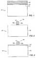
- FIG. 1a semiconductor substrate 101 that includes an n-doped epitaxially grown silicon layer 102 .
- a thermally grown pad oxide layer 104on which is formed a thick oxide layer 105 , which can comprise field oxide (FOX).
- FOXfield oxide
- the field oxidecan be removed from the device active area, and a thick oxide layer 105 comprising low temperature oxide (LTO) or undoped silicon glass (USG) can be formed thereon.
- Oxide layer 105has a thickness preferably of about 0.4 ⁇ m to about 1.5 ⁇ m, more preferably, about 0.8 ⁇ m.
- thick oxide layer 105is patterned by masking and anisotropic etching, for example, reactive ion etching, to form a narrow terraced gate oxide region 106 having a top surface 107 and two side surfaces 108 a and 108 b .
- a gate oxide layer 109is formed on epitaxial layer upper surface 103 , as depicted in FIG. 3 .
- FIG. 4illustrates the deposition of polysilicon layer 110 on terraced gate oxide region 106 and gate oxide layer 109
- FIG. 5depicts the anisotropic etching of layer 110 to form polysilicon spacers 111 a and 111 b abutting side surfaces 108 a and 108 b , respectively, of terraced gate oxide region 106
- a p-type dopant, boronfor example, is implanted at a dose of about 1 ⁇ 10 13 to 2 ⁇ 10 14 atoms/cm 2 at about 10 to 120 KeV through gate oxide layer 109 and a tapered portion of polysilicon spacers 111 a and 111 b into epitaxial layer 102 .
- spacers 111 a-benable automatic channel doping modulation. Driving of the boron dopant results in formation of P-well regions 112 a and 112 b , as shown in FIG. 6 . It should be noted that the process of the present invention results in complete self-alignment of terraced gate oxide region 106 , polysilicon spacers 111 a and 111 b , and P-well regions 112 a and 112 b.
- an n-type dopantsuch as phosphorus, arsenic, or mixtures thereof is implanted at a dose of about 1 ⁇ 10 15 to 2 ⁇ 10 16 atoms/cm 2 at about 10 to 120 KeV through gate oxide layer 109 and a tapered portion of polysilicon spacers 111 a and 111 b into P-well regions 112 a and 112 b .
- Annealingresults in the formation of N + source regions 113 a and 113 b in P-well regions 112 a and 112 b , respectively, as depicted in FIG. 8 .
- FIG. 9illustrates the Following removal of source mask M, a passivation layer 115 such as borophosphosilicate glass (BPSG) is formed on polysilicon spacers 111 a-b , on top surface 107 of narrow terraced gate region 106 , and on gate oxide layer 109 .
- BPSGborophosphosilicate glass
- the tapered form of polysilicon spacers 111 a-beliminates the need for the reflow treatment of BPSG that is typically required if the gate polysilicon is in the form of a planar layer with sharp edges.
- Portions of gate oxide layer 109 and passivation layer 115 overlying P-well regions 112 a-b and N + source regions 113 a-bare then removed to form P-well and N + source contact regions 114 a and 114 b.
- FIGS. 10-12illustrate alternative steps, starting with the structure depicted in FIG. 8, of the process of the present invention.
- FIG. 10is depicted the removal of polysilicon spacers 111 a and 111 b from their positions abutting narrow terraced gate region 106 .
- layer 109may be removed and regrown.
- FIG. 11depicts the optional formation of a barrier layer 116 , for example, titanium or titanium nitride, on terraced gate region 107 and gate oxide layer 109 .
- a layer 117 of gate metalfor example, aluminum, molybdenum, or tungsten, is formed on optional barrier layer 116 or on terraced gate oxide region 107 and gate oxide layer 109 .
- gate metal layer 117is anisotropically etched to form metal spacers 118 a and 118 b abutting side surfaces 108 a and 108 b , respectively, of narrow terraced gate region 107 .
- FIG. 13is a computer-simulated cross-section of a power semiconductor device 100 formed by the process of the present invention.
- Device 100includes a substrate 101 having an n-doped epitaxial layer 102 , a narrow terraced gate oxide region 106 , gate oxide layer 109 , tapered polysilicon spacers 111 a-b , P-well regions 112 , N + source regions 113 , well and source contact regions 114 , and passivation layer 115 .
- polysilicon spacers 111 a-bcan be replaced by tapered metal spacers 118 a-b .
- Metal layer 119is formed to provide contact with P-well and N + source contact regions 114 and with a gate contact region (not shown). Formation of a backside metal layer (not shown) completes the fabrication, in accordance with the present invention, of device 100 .
- FIG. 14is a computer-simulated cross-section of a prior art power semiconductor device 200 analogous to device 100 formed in accordance with the present invention.
- Device 200includes a substrate 201 having an n-doped epitaxial layer 202 , gate oxide layer 209 , gate polysilicon 211 , P-well regions 212 , N + source regions 213 , well and source contact regions 214 , and passivation layer 215 .
- Metal layer 219is formed to provide contact with P-well and N + source contact regions 214 and with a gate contact region (not shown). Formation of a backside metal layer (not shown) completes the fabrication of prior art device 200 .
- FIG. 15contains plots of gate charge as a function of gate voltage for device 100 of the invention and for prior art device 200 . Comparison of the plots makes clear that the “Miller” charge, which is defined as the width of the plateau in the curve, is dramatically reduced for device 100 relative to device 200 . Consequently, the switching speed of device 100 is very much faster than that of device 200 , as is clearly evident from the plots, included in FIG. 16, of gate voltage as a function of time for the two devices.
- the simulated data obtained for device 100 of the present invention and prior art device 200are summarized in TABLE 1.
- Device 100also has lower total input capacitance than device 200 , as demonstrated by the large difference in slope of the curves in FIGS. 15 and 16.
- the drain-source breakdown voltage, V dsbrof device 100 is slightly lower than that of device 200 because of the presence of the thick terraced gate oxide interrupting the gate polysilicon in device 100 .
- ESRgate equivalent series resistance
Landscapes
- Engineering & Computer Science (AREA)
- Physics & Mathematics (AREA)
- Condensed Matter Physics & Semiconductors (AREA)
- General Physics & Mathematics (AREA)
- Manufacturing & Machinery (AREA)
- Computer Hardware Design (AREA)
- Microelectronics & Electronic Packaging (AREA)
- Power Engineering (AREA)
- Electrodes Of Semiconductors (AREA)
- Insulated Gate Type Field-Effect Transistor (AREA)
Abstract
Description
The present invention relates to power semiconductor devices, more particularly, to MOSFET devices suitable for high frequency power conversion or RF applications, and to a process for making such devices.
The semiconductor industry is witnessing an increasing demand for DC-DC converters with low output voltage, very fast transient response, and high efficiency that can be advantageously used for high frequency power conversion. When the operating frequency reaches 1 MHz or higher, the power losses of a synchronous buck DC-DC converter will be dominated by the switching losses of output power MOSFETs. It is well known that most switching losses in a power MOSFET occur during charging/discharging the drain-gate capacitance, the so-called “Miller effect.” Reducing drain-source feedback capacitance, referred to as “Miller capacitance,” is an important approach to improving DC-DC converter efficiency. In addition, decreasing or completely eliminating Miller capacitance would dramatically improve the RF performance of the device. Conceptually, Miller capacitance can be substantially decreased by removing the polysilicon layer overlying the neck region, or by increasing the thickness of the oxide layer underneath the polysilicon layer in the neck region. These concepts are discussed in, for example, the following publications: K. Shenai, “Optimally scaled low-voltage vertical power MOSFETs for high-frequency power conversion” inIEEE Trans. Electron Dev., 1990, Vol. 37, No. 4, pp 1141-1153; O. Ishikawa and H. Esaki, “A high-power high-gain VD-MOSFET operating at 900 MHz” inIEEE Trans. Electron Dev., 1987, Vol. 34, No. 5, pp 1157-1161; and D. Ueda, H. Takagi, and G. Kano, “A new vertical double diffused MOSFET—The Self-Aligned Terraced-Gate MOSFET” inIEEE Trans. Electron Dev., 1984, Vol. 31, No. 4, pp 416-420. The disclosures of these papers are incorporated herein by reference.
Realizing the concepts discussed in the cited papers is a formidable fabrication challenge, requiring a multiplicity of masks, non-self aligned photolithographic steps, and non-standard processing steps. It would be highly desirable to devise a cost-effective, readily manufacturable self-aligned process for the fabrication of power MOSFETs with low Miller capacitance. This goal is met by the process of the present invention.
A process for forming a power semiconductor device with reduced input capacitance and improved switching speed comprises: providing a semiconductor substrate that includes an n-doped layer of epitaxially grown silicon, and forming a thick oxide layer on an upper surface of the epitaxial layer. Prior to formation of the thick oxide layer, a thin pad oxide layer is optionally grown on the epitaxial layer. The thick oxide layer is patterned to form a narrow terraced gate oxide region having a top surface and two side surfaces on the epitaxial layer upper surface. A gate oxide layer is formed on the upper surface of the epitaxial layer, and a layer of polysilicon is deposited on the narrow terraced gate oxide region and the gate oxide layer. The polysilicon layer is anisotropically etched to form tapered polysilicon spacers abutting each of the two side surfaces of the narrow terraced gate region.
A p-type dopant is implanted through the gate oxide layer and a tapered portion of the polysilicon spacers, and the dopant is driven to form P-well regions in the epitaxial layer at its upper surface. A source mask is formed on the epitaxial layer upper surface, and an n-type dopant is implanted through the gate oxide layer and a tapered portion of the polysilicon spacers, then driven to form N+ source regions in the P-well regions.
The process of the present invention further comprises: removing the source mask and forming a passivation layer on the polysilicon spacers, the top surface of the narrow terraced gate region, and the gate oxide layer overlying the epitaxial layer upper surface. Following removal of portions of the passivation layer and the gate oxide layer overlying the P-well and N+ source regions to form P-well and N+ source contact regions, a metal layer is formed that is in contact with the P-well and N+ source contact regions and with a gate contact region.
In another embodiment, the process of the present invention further comprises: removing the source mask and the polysilicon spacers from the epitaxial layer upper surface, and depositing a layer of gate metal on the narrow terraced gate oxide region and the gate oxide layer. The gate metal layer is anisotropically etched to form tapered metal spacers abutting each of the two side surfaces of the narrow terraced gate region, and a passivation layer is formed on the metal spacers, the top surface of the narrow terraced gate region, and the gate oxide layer overlying the epitaxial layer upper surface. Portions of the passivation layer and gate oxide layer overlying the P-well and N+ source regions are removed to form P-well and N+ source contact regions, and a metal layer is formed that is in contact with the P-well and N+ source contact regions and with a gate contact region.
FIGS. 1-9 schematically depict the steps employed in the process of the present invention.
FIGS. 10-12 depict further steps in the process of the invention.
FIGS. 13 and 14 are computer-simulated cross-sectional views of, respectively, a power semiconductor device formed by the process of the present invention and a prior art device.
FIGS. 15 and 16 are plots of, respectively, gate charge vs gate voltage and gate voltage vs time for computer simulations of the electrical performance of a device formed by the process of the present invention and a prior art device.
The process of the present invention is illustrated by FIGS. 1-9. In FIG. 1 is shown asemiconductor substrate 101 that includes an n-doped epitaxially grownsilicon layer 102. Onupper surface 103 ofepitaxial layer 102 is a thermally grown pad oxide layer104, on which is formed athick oxide layer 105, which can comprise field oxide (FOX). Alternatively, the field oxide can be removed from the device active area, and athick oxide layer 105 comprising low temperature oxide (LTO) or undoped silicon glass (USG) can be formed thereon.Oxide layer 105 has a thickness preferably of about 0.4 μm to about 1.5 μm, more preferably, about 0.8 μm.
As shown in FIG. 2,thick oxide layer 105 is patterned by masking and anisotropic etching, for example, reactive ion etching, to form a narrow terracedgate oxide region 106 having atop surface 107 and twoside surfaces gate oxide region 106, agate oxide layer 109 is formed on epitaxial layerupper surface 103, as depicted in FIG.3.
FIG. 4 illustrates the deposition ofpolysilicon layer 110 on terracedgate oxide region 106 andgate oxide layer 109, and FIG. 5 depicts the anisotropic etching oflayer 110 to formpolysilicon spacers side surfaces gate oxide region 106. A p-type dopant, boron, for example, is implanted at a dose of about 1×10¹³to 2×10¹⁴atoms/cm2at about 10 to 120 KeV throughgate oxide layer 109 and a tapered portion ofpolysilicon spacers epitaxial layer 102. The sloping sides of spacers111a-benables automatic channel doping modulation. Driving of the boron dopant results in formation of P-well regions gate oxide region 106,polysilicon spacers well regions
Following formation of a photoresist source mask M, as shown in FIG. 7, an n-type dopant such as phosphorus, arsenic, or mixtures thereof is implanted at a dose of about 1×10¹⁵to 2×10¹⁶atoms/cm2at about 10 to 120 KeV throughgate oxide layer 109 and a tapered portion ofpolysilicon spacers well regions well regions
FIG. 9 illustrates the Following removal of source mask M, apassivation layer 115 such as borophosphosilicate glass (BPSG) is formed on polysilicon spacers111a-b, ontop surface 107 of narrowterraced gate region 106, and ongate oxide layer 109. The tapered form of polysilicon spacers111a-beliminates the need for the reflow treatment of BPSG that is typically required if the gate polysilicon is in the form of a planar layer with sharp edges. Portions ofgate oxide layer 109 andpassivation layer 115 overlying P-well regions 112a-band N+ source regions113a-bare then removed to form P-well and N+source contact regions
FIGS. 10-12 illustrate alternative steps, starting with the structure depicted in FIG. 8, of the process of the present invention. In FIG. 10 is depicted the removal ofpolysilicon spacers terraced gate region 106. Optionally, to repair possible damage togate oxide layer 109 during removal ofspacers layer 109 may be removed and regrown. FIG. 11 depicts the optional formation of abarrier layer 116, for example, titanium or titanium nitride, onterraced gate region 107 andgate oxide layer 109. Alayer 117 of gate metal, for example, aluminum, molybdenum, or tungsten, is formed onoptional barrier layer 116 or on terracedgate oxide region 107 andgate oxide layer 109. As shown in FIG. 12,gate metal layer 117 is anisotropically etched to formmetal spacers side surfaces terraced gate region 107.
It will be noted that the structure depicted in FIG. 12, except for the use of metal rather than polysilicon in gate spacers118a-band the inclusion ofoptional barrier layer 116, is the same as that shown in FIG.8. The use of metal rather than polysilicon provides additional further advantages to devices formed by the process of the present invention: a very large reduction in gate signal propagation equivalent series resistance (ESR), and a greatly enhanced transient response during on/off switching of the device. The metal spacers also substantially improve the RF performance of the device.
FIG. 13 is a computer-simulated cross-section of apower semiconductor device 100 formed by the process of the present invention.Device 100 includes asubstrate 101 having an n-dopedepitaxial layer 102, a narrow terracedgate oxide region 106,gate oxide layer 109, tapered polysilicon spacers111a-b, P-well regions 112, N+ source regions113, well andsource contact regions 114, andpassivation layer 115. As already noted, polysilicon spacers111a-bcan be replaced by tapered metal spacers118a-b.Metal layer 119 is formed to provide contact with P-well and N+source contact regions 114 and with a gate contact region (not shown). Formation of a backside metal layer (not shown) completes the fabrication, in accordance with the present invention, ofdevice 100.
FIG. 14 is a computer-simulated cross-section of a prior artpower semiconductor device 200 analogous todevice 100 formed in accordance with the present invention.Device 200 includes asubstrate 201 having an n-dopedepitaxial layer 202,gate oxide layer 209,gate polysilicon 211, P-well regions 212, N+ source regions213, well andsource contact regions 214, andpassivation layer 215.Metal layer 219 is formed to provide contact with P-well and N+source contact regions 214 and with a gate contact region (not shown). Formation of a backside metal layer (not shown) completes the fabrication ofprior art device 200.
Computer simulation was employed to compare the electrical performance ofdevices device 100 of the invention and forprior art device 200. Comparison of the plots makes clear that the “Miller” charge, which is defined as the width of the plateau in the curve, is dramatically reduced fordevice 100 relative todevice 200. Consequently, the switching speed ofdevice 100 is very much faster than that ofdevice 200, as is clearly evident from the plots, included in FIG. 16, of gate voltage as a function of time for the two devices.
The simulated data obtained fordevice 100 of the present invention andprior art device 200 are summarized in TABLE 1. Although the threshold voltage, Vth, and specific on-resistance, Rsp, are almost identical for both devices, the “Miller” charge, Qgd, ofdevice 100 is 56% lower than that ofdevice 200.Device 100 also has lower total input capacitance thandevice 200, as demonstrated by the large difference in slope of the curves in FIGS. 15 and 16. The drain-source breakdown voltage, Vdsbr, ofdevice 100 is slightly lower than that ofdevice 200 because of the presence of the thick terraced gate oxide interrupting the gate polysilicon indevice 100. The reduction of polysilicon area in the latter device may increase the gate equivalent series resistance (ESR), which can be compensated by increasing the polysilicon dopant concentration. Also, as previously noted, substitution of metal for polysilicon in the gate spacers results in a very large reduction in ESR.
| TABLE 1 | ||||
| Device | Vth(V) | Rsp@ 10 V (mohm.cm2) | Vdsbr(V) | Ogd(nC/ |
| 100 | 1.76 | 0.55 | 32 | 41 |
| 200 | 1.77 | 0.58 | 35 | 93 |
The invention has been described in detail for the purpose of illustration, but it is to be understood that such detail is solely for that purpose, and variations can be made therein by those skilled in the art without departing from the spirit and scope of the invention, which is defined by the claims that follow.
Claims (39)
1. A process for forming a power semiconductor device with reduced input capacitance and improved switching speed, said process comprising:
providing a semiconductor substrate comprising a layer of n-doped epitaxially grown silicon;
forming a thick oxide layer on an upper surface of said epitaxial layer;
patterning said thick oxide layer, thereby forming a narrow terraced gate oxide region on said upper surface of said epitaxial layer, said narrow terraced gate oxide region having a top surface and two side surfaces;
forming a gate oxide layer on said upper surface of said epitaxial layer;
depositing a layer of polysilicon on said narrow terraced gate oxide region and said gate oxide layer;
anisotropically etching said polysilicon layer, thereby forming tapered polysilicon spacers abutting each of said two side surfaces of said narrow terraced gate oxide region;
implanting a p-type dopant through said gate oxide layer and a tapered portion of said polysilicon spacers, and driving said p-type dopant in said epitaxial layer, thereby forming p-well regions in said epitaxial layer at its upper surface; and
forming a source mask on said epitaxial layer upper surface, implanting an n-type dopant through said gate oxide layer and a tapered portion of said polysilicon spacers, and driving said n-type dopant in said P-well regions, thereby forming N+ source regions in said P-well regions.
2. The process ofclaim 1 further comprising:
removing said source mask, and forming a passivation layer on said polysilicon spacers, on said top surface of said narrow terraced gate oxide region, and on said gate oxide layer overlying said epitaxial layer upper surface;
removing portions of said passivation layer and said gate oxide layer overlying said P-well and N+ source regions, thereby forming P-well and N+ source contact regions; and
forming a metal layer in contact with said P-well and N+ source contact regions and with a gate contact region.
3. The process ofclaim 2 wherein said passivating layer is borophosphosilicate glass (BPSG).
4. A power semiconductor device formed by the process ofclaim 2 .
5. The process ofclaim 1 further comprising:
removing said source mask and said polysilicon spacers from said epitaxial layer upper surface;
depositing a layer of gate metal on said narrow terraced gate oxide region and said gate oxide layer;
anisotropically etching said gate metal layer, thereby forming tapered metal spacers abutting each of two side surfaces of said narrow terraced gate region;
forming a passivation layer on said metal spacers, on said top surface of said narrow terraced gate region, and on said gate oxide layer overlying said epitaxial layer upper surface;
removing portions of said passivation layer and said gate oxide layer overlying said P-well and N+ source regions, thereby forming P-well and N source contact regions; and
forming a metal layer in contact with said P-well and N30 source contact regions and with a gate contact region.
6. The process ofclaim 5 wherein said gate metal is selected from the group consisting of aluminum, molybdenum, and tungsten.
7. The process ofclaim 5 further comprising:
prior to depositing said layer of gate metal, forming a barrier layer on said narrow terraced gate oxide region and said gate oxide layer.
8. The process ofclaim 7 wherein said barrier layer comprises titanium or titanium nitride.
9. A power semiconductor device formed by the process ofclaim 5 .
10. The process ofclaim 1 further comprising:
prior to forming said thick oxide layer, growing a thin pad oxide layer on an upper surface of said epitaxial layer.
11. The process ofclaim 5 further comprising:
in addition to removing said source mask and said polysilicon spacers, removing said gate oxide layer from said epitaxial layer upper surface; and
forming a new gate oxide layer on said epitaxial layer upper surface.
12. The process ofclaim 1 wherein said thick oxide layer comprises an oxide selected from the group consisting of field oxide (FOX), low temperature oxide (LTO) and undoped silicon glass (USG).
13. The process ofclaim 1 wherein said thick oxide layer has a thickness of about 0.4 μm to about 1.5 μm.
14. The process ofclaim 13 wherein said thick oxide layer has a thickness of about 0.8 μm.
15. The process ofclaim 1 wherein said p-type dopant is boron.
16. The process ofclaim 1 wherein said p-type dopant is at a dose of about 1×10¹⁴atoms/cm2at about 10 to 120 KeV.
17. The process ofclaim 1 wherein said n-type dopant is phosphorus, arsenic or a mixture thereof.
18. The process ofclaim 1 wherein said n-type dopant is a dose of about 1×10¹⁵to 2×10¹⁶atoms/cm2at about 10 to 120 KeV.
19. A power semiconductor device formed by the process ofclaim 1 .
20. The process ofclaim 1 further comprising:
removing said source mask, and forming a passivation layer on said polysilicon spacers, on said top surface of said marrow terraced gate region, and on said gate oxide layer overlying said epitaxial layer upper surface;
removing portions of said passivation layer and gate oxide layer overlying said well and source contact regions; and
forming a metal layer in contact with said well and source contact regions and with a gate contact region.
21. The process ofclaim 20 wherein said passivating layer is borophosphosilicate glass (BPSG).
22. A power semiconductor device formed by the process ofclaim 20 .
23. A process for forming a power semiconductor device with reduced input capacitance and improved switching speed, said process comprising:
providing a semiconductor substrate comprising a layer of n-doped epitaxially grown silicon;
forming a thick oxide layer on an upper surface of said epitaxial layer;
patterning said thick oxide layer, thereby forming a narrow terraced gate oxide region on said upper surface of said epitaxial layer, said narrow terraced gate oxide region having a top surface and two side surfaces;
forming a gate oxide layer on said upper surface of said epitaxial layer;
depositing a layer of polysilicon on said narrow terraced gate oxide region and said gate oxide layer;
anisotropically etching said polysilicon layer, thereby forming tapered polysilicon spacers abutting each of said two side surfaces of said narrow terraced gate oxide region;
implanting a dopant of a first polarity through said gate oxide layer and a tapered portion of said polysilicon spacers, and driving said first polarity dopant in said epitaxial layer, thereby forming well regions in said epitaxial layer at its upper surface; and
forming a source mask on said epitaxial layer upper surface, implanting a dopant of a second polarity through said gate oxide layer and a tapered portion of said polysilicon spacers, and driving said dopant of the second polarity in said well regions, thereby forming heavily doped source regions in said well regions.
24. The process ofclaim 23 further comprising:
removing said source mask and said polysilicon spacers from said epitaxial layer upper surface;
depositing a layer of gate metal on said narrow terraced gate oxide region and said gate oxide layer;
anisotopically etching said gate metal layer, thereby forming tapered metal spacers abutting each of two side surfaces of said narrow terraced gate oxide region;
forming a passivation layer on said metal spacers, on said top surface of said narrow terraced gate oxide region, and on said gate oxide layer overlying said epitaxial layer upper surface;
removing portions of said passivation layer and said gate oxide layer overlying said well and source regions, thereby forming well and source contact regions; and
forming a metal layer in contact with said well and source contact regions and with a gate contact region.
25. The process ofclaim 24 wherein said gate metal is selected from the group consisting of aluminum, molybdenum and tungsten.
26. The process ofclaim 24 further comprising:
in addition to removing said source mask and said polysilicon spacers, removing said gate oxide layer from said epitaxial layer upper surface; and
forming a new gate oxide layer on said epitaxial layer upper surface.
27. The process ofclaim 24 further comprising:
prior to depositing said layer of gate metal, forming a barrier layer on said narrow terraced gate oxide region and said gate oxide layer.
28. The process ofclaim 27 wherein said barrier layer comprises titanium or titanium nitride.
29. A power semiconductor device formed by the process ofclaim 24 .
30. The process ofclaim 23 further comprising:
prior to forming said thick oxide layer, growing a thin pad oxide layer on an upper surface of said epitaxial layer.
31. The process ofclaim 23 wherein said thick oxide layer comprises an oxide selected from the group consisting of field oxide (FOX), low temperature oxide (LTO) and undoped silicon glass (USG).
32. The process ofclaim 23 wherein said thick oxide layer has a thickness of about 0.4 μm to about 1.5 μm.
33. The process ofclaim 32 wherein said thick oxide layer has a thickness of about 0.8 μm.
34. The process ofclaim 23 wherein said first polarity type dopant is boron.
35. The process ofclaim 27 wherein said first polarity type dopant is at a dose of about 1×10¹⁴atoms/cm2at about 10 to 120 KeV.
36. The process ofclaim 23 wherein said second type polarity dopant is phosphorus, arsenic or a mixture thereof.
37. The process ofclaim 23 wherein said second polarity type dopant is a dose of about 1×10¹⁵to 2×10¹⁶atoms/cm2at about 10 to 120 KeV.
38. The process ofclaim 23 wherein the first polarity type dopant is n-type and the second polarity type dopant is p-type.
39. A power semiconductor devise formed by the process ofclaim 23 .
Priority Applications (1)
| Application Number | Priority Date | Filing Date | Title |
|---|---|---|---|
| US09/665,850US6589830B1 (en) | 2000-09-20 | 2000-09-20 | Self-aligned process for fabricating power MOSFET with spacer-shaped terraced gate |
Applications Claiming Priority (1)
| Application Number | Priority Date | Filing Date | Title |
|---|---|---|---|
| US09/665,850US6589830B1 (en) | 2000-09-20 | 2000-09-20 | Self-aligned process for fabricating power MOSFET with spacer-shaped terraced gate |
Publications (1)
| Publication Number | Publication Date |
|---|---|
| US6589830B1true US6589830B1 (en) | 2003-07-08 |
Family
ID=24671806
Family Applications (1)
| Application Number | Title | Priority Date | Filing Date |
|---|---|---|---|
| US09/665,850Expired - Fee RelatedUS6589830B1 (en) | 2000-09-20 | 2000-09-20 | Self-aligned process for fabricating power MOSFET with spacer-shaped terraced gate |
Country Status (1)
| Country | Link |
|---|---|
| US (1) | US6589830B1 (en) |
Cited By (8)
| Publication number | Priority date | Publication date | Assignee | Title |
|---|---|---|---|---|
| US20040121524A1 (en)* | 2002-12-20 | 2004-06-24 | Micron Technology, Inc. | Apparatus and method for controlling diffusion |
| US6756644B2 (en) | 2001-03-28 | 2004-06-29 | International Rectifier Corporation | Ultra low QGD power MOSFET |
| WO2004066395A3 (en)* | 2003-01-21 | 2004-09-02 | Univ Northwest | Fast switching power insulated gate semiconductor device |
| US20050116298A1 (en)* | 2003-11-07 | 2005-06-02 | Jenoe Tihanyi | MOS field effect transistor with small miller capacitance |
| US20060249785A1 (en)* | 2005-05-09 | 2006-11-09 | Alpha And Omega Semiconductor, Ltd | Power MOSFET device structure for high frequency applications |
| US20080070392A1 (en)* | 2003-04-22 | 2008-03-20 | Micron Technology, Inc. | Controlling diffusion in doped semiconductor regions |
| US20090159896A1 (en)* | 2007-12-20 | 2009-06-25 | General Electric Company | Silicon carbide mosfet devices and methods of making |
| US20120025299A1 (en)* | 2010-07-30 | 2012-02-02 | Ko Soo-Byung | Method for fabricating semiconductor device with buried gates |
Citations (3)
| Publication number | Priority date | Publication date | Assignee | Title |
|---|---|---|---|---|
| US5510281A (en)* | 1995-03-20 | 1996-04-23 | General Electric Company | Method of fabricating a self-aligned DMOS transistor device using SiC and spacers |
| US6186408B1 (en)* | 1999-05-28 | 2001-02-13 | Advanced Power Devices, Inc. | High cell density power rectifier |
| US6331455B1 (en)* | 1999-04-01 | 2001-12-18 | Advanced Power Devices, Inc. | Power rectifier device and method of fabricating power rectifier devices |
- 2000
- 2000-09-20USUS09/665,850patent/US6589830B1/ennot_activeExpired - Fee Related
Patent Citations (4)
| Publication number | Priority date | Publication date | Assignee | Title |
|---|---|---|---|---|
| US5510281A (en)* | 1995-03-20 | 1996-04-23 | General Electric Company | Method of fabricating a self-aligned DMOS transistor device using SiC and spacers |
| US5814859A (en)* | 1995-03-20 | 1998-09-29 | General Electric Company | Self-aligned transistor device including a patterned refracting dielectric layer |
| US6331455B1 (en)* | 1999-04-01 | 2001-12-18 | Advanced Power Devices, Inc. | Power rectifier device and method of fabricating power rectifier devices |
| US6186408B1 (en)* | 1999-05-28 | 2001-02-13 | Advanced Power Devices, Inc. | High cell density power rectifier |
Non-Patent Citations (3)
| Title |
|---|
| Ishikawa, Osamu, et al., "A High-Power High-Gain VD-MOSFET Operating at 900 MHz", IEEE Transactions On Electron Devices, vol. ED. 34, No. 5., May 1987 (pp. 1157-1161). |
| Shenai, Krishna, "Optimally Scaled Low-Voltage Vertical Power MOSFET's for High-Frequency Power Conversion", IEEE Transactions On Electron Devices, vol. 37, No. 4, Apr. 1990 (pp. 1141)-1153). |
| Ueda, Daisuke et al., "A New Vertical Double Diffused MOSFET-The Self-Aligned Terraced-Gate MOSFET", IEEE Transactions On Electron Devices, vol. ED 31, No. 4, Apr. 1984 (pp. 416-420). |
Cited By (19)
| Publication number | Priority date | Publication date | Assignee | Title |
|---|---|---|---|---|
| US6756644B2 (en) | 2001-03-28 | 2004-06-29 | International Rectifier Corporation | Ultra low QGD power MOSFET |
| US7592242B2 (en)* | 2002-12-20 | 2009-09-22 | Micron Technology, Inc. | Apparatus and method for controlling diffusion |
| US20040121524A1 (en)* | 2002-12-20 | 2004-06-24 | Micron Technology, Inc. | Apparatus and method for controlling diffusion |
| US9147735B2 (en) | 2002-12-20 | 2015-09-29 | Micron Technology, Inc. | Apparatus and method for controlling diffusion |
| US20060003559A1 (en)* | 2002-12-20 | 2006-01-05 | Micron Technology, Inc. | apparatus and method for controlling diffusion |
| US20060003535A1 (en)* | 2002-12-20 | 2006-01-05 | Micron Technology, Inc. | Apparatus and method for controlling diffusion |
| US20100237422A1 (en)* | 2002-12-20 | 2010-09-23 | Farrar Paul A | Apparatus and method for controlling diffusion |
| US7727868B2 (en) | 2002-12-20 | 2010-06-01 | Micron Technology, Inc. | Apparatus and method for controlling diffusion |
| US20060118832A1 (en)* | 2003-01-21 | 2006-06-08 | North-West University | Fast switching power insulated gate semiconductor device |
| WO2004066395A3 (en)* | 2003-01-21 | 2004-09-02 | Univ Northwest | Fast switching power insulated gate semiconductor device |
| US20080203457A1 (en)* | 2003-01-21 | 2008-08-28 | North-West University | Fast switching power insulated gate semiconductor device |
| US8063426B2 (en) | 2003-01-21 | 2011-11-22 | North-West University | Fast switching power insulated gate semiconductor device |
| US7585753B2 (en) | 2003-04-22 | 2009-09-08 | Micron Technology, Inc. | Controlling diffusion in doped semiconductor regions |
| US20080070392A1 (en)* | 2003-04-22 | 2008-03-20 | Micron Technology, Inc. | Controlling diffusion in doped semiconductor regions |
| US20050116298A1 (en)* | 2003-11-07 | 2005-06-02 | Jenoe Tihanyi | MOS field effect transistor with small miller capacitance |
| US7659570B2 (en) | 2005-05-09 | 2010-02-09 | Alpha & Omega Semiconductor Ltd. | Power MOSFET device structure for high frequency applications |
| US20060249785A1 (en)* | 2005-05-09 | 2006-11-09 | Alpha And Omega Semiconductor, Ltd | Power MOSFET device structure for high frequency applications |
| US20090159896A1 (en)* | 2007-12-20 | 2009-06-25 | General Electric Company | Silicon carbide mosfet devices and methods of making |
| US20120025299A1 (en)* | 2010-07-30 | 2012-02-02 | Ko Soo-Byung | Method for fabricating semiconductor device with buried gates |
Similar Documents
| Publication | Publication Date | Title |
|---|---|---|
| JP4198469B2 (en) | Power device and manufacturing method thereof | |
| US11652166B2 (en) | Power device having super junction and Schottky diode | |
| US6586833B2 (en) | Packaged power devices having vertical power mosfets therein that are flip-chip mounted to slotted gate electrode strip lines | |
| KR100869324B1 (en) | Power semiconductor device with side extension base shielding area to prevent base rich-through and manufacturing method thereof | |
| US7538370B2 (en) | Semiconductor device having reduced gate charge and reduced on resistance and method | |
| US20020185679A1 (en) | Power semiconductor devices having linear transfer characteristics and methods of forming and operating same | |
| CN110459539B (en) | Shielded gate trench MOSFET with integrated ESD protection and manufacturing method | |
| US20070215914A1 (en) | Power semiconductor device having improved performance and method | |
| US6589830B1 (en) | Self-aligned process for fabricating power MOSFET with spacer-shaped terraced gate | |
| JP2003101019A (en) | Semiconductor device and manufacturing method thereof | |
| DE102013107123A1 (en) | Charge compensation semiconductor device | |
| CN106057902A (en) | High performance MOSFET and manufacturing method thereof | |
| CN116190419B (en) | Super-junction power MOSFET structure for optimizing linear output and preparation method thereof | |
| CN117174758B (en) | SGT MOSFET device and preparation method | |
| CN118099221B (en) | Silicon carbide power device and manufacturing method thereof | |
| CN120111934B (en) | Semiconductor structure and preparation method thereof | |
| CN106252415B (en) | A kind of high performance MOSFET and its manufacturing method | |
| CN120091608A (en) | A MOSFET device with electric field and carrier modulation | |
| CN117153885A (en) | Split gate trench MOSFET device and preparation method | |
| CN115663026A (en) | High voltage depletion mode field effect transistor and method of forming the same |
Legal Events
| Date | Code | Title | Description |
|---|---|---|---|
| AS | Assignment | Owner name:INTERSIL CORPORATION, FLORIDA Free format text:ASSIGNMENT OF ASSIGNORS INTEREST;ASSIGNOR:ZENG, JUN;REEL/FRAME:011106/0468 Effective date:20000914 | |
| AS | Assignment | Owner name:INTERSIL HOLDING CORPORATION, CALIFORNIA Free format text:INTELLECTUAL PROPERTY PARTIAL RELEASE;ASSIGNOR:CREIDT SUISSE FIRST BOSTON;REEL/FRAME:011667/0166 Effective date:20010303 | |
| AS | Assignment | Owner name:FAIRCHILD SEMICONDUCTOR CORPORATION, MAINE Free format text:REASSIGNMENT OF PATENT APPLICATIONS;ASSIGNOR:INTERSIL CORPORATION;REEL/FRAME:012002/0206 Effective date:20010406 | |
| CC | Certificate of correction | ||
| FPAY | Fee payment | Year of fee payment:4 | |
| FPAY | Fee payment | Year of fee payment:8 | |
| REMI | Maintenance fee reminder mailed | ||
| LAPS | Lapse for failure to pay maintenance fees | ||
| STCH | Information on status: patent discontinuation | Free format text:PATENT EXPIRED DUE TO NONPAYMENT OF MAINTENANCE FEES UNDER 37 CFR 1.362 | |
| FP | Lapsed due to failure to pay maintenance fee | Effective date:20150708 |