US6589407B1 - Aluminum deposition shield - Google Patents
Aluminum deposition shieldDownload PDFInfo
- Publication number
- US6589407B1 US6589407B1US08/862,537US86253797AUS6589407B1US 6589407 B1US6589407 B1US 6589407B1US 86253797 AUS86253797 AUS 86253797AUS 6589407 B1US6589407 B1US 6589407B1
- Authority
- US
- United States
- Prior art keywords
- deposition shield
- thickness
- cylindrical portion
- inches
- chamber
- Prior art date
- Legal status (The legal status is an assumption and is not a legal conclusion. Google has not performed a legal analysis and makes no representation as to the accuracy of the status listed.)
- Expired - Lifetime, expires
Links
- 230000008021depositionEffects0.000titleclaimsabstractdescription36
- XAGFODPZIPBFFR-UHFFFAOYSA-NaluminiumChemical compound[Al]XAGFODPZIPBFFR-UHFFFAOYSA-N0.000titleclaimsabstractdescription23
- 229910052782aluminiumInorganic materials0.000titleclaimsabstractdescription23
- 229910001220stainless steelInorganic materials0.000claimsabstractdescription10
- 239000010935stainless steelSubstances0.000claimsabstractdescription10
- 238000001816coolingMethods0.000claimsabstractdescription8
- 239000000463materialSubstances0.000claimsdescription5
- 238000000034methodMethods0.000claims7
- 238000000151depositionMethods0.000description16
- 239000000758substrateSubstances0.000description10
- 235000012431wafersNutrition0.000description8
- 239000004065semiconductorSubstances0.000description4
- HJJVPARKXDDIQD-UHFFFAOYSA-NbromuconazoleChemical compoundClC1=CC(Cl)=CC=C1C1(CN2N=CN=C2)OCC(Br)C1HJJVPARKXDDIQD-UHFFFAOYSA-N0.000description2
- 239000004020conductorSubstances0.000description2
- 238000005240physical vapour depositionMethods0.000description2
- RYGMFSIKBFXOCR-UHFFFAOYSA-NCopperChemical compound[Cu]RYGMFSIKBFXOCR-UHFFFAOYSA-N0.000description1
- RTAQQCXQSZGOHL-UHFFFAOYSA-NTitaniumChemical compound[Ti]RTAQQCXQSZGOHL-UHFFFAOYSA-N0.000description1
- NRTOMJZYCJJWKI-UHFFFAOYSA-NTitanium nitrideChemical compound[Ti]#NNRTOMJZYCJJWKI-UHFFFAOYSA-N0.000description1
- 230000004888barrier functionEffects0.000description1
- 238000009529body temperature measurementMethods0.000description1
- WYEMLYFITZORAB-UHFFFAOYSA-NboscalidChemical compoundC1=CC(Cl)=CC=C1C1=CC=CC=C1NC(=O)C1=CC=CN=C1ClWYEMLYFITZORAB-UHFFFAOYSA-N0.000description1
- 239000002826coolantSubstances0.000description1
- 239000000498cooling waterSubstances0.000description1
- 239000010949copperSubstances0.000description1
- 229910052802copperInorganic materials0.000description1
- 230000005484gravityEffects0.000description1
- 239000012212insulatorSubstances0.000description1
- 230000005855radiationEffects0.000description1
- 229910052715tantalumInorganic materials0.000description1
- GUVRBAGPIYLISA-UHFFFAOYSA-Ntantalum atomChemical compound[Ta]GUVRBAGPIYLISA-UHFFFAOYSA-N0.000description1
- MZLGASXMSKOWSE-UHFFFAOYSA-Ntantalum nitrideChemical compound[Ta]#NMZLGASXMSKOWSE-UHFFFAOYSA-N0.000description1
- 239000010936titaniumSubstances0.000description1
- 229910052719titaniumInorganic materials0.000description1
- 238000001771vacuum depositionMethods0.000description1
Images

Classifications
- H—ELECTRICITY
- H01—ELECTRIC ELEMENTS
- H01J—ELECTRIC DISCHARGE TUBES OR DISCHARGE LAMPS
- H01J37/00—Discharge tubes with provision for introducing objects or material to be exposed to the discharge, e.g. for the purpose of examination or processing thereof
- H01J37/32—Gas-filled discharge tubes
- H01J37/32431—Constructional details of the reactor
- H01J37/32623—Mechanical discharge control means
- H01J37/32651—Shields, e.g. dark space shields, Faraday shields
- H—ELECTRICITY
- H01—ELECTRIC ELEMENTS
- H01J—ELECTRIC DISCHARGE TUBES OR DISCHARGE LAMPS
- H01J37/00—Discharge tubes with provision for introducing objects or material to be exposed to the discharge, e.g. for the purpose of examination or processing thereof
- H01J37/32—Gas-filled discharge tubes
- H01J37/32431—Constructional details of the reactor
- H01J37/32623—Mechanical discharge control means
- H—ELECTRICITY
- H01—ELECTRIC ELEMENTS
- H01J—ELECTRIC DISCHARGE TUBES OR DISCHARGE LAMPS
- H01J37/00—Discharge tubes with provision for introducing objects or material to be exposed to the discharge, e.g. for the purpose of examination or processing thereof
- H01J37/32—Gas-filled discharge tubes
- H01J37/34—Gas-filled discharge tubes operating with cathodic sputtering
- H01J37/3411—Constructional aspects of the reactor
- H01J37/3441—Dark space shields
Definitions
- the present inventionrelates to an apparatus for processing wafers in a vacuum chamber. More particularly, the invention relates to an apparatus for removal of heat from a vacuum chamber.
- a power sourcesuch as a radio frequency (“RF”) power source
- a devicesuch as an RF antenna coil
- Connecting a power source, such as a radio frequency (“RF”) power source, to a device, such as an RF antenna coil, through the wall of a vacuum chambertypically involves providing an insulated passage through one or more deposition shields.
- Application of RF energy to the coiltends to generate heat within the chamber. This heat is dissipated through radiation and conduction to heat sinks typically the shield, target, etc. within the chamber.
- Deposition shieldsare typically constructed of stainless steel for strength and tend to be negatively charged or grounded during wafer processing. Furthermore, the shield accumulates heat during wafer processing and chamber cooling declines unless the additional heat is removed from the shield. There is a need, therefore, for a deposition shield which avoids build up of additional heat within the vacuum chamber.
- the present inventionprovides an aluminum deposition shield which substantially improves transfer of radiated heat from within the vacuum chamber, to external chamber components in comparison to a conventional stainless steel deposition shield.
- the aluminum deposition shieldremains cooler during wafer processing and assists in cooling the chamber components.
- FIG. 1is a sectional view of a vacuum deposition chamber (without a target assembly) showing an external RF power source connected to a flat RF electrode coil within an aluminum deposition shield;
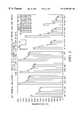
- FIG. 2compares the processing temperatures of deposition shields which are constructed from stainless steel or aluminum.
- the present inventionprovides an aluminum deposition shield within a vacuum chamber to enhance removal of radiated or conducted heat from an internal heat source such as an RF electrode.
- the vacuum chambercan be any plasma enhanced processing chamber wherein external RF or DC power is connected to a device within the vacuum chamber. Cooling of the vacuum chamber is enhanced since aluminum has a higher heat transfer co-efficient in comparison to stainless steel.
- the aluminum deposition shieldsare especially useful for cooling an electrode within a high density plasma vacuum semiconductor processing chamber such as the VECTRA® IMP chamber available from Applied Materials, Inc. of Santa Clara, Calif.
- the high vacuum chambersare used for physical vapor deposition (PVD) of Aluminum, Titanium, Copper, Tantalum, Tantalum Nitride, or Titanium Nitride layers to form conductors or barrier layers on semiconductor wafers.
- PVDphysical vapor deposition
- One or more VECTRA® IMP chambersare typically mounted on a semiconductor processing platform such as the ENDURA® platform manufactured by Applied Materials, Inc.
- the present inventionrelates to a useful apparatus for processing a substrate in a semiconductor processing chamber 10 .
- the processing chamber 10typically includes a clamp ring 12 and a support member 14 disposed in the processing chamber 10 , and a substrate alignment member 16 located on the support member 14 .
- the substrate alignment member 16aligns a substrate 18 with the support member 14 under gravity feed as the substrate is received on the support member 14 .
- a substrate lift mechanism 20moves pins 22 to receive the substrate prior to processing in the chamber.
- a support lift mechanism 24raises the support member 14 so that the support member 14 picks up the substrate 18 off the pins 22 prior to processing in the chamber, or lowers the support member 14 to place the substrate on the pins 22 for removal of the substrate after processing.
- An aluminum adapter 28supports the aluminum deposition shield 26 and an insulator 30 .
- the adapter 28is a wall of the vacuum chamber and typically has passages (not shown) for cooling water.
- An external RF power source 36supplies RF power to the antenna coil 32 which is externally grounded.
- the coil 32is supported within the chamber on a plurality of standoffs 34 .
- the coil 32is supplied with power to enable a gas, maintained at a vacuum pressure level in the chamber, to be energized into a plasma.
- the coil 32may optionally be supplied with a coolant through a central passage.
- conductive elementsmust extend through the chamber wall, but they cannot contact the chamber wall which may be grounded, or, if contacted with the conductor, will become “hot.”
- an insulated feed through(not shown) is typically extended though the adaptor.
- the aluminum deposition shieldmust be thicker than a comparable stainless steel shield to provide equivalent strength. However, a higher heat transfer co-efficient provides better cooling.
- the shield 26is configured to have a thin lip 25 which engages the conventional clamp ring 12 . The remainder of the shield 26 is thicker than comparable stainless steel shields unless a narrow region is needed for close tolerances.
- Performance of aluminum deposition shields Examples 2-6 of the present inventionwas simulated under wafer processing conditions and compared to a stainless steel shield Example C1. During wafer processing, the wafer was heated to 200° C. Each shield was supported by connectors which provides some convection of heat to the shield. Temperatures within the vacuum chamber were recorded at the wafer center, the shield bottom, the shield top, the shield middle, the coil bottom, the coil top, and the coil bottom. Thickness of the shields are shown in FIG. 2 along with the temperature measurements. The thicker aluminum shields 5 , 6 provided the lowest steady state shield temperatures.
Landscapes
- Engineering & Computer Science (AREA)
- Physics & Mathematics (AREA)
- Plasma & Fusion (AREA)
- Chemical & Material Sciences (AREA)
- Analytical Chemistry (AREA)
- Power Engineering (AREA)
- Physical Vapour Deposition (AREA)
- Chemical Vapour Deposition (AREA)
- Physical Deposition Of Substances That Are Components Of Semiconductor Devices (AREA)
- Plasma Technology (AREA)
Abstract
Description
The present invention relates to an apparatus for processing wafers in a vacuum chamber. More particularly, the invention relates to an apparatus for removal of heat from a vacuum chamber.
Connecting a power source, such as a radio frequency (“RF”) power source, to a device, such as an RF antenna coil, through the wall of a vacuum chamber typically involves providing an insulated passage through one or more deposition shields. Application of RF energy to the coil tends to generate heat within the chamber. This heat is dissipated through radiation and conduction to heat sinks typically the shield, target, etc. within the chamber. Deposition shields are typically constructed of stainless steel for strength and tend to be negatively charged or grounded during wafer processing. Furthermore, the shield accumulates heat during wafer processing and chamber cooling declines unless the additional heat is removed from the shield. There is a need, therefore, for a deposition shield which avoids build up of additional heat within the vacuum chamber.
The present invention provides an aluminum deposition shield which substantially improves transfer of radiated heat from within the vacuum chamber, to external chamber components in comparison to a conventional stainless steel deposition shield. The aluminum deposition shield remains cooler during wafer processing and assists in cooling the chamber components.
So that the manner in which the above recited features, advantages and objects of the present invention are attained and can be understood in detail, a more particular description of the invention, briefly summarized above, may be had by reference to the embodiments thereof which are illustrated in the appended drawings. The appended drawings illustrate typical embodiments of this invention and are not to be considered limiting of its scope, for the invention may admit to other equally effective embodiments.
FIG. 1 is a sectional view of a vacuum deposition chamber (without a target assembly) showing an external RF power source connected to a flat RF electrode coil within an aluminum deposition shield;
FIG. 2 compares the processing temperatures of deposition shields which are constructed from stainless steel or aluminum.
The present invention provides an aluminum deposition shield within a vacuum chamber to enhance removal of radiated or conducted heat from an internal heat source such as an RF electrode. The vacuum chamber can be any plasma enhanced processing chamber wherein external RF or DC power is connected to a device within the vacuum chamber. Cooling of the vacuum chamber is enhanced since aluminum has a higher heat transfer co-efficient in comparison to stainless steel.
The aluminum deposition shields are especially useful for cooling an electrode within a high density plasma vacuum semiconductor processing chamber such as the VECTRA® IMP chamber available from Applied Materials, Inc. of Santa Clara, Calif. The high vacuum chambers are used for physical vapor deposition (PVD) of Aluminum, Titanium, Copper, Tantalum, Tantalum Nitride, or Titanium Nitride layers to form conductors or barrier layers on semiconductor wafers. One or more VECTRA® IMP chambers are typically mounted on a semiconductor processing platform such as the ENDURA® platform manufactured by Applied Materials, Inc.
The invention is further described by reference to a specific aluminum deposition shield shown in the drawings, and by reference to comparisons to deposition shields made from other materials.
As shown in FIG. 1, the present invention relates to a useful apparatus for processing a substrate in asemiconductor processing chamber 10. Theprocessing chamber 10 typically includes aclamp ring 12 and asupport member 14 disposed in theprocessing chamber 10, and asubstrate alignment member 16 located on thesupport member 14. Thesubstrate alignment member 16 aligns asubstrate 18 with thesupport member 14 under gravity feed as the substrate is received on thesupport member 14. Asubstrate lift mechanism 20 movespins 22 to receive the substrate prior to processing in the chamber. Asupport lift mechanism 24 raises thesupport member 14 so that thesupport member 14 picks up thesubstrate 18 off thepins 22 prior to processing in the chamber, or lowers thesupport member 14 to place the substrate on thepins 22 for removal of the substrate after processing.
As thesupport member 14 continues moving upward in thechamber 10, thesupport member 14 passes into theclamp ring 12 which rests upon analuminum deposition shield 26. Analuminum adapter 28 supports thealuminum deposition shield 26 and aninsulator 30. Theadapter 28 is a wall of the vacuum chamber and typically has passages (not shown) for cooling water. An externalRF power source 36 supplies RF power to theantenna coil 32 which is externally grounded.
Thecoil 32 is supported within the chamber on a plurality ofstandoffs 34. Thecoil 32 is supplied with power to enable a gas, maintained at a vacuum pressure level in the chamber, to be energized into a plasma. Thecoil 32 may optionally be supplied with a coolant through a central passage.
To enable passage of the RF, or other, power to thecoil 32, conductive elements must extend through the chamber wall, but they cannot contact the chamber wall which may be grounded, or, if contacted with the conductor, will become “hot.” To provide this configuration, an insulated feed through (not shown) is typically extended though the adaptor.
The aluminum deposition shield must be thicker than a comparable stainless steel shield to provide equivalent strength. However, a higher heat transfer co-efficient provides better cooling. Preferably, theshield 26 is configured to have athin lip 25 which engages theconventional clamp ring 12. The remainder of theshield 26 is thicker than comparable stainless steel shields unless a narrow region is needed for close tolerances.
Performance of aluminum deposition shields Examples 2-6 of the present invention was simulated under wafer processing conditions and compared to a stainless steel shield Example C1. During wafer processing, the wafer was heated to 200° C. Each shield was supported by connectors which provides some convection of heat to the shield. Temperatures within the vacuum chamber were recorded at the wafer center, the shield bottom, the shield top, the shield middle, the coil bottom, the coil top, and the coil bottom. Thickness of the shields are shown in FIG. 2 along with the temperature measurements. Thethicker aluminum shields
While the foregoing is directed to the preferred embodiment of the present invention, other and further embodiments of the invention may be devised without departing from the basic scope thereof. The scope of the invention is determined by the claims which follow.
Claims (20)
1. A wafer processing system, comprising:
a high density plasma vacuum processing chamber;
an aluminum deposition shield disposed within the vacuum chamber and adapted to cool a heat source; and
a heat source positioned to radiate heat to be dissipated by the deposition shield.
2. The wafer processing system ofclaim 1 , wherein the heat source is an RF antenna.
3. The wafer processing system ofclaim 1 , wherein the vacuum chamber is an inductively coupled PVD processing chamber.
4. The wafer processing system ofclaim 2 wherein the RF antenna is a coil disposed within an interior space surrounded by the aluminum deposition shield.
5. The wafer processing system ofclaim 1 wherein the aluminum deposition shield comprises:
i) an outer cylindrical portion surrounding the heat source the outer cylindrical portion having a first thickness;
ii) a bottom portion extending radially inwardly from the cylindrical portion, the bottom portion having a second thickness; and
iii) an upturned inner cylindrical portion extending from the bottom portion, the inner cylindrical portion having a third thickness.
6. The wafer processing system ofclaim 5 wherein the first thickness, the second thickness and the third thickness are about equally thick.
7. The wafer processing system ofclaim 5 wherein the first thickness and the second thickness are thicker than the third thickness.
8. The wafer processing system ofclaim 5 wherein the outer cylindrical portion has a first thickness between about 0.05 inches to about 0.38 inches, the bottom portion has a second thickness between about 0.05 inches to about 0.38 inches and the inner cylindrical portion has a third thickness between about 0.05 inches to about 0.25 inches.
9. A method for cooling a component in a high density plasma vacuum processing chamber, comprising:
dissipating heat generated by the component using a deposition shield disposed within the chamber, wherein the deposition shield comprises a material having a higher heat transfer coefficient than stainless steel.
10. The method ofclaim 9 , further comprising:
b) surrounding the component with a cylindrical portion of the deposition shield.
11. The method ofclaim 10 , further comprising:
c) radiating heat from the component to the deposition shield.
12. The method ofclaim 11 wherein the component is an RF antenna.
13. The method ofclaim 11 wherein the deposition shield comprises aluminum.
14. The method ofclaim 11 wherein the cylindrical portion of the deposition shield has a thickness between about 0.05 inches to 0.38 inches.
15. The method ofclaim 14 wherein the deposition shield further comprises a bottom portion extending radially inwardly from the cylindrical portion and an upturned inner cylindrical portion extending from the bottom portion.
16. An apparatus for cooling a component in a high density plasma vacuum processing chamber, comprising:
a deposition shield disposed within the chamber to dissipate heat generated by the component, wherein the deposition shield comprises a material having a higher heat transfer coefficient than stainless steel.
17. The apparatus ofclaim 16 wherein the component is an RF antenna disposed within an interior space of the deposition shield.
18. The apparatus ofclaim 17 wherein the deposition shield comprises aluminum.
19. The apparatus ofclaim 18 wherein the deposition shield comprises an outer cylindrical portion surrounding the RF antenna.
20. The apparatus ofclaim 19 wherein the outer cylindrical portion has a thickness between about 0.05 inches and about 0.38 inches.
Priority Applications (5)
| Application Number | Priority Date | Filing Date | Title |
|---|---|---|---|
| US08/862,537US6589407B1 (en) | 1997-05-23 | 1997-05-23 | Aluminum deposition shield |
| PCT/US1998/010223WO1998053486A2 (en) | 1997-05-23 | 1998-05-18 | Aluminum deposition shield |
| KR1019997010845AKR20010012879A (en) | 1997-05-23 | 1998-05-18 | Aluminum deposition shield |
| EP98923522AEP0983608A2 (en) | 1997-05-23 | 1998-05-18 | Aluminum deposition shield |
| JP55052698AJP2001526825A (en) | 1997-05-23 | 1998-05-18 | Aluminum deposition shield |
Applications Claiming Priority (1)
| Application Number | Priority Date | Filing Date | Title |
|---|---|---|---|
| US08/862,537US6589407B1 (en) | 1997-05-23 | 1997-05-23 | Aluminum deposition shield |
Publications (1)
| Publication Number | Publication Date |
|---|---|
| US6589407B1true US6589407B1 (en) | 2003-07-08 |
Family
ID=25338710
Family Applications (1)
| Application Number | Title | Priority Date | Filing Date |
|---|---|---|---|
| US08/862,537Expired - LifetimeUS6589407B1 (en) | 1997-05-23 | 1997-05-23 | Aluminum deposition shield |
Country Status (5)
| Country | Link |
|---|---|
| US (1) | US6589407B1 (en) |
| EP (1) | EP0983608A2 (en) |
| JP (1) | JP2001526825A (en) |
| KR (1) | KR20010012879A (en) |
| WO (1) | WO1998053486A2 (en) |
Cited By (21)
| Publication number | Priority date | Publication date | Assignee | Title |
|---|---|---|---|---|
| US20060266643A1 (en)* | 2005-05-31 | 2006-11-30 | Applied Materials, Inc. | Elastomer bonding of large area sputtering target |
| US20070006234A1 (en)* | 2005-07-01 | 2007-01-04 | Fuji Xerox Co., Ltd. | Batch processing support apparatus and method, and storage medium storing program therefor |
| US20070012559A1 (en)* | 2005-07-13 | 2007-01-18 | Applied Materials, Inc. | Method of improving magnetron sputtering of large-area substrates using a removable anode |
| US20070012558A1 (en)* | 2005-07-13 | 2007-01-18 | Applied Materials, Inc. | Magnetron sputtering system for large-area substrates |
| US20070012663A1 (en)* | 2005-07-13 | 2007-01-18 | Akihiro Hosokawa | Magnetron sputtering system for large-area substrates having removable anodes |
| US20070051617A1 (en)* | 2005-09-07 | 2007-03-08 | White John M | Apparatus and method of positioning a multizone magnetron assembly |
| US20070056850A1 (en)* | 2005-09-13 | 2007-03-15 | Applied Materials, Inc. | Large-area magnetron sputtering chamber with individually controlled sputtering zones |
| US20070056843A1 (en)* | 2005-09-13 | 2007-03-15 | Applied Materials, Inc. | Method of processing a substrate using a large-area magnetron sputtering chamber with individually controlled sputtering zones |
| US20070084720A1 (en)* | 2005-07-13 | 2007-04-19 | Akihiro Hosokawa | Magnetron sputtering system for large-area substrates having removable anodes |
| US20070134894A1 (en)* | 2005-12-09 | 2007-06-14 | Chandler Alan M | Removable liners for charged particle beam systems |
| US20070195627A1 (en)* | 2006-02-23 | 2007-08-23 | Hynix Semiconductor Inc. | Dynamic semiconductor memory with improved refresh mechanism |
| US20080257263A1 (en)* | 2007-04-23 | 2008-10-23 | Applied Materials, Inc. | Cooling shield for substrate processing chamber |
| US7588668B2 (en) | 2005-09-13 | 2009-09-15 | Applied Materials, Inc. | Thermally conductive dielectric bonding of sputtering targets using diamond powder filler or thermally conductive ceramic fillers |
| US20100194212A1 (en)* | 2008-08-23 | 2010-08-05 | George Arthur Proulx | Railgun system |
| US7942969B2 (en) | 2007-05-30 | 2011-05-17 | Applied Materials, Inc. | Substrate cleaning chamber and components |
| US7981262B2 (en) | 2007-01-29 | 2011-07-19 | Applied Materials, Inc. | Process kit for substrate processing chamber |
| US8617672B2 (en) | 2005-07-13 | 2013-12-31 | Applied Materials, Inc. | Localized surface annealing of components for substrate processing chambers |
| US8701639B2 (en) | 2011-04-14 | 2014-04-22 | George Arthur Proulx | Open railgun with steel barrel sections |
| US20160076143A1 (en)* | 2014-09-16 | 2016-03-17 | Institute Of Nuclear Energy Research Atomic Energy Council, Executive Yuan | Vacuum coating apparatus |
| US20220093371A1 (en)* | 2020-09-21 | 2022-03-24 | Applied Materials, Inc. | Radiation shield for removing backside deposition at lift pin locations |
| CN119677891A (en)* | 2022-08-18 | 2025-03-21 | 应用材料以色列公司 | Enhanced deposition rate by thermal isolation cover for GIS manipulator |
Families Citing this family (4)
| Publication number | Priority date | Publication date | Assignee | Title |
|---|---|---|---|---|
| US6123775A (en)* | 1999-06-30 | 2000-09-26 | Lam Research Corporation | Reaction chamber component having improved temperature uniformity |
| KR20040005717A (en)* | 2003-11-06 | 2004-01-16 | 허용석 | remote control method for building automatic control system |
| JP6140539B2 (en)* | 2013-06-13 | 2017-05-31 | 株式会社アルバック | Vacuum processing equipment |
| US9673092B2 (en)* | 2014-03-06 | 2017-06-06 | Asm Ip Holding B.V. | Film forming apparatus, and method of manufacturing semiconductor device |
Citations (14)
| Publication number | Priority date | Publication date | Assignee | Title |
|---|---|---|---|---|
| US4512283A (en) | 1982-02-01 | 1985-04-23 | Texas Instruments Incorporated | Plasma reactor sidewall shield |
| US4999096A (en)* | 1987-06-30 | 1991-03-12 | Hitachi, Ltd. | Method of and apparatus for sputtering |
| EP0446657A1 (en) | 1990-03-02 | 1991-09-18 | Applied Materials, Inc. | Method for preparing a shield to reduce particles in a physical vapor deposition chamber |
| US5178739A (en)* | 1990-10-31 | 1993-01-12 | International Business Machines Corporation | Apparatus for depositing material into high aspect ratio holes |
| US5380414A (en)* | 1993-06-11 | 1995-01-10 | Applied Materials, Inc. | Shield and collimator pasting deposition chamber with a wafer support periodically used as an acceptor |
| US5391275A (en)* | 1990-03-02 | 1995-02-21 | Applied Materials, Inc. | Method for preparing a shield to reduce particles in a physical vapor deposition chamber |
| US5419029A (en)* | 1994-02-18 | 1995-05-30 | Applied Materials, Inc. | Temperature clamping method for anti-contamination and collimating devices for thin film processes |
| US5482612A (en)* | 1992-10-27 | 1996-01-09 | Texas Instruments Incorporated | Methods and systems for shielding in sputtering chambers |
| US5538603A (en)* | 1993-05-19 | 1996-07-23 | Applied Materials, Inc. | Apparatus and process for increasing uniformity of sputtering rate in sputtering apparatus |
| US5632873A (en)* | 1995-05-22 | 1997-05-27 | Stevens; Joseph J. | Two piece anti-stick clamp ring |
| US5639357A (en)* | 1994-05-12 | 1997-06-17 | Applied Materials | Synchronous modulation bias sputter method and apparatus for complete planarization of metal films |
| US5690795A (en)* | 1995-06-05 | 1997-11-25 | Applied Materials, Inc. | Screwless shield assembly for vacuum processing chambers |
| US5705042A (en)* | 1996-01-29 | 1998-01-06 | Micron Technology, Inc. | Electrically isolated collimator and method |
| EP0836219A2 (en) | 1996-10-08 | 1998-04-15 | Applied Materials, Inc. | Active shield for generating a plasma for sputtering |
- 1997
- 1997-05-23USUS08/862,537patent/US6589407B1/ennot_activeExpired - Lifetime
- 1998
- 1998-05-18JPJP55052698Apatent/JP2001526825A/enactivePending
- 1998-05-18EPEP98923522Apatent/EP0983608A2/ennot_activeWithdrawn
- 1998-05-18KRKR1019997010845Apatent/KR20010012879A/ennot_activeWithdrawn
- 1998-05-18WOPCT/US1998/010223patent/WO1998053486A2/ennot_activeApplication Discontinuation
Patent Citations (14)
| Publication number | Priority date | Publication date | Assignee | Title |
|---|---|---|---|---|
| US4512283A (en) | 1982-02-01 | 1985-04-23 | Texas Instruments Incorporated | Plasma reactor sidewall shield |
| US4999096A (en)* | 1987-06-30 | 1991-03-12 | Hitachi, Ltd. | Method of and apparatus for sputtering |
| EP0446657A1 (en) | 1990-03-02 | 1991-09-18 | Applied Materials, Inc. | Method for preparing a shield to reduce particles in a physical vapor deposition chamber |
| US5391275A (en)* | 1990-03-02 | 1995-02-21 | Applied Materials, Inc. | Method for preparing a shield to reduce particles in a physical vapor deposition chamber |
| US5178739A (en)* | 1990-10-31 | 1993-01-12 | International Business Machines Corporation | Apparatus for depositing material into high aspect ratio holes |
| US5482612A (en)* | 1992-10-27 | 1996-01-09 | Texas Instruments Incorporated | Methods and systems for shielding in sputtering chambers |
| US5538603A (en)* | 1993-05-19 | 1996-07-23 | Applied Materials, Inc. | Apparatus and process for increasing uniformity of sputtering rate in sputtering apparatus |
| US5380414A (en)* | 1993-06-11 | 1995-01-10 | Applied Materials, Inc. | Shield and collimator pasting deposition chamber with a wafer support periodically used as an acceptor |
| US5419029A (en)* | 1994-02-18 | 1995-05-30 | Applied Materials, Inc. | Temperature clamping method for anti-contamination and collimating devices for thin film processes |
| US5639357A (en)* | 1994-05-12 | 1997-06-17 | Applied Materials | Synchronous modulation bias sputter method and apparatus for complete planarization of metal films |
| US5632873A (en)* | 1995-05-22 | 1997-05-27 | Stevens; Joseph J. | Two piece anti-stick clamp ring |
| US5690795A (en)* | 1995-06-05 | 1997-11-25 | Applied Materials, Inc. | Screwless shield assembly for vacuum processing chambers |
| US5705042A (en)* | 1996-01-29 | 1998-01-06 | Micron Technology, Inc. | Electrically isolated collimator and method |
| EP0836219A2 (en) | 1996-10-08 | 1998-04-15 | Applied Materials, Inc. | Active shield for generating a plasma for sputtering |
Non-Patent Citations (1)
| Title |
|---|
| PCT International Search Report, International Application No. PCT/US 98/10223, 3 pages. |
Cited By (36)
| Publication number | Priority date | Publication date | Assignee | Title |
|---|---|---|---|---|
| US7550055B2 (en) | 2005-05-31 | 2009-06-23 | Applied Materials, Inc. | Elastomer bonding of large area sputtering target |
| US20060266643A1 (en)* | 2005-05-31 | 2006-11-30 | Applied Materials, Inc. | Elastomer bonding of large area sputtering target |
| US20070006234A1 (en)* | 2005-07-01 | 2007-01-04 | Fuji Xerox Co., Ltd. | Batch processing support apparatus and method, and storage medium storing program therefor |
| US20070012559A1 (en)* | 2005-07-13 | 2007-01-18 | Applied Materials, Inc. | Method of improving magnetron sputtering of large-area substrates using a removable anode |
| US20070012558A1 (en)* | 2005-07-13 | 2007-01-18 | Applied Materials, Inc. | Magnetron sputtering system for large-area substrates |
| US20070012663A1 (en)* | 2005-07-13 | 2007-01-18 | Akihiro Hosokawa | Magnetron sputtering system for large-area substrates having removable anodes |
| US9481608B2 (en) | 2005-07-13 | 2016-11-01 | Applied Materials, Inc. | Surface annealing of components for substrate processing chambers |
| US8617672B2 (en) | 2005-07-13 | 2013-12-31 | Applied Materials, Inc. | Localized surface annealing of components for substrate processing chambers |
| US20070084720A1 (en)* | 2005-07-13 | 2007-04-19 | Akihiro Hosokawa | Magnetron sputtering system for large-area substrates having removable anodes |
| US20070051617A1 (en)* | 2005-09-07 | 2007-03-08 | White John M | Apparatus and method of positioning a multizone magnetron assembly |
| US20070051616A1 (en)* | 2005-09-07 | 2007-03-08 | Le Hienminh H | Multizone magnetron assembly |
| US7628899B2 (en) | 2005-09-07 | 2009-12-08 | Applied Materials, Inc. | Apparatus and method of positioning a multizone magnetron assembly |
| US7588668B2 (en) | 2005-09-13 | 2009-09-15 | Applied Materials, Inc. | Thermally conductive dielectric bonding of sputtering targets using diamond powder filler or thermally conductive ceramic fillers |
| US20070056850A1 (en)* | 2005-09-13 | 2007-03-15 | Applied Materials, Inc. | Large-area magnetron sputtering chamber with individually controlled sputtering zones |
| US20070056843A1 (en)* | 2005-09-13 | 2007-03-15 | Applied Materials, Inc. | Method of processing a substrate using a large-area magnetron sputtering chamber with individually controlled sputtering zones |
| US7897939B2 (en) | 2005-12-09 | 2011-03-01 | International Business Machines Corporation | Removable liners for charged particle beam systems |
| US20080277597A1 (en)* | 2005-12-09 | 2008-11-13 | Alan Michael Chandler | Removable liners for charged particle beam systems |
| US7462845B2 (en) | 2005-12-09 | 2008-12-09 | International Business Machines Corporation | Removable liners for charged particle beam systems |
| US20080258081A1 (en)* | 2005-12-09 | 2008-10-23 | Alan Michael Chandler | Removable liners for charged particle beam systems |
| US20070134894A1 (en)* | 2005-12-09 | 2007-06-14 | Chandler Alan M | Removable liners for charged particle beam systems |
| US7897940B2 (en) | 2005-12-09 | 2011-03-01 | International Business Machines Corporation | Removable liners for charged particle beam systems |
| US20070195627A1 (en)* | 2006-02-23 | 2007-08-23 | Hynix Semiconductor Inc. | Dynamic semiconductor memory with improved refresh mechanism |
| US20080137464A1 (en)* | 2006-02-23 | 2008-06-12 | Hynix Semiconductor Inc. | Dynamic semiconductor memory with improved refresh mechanism |
| US20110051528A1 (en)* | 2006-02-23 | 2011-03-03 | Hynix Semiconductor Inc. | Dynamic Semiconductor Memory With Improved Refresh Mechanism |
| US7981262B2 (en) | 2007-01-29 | 2011-07-19 | Applied Materials, Inc. | Process kit for substrate processing chamber |
| US20080257263A1 (en)* | 2007-04-23 | 2008-10-23 | Applied Materials, Inc. | Cooling shield for substrate processing chamber |
| US7942969B2 (en) | 2007-05-30 | 2011-05-17 | Applied Materials, Inc. | Substrate cleaning chamber and components |
| US8980045B2 (en) | 2007-05-30 | 2015-03-17 | Applied Materials, Inc. | Substrate cleaning chamber and components |
| US20100194212A1 (en)* | 2008-08-23 | 2010-08-05 | George Arthur Proulx | Railgun system |
| US8109190B2 (en) | 2008-08-23 | 2012-02-07 | George Arthur Proulx | Railgun system |
| US8387509B1 (en)* | 2008-08-23 | 2013-03-05 | George Arthur Proulx | Railgun system |
| US8701639B2 (en) | 2011-04-14 | 2014-04-22 | George Arthur Proulx | Open railgun with steel barrel sections |
| US20160076143A1 (en)* | 2014-09-16 | 2016-03-17 | Institute Of Nuclear Energy Research Atomic Energy Council, Executive Yuan | Vacuum coating apparatus |
| US9951416B2 (en)* | 2014-09-16 | 2018-04-24 | Institute Of Nuclear Energy Research Atomic Energy Council, Executive Yuan | Vacuum coating apparatus |
| US20220093371A1 (en)* | 2020-09-21 | 2022-03-24 | Applied Materials, Inc. | Radiation shield for removing backside deposition at lift pin locations |
| CN119677891A (en)* | 2022-08-18 | 2025-03-21 | 应用材料以色列公司 | Enhanced deposition rate by thermal isolation cover for GIS manipulator |
Also Published As
| Publication number | Publication date |
|---|---|
| WO1998053486A2 (en) | 1998-11-26 |
| WO1998053486A3 (en) | 1999-02-25 |
| KR20010012879A (en) | 2001-02-26 |
| JP2001526825A (en) | 2001-12-18 |
| EP0983608A2 (en) | 2000-03-08 |
Similar Documents
| Publication | Publication Date | Title |
|---|---|---|
| US6589407B1 (en) | Aluminum deposition shield | |
| US7436645B2 (en) | Method and apparatus for controlling temperature of a substrate | |
| CN100440422C (en) | Substrate support having dynamic temperature control | |
| KR101045730B1 (en) | Device for controlling the temperature of the substrate | |
| US10287686B2 (en) | Hot plate and substrate processing equipment using the same | |
| TW475912B (en) | Apparatus for improved biasing and retaining of a workpiece in a workpiece processing system | |
| EP1118106A2 (en) | Cathode assembly containing an electrostatic chuck for retaining a wafer in a semiconductor wafer processing system | |
| US20150170952A1 (en) | Rotatable heated electrostatic chuck | |
| JP4672835B2 (en) | Improved cooling IMP coil support | |
| KR20140004062A (en) | Electrostatic chuck and methods of use thereof | |
| US20170125274A1 (en) | Biasable rotatable electrostatic chuck | |
| KR102089949B1 (en) | Substrate treating apparatus component of substrate treating apparatus | |
| JP2017027775A (en) | Plasma processing equipment | |
| TW201546937A (en) | Cooling tool adapter for use in a substrate processing chamber | |
| US20050279628A1 (en) | Internal antennae for plasma processing with metal plasma | |
| KR100726528B1 (en) | Antenna Coil Assembly for Substrate Processing Chamber | |
| TWI385725B (en) | A structure that reduces the deposition of polymer on the backside of the substrate | |
| KR102655866B1 (en) | Electrostatic chuck (ESC) pedestal voltage isolation | |
| US20070235327A1 (en) | Internal coil with segmented shield and inductively-coupled plasma source and processing system therewith | |
| JPH07183277A (en) | Processing unit | |
| JP2001057342A (en) | Equipment for saving energy in the processing chamber | |
| US12412769B2 (en) | Electrostatic chucks with hybrid pucks to improve thermal performance and leakage current stability | |
| US20230377852A1 (en) | Substrate processing apparatus | |
| US20070240979A1 (en) | Shield Body and Vacuum Processing Apparatus | |
| CN101061572A (en) | Processor |
Legal Events
| Date | Code | Title | Description |
|---|---|---|---|
| AS | Assignment | Owner name:APPLIED MATERIALS, INC., CALIFORNIA Free format text:ASSIGNMENT OF ASSIGNORS INTEREST;ASSIGNORS:SUBRAMANI, ANANTHA;DAS, ASHOK K.;DELAURENTIS. LEIF E.;AND OTHERS;REEL/FRAME:008814/0197;SIGNING DATES FROM 19970905 TO 19970911 | |
| STCF | Information on status: patent grant | Free format text:PATENTED CASE | |
| FPAY | Fee payment | Year of fee payment:4 | |
| FPAY | Fee payment | Year of fee payment:8 | |
| FPAY | Fee payment | Year of fee payment:12 |