US6584090B1 - System and process for shared functional block CDMA and GSM communication transceivers - Google Patents
System and process for shared functional block CDMA and GSM communication transceiversDownload PDFInfo
- Publication number
- US6584090B1 US6584090B1US09/298,315US29831599AUS6584090B1US 6584090 B1US6584090 B1US 6584090B1US 29831599 AUS29831599 AUS 29831599AUS 6584090 B1US6584090 B1US 6584090B1
- Authority
- US
- United States
- Prior art keywords
- receive
- cdma
- information signal
- transmit
- gsm
- Prior art date
- Legal status (The legal status is an assumption and is not a legal conclusion. Google has not performed a legal analysis and makes no representation as to the accuracy of the status listed.)
- Expired - Lifetime
Links
Images


Classifications
- H—ELECTRICITY
- H04—ELECTRIC COMMUNICATION TECHNIQUE
- H04W—WIRELESS COMMUNICATION NETWORKS
- H04W88/00—Devices specially adapted for wireless communication networks, e.g. terminals, base stations or access point devices
- H04W88/02—Terminal devices
- H04W88/06—Terminal devices adapted for operation in multiple networks or having at least two operational modes, e.g. multi-mode terminals
- H—ELECTRICITY
- H04—ELECTRIC COMMUNICATION TECHNIQUE
- H04B—TRANSMISSION
- H04B1/00—Details of transmission systems, not covered by a single one of groups H04B3/00 - H04B13/00; Details of transmission systems not characterised by the medium used for transmission
- H04B1/005—Details of transmission systems, not covered by a single one of groups H04B3/00 - H04B13/00; Details of transmission systems not characterised by the medium used for transmission adapting radio receivers, transmitters andtransceivers for operation on two or more bands, i.e. frequency ranges
- H04B1/0053—Details of transmission systems, not covered by a single one of groups H04B3/00 - H04B13/00; Details of transmission systems not characterised by the medium used for transmission adapting radio receivers, transmitters andtransceivers for operation on two or more bands, i.e. frequency ranges with common antenna for more than one band
- H04B1/006—Details of transmission systems, not covered by a single one of groups H04B3/00 - H04B13/00; Details of transmission systems not characterised by the medium used for transmission adapting radio receivers, transmitters andtransceivers for operation on two or more bands, i.e. frequency ranges with common antenna for more than one band using switches for selecting the desired band
- H—ELECTRICITY
- H04—ELECTRIC COMMUNICATION TECHNIQUE
- H04B—TRANSMISSION
- H04B1/00—Details of transmission systems, not covered by a single one of groups H04B3/00 - H04B13/00; Details of transmission systems not characterised by the medium used for transmission
- H04B1/005—Details of transmission systems, not covered by a single one of groups H04B3/00 - H04B13/00; Details of transmission systems not characterised by the medium used for transmission adapting radio receivers, transmitters andtransceivers for operation on two or more bands, i.e. frequency ranges
- H—ELECTRICITY
- H04—ELECTRIC COMMUNICATION TECHNIQUE
- H04B—TRANSMISSION
- H04B1/00—Details of transmission systems, not covered by a single one of groups H04B3/00 - H04B13/00; Details of transmission systems not characterised by the medium used for transmission
- H04B1/06—Receivers
- H04B1/16—Circuits
- H04B1/26—Circuits for superheterodyne receivers
- H04B1/28—Circuits for superheterodyne receivers the receiver comprising at least one semiconductor device having three or more electrodes
- H—ELECTRICITY
- H04—ELECTRIC COMMUNICATION TECHNIQUE
- H04B—TRANSMISSION
- H04B1/00—Details of transmission systems, not covered by a single one of groups H04B3/00 - H04B13/00; Details of transmission systems not characterised by the medium used for transmission
- H04B1/38—Transceivers, i.e. devices in which transmitter and receiver form a structural unit and in which at least one part is used for functions of transmitting and receiving
- H04B1/40—Circuits
- H04B1/403—Circuits using the same oscillator for generating both the transmitter frequency and the receiver local oscillator frequency
- H04B1/406—Circuits using the same oscillator for generating both the transmitter frequency and the receiver local oscillator frequency with more than one transmission mode, e.g. analog and digital modes
- H—ELECTRICITY
- H04—ELECTRIC COMMUNICATION TECHNIQUE
- H04B—TRANSMISSION
- H04B1/00—Details of transmission systems, not covered by a single one of groups H04B3/00 - H04B13/00; Details of transmission systems not characterised by the medium used for transmission
- H04B1/69—Spread spectrum techniques
- H04B1/707—Spread spectrum techniques using direct sequence modulation
Definitions
- the present inventionrelates, generally, to communication systems and processes which use radio frequency (RF) transmitters and receivers (transceivers), and, in particular embodiments, to systems and processes for multi-mode, multi-band Code Division Multiple Access (CDMA) and Global System for Mobile (GSM) communication transceivers that share functional blocks to minimize size, weight, complexity, power consumption, and cost.
- RFradio frequency
- CDMACode Division Multiple Access
- GSMGlobal System for Mobile
- the GSM communication standardis a world-wide mode of digital cellular communication operating over three different frequency bands.
- GSM-900operates in the 900 MHz frequency band and is currently used in Europe and Asia.
- DCSis another digital cellular standard based on GSM technology, operating in the 1800 MHz frequency band and also currently used in Europe and Asia.
- the United Statesuses PCS, a third digital cellular standard similar to DCS, but operating in the 1900 MHz band.
- GSMis currently used in approximately 154 countries, including the geographic areas of North Africa, India, China, Europe, the Middle East, and Taiwan.
- CDMAis another mode of digital cellular communication operating in either the 900 or 1900 MHz band.
- CDMAis one of the most widely used modes of cellular communication in the United States, and is the most widely used mode of cellular communication in Korea. CDMA is also being used in China, India, and Taiwan.
- Multi-mode, multi-band cellular telephones with shared functionality and an optimized architecture capable of operating under all of these standardsafford consumers widespread applicability and allow manufacturers to benefit from the cost-efficiency of a common design.
- multi-mode, multi-band cellular telephonessuch as combined CDMA/GSM telephones present a number of design challenges.
- Conventional single-band transmitterstypically require two separate frequencies, a fixed intermediate frequency (IF) for modulation and a tunable RF for upconversion.
- Conventional single-band receiversalso typically require two separate frequencies, a tunable RF for downconversion and a fixed IF for demodulation.
- a single-band cellular telephonemay require as many as four different frequency sources.
- CDMA/GSM multi-band and multi-mode cellular telephonesexacerbate the problem because the modulation, upconversion, downconversion, and demodulation processes for each band and mode may operate at different frequencies and amplitudes.
- each band and modemay require different filters and amplifiers for the transmit and receive function of each band.
- the design challenge of producing cellular telephones of minimal size, weight, complexity, power consumption, and costis thus compounded by multi-mode, multi-band cellular telephones.
- the communication systemis comprised of a transmitting unit, a receiving unit, and at least one antenna.
- the transmitting unitmodulates and upconverts a transmit baseband information signal to generate a CDMA transmit RF information signal and a GSM transmit RF information signal.
- the receiving unitdownconverts and demodulates a CDMA receive RF information signal and a GSM receive RF information signal to generate a receive baseband information signal.
- One or more antennasare coupled to the transmitting unit and receiving unit for transmitting the CDMA transmit RF information signal and the GSM transmit RF information signal, and receiving the CDMA receive RF information signal and the GSM receive RF information signal.
- the transmitting unitcomprises a modulator for modulating a transmit IF local oscillator frequency (LO) with the transmit baseband information signal to generate a transmit IF information signal. It also includes a plurality of upconverters for upconverting the transmit IF information signal with a GSM transmit RF LO to generate the GSM transmit RF information signal, and for upconverting the transmit IF information signal with a CDMA transmit RF LO to generate the CDMA transmit RF information signal.
- LOlocal oscillator frequency
- the receiving unitcomprises a downconverter for downconverting the CDMA receive RF information signal with a receive RF LO to generate a receive IF information signal, and for downconverting the GSM receive RF information signal with the receive RF LO to generate a receive IF information signal. It also includes a demodulator for demodulating the receive IF information signal with a receive IF LO to generate the receive baseband information signal.
- a transmit IF variable gain amplifieris coupled between the modulator and the plurality of upconverters for amplifying the transmit IF information signal.
- the plurality of upconvertersincludes a translation loop for upconverting the transmit IF information signal with the GSM transmit RF LO, and an upconverter mixer for upconverting the transmit IF information signal with the CDMA transmit RF LO.
- FIG. 1is block diagram representation of a system environment according to an example embodiment of the present invention.
- FIG. 2is a more detailed block diagram representation of the modulator in the system of FIG. 1 .
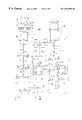
- FIG. 3is a block diagram representation of a shared functional block CDMA-1900 and GSM-900 communication transceiver according to an embodiment of the present invention.
- FIG. 4is a block diagram representation of a shared functional block CDMA-900 and GSM-900 communication transceiver according to an embodiment of the present invention.
- FIG. 5is a block diagram representation of a shared functional block CDMA-1900 and PCS communication transceiver according to an embodiment of the present invention.
- FIG. 6is a block diagram representation of a shared functional block CDMA-1900 and PCS communication transceiver according to an embodiment of the present invention.
- GSM communication standardsemploy several different communication standards worldwide and utilize several different frequency bands.
- the GSM communication standardoperates over three different bands, 900 MHz, 1800 MHz, and 1900 MHz
- the CDMA communication standardoperates over two different bands, 900 MHz and 1900 MHz.
- Multi-mode, multi-band cellular telephoneswith the flexibility to operate under multiple communications standards, afford consumers widespread applicability and allow manufacturers to benefit from the cost-efficiency of a common design.
- Embodiments of the present inventiontherefore relate to multi-mode, multi-band cellular communication transceivers that share frequency sources, amplifiers, and mixers between bands and modes. It should be noted, however, that transceivers according to embodiments of the present invention are not unique to cellular communications and may be employed in a variety of communications electronics, including wireless transmission systems as well as wired systems. Thus, embodiments of the invention described herein may involve various forms of communications systems.
- personal wireless communications systemsincluding, but not limited to digital mobile telephones, digital cordless telephones, digital pagers, combinations thereof, and the like.
- personal communications systemstypically include one or more portable or remotely located receiver and/or transmitter units.
- embodiments of the present inventioncombine two communication modes, GSM and CDMA.
- CDMA-900frequency bands are allocated such that a mobile subscriber unit will transmit signals over a transmit band of about 824-849 MHz and receive signals over a receive band of about 869-894 MHz.
- CDMA-1900frequency bands are allocated such that a mobile subscriber unit will transmit signals over a transmit band of about 1850-1910 MHz and receive signals over a receive band of about 1930-1990 MHz.
- CDMA functional blocks employed in embodiments of the present inventionshould conform to Telecommunications Industry Association (TIA)/Electronic Industry Association (EIA)/Interim Standard (IS) “CDMA-900” (TIA/EIA/IS-95-A and TIA/EIA/IS-98-A), and American National Standards Institute, Inc. (ANSI) “CDMA-1900” (J-STD-018), standards that are well understood by those skilled in the art. These standards are incorporated herein by reference.
- GSMGlobal System for Mobile communications
- GSM-900frequency bands are allocated such that a mobile subscriber unit will transmit signals over a transmit band of between about 890 and 915 MHz and will receive signals over a receive band of between about 935 to 960 MHz.
- the transmit bandis broken up into 125 channels, each channel separated by 200 kHz.
- DCSfrequency bands are allocated such that a mobile subscriber unit will transmit signals over a transmit band of between about 1710 and 1785 MHz and will receive signals over a receive band of between about 1805 and 1880 MHz.
- the transmit bandis broken up into 375 channels, each channel separated by 200 kHz.
- GSM functional blocks employed in embodiments of the present inventionconform to European Telecommunications Standards Institute (ETSI) “GSM-900 & DCS-1800” (GSM 05.05, GSM 11.10-1, and TBR 5 ) and American National Standards Institute, Inc. (ANSI) “GSM-1900” (J-STD-007 Volumes 0-7), standards that are well understood by those skilled in the art. These standards are incorporated herein by reference.
- embodiments of the present inventioninclude the following GSM/CDMA combinations: CDMA-900 and CSM-900, CDMA-900 and DCS, CDMA-900 and PCS, CDMA-1900 and CSM-900, CDMA-1900 and DCS, and CDMA-1900 and PCS.
- GSM/CDMA combinationsCDMA-900 and CSM-900, CDMA-900 and DCS, CDMA-900 and PCS, CDMA-1900 and CSM-900, CDMA-1900 and DCS, and CDMA-1900 and PCS.
- the illustrated embodimentsare limited to dual-mode, dual-band transceivers
- alternative embodiments of the present inventioninclude multi-mode, multi-band transceivers such as a combined CDMA-1900, PCS, and DCS transceiver.
- the PCS and DCS transmit and receive pathsmay contain paralleled filters to accommodate the relatively slight frequency differences between PCS and DCS.
- FIG. 1A generalized representation of a communication system according to an embodiment of the present invention is shown in FIG. 1, wherein a transceiver 10 includes a transmitting unit 12 and a receiving unit 14 , coupled for communication over a communication channel 42 .
- Transmitting unit 12includes a modulator 16 coupled to receive a transmit baseband information signal 18 from a signal source (not shown in FIG. 1 ).
- the signal sourcemay include, for example, a microphone for converting sound waves into electronic signals and sampling and analog-to-digital converter electronics for sampling and converting the electronic signals into digital signals representative of the sound waves.
- the signal sourcemay include any suitable device for producing digital data signals for communication over channel 42 , such as, but not limited to, a keyboard, a digital voice encoder, a mouse or other user input device, a sensor, monitor or testing apparatus, or the like.
- Modulator 16provides a transmit IF information signal 32 as an output to a transmitter 20 .
- a transmit RF information signal 26is produced by transmitter 20 for transmission from an antenna 22 .
- Receiving unit 14includes a receiver 24 coupled to an antenna 22 to process a receive RF information signal 44 .
- Receiver 24provides a modulated receive IF information signal 34 to a demodulator 28 , which demodulates receive IF information signal 34 and generates receive baseband information signals 46 .
- the demodulated receive baseband information signals 46 from demodulator 28may be provided to signal processing electronics, sound producing electronics or the like, depending upon the nature of use of the transceiver 10 .
- the transmitting and receiving units 12 and 14include further components, power supplies, and the like, well known in the art for effecting transmission and reception of signals and for carrying out other functions specific to the nature and application of use of the transceiver 10 .
- each transmitting unit 12 and receiving unit 14is configured to function as both a transmitting unit and a receiving unit.
- transmitting unit 12 and receiving unit 14transmit and receive signals directly therebetween.
- transmitting unit 12 and receiving unit 14communicate through one or more additional transceiver stations 30 (such as repeaters, base or cell stations, or the like).
- baseband information signal 18provides sampled voice (or sound) signals in the form of baseband I and Q channel signals to an encoder 36 .
- encoder 36comprises a Phase Shift Key encoder, such as, but not limited to, a ⁇ /4-shift Quadrature Phase Shift Key mapper with differential encoder ( ⁇ /4 DQPSK), and shaping filters 38 comprise pulse shaping filters for smoothing the encoder output signal.
- ⁇ /4 DQPSK and pulse shaping electronicsAn example of a ⁇ /4 DQPSK and pulse shaping electronics is described in the article titled: “ ⁇ /4-shift QPSK Digital Modulator LSIC for Personal Communication Terminals,” by Tetsu Sakata, Kazuhiko Seki, Shuji Kubota and Shuzo Kato, Proc. 5th IEEE International Symposium on Personal, Indoor and Mobile Radio Communications, 1994 (incorporated herein by reference).
- Other embodimentsmay employ other suitable encoding schemes, including but not limited to Amplitude Shift Keying and Frequency Shift Keying schemes.
- I and Q outputs of the encoderpass through shaping filters 38 and then to frequency conversion and modulation electronics 40 , the output of which comprises a transmit IF information signal 32 .
- Transmit IF information signal 32is then fed to transmitter 20 as shown in FIG. 1, which provides the transmit RF information signal 26 to the antenna 22 for transmission.
- FIG. 3A shared functional block CDMA-1900 and CSM-900 communication transceiver 48 according to an embodiment of the present invention is illustrated in FIG. 3 .
- the transceiver 48includes a modulator 16 as described above with reference to FIG. 2 .
- frequency conversion and modulation electronics 40receive the I and Q outputs of shaping filters 38 and modulate a transmit IF LO 50 with the I and Q outputs to produce a transmit IF information signal 32 at an IF carrier frequency.
- Transmit IF LO 50is generated by a transmit IF LO frequency generator 52 comprising a CDMA transmit IF LO frequency source 54 phase-locked to a reference source 58 by transmit IF LO loop electronics 56 .
- CDMA transmit IF LO frequency source 54is a voltage controlled oscillator (VCO).
- VCOvoltage controlled oscillator
- CDMA transmit IF LO frequency source 54may be any adjustable frequency source.
- Transmit IF information signal 32is then amplified by a transmit IF variable gain amplifier (VGA) 60 within transmitter 20 , which adjusts its gain based on commands received from the base station.
- VGAtransmit IF variable gain amplifier
- a variable gain amplifieris not required for GSM, power control is critical in CDMA, and thus because transmit IF VGA 60 is shared between the CDMA and GSM receive paths, transmit IF VGA 60 must have variable gain capability to meet the power control requirements of CDMA.
- the output of transmit IF VGA 60is split by first transmit IF power splitter 208 , and in the CDMA-1900 transmit path is then filtered by CDMA transmit IF filter 62 , which filters out noise generated by the transmit IF VGA 60 in the receive band to meet receive band noise floor requirements.
- CDMA transmit IF filter 62has a center frequency approximately equivalent to the IF carrier frequency and a bandwidth sufficient to pass the modulated and amplified transmit IF information signal with minimal distortion.
- CDMAhas a modulation bandwidth of 1.25 MHz, thus the bandwidth of CDMA transmit IF filter 62 must be at least 1.25 MHz. In preferred embodiments, the bandwidth of CDMA transmit IF filter 62 is about 5 MHz.
- CDMA transmit upconverter mixer 66The modulated, amplified, and filtered transmit IF information signal is then mixed with a CDMA transmit RF LO 64 in CDMA transmit upconverter mixer 66 .
- CDMA transmit upconverter mixer 66generates the difference between the output of CDMA transmit IF filter 62 and CDMA transmit RF LO 64 .
- CDMA transmit RF LO 64is generated by a CDMA RF LO frequency generator 68 containing a CDMA RF LO frequency source 70 phase-locked to reference source 58 by CDMA RF LO loop electronics 72 .
- CDMA RF LO frequency source 70comprises a VCO.
- CDMA RF LO frequency source 70may be any adjustable frequency source.
- the output of CDMA transmit upconverter mixer 66is filtered by first CDMA transmit RF filter 74 which, in the CDMA-1900 example of FIG. 3, has a passband encompassing the CDMA-1900 transmit band of about 1850-1910 MHz to remove spurious frequencies generated by CDMA transmit upconverter mixer 66 .
- the output of first CDMA transmit RF filter 74is then amplified by CDMA transmit RF driver amplifier 76 .
- the output of CDMA transmit RF driver amplifier 76is then filtered by second CDMA transmit RF filter 78 , which in the CDMA-1900 example of FIG.
- CDMA transmit RF information signal 26is then filtered by duplexer 82 , which in the CDMA-1900 example of FIG. 3 has a transmit passband encompassing the CDMA-1900 transmit band of about 1850-1910 MHz to filter out-of-band noise generated by CDMA transmit RF power amplifier 80 .
- mode select switch 84may be an RF switch, a resistor combiner, or a duplexer.
- signals from antenna 22enter antenna coupling electronics 86 , where they pass through mode select switch 84 and are filtered by duplexer 82 having a receive passband approximately equivalent to the CDMA-1900 receive band of about 1930-1990 MHz for passing only CDMA-1900 receive band signals.
- the output of duplexer 82is CDMA receive RF information signal 88 .
- CDMA receive RF information signal 88is then amplified by a CDMA receive RF LNA 90 .
- the output of CDMA receive RF LNA 90is then filtered by a CDMA receive RF image reject filter 92 .
- CDMA receive RF image reject filter 92is a bandpass filter with a passband approximately equivalent to the CDMA-1900 receive band of about 1930-1990 MHz to filter out image noise generated by CDMA receive RF LNA 90 capable of mixing with CDMA receive RF LO 94 in CDMA receive downconverter mixer 96 and producing unwanted signals in the IF band.
- CDMA receive RF LO 94is generated by CDMA RF LO frequency generator 68 , and CDMA receive downconverter mixer 96 generates the difference between the output of CDMA receive RF image reject filter 92 and CDMA receive RF LO 94 , designated herein as CDMA receive IF information signal 102 .
- active image cancellationsuch as an image reject mixer may be employed, eliminating the need for CDMA receive RF image reject filter 92 .
- CDMA receive IF information signal 102then passes through a CDMA receive IF filter 98 with a bandwidth approximately equivalent to the CDMA modulation bandwidth of 1.25 MHz to remove spurious frequencies generated by CDMA receive downconverter mixer 96 .
- the output of CDMA receive IF filter 98is then coupled to receive IF VGA 100 through a first receive IF switch 206 .
- Receive IF VGA 100provides variable gain control by adjusting its gain based on commands received from the base station.
- the output of receive IF VGA 100is receive IF information signal 34 .
- Receive IF information signal 34is mixed with receive IF LO 116 and demodulated by frequency conversion and demodulation electronics 104 within demodulator 28 .
- receive IF LO 116is generated by a receive IF LO frequency generator 112 comprising a CDMA receive IF LO frequency source 110 phase-locked to reference source 58 by receive IF LO loop electronics 114 .
- CDMA receive IF LO frequency source 110is a VCO.
- CDMA receive IF LO frequency source 110may be any adjustable frequency source.
- Frequency conversion and demodulation electronics 104produce baseband information signals 120 , characterized herein as either DC or a “near DC” IF (for example, a center frequency above about 1 MHz).
- these baseband information signals 120are filtered by CDMA baseband filters 106 to remove spurious frequencies generated by frequency conversion and demodulation electronics 104 .
- CDMA baseband filters 106have a bandwidth of about 1.25 MHz to accommodate the modulation bandwidth of CDMA receive baseband signals, and may be low pass filters if the receive baseband signals are DC, or bandpass filters if the receive baseband signals are near DC.
- the filtered and demodulated receive baseband signalsare then processed by quantizers 108 , which generate CDMA I and Q outputs 122 .
- quantizers 108are analog-to-digital converters (ADCs).
- the CSM-900 transmit pathshares modulator 16 and transmit IF VGA 60 with the CDMA-1900 transmit path.
- transmit IF LO 50used by frequency conversion and modulation electronics 40 to generate transmit IF information signal 32 , is produced by GSM transmit IF LO frequency source 126 within transmit IF LO frequency generator 52 .
- GSM transmit IF LO frequency source 126is coupled in parallel with CDMA transmit IF LO frequency source 54 and is phase-locked to reference source 58 by transmit IF LO loop electronics 56 .
- the CSM-900 transmit pathdiverges from the CDMA-1900 transmit path at the output of transmit IF VGA 60 , where the output of transmit IF VGA 60 is split by first transmit IF power splitter 208 and filtered by GSM transmit IF filter 128 , which filters out noise generated by the transmit IF VGA 60 in the GSM receive band to meet receive band noise floor requirements.
- GSM transmit IF filter 128has a center frequency approximately equivalent to the:IF carrier frequency and a bandwidth sufficient to pass the modulated and amplified-transmit IF information signal with minimal distortion.
- GSMhas a modulation bandwidth of 200 kHz, thus the bandwidth of GSM transmit IF filter 128 must be at least 200 kHz. In preferred embodiments, the bandwidth of GSM transmit IF filter 128 is about 1 MHz.
- the output of GSM transmit IF filter 128is then upconverted by a translation loop 130 .
- translation loop 130includes a GSM VCO 132 coupled to a translation loop mixer 134 and phase-locked to a GSM transmit RF LO 136 for generating GSM RF carrier frequencies.
- Translation loop 130acts like a tracking filter with a center. frequency at the frequency of the GSM VCO 132 .
- GSM transmit RF LO 136is generated by a GSM RF LO frequency generator 138 comprising a GSM RF LO frequency source 140 phase-locked to reference source 58 by GSM RF LO loop electronics 142 .
- GSM RF LO frequency source 140comprises a VCO.
- GSM RF LO frequency source 140may be any adjustable frequency source.
- translation loop mixer 134generates the difference between GSM VCO 132 and GSM transmit RF LO 136 .
- Translation loop 130further includes a feedback filter 144 for filtering the output of translation loop mixer 134 to remove mixer noise, a phase detector 146 for determining the phase difference between the output of feedback filter 144 and GSM transmit IF filter 128 , a charge pump 148 for sourcing or sinking current as determined by the phase difference output of phase detector 146 , and a loop filter 150 for integrating current pulses from charge pump 148 and providing a control voltage 152 to GSM VCO 132 .
- the modulated, upconverted output of GSM VCO 132is then amplified by GSM transmit RF power amplifier 154 to generate a GSM transmit RF information signal at a level sufficient to meet output power requirements at antenna 22 .
- the output of GSM transmit RF power amplifier 154is then filtered by GSM transmit RF filter 156 , which in the CSM-900 example of FIG. 3 has a transmit passband encompassing the CSM-900 transmit band of about 890-915 MHz to filter out-of-band noise generated by GSM transmit RF power amplifier 154 .
- GSM transmit RF filter 156identified herein as GSM transmit RF information signal 204 , then passes through transmit/receive switch 158 within antenna coupling electronics 86 and mode select switch 84 before being transmitted by antenna 22 .
- transmit/receive switch 158may be an RF switch, a resistor combiner, or a duplexer.
- translation loop 130 in the GSM transmit pathgenerates a relatively clean (minimal out-of-band noise) signal from GSM VCO 132 , there is no need for a high-insertion loss duplexer, as used in the CDMA transmit path.
- the elimination of the duplexerenables a lower power GSM transmit RF power amplifier to be used, resulting in substantial power savings in the communication transceiver.
- the CDMA transmit pathcannot use a translation loop, however, because a translation loop cannot track the amplitude information present in a CDMA Offset QPSK (OQPSK) signal.
- OFPSKCDMA Offset QPSK
- translation loop 130may be replaced by an upconverter mixer as in the CDMA transmit path.
- transmit/receive switch 158may be replaced with a duplexer to filter out-of-band noise generated by GSM transmit RF power amplifier 154 .
- signals from antenna 22enter antenna coupling electronics 86 , where they pass through mode select switch 84 and transmit/receive switch 158 .
- the output of transmit/receive switch 158is GSM receive RF information signal 162 , which is filtered by preselector filter 164 having a receive passband approximately equivalent to the CSM-900 receive band of about 935-960 MHz for passing only CSM-900 receive band signals.
- GSM receive RF LNA 166The output of preselector filter 164 is then amplified by a GSM receive RF LNA 166 .
- the output of GSM receive RF LNA 166is then filtered by a GSM receive RF image reject filter 168 .
- GSM receive RF image reject filter 168is a bandpass filter with a bandwidth approximately equivalent to the CSM-900 receive band of about 935-960 MHz to filter out image noise generated by GSM receive RF LNA 166 capable of mixing with GSM receive RF LO 170 in GSM receive downconverter mixer 172 and producing unwanted signals in the IF band.
- GSM receive RF LO 170is generated by GSM RF LO frequency generator 138 , and GSM receive downconverter mixer 172 generates the difference between the output of GSM receive RF image reject filter 168 and GSM receive RF LO 170 , designated herein as GSM receive IF information signal 174 .
- active image cancellationsuch as an image reject mixer may be employed, eliminating the need for GSM receive RF image reject filter 168 .
- GSM receive IF information signal 174then passes through a GSM receive IF filter 176 with a bandwidth approximately equivalent to the GSM modulation bandwidth of 200 kHz to remove spurious frequencies generated by GSM receive downconverter mixer 172 .
- the output of GSM receive IF filter 176is then coupled to receive IF VGA 100 by first receive IF switch 206 , where it is amplified by receive IF VGA 100 .
- the output of CDMA receive IF filter 98is also coupled to receive IF VGA 100 by first receive IF switch 206 .
- the gain, NF, and IIP 3 of the shared receive IF VGA 100must be chosen to satisfy the requirements of both the CDMA-1900 and CSM-900 receive paths.
- first receive IF switch 206may comprise a switchable high off-state impedance buffer amplifiers or an RF switch.
- Receive IF information signal 34is then mixed with receive IF LO 116 and demodulated by frequency conversion and demodulation electronics 104 within demodulator 28 . Because the IF frequencies of CDMA-1900 and CSM-900 may be different, receive IF LO 116 as used for GSM demodulation is not generated by CDMA receive IF LO frequency source 110 . Instead, receive IF LO 116 as used for GSM demodulation is generated by a GSM receive IF LO frequency source 160 in parallel with CDMA receive IF LO frequency source 110 and phase-locked to reference source 58 by receive IF LO loop electronics 114 . In preferred embodiments of the present invention, GSM receive IF LO frequency source 160 is a VCO. However, in alternative embodiments, GSM receive IF LO frequency source 160 may be any adjustable frequency source.
- Frequency conversion and demodulation electronics 104produce baseband information signals 120 .
- these baseband information signals 120are filtered by GSM baseband filters 118 to remove spurious frequencies generated by frequency conversion and demodulation electronics 104 .
- GSM baseband filters 118have a bandwidth of about 200 kHz to accommodate the modulation bandwidth of GSM receive baseband signals, and may be low pass filters if the receive baseband signals are DC, or bandpass filters if the receive baseband signals are near DC.
- the filtered and demodulated receive baseband signalsare then processed by quantizers 108 , which generate GSM I and Q outputs 124 .
- quantizers 108are analog-to-digital converters (ADCs).
- mode selector electronics 178configures the CDMA-1900 and CSM-900 communication transceiver 48 for either CDMA or GSM operation.
- mode selector electronics 178is a processing device automatically configurable by remote commands or signal strength measurements received from base stations.
- mode selector electronics 178may comprise a factory-programmable logic device or user-configurable logic.
- mode select switch 84is configured to couple duplexer 82 to antenna 22
- receive IF LO frequency generator 112is configured to couple CDMA receive IF LO frequency source 110 to frequency conversion and demodulation electronics 104
- transmit IF LO frequency generator 52is configured to couple CDMA transmit IF LO frequency source 54 to frequency conversion and modulation electronics 40 .
- mode select switch 84is configured to couple transmit/receive switch 158 to antenna 22
- receive IF LO frequency generator 112is configured to couple GSM receive IF LO frequency source 160 to frequency conversion and demodulation electronics 104
- transmit IF LO frequency generator 52is configured to couple GSM transmit IF LO frequency source 126 to frequency conversion and modulation electronics 40 .
- Embodiments of the present invention described aboveemploy a separate CDMA transmit IF LO frequency source 54 and GSM transmit IF LO frequency source 126 .
- CDMA transmit IF LO frequency source 54 and GSM transmit IF LO frequency source 126may comprise a single tunable transmit IF LO frequency source.
- embodiments of the present invention described abovedisclose a separate CDMA receive IF LO frequency source 110 and GSM receive IF LO frequency source 160 .
- CDMA receive IF LO frequency source 110 and GSM receive IF LO frequency source 160may comprise a single tunable receive IF LO frequency source.
- embodiments of the present invention described aboveemploy a single CDMA RF LO frequency source 70 .
- CDMA RF LO frequency source 70may comprise a separate CDMA receive RF LO frequency source and a separate CDMA transmit RF LO frequency source.
- embodiments of the present invention described abovedisclose a single GSM RF LO frequency source 140 .
- GSM RF LO frequency source 140may comprise a separate GSM receive RF LO frequency source and a separate GSM transmit RF LO frequency source.
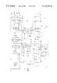
- FIG. 4A shared functional block CDMA-900 and CSM-900 communication transceiver 180 according to an embodiment of the present invention is illustrated in FIG. 4 .
- the architecture and operation of CDMA-900 and CSM-900 communication transceiver 180 in FIG. 4is similar to that of CDMA-1900 and CSM-900 communication transceiver 48 in FIG. 3, except as noted below.
- CDMA receive RF information signal 88passes through a variable gain attenuator 182 in preferred embodiments of the present invention.
- variable gain attenuator 182selectively attenuates the received signal to meet CDMA communication standard cellular receive band intermodulation requirements.
- attenuation controlmay be achieved by selectively bypassing common receive RF LNA 184 , or a variable gain common receive RF LNA 184 may be employed instead of variable gain attenuator 182 .
- variable gain attenuator 182 in the CDMA receive path and preselector filter 164 in the GSM receive pathare coupled by a first receive RF switch 186 , which, in alternative embodiments of the present invention, may be an RF switch, high off-state impedance amplifiers or transmission gates, a resistor combiner, or a duplexer.
- First receive RF switch 186allows common receive RF LNA 184 to be used in both the CDMA and GSM receive paths.
- the use of a single, limited frequency range LNAis possible in CDMA-900 and CSM-900 communication transceiver 180 because the frequency bands of CDMA-900 and CSM-900 are similar.
- common receive RF LNA 184is shared between the CDMA-900 and CSM-900 receive paths, the gain, NF, and IIP 3 of common receive RF LNA 184 must be chosen to satisfy the requirements of both the CDMA-900 and CSM-900 receive paths.
- the output of common receive RF LNA 184is then coupled to either CDMA receive RF image reject filter 92 or GSM receive RF image reject filter 168 by second receive RF switch 188 .
- second receive RF switch 188may be an RF switch, high off-state impedance amplifiers or transmission gates, a resistor combiner, or a duplexer.
- CDMA receive RF image reject filter 92 and GSM receive RF image reject filter 168are then coupled to common receive downconverter mixer 190 by third receive RF switch 192 .
- Third receive RF switch 192allows common receive downconverter mixer 190 to be used in both the CDMA and GSM receive paths, which is possible because of the small frequency difference between the receive bands of CDMA-900 and CSM-900. Because common receive downconverter mixer 190 is shared between the CDMA-900 and CSM-900 receive paths, the gain, NF, and IIP 3 of common receive downconverter mixer 190 must be chosen to satisfy the requirements of both the CDMA-900 and CSM-900 receive paths.
- third receive RF switch 192may be an RF switch, high off-state impedance amplifiers or transmission gates, a resistor combiner, or a duplexer.
- Downconverter mixer 190mixes either the output of CDMA receive RF image reject filter 92 or the output of GSM receive RF image reject filter 168 with a common receive RF LO 194 .
- Common receive RF LO 194is produced by coupling CDMA RF LO frequency source 70 and GSM RF LO frequency source 140 with a common receive RF LO power combiner 200 .
- the output of common receive RF LO power combiner 200is approximately equivalent to either the output of CDMA RF LO frequency source 70 or the output of GSM RF LO frequency source 140 , because mode selector electronics 178 enables either CDMA RF LO frequency source 70 or GSM RF LO frequency source 140 , but not both.
- the output of downconverter mixer 190is coupled to CDMA receive IF filter 98 and GSM receive IF filter 176 through common receive IF power splitter 202 , which distributes a signal approximately equal in amplitude and phase to CDMA receive IF filter 98 and GSM receive IF filter 176 .
- CDMA receive IF filter 98 and GSM receive IF filter 176are surface acoustic wave (SAW) filters, because SAW filters act as high impedance elements for out-of-band frequencies.
- SAWsurface acoustic wave
- the outputs of CDMA receive IF filter 98 and GSM receive IF filter 176are coupled to receive IF VGA 100 by first receive IF switch 206 . Because receive IF VGA 100 is shared between the CDMA-900 and CSM-900 receive paths, the gain, NF, and IIP 3 of receive IF VGA 100 must be chosen to satisfy the requirements of both the CDMA-900 and CSM-900 receive paths.
- first receive RF switch 186is configured to couple variable gain attenuator 182 to common receive RF LNA 184
- second receive RF switch 188is configured to couple common receive RF LNA 184 to CDMA receive RF image reject filter 92
- third receive RF switch 192is configured to couple CDMA receive RF image reject filter 92 to common to receive downconverter mixer 190 .
- first receive RF switch 186is configured to couple preselector filter 164 to common receive RF LNA 184
- second receive RF switch 188is configured to couple common receive RF LNA 184 to GSM receive RF image reject filter 168
- third receive RF switch 192is configured to couple GSM receive RF image reject filter 168 to common receive downconverter mixer 190 .
- RF filters in the CDMA transmit and receive paths of CDMA-900 and CSM-900 communication transceiver 180have different passbands as compared to those in FIG. 3 .
- First CDMA transmit RF filter- 74 , second CDMA transmit RF filter 78 , and duplexer 82have transmit passbands encompassing the CDMA-900 transmit band of about 824-849 MHz.
- Duplexer 82 and CDMA receive RF image reject filter 92have receive passbands approximately equivalent to the CDMA-900 receive band of about 869-894 MHz.
- FIG. 5A shared functional block CDMA-900 and PCS communication transceiver 196 according to an embodiment of the present invention is illustrated in FIG. 5 . It should be noted that a similar architecture is applicable to a shared functional block CDMA-900 and DCS communication transceiver.
- the architecture and operation of CDMA-900 and PCS communication transceiver 196 in FIG. 5is similar to that of CDMA-1900 and CSM-900 communication transceiver 48 in FIG. 3, except that in the CDMA receive path, variable gain attenuator 182 is coupled between duplexer 82 and CDMA receive RF LNA 90 . Note that because receive IF VGA 100 is shared by the CDMA-900 and PCS receive paths, the gain, NF, and IIP 3 of the shared receive IF VGA 100 must be chosen to satisfy the requirements of both the CDMA-900 and PCS receive paths.
- First CDMA transmit RF filter 74 , second CDMA transmit RF filter 78 , and duplexer 82have transmit passbands encompassing the CDMA-900 transmit band of about 824-849 MHz.
- Duplexer 82 and CDMA receive RF image reject filter 92have receive passbands approximately equivalent to the CDMA-900 receive band of about 869-894 MHz.
- GSM transmit RF filter 156has a transmit passband encompassing the PCS transmit band of about 1850-1910 MHz.
- Preselector filter 164 and GSM receive RF image reject filter 168have receive passbands approximately equivalent to the PCS receive band of about 1930-1990 MHz.
- GSM transmit RF filter 156has a transmit passband encompassing the DCS transmit band of about 1710-1785 MHz, and preselector filter 164 and GSM receive RF image reject filter 168 have receive passbands approximately equivalent to the DCS receive band of about 1805-1880 MHz.
- FIG. 6A shared functional block CDMA-1900 and PCS communication transceiver 198 according to an embodiment of the present invention is illustrated in FIG. 6 . It should be noted that a similar architecture is applicable to a shared functional block CDMA-1900 and DCS communication transceiver. The architecture and operation of CDMA-1900 and PCS communication transceiver 198 in FIG. 6 is similar to that of CDMA-1900 and CSM-900 communication transceiver 48 in FIG.
- first receive RF switch 186which, in alternative embodiments of the present invention, may be an RF switch, high off-state impedance amplifiers or transmission gates, a resistor combiner, or a duplexer.
- First receive RF switch 186allows common receive RF LNA 184 to be used in both the CDMA and GSM receive paths. The use of a single, limited frequency range LNA is possible in CDMA-1900 and PCS communication transceiver 198 because the frequency bands of CDMA-1900 and PCS are similar.
- common receive RF LNA 184is shared between the CDMA-1900 and PCS receive paths, the gain, NF, and IIP 3 of common receive RF LNA 184 must be chosen to satisfy the requirements of both the CDMA-1900 and PCS receive paths.
- the output of common receive RF LNA 184is then coupled to either CDMA receive RF image reject filter 92 or GSM receive RF image reject filter 168 by second receive RF switch 188 .
- second receive RF switch 188may be an RF switch, high off-state impedance amplifiers or transmission gates, a resistor combiner, or a duplexer.
- CDMA receive RF image reject filter 92 and GSM receive RF image reject filter 168are then coupled to common receive downconverter mixer 190 by third receive RF switch 192 .
- Third receive RF switch 192allows common receive downconverter mixer 190 to be used in both the CDMA and GSM receive paths, which is possible because of the small frequency difference between the receive bands of CDMA-1900 and PCS. Because common receive downconverter mixer 190 is shared between the CDMA-1900 and PCS receive paths, the gain, NF, and IIP 3 of common receive downconverter mixer 190 must be chosen to satisfy the requirements of both the CDMA-1900 and PCS receive paths.
- third receive RF switch 192may be an RF switch, high off-state impedance amplifiers or transmission gates, a resistor combiner, or a duplexer.
- Downconverter mixer 190mixes either the output of CDMA receive RF image reject filter 92 or the output of GSM receive RF image reject filter 168 with a common receive RF LO 194 .
- Common receive RF LO 194is produced by coupling CDMA RF LO frequency source 70 and GSM RF LO frequency source 140 with a common receive RF LO power combiner 200 .
- the output of common receive RF LO power combiner 200is approximately equivalent to either the output of CDMA RF LO frequency source 70 or the output of GSM RF LO frequency source 140 , because mode selector electronics 178 enables either CDMA RF LO frequency source 70 or GSM RF LO frequency source 140 , but not both.
- the output of downconverter mixer 190is coupled to CDMA receive IF filter 98 and GSM receive IF filter 176 through common receive IF power splitter 202 , which distributes a signal approximately equal in amplitude and phase to CDMA receive IF filter 98 and GSM receive IF filter 176 .
- CDMA receive IF filter 98 and GSM receive IF filter 176are surface acoustic wave (SAW) filters, because SAW filters act as high impedance elements for out-of-band frequencies.
- SAWsurface acoustic wave
- the outputs of CDMA receive IF filter 98 and GSM receive IF filter 176are coupled to receive IF VGA 100 by first receive IF filter 206 . Because receive IF VGA 100 is shared between the CDMA-1900 and PCS receive paths, the gain, NF, and IIP 3 of receive IF VGA 100 must be chosen to satisfy the requirements of both the CDMA-1900 and PCS receive paths.
- first receive RF switch 186is configured to couple duplexer 82 to common receive RF LNA 184
- second receive RF switch 188is configured to couple common receive RF LNA 184 to CDMA receive RF image reject filter 92
- third receive RF switch 192is configured to couple CDMA receive RF image reject filter 92 to common receive downconverter mixer 190 .
- first receive RF switch 186is configured to couple preselector filter 164 to common receive RF LNA 184
- second receive RF switch 188is configured to couple common receive RF LNA 184 to GSM receive RF image reject filter 168
- third receive RF switch 192is configured to couple GSM receive RF image reject filter 168 to common receive downconverter mixer 190 .
- GSM transmit RF filter 156has a transmit passband encompassing the PCS transmit band of about 1850-1910 MHz, and preselector filter 164 and GSM receive RF image reject filter 168 have receive passbands approximately equivalent to the PCS receive band of about 1930-1990 MHz.
- GSM transmit RF filter 156has a transmit passband encompassing the DCS transmit band of about 1710-1785 MHz, and preselector filter 164 and GSM receive RF image reject filter 168 have receive passbands approximately equivalent to the DCS receive band of about 1805-1880 MHz.
- FIGS. 3-6illustrate embodiments of the present invention which utilize modulation to, and demodulation from, an IF frequency
- direct conversionmay be employed.
- receive RF information signalsare downconverted and demodulated directly to baseband
- baseband information signalsare modulated and upconverted directly to transmit RF information signals.
- preferred embodiments of the present inventionprovide a system and process for a multi-mode, multi-band CDMA and GSM communication transceiver that shares frequency sources, amplifiers, and mixers between transmitters and receivers and between bands to minimize size, weight, complexity, power consumption, and cost.
Landscapes
- Engineering & Computer Science (AREA)
- Computer Networks & Wireless Communication (AREA)
- Signal Processing (AREA)
- Transceivers (AREA)
- Mobile Radio Communication Systems (AREA)
- Transmitters (AREA)
- Circuits Of Receivers In General (AREA)
Abstract
Description
Claims (17)
Priority Applications (10)
| Application Number | Priority Date | Filing Date | Title |
|---|---|---|---|
| US09/298,315US6584090B1 (en) | 1999-04-23 | 1999-04-23 | System and process for shared functional block CDMA and GSM communication transceivers |
| EP00925948AEP1175733B1 (en) | 1999-04-23 | 2000-04-12 | System and process for shared functional block cdma and gsm communication transceivers |
| DE60026020TDE60026020T2 (en) | 1999-04-23 | 2000-04-12 | SYSTEM AND METHOD FOR COMMON FUNCTION BLOCKS IN CDMA AND GSM SEND RECEIVERS |
| DK00925948TDK1175733T3 (en) | 1999-04-23 | 2000-04-12 | System and method for CDMA and GSM communication transceivers with common function blocks |
| KR1020017013580AKR100646485B1 (en) | 1999-04-23 | 2000-04-12 | System and process for shared function block CDA and EMS communication transceivers |
| JP2000614568AJP4494650B2 (en) | 1999-04-23 | 2000-04-12 | System and process for shared functional block CDMA / GSM communication transceiver |
| AT00925948TATE318022T1 (en) | 1999-04-23 | 2000-04-12 | SYSTEM AND METHOD FOR COMMON FUNCTIONAL BLOCKS IN CDMA AND GSM TRANSCEIVERS |
| PCT/US2000/009841WO2000065734A1 (en) | 1999-04-23 | 2000-04-12 | System and process for shared functional block cdma and gsm communication transceivers |
| TW089107594ATW466838B (en) | 1999-04-23 | 2000-05-16 | System and process for shared functional block CDMA and GSM communication transceivers |
| US10/444,803US7092676B2 (en) | 1999-04-23 | 2003-05-23 | Shared functional block multi-mode multi-band communication transceivers |
Applications Claiming Priority (1)
| Application Number | Priority Date | Filing Date | Title |
|---|---|---|---|
| US09/298,315US6584090B1 (en) | 1999-04-23 | 1999-04-23 | System and process for shared functional block CDMA and GSM communication transceivers |
Related Child Applications (1)
| Application Number | Title | Priority Date | Filing Date |
|---|---|---|---|
| US10/444,803Continuation-In-PartUS7092676B2 (en) | 1999-04-23 | 2003-05-23 | Shared functional block multi-mode multi-band communication transceivers |
Publications (1)
| Publication Number | Publication Date |
|---|---|
| US6584090B1true US6584090B1 (en) | 2003-06-24 |
Family
ID=23149978
Family Applications (2)
| Application Number | Title | Priority Date | Filing Date |
|---|---|---|---|
| US09/298,315Expired - LifetimeUS6584090B1 (en) | 1999-04-23 | 1999-04-23 | System and process for shared functional block CDMA and GSM communication transceivers |
| US10/444,803Expired - LifetimeUS7092676B2 (en) | 1999-04-23 | 2003-05-23 | Shared functional block multi-mode multi-band communication transceivers |
Family Applications After (1)
| Application Number | Title | Priority Date | Filing Date |
|---|---|---|---|
| US10/444,803Expired - LifetimeUS7092676B2 (en) | 1999-04-23 | 2003-05-23 | Shared functional block multi-mode multi-band communication transceivers |
Country Status (9)
| Country | Link |
|---|---|
| US (2) | US6584090B1 (en) |
| EP (1) | EP1175733B1 (en) |
| JP (1) | JP4494650B2 (en) |
| KR (1) | KR100646485B1 (en) |
| AT (1) | ATE318022T1 (en) |
| DE (1) | DE60026020T2 (en) |
| DK (1) | DK1175733T3 (en) |
| TW (1) | TW466838B (en) |
| WO (1) | WO2000065734A1 (en) |
Cited By (37)
| Publication number | Priority date | Publication date | Assignee | Title |
|---|---|---|---|---|
| US20020001293A1 (en)* | 2000-05-17 | 2002-01-03 | Jong-Ho Kim | CDMA 3X base transceiver station in mobile communication system |
| US20020186713A1 (en)* | 2000-03-21 | 2002-12-12 | Dominique Brunel | Communication system with frequency modulation and a single local oscillator |
| US20030003886A1 (en)* | 2001-06-21 | 2003-01-02 | Kabushiki Kaisha Toshiba | Radio transmission apparatus and radio transmission method |
| US20030099215A1 (en)* | 2001-11-26 | 2003-05-29 | O'shea Helena | Reducing handover frequency error |
| US20030114128A1 (en)* | 2001-12-17 | 2003-06-19 | Nokia Corporation, Espoo Finland (2) | Method and apparatus for reducing RF filter induced distortion in a wide bandwidth wireless system by the use of channel-dependent RF filter compensation |
| US20030114121A1 (en)* | 2001-12-19 | 2003-06-19 | Alps Electric Co., Ltd. | Transmitter circuit for mobile telephone set compatible with two different systems |
| US20030193923A1 (en)* | 1999-04-23 | 2003-10-16 | Abdelgany Mohyeldeen Fouad | Shared functional block multi-mode multi-band communication transceivers |
| US20030235167A1 (en)* | 2002-06-25 | 2003-12-25 | Stephen Kuffner | Multiple mode RF communication device |
| US20040027197A1 (en)* | 2000-08-24 | 2004-02-12 | Howard Brian Butterfield | Power amplifier arrangement |
| US20040038659A1 (en)* | 2002-08-14 | 2004-02-26 | Nec Corporation | Automatic frequency control system, operation control method thereof and mobile communication device using the same |
| US20040116087A1 (en)* | 2002-12-10 | 2004-06-17 | Irf Semiconductor, Inc. | Radio frequency receiver architecture with on-chip tracking intermediate frequency filtering |
| US20040168193A1 (en)* | 2003-02-26 | 2004-08-26 | Kabushiki Kaisha Kenwood | Satellite digital radio broadcast receiver |
| US20050032493A1 (en)* | 2003-06-25 | 2005-02-10 | Hitachi, Ltd. | Multimode wireless terminal and wireless transmitter-receiver unit |
| US20050124351A1 (en)* | 2003-12-03 | 2005-06-09 | Black Greg R. | Method and apparatus for establishing direct mobile to mobile communication between cellular mobile terminals |
| US20060035599A1 (en)* | 2000-08-17 | 2006-02-16 | Kabushiki Kaisha Toshiba | Frequency synthesizer and multi-band radio apparatus using said frequency synthesizer |
| US20060121911A1 (en)* | 2004-12-08 | 2006-06-08 | Yan Zhang | Dummy PCH block detection for power saving in GSM handset |
| US20060141952A1 (en)* | 2003-01-06 | 2006-06-29 | Sirific Wireless Corporation | Multi-mode modulator and transmitter |
| US20060146917A1 (en)* | 2004-12-03 | 2006-07-06 | Kaoru Ishida | Multi-mode transmitter circuit for switching over between TDMA mode and CDMA mode |
| US20060274838A1 (en)* | 1998-08-10 | 2006-12-07 | Kamilo Feher | Agile RF band OFDM spread spectrum and cross-correlated systems |
| US20070036203A1 (en)* | 1998-08-10 | 2007-02-15 | Kamilo Feher | Processor, modulators and transceivers for spread spectrum, CDMA, CSMA, OFDM, TDM, TDMA cross correlated and filtered systems |
| US20070142080A1 (en)* | 2002-12-20 | 2007-06-21 | Renesas Technology Corp | Direct-conversion transmitter circuit and transceiver system |
| US7245651B1 (en)* | 1999-12-20 | 2007-07-17 | Intel Corporation | Dual mode filter for mobile telecommunications |
| US20070238483A1 (en)* | 2006-04-05 | 2007-10-11 | Olivier Boireau | Antenna sharing techniques |
| US20070281736A1 (en)* | 2006-04-28 | 2007-12-06 | Samsung Electronics Co., Ltd. | Apparatus for sharing CDMA scheme and Japanese CDMA scheme in communication system |
| US20080081577A1 (en)* | 2006-09-29 | 2008-04-03 | Ahmadreza Rofougaran | Method and system for utilizing diplexer/duplexer for wcdma operation as a filter for supporting gsm-based operation |
| US20080102885A1 (en)* | 2006-10-31 | 2008-05-01 | Jerome Tu | Coordination Among Multiple Co-Located Radio Modules |
| WO2008117972A1 (en)* | 2007-03-23 | 2008-10-02 | Hutech21 Co., Ltd. | M/w repeater using complex frequency band |
| US20090135781A1 (en)* | 1998-11-26 | 2009-05-28 | Nokia Corporation | Method and arrangement for transmitting and receiving rf signals through various radio interfaces of communication systems |
| US20090170447A1 (en)* | 2006-10-31 | 2009-07-02 | Palm, Inc. | Shared antenna architecture for multiple co-located radio modules |
| US20100048155A1 (en)* | 2007-01-19 | 2010-02-25 | Nec Electronics Corporation | Multi-band rf receiver |
| US20100227570A1 (en)* | 2009-03-09 | 2010-09-09 | Palm, Inc. | Isolation techniques for multiple co-located radio modules |
| US20120315950A1 (en)* | 2011-06-13 | 2012-12-13 | Chi Mei Communication Systems, Inc. | Dual mode mobile communication terminal |
| US8755747B2 (en) | 2006-10-31 | 2014-06-17 | Qualcomm Incorporated | Techniques to control transmit power for a shared antenna architecture |
| US9693390B2 (en) | 2009-06-01 | 2017-06-27 | Qualcomm Incorporated | Techniques to manage a mobile device based on network density |
| US20180294832A1 (en)* | 2017-04-10 | 2018-10-11 | Speedlink Technology Inc. | Wideband millimeter-wave frontend integrated circuit |
| CN113258942A (en)* | 2021-06-04 | 2021-08-13 | 上海创远仪器技术股份有限公司 | Demodulation device supporting all-system broadband communication signals |
| US11483779B2 (en)* | 2020-08-21 | 2022-10-25 | Chiun Mai Communication Systems, Inc. | User equipment and communication method |
Families Citing this family (161)
| Publication number | Priority date | Publication date | Assignee | Title |
|---|---|---|---|---|
| JP2000299438A (en)* | 1999-04-15 | 2000-10-24 | Hitachi Ltd | Semiconductor integrated circuit |
| US20060121938A1 (en) | 1999-08-12 | 2006-06-08 | Hawkins Jeffrey C | Integrated handheld computing and telephony device |
| US6781575B1 (en) | 2000-09-21 | 2004-08-24 | Handspring, Inc. | Method and apparatus for organizing addressing elements |
| US8064886B2 (en)* | 1999-08-12 | 2011-11-22 | Hewlett-Packard Development Company, L.P. | Control mechanisms for mobile devices |
| US7503016B2 (en)* | 1999-08-12 | 2009-03-10 | Palm, Inc. | Configuration mechanism for organization of addressing elements |
| US7007239B1 (en) | 2000-09-21 | 2006-02-28 | Palm, Inc. | Method and apparatus for accessing a contacts database and telephone services |
| FR2813744B1 (en)* | 2000-09-07 | 2002-12-20 | Sagem | MULTIMODAL APPARATUS HAVING A SIGNAL RECEIVING TRANSMISSION DEVICE MINIMIZING THE MEANS NECESSARY TO MANAGE THE DIFFERENT MODES |
| GB2372174B (en)* | 2001-02-12 | 2003-07-16 | Matsushita Electric Industrial Co Ltd | Intermediate frequency planning in radio transmitters and receivers |
| US7035245B2 (en)* | 2001-02-27 | 2006-04-25 | Itt Manufacturing Enterprises, Inc. | Methods and apparatus for multiplexing signal codes via weighted majority logic |
| AU2002231210A1 (en)* | 2001-03-14 | 2002-10-03 | California Institute Of Technology | Concurrent dual-band receiver architecture |
| US7346134B2 (en)* | 2001-05-15 | 2008-03-18 | Finesse Wireless, Inc. | Radio receiver |
| US7603081B2 (en)* | 2001-09-14 | 2009-10-13 | Atc Technologies, Llc | Radiotelephones and operating methods that use a single radio frequency chain and a single baseband processor for space-based and terrestrial communications |
| US7031676B2 (en) | 2001-12-07 | 2006-04-18 | Broadcom Corporation | Radio frequency transmitter having translational loop phase equalization |
| US7230936B2 (en) | 2001-12-14 | 2007-06-12 | Qualcomm Incorporated | System and method for data packet transport in hybrid wireless communication system |
| JP2003298442A (en)* | 2002-03-29 | 2003-10-17 | Communication Research Laboratory | Radio communication method and system |
| AU2003231008B2 (en) | 2002-04-22 | 2008-09-18 | Qualcomm, Incorporated | Method and apparatus for access network authentication |
| US7035614B2 (en)* | 2002-12-13 | 2006-04-25 | Microtune (Texas), L.P. | System and method for discovering frequency related spurs in a multi-conversion tuner |
| EP1704649B1 (en)* | 2003-02-07 | 2009-12-30 | Nxp B.V. | Versatile baseband signal input current splitter |
| KR100548336B1 (en)* | 2003-04-22 | 2006-02-02 | 엘지전자 주식회사 | Dual mode terminal supporting different packet frame mode and its supporting method |
| US7295852B1 (en) | 2003-05-01 | 2007-11-13 | Palm, Inc. | Automated telephone conferencing method and system |
| EP1627472B1 (en)* | 2003-05-23 | 2019-05-08 | Skyworks Solutions, Inc. | Shared functional block multi-mode multi-band communication transceivers |
| US7233778B2 (en)* | 2003-05-27 | 2007-06-19 | Broadcom Corporation | Apparatus and method for converting a signal from a first analog format to a second analog format |
| JP3810011B2 (en)* | 2003-08-08 | 2006-08-16 | Tdk株式会社 | High frequency switch module and multilayer substrate for high frequency switch module |
| KR100548407B1 (en)* | 2003-09-17 | 2006-02-02 | 엘지전자 주식회사 | How to remove the transmission DC offset |
| US7522658B2 (en)* | 2003-09-30 | 2009-04-21 | Broadcom Corporation | Design method and implementation of optimal linear IIR equalizers for RF transceivers |
| US7386283B2 (en)* | 2003-09-30 | 2008-06-10 | Broadcom Corporation | Translational loop RF transmitter architecture for GSM radio |
| US7269441B2 (en)* | 2003-10-17 | 2007-09-11 | Nokia Corporation | Multiband multimode communication engines |
| DE10355643B4 (en)* | 2003-11-28 | 2006-04-20 | Infineon Technologies Ag | Mobile station for processing GSM and TD-SCDMA radio standard signals |
| US7424271B2 (en)* | 2003-12-04 | 2008-09-09 | Via Technologies Inc. | Multi-mode and multi-band RF transceiver and related communications method |
| EP1723728B1 (en)* | 2004-02-19 | 2019-10-16 | Texas Instruments Incorporated | Scalable, cooperative, wireless networking for mobile connectivity |
| US7295605B2 (en)* | 2004-02-20 | 2007-11-13 | Fujitsu Limited | Adaptive equalizer with DC offset compensation |
| US7366485B2 (en)* | 2004-03-04 | 2008-04-29 | Matsushita Electric Industrial Co., Ltd. | Multimode wireless transmitter and a portable wireless device using the same |
| EP1723729A1 (en)* | 2004-03-10 | 2006-11-22 | Quorum Systems, Inc. | Transmitter and receiver architecture for multi-mode wireless device |
| US20070243832A1 (en)* | 2004-03-15 | 2007-10-18 | Hyung-Weon Park | Multimode/Multiband Mobile Station and Method for Operating the Same |
| US7463864B2 (en)* | 2004-04-09 | 2008-12-09 | Broadcom Corporation | Modified dual band direct conversion architecture that allows extensive digital calibration |
| US7643848B2 (en) | 2004-04-13 | 2010-01-05 | Qualcomm, Incorporated | Multi-antenna transceiver system |
| DE602004009428T2 (en) | 2004-07-08 | 2008-07-03 | Sony Ericsson Mobile Communications Ab | Radio communication device and method used in this device |
| US8098758B2 (en)* | 2004-08-16 | 2012-01-17 | Broadcom Corporation | Digital baseband transmitter with digital RF/IF support in GSM/GPRS/EDGE compliant handsets |
| US9602144B2 (en)* | 2004-08-26 | 2017-03-21 | Interdigital Technology Corporation | Method and apparatus for processing multiple wireless communication services |
| US8428650B2 (en)* | 2004-09-03 | 2013-04-23 | Samsung Electronics Co., Ltd. | Reconfigurable base station using mobile station RF ASIC |
| US7680477B2 (en)* | 2004-09-03 | 2010-03-16 | Texas Instruments Incorporated | Integrated radio frequency filters for multiband transceivers |
| JP4214098B2 (en)* | 2004-09-09 | 2009-01-28 | 株式会社ルネサステクノロジ | Sigma delta transmission circuit and transceiver using the same |
| US7965982B2 (en)* | 2004-10-07 | 2011-06-21 | Nokia Corporation | Reconfigurable wireless communications device and radio |
| US7327803B2 (en) | 2004-10-22 | 2008-02-05 | Parkervision, Inc. | Systems and methods for vector power amplification |
| US7355470B2 (en) | 2006-04-24 | 2008-04-08 | Parkervision, Inc. | Systems and methods of RF power transmission, modulation, and amplification, including embodiments for amplifier class transitioning |
| KR100672514B1 (en)* | 2004-11-23 | 2007-01-24 | 엘지전자 주식회사 | Mobile communication terminal for receiving DMV and GPS service |
| US7483716B2 (en)* | 2004-12-13 | 2009-01-27 | Broadcom Corporation | Method and system for mobile receiver architecture for US band cellular and VHF/UHF broadcasting |
| EP1865606A1 (en)* | 2005-04-27 | 2007-12-12 | Matsushita Electric Industrial Co., Ltd. | Radio transmitting apparatus, polar modulation transmitting apparatus and wireless communication apparatus |
| JP4521602B2 (en)* | 2005-06-06 | 2010-08-11 | ルネサスエレクトロニクス株式会社 | Multimode high frequency circuit |
| US7477879B1 (en)* | 2005-06-30 | 2009-01-13 | Silicon Laboratories, Inc. | Transceiver system with common receiver and transmitter oscillator |
| EP1755230B1 (en)* | 2005-08-17 | 2017-03-01 | Samsung Electronics Co., Ltd. | Multi-mode/multi-band wireless transceiver |
| US20070064833A1 (en)* | 2005-09-12 | 2007-03-22 | Sahota Gurkanwal S | Multi-band radio frequency modulator |
| US20070082630A1 (en)* | 2005-09-26 | 2007-04-12 | Aridas Narendra K | Radio frequency power amplifier circuit and method |
| US7483678B2 (en)* | 2005-09-27 | 2009-01-27 | Skyworks Solutions, Inc. | Single chip GSM/EDGE transceiver architecture with closed loop power control |
| US9106316B2 (en) | 2005-10-24 | 2015-08-11 | Parkervision, Inc. | Systems and methods of RF power transmission, modulation, and amplification |
| US8334722B2 (en) | 2007-06-28 | 2012-12-18 | Parkervision, Inc. | Systems and methods of RF power transmission, modulation and amplification |
| US7911272B2 (en) | 2007-06-19 | 2011-03-22 | Parkervision, Inc. | Systems and methods of RF power transmission, modulation, and amplification, including blended control embodiments |
| US20130078934A1 (en) | 2011-04-08 | 2013-03-28 | Gregory Rawlins | Systems and Methods of RF Power Transmission, Modulation, and Amplification |
| US7680510B2 (en)* | 2005-11-10 | 2010-03-16 | Alcatel-Lucent Usa Inc. | Diversity-switched front end base station transceiver system |
| US20070155344A1 (en)* | 2005-12-29 | 2007-07-05 | Motorola, Inc. | Wireless multimode co-band receiver device and method employing receiver bypass control |
| KR100770017B1 (en)* | 2006-01-27 | 2007-10-25 | 삼성전자주식회사 | Efficient doment processing method in packet service and multi-mode terminal for same |
| US7937106B2 (en) | 2006-04-24 | 2011-05-03 | ParkerVision, Inc, | Systems and methods of RF power transmission, modulation, and amplification, including architectural embodiments of same |
| US8031804B2 (en) | 2006-04-24 | 2011-10-04 | Parkervision, Inc. | Systems and methods of RF tower transmission, modulation, and amplification, including embodiments for compensating for waveform distortion |
| US7627325B2 (en)* | 2006-04-28 | 2009-12-01 | Freescale Semiconductor, Inc. | System and method for controlling a wireless device |
| US7477918B2 (en)* | 2006-05-08 | 2009-01-13 | Mediatek Inc. | Radio frequency receiver and radio frequency transmitter |
| US7826810B2 (en)* | 2006-05-08 | 2010-11-02 | Harris Corporation | Multiband radio with transmitter output power optimization |
| US7760798B2 (en) | 2006-05-30 | 2010-07-20 | Fujitsu Limited | System and method for adjusting compensation applied to a signal |
| US7764757B2 (en)* | 2006-05-30 | 2010-07-27 | Fujitsu Limited | System and method for the adjustment of offset compensation applied to a signal |
| US7804894B2 (en) | 2006-05-30 | 2010-09-28 | Fujitsu Limited | System and method for the adjustment of compensation applied to a signal using filter patterns |
| US7804921B2 (en) | 2006-05-30 | 2010-09-28 | Fujitsu Limited | System and method for decoupling multiple control loops |
| US7817757B2 (en)* | 2006-05-30 | 2010-10-19 | Fujitsu Limited | System and method for independently adjusting multiple offset compensations applied to a signal |
| US7848470B2 (en)* | 2006-05-30 | 2010-12-07 | Fujitsu Limited | System and method for asymmetrically adjusting compensation applied to a signal |
| US7787534B2 (en)* | 2006-05-30 | 2010-08-31 | Fujitsu Limited | System and method for adjusting offset compensation applied to a signal |
| US7839955B2 (en)* | 2006-05-30 | 2010-11-23 | Fujitsu Limited | System and method for the non-linear adjustment of compensation applied to a signal |
| US7817712B2 (en)* | 2006-05-30 | 2010-10-19 | Fujitsu Limited | System and method for independently adjusting multiple compensations applied to a signal |
| US7801208B2 (en)* | 2006-05-30 | 2010-09-21 | Fujitsu Limited | System and method for adjusting compensation applied to a signal using filter patterns |
| US7839958B2 (en)* | 2006-05-30 | 2010-11-23 | Fujitsu Limited | System and method for the adjustment of compensation applied to a signal |
| US20080057862A1 (en)* | 2006-08-31 | 2008-03-06 | Smith James P | Ultra wide band stand-alone repeater/selector and systems |
| US8660104B2 (en)* | 2006-09-29 | 2014-02-25 | Broadcom Corporation | Method and system for communicating information in a multi-antenna system |
| US7689188B2 (en)* | 2006-09-29 | 2010-03-30 | Broadcom Corporation | Method and system for dynamically tuning and calibrating an antenna using antenna hopping |
| US8116259B2 (en)* | 2006-09-29 | 2012-02-14 | Broadcom Corporation | Method and system for diversity processing based on antenna switching |
| US20080080455A1 (en)* | 2006-09-29 | 2008-04-03 | Ahmadreza Rofougaran | Method and system for utilizing polarized antennas in coexistence systems |
| US8031651B2 (en) | 2006-09-29 | 2011-10-04 | Broadcom Corporation | Method and system for minimizing power consumption in a communication system |
| US8233935B2 (en)* | 2006-09-29 | 2012-07-31 | Broadcom Corporation | Method and system for sharing RF filters in systems supporting WCDMA and GSM |
| US8396044B2 (en)* | 2006-09-29 | 2013-03-12 | Broadcom Corporation | Method and system for antenna architecture for WCDMA/HSDPA/HSUDPA diversity and enhanced GSM/GPRS/edge performance |
| US7620129B2 (en) | 2007-01-16 | 2009-11-17 | Parkervision, Inc. | RF power transmission, modulation, and amplification, including embodiments for generating vector modulation control signals |
| DE102007004911A1 (en)* | 2007-01-26 | 2008-08-07 | Funkwerk Dabendorf Gmbh | Multi-part circuit arrangement for damping compensation |
| US8265118B2 (en)* | 2007-03-13 | 2012-09-11 | The Regents Of The University Of California | Code-modulated path-sharing multi-signal systems |
| US8160509B2 (en)* | 2007-04-06 | 2012-04-17 | Qualcomm Atheros, Inc. | Apparatus for coupling a wireless communication device to a physical device |
| US7848715B2 (en)* | 2007-05-03 | 2010-12-07 | Infineon Technologies Ag | Circuit and method |
| WO2008144017A1 (en) | 2007-05-18 | 2008-11-27 | Parkervision, Inc. | Systems and methods of rf power transmission, modulation, and amplification |
| WO2008156800A1 (en) | 2007-06-19 | 2008-12-24 | Parkervision, Inc. | Combiner-less multiple input single output (miso) amplification with blended control |
| US8929840B2 (en)* | 2007-09-14 | 2015-01-06 | Qualcomm Incorporated | Local oscillator buffer and mixer having adjustable size |
| US8019310B2 (en)* | 2007-10-30 | 2011-09-13 | Qualcomm Incorporated | Local oscillator buffer and mixer having adjustable size |
| US7941115B2 (en)* | 2007-09-14 | 2011-05-10 | Qualcomm Incorporated | Mixer with high output power accuracy and low local oscillator leakage |
| US8599938B2 (en)* | 2007-09-14 | 2013-12-03 | Qualcomm Incorporated | Linear and polar dual mode transmitter circuit |
| US8073500B2 (en)* | 2007-09-21 | 2011-12-06 | Kyocera Corporation | Detecting the presence of multiple communication access technologies |
| US20090116510A1 (en)* | 2007-11-02 | 2009-05-07 | Broadcom Corporation | High frequency communication device with minimal off chip components |
| US7782127B2 (en)* | 2008-01-25 | 2010-08-24 | Broadcom Corporation | Multi-mode reconstruction filter |
| US8681762B2 (en)* | 2008-03-12 | 2014-03-25 | Texas Instruments Incorporated | Sorting frequency arrays to account for multi-protocol frequencies |
| US8279913B2 (en)* | 2008-03-19 | 2012-10-02 | Intel Mobile Communications GmbH | Configurable transceiver |
| US8639205B2 (en)* | 2008-03-20 | 2014-01-28 | Qualcomm Incorporated | Reduced power-consumption receivers |
| US20090243740A1 (en)* | 2008-03-27 | 2009-10-01 | Ahmadreza Rofougaran | Method and system for reduced jitter signal generation |
| US20090253398A1 (en)* | 2008-04-04 | 2009-10-08 | Sheehy Paul B | Modulation and upconversion techniques |
| JP4661901B2 (en)* | 2008-04-18 | 2011-03-30 | ソニー株式会社 | Signal processing apparatus and method, program, and signal processing system |
| DE102008026698A1 (en)* | 2008-06-04 | 2009-12-17 | Fraunhofer-Gesellschaft zur Förderung der angewandten Forschung e.V. | Multi-frequency band receiver |
| US8072912B2 (en) | 2008-06-25 | 2011-12-06 | Intel Corporation | Techniques for management of shared resources in wireless multi-communication devices |
| KR101003828B1 (en)* | 2008-07-18 | 2010-12-23 | 주식회사 디지털알에프코리아 | Modulating device and modulating method for transmission using a processor |
| US8385865B2 (en)* | 2008-08-12 | 2013-02-26 | Sony Mobile Communications Ab | Evolved EDGE receiver |
| US8629716B2 (en) | 2008-09-19 | 2014-01-14 | Agency For Science, Technology And Research | Modulator, demodulator and modulator-demodulator |
| US8244296B2 (en)* | 2008-10-15 | 2012-08-14 | Apple Inc. | Dynamic thermal control for wireless transceivers |
| US8170606B2 (en)* | 2008-10-15 | 2012-05-01 | Apple Inc. | Dynamic thermal control for wireless transceivers |
| US20100105340A1 (en)* | 2008-10-29 | 2010-04-29 | Qualcomm Incorporated | Interface for wireless communication devices |
| KR101201202B1 (en)* | 2008-12-11 | 2012-11-15 | 한국전자통신연구원 | Apparatus for transmitting/receiving rf signal in a wireless communication system |
| JP4435257B1 (en)* | 2008-12-24 | 2010-03-17 | 株式会社東芝 | Information processing device |
| US9268386B2 (en)* | 2009-01-09 | 2016-02-23 | Qualcomm Incorporated | Methods and systems for dynamic service flow using available battery power |
| US20120108224A1 (en)* | 2009-01-09 | 2012-05-03 | Qualcomm Incorporated | Using quality of service to control hardware for low battery scenarios |
| JP5321075B2 (en)* | 2009-01-16 | 2013-10-23 | ソニー株式会社 | Wireless communication terminal |
| US20100261500A1 (en)* | 2009-04-09 | 2010-10-14 | Broadcom Corporation | Multiple frequency band multiple standard information signal modular baseband processing module |
| US8417201B1 (en)* | 2009-06-24 | 2013-04-09 | Rf Micro Devices, Inc. | Dual path multi-mode power amplifier routing architecture |
| EP2290828B1 (en)* | 2009-09-01 | 2016-11-09 | Electronics and Telecommunications Research Institute | Receiving apparatus and receiving method |
| US8326294B2 (en) | 2009-11-19 | 2012-12-04 | Qualcomm Incorporated | Devices and methods for wireless system acquisition |
| CN102668388A (en)* | 2009-12-22 | 2012-09-12 | 航空力学服务有限公司 | Multiple Satellite Modem System Utilizing a Single Antenna |
| US9077393B2 (en) | 2010-08-30 | 2015-07-07 | Samsung Electronics Co., Ltd. | Apparatus and method for a multi-band radio operating in a wireless network |
| EP2448368B1 (en)* | 2010-10-11 | 2014-05-14 | Wireless Audio IP B.V. | An integrated circuit system |
| US9425850B2 (en) | 2010-10-27 | 2016-08-23 | Sai C. Kwok | Simultaneous voice and data communication |
| US20120243447A1 (en)* | 2011-03-21 | 2012-09-27 | Qual Comm Incorporated | Dual antenna distributed front-end radio |
| KR20140034895A (en) | 2011-06-02 | 2014-03-20 | 파커비전, 인크. | Antenna control |
| US20140134967A1 (en)* | 2011-06-24 | 2014-05-15 | Thrane & Thrane A/S | Virtual n-band lnb |
| US9130596B2 (en)* | 2011-06-29 | 2015-09-08 | Seagate Technology Llc | Multiuse data channel |
| US9231536B2 (en)* | 2011-07-24 | 2016-01-05 | Ethertronics, Inc. | Multi-mode multi-band self-realigning power amplifier |
| EP2552016B1 (en)* | 2011-07-28 | 2014-06-25 | Nxp B.V. | Frequency down-converter |
| JP5375925B2 (en)* | 2011-11-01 | 2013-12-25 | 株式会社デンソー | Wireless communication device |
| WO2013070795A1 (en)* | 2011-11-09 | 2013-05-16 | Javad Gnss, Inc. | Antenna lna filter for gnss devices |
| GB2500265B (en)* | 2012-03-16 | 2014-03-05 | Broadcom Corp | Reconfigurable radio frequency circuits and methods of receiving |
| US8824976B2 (en) | 2012-04-11 | 2014-09-02 | Qualcomm Incorporated | Devices for switching an antenna |
| US8737935B2 (en)* | 2012-04-30 | 2014-05-27 | Broadcom Corporation | Multi-band up-convertor mixer |
| US9312888B2 (en) | 2012-06-29 | 2016-04-12 | Qualcomm Incorporated | Antenna interface circuits for carrier aggregation on multiple antennas |
| US8958769B1 (en)* | 2012-08-31 | 2015-02-17 | Maxim Integrated Products, Inc. | Direct conversion receiver for angle modulated signals |
| WO2014047192A1 (en) | 2012-09-19 | 2014-03-27 | Javad Gnss, Inc. | Antenna lna filter for gnss device |
| CN102946257B (en)* | 2012-11-05 | 2016-01-20 | 中兴通讯股份有限公司 | A kind of multimode rake receiver and method of reseptance thereof |
| CN107979455B (en)* | 2013-08-07 | 2020-11-27 | 华为技术有限公司 | System and method for scalable digital communications with adaptive system parameters |
| CN106415435B (en) | 2013-09-17 | 2020-08-11 | 帕克维辛股份有限公司 | Method, apparatus, and system for presenting information-carrying time functions |
| CN106664106B (en)* | 2014-07-29 | 2019-03-08 | 华为技术有限公司 | transceiver |
| US10931488B2 (en)* | 2014-08-05 | 2021-02-23 | Texas Instruments Incorporated | Front-end transceivers with multiple reception channels |
| KR102273799B1 (en)* | 2014-12-05 | 2021-07-06 | 삼성전자주식회사 | communication circuit for communication function and electronic device including the same |
| CN107534213B (en) | 2015-03-11 | 2020-10-20 | 极进网络公司 | Single-band dual parallel network device |
| US9812791B2 (en)* | 2015-03-11 | 2017-11-07 | Aerohive Networks, Inc. | Single band dual concurrent network device |
| CN104883199A (en)* | 2015-05-12 | 2015-09-02 | 惠州Tcl移动通信有限公司 | Wireless terminal and data receiving and transmitting method thereof |
| USD823284S1 (en) | 2015-09-02 | 2018-07-17 | Aerohive Networks, Inc. | Polarized antenna |
| US10256849B2 (en)* | 2016-04-19 | 2019-04-09 | Murata Manufacturing Co., Ltd. | Communication unit |
| US9847802B1 (en)* | 2016-08-16 | 2017-12-19 | Xilinx, Inc. | Reconfiguration of single-band transmit and receive paths to multi-band transmit and receive paths in an integrated circuit |
| KR102559978B1 (en) | 2017-02-21 | 2023-07-26 | 삼성전자 주식회사 | Front end module supporting device to device communication using a plurality of frequency bands and electronic device comprising the front end module |
| US20190305803A1 (en)* | 2018-03-30 | 2019-10-03 | Sequans Communications S.A. | Carrier Aggregation |
| CN112368944B (en) | 2018-06-19 | 2022-09-20 | 株式会社村田制作所 | High-frequency amplifier circuit and communication device |
| WO2019245415A1 (en)* | 2018-06-19 | 2019-12-26 | Telefonaktiebolaget Lm Ericsson (Publ) | Radio unit for unsynchronized tdd multi-band operation |
| IL261101B (en)* | 2018-08-12 | 2019-05-30 | Elbit Systems Land & C4I Ltd | A multi-channel radio communication device |
| CN109217884B (en)* | 2018-10-17 | 2020-04-21 | 中国电子科技集团公司第四十一研究所 | A transmission channel device supporting standard communication format signals |
| US11387859B2 (en)* | 2020-06-29 | 2022-07-12 | Motorola Solutions, Inc. | Method and apparatus for mitigating image interference in a receiver |
| US11502738B2 (en)* | 2021-01-15 | 2022-11-15 | International Business Machines Corporation | Transmitter with multiple signal paths |
| US12176939B2 (en)* | 2021-05-19 | 2024-12-24 | Qualcomm Incorporated | System and method for sharing circuitry between transmit and receive path |
Citations (11)
| Publication number | Priority date | Publication date | Assignee | Title |
|---|---|---|---|---|
| EP0678974A2 (en) | 1994-04-21 | 1995-10-25 | Nokia Mobile Phones Ltd. | A transmitter and/or receiver |
| WO1997030523A1 (en) | 1996-02-16 | 1997-08-21 | Northern Telecom Limited | A dual-mode radio architecture |
| US5722053A (en) | 1994-09-30 | 1998-02-24 | Qualcomm Incorporated | Multiple frequency communication device |
| US5966666A (en)* | 1996-03-22 | 1999-10-12 | Matsushita Electric Industrial Co., Ltd. | Multiple-band mobile transceiver having a smaller number of local oscillators |
| WO2000011797A1 (en) | 1998-08-22 | 2000-03-02 | Daimlerchrysler Ag | Method for receiving radio signals of different standards |
| US6052366A (en)* | 1996-08-23 | 2000-04-18 | Sony Corporation | Communication method and communication system |
| US6122270A (en)* | 1995-01-28 | 2000-09-19 | Motorola, Inc. | Communications system and a method therefor |
| US6160801A (en)* | 1997-07-14 | 2000-12-12 | Mitsubishi Denki Kabushiki Kaisha | Mobile communication system |
| US6169733B1 (en)* | 1997-05-12 | 2001-01-02 | Northern Telecom Limited | Multiple mode capable radio receiver device |
| US6175746B1 (en)* | 1996-04-08 | 2001-01-16 | Matsushita Electric Industrial Co., Ltd. | Multiband mobile unit communication apparatus |
| US6198730B1 (en)* | 1998-10-13 | 2001-03-06 | Motorola, Inc. | Systems and method for use in a dual mode satellite communications system |
Family Cites Families (23)
| Publication number | Priority date | Publication date | Assignee | Title |
|---|---|---|---|---|
| NL9002489A (en)* | 1990-11-15 | 1992-06-01 | Philips Nv | RECEIVER. |
| US5204977A (en)* | 1991-04-01 | 1993-04-20 | Motorola, Inc. | Apparatus and method of automatic gain control in a receiver |
| TW274665B (en)* | 1992-06-26 | 1996-04-21 | Philips Electronics Nv | |
| DE69228816T2 (en)* | 1992-10-28 | 1999-08-19 | Alcatel | DC offset correction for direct mix TDMA receivers |
| US5724653A (en)* | 1994-12-20 | 1998-03-03 | Lucent Technologies Inc. | Radio receiver with DC offset correction circuit |
| JP3432664B2 (en) | 1996-02-14 | 2003-08-04 | 富士通株式会社 | Communication node, failure recovery method, and communication network |
| FI112133B (en)* | 1996-03-29 | 2003-10-31 | Nokia Corp | Method of forming the frequencies of a direct conversion transmitter / receiver operating in two different frequency ranges and a direct conversion transmitter / receiver of a radio communication system operating in two different frequency ranges and using the foregoing in a mobile telephone |
| FI100286B (en) | 1996-04-01 | 1997-10-31 | Nokia Mobile Phones Ltd | Transmitter / receiver for transmitting and receiving an RF signal in two frequency ranges |
| US5926500A (en)* | 1996-05-28 | 1999-07-20 | Qualcomm Incorporated | Reduced peak-to-average transmit power high data rate CDMA wireless communication system |
| US5732330A (en) | 1996-07-02 | 1998-03-24 | Ericsson Inc. | Dual band transceiver |
| FI117841B (en)* | 1996-07-18 | 2007-03-15 | Nokia Corp | Device for transmitting and receiving RF signal in two frequency ranges |
| FI102432B (en)* | 1996-09-11 | 1998-11-30 | Filtronic Lk Oy | Antenna filtering device for a dual-acting radio communication device |
| JPH1141132A (en)* | 1997-07-24 | 1999-02-12 | Toshiba Corp | Wireless communication device |
| US6415001B1 (en) | 1998-12-01 | 2002-07-02 | Conexant Systems, Inc. | System and process for shared frequency source multi-band transmitters and receivers |
| US6584090B1 (en) | 1999-04-23 | 2003-06-24 | Skyworks Solutions, Inc. | System and process for shared functional block CDMA and GSM communication transceivers |
| US6675024B1 (en)* | 1999-09-30 | 2004-01-06 | Skyworks Solutions, Inc. | System and method for receiving analog and digital signals |
| US6694129B2 (en)* | 2001-01-12 | 2004-02-17 | Qualcomm, Incorporated | Direct conversion digital domain control |
| US6735426B1 (en)* | 2001-01-25 | 2004-05-11 | National Semiconductor Corporation | Multiple-band wireless transceiver with quadrature conversion transmitter and receiver circuits |
| US6714760B2 (en)* | 2001-05-10 | 2004-03-30 | Qualcomm Incorporated | Multi-mode satellite and terrestrial communication device |
| GB2382242B (en)* | 2001-11-15 | 2005-08-03 | Hitachi Ltd | Direct-conversion transmitting circuit and integrated transmitting/receiving circuit |
| US6980774B2 (en)* | 2002-01-22 | 2005-12-27 | Broadcom, Corp. | Radio frequency integrated circuit |
| US6912406B2 (en)* | 2002-02-13 | 2005-06-28 | Motorola Inc. | Apparatus for multiple band communication |
| US6728517B2 (en)* | 2002-04-22 | 2004-04-27 | Cognio, Inc. | Multiple-input multiple-output radio transceiver |
- 1999
- 1999-04-23USUS09/298,315patent/US6584090B1/ennot_activeExpired - Lifetime
- 2000
- 2000-04-12DKDK00925948Tpatent/DK1175733T3/enactive
- 2000-04-12EPEP00925948Apatent/EP1175733B1/ennot_activeExpired - Lifetime
- 2000-04-12ATAT00925948Tpatent/ATE318022T1/ennot_activeIP Right Cessation
- 2000-04-12DEDE60026020Tpatent/DE60026020T2/ennot_activeExpired - Lifetime
- 2000-04-12WOPCT/US2000/009841patent/WO2000065734A1/enactiveIP Right Grant
- 2000-04-12JPJP2000614568Apatent/JP4494650B2/ennot_activeExpired - Lifetime
- 2000-04-12KRKR1020017013580Apatent/KR100646485B1/ennot_activeExpired - Fee Related
- 2000-05-16TWTW089107594Apatent/TW466838B/ennot_activeIP Right Cessation
- 2003
- 2003-05-23USUS10/444,803patent/US7092676B2/ennot_activeExpired - Lifetime
Patent Citations (11)
| Publication number | Priority date | Publication date | Assignee | Title |
|---|---|---|---|---|
| EP0678974A2 (en) | 1994-04-21 | 1995-10-25 | Nokia Mobile Phones Ltd. | A transmitter and/or receiver |
| US5722053A (en) | 1994-09-30 | 1998-02-24 | Qualcomm Incorporated | Multiple frequency communication device |
| US6122270A (en)* | 1995-01-28 | 2000-09-19 | Motorola, Inc. | Communications system and a method therefor |
| WO1997030523A1 (en) | 1996-02-16 | 1997-08-21 | Northern Telecom Limited | A dual-mode radio architecture |
| US5966666A (en)* | 1996-03-22 | 1999-10-12 | Matsushita Electric Industrial Co., Ltd. | Multiple-band mobile transceiver having a smaller number of local oscillators |
| US6175746B1 (en)* | 1996-04-08 | 2001-01-16 | Matsushita Electric Industrial Co., Ltd. | Multiband mobile unit communication apparatus |
| US6052366A (en)* | 1996-08-23 | 2000-04-18 | Sony Corporation | Communication method and communication system |
| US6169733B1 (en)* | 1997-05-12 | 2001-01-02 | Northern Telecom Limited | Multiple mode capable radio receiver device |
| US6160801A (en)* | 1997-07-14 | 2000-12-12 | Mitsubishi Denki Kabushiki Kaisha | Mobile communication system |
| WO2000011797A1 (en) | 1998-08-22 | 2000-03-02 | Daimlerchrysler Ag | Method for receiving radio signals of different standards |
| US6198730B1 (en)* | 1998-10-13 | 2001-03-06 | Motorola, Inc. | Systems and method for use in a dual mode satellite communications system |
Non-Patent Citations (2)
| Title |
|---|
| Tetsu Sakata, Kazuhiko Seki, Shuji Kubota and Shuzo Kato, "pi/4-shift QPSK Digital Modulator LSIC for Personal Communication Terminals", 5th IEEE International Symposium on Personal, Indoor and Mobile Radio communications (PIMRC'94), The Hague, The Netherlands, pp. 472-475, Sep. 18-22, 1994. |
| Tetsu Sakata, Kazuhiko Seki, Shuji Kubota and Shuzo Kato, "π/4-shift QPSK Digital Modulator LSIC for Personal Communication Terminals", 5th IEEE International Symposium on Personal, Indoor and Mobile Radio communications (PIMRC'94), The Hague, The Netherlands, pp. 472-475, Sep. 18-22, 1994. |
Cited By (68)
| Publication number | Priority date | Publication date | Assignee | Title |
|---|---|---|---|---|
| US7457385B2 (en) | 1998-08-10 | 2008-11-25 | Wi-Lan, Inc. | Antenna systems, receivers and demodulators for cross-correlated and other signals |
| US7555054B2 (en) | 1998-08-10 | 2009-06-30 | Wi-Lan, Inc. | Methods and systems for transmission of multiple modulated signals over wireless networks |
| US7961815B2 (en) | 1998-08-10 | 2011-06-14 | Wi-Lan, Inc. | Methods and systems for transmission of multiple modulated signals over wireless networks |
| US7418028B2 (en) | 1998-08-10 | 2008-08-26 | Wi-Lan, Inc. | Agile RF band OFDM spread spectrum and cross-correlated systems |
| US7426248B2 (en) | 1998-08-10 | 2008-09-16 | Wi-Lan, Inc. | Receivers and demodulators for TDMA and other modulated systems |
| US20070053472A1 (en)* | 1998-08-10 | 2007-03-08 | Kamilo Feher | Receivers and demodulators for tdma and other modulated sytems |
| US20070036203A1 (en)* | 1998-08-10 | 2007-02-15 | Kamilo Feher | Processor, modulators and transceivers for spread spectrum, CDMA, CSMA, OFDM, TDM, TDMA cross correlated and filtered systems |
| US20060274838A1 (en)* | 1998-08-10 | 2006-12-07 | Kamilo Feher | Agile RF band OFDM spread spectrum and cross-correlated systems |
| US20090141829A1 (en)* | 1998-08-10 | 2009-06-04 | Wi-Lan, Inc. | Methods and systems for transmission of multiple modulated signals over wirelss networks |
| US7450628B2 (en) | 1998-08-10 | 2008-11-11 | Wi-Lan, Inc. | Processor, modulators and transceivers for spread spectrum, CDMA, CSMA, OFDM, TDM, TDMA cross correlated and filtered systems |
| US8838049B1 (en) | 1998-11-26 | 2014-09-16 | Nokia Corporation | Method and arrangement for transmitting and receiving RF signals through various radio interfaces of communication systems |
| US8755834B2 (en) | 1998-11-26 | 2014-06-17 | Nokia Corporation | Method and arrangement for transmitting and receiving RF signals through various radio interfaces of communication systems |
| US9270301B2 (en) | 1998-11-26 | 2016-02-23 | Nokia Technologies Oy | Method and arrangement for transmitting and receiving RF signals through various radio interfaces of communication systems |
| US20090135781A1 (en)* | 1998-11-26 | 2009-05-28 | Nokia Corporation | Method and arrangement for transmitting and receiving rf signals through various radio interfaces of communication systems |
| US8768408B2 (en) | 1998-11-26 | 2014-07-01 | Nokia Corporation | Method and arrangement for transmitting and receiving RF signals through various radio interfaces of communication systems |
| US7092676B2 (en) | 1999-04-23 | 2006-08-15 | Skyworks Solutions, Inc. | Shared functional block multi-mode multi-band communication transceivers |
| US20030193923A1 (en)* | 1999-04-23 | 2003-10-16 | Abdelgany Mohyeldeen Fouad | Shared functional block multi-mode multi-band communication transceivers |
| US7245651B1 (en)* | 1999-12-20 | 2007-07-17 | Intel Corporation | Dual mode filter for mobile telecommunications |
| US20020186713A1 (en)* | 2000-03-21 | 2002-12-12 | Dominique Brunel | Communication system with frequency modulation and a single local oscillator |
| US7333554B2 (en)* | 2000-03-21 | 2008-02-19 | Nxp B.V. | Communication system with frequency modulation and a single local oscillator |
| US7280509B2 (en)* | 2000-05-17 | 2007-10-09 | Utstarcom, Inc. | CDMA 3X base transceiver station in mobile communication system |
| US20020001293A1 (en)* | 2000-05-17 | 2002-01-03 | Jong-Ho Kim | CDMA 3X base transceiver station in mobile communication system |
| US20060035599A1 (en)* | 2000-08-17 | 2006-02-16 | Kabushiki Kaisha Toshiba | Frequency synthesizer and multi-band radio apparatus using said frequency synthesizer |
| US20040027197A1 (en)* | 2000-08-24 | 2004-02-12 | Howard Brian Butterfield | Power amplifier arrangement |
| US20070087702A1 (en)* | 2001-06-21 | 2007-04-19 | Kabushiki Kaisha Toshiba | Radio transmission apparatus and radio transmission method |
| US7127268B2 (en)* | 2001-06-21 | 2006-10-24 | Kabushiki Kaisha Toshiba | Radio transmission apparatus and radio transmission method |
| US20030003886A1 (en)* | 2001-06-21 | 2003-01-02 | Kabushiki Kaisha Toshiba | Radio transmission apparatus and radio transmission method |
| US20030099215A1 (en)* | 2001-11-26 | 2003-05-29 | O'shea Helena | Reducing handover frequency error |
| US7580390B2 (en)* | 2001-11-26 | 2009-08-25 | Qualcomm Incorporated | Reducing handover frequency error |
| US20030114128A1 (en)* | 2001-12-17 | 2003-06-19 | Nokia Corporation, Espoo Finland (2) | Method and apparatus for reducing RF filter induced distortion in a wide bandwidth wireless system by the use of channel-dependent RF filter compensation |
| US7272366B2 (en)* | 2001-12-17 | 2007-09-18 | Nokia Corporation | Method and apparatus for reducing RF filter induced distortion in a wide bandwidth wireless system by the use of channel-dependent RF filter compensation |
| US20030114121A1 (en)* | 2001-12-19 | 2003-06-19 | Alps Electric Co., Ltd. | Transmitter circuit for mobile telephone set compatible with two different systems |
| US20030235167A1 (en)* | 2002-06-25 | 2003-12-25 | Stephen Kuffner | Multiple mode RF communication device |
| US6954446B2 (en)* | 2002-06-25 | 2005-10-11 | Motorola, Inc. | Multiple mode RF communication device |
| US20040038659A1 (en)* | 2002-08-14 | 2004-02-26 | Nec Corporation | Automatic frequency control system, operation control method thereof and mobile communication device using the same |
| US20040116087A1 (en)* | 2002-12-10 | 2004-06-17 | Irf Semiconductor, Inc. | Radio frequency receiver architecture with on-chip tracking intermediate frequency filtering |
| US7702359B2 (en)* | 2002-12-20 | 2010-04-20 | Renesas Technology Corp. | Direct-conversion transmitter circuit and transceiver system |
| US20070142080A1 (en)* | 2002-12-20 | 2007-06-21 | Renesas Technology Corp | Direct-conversion transmitter circuit and transceiver system |
| US20060141952A1 (en)* | 2003-01-06 | 2006-06-29 | Sirific Wireless Corporation | Multi-mode modulator and transmitter |
| US7317894B2 (en)* | 2003-02-26 | 2008-01-08 | Kabushiki Kaisha Kenwood | Satellite digital radio broadcast receiver |
| US20040168193A1 (en)* | 2003-02-26 | 2004-08-26 | Kabushiki Kaisha Kenwood | Satellite digital radio broadcast receiver |
| US7280811B2 (en)* | 2003-06-25 | 2007-10-09 | Renesas Technology Corp. | Multimode wireless terminal and wireless transmitter-receiver unit |
| US20050032493A1 (en)* | 2003-06-25 | 2005-02-10 | Hitachi, Ltd. | Multimode wireless terminal and wireless transmitter-receiver unit |
| WO2005060503A3 (en)* | 2003-12-03 | 2006-06-29 | Motorola Inc | Method and apparatus for establishing direct mobile to mobile communication between cellular mobile terminals |
| US20050124351A1 (en)* | 2003-12-03 | 2005-06-09 | Black Greg R. | Method and apparatus for establishing direct mobile to mobile communication between cellular mobile terminals |
| US20060146917A1 (en)* | 2004-12-03 | 2006-07-06 | Kaoru Ishida | Multi-mode transmitter circuit for switching over between TDMA mode and CDMA mode |
| US20060121911A1 (en)* | 2004-12-08 | 2006-06-08 | Yan Zhang | Dummy PCH block detection for power saving in GSM handset |
| US7158795B2 (en) | 2004-12-08 | 2007-01-02 | Spreadtrum Communications Corporation | Dummy PCH block detection for power saving in GSM handset |
| US7873385B2 (en) | 2006-04-05 | 2011-01-18 | Palm, Inc. | Antenna sharing techniques |
| US20070238483A1 (en)* | 2006-04-05 | 2007-10-11 | Olivier Boireau | Antenna sharing techniques |
| US20070281736A1 (en)* | 2006-04-28 | 2007-12-06 | Samsung Electronics Co., Ltd. | Apparatus for sharing CDMA scheme and Japanese CDMA scheme in communication system |
| US8340712B2 (en)* | 2006-09-29 | 2012-12-25 | Broadcom Corporation | Method and system for utilizing diplexer/duplexer for WCDMA operation as a filter for supporting GSM-based operation |
| US20080081577A1 (en)* | 2006-09-29 | 2008-04-03 | Ahmadreza Rofougaran | Method and system for utilizing diplexer/duplexer for wcdma operation as a filter for supporting gsm-based operation |
| US8036683B2 (en) | 2006-10-31 | 2011-10-11 | Hewlett-Packard Development Company, L.P. | Coordination among multiple co-located radio modules |
| US8260214B2 (en)* | 2006-10-31 | 2012-09-04 | Hewlett-Packard Development Company, L.P. | Shared antenna architecture for multiple co-located radio modules |
| US20080102885A1 (en)* | 2006-10-31 | 2008-05-01 | Jerome Tu | Coordination Among Multiple Co-Located Radio Modules |
| US20090170447A1 (en)* | 2006-10-31 | 2009-07-02 | Palm, Inc. | Shared antenna architecture for multiple co-located radio modules |
| US8755747B2 (en) | 2006-10-31 | 2014-06-17 | Qualcomm Incorporated | Techniques to control transmit power for a shared antenna architecture |
| US20100048155A1 (en)* | 2007-01-19 | 2010-02-25 | Nec Electronics Corporation | Multi-band rf receiver |
| WO2008117972A1 (en)* | 2007-03-23 | 2008-10-02 | Hutech21 Co., Ltd. | M/w repeater using complex frequency band |
| US20100227570A1 (en)* | 2009-03-09 | 2010-09-09 | Palm, Inc. | Isolation techniques for multiple co-located radio modules |
| US8909165B2 (en) | 2009-03-09 | 2014-12-09 | Qualcomm Incorporated | Isolation techniques for multiple co-located radio modules |
| US9693390B2 (en) | 2009-06-01 | 2017-06-27 | Qualcomm Incorporated | Techniques to manage a mobile device based on network density |
| US20120315950A1 (en)* | 2011-06-13 | 2012-12-13 | Chi Mei Communication Systems, Inc. | Dual mode mobile communication terminal |
| US20180294832A1 (en)* | 2017-04-10 | 2018-10-11 | Speedlink Technology Inc. | Wideband millimeter-wave frontend integrated circuit |
| US10135478B2 (en)* | 2017-04-10 | 2018-11-20 | Speedlink Technology, Inc. | Wideband millimeter-wave frontend integrated circuit |
| US11483779B2 (en)* | 2020-08-21 | 2022-10-25 | Chiun Mai Communication Systems, Inc. | User equipment and communication method |
| CN113258942A (en)* | 2021-06-04 | 2021-08-13 | 上海创远仪器技术股份有限公司 | Demodulation device supporting all-system broadband communication signals |
Also Published As
| Publication number | Publication date |
|---|---|
| JP4494650B2 (en) | 2010-06-30 |
| EP1175733B1 (en) | 2006-02-15 |
| ATE318022T1 (en) | 2006-03-15 |
| US7092676B2 (en) | 2006-08-15 |
| KR20020005720A (en) | 2002-01-17 |
| DK1175733T3 (en) | 2006-05-29 |
| DE60026020D1 (en) | 2006-04-20 |
| DE60026020T2 (en) | 2006-10-26 |
| KR100646485B1 (en) | 2006-11-14 |
| WO2000065734A1 (en) | 2000-11-02 |
| JP2002543658A (en) | 2002-12-17 |
| TW466838B (en) | 2001-12-01 |
| US20030193923A1 (en) | 2003-10-16 |
| EP1175733A1 (en) | 2002-01-30 |
Similar Documents
| Publication | Publication Date | Title |
|---|---|---|
| US6584090B1 (en) | System and process for shared functional block CDMA and GSM communication transceivers | |
| US6208844B1 (en) | System and process for shared functional block communication transceivers with GPS capability | |
| EP1350333B1 (en) | Local oscillator leakage control in direct conversion processes | |
| US6415001B1 (en) | System and process for shared frequency source multi-band transmitters and receivers | |
| US20060256754A1 (en) | Multi-band and multi-mode mobile terminal for wireless communication systems | |
| US8620226B2 (en) | Enhanced wideband transceiver | |
| US20020163391A1 (en) | Local oscillator leakage control in direct conversion processes | |
| EP1627472B1 (en) | Shared functional block multi-mode multi-band communication transceivers | |
| KR20000070294A (en) | Receiver apparatus for two frequency bands | |
| JP3816356B2 (en) | Wireless transmitter | |
| CA2420077C (en) | Block communication transceivers with gps capability | |
| US20020068530A1 (en) | Device and process for coupling multi-band transmitters and receivers and communication system employing same | |
| WO2000019619A1 (en) | Device, system and method for low noise radio frequency transmission | |
| RU2336626C2 (en) | Method of heterodyne signal penetration control in direct conversion methods | |
| WO2002049224A2 (en) | Zero if transceiver | |
| KR100667151B1 (en) | Digital ultra narrowband terminal system using direct conversion method and multiband transceiver | |
| KR100818382B1 (en) | Local Oscillator Leakage Control in Direct Conversion Process | |
| JPH1168697A (en) | Mobile phone equipment |
Legal Events
| Date | Code | Title | Description |
|---|---|---|---|
| AS | Assignment | Owner name:CONEXANT SYSTEMS, INC., CALIFORNIA Free format text:ASSIGNMENT OF ASSIGNORS INTEREST;ASSIGNORS:ABDELGANY, MOHYELDEEN FOUAD;LAUB, DANA VINCENT;REEL/FRAME:009914/0465 Effective date:19990419 | |
| AS | Assignment | Owner name:CREDIT SUISSE FIRST BOSTON, NEW YORK Free format text:SECURITY INTEREST;ASSIGNOR:CONEXANT SYSTEMS, INC.;REEL/FRAME:010450/0899 Effective date:19981221 | |
| AS | Assignment | Owner name:CONEXANT SYSTEMS, INC., CALIFORNIA Free format text:RELEASE OF SECURITY INTEREST;ASSIGNOR:CREDIT SUISSE FIRST BOSTON;REEL/FRAME:012252/0865 Effective date:20011018 Owner name:BROOKTREE CORPORATION, CALIFORNIA Free format text:RELEASE OF SECURITY INTEREST;ASSIGNOR:CREDIT SUISSE FIRST BOSTON;REEL/FRAME:012252/0865 Effective date:20011018 Owner name:BROOKTREE WORLDWIDE SALES CORPORATION, CALIFORNIA Free format text:RELEASE OF SECURITY INTEREST;ASSIGNOR:CREDIT SUISSE FIRST BOSTON;REEL/FRAME:012252/0865 Effective date:20011018 Owner name:CONEXANT SYSTEMS WORLDWIDE, INC., CALIFORNIA Free format text:RELEASE OF SECURITY INTEREST;ASSIGNOR:CREDIT SUISSE FIRST BOSTON;REEL/FRAME:012252/0865 Effective date:20011018 | |
| AS | Assignment | Owner name:CONEXANT SYSTEMS, INC., CALIFORNIA Free format text:SECURITY INTEREST;ASSIGNOR:ALPHA INDUSTRIES, INC.;REEL/FRAME:013240/0860 Effective date:20020625 | |
| AS | Assignment | Owner name:ALPHA INDUSTRIES, INC., MASSACHUSETTS Free format text:MERGER;ASSIGNOR:WASHINGTON SUB, INC.;REEL/FRAME:013600/0551 Effective date:20020625 Owner name:SKYWORKS SOLUTIONS, INC., CALIFORNIA Free format text:MERGER;ASSIGNOR:ALPHA INDUSTRIES, INC.;REEL/FRAME:013600/0542 Effective date:20020625 Owner name:WASHINGTON SUB, INC., CALIFORNIA Free format text:ASSIGNMENT OF ASSIGNORS INTEREST;ASSIGNOR:CONEXANT SYSTEMS, INC.;REEL/FRAME:013600/0578 Effective date:20020625 | |
| STCF | Information on status: patent grant | Free format text:PATENTED CASE | |
| CC | Certificate of correction | ||
| AS | Assignment | Owner name:ALPHA INDUSTRIES, INC., MASSACHUSETTS Free format text:RELEASE AND RECONVEYANCE/SECURITY INTEREST;ASSIGNOR:CONEXANT SYSTEMS, INC.;REEL/FRAME:014580/0880 Effective date:20030307 | |
| FPAY | Fee payment | Year of fee payment:4 | |
| AS | Assignment | Owner name:CISCO SYSTEMS, INC., CALIFORNIA Free format text:ASSIGNMENT OF ASSIGNORS INTEREST;ASSIGNOR:SKYWORKS SOLUTIONS, INC.;REEL/FRAME:019235/0312 Effective date:20070323 | |
| AS | Assignment | Owner name:CISCO TECHNOLOGY, INC., CALIFORNIA Free format text:ASSIGNMENT OF ASSIGNORS INTEREST;ASSIGNOR:CISCO SYSTEMS, INC.;REEL/FRAME:019834/0310 Effective date:20070806 | |
| FPAY | Fee payment | Year of fee payment:8 | |
| FPAY | Fee payment | Year of fee payment:12 |