US6584052B1 - Method and apparatus for controlling the focus of a read/write head for an optical scanner - Google Patents
Method and apparatus for controlling the focus of a read/write head for an optical scannerDownload PDFInfo
- Publication number
- US6584052B1 US6584052B1US09/088,781US8878198AUS6584052B1US 6584052 B1US6584052 B1US 6584052B1US 8878198 AUS8878198 AUS 8878198AUS 6584052 B1US6584052 B1US 6584052B1
- Authority
- US
- United States
- Prior art keywords
- light
- output
- focusing element
- optical
- target surface
- Prior art date
- Legal status (The legal status is an assumption and is not a legal conclusion. Google has not performed a legal analysis and makes no representation as to the accuracy of the status listed.)
- Expired - Lifetime
Links
Images


Classifications
- G—PHYSICS
- G02—OPTICS
- G02B—OPTICAL ELEMENTS, SYSTEMS OR APPARATUS
- G02B7/00—Mountings, adjusting means, or light-tight connections, for optical elements
- G02B7/28—Systems for automatic generation of focusing signals
- G—PHYSICS
- G02—OPTICS
- G02B—OPTICAL ELEMENTS, SYSTEMS OR APPARATUS
- G02B7/00—Mountings, adjusting means, or light-tight connections, for optical elements
- G02B7/02—Mountings, adjusting means, or light-tight connections, for optical elements for lenses
- G02B7/04—Mountings, adjusting means, or light-tight connections, for optical elements for lenses with mechanism for focusing or varying magnification
- H—ELECTRICITY
- H04—ELECTRIC COMMUNICATION TECHNIQUE
- H04N—PICTORIAL COMMUNICATION, e.g. TELEVISION
- H04N1/00—Scanning, transmission or reproduction of documents or the like, e.g. facsimile transmission; Details thereof
- H04N1/024—Details of scanning heads ; Means for illuminating the original
- H04N1/028—Details of scanning heads ; Means for illuminating the original for picture information pick-up
- H04N1/0281—Details of scanning heads ; Means for illuminating the original for picture information pick-up with means for collecting light from a line or an area of the original and for guiding it to only one or a relatively low number of picture element detectors
Definitions
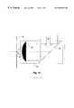
- a prior art scanner 50generates a moving spot of light 60 on a planar target surface 10 by focusing a collimated beam of light 20 through a focusing lens 40 . If the assembly is for reading information, reflected light from the constant intensity spot 60 is gathered by focusing lens 40 and returned toward a detector (not shown). To write information, the light-source is modulated. To cause the light spot 60 to move relative to the surface 10 , either the surface 10 is moved or the scanner 50 is moved.
- the optical pathcould have an acousto-optical beam deflector, a rotating prism-shaped mirror, or a lens driven galvanometrically or by piezoelectric positioners. Scanners also fall into two functional groups, raster and vector. Both types generally use the same types of beam deflection techniques.
- the performance parameters listed in Table 1assume different levels of importance depending on the optical scanning application. For raster scanning to cover extended surface areas, the emphasis is on speed, area resolution, and scan efficiency. Wide bandwidth is needed if the surface is to be color-scanned. For applications requiring vector scanning of precise paths at high resolution, the optical system typically uses a monochromatic, focused spot of light that is scanned at high speed with low wavefront distortion and low cross-axis error. Optical data storage has been a prime application of this type of optical scanning.
- optical data storage mediainformation is stored as an array of approximately wavelength-size dots (cells) in which some optical property has been set at one of two or more values to represent digital information.
- Commercial read/write headsscan the media with a diffraction-limited spot, typically produced by focusing a collimated laser beam with a fast objective lens system as shown in FIG. 1.
- a fast objective lensone with a high numerical aperture, achieves a small spot size by reducing Fraunhofer-type diffraction.
- the spotis scanned by moving an assembly of optical components (turning mirror, objective lens, position actuators) over the optical medium, either along a radius of a disc spinning under the spot or across the width of a tape moving past the head.
- the assemblymoves in one dimension along the direction of the collimated laser beam.
- the line of bit cellsmust be followed by the spot with sufficient precision to avoid missing any bit cells.
- the fine trackingis achieved by servo mechanisms moving the objective lens relative to the head assembly.
- An auto-focus servo systemis also necessary to maintain the diffraction limited spot size because the medium motion inevitably causes some change in the mean/medium separation with time. Proper focus adjustment is possible because the medium is flat and smooth. Such a surface reflects incident light in well-defined directions like a mirror. Light reflected from the medium is collected by focusing optics and sent back along the collimated beam path for detection.
- an alternating electric fieldgenerally perpendicular to the axis of the fiber.
- the fiberis coated with a metallic film.
- a chargeis stored on the film, especially near the tip, by forming a capacitance with a metallized plate oriented perpendicularly to the fiber axis (optically at least partly transparent). The stored charge makes the fiber responsive to the electric field.
- a drawback of this deviceis the limit on the speeds with which the fiber can be made to oscillate.
- the devicerequires a series of elements to move the fiber: an external field-generating structure, a DC voltage source to place charge on the fiber coating, and an AC source to generate the external field.
- Another drawback of this prior art mechanismis the inherent problem of stress fractures in the fiber optics. Bending the fiber repeatedly places serious demands on the materials. Problems can arise due to changes in optical properties, changes in the mechanical properties causing unpredictable variation in the alignment of the plane followed by the bending fiber, the amplitude of vibration, the natural frequency of vibrations, and structural failure.
- Still another limitationis imposed by the need to place a conductor between the fiber tip and the optical medium to form the capacitance. This places another optical element between the fiber tip and the scanned surface and makes it impossible to sweep the tip very close to the scanned surface as may be desired for certain optical configurations.
- This patent specificationdescribes a number of different devices to oscillate the end of an optical light guide or optical fiber.
- One embodimentemploys a piezo-electric bimorph connected to the free end of a device to which the free end of an optical fiber and a focusing lens are attached. Reflected light is directed back through the fiber to a beam splitter which directs the reflected light out of the bidirectional (outgoing/return) path at some point along the fiber remote from the source of light.
- the above embodimentuses a simpler prime mover, a piezo-electric bimorph.
- Friction between the motor and the fibercan cause changes in the optical properties of the fiber, and mechanical changes in the motor, the fiber, or the interface, that result in changes (which may be unpredictable) in the amplitude of oscillation or the resonant frequency of the motor-fiber combination (which might generate, or be susceptible to, undesired harmonics). Also, the process of assembly of such a combination of a motor and a fiber presents problems. Ideally, for high frequency operation, the device would be very small.
- a controller for a scanning headimages light emitted with a high numerical aperture from an output aperture using focusing optics with a one-to-one mapping of points in the output aperture plane onto points in the target plane.
- Lightis conducted to the output aperture by a light guide.
- the focus of the imaging opticsare a controlled by maximizing the received light.
- the light guidehas a directional coupler that taps received light and directs into a detector.
- the detector signalis applied to a control input through a low pass filter to obtain the focus control signal and applied to separate signal conditioning for data output.
- the controllercould internally register itself for the possible states of received light and respond accordingly. That is, the data stream is generated and supplied to the controller along with the total amount of light. The controller, if it determines that there is an amount of light that corresponds to neither kind of data (e.g., a one or a zero), it adjusts accordingly. In this way, the same device is used for both reading the data and controlling focus.
- the inventionprovides an optical scanning device.
- the devicehas a scanning head with a light output.
- a focusing elementimages light from the output onto a target surface.
- the focusing elementis effective to image a first amount of return light returned from the target surface back to the output when the focusing element is properly focused and a second amount of the return light, returned from the target surface back to the output, when the focusing element is improperly focused.
- a detector in a return path of the light, inside the scanning headgenerates an output responsive to the return light.
- a controlleris programmed to control a configuration of the focusing element responsive to the output such that the focusing element remains properly focused by maintaining the return light at the first amount.
- the scanning headincludes an optical fiber or guide with the output being an end of the optical fiber or guide.
- the light from the outputdiverges with a numerical aperture ratio of about 0.5.
- the focusing elementhas a 1:1 magnification.
- the scanning headincludes an optical fiber and the output is an end of the optical fiber.
- the scanning headincludes a directional coupler in series with the optical fiber or guide to divert light to the detector.
- the scanning headincludes multiple optical fibers or guides and the output is one of several outputs coinciding with respective ends of the optical fibers.
- the scanning headincludes directional couplers in series with the optical fibers to divert light to the detector or detectors.
- the inventionprovides an optical scanner with a scanning head having an array of optical fibers or guides. Each fiber or guide extends to the outside of the scanning head. This results in an array of light output apertures coinciding with ends of the optical fibers or guides.
- Light from the outputis imaged by a focusing element, with one-to-one mapping ratio, onto a target surface.
- the focusing elementis such that the amount of return light from the target surface back to the output, when the focusing element is properly focused, is at a maximum and less when out of focus.
- a detector in a return path of light in the scanning headgenerates an output responsive to the return light.
- a controlleris programmed to control a configuration of the focusing element responsively to the output such that the return light is maintained at the maximum.
- the light from the outputdiverges with a numerical aperture ratio of about 0.5.
- the magnification of the focusing elementis 1:1.
- the scanning headincludes a directional coupler in series with at least one of the optical fibers or guides to divert light to the detector.
- the scanning headhas a laser connected to direct light into the fiber or guide.
- the inventionprovides a method of controlling a focusing element of a scanning device. The method performs the following steps. Imaging, with a one-to-one mapping, an output of the scanning device onto a target surface to be read by the scanning device. Receiving light returned from an image of the output.
- the step of receivingincludes receiving light at an input aperture which is identical to an output aperture from which the output in the step of imaging is emitted.
- a light in single or multiple modes from a laser sourceis fed into one end of an optical fiber or waveguide designed so that this light diverges from the other end with a numerical aperture (NA) ratio determined by the fiber properties and tip configuration.
- NAnumerical aperture
- a simple optical system with matching NAis used to focus the light emitted from the fiber tip to produce the desired scanning spot size.
- Light reflected from the scanned surfacetravels back along the fiber, from which it is channeled to a sensor for signal detection.
- the property of this system in which it re-images and collects the returned light through the fiber when the spot is focused on the scanned surfacemeans that an autofocus system for the scanner will use the total light returned from a given surface area as a feedback parameter. When the light returned is maximized, the system is in focus.
- the scanningmay be achieved by moving the fiber and lens relative to the surface to be scanned. Other alternatives are moving the fiber tip relative to the optical axis and moving the lens relative to a fixed fiber tip.
- FIGS. 1A and 1Bare ray trace diagrams showing scanning devices according to the prior art.
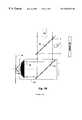
- FIG. 2Ais a ray trace diagram showing cantilever bimorph emitting light which is imaged onto a target surface and receiving return light from the target surface and tapped by a directional coupler and conveyed to a detector.
- FIG. 2Bis a section view of the bimorph of FIG. 2A showing, schematically, a laser source and a detector coupled to a light guide embedded therein by a directional coupler.
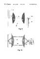
- FIG. 3illustrates spillover and vignetting effects for an off-axis source.
- FIG. 4is a diagram of a control scheme for maintaining focus of a lens system of the invention.
- FIG. 5illustrates the use of several light guides operating in parallel on adjoining areas of the same surface.
- FIG. 6is a ray trace diagram showing extreme positions of a cantilever mounted bimorph of FIG. 2 A.
- FIG. 7is a diagram illustrating a path followed by a tip of the bimorph of FIG. 2A as the bimorph bends.
- FIG. 8is a diagram illustrating a path followed by a tip of an alternate embodiment of a bimorph which is constructed or excited such that the tip follows a straight path.
- FIG. 9is a perspective diagram showing an alternative way of cantilever-mounting a bimorph to achieve constant axial position of the tip during bending.
- FIG. 10is a ray trace diagram showing a multiple channel scanning head according to an embodiment of the invention, where the imaging optics are fixed and the scanning head is oscillated by a MEMS motor to scan a region of a target surface.
- FIG. 11Ais a ray trace diagram showing a multiple channel scanning head according to an embodiment of the invention, where the imaging optics and scanning head are fixedly interconnected and oscillated as a unit by a MEMS motor to scan a region of a target surface.
- FIG. 11Bis a ray trace diagram showing a multiple channel scanning head according to an embodiment of the invention, where the imaging optics are oscillated as a unit by a MEMS motor to scan a region of a target surface.
- a scanning device 101employs a laser source 38 , which could be fundamental mode or multimode.
- Light from the laser source 38is fed into one end of a wave-guide, in the present embodiment, an optical fiber 33 .
- optical fiber 33may be embedded between two pieces of piezoelectric material 85 and 86 forming a bimorph/fiber element 80 .
- the tip 83 , of optical fiber 33is constructed to cause light emitted from it to diverge with a high numerical aperture ratio; of the order of 0.5.
- a fast lens system 46with lenses 42 and 44 , focuses light from the tip to a diffraction-limited spot 60 on a scanned surface 10 .
- Fiber tip 83is positioned so that it is substantially in the focal plane that is precisely imaged by lens system 46 onto surface 10 to form a light spot 60 .
- the effective size of the light sourceis the Gaussian beam waist of the fundamental mode within the fiber tip.
- the lens systemcould be made from one or more holographic elements (not shown).
- the highest resolution scanning applicationsrequire that a diffraction limited spot be used with fast optics.
- the NA required from the fiberdepends on the lens system magnification, and is 0.5 for the preferred case of 1:1 magnification.
- the fiber core diametermust be on the order of the laser light wavelength.
- near infrared and visible light applicationswhich have wavelengths in the range 0.5-1.0 ⁇ m, both lens and fiber technologies are well advanced.
- the axis of the cone of focused lightWhen the axis of the cone of focused light is perpendicular or nearly perpendicular to the scanned surface, most of the specularly reflected light is returned to the lens, i.e. it falls within a cone defined by the spot and the lens aperture. Any light reflected from the scanned surface within this cone is collected and re-imaged by the same lens system back into the fiber tip.
- the returned light signaltravels back along the fiber or waveguide, propagating in the direction opposite to the original light from the laser source. Before this return light reaches the source, it is diverted out of the path leading back to the source by a directional coupler 39 in the fiber/waveguide. From this coupler, the return light is channeled to a sensor 37 for signal detection.
- the one-to-one mapping property of imaging systemsconstrain the lens system to focus back into the fiber tip all light that originates from the spot 60 on the surface illuminated by that fiber tip.
- the acceptance aperture of the fiberacts as an aperture stop when collecting the return light. This fact minimizes noise and crosstalk in the returned light signal because light coming from other points on the scanned surface will not be re-imaged back onto the fiber tip.
- the fiber tip and scanning spotlie on the lens system axis as shown in FIGS. 2A and 2B, all specularly reflected light from the surface will be sent back into the fiber (minus losses from absorption and optical surface reflections).
- the arrangementwill also function when the tip source is displaced from the optical axis.
- some of the reflected lightwill be lost as “spillover” by vignetting effects.
- the amount of light lostdepends on whether the source is tilted (not shown), and can be minimized by a nearly telecentric optics design.
- lens design calculationshave shown that good system-performance (e.g., Strehl ratios of order 0.8 or higher) will be maintained.
- a control systemexploits the property by which return light is re-imaged and collected through the emitting fiber when the spot is focused on the scanned surface. If the system is in focus, the returned light forms a small image at the fiber tip, and most of the light enters the fiber tip and is detected. If the system is not in focus, the returned light is spread out over. a larger area, and a much smaller amount of light enters the fiber tip and is detected. Therefore, the system focuses can be controlled by maximizing the returned light as measured by the detector signal.
- a controller/driver 48receives a signal from the detector 37 and drives the focus-adjusting mechanism 48 a to maintain optimal focus.
- the focus adjusting mechanism(not shown in detail) may be any of a variety of mechanisms.
- a distance between lenses of a multiple-element systemcould be altered.
- the target surfacecould be moved axially relative to the entire scanning head.
- Just the output aperturecould be moved to adjust focus. If the focus is determined to be incorrect, the control system requires a signal that indicates which way to move.
- a signalcan be found by dithering (deliberately varying) the focus adjustment by a small amount and measuring changes in the return signal that are correlated with the dither variation.
- several light guidescan operate in parallel on adjoining areas of the same surface for faster data collection than a single scanner channel could achieve.
- multiple fiber sources 39 a, 39 b, and 39 ccan be imaged onto, scanned across, and re-imaged from a surface through a single lens system.
- the focus control signalmay be derived from one or more of the multiple data signal, or from separately placed and dedicated scanner channels (not shown but essentially as depicted for the dual-purpose channels of the embodiments pictured).
- the effective magnification of lens system 46is 1:1.
- a high numerical aperture at the output (scanned surface) end of the focusing opticsis desirable.
- At the input (laser) end of the focusing opticsit is desirable to minimize the off-axis displacement of the light source.
- a narrow sweep of the fiber/bimorph 80can translate into a large sweep of the spot 60 if the focusing optics have high magnification and high quality optics. This translates to fast optics and a high numerical aperture at the input of the bimorph.
- the focusing opticsare designed with as high numerical aperture as practical at the input and output ends and thus, with approximately 1:1 magnification.
- a numerical aperture of approximately 0.5is about as high as can be achieved.
- vibration of fiber 1is achieved by embedding it in a cantilever bimorph 80 designed to bend in response to an applied stimulus such as an electric field.
- the piezoelectric bimorph 80has two flat strips of piezoelectric material 85 and 86 joined lengthwise. Electrodes are attached in such a way as to induce elongation of one strip and contraction of the opposite strip when an electric field is applied. This action results in a bending motion of the unitary fiber/bimorph element 80 .
- the bending motionis reversed in direction, causing a vibrating motion when an AC voltage is applied continuously.
- a 4 ⁇ 4 matrixrelates the driving parameters to the response parameters. As bimorph 80 vibrates, the spot at the tip of fiber 1 is swept in an arc-shaped path.
- Focusing error caused by the arc-shaped sweep of the fiber tipmay be ameliorated not only by reducing the amplitude of the vibration of fiber/bimorph element 80 , but also by the use of certain non-conventional optics.
- non-conventional focusing opticsmay be shaped to image the locus of points defined by the curved path of sweep 88 of the fiber/bimorph element 80 tip 83 onto the plane 89 of the scanned surface 10 . That is, the optics are designed such that the tip 83 remains in focus at all cross-axis positions of tip 83 .
- still another way to ameliorate focusing error caused by the tendency of the fiber/bimorph element 80 to move axially as it bends away from the optical axisis to drive it in such a way that the tip 83 actually remains in a plane 78 .
- the first wayis to apply voltage to the piezoelectric elements such that the elements are extended as the tip moves away from the optical axis and contracted as the tip moves toward the axis. That is, the bimorph is stretched as it moves away from the axis and compressed as it moves toward the axis.
- the driving voltage differentialcauses the bending of the fiber/bimorph element and the net driving voltage produces elongation and contraction.
- still another way to ameliorate the focusing error caused by bendingis to position the fiber/bimorph element 80 such that the arc 88 of the sweep of tip 83 lies in a plane perpendicular to the optical axis.
- the spotsthen scan a curved path 76 on the scanned surface 10 . It is desirable for the surface to be written and read with the same arc-shaped sweep so that the data cells are aligned properly for both operations.
- the light guide arrayis an array of optical fibers.
- a scanning motion of multiple spots 60can be obtained with this arrangement.
- the multiple focused spots 60will scan over the surface 10 when the light guide array 180 is oscillated relative to the optical axis 90 of the lens system.
- the lens system 46is held fixed and the stage 181 is oscillated. In a nominal lens system with 1:1 magnification, the spots move along the surface 10 the same distance as the stage 181 .
- the focusing optics 46is oscillated.
- the focusing optics 46 and the light guide arrayare supported on a large stage 121 which is oscillated by a motor (not shown).
- lens system 46is supported on stage 125 that is oscillated relative to both the scanned surface 10 and the light guide array 180 .
- the lens systemis oscillated to cause a rotary motion since a purely lateral oscillation would not produce the same degree of oscillation in the focused spots 60 .
- the return light aperturedoes not have to be the same as the output aperture in order to achieve focusing control.
- the use of imaging opticsbring the specularly reflected return light back to the output aperture, and using a return aperture that is not the output aperture may be more complicated.
- the detected return light signalmay be sent through a low-pass filter to obtain an average signal to control focus.
- a sample-and-hold techniquecan be used to obtain a control signal to control reflectivity, and is correspondingly insensitive to data patterns that may be in the field of view.
- a headcould have separate exit apertures for reading and for writing, or have one set of apertures serving both functions.
Landscapes
- Physics & Mathematics (AREA)
- General Physics & Mathematics (AREA)
- Optics & Photonics (AREA)
- Engineering & Computer Science (AREA)
- Multimedia (AREA)
- Signal Processing (AREA)
- Mechanical Optical Scanning Systems (AREA)
- Facsimile Scanning Arrangements (AREA)
- Lens Barrels (AREA)
Abstract
Description
| TABLE 1 |
| Performance of Conventional |
| Beam Deflectors for Optical Scanning. |
| Galvano- | Acousto- | |||
| Polygonal | Driven | Hologons | Optic | |
| Parameter | Mirrors | Mirrors | (Transmission) | Deflectors |
| Wavefront | λ/8 at | λ/8 at | λ/6 at | λ/2 at |
| Distortion | 0.55 mm | 0.55 mm | 0.55 mm | 0.55 mm |
| area | 25,000 | 25,000 | 25,000 | 1,000 |
| resolution | (scan lens | (scan lens | (scan lens | (scan lens |
| (spot- | limited) | limited) | limited) | limited) |
| widths/ | ||||
| sec | ||||
| cross- | 1 0 | 1-2 | 10 | 0 |
| axis | arc sec | arc sec | arc sec | |
| error | (uncorrected) | (uncorrected) | ||
| 1 × 10⁸ | 2 × 10⁶ | 2 × 10⁷ | 2.8 × 10⁷ | |
| (spot | ||||
| widths/ | ||||
| sec) | ||||
| Bandwidth | 0.3-20 μm | 0.3-20 μm | monochromatic | monochromatic |
| scan | 80-100% | 65-90% | 90% | 60-80% |
| efficiency | ||||
Claims (21)
Priority Applications (4)
| Application Number | Priority Date | Filing Date | Title |
|---|---|---|---|
| US09/088,781US6584052B1 (en) | 1998-06-02 | 1998-06-02 | Method and apparatus for controlling the focus of a read/write head for an optical scanner |
| EP99927144AEP1084441A1 (en) | 1998-06-02 | 1999-06-02 | Method and apparatus for controlling the focus of a read/write head for an optical scanner |
| JP2000552539AJP2002517777A (en) | 1998-06-02 | 1999-06-02 | Method and apparatus for controlling the focus of a read / write head used in an optical scanner |
| PCT/US1999/012185WO1999063387A1 (en) | 1998-06-02 | 1999-06-02 | Method and apparatus for controlling the focus of a read/write head for an optical scanner |
Applications Claiming Priority (1)
| Application Number | Priority Date | Filing Date | Title |
|---|---|---|---|
| US09/088,781US6584052B1 (en) | 1998-06-02 | 1998-06-02 | Method and apparatus for controlling the focus of a read/write head for an optical scanner |
Publications (1)
| Publication Number | Publication Date |
|---|---|
| US6584052B1true US6584052B1 (en) | 2003-06-24 |
Family
ID=22213418
Family Applications (1)
| Application Number | Title | Priority Date | Filing Date |
|---|---|---|---|
| US09/088,781Expired - LifetimeUS6584052B1 (en) | 1998-06-02 | 1998-06-02 | Method and apparatus for controlling the focus of a read/write head for an optical scanner |
Country Status (4)
| Country | Link |
|---|---|
| US (1) | US6584052B1 (en) |
| EP (1) | EP1084441A1 (en) |
| JP (1) | JP2002517777A (en) |
| WO (1) | WO1999063387A1 (en) |
Cited By (23)
| Publication number | Priority date | Publication date | Assignee | Title |
|---|---|---|---|---|
| US20040022689A1 (en)* | 2002-08-02 | 2004-02-05 | Cybio Ag | Device for dispensing and observing the luminescence of individual specimens in multi-specimen arrangements |
| US6744459B2 (en)* | 2000-12-11 | 2004-06-01 | Minolta Co., Ltd. | Image forming apparatus using a single optical fiber to transmit electrical signals |
| US20040212553A1 (en)* | 2002-10-31 | 2004-10-28 | Microsoft Corporation | Pen projection display |
| US20060134535A1 (en)* | 2004-12-22 | 2006-06-22 | 3M Innovative Properties Company | Lensed fiber array for sub-micron optical lithography patterning |
| US7570813B2 (en) | 2004-01-16 | 2009-08-04 | Microsoft Corporation | Strokes localization by m-array decoding and fast image matching |
| US7580576B2 (en) | 2005-06-02 | 2009-08-25 | Microsoft Corporation | Stroke localization and binding to electronic document |
| US7583842B2 (en) | 2004-01-06 | 2009-09-01 | Microsoft Corporation | Enhanced approach of m-array decoding and error correction |
| US7599560B2 (en) | 2005-04-22 | 2009-10-06 | Microsoft Corporation | Embedded interaction code recognition |
| US7607076B2 (en) | 2005-02-18 | 2009-10-20 | Microsoft Corporation | Embedded interaction code document |
| US7619607B2 (en) | 2005-06-30 | 2009-11-17 | Microsoft Corporation | Embedding a pattern design onto a liquid crystal display |
| US7622182B2 (en) | 2005-08-17 | 2009-11-24 | Microsoft Corporation | Embedded interaction code enabled display |
| US7639885B2 (en) | 2002-10-31 | 2009-12-29 | Microsoft Corporation | Decoding and error correction in 2-D arrays |
| US7684618B2 (en) | 2002-10-31 | 2010-03-23 | Microsoft Corporation | Passive embedded interaction coding |
| US7729539B2 (en) | 2005-05-31 | 2010-06-01 | Microsoft Corporation | Fast error-correcting of embedded interaction codes |
| US7817816B2 (en) | 2005-08-17 | 2010-10-19 | Microsoft Corporation | Embedded interaction code enabled surface type identification |
| US7826074B1 (en) | 2005-02-25 | 2010-11-02 | Microsoft Corporation | Fast embedded interaction code printing with custom postscript commands |
| US7920753B2 (en) | 2005-05-25 | 2011-04-05 | Microsoft Corporation | Preprocessing for information pattern analysis |
| US8156153B2 (en) | 2005-04-22 | 2012-04-10 | Microsoft Corporation | Global metadata embedding and decoding |
| CN109844560A (en)* | 2016-10-17 | 2019-06-04 | 罗伯特·博世有限公司 | Optical element for laser radar system |
| US10698088B2 (en) | 2017-08-01 | 2020-06-30 | Waymo Llc | LIDAR receiver using a waveguide and an aperture |
| US10890650B2 (en) | 2017-09-05 | 2021-01-12 | Waymo Llc | LIDAR with co-aligned transmit and receive paths |
| US11041753B2 (en) | 2016-12-03 | 2021-06-22 | Waymo Llc | Light detection using an aperture |
| US11714171B2 (en) | 2016-12-01 | 2023-08-01 | Waymo Llc | Array of waveguide diffusers for light detection using an aperture and a given total internal reflection waveguide |
Families Citing this family (2)
| Publication number | Priority date | Publication date | Assignee | Title |
|---|---|---|---|---|
| WO2009115943A2 (en)* | 2008-03-18 | 2009-09-24 | Koninklijke Philips Electronics N.V. | Optical system |
| CN110376743B (en)* | 2014-01-31 | 2022-03-04 | 奇跃公司 | Multi-focus display system and method |
Citations (70)
| Publication number | Priority date | Publication date | Assignee | Title |
|---|---|---|---|---|
| US3112360A (en) | 1962-06-15 | 1963-11-26 | Winston Res Corp | Scanning with light-conducting rod |
| US3220013A (en) | 1963-10-21 | 1965-11-23 | Ibm | High speed electro-optic printer |
| US3892468A (en) | 1973-09-28 | 1975-07-01 | Bell Telephone Labor Inc | Optical scanner utilizing organ arrays of optical fibers |
| US3941927A (en) | 1974-11-11 | 1976-03-02 | Battelle Development Corporation | Optical fiber deflection device |
| US4058736A (en) | 1975-03-25 | 1977-11-15 | Eisai Co., Ltd. | Method and apparatus for inspecting extraneous solid substances contained in liquid |
| US4090206A (en) | 1976-07-15 | 1978-05-16 | Agfa-Gevaert Ag | Method and apparatus for producing successive lines of image points on a recording medium |
| US4135083A (en) | 1976-05-12 | 1979-01-16 | U.S. Philips Corporation | Optical scanning device |
| US4193091A (en) | 1977-12-12 | 1980-03-11 | U.S. Philips Corporation | Optical videodisc read unit with tracking and focussing wobblers |
| US4234788A (en) | 1979-04-06 | 1980-11-18 | General Dynamics Corporation, Pomona Division | Electrostatic fiber optic scanning device |
| US4283777A (en) | 1979-05-14 | 1981-08-11 | Xerox Corporation | Optical memory having a parallel read out |
| US4286145A (en) | 1980-02-20 | 1981-08-25 | General Dynamics, Pomona Division | Fiber optic bar code reader |
| US4337531A (en) | 1980-05-12 | 1982-06-29 | Northern Telecom Limited | Scanning head for an optical disc system |
| EP0092420A1 (en) | 1982-04-19 | 1983-10-26 | Xerox Corporation | Information storage systems |
| US4460989A (en) | 1981-06-22 | 1984-07-17 | Eli Soloman Jacobs | Apparatus for improving focus during playback of an optical data record |
| US4482986A (en) | 1981-01-30 | 1984-11-13 | Sony Corporation | Objective lens mount for optical disc player |
| US4500204A (en)* | 1981-04-21 | 1985-02-19 | Agency Of Industrial Science & Technology | Scanning-type lithographic and image-pickup device using optical fiber |
| US4507765A (en) | 1981-04-20 | 1985-03-26 | Junichi Suzuki | Optical track scanner |
| US4544259A (en) | 1983-07-13 | 1985-10-01 | Fuji Photo Film Co., Ltd. | Side printing apparatus |
| US4564268A (en) | 1981-05-29 | 1986-01-14 | Hitachi Ltd. | Optical system for semiconductor laser |
| US4566015A (en) | 1984-06-07 | 1986-01-21 | Polaroid Corporation | Image recording apparatus with adjustable mask |
| US4572949A (en) | 1982-04-14 | 1986-02-25 | The Board Of Trustees Of The Leland Stanford Junior University | Fiber optic sensor for detecting very small displacements of a surface |
| US4660094A (en) | 1983-03-08 | 1987-04-21 | Dainippon Screen Seizo Kabushiki Kaisha | Method for focus adjustment of a picture scanning and recording system |
| DE3717604A1 (en) | 1986-05-23 | 1987-11-26 | Olympus Optical Co | OPTICALLY WRITABLE AND / OR READABLE CARD |
| US4737946A (en) | 1984-09-03 | 1988-04-12 | Omron Tateisi Electronics Co. | Device for processing optical data with improved optical allignment means |
| WO1988003293A1 (en) | 1986-10-31 | 1988-05-05 | Drexler Technology Corporation | Transmissively read quad density otpical data system |
| US4744073A (en) | 1984-04-18 | 1988-05-10 | Sony Corporation | Recording/reproducing optical system utilizing semiconductor laser light source and anamorphic imaging element |
| US4755668A (en) | 1986-10-03 | 1988-07-05 | Optical Technologies, Inc. | Fiber optic interferometric thermometer with serially positioned fiber optic sensors |
| US4764738A (en) | 1987-03-26 | 1988-08-16 | D. L. Fried Associates, Inc. | Agile beam control of optical phased array |
| US4763973A (en) | 1985-02-27 | 1988-08-16 | Omron Tateisi Electronics Co. | Waveguide-type optical sensor |
| US4765703A (en) | 1985-08-05 | 1988-08-23 | Brother Kogyo Kabushiki Kaisha | Optical deflector |
| US4767210A (en) | 1983-02-24 | 1988-08-30 | British Telecommunications Plc | Optical fibre interferometer |
| US4771415A (en) | 1985-02-27 | 1988-09-13 | Brother Kogyo Kabushiki Kaisha | Optical data storage and readout apparatus and head, using optical fibers between stationary and movable units |
| US4815807A (en) | 1987-09-14 | 1989-03-28 | Mitsubishi Rayon Co., Ltd. | Collimator lens for optical fiber |
| US4858215A (en) | 1986-09-12 | 1989-08-15 | Sharp Kabushiki Kaisha | Integrated optical disc pickup that allows variations in the wavelength of the laser beam |
| US4991160A (en) | 1988-05-31 | 1991-02-05 | Nikon Precision Inc. | Integrated optical device for magneto-optical recording and reading head |
| US5001338A (en) | 1988-04-21 | 1991-03-19 | Societa' Cavi Pirelli S.P.A. | Body position sensor by phase comparison of modulated light waves transmitted through optical fiber |
| US5010346A (en) | 1989-10-27 | 1991-04-23 | The Boeing Company | Electro-optical analog-to-digital converter and method for digitizing an analog signal |
| US5031187A (en) | 1990-02-14 | 1991-07-09 | Bell Communications Research, Inc. | Planar array of vertical-cavity, surface-emitting lasers |
| US5070488A (en) | 1988-06-29 | 1991-12-03 | Atsuko Fukushima | Optical integrated circuit and optical apparatus |
| US5095472A (en) | 1989-06-02 | 1992-03-10 | Hitachi Cable Limited | Focusing error detecting system for optical head |
| US5109459A (en) | 1989-12-23 | 1992-04-28 | Dornier Luftfahrt Gmbh | Fiber optic scanner |
| US5121449A (en) | 1989-04-26 | 1992-06-09 | Hitachi, Ltd. | Information detecting system of scanning type |
| US5144616A (en) | 1989-03-14 | 1992-09-01 | Fuji Xerox Co., Ltd. | Laser diode and multibeam optical head using the laser diode |
| US5144604A (en) | 1989-07-26 | 1992-09-01 | Pioneer Electronic Corporation | Optical information reading apparatus having an optical integration type pickup |
| US5195152A (en) | 1991-11-04 | 1993-03-16 | Eastman Kodak Company | Multichannel optical recording apparatus employing laser diodes |
| US5220450A (en)* | 1991-06-26 | 1993-06-15 | Asahi Kogaku Kogyo K.K. | Scanning optical system capable of automatic focusing |
| US5278812A (en) | 1992-02-18 | 1994-01-11 | At&T Bell Laboratories | Tracking and focussing functions in optical disk apparatus |
| US5289454A (en) | 1991-12-19 | 1994-02-22 | Minnesota Mining And Manufacturing Company | Optical disc addressing devices a method of use thereof |
| US5293291A (en) | 1990-04-09 | 1994-03-08 | Nikon Corporation | Optical integrated device for magneto-optical reproducing head |
| US5317148A (en) | 1991-05-22 | 1994-05-31 | Loral Corporation | IR/ladar scanner |
| US5354985A (en) | 1993-06-03 | 1994-10-11 | Stanford University | Near field scanning optical and force microscope including cantilever and optical waveguide |
| US5390157A (en) | 1992-07-15 | 1995-02-14 | Eastman Kodak Company | Waveguide optical pick-up head using mach-zehnder interferometer wavefront sensor apparatus and method |
| EP0646908A1 (en) | 1993-10-04 | 1995-04-05 | Zen Research N.V. | Optical disk reader |
| US5414785A (en) | 1993-09-13 | 1995-05-09 | At&T Corp. | Optical data bus having collision detection capability |
| US5416881A (en) | 1992-08-20 | 1995-05-16 | Nippon Sheet Glass Co., Ltd. | Optical fiber and optical waveguide connecting device |
| US5422469A (en) | 1989-10-30 | 1995-06-06 | Symbol Technologies, Inc. | Fiber optic barcode readers using purely mechanical scanner oscillation |
| DE4401972A1 (en) | 1994-01-25 | 1995-07-27 | Dieter Prof Dr Roes | Optical surface scanning apparatus |
| US5444689A (en) | 1992-08-28 | 1995-08-22 | Nikon Corporation | Detection of phase and amplitude modulation information on optical medium with a waveguide |
| US5452382A (en) | 1992-09-07 | 1995-09-19 | Nikon Corporation | Optical waveguide device and optical microscope using the same |
| WO1995025971A2 (en) | 1994-03-24 | 1995-09-28 | Amfax Limited | Scanning apparatus and method |
| US5465243A (en) | 1992-04-24 | 1995-11-07 | E-Systems, Inc. | Optical recorder and reader of data on light sensitive media |
| US5483515A (en) | 1994-09-16 | 1996-01-09 | International Business Machines Corporation | Apparatus and method for cancelling cross-talk in signals from optical data storage systems |
| US5508990A (en) | 1990-06-12 | 1996-04-16 | Olympus Optical Co., Ltd. | Optical recording and reproducing apparatus using optical recording medium |
| US5564268A (en) | 1994-04-08 | 1996-10-15 | Ceeco Machinery Manufacturing Ltd. | Apparatus and method for the manufacture of uniform impedance communication cables for high frequency use |
| US5602863A (en) | 1993-07-20 | 1997-02-11 | Mitsubishi Denki Kabushiki Kaisha | Surface-emitting laser diode array and driving method thereof, photodetector, photodetector array, optical interconnection system, and multiwavelength optical communication system |
| US5661591A (en) | 1995-09-29 | 1997-08-26 | Texas Instruments Incorporated | Optical switch having an analog beam for steering light |
| US5727098A (en) | 1994-09-07 | 1998-03-10 | Jacobson; Joseph M. | Oscillating fiber optic display and imager |
| US5802222A (en) | 1995-02-07 | 1998-09-01 | Ldt Gmb&H Co. Laser-Display-Technologie Kg | Color image generation systems and applications |
| US5940564A (en) | 1997-08-05 | 1999-08-17 | Picolight, Inc. | Device for coupling a light source or receiver to an optical waveguide |
| US6084848A (en) | 1996-11-11 | 2000-07-04 | Kabushiki Kaisha Toshiba | Two-dimensional near field optical memory head |
Family Cites Families (1)
| Publication number | Priority date | Publication date | Assignee | Title |
|---|---|---|---|---|
| JPH05203445A (en)* | 1991-11-28 | 1993-08-10 | Brother Ind Ltd | Confocal focus position detector |
- 1998
- 1998-06-02USUS09/088,781patent/US6584052B1/ennot_activeExpired - Lifetime
- 1999
- 1999-06-02WOPCT/US1999/012185patent/WO1999063387A1/ennot_activeApplication Discontinuation
- 1999-06-02EPEP99927144Apatent/EP1084441A1/ennot_activeWithdrawn
- 1999-06-02JPJP2000552539Apatent/JP2002517777A/enactivePending
Patent Citations (72)
| Publication number | Priority date | Publication date | Assignee | Title |
|---|---|---|---|---|
| US3112360A (en) | 1962-06-15 | 1963-11-26 | Winston Res Corp | Scanning with light-conducting rod |
| US3220013A (en) | 1963-10-21 | 1965-11-23 | Ibm | High speed electro-optic printer |
| US3892468A (en) | 1973-09-28 | 1975-07-01 | Bell Telephone Labor Inc | Optical scanner utilizing organ arrays of optical fibers |
| US3941927A (en) | 1974-11-11 | 1976-03-02 | Battelle Development Corporation | Optical fiber deflection device |
| US4058736A (en) | 1975-03-25 | 1977-11-15 | Eisai Co., Ltd. | Method and apparatus for inspecting extraneous solid substances contained in liquid |
| US4135083A (en) | 1976-05-12 | 1979-01-16 | U.S. Philips Corporation | Optical scanning device |
| US4090206A (en) | 1976-07-15 | 1978-05-16 | Agfa-Gevaert Ag | Method and apparatus for producing successive lines of image points on a recording medium |
| US4193091A (en) | 1977-12-12 | 1980-03-11 | U.S. Philips Corporation | Optical videodisc read unit with tracking and focussing wobblers |
| US4234788A (en) | 1979-04-06 | 1980-11-18 | General Dynamics Corporation, Pomona Division | Electrostatic fiber optic scanning device |
| US4283777A (en) | 1979-05-14 | 1981-08-11 | Xerox Corporation | Optical memory having a parallel read out |
| US4286145A (en) | 1980-02-20 | 1981-08-25 | General Dynamics, Pomona Division | Fiber optic bar code reader |
| US4337531A (en) | 1980-05-12 | 1982-06-29 | Northern Telecom Limited | Scanning head for an optical disc system |
| US4482986A (en) | 1981-01-30 | 1984-11-13 | Sony Corporation | Objective lens mount for optical disc player |
| US4507765A (en) | 1981-04-20 | 1985-03-26 | Junichi Suzuki | Optical track scanner |
| US4500204A (en)* | 1981-04-21 | 1985-02-19 | Agency Of Industrial Science & Technology | Scanning-type lithographic and image-pickup device using optical fiber |
| US4564268A (en) | 1981-05-29 | 1986-01-14 | Hitachi Ltd. | Optical system for semiconductor laser |
| US4460989A (en) | 1981-06-22 | 1984-07-17 | Eli Soloman Jacobs | Apparatus for improving focus during playback of an optical data record |
| US4572949A (en) | 1982-04-14 | 1986-02-25 | The Board Of Trustees Of The Leland Stanford Junior University | Fiber optic sensor for detecting very small displacements of a surface |
| EP0092420A1 (en) | 1982-04-19 | 1983-10-26 | Xerox Corporation | Information storage systems |
| US4767210A (en) | 1983-02-24 | 1988-08-30 | British Telecommunications Plc | Optical fibre interferometer |
| US4660094A (en) | 1983-03-08 | 1987-04-21 | Dainippon Screen Seizo Kabushiki Kaisha | Method for focus adjustment of a picture scanning and recording system |
| US4544259A (en) | 1983-07-13 | 1985-10-01 | Fuji Photo Film Co., Ltd. | Side printing apparatus |
| US4744073A (en) | 1984-04-18 | 1988-05-10 | Sony Corporation | Recording/reproducing optical system utilizing semiconductor laser light source and anamorphic imaging element |
| US4566015A (en) | 1984-06-07 | 1986-01-21 | Polaroid Corporation | Image recording apparatus with adjustable mask |
| US5128915A (en) | 1984-09-03 | 1992-07-07 | Omron Tateisi Electronic Co. | Optical pickup device |
| US4737946A (en) | 1984-09-03 | 1988-04-12 | Omron Tateisi Electronics Co. | Device for processing optical data with improved optical allignment means |
| US4771415A (en) | 1985-02-27 | 1988-09-13 | Brother Kogyo Kabushiki Kaisha | Optical data storage and readout apparatus and head, using optical fibers between stationary and movable units |
| US4763973A (en) | 1985-02-27 | 1988-08-16 | Omron Tateisi Electronics Co. | Waveguide-type optical sensor |
| US4765703A (en) | 1985-08-05 | 1988-08-23 | Brother Kogyo Kabushiki Kaisha | Optical deflector |
| DE3717604A1 (en) | 1986-05-23 | 1987-11-26 | Olympus Optical Co | OPTICALLY WRITABLE AND / OR READABLE CARD |
| US4858215A (en) | 1986-09-12 | 1989-08-15 | Sharp Kabushiki Kaisha | Integrated optical disc pickup that allows variations in the wavelength of the laser beam |
| US4755668A (en) | 1986-10-03 | 1988-07-05 | Optical Technologies, Inc. | Fiber optic interferometric thermometer with serially positioned fiber optic sensors |
| WO1988003293A1 (en) | 1986-10-31 | 1988-05-05 | Drexler Technology Corporation | Transmissively read quad density otpical data system |
| US4764738A (en) | 1987-03-26 | 1988-08-16 | D. L. Fried Associates, Inc. | Agile beam control of optical phased array |
| US4815807A (en) | 1987-09-14 | 1989-03-28 | Mitsubishi Rayon Co., Ltd. | Collimator lens for optical fiber |
| US5001338A (en) | 1988-04-21 | 1991-03-19 | Societa' Cavi Pirelli S.P.A. | Body position sensor by phase comparison of modulated light waves transmitted through optical fiber |
| US4991160A (en) | 1988-05-31 | 1991-02-05 | Nikon Precision Inc. | Integrated optical device for magneto-optical recording and reading head |
| US5070488A (en) | 1988-06-29 | 1991-12-03 | Atsuko Fukushima | Optical integrated circuit and optical apparatus |
| US5144616A (en) | 1989-03-14 | 1992-09-01 | Fuji Xerox Co., Ltd. | Laser diode and multibeam optical head using the laser diode |
| US5121449A (en) | 1989-04-26 | 1992-06-09 | Hitachi, Ltd. | Information detecting system of scanning type |
| US5095472A (en) | 1989-06-02 | 1992-03-10 | Hitachi Cable Limited | Focusing error detecting system for optical head |
| US5144604A (en) | 1989-07-26 | 1992-09-01 | Pioneer Electronic Corporation | Optical information reading apparatus having an optical integration type pickup |
| US5010346A (en) | 1989-10-27 | 1991-04-23 | The Boeing Company | Electro-optical analog-to-digital converter and method for digitizing an analog signal |
| US5422469A (en) | 1989-10-30 | 1995-06-06 | Symbol Technologies, Inc. | Fiber optic barcode readers using purely mechanical scanner oscillation |
| US5109459A (en) | 1989-12-23 | 1992-04-28 | Dornier Luftfahrt Gmbh | Fiber optic scanner |
| US5031187A (en) | 1990-02-14 | 1991-07-09 | Bell Communications Research, Inc. | Planar array of vertical-cavity, surface-emitting lasers |
| US5293291A (en) | 1990-04-09 | 1994-03-08 | Nikon Corporation | Optical integrated device for magneto-optical reproducing head |
| US5508990A (en) | 1990-06-12 | 1996-04-16 | Olympus Optical Co., Ltd. | Optical recording and reproducing apparatus using optical recording medium |
| US5317148A (en) | 1991-05-22 | 1994-05-31 | Loral Corporation | IR/ladar scanner |
| US5220450A (en)* | 1991-06-26 | 1993-06-15 | Asahi Kogaku Kogyo K.K. | Scanning optical system capable of automatic focusing |
| US5195152A (en) | 1991-11-04 | 1993-03-16 | Eastman Kodak Company | Multichannel optical recording apparatus employing laser diodes |
| US5289454A (en) | 1991-12-19 | 1994-02-22 | Minnesota Mining And Manufacturing Company | Optical disc addressing devices a method of use thereof |
| EP0784314A1 (en) | 1991-12-19 | 1997-07-16 | Minnesota Mining And Manufacturing Company | Optical disc addressing devices |
| US5278812A (en) | 1992-02-18 | 1994-01-11 | At&T Bell Laboratories | Tracking and focussing functions in optical disk apparatus |
| US5465243A (en) | 1992-04-24 | 1995-11-07 | E-Systems, Inc. | Optical recorder and reader of data on light sensitive media |
| US5390157A (en) | 1992-07-15 | 1995-02-14 | Eastman Kodak Company | Waveguide optical pick-up head using mach-zehnder interferometer wavefront sensor apparatus and method |
| US5416881A (en) | 1992-08-20 | 1995-05-16 | Nippon Sheet Glass Co., Ltd. | Optical fiber and optical waveguide connecting device |
| US5444689A (en) | 1992-08-28 | 1995-08-22 | Nikon Corporation | Detection of phase and amplitude modulation information on optical medium with a waveguide |
| US5452382A (en) | 1992-09-07 | 1995-09-19 | Nikon Corporation | Optical waveguide device and optical microscope using the same |
| US5354985A (en) | 1993-06-03 | 1994-10-11 | Stanford University | Near field scanning optical and force microscope including cantilever and optical waveguide |
| US5602863A (en) | 1993-07-20 | 1997-02-11 | Mitsubishi Denki Kabushiki Kaisha | Surface-emitting laser diode array and driving method thereof, photodetector, photodetector array, optical interconnection system, and multiwavelength optical communication system |
| US5414785A (en) | 1993-09-13 | 1995-05-09 | At&T Corp. | Optical data bus having collision detection capability |
| EP0646908A1 (en) | 1993-10-04 | 1995-04-05 | Zen Research N.V. | Optical disk reader |
| DE4401972A1 (en) | 1994-01-25 | 1995-07-27 | Dieter Prof Dr Roes | Optical surface scanning apparatus |
| WO1995025971A2 (en) | 1994-03-24 | 1995-09-28 | Amfax Limited | Scanning apparatus and method |
| US5564268A (en) | 1994-04-08 | 1996-10-15 | Ceeco Machinery Manufacturing Ltd. | Apparatus and method for the manufacture of uniform impedance communication cables for high frequency use |
| US5727098A (en) | 1994-09-07 | 1998-03-10 | Jacobson; Joseph M. | Oscillating fiber optic display and imager |
| US5483515A (en) | 1994-09-16 | 1996-01-09 | International Business Machines Corporation | Apparatus and method for cancelling cross-talk in signals from optical data storage systems |
| US5802222A (en) | 1995-02-07 | 1998-09-01 | Ldt Gmb&H Co. Laser-Display-Technologie Kg | Color image generation systems and applications |
| US5661591A (en) | 1995-09-29 | 1997-08-26 | Texas Instruments Incorporated | Optical switch having an analog beam for steering light |
| US6084848A (en) | 1996-11-11 | 2000-07-04 | Kabushiki Kaisha Toshiba | Two-dimensional near field optical memory head |
| US5940564A (en) | 1997-08-05 | 1999-08-17 | Picolight, Inc. | Device for coupling a light source or receiver to an optical waveguide |
Non-Patent Citations (16)
| Title |
|---|
| "Miniature Micro-Optical Scanners", Optical Engineering, vol. 33, No. 11, Nov. 1, 1994, pp. 3616-3623 (Motamedi, M.E. et al). |
| Abstract of D.E. Brei and J. Blechschmidt, "Design and Static Modeling of a Semicircular Polymeric Piezoelectric Microactuator", (JMEMS, vol. 1, No. 3, p. 106). |
| Abstract of J.G. Smits and A. Ballato, "Dynamic Admittance Matrix of Piezoelectric Cantilever Bi-morphs", (JMEMS, vol. 3, No. 3, p. 105 et. seq.). |
| Abstract of J.W. Judy, R.S. Muller, and H.H. Zappe, "Magnetic Microactuation of Polysilicon Flexure Structures", (JMEMS, vol. 4, No. 4, p. 162). |
| Abstract of K. Minami, S. Kawamura, and M. Esashi, "Fabrication of Distributed Electrostatic Micro Actuator (DEMA)", (JMEMS, vol. 2, No. 3, p. 121 et. seq.). |
| Abstract of M. Ataka, A. Omodaka, N. Takeshima, and H. Fujita, "Fabrication and Operation of Polyimide Bimorph Actuators for a Ciliary Motion System", (JMEMS, vol. 2, No. 4, p. 146). |
| Abstract of Q. Meng, M. Mehregany, and R. L. Mullen, "Theoretical Modeling of Microfabricated Beams with Elastically Restrained Supports", (JMEMS, vol. 2, No. 3, p. 128 et. seq.). |
| Abstract of T.S. Low and W. Guo, "Modeling of a Three-Layer Piezoelectric Bimorph Beam with Hysteresis", (JMEMS, vol. 4, No. 4, p. 230). |
| Abstract of Yuji Uenishi, Hidenao Tanaka, and Hiro Ukita, "AlGaAs/GaAs micromachining for monolithic integration of optical and mechanical components", (Proc. SPIE vol. 2291, p. 82-91, Integrated Optics and Microstructures II, Massood Tabib-Azar; Dennis L. Polla; Ka-Kha Wong; Eds. Oct. 1994). |
| Multiple Channel Data Writing Device (Adam Thomas Drobot, Robert Courtney White, Newel Convers Wyeth, Albert Myron Green). Our Reference: 00479.02152, U.S. application Ser. No. 09/089,136, filed Jun. 2, 1998. |
| Multiple Channel Scanning Device Using Optoelectronic Switching (Adam Thomas Drobot, Robert Courtney White, Newel Convers Wyeth). Our Reference: 00479.02153, U.S. application Ser. No. 09/088,782, filed Jun. 2, 1998. |
| Multiple Channel Scanning Device using Oversampling and Image Processing to Increase Throughput (Adam Thomas Drobot, Robert Courtney White, Newel Convers Wyeth, Albert Myron Green, Edward Alan Phillips). Our Reference: 00479.02155, U.S. application Ser. No. 09/088,780, filed Jun. 2, 1998. |
| Multiple Parallel Source Scanning Device (Adam Thomas Drobot, Robert Courtney White, Newel Convers Wyeth). Our Reference: 00479.02151, U.S. application Ser. No. 09/089,137, filed Jun. 2, 1998. |
| Patent Abstracts of Japan, vol. 013, JP 01 152683 A, Jun. 15, 1989. |
| Patent Abstracts of Japan, vol. 017, No. 626 (P-1647), Nov. 18, 1993 and JP 05 203445 A, Aug. 10, 1993. |
| Scanning Device Using Fiber Optic Bimorph (Adam Thomas Drobot, Robert Courtney White). Our reference: 00479.02150, U.S. application Ser. No. 09/089,138, filed Jun. 2, 1998. |
Cited By (32)
| Publication number | Priority date | Publication date | Assignee | Title |
|---|---|---|---|---|
| US6744459B2 (en)* | 2000-12-11 | 2004-06-01 | Minolta Co., Ltd. | Image forming apparatus using a single optical fiber to transmit electrical signals |
| US7371347B2 (en)* | 2002-08-02 | 2008-05-13 | Cybio Ag | Device for dispensing and observing the luminescence of individual specimens in multi-specimen arrangements |
| US20040022689A1 (en)* | 2002-08-02 | 2004-02-05 | Cybio Ag | Device for dispensing and observing the luminescence of individual specimens in multi-specimen arrangements |
| US6964483B2 (en)* | 2002-10-31 | 2005-11-15 | Microsoft Corporation | Pen projection display |
| US7639885B2 (en) | 2002-10-31 | 2009-12-29 | Microsoft Corporation | Decoding and error correction in 2-D arrays |
| US20050073657A1 (en)* | 2002-10-31 | 2005-04-07 | Microsoft Corporation | Pen projection display |
| US20040212553A1 (en)* | 2002-10-31 | 2004-10-28 | Microsoft Corporation | Pen projection display |
| US7684618B2 (en) | 2002-10-31 | 2010-03-23 | Microsoft Corporation | Passive embedded interaction coding |
| US7583842B2 (en) | 2004-01-06 | 2009-09-01 | Microsoft Corporation | Enhanced approach of m-array decoding and error correction |
| US7570813B2 (en) | 2004-01-16 | 2009-08-04 | Microsoft Corporation | Strokes localization by m-array decoding and fast image matching |
| US20060134535A1 (en)* | 2004-12-22 | 2006-06-22 | 3M Innovative Properties Company | Lensed fiber array for sub-micron optical lithography patterning |
| US7607076B2 (en) | 2005-02-18 | 2009-10-20 | Microsoft Corporation | Embedded interaction code document |
| US7826074B1 (en) | 2005-02-25 | 2010-11-02 | Microsoft Corporation | Fast embedded interaction code printing with custom postscript commands |
| US7599560B2 (en) | 2005-04-22 | 2009-10-06 | Microsoft Corporation | Embedded interaction code recognition |
| US8156153B2 (en) | 2005-04-22 | 2012-04-10 | Microsoft Corporation | Global metadata embedding and decoding |
| US7920753B2 (en) | 2005-05-25 | 2011-04-05 | Microsoft Corporation | Preprocessing for information pattern analysis |
| US7729539B2 (en) | 2005-05-31 | 2010-06-01 | Microsoft Corporation | Fast error-correcting of embedded interaction codes |
| US7580576B2 (en) | 2005-06-02 | 2009-08-25 | Microsoft Corporation | Stroke localization and binding to electronic document |
| US7619607B2 (en) | 2005-06-30 | 2009-11-17 | Microsoft Corporation | Embedding a pattern design onto a liquid crystal display |
| US7622182B2 (en) | 2005-08-17 | 2009-11-24 | Microsoft Corporation | Embedded interaction code enabled display |
| US7817816B2 (en) | 2005-08-17 | 2010-10-19 | Microsoft Corporation | Embedded interaction code enabled surface type identification |
| US11255953B2 (en)* | 2016-10-17 | 2022-02-22 | Robert Bosch Gmbh | Optical element for a lidar system |
| CN109844560A (en)* | 2016-10-17 | 2019-06-04 | 罗伯特·博世有限公司 | Optical element for laser radar system |
| CN109844560B (en)* | 2016-10-17 | 2024-01-09 | 罗伯特·博世有限公司 | Optical element for a lidar system |
| US11714171B2 (en) | 2016-12-01 | 2023-08-01 | Waymo Llc | Array of waveguide diffusers for light detection using an aperture and a given total internal reflection waveguide |
| US12111422B2 (en) | 2016-12-01 | 2024-10-08 | Waymo Llc | Array of waveguide diffusers for light detection using an aperture |
| US11041753B2 (en) | 2016-12-03 | 2021-06-22 | Waymo Llc | Light detection using an aperture |
| US12078530B2 (en) | 2016-12-03 | 2024-09-03 | Waymo Llc | Light detection using an aperture |
| US11686823B2 (en) | 2017-08-01 | 2023-06-27 | Waymo Llc | LIDAR receiver using a waveguide and an aperture |
| US10698088B2 (en) | 2017-08-01 | 2020-06-30 | Waymo Llc | LIDAR receiver using a waveguide and an aperture |
| US10890650B2 (en) | 2017-09-05 | 2021-01-12 | Waymo Llc | LIDAR with co-aligned transmit and receive paths |
| US11802942B2 (en) | 2017-09-05 | 2023-10-31 | Waymo Llc | LIDAR with co-aligned transmit and receive paths |
Also Published As
| Publication number | Publication date |
|---|---|
| WO1999063387A9 (en) | 2000-03-09 |
| EP1084441A1 (en) | 2001-03-21 |
| WO1999063387A1 (en) | 1999-12-09 |
| JP2002517777A (en) | 2002-06-18 |
Similar Documents
| Publication | Publication Date | Title |
|---|---|---|
| US6584052B1 (en) | Method and apparatus for controlling the focus of a read/write head for an optical scanner | |
| US6559438B1 (en) | Multiple parallel source scanning device | |
| US6341118B1 (en) | Multiple channel scanning device using oversampling and image processing to increase throughput | |
| US6091067A (en) | Scanning device using fiber optic bimorph | |
| US5227910A (en) | High resolution laser beam scanner and method for operation thereof | |
| US4390235A (en) | Multibeam scanning apparatus provided with a function of changing magnification | |
| US5671077A (en) | Multi-beam light source device and optical scanning apparatus using the multi-beam source device | |
| US4299438A (en) | Scanning optical system having at least two reflecting surfaces and an afocal optical system | |
| JPH06318265A (en) | Laser scanning device for reading optical code | |
| JPH07501159A (en) | Active alignment system for coupling laser to fiber | |
| US6295171B1 (en) | Piezoelectric light beam deflector | |
| US6771421B2 (en) | Beam pattern contractor and focus element, method and apparatus | |
| US6294778B1 (en) | Method and apparatus for recording a flat field image | |
| US4852957A (en) | Optical system for flying spot scanning apparatus | |
| US6166756A (en) | Multiple channel data writing device | |
| WO2000019264A1 (en) | Scanning head lens assembly | |
| US6246658B1 (en) | Multiple channel scanning device using optoelectronic switching | |
| US4919502A (en) | Tilt error corrective scanning optical system | |
| US5438450A (en) | Optical scanning apparatus | |
| US6307799B1 (en) | Acousto optic data storage system on a stationary and high density data storage media | |
| JPH10221618A (en) | Multi-beam optics | |
| JPH0973056A (en) | Optical device using acousto-optic element | |
| JPH10206771A (en) | Raster output scanner | |
| JP3028633B2 (en) | Image recording device | |
| JPH0593879A (en) | Multiple light source unit |
Legal Events
| Date | Code | Title | Description |
|---|---|---|---|
| AS | Assignment | Owner name:SCIENCE APPLICATIONS INTERNATIONAL CORPORATION, CA Free format text:ASSIGNMENT OF ASSIGNORS INTEREST;ASSIGNORS:PHILLIPS, EDWARD ALAN;WYETH, NEWELL CONVERS;REEL/FRAME:009349/0643 Effective date:19980626 | |
| STCF | Information on status: patent grant | Free format text:PATENTED CASE | |
| FPAY | Fee payment | Year of fee payment:4 | |
| FPAY | Fee payment | Year of fee payment:8 | |
| AS | Assignment | Owner name:LEIDOS, INC., VIRGINIA Free format text:CHANGE OF NAME;ASSIGNOR:SCIENCE APPLICATIONS INTERNATIONAL CORPORATION;REEL/FRAME:032642/0107 Effective date:20130927 | |
| FPAY | Fee payment | Year of fee payment:12 | |
| AS | Assignment | Owner name:CITIBANK, N.A., DELAWARE Free format text:SECURITY INTEREST;ASSIGNOR:LEIDOS, INC.;REEL/FRAME:039809/0801 Effective date:20160816 Owner name:CITIBANK, N.A., DELAWARE Free format text:SECURITY INTEREST;ASSIGNOR:LEIDOS, INC.;REEL/FRAME:039818/0272 Effective date:20160816 | |
| AS | Assignment | Owner name:LEIDOS, INC., VIRGINIA Free format text:RELEASE BY SECURED PARTY;ASSIGNOR:CITIBANK, N.A., AS COLLATERAL AGENT;REEL/FRAME:051632/0819 Effective date:20200117 Owner name:LEIDOS, INC., VIRGINIA Free format text:RELEASE BY SECURED PARTY;ASSIGNOR:CITIBANK, N.A., AS COLLATERAL AGENT;REEL/FRAME:051632/0742 Effective date:20200117 |