US6583846B1 - Liquid crystal display device with spacer covered with an electrode - Google Patents
Liquid crystal display device with spacer covered with an electrodeDownload PDFInfo
- Publication number
- US6583846B1 US6583846B1US09/542,870US54287000AUS6583846B1US 6583846 B1US6583846 B1US 6583846B1US 54287000 AUS54287000 AUS 54287000AUS 6583846 B1US6583846 B1US 6583846B1
- Authority
- US
- United States
- Prior art keywords
- liquid crystal
- spacer
- display device
- crystal display
- transparent substrate
- Prior art date
- Legal status (The legal status is an assumption and is not a legal conclusion. Google has not performed a legal analysis and makes no representation as to the accuracy of the status listed.)
- Expired - Lifetime
Links
- 0*(c1ccccc1)c1ccccc1.CN.CNChemical compound*(c1ccccc1)c1ccccc1.CN.CN0.000description2
- QLPQZEMQNXBKTA-UHFFFAOYSA-NCC[Si](CC)(CCCCN)O[Si](CC)(CC)CCCCN.C[Si](C)(CCCN)O[Si](C)(C)CCCN.Cc1cc([Si](C)(C)O[Si](C)(C)c2ccc(N)c(C)c2)ccc1NChemical compoundCC[Si](CC)(CCCCN)O[Si](CC)(CC)CCCCN.C[Si](C)(CCCN)O[Si](C)(C)CCCN.Cc1cc([Si](C)(C)O[Si](C)(C)c2ccc(N)c(C)c2)ccc1NQLPQZEMQNXBKTA-UHFFFAOYSA-N0.000description1
- BYSLVGKEWPEEPI-UHFFFAOYSA-NNC(=O)c1cc(Oc2ccc(N)cc2)ccc1NChemical compoundNC(=O)c1cc(Oc2ccc(N)cc2)ccc1NBYSLVGKEWPEEPI-UHFFFAOYSA-N0.000description1
Images


Classifications
- G—PHYSICS
- G02—OPTICS
- G02F—OPTICAL DEVICES OR ARRANGEMENTS FOR THE CONTROL OF LIGHT BY MODIFICATION OF THE OPTICAL PROPERTIES OF THE MEDIA OF THE ELEMENTS INVOLVED THEREIN; NON-LINEAR OPTICS; FREQUENCY-CHANGING OF LIGHT; OPTICAL LOGIC ELEMENTS; OPTICAL ANALOGUE/DIGITAL CONVERTERS
- G02F1/00—Devices or arrangements for the control of the intensity, colour, phase, polarisation or direction of light arriving from an independent light source, e.g. switching, gating or modulating; Non-linear optics
- G02F1/01—Devices or arrangements for the control of the intensity, colour, phase, polarisation or direction of light arriving from an independent light source, e.g. switching, gating or modulating; Non-linear optics for the control of the intensity, phase, polarisation or colour
- G02F1/13—Devices or arrangements for the control of the intensity, colour, phase, polarisation or direction of light arriving from an independent light source, e.g. switching, gating or modulating; Non-linear optics for the control of the intensity, phase, polarisation or colour based on liquid crystals, e.g. single liquid crystal display cells
- G02F1/133—Constructional arrangements; Operation of liquid crystal cells; Circuit arrangements
- G02F1/1333—Constructional arrangements; Manufacturing methods
- G02F1/1337—Surface-induced orientation of the liquid crystal molecules, e.g. by alignment layers
- G02F1/133707—Structures for producing distorted electric fields, e.g. bumps, protrusions, recesses, slits in pixel electrodes
- A—HUMAN NECESSITIES
- A01—AGRICULTURE; FORESTRY; ANIMAL HUSBANDRY; HUNTING; TRAPPING; FISHING
- A01G—HORTICULTURE; CULTIVATION OF VEGETABLES, FLOWERS, RICE, FRUIT, VINES, HOPS OR SEAWEED; FORESTRY; WATERING
- A01G18/00—Cultivation of mushrooms
- A01G18/60—Cultivation rooms; Equipment therefor
- A01G18/64—Cultivation containers; Lids therefor
- A01G18/68—Cultivation bottles
- A—HUMAN NECESSITIES
- A01—AGRICULTURE; FORESTRY; ANIMAL HUSBANDRY; HUNTING; TRAPPING; FISHING
- A01G—HORTICULTURE; CULTIVATION OF VEGETABLES, FLOWERS, RICE, FRUIT, VINES, HOPS OR SEAWEED; FORESTRY; WATERING
- A01G18/00—Cultivation of mushrooms
- A01G18/60—Cultivation rooms; Equipment therefor
- A01G18/64—Cultivation containers; Lids therefor
- A01G18/65—Cultivation containers; Lids therefor characterised by the lids, e.g. lids with filters
- G—PHYSICS
- G02—OPTICS
- G02F—OPTICAL DEVICES OR ARRANGEMENTS FOR THE CONTROL OF LIGHT BY MODIFICATION OF THE OPTICAL PROPERTIES OF THE MEDIA OF THE ELEMENTS INVOLVED THEREIN; NON-LINEAR OPTICS; FREQUENCY-CHANGING OF LIGHT; OPTICAL LOGIC ELEMENTS; OPTICAL ANALOGUE/DIGITAL CONVERTERS
- G02F1/00—Devices or arrangements for the control of the intensity, colour, phase, polarisation or direction of light arriving from an independent light source, e.g. switching, gating or modulating; Non-linear optics
- G02F1/01—Devices or arrangements for the control of the intensity, colour, phase, polarisation or direction of light arriving from an independent light source, e.g. switching, gating or modulating; Non-linear optics for the control of the intensity, phase, polarisation or colour
- G02F1/13—Devices or arrangements for the control of the intensity, colour, phase, polarisation or direction of light arriving from an independent light source, e.g. switching, gating or modulating; Non-linear optics for the control of the intensity, phase, polarisation or colour based on liquid crystals, e.g. single liquid crystal display cells
- G02F1/133—Constructional arrangements; Operation of liquid crystal cells; Circuit arrangements
- G02F1/1333—Constructional arrangements; Manufacturing methods
- G02F1/1339—Gaskets; Spacers; Sealing of cells
- G02F1/13394—Gaskets; Spacers; Sealing of cells spacers regularly patterned on the cell subtrate, e.g. walls, pillars
- G—PHYSICS
- G02—OPTICS
- G02F—OPTICAL DEVICES OR ARRANGEMENTS FOR THE CONTROL OF LIGHT BY MODIFICATION OF THE OPTICAL PROPERTIES OF THE MEDIA OF THE ELEMENTS INVOLVED THEREIN; NON-LINEAR OPTICS; FREQUENCY-CHANGING OF LIGHT; OPTICAL LOGIC ELEMENTS; OPTICAL ANALOGUE/DIGITAL CONVERTERS
- G02F1/00—Devices or arrangements for the control of the intensity, colour, phase, polarisation or direction of light arriving from an independent light source, e.g. switching, gating or modulating; Non-linear optics
- G02F1/01—Devices or arrangements for the control of the intensity, colour, phase, polarisation or direction of light arriving from an independent light source, e.g. switching, gating or modulating; Non-linear optics for the control of the intensity, phase, polarisation or colour
- G02F1/13—Devices or arrangements for the control of the intensity, colour, phase, polarisation or direction of light arriving from an independent light source, e.g. switching, gating or modulating; Non-linear optics for the control of the intensity, phase, polarisation or colour based on liquid crystals, e.g. single liquid crystal display cells
- G02F1/133—Constructional arrangements; Operation of liquid crystal cells; Circuit arrangements
- G02F1/1333—Constructional arrangements; Manufacturing methods
- G02F1/1343—Electrodes
- G02F1/134309—Electrodes characterised by their geometrical arrangement
- G02F1/134363—Electrodes characterised by their geometrical arrangement for applying an electric field parallel to the substrate, i.e. in-plane switching [IPS]
- G—PHYSICS
- G02—OPTICS
- G02F—OPTICAL DEVICES OR ARRANGEMENTS FOR THE CONTROL OF LIGHT BY MODIFICATION OF THE OPTICAL PROPERTIES OF THE MEDIA OF THE ELEMENTS INVOLVED THEREIN; NON-LINEAR OPTICS; FREQUENCY-CHANGING OF LIGHT; OPTICAL LOGIC ELEMENTS; OPTICAL ANALOGUE/DIGITAL CONVERTERS
- G02F1/00—Devices or arrangements for the control of the intensity, colour, phase, polarisation or direction of light arriving from an independent light source, e.g. switching, gating or modulating; Non-linear optics
- G02F1/01—Devices or arrangements for the control of the intensity, colour, phase, polarisation or direction of light arriving from an independent light source, e.g. switching, gating or modulating; Non-linear optics for the control of the intensity, phase, polarisation or colour
- G02F1/13—Devices or arrangements for the control of the intensity, colour, phase, polarisation or direction of light arriving from an independent light source, e.g. switching, gating or modulating; Non-linear optics for the control of the intensity, phase, polarisation or colour based on liquid crystals, e.g. single liquid crystal display cells
- G02F1/133—Constructional arrangements; Operation of liquid crystal cells; Circuit arrangements
- G02F1/136—Liquid crystal cells structurally associated with a semi-conducting layer or substrate, e.g. cells forming part of an integrated circuit
- G02F1/1362—Active matrix addressed cells
- G02F1/136213—Storage capacitors associated with the pixel electrode
Definitions
- the present inventionrelates to a liquid crystal display device, and particularly to a liquid crystal display device provided with spacers sandwiched between a pair of opposing substrates with a liquid crystal layer interposed therebetween.
- Placement of spacers between a pair of opposing substrates with a liquid crystal layer therebetweencan establish a uniform thickness of the liquid crystal layer and thereby prevent occurrence of non-uniformity in a displayed image.
- Beadsfor example, are used as spacers. Initially beads are dispersed on a surface of one of a pair of substrates facing toward a liquid crystal layer, and then the other of the pair of substrates is overlapped over the one of the pair. But the surfaces of the substrates are uneven, some spacers are positioned in indented portions in the surfaces of the substrates, others are positioned in raised portions in the surfaces in the substrates, and consequently, the desired spacing between the pair of substrates are not sometimes obtained.
- spacerswhich are fixed at predetermined positions on a surface of one of a pair of substrates facing toward a liquid crystal layer before the other of the pair of substrates is overlapped over the one of the pair.
- the spacersare formed only on indented portions in the uneven substrate, for example, and consequently, the desired spacing between the pair of substrates is obtained.
- the spacers of the above-explained type having the spacers fixed on a substratehave the above advantage and can also improve the display quality further by optimizing the arrangement of the spacers.
- the present inventionhas been made in this situation, and the purpose of the present invention is to provide a liquid crystal display device having the quality of a displayed image improved.
- a liquid crystal display devicecomprising: a pair of opposing substrates, at least one of said pair of opposing substrates being transparent, a liquid crystal film sandwiched between said pair of opposing substrates, a plurality of electrodes of a first kind disposed on an inner surface of one of said pair of opposing substrates for defining a plurality of pixels, at least one electrode of a second kind disposed on an inner surface of one of (1) said one of said pair of opposing substrates so as to be adjacent to, but spaced from said plurality of electrodes of said first kind and (2) another of said pair of opposing substrates so as to face said plurality of electrodes of said first kind, and at least one spacer disposed approximately at a center of at least one of said plurality of pixels for establishing a spacing between said pair of opposing substrates, said at least one spacer being fixed to one of said pair of opposing substrates and covered with one of (1) a corresponding one of said plurality of
- a liquid crystal display devicecomprising: a pair of opposing substrates, at least one of said pair of opposing substrates being transparent, a liquid crystal film sandwiched between said pair of opposing substrates, a plurality of electrodes of a first kind disposed on an inner surface of one of said pair of opposing substrates for defining a plurality of pixels, at least one electrode of a second kind disposed on an inner surface of one of (1) said one of said pair of opposing substrates so as to be adjacent to, but spaced from said plurality of electrodes of said first kind and (2) another of said pair of opposing substrates so as to face said plurality of electrodes of said first kind, and at least one spacer disposed approximately at a center of at least one of said plurality of pixels for establishing a spacing between said pair of opposing substrates, said at least one spacer being fixed to one of said pair of opposing substrates and covered with one of (1) a corresponding one of said plurality of
- a liquid crystal display devicecomprising: a pair of opposing substrates, at least one of said pair of opposing substrates being transparent, a liquid crystal film sandwiched between said pair of opposing substrates, a plurality of electrodes of a first kind disposed on an inner surface of one of said pair of opposing substrates for defining a plurality of pixels, a plurality of wiring lines of a first kind coupled to said plurality of electrodes of said first kind, at least one electrode of a second kind disposed on an inner surface of one of (1) said one of said pair of opposing substrates so as to be adjacent to, but spaced from said plurality of electrodes of said first kind and (2) another of said pair of opposing substrates so as to face said plurality of electrodes of said first kind, at least one wiring line of a second kind coupled to said at least one electrode of said second kind, and at least one spacer disposed approximately at a center of at least one of said plurality of pixels for
- the so-called multi-domain effectis that obtained by subdividing one pixel into a plurality of regions provided with different angular dependence of the electro-optic characteristics to reduce the angular dependence of the one pixel as a whole and thereby to eliminate or reduce the above-mentioned reversal in transmitted light intensity.
- FIG. 1Ais a plan view of a pixel in a liquid crystal display device in accordance with an embodiment of the present invention
- FIG. 1Bis a cross-sectional view of the pixel taken along line b—b of FIG. 1A;
- FIG. 2is an illustration of an arrangement of main chains in an example of liquid crystal orientation film used in a liquid crystal display device of the present invention before being subjected to a rubbing treatment;
- FIG. 3is an illustration of an arrangement of main chains in the example of the liquid crystal orientation film of FIG. 2 after having been subjected to a rubbing treatment;
- FIG. 4Ais a plan view of a pixel in a liquid crystal display device in accordance with still another embodiment of the present invention
- FIG. 4Bis a cross-sectional view of the pixel taken along line b—b of FIG. 4A;
- FIG. 5is a plan view of a pixel in a liquid crystal display device in accordance with still another embodiment of the present invention.
- FIG. 6Ais a plan view of an intersection of a gate line and a drain line with an insulating film interposed therebetween for explaining a problem with the intersection
- FIG. 6Bis a cross-sectional view of the intersection taken along line b—b of FIG. 6A;
- FIG. 7is a plan view of a pixel in a liquid crystal display device in accordance with still another embodiment of the present invention.
- FIG. 8Ais a plan view of a thin film transistor for explaining a problem with the thin film transistor
- FIG. 8Bis a cross-sectional view of the thin film transistor taken along line b—b of FIG. 8A;
- FIG. 9is a plan view of a pixel in a liquid crystal display device in accordance with still another embodiment of the present invention.
- FIG. 10is a plan view of a pixel in a liquid crystal display device in accordance with still another embodiment of the present invention.
- FIG. 11Ais a plan view of a pixel in a liquid crystal display device in accordance with still another embodiment of the present invention, and FIG. 11B is a cross-sectional view of the pixel taken along line b—b of FIG. 11A;
- FIG. 12Ais a plan view of a pixel in a liquid crystal display device in accordance with still another embodiment of the present invention, and FIG. 12B is a cross-sectional view of the pixel taken along line b—b of FIG. 12A;
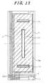
- FIG. 13Ais a plan view of a pixel in a liquid crystal display device in accordance with still another embodiment of the present invention, and FIG. 13B is a cross-sectional view of the pixel taken along line b—b of FIG. 13A;
- FIG. 14Ais a plan view of a pixel in a liquid crystal display device in accordance with still another embodiment of the present invention, and FIG. 14B is a cross-sectional view of the pixel taken along line b—b of FIG. 14A;
- FIG. 15is a plan view of a pixel in a liquid crystal display device in accordance with still another embodiment of the present invention.
- FIG. 16is a plan view of a pixel in a liquid crystal display device in accordance with still another embodiment of the present invention.
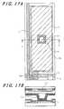
- FIG. 17Ais a plan view of a pixel in a liquid crystal display device in accordance with still another embodiment of the present invention, and FIG. 17B is a cross-sectional view of the pixel taken along line b—b of FIG. 17A;
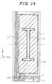
- FIG. 18Ais a plan view of a pixel in a liquid crystal display device in accordance with still another embodiment of the present invention, and FIG. 18B is a cross-sectional view of the pixel taken along line b—b of FIG. 18A;
- FIG. 19is a plan view of an example of a spacer used in a liquid crystal display device of the present invention.
- FIG. 20is a plan view of the spacer of FIG. 19 for explaining an advantage provided by the spacer;
- FIG. 21is a fragmentary perspective view of a liquid crystal display device in accordance with still another embodiment of the present invention.
- FIG. 22is a plan view of a liquid crystal display device in accordance with still another embodiment of the present invention.
- FIG. 23is a perspective view of another example of a spacer used in a liquid crystal display device of the present invention.
- FIG. 24is a perspective view of still another example of a spacer used in a liquid crystal display device of the present invention.
- FIG. 25is a cross-sectional view of a liquid crystal display device in accordance with still another embodiment of the present invention.
- FIG. 26is a cross-sectional view of a liquid crystal display device in accordance with still another embodiment of the present invention.
- FIG. 27is a cross-sectional view of a liquid crystal display device in accordance with still another embodiment of the present invention.
- FIG. 28Ais a plan view of a liquid crystal display device in accordance with still another embodiment of the present invention
- FIG. 28Bis a plan view of a liquid crystal display device in accordance with still another embodiment of the present invention
- FIG. 29is a cross-sectional view of a liquid crystal display device in accordance with still another embodiment of the present invention.
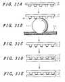
- FIGS. 30A to 30 Eillustrate the steps of an exemplary method of manufacturing the liquid crystal display device of FIG. 29;
- FIGS. 31A to 31 Eillustrate the steps of another exemplary method of manufacturing the liquid crystal display device of FIG. 29;
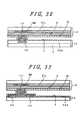
- FIG. 32is a cross-sectional view of a liquid crystal display device in accordance with still another embodiment of the present invention.
- FIG. 33is a cross-sectional view of a liquid crystal display device in accordance with still another embodiment of the present invention.
- FIGS. 1A and 1Billustrate a configuration of an embodiment of the liquid crystal display device according to the present invention.
- FIG. 1Ais a plan view of one of a plurality of pixels in a liquid crystal display device of the so-called horizontal electric field type
- FIG. 1Bis a cross-sectional view of the pixel of FIG. 1A taken along line b—b of FIG. 1 A.
- the pixels as illustrated in FIGS. 1A and 1Bare arranged in the form of a matrix to constitute a display area.
- the transmission of light at each pixelis controlled by a horizontal electric field applied in parallel with a layer of liquid crystal material sandwiched between opposing transparent electrodes formed on the inner surfaces of the opposing transparent substrates.
- Each pixelis formed by two electrodes formed on one of a pair of opposing substrates.
- a scanning signal line (a gate line) 2extends in the x direction in FIG. 1 A and is made of a chromium film, for example. As shown in FIG. 1A, the gate line 2 is disposed below the pixel area, for example, to maximize the effective area of the pixel.
- the gate line 2is supplied with a gate signal from a circuit external to the display area so as to drive a thin film transistor TFT described subsequently.
- a counter-voltage signal line 4extends in the x direction in FIG. 1 A and is made of the same material as the gate line 2 , for example.
- a plurality (three, for example) of counter electrodes 4 A made integrally with the counter-voltage signal line 4extend in a direction perpendicular to the counter-voltage signal line 4 , i. e. ⁇ y direction, for example.
- the counter electrodes 4 Aare supplied with a signal serving as a reference voltage for a video signal supplied to a pixel electrode 5 subsequently described via the counter-voltage signal line 4 , so as to generate an electric field of the strength corresponding to the video signal between the pixel electrode 5 and the counter electrodes 4 A.
- the generated electric fieldcontains a component parallel with the major surface of the transparent substrate 1 and this component controls light transmission through the liquid crystal layer.
- This type of the liquid crystal display deviceuses a component of an electric field in parallel with the major surface of the transparent substrate 1 , and it is this reason that this type is called the horizontal electric field type.
- the counter-voltage signal line 4is supplied with a reference voltage from a circuit external to the display area.
- the insulating film INSserves as a gate insulating film in an area formed with a thin film transistor TFT described subsequently, serves as an interlayer insulating film between the gate lines 2 and the counter-voltage signal lines 4 in an area formed with video signal lines (drain lines) 3 described subsequently, and serves as a dielectric film in an area formed with a capacitor Cadd described subsequently.
- a drain electrode 3 A and a source electrode 5 Aare disposed on the top of the semiconductor layer 6 to form the thin film transistor TFT of the so-called inverted staggered structure by using a portion of the gate line 2 as a gate electrode.
- the drain electrode 3 A and the source electrode 5 Aare formed on the semiconductor layer 6 together with the pixel electrode 5 simultaneously with formation of the drain line 3 , for example.
- the drain line 3is formed to extend in the y direction, and the drain electrode 3 A formed integrally with the drain line 3 is disposed on the semiconductor layer 6 .
- the drain line 3is disposed to the left of the pixel area, for example, to maximize the effective pixel area, as shown in FIG. 1 A.
- the source electrode 5 Ais formed simultaneously with the drain line 3 and integrally with the pixel electrode 5 .
- the pixel electrode 5is formed to extend between the two adjacent counter electrodes 4 A in the y direction in FIG. 1 A.
- the two counter electrodes 4 Aare disposed on opposite sides of the pixel electrode 5 , and are spaced approximately equal distances from the pixel electrode 5 so as to generate electric fields between the pixel electrode 5 and the counter electrodes 4 A.
- a portion of the pixel electrode 5 facing the counter-voltage signal line 4is configured so as to increase its area and to form a capacitor Cadd by using the insulating film INS as a dielectric.
- the capacitor Caddserves to store a video signal supplied to the pixel electrode 5 , for example, for a comparatively longer time.
- the thin film transistor TFTis turned on by a scanning signal supplied from the gate line 2 , a video signal from the drain line 3 is supplied to the pixel electrode 5 via the thin film transistor TFT, and then after the thin film transistor TFT is turned off, the video signal having been supplied to the pixel electrode 5 is stored in the capacitor Cadd.
- An orientation film 7is formed on the protective film PAS so as to determine the direction of initial orientation of the liquid crystal molecules.
- the thus processed transparent substrateis called the TFT substrate 1 A.
- a liquid crystal panelis completed by superposing the TFT substrate 1 A on a transparent substrate called the filter substrate 1 B with a liquid crystal layer interposed therebetween such that the orientation film 7 of the TFT substrate 1 A is in contact with the liquid crystal layer.
- a black matrix BMis formed on the surface of the filter substrate 1 B on the liquid crystal-layer side thereof for defining the contour of the pixel area as indicated in FIG. 1A, a color filter FIL is formed in the opening (a central portion of the pixel area excluding its periphery) in the black matrix BM, and a planarizing film 8 is formed on the surface of the transparent substrate 1 B including the black matrix BM and the color filter FIL.
- a spacer 10is formed on the planarizing film 8 such that the spacer 10 is superposed on the approximately central portion of the area forming the capacitor Cadd.
- the spacer 10is formed by coating synthetic resin, for example, on the planarizing film 8 and then by patterning the synthetic resin layer by a photolithography technique (and also by selective etching, if necessary).
- the height of the spacer 10controls the spacing between the TFT substrate 1 A and the filter substrate 1 B sandwiching the liquid crystal layer.
- the spacer 10is superposed on the capacitor Cadd is that the width of the counter-voltage signal line 4 lying below it is made comparatively wider than that of the other signal lines, and consequently, an area of the orientation film 11 suffering from orientation defects caused by the spacer 10 explained later is prevented from passing light through the area by the counter-voltage signal line 4 .
- Another reasonis that the spacer 10 is positioned at an approximately center of the pixel area surrounded by the black matrix BM, thereby it becomes easier to control the thickness of the liquid crystal layer (the spacing between the two substrates) in the pixel.
- the orientation 11is formed on the surface of the filter substrate 1 B including the spacers 10 as shown in FIG. 1 B.
- the orientation film 11is fabricated by coating synthetic resin, for example, on the planarizing film 8 and then rubbing the synthetic resin film. It is inevitable that orientation defects in the orientation film 11 is caused around the vicinity of the spacer 10 by rubbing the synthetic resin film. But the area suffering from the orientation defects is prevented sufficiently from passing light through the area by the light-blocking counter-voltage signal line 4 as explained above.
- the spacer 10is formed to be superposed on the capacitor Cadd, but the present invention is not limited to this arrangement.
- the spacer 10may be formed to be superposed on a portion of the counter-voltage signal line 4 displaced from the capacitor Cadd. In this case, the spacer 10 may be superposed on a different signal line, for example, which traverses the pixel area.
- the spacer 10is formed on the filter substrate 1 B, but the spacer 10 may be formed on the TFT substrate 1 A. This arrangement provides an advantage that the spacer 10 is positioned accurately with respect to the counter-voltage signal line 4 .
- This embodimentexplains the concrete configurations of the orientation films 7 , 11 in the liquid crystal display device of Embodiment 1.
- the rubbing directions of the orientation films 7 , 11correspond to the directions of the initial orientations of liquid crystal molecules, and the orientation films 7 and 11 of the TFT substrate 1 A and the filter substrate 1 B, respectively, are rubbed in the same direction, in other words, the directions of the initial orientations of the orientation films 7 and 11 are parallel with each other.
- the orientation film 11 formed on the top of the spacer 10contacts the orientation film 7 formed on the filter substrate 1 A, and it was confirmed that adhesion at the contact area is increased.
- main chains of the materialare randomly arranged as illustrated in FIG. 2, for example, but in the synthetic resin film rubbed in the direction as described, main chains of the material are arranged in one direction and consequently, the orientation films 7 , 11 are bonded together firmly by the intermolecular force.
- the orientation filmis composed of a polyimide resin film of 50 nm in thickness and made from 2,2-bis[4-(p-aminophenoxy)phenylpropane] and pyromellitic dianhydride, for example.
- amines to be copolymerized with tetracarboxylic acid dianhydrideare as follows:
- Xdenotes a direct coupling, —O—, —CH 2 —, —SO 2 —, —Co—, —CO 2 —, or —CONH—, or compounds having a structure represented by one of the formulas below,
- Xdenotes a direct coupling, a compound of bis(aminophenoxy)diphenyl, for example.
- the exemplary diamines to be copolymerized with tetracarboxylic acid dianhydride, but not containing halogen radicalsare as follows:
- acid compounds having a long-chain alkylene radical and other copolymerizable compoundsare as follows: octylsuccinic dianhydride, dodecylsuccinic dianhydride, octylmalonic dianhydride, decamethylenebistribenzenehexacarboxylic dianhydride, decamethylenebistrimethylenebistribenzenehexacarboxylic dianhydride, 2,2-bis[4-(3, 4-dicarboxyphenoxy)phenyl]octyltetracarboxylic dianhydride, 2,2-bis[4-(3, 4-dicarboxybenzoyloxy)phenyl]tridecanetetracarboxylic dianhydride, 2,2-bis[4-(3,4-dicarboxyphenoxy)phenyl]tridecanetetracarboxylic dianhydride, stearic acid, stearylchloride, pyromellitic dianhydride, methylpyrom
- FIGS. 4A and 4Billustrate a configuration of another embodiment of the liquid crystal display device according to the present invention.
- FIG. 4Ais a plan view of one of a plurality of pixels in a liquid crystal display device of the so-called horizontal electric field type
- FIG. 4Bis a cross-sectional view of the pixel of FIG. 1A taken along line b—b of FIG. 4 A.
- the pixels as illustrated in FIGS. 4A and 4Bare arranged in the form of a matrix to constitute a display area.
- FIGS. 4A and 4Bis similar to the embodiment illustrated in FIGS. 1A and 1B, except that a light-blocking film 15 made of the same material as the black matrix BM and having an area larger than the spacer 10 is formed below and centered on the spacer 10 on the filter substrate 1 B.
- the object of this embodimentis to ensure the masking effect of the light-blocking film 15 by enlarging the masking area around the spacer 10 without producing adverse effects on the aperture ratio of the pixel.
- the light-blocking film 15can be formed simultaneously with the formation of the black matrix BM, and consequently, it is advantageous that no additional manufacturing is needed.
- the light-blocking film 15does not need to be formed of the same material as the black matrix BM.
- FIG. 5illustrates a configuration of another embodiment of the liquid crystal display device according to the present invention, and is a plan view of one of a plurality of pixels in a liquid crystal display device of the so-called horizontal electric field type corresponding to FIG. 1 A.
- FIG. 5is similar to the embodiment illustrated in FIGS. 1A and 1B, except that the spacer 10 is located at the intersection of the gate line 2 and the drain line 3 to cover the intersection.
- the reason why the spacer 10 is located at the intersection of the gate line 2 and the drain line 3is that the liquid crystal material is prevented from being present at the intersection so that metal components of the drain line 3 is prevented from being dissolved into the liquid crystal material due to electrochemical reaction with the liquid crystal material serving as an electrolyte.
- FIG. 6Ais a plan view of the intersection of the gate line 2 and the drain line 3 with the insulating film INS interposed therebetween
- FIG. 6Bis a cross-sectional view of the intersection taken along line b—b of FIG. 6 A.
- the growth of the protective film PAS from over the top of the intersectioninterferes with that of the protective film PAS on the insulating film INS at the intersection of the edges of long sides of the gate line 2 and the drain line 3 (i.e. at corners of the intersection), the protective film PAS cannot cover the intersection sufficiently, and consequently, the liquid crystal material sometimes penetrates into the intersection and contacts the drain line 3 on the insulating film INS. In such a case, it is inevitable that metal components of the drain line 3 dissolve into the liquid crystal material by the so-called galvanic corrosion.
- the spacer 10is disposed so as to cover the intersection of the gate line 2 and the drain line 3 and prevent penetration of the liquid crystal material into the intersection in this embodiment.
- FIG. 7illustrates a configuration of another embodiment of the liquid crystal display device according to the present invention, and is a plan view of one of a plurality of pixels in a liquid crystal display device of the so-called horizontal electric field type corresponding to FIG. 1 A.
- FIG. 7is similar to the embodiment illustrated in FIG. 5, except that the spacer 10 is located at an area where the thin film transistor TFT is formed to cover the thin film transistor TFT.
- the spacer 10covers the thin film transistor TFT such that at least corners of the drain electrode 3 A or the source electrode 5 A of the thin film transistor TFT.
- FIG. 8Ais a plan view of the thin film transistor TFT
- FIG. 8Bis a cross-sectional view of the thin film transistor TFT taken along line b—b of FIG. 8 A.
- the galvanic corrosion of the drain electrode 3 A or the source electrode 5 Achanges the width of the channel of the thin film transistor TFT, and consequently, it is very advantageous that the galvanic corrosion can be prevented.
- the semiconductor layer 6 forming the thin film transistor TFTcan be considered as a conductive layer, and it may have a problem with the gate line 2 similar to the problem explained in Embodiment 4, and consequently, it is very effective to dispose the spacer 10 to cover the area where the thin film transistor TFT is formed.
- FIG. 9illustrates a configuration of another embodiment of the liquid crystal display device according to the present invention, and is a plan view of one of a plurality of pixels in a liquid crystal display device of the so-called horizontal electric field type corresponding to FIG. 1 A.
- FIG. 9is similar to the embodiment illustrated in FIG. 5, except that the spacer 10 is located at the intersection of the counter-voltage signal line 4 and the drain line 3 to cover the intersection.
- the liquid crystal display device having this configurationprevents the galvanic corrosion of the drain line 3 for the reason similar to that in Embodiment 4.
- This embodimentalso provides an advantage of facilitating the control of the thickness of the liquid crystal layer (the spacing between the two substrates) at the pixel because the spacer 10 is positioned approximately at the center of the dimension of the pixel in the y direction.
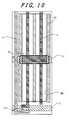
- FIG. 10illustrates a configuration of another embodiment of the liquid crystal display device according to the present invention, and is a plan view of one of a plurality of pixels in a liquid crystal display device of the so-called horizontal electric field type corresponding to FIG. 1 A.
- FIG. 10is similar to the embodiment illustrated in FIG. 5, except that the spacer 10 is formed to cover one of two electrodes forming a capacitor Cadd (an electrode extending integrally from the counter electrode 4 ), and thereby the area of the spacer 10 is made comparatively large.
- Caddan electrode extending integrally from the counter electrode 4
- the liquid crystal display device having this configurationprevents the galvanic corrosion of the covered electrode by the liquid crystal material as in the case of FIG. 9 .
- This embodimentcan increase the area of the spacer 10 without no reduction in the aperture ratio of the pixel, and improve reliability of the spacer.
- This embodimentalso provides an advantage of facilitating the control of the thickness of the liquid crystal layer (the spacing between the two transparent substrates) at the pixel because the spacer 10 is positioned approximately at the center of the dimension of the pixel in the y direction.
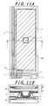
- FIGS. 11A and 11Billustrate a configuration of another embodiment of the liquid crystal display device according to the present invention.
- FIG. 11Ais a plan view of one of a plurality of pixels in a liquid crystal display device of the so-called vertical electric field type such as the twisted nematic type
- FIG. 11Bis a cross-sectional view of the pixel of FIG. 11A taken along line b—b of FIG. 11 A.
- the pixels as illustrated in FIGS. 11A and 11Bare arranged in the form of a matrix to constitute a display area.
- a liquid crystal display device of the vertical electric field type(commonly called the twisted nematic type)
- the transmission of light at each pixelis controlled by a vertical electric field applied across a layer of liquid crystal material sandwiched between opposing transparent electrodes formed on the inner surfaces of the opposing transparent substrates.
- Each pixelis formed by two electrodes formed on a pair of opposing substrates, respectively.
- U.S. Pat. No. 3,918,796, issued to Fergason on Nov. 11, 1975is hereby incorporated by reference.
- the configurations of the gate lines 2 , the drain lines 3 and the thin film transistors TFTare approximately similar to those in the above-explained liquid crystal display device of the horizontal electric field type.
- the differencesare that, in the liquid crystal display device of the vertical electric field type, the pixel electrodes 5 connected to the source electrode of the respective thin film transistors TFT are transparent films made of ITO (Indium-Tin-Oxide), for example, and are formed over the entire areas serving as the effective pixel areas (at least areas surrounded by the black matrix BM).
- ITOIndium-Tin-Oxide
- the counter electrode 4 Ais formed on the filter substrate 1 B to oppose the pixel electrodes 5 in common (sometimes called a common electrode for this relationship) and is made of ITO, for example.
- liquid crystal display device of this typeLight transmission through the liquid crystal layer is controlled by electric fields generated in a direction approximately perpendicular to the electrodes 5 , 4 A sandwiching the liquid crystal layer, and this is the reason why the liquid crystal display device of this type is called a liquid crystal display device of the vertical field type.
- the spacer 10is formed on the filter substrate 1 B so as to oppose approximately the center of the pixel electrode 5 .
- the spacer 10is formed on the planarizing film 8 by shaping the synthetic resin film coated on the planarizing film 8 using a photolithographic technique (and also by selective etching, if necessary) such that a truncated quadrilateral pyramid is left on the planarizing film 8 .
- the counter electrode 4 A and the orientation film 11are coated on the planarizing film 8 including the spacer 10 sequentially.
- the orientation film 11 formed on the side wall of the spacer 10is not parallel with the orientation film 7 formed on the TFT substrate 1 A.
- the configurationis such that, in the majority of the pixel area, electric fields are generated perpendicularly to the major surfaces of the substrates, but in the vicinity of the spacer 10 electric fields are generated in a direction at an angle from the normal to the major surfaces as shown in FIG. 11B, and this provides the above-explained multi-domain effect.
- This multi-domain effecteliminates the problem that the reversal in transmitted light intensity through the liquid crystal layer occurs at viewing angles deviating considerably from the main anticipated viewing angle of the liquid crystal panel due to the angular dependence of the electro-optic characteristics of the liquid crystal layer.
- This advantageis obtained by forming the spacer 10 within the effective pixel area (an area surrounded by the black matrix BM) without the need for increasing the number of the manufacturing steps.
- one spaceris disposed in each pixel, but the present invention is not limited to this arrangement.
- the present inventioncan be configured such that three spacers 10 are arranged along the long sides of the pixel.
- FIGS. 13A and 13Billustrate a configuration of another embodiment of the liquid crystal display device according to the present invention.
- FIG. 13Ais a plan view of one of a plurality of pixels in a liquid crystal display device of the so-called vertical electric field type such as the twisted nematic type
- FIG. 13Bis a cross-sectional view of the pixel of FIG. 13A taken along line b—b of FIG. 13 A.
- FIGS. 13A and 13Bcorrespond to FIGS. 11A and 11B, respectively.
- FIGS. 13A and 13Bis similar to the embodiment illustrated in FIGS. 11A and 11B, except that the pixel electrode 5 formed on the substrate opposing the substrate having the spacer 10 formed thereon is formed with an opening 5 h facing the spacer 10 .
- the opening 5 h in the pixel electrode 5is centered on the top surface of the spacer 10 and is larger in area than the top surface of the spacer 10 . This configuration prevents unexpected short circuit between the pixel electrode 5 and the counter electrode 4 A occurring even if the orientation films 11 , 7 are interposed therebetween.
- the pixel electrode 5is configured so as to be absent at an area facing the spacer 10 , and therefore the configuration of the present invention is not limited to the opening, but the configuration such as a cutout can also be employed. The similar configurations can be employed even if a plurality of spacers 10 are arranged in a pixel.
- FIGS. 14A and 14Bcorresponding to FIGS. 12A and 12B, respectively, three openings are provided in three portions facing the three spacers 10 , respectively, of the pixel electrode 5 .
- FIG. 15illustrates a configuration of another embodiment of the liquid crystal display device according to the present invention, and is a plan view of one of a plurality of pixels in a liquid crystal display device of the so-called vertical electric field type such as the twisted nematic type.
- This embodimentaims at heightening the multi-domain effect, and the spacer formed within one pixel area is configured so as to have a portion extending along the long sides of the pixel area and portions extending along the short sides of the pixel area.
- the spacer of this configurationhas the shape extending along respective directions, and thereby increases the area capable of producing the multi-domain effect and heightens the multi-domain effect.
- the spacerin each of two regions obtained by subdividing the pixel area in horizontal and vertical directions, is shaped to be symmetrical so that the regions for producing the multi-domain effect are distributed uniformly over the entire pixel, and consequently, the quality of displayed images can be improved.
- the spaceris shaped to be symmetrical.
- FIGS. 17A and 17Billustrate a configuration of another embodiment of the liquid crystal display device according to the present invention.
- FIG. 17Ais a plan view of one of a plurality of pixels in a liquid crystal display device of the so-called vertical electric field type such as the twisted nematic type
- FIG. 17Bis a cross-sectional view of the pixel of FIG. 17A taken along line b—b of FIG. 17 A.
- FIGS. 17A and 17Bcorrespond to FIGS. 11A and 11B, respectively.
- FIGS. 11A and 11Btakes advantage of the so-called multi-domain effect, but the present embodiment aims at masking the domains.
- the light-blocking film 15is formed on the filter substrate 1 B having the spacer 10 formed thereon such that the light-blocking film 15 is centered on the bottom surface of he spacer 10 and is larger in area than the bottom surface of the spacer 10 .
- the light-blocking film 15is made of the same material as the black matrix BM and is formed simultaneously with the black matrix BM.
- FIG. 18Ais a plan view of a modification of the present embodiment
- FIG. 18Bis a cross-sectional view of the pixel of FIG. 18A taken along line b—b of FIG. 18 A.
- This modificationaims at masking the domains occurring around the spacer 10 by light-blocking films 17 formed on the TFT substrate 1 A so as to ensure reliability.
- the light-blocking film 17 formed on the TFT substrate 1 Ais made of a metallic layer in this modification, and is formed of the same material as the gate line 2 and simultaneously with the gate line 2 , for example.
- the light-blocking film 17is annular so as to mask light from the side wall of the spacer 10 , but it is not always limited to such a shape, and the light-blocking film 17 of the same shape as the light-blocking film 15 can be employed.
- FIG. 19illustrates a configuration of another embodiment of the liquid crystal display device according to the present invention, and is a plan view of the spacer 10 employed in this embodiment.
- the spacer 10 of this embodimentcan be employed as the spacers in the previous embodiments and other liquid crystal display devices.
- the spacer 10is of the truncated quadrilateral pyramidal shape having a large-area base on the substrate side thereof and a small-area top surface 10 A. That is to say, the spacer 10 is flaring and has tapering side walls.
- the spacer 10is provided with a cutout 10 C which extends on a side wall from the center of one of four sides of its top surface 10 A to the center of a corresponding one of four sides of its base.
- a recess 10 Dis sometimes formed at the central portion of the top surface 10 A of the spacer 10 .
- the recess 10 Dmay be formed by shrinkage when the spacer is cured or due to indentation in the substrate having the spacer formed thereon.
- Airis sealed in the recess 10 D when the spacer having the recess 10 D on one substrate is pressed against the other substrate to assemble the liquid crystal panel, and the air is difficult to evacuate in the operation of filling the liquid crystal material into the space between the two substrates.
- the airpenetrates into the liquid crystal layer in the form of bubbles due to vibrations or shocks and changes the specific resistance of the liquid crystal material.
- This embodimentaims at evacuating completely the air easily contained between the top surface 10 A of the spacer 10 and the other substrate against which the top surface 10 A is pressed, by providing the cutout 10 c in the spacer 10 as explained in connection with FIG. 20 . That is to say, the cutout 10 C serves as means for evacuating the air from the recess 10 D and as a path for the liquid crystal material to penetrate into the recess 10 D.
- means for evacuating the airis in the form of the cutout 10 C of the above configuration, but means for evacuating the air may be in the form of a groove or indentation formed in the top surface 10 A of the spacer 10 , for example, or in the form of a groove or indentation traversing the top surface 10 A.
- the shape of the spacer 10is not limited to the above configuration, but it may be a circle or others in a plan view.
- FIG. 21illustrates a configuration of another embodiment of the liquid crystal display device according to the present invention, and is a fragmentary perspective view of the spacer 10 and its vicinity in this embodiment.
- This embodimentaims at evacuating the air between the spacer 10 and the substrate against which the spacer is pressed as in Embodiment 12, and in this embodiment the substrate pressed against the spacer 10 is configured for the object.
- a groove or indentation 15is formed in a portion of the protective film PAS on the substrate which is pressed against the spacer 10 such that the groove or indentation extends beyond the contact area between the spacer 10 and the protective film PAS.
- the groove or indentation 15serves as means for evacuating the air contained between the top surface 10 A of the spacer 10 and the substrate against which the top surface 10 A is pressed.
- FIG. 22is a plan view of another embodiment of the liquid crystal display device according to the present invention.
- a filling hole 21 for the liquid crystal materialis provided in a sealing member 20 for sealing the liquid crystal material between the substrates 1 A and 1 B, and the means for evacuating the air as explained in the previous embodiments is provided in the spacer 10 disposed in an area enclosed by the sealing member 20 or in the substrate against which the spacer 10 is pressed.
- the exit for the air of the means for evacuating the air, the cutout 10 C, for example,is directed toward the filling hole 21 for the liquid crystal material.
- This configurationenables efficient evacuation of the air contained between the spacer 10 and the substrate against which the spacer 10 is pressed, via the above-explained means for evacuating the air, because the filling hole 21 for the liquid crystal material serves as the exit for evacuating air from the space between the two substrates as well as the hole for filling the liquid crystal material into a space between the two substrates, and consequently, the air contained between the spacer 10 and the substrate is directed directly into the filling hole 21 without going around the spacer 10 .
- FIG. 23illustrates a configuration of another embodiment of the liquid crystal display device according to the present invention, and is a perspective view of the spacer 10 in this embodiment.
- the spacer 10is subdivided into plural spacer pieces, and in other words, the spacer 10 comprises a group of subdivided spacers.
- the spacer 10 having this configurationhas a function of evacuating the air as in the previous embodiments, and also is provided with resiliency.
- the spacer 10is subject to strong force applied by the substrate, but the spacer 10 can prevent its breakage with its resiliency.
- the subdivision of the spacer 10is applied to at least the top portion of the spacer 10 as shown in FIG. 24 .
- FIG. 25illustrates a configuration of another embodiment of the liquid crystal display device of the horizontal electric field type according to the present invention, and is a cross-sectional view of the liquid crystal display device taken along one of its gate lines.
- the spacers 10are fixed on the filter substrate 1 B opposing the TFT substrate 1 A, and comprise a first type of spacers 10 B disposed in a region 25 B in FIG. 25 for maintaining the spacing between the two substrates 1 A, 1 B and a second type of spacers 10 A disposed so as to be superposed on both the ends of each of the gate lines in a region 25 A in FIG. 25 .
- a plurality of strip-shaped conductive layers 21are formed on the surface of the filter substrate 1 B facing toward the liquid crystal layer such that each of the strip-shaped conductive layers 21 is superposed on a respective one of the gate lines 2 formed on the TFT substrate 1 A, and consequently, each of the strip-shaped conductive layers 21 covers a pair of the second type of spacers 10 A corresponding to one of the gate lines 2 and is electrically connected with the corresponding one of the gate lines 2 .
- This configurationprovides a redundant circuit for each of the gate lines 2 and provides protection against unintentional line breaks in the gate lines 2 .
- the redundant circuitsare provided to the gate lines 2 , the above configuration is also applicable to protection against the line breaks in the drain lines 3 by interchanging the gate line 2 with the drain line 3 in FIG. 25 .
- This embodimentis also applicable to the previous embodiments of the liquid crystal display device of the horizontal electric field type.
- FIG. 26illustrates a configuration of another embodiment of the liquid crystal display device of the vertical electric field type according to the present invention, and is a cross-sectional view of the liquid crystal display device taken along one of the gate lines 2 .
- the spacers 10are fixed on the filter substrate 1 B opposing the TFT substrate 1 A, and comprise a first type of spacers 10 B disposed in a region 26 B in FIG. 26 for maintaining the spacing between the two substrates 1 A, 1 B and a third type of spacers 10 A disposed in the vicinity of the sealing member 20 for sealing the two substrates 1 A, 1 B in a region 26 A in FIG. 26 .
- the third type of spacers 10 Aare formed simultaneously with the first type of spacers 10 B.
- a common electrode (a transparent electrode) 22 facing the plural pixels in commonis formed on the surface of the filter substrate 1 B facing toward the liquid crystal layer including the surfaces of the spacers 10 .
- a conductive layer 23is formed on a region of the TFT substrate 1 A against which the third type spacer 10 A is pressed, such that the conductive layer 23 covers the third type spacer 10 A and is electrically connected with the common electrode 22 .
- the conductive layer 23extends beyond the sealing member 20 on the TFT substrate 1 A so as to be connected to a terminal for supplying a reference voltage to the common electrode 22 .
- the reference voltage supplied to the terminal on the TFT substrate 1 Ais applied to the common electrode 22 on the filter substrate 1 B via the third type spacer 10 A.
- the liquid crystal display device of this configurationeliminates the need for providing an additional connecting means for bringing out the connection of the common electrode 22 onto the surface of the TFT substrate 1 A.
- the present embodimentis also applicable to the previous embodiments of the liquid crystal display device of the vertical electric field type.
- spacersare fixed on the TFT substrate or the filter substrate.
- fixation of the spacers on the filter substraterequires an additional process step of selective etching for forming the spacers by a photolithographic technique, and chemicals used in the etching process may cause deterioration of the thin film transistors.
- FIG. 27is a detailed cross-sectional view of the spacer 10 fabricated on and fixed to the filter substrate 1 B.
- the black matrix BM and the color filter FILare formed on the surface of the filter substrate 1 B on the liquid crystal layer side thereof, and then the planarizing film 8 made of thermosetting resin is formed on the black matrix BM and the color filter FIL for planarizing the top surface of the filter substrate 1 B.
- the spacer 10 made of photocuring resinis positioned at a predetermined position on the planarizing film 8 .
- Fabrication of the spacer 10 by using photocuring resineliminates the need for the process step of selective etching, resulting in the reduction of the number of the process steps.
- This embodimentis also applicable to the previous embodiments.
- This embodimentis not limited to fabrication of the spacers on the filter substrate 1 B, but also is applicable to fabrication of the spacers on the TFT substrate 1 A.
- FIG. 28Ais a plan view of the arrangement of the spacers 10 superposed on the black matrix BM for defining the contours of the pixels in the display area.
- the spacers 10are distributed uniformly over the entire display area, and each of the spacers 10 is allotted to a group comprising the equal number of adjacent pixels.
- the number of the spacers 10 disposed in the display areais reduced so as to reduce the orientation defects caused by the spacers 10 . This prevents occurrence of unintentional contrast produced by light leakage, especially in displaying of a black image.
- FIG. 28Bis a plan view of the arrangement of the spacers 10 superposed on the black matrix BM in the display area.
- the number of the spacers 10 disposed in the display areais reduced as in Embodiment 20, but the difference is that spacers are arranged randomly, instead of being arranged uniformly.
- the repeating pattern of light leakageis easily discernible to the human eye, and therefore the problem with the light leakage is solved by arranging the spacers randomly.
- FIG. 29illustrates a configuration of another embodiment of the liquid crystal display device according to the present invention, and is a view similar to that of FIG. 1 B.
- the spacer 10is fixed to the substrate 1 B and the substrate 1 A is superposed on the substrate 1 B, and an adhesive 30 is interposed between the spacer 10 and a region of the transparent substrate 1 A against which the spacer 10 is pressed.
- the adhesive 30is not interposed between the spacer 10 and the substrate 1 A, then, in the contact area between the spacer 10 and the substrate 1 A, both the surfaces of the spacer 10 and the substrate 1 A are covered with the orientation films made of the same material, respectively, and there arises a problem that adhesion between the two surfaces is weak.
- a Si coupling agentfor example, the reliability in maintaining the spacing between the two substrates is secured.
- the substrate 1 B with the surfaces of the spacers 10 coated with the adhesive agent 30is obtained.
- the substrate 1 B with the surfaces of the spacers 10 coated with the adhesive agent 30is obtained.
- This embodimentis also applicable to the previous embodiments.
- FIG. 32illustrates a configuration of another embodiment of the liquid crystal display device according to the present invention, and is a view similar to that of FIG. 1 B.
- a recess 40is formed on the substrate 1 A opposing the substrate 1 B having the spacer 10 fixed thereto such that the top of the spacer 10 is driven into the recess 40 .
- the recess 40is formed in the protective film PAS on the TFT substrate 1 A, for example, and has a flaring cross section. With this configuration, the top of the spacer 10 is forced into the recess 40 and is fastened tightly to the TFT substrate 1 A as bonded with an adhesive agent.
- FIG. 33illustrates a configuration of another embodiment of the liquid crystal display device according to the present invention.
- a groove corresponding to the recess 40 in FIG. 32is formed by a pair of signal lines (or wiring lines) 42 .
- the opposing side walls of the two signal linesare tapered in the opposite directions.
- the configuration of this embodimentis such that the top of the spacer 10 is forced into the recess, but the present invention is not limited to this configuration.
- This combination of the spacer 10 and the recess or the groovealso serves as means for aligning the opposing two substrates with each other.
- the liquid crystal display device according to the present inventioncan improve the quality of displayed images.
Landscapes
- Physics & Mathematics (AREA)
- Nonlinear Science (AREA)
- Crystallography & Structural Chemistry (AREA)
- Mathematical Physics (AREA)
- Chemical & Material Sciences (AREA)
- General Physics & Mathematics (AREA)
- Optics & Photonics (AREA)
- Life Sciences & Earth Sciences (AREA)
- Environmental Sciences (AREA)
- Mycology (AREA)
- Spectroscopy & Molecular Physics (AREA)
- Geometry (AREA)
- Liquid Crystal (AREA)
Abstract
Description


Claims (14)
Priority Applications (5)
| Application Number | Priority Date | Filing Date | Title |
|---|---|---|---|
| US10/228,320US6798486B2 (en) | 1999-04-14 | 2002-08-27 | Liquid crystal display device with spacers formed on a planarizing film disposed over color filters |
| US10/365,629US7167228B2 (en) | 1999-04-14 | 2003-02-13 | Liquid crystal display device with two kinds of projected portions on a substrate |
| US10/892,299US7050140B2 (en) | 1999-04-14 | 2004-07-16 | Liquid crystal display device with spacers formed on a planarizing film disposed over color filters |
| US11/589,952US7751020B2 (en) | 1999-04-14 | 2006-10-31 | Liquid crystal display device with two kinds of projected portions on a substrate |
| US12/285,413US7643119B2 (en) | 1999-04-14 | 2008-10-03 | Liquid crystal display device having improved spacers |
Applications Claiming Priority (4)
| Application Number | Priority Date | Filing Date | Title |
|---|---|---|---|
| JP11-106382 | 1999-04-14 | ||
| JP10638399AJP3795252B2 (en) | 1999-04-14 | 1999-04-14 | Liquid crystal display |
| JP11-106383 | 1999-04-14 | ||
| JP10638299AJP3833844B2 (en) | 1999-04-14 | 1999-04-14 | Liquid crystal display |
Related Child Applications (2)
| Application Number | Title | Priority Date | Filing Date |
|---|---|---|---|
| US10/228,320ContinuationUS6798486B2 (en) | 1999-04-14 | 2002-08-27 | Liquid crystal display device with spacers formed on a planarizing film disposed over color filters |
| US10/365,629ContinuationUS7167228B2 (en) | 1999-04-14 | 2003-02-13 | Liquid crystal display device with two kinds of projected portions on a substrate |
Publications (1)
| Publication Number | Publication Date |
|---|---|
| US6583846B1true US6583846B1 (en) | 2003-06-24 |
Family
ID=26446491
Family Applications (6)
| Application Number | Title | Priority Date | Filing Date |
|---|---|---|---|
| US09/542,870Expired - LifetimeUS6583846B1 (en) | 1999-04-14 | 2000-04-04 | Liquid crystal display device with spacer covered with an electrode |
| US10/228,320Expired - LifetimeUS6798486B2 (en) | 1999-04-14 | 2002-08-27 | Liquid crystal display device with spacers formed on a planarizing film disposed over color filters |
| US10/365,629Expired - LifetimeUS7167228B2 (en) | 1999-04-14 | 2003-02-13 | Liquid crystal display device with two kinds of projected portions on a substrate |
| US10/892,299Expired - LifetimeUS7050140B2 (en) | 1999-04-14 | 2004-07-16 | Liquid crystal display device with spacers formed on a planarizing film disposed over color filters |
| US11/589,952Expired - Fee RelatedUS7751020B2 (en) | 1999-04-14 | 2006-10-31 | Liquid crystal display device with two kinds of projected portions on a substrate |
| US12/285,413Expired - Fee RelatedUS7643119B2 (en) | 1999-04-14 | 2008-10-03 | Liquid crystal display device having improved spacers |
Family Applications After (5)
| Application Number | Title | Priority Date | Filing Date |
|---|---|---|---|
| US10/228,320Expired - LifetimeUS6798486B2 (en) | 1999-04-14 | 2002-08-27 | Liquid crystal display device with spacers formed on a planarizing film disposed over color filters |
| US10/365,629Expired - LifetimeUS7167228B2 (en) | 1999-04-14 | 2003-02-13 | Liquid crystal display device with two kinds of projected portions on a substrate |
| US10/892,299Expired - LifetimeUS7050140B2 (en) | 1999-04-14 | 2004-07-16 | Liquid crystal display device with spacers formed on a planarizing film disposed over color filters |
| US11/589,952Expired - Fee RelatedUS7751020B2 (en) | 1999-04-14 | 2006-10-31 | Liquid crystal display device with two kinds of projected portions on a substrate |
| US12/285,413Expired - Fee RelatedUS7643119B2 (en) | 1999-04-14 | 2008-10-03 | Liquid crystal display device having improved spacers |
Country Status (3)
| Country | Link |
|---|---|
| US (6) | US6583846B1 (en) |
| KR (2) | KR100375239B1 (en) |
| TW (1) | TW498177B (en) |
Cited By (42)
| Publication number | Priority date | Publication date | Assignee | Title |
|---|---|---|---|---|
| US20020033927A1 (en)* | 2000-08-14 | 2002-03-21 | Joong-Hyun Mun | Liquid crystal display and a method for fabricating the same |
| US20020075442A1 (en)* | 2000-12-18 | 2002-06-20 | Hitachi, Ltd. | Liquid crystal display device |
| US20020089636A1 (en)* | 2000-12-22 | 2002-07-11 | Lg.Philips Lcd Co., Ltd. | Liquid crystal display device |
| US20030043319A1 (en)* | 2001-08-28 | 2003-03-06 | Hitachi, Ltd. | Liquid crystal display device |
| US20030071959A1 (en)* | 2001-06-05 | 2003-04-17 | Yoshihide Koyama | Liquid crystal display device and liquid crystal display apparatus incorporating the same |
| US20030117572A1 (en)* | 2001-12-20 | 2003-06-26 | Fujitsu Display Technologies Corporation | Display device and its manufacture |
| US20040004607A1 (en)* | 2002-07-01 | 2004-01-08 | Chi Mei Optoelectronics Corp. | Image display element and image display device |
| US20040100611A1 (en)* | 2000-10-04 | 2004-05-27 | Song Jang-Kun | Liquid crystal display |
| US20040169797A1 (en)* | 2003-02-21 | 2004-09-02 | Seiko Epson Corporaton | Electro-optical panel and electronic equipment |
| US20040189928A1 (en)* | 2003-03-28 | 2004-09-30 | Yong-Ho Yang | Spacers for display devices |
| US20040227891A1 (en)* | 2003-05-14 | 2004-11-18 | Naoto Hirota | High quality and ultra large screen liquid crystal display device and production method thereof |
| US20040246410A1 (en)* | 2003-06-09 | 2004-12-09 | Samsung Electronics Co., Ltd. | Panel for display device and liquid crystal display |
| US20040263764A1 (en)* | 2003-06-24 | 2004-12-30 | Kim Jeong Hyun | Liquid crystal display panel and method of fabricating the same |
| US20050140856A1 (en)* | 2003-12-27 | 2005-06-30 | Lg Philips Lcd Co., Ltd. | Liquid crystal display device and method for fabricating the ssme |
| US20050185129A1 (en)* | 2004-02-25 | 2005-08-25 | Lg.Philips Lcd Co., Ltd. | Liquid crystal display device and method of fabricating the same |
| US20050200777A1 (en)* | 2001-08-22 | 2005-09-15 | Shingo Nagano | Liquid crystal display device |
| US20050243247A1 (en)* | 2004-04-30 | 2005-11-03 | Lg.Philips Lcd Co., Ltd. | Liquid crystal display device having patterned spacers and method of fabricating the same |
| US20050264749A1 (en)* | 2004-05-29 | 2005-12-01 | Lg.Philips Lcd Co. Ltd. | Liquid crystal display panel and method for fabricating the same |
| US20050270471A1 (en)* | 2004-06-03 | 2005-12-08 | Hideki Kitagawa | Liquid crystal display device |
| US20060038937A1 (en)* | 2004-08-12 | 2006-02-23 | Seiko Epson Corporation | Electro-optical device, method of manufacturing the same, and electronic apparatus |
| US20060103803A1 (en)* | 2002-08-02 | 2006-05-18 | Baek-Kyun Jeon | Panel for liquid crystal display, liquid crystal display including the panel, and methods for manufacturing the same |
| US20060139550A1 (en)* | 2000-04-19 | 2006-06-29 | Jang-Jin Yoo | In-plane switching LCD panel |
| US20060221294A1 (en)* | 2005-04-01 | 2006-10-05 | Innolux Display Corp. | Liquid crystal display device and method for manufacturing the same |
| US7133108B2 (en)* | 2000-12-08 | 2006-11-07 | Hitachi, Ltd. | Liquid crystal display device |
| US7167228B2 (en)* | 1999-04-14 | 2007-01-23 | Hitachi, Ltd. | Liquid crystal display device with two kinds of projected portions on a substrate |
| US20070159588A1 (en)* | 2006-01-11 | 2007-07-12 | Samsung Electronics Co., Ltd. | Color filter substrate and liquid crystal display panel comprising the same |
| US20070195249A1 (en)* | 2000-11-22 | 2007-08-23 | Joong-Hyun Mun | Liquid crystal display having wide viewing angle |
| US20070222934A1 (en)* | 2006-03-24 | 2007-09-27 | Quanta Display Inc. | Method for manufacturing LCD panel |
| US20070247579A1 (en)* | 2006-04-19 | 2007-10-25 | Cho Seon-Ah | Liquid crystal display |
| US20070291210A1 (en)* | 2006-06-19 | 2007-12-20 | Samsung Electronics Co., Ltd. | Color filter substrate, display panel having the same, and method for manufacturing the same |
| US20080239230A1 (en)* | 2003-03-07 | 2008-10-02 | Semiconductor Energy Laboratory Co., Ltd. | Liquid crystal display device and method for manufacturing the same |
| US20090092446A1 (en)* | 2007-10-08 | 2009-04-09 | Hilti Aktiengesellschaft | Fastening element |
| US20090147207A1 (en)* | 2007-12-10 | 2009-06-11 | Seiko Epson Corporation | Liquid crystal device and method for manufacturing the same |
| US20090303407A1 (en)* | 2004-04-30 | 2009-12-10 | Dong-Hoon Lee | Liquid crystal display device and method of fabricating the same |
| US20100155731A1 (en)* | 2008-12-24 | 2010-06-24 | Boe Technology Group Co., Ltd. | Touching-type electronic paper and method for manufacturing the same |
| US20100265450A1 (en)* | 2006-06-13 | 2010-10-21 | Hsiang-Pin Fan | Placement of spacers in a liquid crystal display panel |
| US20110285023A1 (en)* | 2010-05-20 | 2011-11-24 | Taiwan Semiconductor Manufacturing Company, Ltd. | Substrate Interconnections having Different Sizes |
| US9105530B2 (en) | 2012-09-18 | 2015-08-11 | Taiwan Semiconductor Manufacturing Company, Ltd. | Conductive contacts having varying widths and method of manufacturing same |
| US9299674B2 (en) | 2012-04-18 | 2016-03-29 | Taiwan Semiconductor Manufacturing Company, Ltd. | Bump-on-trace interconnect |
| US9425136B2 (en) | 2012-04-17 | 2016-08-23 | Taiwan Semiconductor Manufacturing Company, Ltd. | Conical-shaped or tier-shaped pillar connections |
| US9646923B2 (en) | 2012-04-17 | 2017-05-09 | Taiwan Semiconductor Manufacturing Company, Ltd. | Semiconductor devices, methods of manufacture thereof, and packaged semiconductor devices |
| US10170714B2 (en)* | 2016-07-11 | 2019-01-01 | Au Optronics Corporation | Display panel |
Families Citing this family (21)
| Publication number | Priority date | Publication date | Assignee | Title |
|---|---|---|---|---|
| JP4244289B2 (en)* | 2002-10-31 | 2009-03-25 | シャープ株式会社 | Substrate for liquid crystal display device and liquid crystal display device including the same |
| KR100895306B1 (en)* | 2002-11-14 | 2009-05-07 | 삼성전자주식회사 | Substrate for Liquid Crystal Display |
| KR100892357B1 (en)* | 2002-12-09 | 2009-04-08 | 엘지디스플레이 주식회사 | Color filter substrate for liquid crystal display device and manufacturing method thereof |
| KR101080401B1 (en)* | 2004-04-23 | 2011-11-04 | 삼성전자주식회사 | Bonding structure of flat panel display, method of forming the same, and flat panel display comprising the same |
| KR20050105571A (en)* | 2004-04-30 | 2005-11-04 | 엘지.필립스 엘시디 주식회사 | Method of fabricating the color filter substrate for liquid crystal display device |
| KR100675635B1 (en)* | 2004-05-10 | 2007-02-02 | 엘지.필립스 엘시디 주식회사 | Transverse field mode liquid crystal display with improved contrast ratio |
| JP2006154168A (en)* | 2004-11-29 | 2006-06-15 | Seiko Epson Corp | Active matrix substrate, electro-optical device, electronic device, and manufacturing method of active matrix substrate |
| US7400373B2 (en)* | 2005-05-27 | 2008-07-15 | Hannstar Display Corp. | Liquid crystal display panel and method manufacturing the same having particular spacers |
| KR101192770B1 (en)* | 2005-06-30 | 2012-10-18 | 엘지디스플레이 주식회사 | Liquid Crystal Display Panel and Method of Fabricating the same |
| KR20070012084A (en)* | 2005-07-22 | 2007-01-25 | 삼성전자주식회사 | A color filter substrate, a liquid crystal display panel including the same, and a manufacturing method thereof |
| JP2008164787A (en) | 2006-12-27 | 2008-07-17 | Epson Imaging Devices Corp | Liquid crystal display device |
| US8077286B2 (en)* | 2007-08-10 | 2011-12-13 | Toshiba Matsushita Display Technology Co., Ltd. | Liquid crystal display device |
| JP2009058618A (en)* | 2007-08-30 | 2009-03-19 | Hitachi Displays Ltd | Liquid crystal display |
| JP4693131B2 (en)* | 2008-02-14 | 2011-06-01 | 東芝モバイルディスプレイ株式会社 | Liquid crystal display |
| JP5246782B2 (en) | 2008-03-06 | 2013-07-24 | 株式会社ジャパンディスプレイウェスト | Liquid crystal device and electronic device |
| WO2012147592A1 (en)* | 2011-04-25 | 2012-11-01 | シャープ株式会社 | Liquid crystal display panel and liquid crystal display device |
| JP5797487B2 (en)* | 2011-07-22 | 2015-10-21 | スタンレー電気株式会社 | Liquid crystal display |
| US20130250228A1 (en)* | 2012-03-26 | 2013-09-26 | Chiachiang Lin | LCD Panel, Manufacturing Method Thereof, and LCD Device |
| CN104297986B (en)* | 2014-10-08 | 2017-10-31 | 厦门天马微电子有限公司 | A kind of liquid crystal display panel and display device |
| TWI575284B (en)* | 2015-06-24 | 2017-03-21 | 群創光電股份有限公司 | Display panel |
| CN111584608B (en)* | 2020-06-08 | 2022-07-22 | 京东方科技集团股份有限公司 | OLED display substrate and manufacturing method thereof, display panel and display device |
Citations (11)
| Publication number | Priority date | Publication date | Assignee | Title |
|---|---|---|---|---|
| JPH0876131A (en) | 1994-09-05 | 1996-03-22 | Nippon Petrochem Co Ltd | Display device |
| JPH08114809A (en) | 1994-10-14 | 1996-05-07 | Sony Corp | Liquid crystal panel and its production |
| JPH1048636A (en) | 1996-08-05 | 1998-02-20 | Nec Corp | Liquid crystal display device |
| US5852485A (en)* | 1996-02-27 | 1998-12-22 | Sharp Kabushiki Kaisha | Liquid crystal display device and method for producing the same |
| US5949511A (en)* | 1996-11-20 | 1999-09-07 | Lg Electronics Inc. | Liquid crystal display |
| US5995186A (en)* | 1996-04-04 | 1999-11-30 | Lg Electronics Inc. | Parallel field liquid crystal display with substantially straight data and common electrodes inclined at an angle to a gate line |
| US6115098A (en)* | 1997-12-25 | 2000-09-05 | Sharp Kabushiki Kaisha | LCD having an LC layer with spacers arranged so that LC molecules are in axial symmetry upon application of voltage |
| US6211937B1 (en)* | 1997-10-06 | 2001-04-03 | Sharp Kabushiki Kaisha | Liquid crystal display device including spacers located in positions indicative of rubbing/orientation direction |
| US6317188B1 (en)* | 1999-04-20 | 2001-11-13 | Nec Corporation | LCD having particular spacing between spacers |
| US6341003B1 (en)* | 1998-01-23 | 2002-01-22 | Hitachi, Ltd. | Liquid crystal display device in which the pixel electrode crosses the counter electrode |
| US6356335B1 (en)* | 1998-11-11 | 2002-03-12 | Lg. Phillips Lcd Co., Ltd. | Multi-domain liquid crystal display device |
Family Cites Families (25)
| Publication number | Priority date | Publication date | Assignee | Title |
|---|---|---|---|---|
| US4385806A (en)* | 1978-06-08 | 1983-05-31 | Fergason James L | Liquid crystal display with improved angle of view and response times |
| JPH07104450B2 (en)* | 1990-10-17 | 1995-11-13 | スタンレー電気株式会社 | Biaxial optical element and manufacturing method thereof |
| JPH07225389A (en) | 1994-02-16 | 1995-08-22 | Matsushita Electric Ind Co Ltd | Liquid crystal display device and manufacturing method thereof |
| JP3005418B2 (en) | 1994-05-18 | 2000-01-31 | 三洋電機株式会社 | Liquid crystal display |
| JP3999824B2 (en)* | 1995-08-21 | 2007-10-31 | 東芝電子エンジニアリング株式会社 | Liquid crystal display element |
| JPH09120075A (en) | 1995-08-21 | 1997-05-06 | Toshiba Electron Eng Corp | Liquid crystal display device |
| TW373098B (en)* | 1995-09-06 | 1999-11-01 | Toshiba Corp | Liquid crystal exposure component and its fabricating method |
| JP3708593B2 (en) | 1995-09-06 | 2005-10-19 | 東芝電子エンジニアリング株式会社 | Liquid crystal display device and manufacturing method thereof |
| US6038006A (en)* | 1996-09-02 | 2000-03-14 | Casio Computer Co., Ltd. | Liquid crystal display device with light shield and color filter overlapping two edges of pixel electrode |
| JPH10123534A (en)* | 1996-10-23 | 1998-05-15 | Toshiba Corp | Liquid crystal display device |
| JPH10221694A (en) | 1996-12-06 | 1998-08-21 | Stanley Electric Co Ltd | Liquid crystal display device |
| GB2321718A (en) | 1997-01-31 | 1998-08-05 | Nat Science Council | LIquid crystal display |
| JP3966614B2 (en)* | 1997-05-29 | 2007-08-29 | 三星電子株式会社 | Wide viewing angle LCD |
| TW509808B (en)* | 1997-06-12 | 2002-11-11 | Sharp Kk | Liquid crystal display device |
| US6208402B1 (en)* | 1997-09-17 | 2001-03-27 | Citizen Watch Co., Ltd. | Antiferroelectric liquid crystal panel |
| JPH11119227A (en)* | 1997-10-13 | 1999-04-30 | Hitachi Ltd | Liquid crystal display |
| JPH11271718A (en)* | 1998-03-25 | 1999-10-08 | Sharp Corp | Liquid crystal display device, plasma addressed liquid crystal display device and method of manufacturing the same |
| JP2000019527A (en)* | 1998-06-30 | 2000-01-21 | Hitachi Ltd | Liquid crystal display |
| US6583846B1 (en)* | 1999-04-14 | 2003-06-24 | Hitachi, Ltd. | Liquid crystal display device with spacer covered with an electrode |
| JP2001005007A (en)* | 1999-06-18 | 2001-01-12 | Hitachi Ltd | Liquid crystal display |
| KR100709709B1 (en)* | 2000-07-27 | 2007-04-19 | 삼성전자주식회사 | Vertically Aligned Liquid Crystal Display |
| JP3936126B2 (en)* | 2000-08-30 | 2007-06-27 | シャープ株式会社 | Transflective liquid crystal display device |
| DE10152470B4 (en)* | 2000-11-23 | 2014-08-14 | Heidelberger Druckmaschinen Ag | Method for color presetting in multicolor printing |
| JP3793915B2 (en)* | 2001-02-28 | 2006-07-05 | 株式会社日立製作所 | Liquid crystal display |
| JP2005257883A (en)* | 2004-03-10 | 2005-09-22 | Nec Lcd Technologies Ltd | Liquid crystal display |
- 2000
- 2000-04-04USUS09/542,870patent/US6583846B1/ennot_activeExpired - Lifetime
- 2000-04-10TWTW089106640Apatent/TW498177B/ennot_activeIP Right Cessation
- 2000-04-10KRKR10-2000-0018592Apatent/KR100375239B1/ennot_activeExpired - Fee Related
- 2002
- 2002-05-24KRKR10-2002-0029015Apatent/KR100396638B1/ennot_activeExpired - Fee Related
- 2002-08-27USUS10/228,320patent/US6798486B2/ennot_activeExpired - Lifetime
- 2003
- 2003-02-13USUS10/365,629patent/US7167228B2/ennot_activeExpired - Lifetime
- 2004
- 2004-07-16USUS10/892,299patent/US7050140B2/ennot_activeExpired - Lifetime
- 2006
- 2006-10-31USUS11/589,952patent/US7751020B2/ennot_activeExpired - Fee Related
- 2008
- 2008-10-03USUS12/285,413patent/US7643119B2/ennot_activeExpired - Fee Related
Patent Citations (11)
| Publication number | Priority date | Publication date | Assignee | Title |
|---|---|---|---|---|
| JPH0876131A (en) | 1994-09-05 | 1996-03-22 | Nippon Petrochem Co Ltd | Display device |
| JPH08114809A (en) | 1994-10-14 | 1996-05-07 | Sony Corp | Liquid crystal panel and its production |
| US5852485A (en)* | 1996-02-27 | 1998-12-22 | Sharp Kabushiki Kaisha | Liquid crystal display device and method for producing the same |
| US5995186A (en)* | 1996-04-04 | 1999-11-30 | Lg Electronics Inc. | Parallel field liquid crystal display with substantially straight data and common electrodes inclined at an angle to a gate line |
| JPH1048636A (en) | 1996-08-05 | 1998-02-20 | Nec Corp | Liquid crystal display device |
| US5949511A (en)* | 1996-11-20 | 1999-09-07 | Lg Electronics Inc. | Liquid crystal display |
| US6211937B1 (en)* | 1997-10-06 | 2001-04-03 | Sharp Kabushiki Kaisha | Liquid crystal display device including spacers located in positions indicative of rubbing/orientation direction |
| US6115098A (en)* | 1997-12-25 | 2000-09-05 | Sharp Kabushiki Kaisha | LCD having an LC layer with spacers arranged so that LC molecules are in axial symmetry upon application of voltage |
| US6341003B1 (en)* | 1998-01-23 | 2002-01-22 | Hitachi, Ltd. | Liquid crystal display device in which the pixel electrode crosses the counter electrode |
| US6356335B1 (en)* | 1998-11-11 | 2002-03-12 | Lg. Phillips Lcd Co., Ltd. | Multi-domain liquid crystal display device |
| US6317188B1 (en)* | 1999-04-20 | 2001-11-13 | Nec Corporation | LCD having particular spacing between spacers |
Cited By (121)
| Publication number | Priority date | Publication date | Assignee | Title |
|---|---|---|---|---|
| US7751020B2 (en) | 1999-04-14 | 2010-07-06 | Hitachi, Ltd. | Liquid crystal display device with two kinds of projected portions on a substrate |
| US7167228B2 (en)* | 1999-04-14 | 2007-01-23 | Hitachi, Ltd. | Liquid crystal display device with two kinds of projected portions on a substrate |
| US20070040984A1 (en)* | 1999-04-14 | 2007-02-22 | Hitachi, Ltd. | Liquid crystal display device with two kinds of projected portions on a substrate |
| US7643119B2 (en) | 1999-04-14 | 2010-01-05 | Hitachi, Ltd. | Liquid crystal display device having improved spacers |
| US20060139550A1 (en)* | 2000-04-19 | 2006-06-29 | Jang-Jin Yoo | In-plane switching LCD panel |
| US7440061B2 (en)* | 2000-04-19 | 2008-10-21 | Lg Display Co., Ltd. | In-plane switching LCD panel |
| US20070263163A1 (en)* | 2000-08-14 | 2007-11-15 | Samsung Electronics Co., Ltd. | Liquid crystal display and a method for fabricating the same |
| US8319929B2 (en) | 2000-08-14 | 2012-11-27 | Samsung Display Co., Ltd. | Liquid crystal display including a variable width spacer element and method for fabricating the same |
| US7639337B2 (en) | 2000-08-14 | 2009-12-29 | Samsung Electronics Co., Ltd. | Liquid crystal display and method for fabricating the same |
| US20100053485A1 (en)* | 2000-08-14 | 2010-03-04 | Joong-Hyun Mun | Liquid crystal display and method for fabricating the same |
| US7486364B2 (en) | 2000-08-14 | 2009-02-03 | Samsung Electronics Co., Ltd. | Liquid crystal display and a method for fabricating the same |
| US9577103B2 (en)* | 2000-08-14 | 2017-02-21 | Samsung Display Co., Ltd. | Liquid crystal display including a variable width spacer element and method for fabricating the same |
| US20140054591A1 (en)* | 2000-08-14 | 2014-02-27 | Samsung Display Co., Ltd | Liquid crystal display including a variable width spacer element and method for fabricating the same |
| US7057695B2 (en)* | 2000-08-14 | 2006-06-06 | Samsung Electronics Co., Ltd. | Liquid crystal display having protrusions with different thicknesses |
| US20080284964A1 (en)* | 2000-08-14 | 2008-11-20 | Joong-Hyun Mun | Liquid crystal display and a method for fabricating the same |
| US8599354B2 (en) | 2000-08-14 | 2013-12-03 | Samsung Display Co., Ltd. | Liquid crystal display including a variable width spacer element |
| US20090128725A1 (en)* | 2000-08-14 | 2009-05-21 | Joong-Hyun Mun | Liquid crystal display and method for fabricating the same |
| US20060158600A1 (en)* | 2000-08-14 | 2006-07-20 | Samsung Electronics, Co., Ltd. | Liquid crystal display and a method for fabricating the same |
| US7525621B2 (en)* | 2000-08-14 | 2009-04-28 | Samsung Electronics, Co., Ltd. | Liquid crystal display and a method for fabricating the same |
| US20020033927A1 (en)* | 2000-08-14 | 2002-03-21 | Joong-Hyun Mun | Liquid crystal display and a method for fabricating the same |
| US8009257B2 (en) | 2000-08-14 | 2011-08-30 | Samsung Electronics Co., Ltd. | Liquid crystal display including a spacer and passivation formed of the same material |
| US20110037933A1 (en)* | 2000-08-14 | 2011-02-17 | Samsung Electronics Co., Ltd. | Liquid crystal display including a spacer element and method for fabricating the same |
| US7843542B2 (en)* | 2000-08-14 | 2010-11-30 | Samsung Electronics Co., Ltd. | Liquid crystal display including a spacer element and method for fabricating the same |
| US20060209245A1 (en)* | 2000-08-14 | 2006-09-21 | Joong-Hyun Mun | Liquid crystal display and a method for fabricating the same |
| US7830492B2 (en) | 2000-08-14 | 2010-11-09 | Samsung Electronics Co., Ltd. | Liquid crystal display and method for fabricating the same |
| US20040100611A1 (en)* | 2000-10-04 | 2004-05-27 | Song Jang-Kun | Liquid crystal display |
| US7247411B2 (en)* | 2000-10-04 | 2007-07-24 | Samsung Electronics Co., Ltd. | Liquid crystal display |
| US20070195249A1 (en)* | 2000-11-22 | 2007-08-23 | Joong-Hyun Mun | Liquid crystal display having wide viewing angle |
| US7564526B2 (en) | 2000-11-22 | 2009-07-21 | Samsung Electronics Co., Ltd. | Liquid crystal display having wide viewing angle |
| US20070024797A1 (en)* | 2000-12-08 | 2007-02-01 | Hitachi, Ltd. | Liquid crystal display device |
| US7133108B2 (en)* | 2000-12-08 | 2006-11-07 | Hitachi, Ltd. | Liquid crystal display device |
| US7456926B2 (en) | 2000-12-08 | 2008-11-25 | Hitachi, Ltd. | Liquid crystal display device |
| US20080266511A1 (en)* | 2000-12-08 | 2008-10-30 | Hitachi, Ltd. | Liquid crystal display device |
| US7826028B2 (en) | 2000-12-08 | 2010-11-02 | Hitachi, Ltd. | Liquid crystal display device |
| US20020075442A1 (en)* | 2000-12-18 | 2002-06-20 | Hitachi, Ltd. | Liquid crystal display device |
| US6987553B2 (en)* | 2000-12-22 | 2006-01-17 | Lg.Philips Lcd Co., Ltd. | Liquid crystal display device with column spacers |
| US20020089636A1 (en)* | 2000-12-22 | 2002-07-11 | Lg.Philips Lcd Co., Ltd. | Liquid crystal display device |
| US6750938B2 (en)* | 2001-06-05 | 2004-06-15 | Sharp Kabushiki Kaisha | Liquid crystal display device and liquid crystal display apparatus incorporating the same |
| US20030071959A1 (en)* | 2001-06-05 | 2003-04-17 | Yoshihide Koyama | Liquid crystal display device and liquid crystal display apparatus incorporating the same |
| US20050200777A1 (en)* | 2001-08-22 | 2005-09-15 | Shingo Nagano | Liquid crystal display device |
| US20030043319A1 (en)* | 2001-08-28 | 2003-03-06 | Hitachi, Ltd. | Liquid crystal display device |
| US7250993B2 (en) | 2001-08-28 | 2007-07-31 | Hitachi, Ltd. | Liquid crystal display device having black matrix overlapping pixel electrode according to rubbing direction |
| US20050146656A1 (en)* | 2001-08-28 | 2005-07-07 | Toshiyuki Mima | Liquid crystal display device |
| US6879357B2 (en) | 2001-08-28 | 2005-04-12 | Hitachi, Ltd. | Liquid crystal display device |
| US20030117572A1 (en)* | 2001-12-20 | 2003-06-26 | Fujitsu Display Technologies Corporation | Display device and its manufacture |
| US20040004607A1 (en)* | 2002-07-01 | 2004-01-08 | Chi Mei Optoelectronics Corp. | Image display element and image display device |
| US20060103803A1 (en)* | 2002-08-02 | 2006-05-18 | Baek-Kyun Jeon | Panel for liquid crystal display, liquid crystal display including the panel, and methods for manufacturing the same |
| US20040169797A1 (en)* | 2003-02-21 | 2004-09-02 | Seiko Epson Corporaton | Electro-optical panel and electronic equipment |
| US20080239230A1 (en)* | 2003-03-07 | 2008-10-02 | Semiconductor Energy Laboratory Co., Ltd. | Liquid crystal display device and method for manufacturing the same |
| US8634050B2 (en) | 2003-03-07 | 2014-01-21 | Semiconductor Energy Laboratory Co., Ltd. | Liquid crystal display device and method for manufacturing the same |
| US7719655B2 (en) | 2003-03-28 | 2010-05-18 | Samsung Electronics Co., Ltd. | Spacers for maintaining cell gaps in display devices |
| US20040189928A1 (en)* | 2003-03-28 | 2004-09-30 | Yong-Ho Yang | Spacers for display devices |
| US20080002075A1 (en)* | 2003-03-28 | 2008-01-03 | Yong-Ho Yang | Spacers for display devices |
| US7286204B2 (en)* | 2003-03-28 | 2007-10-23 | Samsung Electronics Co., Ltd. | Spacers for display devices |
| US8194219B2 (en) | 2003-05-14 | 2012-06-05 | Obayashiseikou Co., Ltd. | High quality and ultra large screen liquid crystal display device and production method thereof |
| US20080299690A1 (en)* | 2003-05-14 | 2008-12-04 | Obayashiseikou Co., Ltd. | High quality and ultra large screen liquid crystal display device and production method thereof |
| US20040227891A1 (en)* | 2003-05-14 | 2004-11-18 | Naoto Hirota | High quality and ultra large screen liquid crystal display device and production method thereof |
| US20060181665A1 (en)* | 2003-05-14 | 2006-08-17 | Obayashiseikou Co., Ltd. | High quality and ultra large screen liquid crystal display device and production method thereof |
| US7768613B2 (en)* | 2003-05-14 | 2010-08-03 | Obayashiseikou Co., Ltd. | High quality and ultra large screen liquid crystal display device and production method thereof |
| US7768612B2 (en) | 2003-05-14 | 2010-08-03 | Obayashiseikou Co., Ltd. | High quality and ultra large screen liquid crystal display device and production method thereof |
| US20040246410A1 (en)* | 2003-06-09 | 2004-12-09 | Samsung Electronics Co., Ltd. | Panel for display device and liquid crystal display |
| US7847889B2 (en)* | 2003-06-09 | 2010-12-07 | Samsung Electronics Co., Ltd. | Panel for display device with light blocking on blue color filter and liquid crystal display |
| US6975379B2 (en)* | 2003-06-24 | 2005-12-13 | Lg.Philips Lcd Co., Ltd | Liquid crystal display panel and method of fabricating the same |
| US20040263764A1 (en)* | 2003-06-24 | 2004-12-30 | Kim Jeong Hyun | Liquid crystal display panel and method of fabricating the same |
| US7602460B2 (en)* | 2003-12-27 | 2009-10-13 | Lg Display Co., Ltd. | Liquid crystal display device and method for fabricating the same |
| US20050140856A1 (en)* | 2003-12-27 | 2005-06-30 | Lg Philips Lcd Co., Ltd. | Liquid crystal display device and method for fabricating the ssme |
| US20050185129A1 (en)* | 2004-02-25 | 2005-08-25 | Lg.Philips Lcd Co., Ltd. | Liquid crystal display device and method of fabricating the same |
| US7852449B2 (en) | 2004-02-25 | 2010-12-14 | Lg Display Co., Ltd. | Liquid crystal display device and method of fabricating the same |
| US7576826B2 (en)* | 2004-02-25 | 2009-08-18 | Lg Display Co., Ltd. | Liquid crystal display device with a spacer and method of fabricating the same |
| US20090262293A1 (en)* | 2004-02-25 | 2009-10-22 | Lg Philips Lcd Co., Ltd. | Liquid crystal display device and method of fabricating the same |
| US7973869B2 (en)* | 2004-04-30 | 2011-07-05 | Lg Display Co., Ltd. | Color filter on thin film transistor type liquid crystal display device including shielding layer and method of fabricating the same |
| US7868992B2 (en)* | 2004-04-30 | 2011-01-11 | Lg Display Co., Ltd. | Liquid crystal display device having patterned spacers and method of fabricating the same |
| US20050243247A1 (en)* | 2004-04-30 | 2005-11-03 | Lg.Philips Lcd Co., Ltd. | Liquid crystal display device having patterned spacers and method of fabricating the same |
| US7948599B1 (en) | 2004-04-30 | 2011-05-24 | Lg Display Co., Ltd. | Liquid crystal display device having patterned spacers and method of fabricating the same |
| US20090303407A1 (en)* | 2004-04-30 | 2009-12-10 | Dong-Hoon Lee | Liquid crystal display device and method of fabricating the same |
| US20050264749A1 (en)* | 2004-05-29 | 2005-12-01 | Lg.Philips Lcd Co. Ltd. | Liquid crystal display panel and method for fabricating the same |
| US7636147B2 (en)* | 2004-05-29 | 2009-12-22 | Lg Display Co., Ltd. | Liquid crystal display panel and method for fabricating the same |
| US7639339B2 (en)* | 2004-06-03 | 2009-12-29 | Sharp Kabushiki Kaisha | Liquid crystal display device having substrate spacers engaging with contact holes that contact pixel electrode with the electrodes of switching elements |
| US20050270471A1 (en)* | 2004-06-03 | 2005-12-08 | Hideki Kitagawa | Liquid crystal display device |
| US20060038937A1 (en)* | 2004-08-12 | 2006-02-23 | Seiko Epson Corporation | Electro-optical device, method of manufacturing the same, and electronic apparatus |
| US7391484B2 (en) | 2004-08-12 | 2008-06-24 | Seiko Epson Corporation | Electro-optical method of manufacturing spacer light-shielding film simultaneously with switching unit element using same materials and process |
| CN100449381C (en)* | 2004-08-12 | 2009-01-07 | 精工爱普生株式会社 | Electro-optical device, manufacturing method of electro-optical device, and electronic device |
| US20060221294A1 (en)* | 2005-04-01 | 2006-10-05 | Innolux Display Corp. | Liquid crystal display device and method for manufacturing the same |
| US20070159588A1 (en)* | 2006-01-11 | 2007-07-12 | Samsung Electronics Co., Ltd. | Color filter substrate and liquid crystal display panel comprising the same |
| US7872724B2 (en)* | 2006-01-11 | 2011-01-18 | Samsung Electronics Co., Ltd. | Color filter substrate and liquid crystal display panel comprising the same |
| US7705958B2 (en)* | 2006-03-24 | 2010-04-27 | Quanta Display Inc. | Method for manufacturing LCD panel comprising spacers having cavity filled with adhesive |
| US20070222934A1 (en)* | 2006-03-24 | 2007-09-27 | Quanta Display Inc. | Method for manufacturing LCD panel |
| US20070247579A1 (en)* | 2006-04-19 | 2007-10-25 | Cho Seon-Ah | Liquid crystal display |
| US20100265450A1 (en)* | 2006-06-13 | 2010-10-21 | Hsiang-Pin Fan | Placement of spacers in a liquid crystal display panel |
| US7782424B2 (en)* | 2006-06-19 | 2010-08-24 | Samsung Electronics Co., Ltd. | Color filter substrate, display panel having the same, and method for manufacturing the same |
| US20070291210A1 (en)* | 2006-06-19 | 2007-12-20 | Samsung Electronics Co., Ltd. | Color filter substrate, display panel having the same, and method for manufacturing the same |
| US20090092446A1 (en)* | 2007-10-08 | 2009-04-09 | Hilti Aktiengesellschaft | Fastening element |
| US7978299B2 (en) | 2007-12-10 | 2011-07-12 | Seiko Epson Corporation | Liquid crystal device and method for manufacturing the same |
| US20090147207A1 (en)* | 2007-12-10 | 2009-06-11 | Seiko Epson Corporation | Liquid crystal device and method for manufacturing the same |
| US8569758B2 (en)* | 2008-12-24 | 2013-10-29 | Boe Technology Group Co., Ltd. | Touching-type electronic paper and method for manufacturing the same |
| US8940560B2 (en) | 2008-12-24 | 2015-01-27 | Boe Technology Group Co., Ltd. | Method for manufacturing touching-type electronic paper |
| US20100155731A1 (en)* | 2008-12-24 | 2010-06-24 | Boe Technology Group Co., Ltd. | Touching-type electronic paper and method for manufacturing the same |
| US20110285023A1 (en)* | 2010-05-20 | 2011-11-24 | Taiwan Semiconductor Manufacturing Company, Ltd. | Substrate Interconnections having Different Sizes |
| US9773755B2 (en) | 2010-05-20 | 2017-09-26 | Taiwan Semiconductor Manufacturing Company, Ltd. | Substrate interconnections having different sizes |
| US9142533B2 (en)* | 2010-05-20 | 2015-09-22 | Taiwan Semiconductor Manufacturing Company, Ltd. | Substrate interconnections having different sizes |
| US10056345B2 (en) | 2012-04-17 | 2018-08-21 | Taiwan Semiconductor Manufacturing Company, Ltd. | Conical-shaped or tier-shaped pillar connections |
| US10153243B2 (en) | 2012-04-17 | 2018-12-11 | Taiwan Semiconductor Manufacturing Company, Ltd. | Semiconductor devices, methods of manufacture thereof, and packaged semiconductor devices |
| US11315896B2 (en) | 2012-04-17 | 2022-04-26 | Taiwan Semiconductor Manufacturing Company, Ltd. | Conical-shaped or tier-shaped pillar connections |
| US9646923B2 (en) | 2012-04-17 | 2017-05-09 | Taiwan Semiconductor Manufacturing Company, Ltd. | Semiconductor devices, methods of manufacture thereof, and packaged semiconductor devices |
| US9425136B2 (en) | 2012-04-17 | 2016-08-23 | Taiwan Semiconductor Manufacturing Company, Ltd. | Conical-shaped or tier-shaped pillar connections |
| US11682651B2 (en) | 2012-04-18 | 2023-06-20 | Taiwan Semiconductor Manufacturing Company | Bump-on-trace interconnect |
| US9299674B2 (en) | 2012-04-18 | 2016-03-29 | Taiwan Semiconductor Manufacturing Company, Ltd. | Bump-on-trace interconnect |
| US10847493B2 (en) | 2012-04-18 | 2020-11-24 | Taiwan Semiconductor Manufacturing, Ltd. | Bump-on-trace interconnect |
| US10510710B2 (en) | 2012-04-18 | 2019-12-17 | Taiwan Semiconductor Manufacturing Company, Ltd. | Bump-on-trace interconnect |
| US9991224B2 (en) | 2012-04-18 | 2018-06-05 | Taiwan Semiconductor Manufacturing Company, Ltd. | Bump-on-trace interconnect having varying widths and methods of forming same |
| US9111817B2 (en) | 2012-09-18 | 2015-08-18 | Taiwan Semiconductor Manufacturing Company, Ltd. | Bump structure and method of forming same |
| US9105530B2 (en) | 2012-09-18 | 2015-08-11 | Taiwan Semiconductor Manufacturing Company, Ltd. | Conductive contacts having varying widths and method of manufacturing same |
| US10008459B2 (en) | 2012-09-18 | 2018-06-26 | Taiwan Semiconductor Manufacturing Company | Structures having a tapering curved profile and methods of making same |
| US10319691B2 (en) | 2012-09-18 | 2019-06-11 | Taiwan Semiconductor Manufacturing Company | Solderless interconnection structure and method of forming same |
| US9966346B2 (en) | 2012-09-18 | 2018-05-08 | Taiwan Semiconductor Manufacturing Company | Bump structure and method of forming same |
| US9953939B2 (en) | 2012-09-18 | 2018-04-24 | Taiwan Semiconductor Manufacturing Company, Ltd. | Conductive contacts having varying widths and method of manufacturing same |
| US11043462B2 (en) | 2012-09-18 | 2021-06-22 | Taiwan Semiconductor Manufacturing Company | Solderless interconnection structure and method of forming same |
| US9508668B2 (en) | 2012-09-18 | 2016-11-29 | Taiwan Semiconductor Manufacturing Company, Ltd. | Conductive contacts having varying widths and method of manufacturing same |
| US9496233B2 (en) | 2012-09-18 | 2016-11-15 | Taiwan Semiconductor Manufacturing Company, Ltd. | Interconnection structure and method of forming same |
| US11961810B2 (en) | 2012-09-18 | 2024-04-16 | Taiwan Semiconductor Manufacturing Company | Solderless interconnection structure and method of forming same |
| US10170714B2 (en)* | 2016-07-11 | 2019-01-01 | Au Optronics Corporation | Display panel |
Also Published As
| Publication number | Publication date |
|---|---|
| US20070040984A1 (en) | 2007-02-22 |
| US7050140B2 (en) | 2006-05-23 |
| KR100375239B1 (en) | 2003-03-08 |
| US7167228B2 (en) | 2007-01-23 |
| KR100396638B1 (en) | 2003-09-02 |
| US20030020864A1 (en) | 2003-01-30 |
| TW498177B (en) | 2002-08-11 |
| US20030151716A1 (en) | 2003-08-14 |
| US20040257483A1 (en) | 2004-12-23 |
| KR20020070168A (en) | 2002-09-05 |
| US7751020B2 (en) | 2010-07-06 |
| US20090051864A1 (en) | 2009-02-26 |
| US6798486B2 (en) | 2004-09-28 |
| US7643119B2 (en) | 2010-01-05 |
| KR20000071622A (en) | 2000-11-25 |
Similar Documents
| Publication | Publication Date | Title |
|---|---|---|
| US6583846B1 (en) | Liquid crystal display device with spacer covered with an electrode | |
| US6297866B1 (en) | In-plane switching mode liquid crystal display device | |
| JP4094759B2 (en) | Liquid crystal display | |
| US9046715B2 (en) | Substrate and liquid crystal display device including the same | |
| US7787092B2 (en) | Vertical alignment active matrix liquid crystal display device having particular reflection metal films | |
| US7075612B2 (en) | Liquid crystal display device and method for manufacturing the same | |
| US20120206688A1 (en) | Liquid crystal display device and method for fabricating the same | |
| US7215396B2 (en) | Multi-domain liquid crystal display having spacer aligned with alignment boundary | |
| JP3833844B2 (en) | Liquid crystal display | |
| US7414681B2 (en) | Liquid crystal display device having black matrix covering periphery of display region | |
| JP3881124B2 (en) | Liquid crystal display | |
| JP3808233B2 (en) | Liquid crystal display | |
| KR101373474B1 (en) | Liquid Crystal Display Panel And Method for Fabricating Thereof | |
| JP3795252B2 (en) | Liquid crystal display | |
| US20040119927A1 (en) | In-plane switching mode liquid crystal display device | |
| JPH10307297A (en) | Active matrix type liquid crystal display device | |
| KR101108383B1 (en) | LCD panel and manufacturing method | |
| JP2001033798A (en) | Liquid crystal display device and method of manufacturing the same | |
| JPH0836181A (en) | Liquid crystal display device |
Legal Events
| Date | Code | Title | Description |
|---|---|---|---|
| AS | Assignment | Owner name:HITACHI, LTD., JAPAN Free format text:ASSIGNMENT OF ASSIGNORS INTEREST;ASSIGNORS:YANAGAWA, KAZUHIKO;ASHIZAWA, KEIICHIRO;ISHII, MASAHIRO;AND OTHERS;REEL/FRAME:010914/0599 Effective date:20000406 | |
| STCF | Information on status: patent grant | Free format text:PATENTED CASE | |
| FEPP | Fee payment procedure | Free format text:PAYOR NUMBER ASSIGNED (ORIGINAL EVENT CODE: ASPN); ENTITY STATUS OF PATENT OWNER: LARGE ENTITY | |
| FPAY | Fee payment | Year of fee payment:4 | |
| FPAY | Fee payment | Year of fee payment:8 | |
| AS | Assignment | Owner name:PANASONIC LIQUID CRYSTAL DISPLAY CO., LTD., JAPAN Free format text:MERGER/CHANGE OF NAME;ASSIGNOR:IPS ALPHA SUPPORT CO., LTD.;REEL/FRAME:027363/0315 Effective date:20101001 Owner name:HITACHI DISPLAYS, LTD., JAPAN Free format text:COMPANY SPLIT PLAN TRANSFERRING ONE HUNDRED (100) PERCENT SHARE OF PATENT AND PATENT APPLICATIONS;ASSIGNOR:HITACHI, LTD.;REEL/FRAME:027362/0612 Effective date:20021001 Owner name:IPS ALPHA SUPPORT CO., LTD., JAPAN Free format text:COMPANY SPLIT PLAN TRANSFERRING FIFTY (50) PERCENT SHARE OF PATENTS AND PATENT APPLICATIONS;ASSIGNOR:HITACHI DISPLAYS, LTD.;REEL/FRAME:027362/0466 Effective date:20100630 | |
| FPAY | Fee payment | Year of fee payment:12 |