US6583770B1 - Dual display arrangement and a terminal device - Google Patents
Dual display arrangement and a terminal deviceDownload PDFInfo
- Publication number
- US6583770B1 US6583770B1US09/078,298US7829898AUS6583770B1US 6583770 B1US6583770 B1US 6583770B1US 7829898 AUS7829898 AUS 7829898AUS 6583770 B1US6583770 B1US 6583770B1
- Authority
- US
- United States
- Prior art keywords
- display
- layer
- area
- viewing
- material layer
- Prior art date
- Legal status (The legal status is an assumption and is not a legal conclusion. Google has not performed a legal analysis and makes no representation as to the accuracy of the status listed.)
- Expired - Lifetime
Links
Images

Classifications
- G—PHYSICS
- G02—OPTICS
- G02F—OPTICAL DEVICES OR ARRANGEMENTS FOR THE CONTROL OF LIGHT BY MODIFICATION OF THE OPTICAL PROPERTIES OF THE MEDIA OF THE ELEMENTS INVOLVED THEREIN; NON-LINEAR OPTICS; FREQUENCY-CHANGING OF LIGHT; OPTICAL LOGIC ELEMENTS; OPTICAL ANALOGUE/DIGITAL CONVERTERS
- G02F1/00—Devices or arrangements for the control of the intensity, colour, phase, polarisation or direction of light arriving from an independent light source, e.g. switching, gating or modulating; Non-linear optics
- G02F1/01—Devices or arrangements for the control of the intensity, colour, phase, polarisation or direction of light arriving from an independent light source, e.g. switching, gating or modulating; Non-linear optics for the control of the intensity, phase, polarisation or colour
- G02F1/13—Devices or arrangements for the control of the intensity, colour, phase, polarisation or direction of light arriving from an independent light source, e.g. switching, gating or modulating; Non-linear optics for the control of the intensity, phase, polarisation or colour based on liquid crystals, e.g. single liquid crystal display cells
- G02F1/133—Constructional arrangements; Operation of liquid crystal cells; Circuit arrangements
- G02F1/1333—Constructional arrangements; Manufacturing methods
- G02F1/1335—Structural association of cells with optical devices, e.g. polarisers or reflectors
- G02F1/1336—Illuminating devices
- G02F1/133602—Direct backlight
- G02F1/133604—Direct backlight with lamps
- G—PHYSICS
- G09—EDUCATION; CRYPTOGRAPHY; DISPLAY; ADVERTISING; SEALS
- G09F—DISPLAYING; ADVERTISING; SIGNS; LABELS OR NAME-PLATES; SEALS
- G09F9/00—Indicating arrangements for variable information in which the information is built-up on a support by selection or combination of individual elements
- G09F9/30—Indicating arrangements for variable information in which the information is built-up on a support by selection or combination of individual elements in which the desired character or characters are formed by combining individual elements
- G09F9/35—Indicating arrangements for variable information in which the information is built-up on a support by selection or combination of individual elements in which the desired character or characters are formed by combining individual elements being liquid crystals
- G—PHYSICS
- G02—OPTICS
- G02F—OPTICAL DEVICES OR ARRANGEMENTS FOR THE CONTROL OF LIGHT BY MODIFICATION OF THE OPTICAL PROPERTIES OF THE MEDIA OF THE ELEMENTS INVOLVED THEREIN; NON-LINEAR OPTICS; FREQUENCY-CHANGING OF LIGHT; OPTICAL LOGIC ELEMENTS; OPTICAL ANALOGUE/DIGITAL CONVERTERS
- G02F1/00—Devices or arrangements for the control of the intensity, colour, phase, polarisation or direction of light arriving from an independent light source, e.g. switching, gating or modulating; Non-linear optics
- G02F1/01—Devices or arrangements for the control of the intensity, colour, phase, polarisation or direction of light arriving from an independent light source, e.g. switching, gating or modulating; Non-linear optics for the control of the intensity, phase, polarisation or colour
- G02F1/13—Devices or arrangements for the control of the intensity, colour, phase, polarisation or direction of light arriving from an independent light source, e.g. switching, gating or modulating; Non-linear optics for the control of the intensity, phase, polarisation or colour based on liquid crystals, e.g. single liquid crystal display cells
- G02F1/133—Constructional arrangements; Operation of liquid crystal cells; Circuit arrangements
- G02F1/1333—Constructional arrangements; Manufacturing methods
- G02F1/133342—Constructional arrangements; Manufacturing methods for double-sided displays
- G—PHYSICS
- G02—OPTICS
- G02F—OPTICAL DEVICES OR ARRANGEMENTS FOR THE CONTROL OF LIGHT BY MODIFICATION OF THE OPTICAL PROPERTIES OF THE MEDIA OF THE ELEMENTS INVOLVED THEREIN; NON-LINEAR OPTICS; FREQUENCY-CHANGING OF LIGHT; OPTICAL LOGIC ELEMENTS; OPTICAL ANALOGUE/DIGITAL CONVERTERS
- G02F1/00—Devices or arrangements for the control of the intensity, colour, phase, polarisation or direction of light arriving from an independent light source, e.g. switching, gating or modulating; Non-linear optics
- G02F1/01—Devices or arrangements for the control of the intensity, colour, phase, polarisation or direction of light arriving from an independent light source, e.g. switching, gating or modulating; Non-linear optics for the control of the intensity, phase, polarisation or colour
- G02F1/13—Devices or arrangements for the control of the intensity, colour, phase, polarisation or direction of light arriving from an independent light source, e.g. switching, gating or modulating; Non-linear optics for the control of the intensity, phase, polarisation or colour based on liquid crystals, e.g. single liquid crystal display cells
- G02F1/133—Constructional arrangements; Operation of liquid crystal cells; Circuit arrangements
- G02F1/1333—Constructional arrangements; Manufacturing methods
- G02F1/133391—Constructional arrangement for sub-divided displays
Definitions
- the present inventionrelates to a display arrangement with display to two directions comprising a first display displaying to a first direction and a second display displaying to an essentially opposite second direction.
- the inventionalso relates to a terminal device comprising such a display arrangement.
- Liquid crystal displaysare at present very common especially in small size devices. They are displays thin in construction, consisting of transparent electrodes, a medium containing liquid crystals and polarization filters.
- LCDLiquid Crystal Display
- One of the most common constructionsis the so called twisted nematic (TN, Twisted Nematic) LCD-display.
- TNTwisted Nematic
- the molecules of a layer of liquid arranged between glass platesare directed in a desired direction using control voltages, at which the optical properties of the display elements change and create the desired pattern in the display.
- FIG. 1presents a cross section of the most commonly used twisted nematic liquid crystal display 12 .
- Liquid crystal display 12consists of transparent electrodes 3 , liquid crystal layer 5 containing liquid crystal molecules 15 and polarization filters 1 and 9 . Closest to the viewer (topmost in the figure) there is polarization filter 1 , which is located on top of glass plate 2 protecting liquid crystal layer 5 .
- polarization filter 1which is located on top of glass plate 2 protecting liquid crystal layer 5 .
- Under glass plate 2 electrodes 3(figures seen in the display) have been arranged using a conductive, transparent layer (for example indiumtinoxide, ITO).
- ITOindiumtinoxide
- a so called orientation layer 4has been integrated on the surface of electrode 3 .
- Liquid crystal molecules 15 in liquid crystal layer 5which touch it are oriented and thus orient the whole liquid crystal layer 5 (the layer between orientation layers 4 and 6 containing liquid crystal molecules 15 ) in the desired way.
- orientation layer 6On the other side of liquid crystal layer 5 there is orientation layer 6 , and as next transparent electrode 7 alike electrode 3 .
- the next layeris protective glass layer 8 , in the bottom surface of which polarization filter 9 has been arranged.
- reflector 10On the other side of polarization filter 9 there is reflector 10 which in the figure is reflecting light upwards.
- the electric field controlling the displayis arranged by connecting an electric field between display elements, or electrodes 3 , arranged in a desired form, and electrode 7 using voltage supply 13 and switch 11 .
- the operation of a liquid crystal displayis based upon the fact that when there is no electric field in the display, light passes through layers 1 - 9 and is reflected back by reflector 10 . In this case the background of the display seems light.
- controlling control voltage 13is connected between electrodes 3 and 7 , the electric field generated by it twists liquid crystal molecules 15 in medium 5 in such a way that the light polarized using polarization filters 1 and 9 cannot pass through the construction but is absorbed in the construction. In this case the background of electrode 3 seems black. Different shades of darkness can be obtained by adjusting the control voltage level.
- a multi-color liquid crystal displayis manufactured by adding a color filter in each pixel. All colors can be produced with pixels provided with red, green and blue filters.
- the color filteris a single layer, placed for example between lower glass plate 8 and electrode 7 (or between upper glass plate 2 and electrode 3 ), in which case the desired color is obtained when light is reflected upwards (in FIG. 1 ).
- the displaycan further be provided with a background light placed under reflector 10 , in which case light passes through the reflector upwards in the figure and illuminates the display.
- the background lightcan be realized as an electroluminescense layer (a so-called EL-background light), which is illuminated when a voltage is brought over it.
- FIG. 2The situation has been illustrated in more detail in FIG. 2, in which telephone section display D 1 is topmost with the viewing direction from top downwards in the figure, and in which computer/organizer section display D 2 is lower with the viewing direction from bottom upwards in the figure.
- the structure of the displayshas been simplified a little here.
- telephone section display D 1there are top- and bottom polarizers 1 ′ and 9 ′, and glass plates 2 ′ and 8 ′, between which there is structure 14 ′ (presented in FIG. 1 with reference 14 ), which has been omitted here because of simplicity, and reflector 10 ′.
- Displays D 1 and D 2have been fixed in printed circuit boards PCB 1 and PCB 2 , which in the device have been fixed to each other.
- the printed circuit boardit has preferably been fixed display driver circuits Dr′ and Dr′′, which control the display (realizing the functions 11 and 13 in FIG. 1 for each pixel).
- the solution presented in FIG. 2is vertically rather thick in the figure and thus significantly increases the size of the device in the direction in question.
- the constructionhas been made smaller by using only one printed circuit board and by fixing displays D 1 and D 2 on both sides of the printed circuit board.
- the one and same display component or display material elementis utilized in the realization of a first display displaying in a first direction and of a second display displaying in a second opposite direction.
- a part of said display componentis used for the realizing of a first display displaying in a first direction and a second part of said component is utilized in the realization of a second display displaying in a second opposite direction.
- the common Display Material Elementis preferably such a part of the display the direction of which as to the direction of viewing has no importance.
- the inventionis particularly suitable for use in connection with a liquid crystal display, when both a first display displaying to a first direction and a second display displaying to a second, opposite direction are realized using the same liquid crystal layer and the same electrode layers.
- ⁇usually defines the type of a display.
- Said display medium layeris for example in the case of a plasma display a gas (a layer of gas between the electrodes) and in the case of an electroluminescense display a semiconductor/phosphorus compound (a compound between the electrodes, usually ZnS:Mn).
- flat displaysIn addition to a common display component flat displays often have layers, the order of which in the direction viewing has importance. At least a part of such layers are arranged for the first display on the same level with the in order same layer for the second display on the opposite side of the common display component. In this way it is obtained an approximately equally thick construction, in which the surface of a part of the element forms a first display displaying to a first direction and a second part of the element forms a second display displaying to a second opposite direction.
- a display element according to the inventionis not fixed to any printed circuit board, but the driver circuits of the display can be fixed directly on (one of) the glass plates of the display for example using the chip-on-glass technique.
- the omitting of the printed circuit boardfurther makes the construction thinner.
- Driver circuitsare used to control the display element area in such a way that in the area of the first display the figures desired in the first display are obtained and in the area of the second display the figures desired in the second display are obtained.
- the inventionis characterized in that it comprises a component common to a first and a second display, the component comprising a display material layer of a certain size, and a first part of said display material layer forms a part of said first display and a second part of said display material layer forms a part of said second display.
- FIG. 1presents the components and structure of an LCD-display (twisted nematic),
- FIG. 2presents a prior known solution for realizing a display displaying to two opposite directions
- FIG. 3presents an example of the realization of a display element according to the invention as a liquid crystal display
- FIG. 4 apresents an example of the realization of a display element according to the invention as a plasma display
- FIG. 4 bpresents an example of the realization of a display element according to the invention as an electroluminescence display
- FIG. 5 apresents a terminal device according to the invention with the lid closed (mobile telephone position), and
- FIG. 5 bpresents a terminal device according to the invention with the lid open (computer/organizer position).
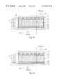
- FIG. 3presents the realization of a double-sided display element according to the invention using a liquid crystal display as an example.
- a liquid crystal displayAs an example, Starting in the center of the construction it is almost similar to the construction of a normal liquid crystal display, i.e. it has two glass plates 2 and 8 , between which there is at least liquid crystal 5 , more accurately construction 14 presented in FIG. 1 .
- the thickness of each glass plateis ca. 0.7 mm and the thickness of the liquid crystal between them is ca. 5 ⁇ m.
- Glass plates 2 , 8 and liquid crystal construction 14are common to both displays thus formed, i.e. to display D 1 having the viewing direction from up in the figure and to display D 2 having the viewing direction from below in the figure.
- first glass plate 2 ′For display D 1 the upper glass plate in the figure thus forms, seen from the viewing direction, first glass plate 2 ′ and the bottom glass plate forms second glass plate 8 ′.
- the bottom glass plate in the figurethus forms, seen from the viewing direction, first glass plate 2 ′′, and the upper glass plate forms second glass plate 8 ′′.
- the first layer of display D 1 counted in the viewing directionis first polarizer 1 ′, i.e. polarization filter 1 ′.
- first polarizer 1 ′i.e. polarization filter 1 ′.
- second polarizer 9 ′′i.e. polarization filter 9 ′′, and reflector 10 ′′ of display D 2 .
- First polarizer layer 1 ′ of display D 1 and second polarizer-reflector layer 9 ′′, 10 ′′(polarizer 9 ′′ and reflector 10 ′′ form one layer entity) are both ca. 0.3 to 0.35 mm thick.
- layers 1 ′ and 9 ′′, 10 ′′are separate pieces which are mounted/fixed next to each other on the same level (on the surface of a glass plate).
- the polarization levels of polarizers 1 and 9also depend on liquid crystal material 14 used.
- a twisted nematic (TN) liquid crystal displaythe polarization level of light twists as light passes through molecule layers, the direction of which is twisted.
- the polarization level of lighttwists 90° in liquid crystal layer 5 .
- the polarization filtersare often arranged in such a way that second polarizer 9 is at an 90° angle to first polarizer 1 , and hence a correct polarization level is obtained for the light which has passed liquid crystal layer 5 , hence all light (or a majority of the light) passes through second polarizer 9 .
- Reflector 10is preferably diffuse and maintains the polarization level, in which case the light passes back through second polarizer 9 , passes through liquid crystal layer 5 and passes through first polarizer 1 in the places in which there is no electric field between electrodes, in which case the display seems light, and correspondingly dark in the places where there is an electric field. If the liquid crystal layer twists the light for 270°, the polarizers are selected in such a way that the polarization level of second polarizer 9 is at an 270° angle to the polarization level of first polarizer 1 .
- Reasonably small (e.g. the ones used in Nokia 9000 Communicator) black/white displaysare often of the so called super twisted nematic (STN, Super Twisted Nematic) type, in which the twist angle usually is 270°.
- STNsuper twisted nematic
- first layer of display D 2is, when counted from the viewing direction, first polarizer 1 ′′, or polarization filter 1 ′′.
- display D 1 second polarizer 9 ′, or polarization filter 9 ′, and reflector 10 ′ of display D 1are 0.3-0.35 mm thick and they are equally in practice separate pieces which are placed/fixed next to each other on the same level on the surface of a glass plate. In this way a double sided display element is formed, by the use of which it is obtained smaller display D 1 (telephone part display) viewed from top in FIG. 3 and larger display D 2 (computer/organizer part display) viewed from downside, which thus are situated next to each other and they display information to opposite directions.
- the thickness of a display construction formed in this waywill be, using above dimensions, ca. 2.0 mm.
- electroluminescent background light layer 16 ′ and correspondingly 16 ′′it is possible to mount in displays D 1 and D 2 farthest in the viewing direction electroluminescent background light layer 16 ′ and correspondingly 16 ′′, if a background light is used and the construction of the background light is desired to be as thin as possible.
- the electroluminescent, or EL -background light layercan be formed out of laminated plastics, containing phosphorus between layers, which becomes illuminated when a voltage is connected over it.
- the voltage for the background light layercan be obtained from the display power supply or elsewhere in the device in which the display is mounted.
- An EL -background lightrequires high voltage (approximately 200 V) and thus normally requires a separate driver circuit.
- a display element according to the inventionis preferably not fixed to any circuit board, but driver circuits Dr of the display can be fixed directly on glass plate 2 ′′/ 8 ′′ of the display, using for example the chip-on-glass technique. This can be done in such a way that one longitudinal and one transverse edge of bottom glass plate 2 ′′/ 8 ′′ in the figure is slightly longer than the upper glass plate in the figure, hence on the edges of the bottom 2 ′′/ 8 ′′ glass plate there is room for mounting the driver circuits.
- Electrodes 3 and 7 of transparent conductive materialwhich have not been shown in detail in the figure, consist of transverse and longitudinal conductors, in the crossing points of which the pixels of the display form.
- the electrodesare controlled using driver circuits Dr, hence it is possible to make desired pixels light or dark and in such a way a desired figure can be formed in the display.
- driver circuits Drwhich control the whole display area of glass plates 2 and 8 using the longitudinal and transverse conductors, are capable of controlling the electrodes in the area of display D 1 and display D 2 .
- FIGS. 4 a and 4 bpresent a corresponding realization using plasma- or electroluminescence display.
- FIG. 4 apresents the structure of a plasma display for the realization of a display element according to the present invention.
- a plasma displaynormally has on top and in the bottom glass layers 32 and 38 .
- electrodes 33 and 37After the glass plates come electrodes 33 and 37 , of which the one closer to a viewer has usually been made transparent, for example by using indiumtinoxide (ITO). It has also been possible to use thin metal conductors because light emission spreads sideways in such a way that light is emitted. In a display element according to the invention both electrodes 33 and 37 are preferably realized using transparent conductors. Alternatively, it is possible to use a reversed construction in one part of the structure in such a way that for display D 1 electrodes 33 are made of a transparent material and electrodes 37 of metal, and for display D 2 electrodes 37 are made of a transparent material and electrodes 33 are made of metal.
- the electrodesare normally surrounded by an isolating layer 34 , 36 , between which there is gas layer 35 . Also in the ends of the gas layer there is isolating layer 39 , which can be of the same material as layers 34 and 36 (for example isolating solder-glass).
- isolating layer 39which can be of the same material as layers 34 and 36 (for example isolating solder-glass).
- the vertical dashed line in the figureillustrates the realization of two displays D 1 and D 2 displaying to two different directions.
- the display areascan be divided more clearly using suitable encapsulating, with which the other areas are covered, but apertures are left for the viewing of displays D 1 and D 2 .
- Longer glass plate 38 shown in the figureillustrates how, as in FIG. 3, by arranging one glass plate to be longer than the other one, driver circuits 31 can be placed on the edges using for example the chip-on-glass technique.
- FIG. 4 bpresents the structure of an electroluminescence display for the realization of a display element according to the present invention.
- An electroluminescence displaynormally has on top, closest to a viewer a glass layer and on the bottom a protective layer.
- Both topmost layer 42 and bottom layer 48 in an electroluminescence display according to the invention and in the figureare preferably glass plates.
- electrodes 43 and 47of which normally the one closer to a viewer has been made transparent, for example by using indiumtinoxide (ITO) and the second electrode has been made for example of aluminium.
- ITOindiumtinoxide
- both electrodes 43 and 47are preferably realized using transparent conductors.
- a reversed constructionis used in one part of the construction in such a way that for display D 1 electrodes 43 are made of a transparent material and electrodes 47 of aluminium or of some other metal, and for display D 2 electrodes 47 consist of a transparent material and electrodes 43 of aluminium or of some other metal.
- the electrodesare normally surrounded by an isolating layer 44 , 46 , for example of Y 2 O 3 , SiO 2 and Al 2 O 3 , between which there is electroluminescence film 45 , which can be formed of powder or using the thin film technique.
- Material 45is a semiconductor compound, usually for example ZnS with Mn as a compound blend.
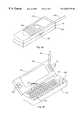
- FIGS. 5 a and 5 bpresent a telecommunication device utilizing a display element according to the invention, Nokia 9000 Communicator -terminal device, known as one, which is a multiservice mobile station with two sections.
- the inventionis also related to a terminal device comprising a two-way display element, which device can be made thinner compared with prior known devices.
- FIGS. 5 a and 5 bpresent an example of such a terminal device.
- a multiservice mobile stationcan be used in two different positions, the first of which shown in FIG. 5 a , the mobile telephone position, has been optimized for the using of the terminal device mainly like a conventional mobile telephone.
- the second position, the terminal device position shown in FIG. 5 bhas been optimized for the using of the terminal device as a versatile organizer and as a telecommunication terminal device.
- the terminal deviceis in FIG. 5 a shown in the mobile telephone position, when lid section 100 and base section 200 have been folded at a suitable angle against each other supported by hinge 190 (FIG. 5 b ).
- the top side of lid section 100comprises display 110 for displaying alphanumeric characters or graphic figures, i.e. display D 1 according to the invention, and keyboard 120 for entering alphanumeric characters in the terminal device.
- display 110has been arranged to display information connected with the telephone function, such as dialing a telephone number, the identification of an incoming call, and the scrolling of telephone function menus and other corresponding functions connected with a wireless telephone.
- Movable antenna 140is in a first embodiment according to the invention fixed to lid section 100 .
- FIG. 5 bthe terminal device is presented in the terminal device position, when lid section 100 and base section 200 have been folded in a suitable angle apart from each other supported by hinge 190 .
- the inside of lid section 100 and the top side of base section 200provide a user with an user interface comprising display 150 , i.e. display D 2 of a display element according to the invention, scroll keys 160 and command keys 170 , and base section 200 provides application keys 210 , QWERTY-keys 220 prior known from computers and cursor keys 230 .
- the display elementis fixed to the lid section for example alike in FIG. 3 to housing 17 .
Landscapes
- Physics & Mathematics (AREA)
- Nonlinear Science (AREA)
- General Physics & Mathematics (AREA)
- Chemical & Material Sciences (AREA)
- Crystallography & Structural Chemistry (AREA)
- Optics & Photonics (AREA)
- Mathematical Physics (AREA)
- Engineering & Computer Science (AREA)
- Theoretical Computer Science (AREA)
- Devices For Indicating Variable Information By Combining Individual Elements (AREA)
- Electric Clocks (AREA)
- Burglar Alarm Systems (AREA)
- Telephone Set Structure (AREA)
- Liquid Crystal (AREA)
- Gas-Filled Discharge Tubes (AREA)
Abstract
Description
Claims (22)
Priority Applications (1)
| Application Number | Priority Date | Filing Date | Title |
|---|---|---|---|
| US10/410,673US6747609B2 (en) | 1997-05-26 | 2003-04-09 | Dual display arrangement and a terminal device |
Applications Claiming Priority (2)
| Application Number | Priority Date | Filing Date | Title |
|---|---|---|---|
| FI972213AFI104658B (en) | 1997-05-26 | 1997-05-26 | Display arrangement and terminal with two displays |
| FI972213 | 1997-05-26 |
Related Child Applications (1)
| Application Number | Title | Priority Date | Filing Date |
|---|---|---|---|
| US10/410,673ContinuationUS6747609B2 (en) | 1997-05-26 | 2003-04-09 | Dual display arrangement and a terminal device |
Publications (1)
| Publication Number | Publication Date |
|---|---|
| US6583770B1true US6583770B1 (en) | 2003-06-24 |
Family
ID=8548907
Family Applications (2)
| Application Number | Title | Priority Date | Filing Date |
|---|---|---|---|
| US09/078,298Expired - LifetimeUS6583770B1 (en) | 1997-05-26 | 1998-05-13 | Dual display arrangement and a terminal device |
| US10/410,673Expired - LifetimeUS6747609B2 (en) | 1997-05-26 | 2003-04-09 | Dual display arrangement and a terminal device |
Family Applications After (1)
| Application Number | Title | Priority Date | Filing Date |
|---|---|---|---|
| US10/410,673Expired - LifetimeUS6747609B2 (en) | 1997-05-26 | 2003-04-09 | Dual display arrangement and a terminal device |
Country Status (8)
| Country | Link |
|---|---|
| US (2) | US6583770B1 (en) |
| EP (1) | EP0881617B1 (en) |
| JP (1) | JPH117259A (en) |
| KR (1) | KR100639314B1 (en) |
| CN (1) | CN1207694C (en) |
| AT (1) | ATE214507T1 (en) |
| DE (1) | DE69804156T2 (en) |
| FI (1) | FI104658B (en) |
Cited By (44)
| Publication number | Priority date | Publication date | Assignee | Title |
|---|---|---|---|---|
| US20030112390A1 (en)* | 2001-12-17 | 2003-06-19 | Nokia Corporation | Liquid crystal display |
| US20030189528A1 (en)* | 1997-05-26 | 2003-10-09 | Mika Antila | Dual display arrangement and a terminal device |
| US20040077385A1 (en)* | 2002-08-23 | 2004-04-22 | Sanyo Electric Co., Ltd. | Foldable electronic device |
| US20040080686A1 (en)* | 2002-10-25 | 2004-04-29 | Toppoly Optoelectronics Corp. | Dual-display liquid crystal display |
| US20040140947A1 (en)* | 2002-11-15 | 2004-07-22 | Takashi Tsuyuki | Display device |
| US20040183745A1 (en)* | 2003-03-20 | 2004-09-23 | Jeung-Hie Choi | Dual display apparatus |
| US20040201545A1 (en)* | 2003-04-09 | 2004-10-14 | Shunpei Yamazaki | Display device and an electronic apparatus using the same |
| US20040252076A1 (en)* | 2003-03-31 | 2004-12-16 | Yoshiyuki Kodama | Display device, electronic device and display method |
| US20040263056A1 (en)* | 2003-06-30 | 2004-12-30 | Satoshi Seo | Light-emitting device and electronic device |
| US20040263066A1 (en)* | 2003-04-07 | 2004-12-30 | Hiroko Abe | Electronic apparatus |
| US20050040753A1 (en)* | 2002-12-27 | 2005-02-24 | Mitsuaki Osame | Display device and electronic appliance |
| US20050057149A1 (en)* | 2003-09-03 | 2005-03-17 | Nokia Corporation | Method for manufacturing display; electronic device and display element |
| US20050091431A1 (en)* | 2003-10-23 | 2005-04-28 | Robert Olodort | Portable communication devices |
| US20050140565A1 (en)* | 2002-02-20 | 2005-06-30 | Rainer Krombach | Mobile telephone comprising wraparound display |
| US20050197165A1 (en)* | 2004-03-01 | 2005-09-08 | Hung-Chih Chen | Dual display module |
| US20050253789A1 (en)* | 2002-06-20 | 2005-11-17 | Hiroshi Ikeda | Display |
| US20060007165A1 (en)* | 2004-06-25 | 2006-01-12 | Kei-Hsiung Yang | Input-sensor-intergrated liquid crystal display panel |
| US20060066227A1 (en)* | 2004-09-24 | 2006-03-30 | Virnich James L | Electronic device with dual display arrangement |
| US20060125394A1 (en)* | 2004-12-14 | 2006-06-15 | Munisamy Anandan | Large area plasma display |
| US7089040B2 (en)* | 2000-01-27 | 2006-08-08 | Kyocera Corporation | Portable radio communication apparatus |
| US20060214880A1 (en)* | 2005-03-28 | 2006-09-28 | Moore Chad B | Double-sided fiber-based displays |
| US20070126654A1 (en)* | 2005-12-02 | 2007-06-07 | Samsung Electronics Co., Ltd. | Display device |
| US20070126962A1 (en)* | 2005-12-05 | 2007-06-07 | Semiconductor Energy Laboratory Co., Ltd. | Liquid crystal display device |
| US20070126670A1 (en)* | 2002-12-26 | 2007-06-07 | Semiconductor Energy Laboratory Co., Ltd. | Light Emitting Device and Electronic Appliance |
| US20070146580A1 (en)* | 2005-12-28 | 2007-06-28 | Semiconductor Energy Laboratory Co., Ltd. | Display device |
| CN1324361C (en)* | 2003-10-29 | 2007-07-04 | 铼宝科技股份有限公司 | Double-sided display device |
| US20070159044A1 (en)* | 2005-12-22 | 2007-07-12 | Semiconductor Energy Laboratory Co., Ltd. | Display device |
| US20070165008A1 (en)* | 2006-01-17 | 2007-07-19 | International Business Machines Corporation | Compact infrared touch screen apparatus |
| US20070177086A1 (en)* | 2006-02-02 | 2007-08-02 | Semiconductor Energy Laboratory Co., Ltd. | Display device |
| US20070177071A1 (en)* | 2006-01-31 | 2007-08-02 | Semiconductor Energy Laboratory Co., Ltd. | Display device |
| US20070200977A1 (en)* | 2006-02-24 | 2007-08-30 | Semiconductor Energy Laboratory Co., Ltd. | Display device |
| US20070200978A1 (en)* | 2006-02-24 | 2007-08-30 | Semiconductor Energy Laboratory Co., Ltd. | Display device |
| CN100335944C (en)* | 2003-10-29 | 2007-09-05 | 铼宝科技股份有限公司 | Double-sided display device |
| CN100442948C (en)* | 2005-03-02 | 2008-12-10 | 胜华科技股份有限公司 | Organic light emitting display capable of double-sided display |
| US20100198580A1 (en)* | 2000-10-25 | 2010-08-05 | Robert Glen Klinefelter | System, method, and apparatus for providing interpretive communication on a network |
| US20100214250A1 (en)* | 2001-05-16 | 2010-08-26 | Synaptics Incorporated | Touch screen with user interface enhancement |
| US20100277505A1 (en)* | 2009-04-30 | 2010-11-04 | Ludden Christopher A | Reduction in latency between user input and visual feedback |
| US20110037061A1 (en)* | 2003-04-02 | 2011-02-17 | Semiconductor Energy Laboratory Co., Ltd. | Light Emitting Device, Electronic Equipment and Apparatus For Manufacturing the Same |
| US20110148438A1 (en)* | 2009-12-18 | 2011-06-23 | Synaptics Incorporated | System and method for determining a number of objects in a capacitive sensing region using a shape factor |
| US20110148436A1 (en)* | 2009-12-18 | 2011-06-23 | Synaptics Incorporated | System and method for determining a number of objects in a capacitive sensing region using signal grouping |
| US20140002347A1 (en)* | 2012-06-27 | 2014-01-02 | Ga-Lane Chen | Touch panel with sapphire substrate and touch screen |
| US9642012B1 (en) | 2016-10-03 | 2017-05-02 | International Business Machines Corporation | Mobile device access control with two-layered display |
| US9852314B1 (en) | 2017-03-20 | 2017-12-26 | International Business Machines Corporation | Mobile device access control with two-layered display |
| US20210257861A1 (en)* | 2014-01-31 | 2021-08-19 | Semiconductor Energy Laboratory Co., Ltd. | Electronic device and its operation system |
Families Citing this family (65)
| Publication number | Priority date | Publication date | Assignee | Title |
|---|---|---|---|---|
| US7808694B2 (en)* | 1994-05-05 | 2010-10-05 | Qualcomm Mems Technologies, Inc. | Method and device for modulating light |
| US7852545B2 (en) | 1994-05-05 | 2010-12-14 | Qualcomm Mems Technologies, Inc. | Method and device for modulating light |
| US8928967B2 (en) | 1998-04-08 | 2015-01-06 | Qualcomm Mems Technologies, Inc. | Method and device for modulating light |
| WO1999052006A2 (en) | 1998-04-08 | 1999-10-14 | Etalon, Inc. | Interferometric modulation of radiation |
| KR20010000974A (en)* | 1998-11-02 | 2001-01-05 | 윤종용 | Both-sides liquid crystal display in cellular phone with folder type |
| AU2480600A (en)* | 1998-12-15 | 2000-07-03 | Qualcomm Incorporated | Dual view lcd assembly |
| GB9930449D0 (en)* | 1999-12-23 | 2000-02-16 | Promotion & Display Tech Ltd | Handset |
| JP2001186227A (en)* | 1999-12-27 | 2001-07-06 | Sanyo Electric Co Ltd | Folding type portable telephone set |
| US6574487B1 (en)* | 2000-02-23 | 2003-06-03 | Motorola, Inc. | Communication device with a dual-sided liquid crystal display |
| SE0000906L (en)* | 2000-03-20 | 2001-09-21 | Ericsson Telefon Ab L M | A portable communication device with a liquid crystal display and a way for its function. |
| KR20020040989A (en)* | 2000-11-25 | 2002-05-31 | 주식회사 현대 디스플레이 테크놀로지 | Backlight unit for irradiating to upper and lower |
| US7466961B1 (en)* | 2004-12-13 | 2008-12-16 | Palm, Inc. | Compact palmtop computer system and wireless telephone with foldable dual-sided display |
| KR20010035369A (en)* | 2001-02-07 | 2001-05-07 | 박종섭 | device for backright of dual polder handyphone |
| KR100762660B1 (en)* | 2001-03-09 | 2007-10-01 | 삼성전자주식회사 | Display device in folding portable wireless terminal |
| CN1462538A (en)* | 2001-04-27 | 2003-12-17 | 松下电器产业株式会社 | Portable information terminal device |
| US7142195B2 (en) | 2001-06-04 | 2006-11-28 | Palm, Inc. | Interface for interaction with display visible from both sides |
| JP2005504359A (en)* | 2001-09-28 | 2005-02-10 | コーニンクレッカ フィリップス エレクトロニクス エヌ ヴィ | Equipment with flat display |
| KR100424325B1 (en)* | 2001-11-07 | 2004-03-24 | 주식회사 어필텔레콤 | Dual LCD module of wireless phone |
| US6710754B2 (en)* | 2001-11-29 | 2004-03-23 | Palm, Inc. | Moveable output device |
| KR100454934B1 (en)* | 2001-12-10 | 2004-11-06 | 삼성전자주식회사 | Dual lcd mounting device of mobile phone |
| KR100440406B1 (en)* | 2001-12-14 | 2004-07-14 | 삼성전자주식회사 | Backlighting device for dual liquid crystal display and folder-type mobile phone therewith |
| US7034799B2 (en)* | 2001-12-14 | 2006-04-25 | Samsung Electronics Co., Ltd. | Backlighting device for dual liquid crystal display and folder-type mobile phone therewith |
| JP4141165B2 (en)* | 2002-04-09 | 2008-08-27 | 富士通株式会社 | Electronic equipment |
| US7237939B2 (en) | 2002-04-16 | 2007-07-03 | Samsung Electronics Co., Ltd. | Backlight assembly and liquid crystal display apparatus using the same |
| FI113130B (en)* | 2002-04-17 | 2004-02-27 | Nokia Corp | Portable, foldable electronic device equipped with telephone and camera functions |
| JP2004021238A (en)* | 2002-06-20 | 2004-01-22 | Nec Saitama Ltd | Display device and mobile terminal system |
| TWI266106B (en)* | 2002-08-09 | 2006-11-11 | Sanyo Electric Co | Display device with a plurality of display panels |
| JP4234376B2 (en)* | 2002-08-28 | 2009-03-04 | 東芝松下ディスプレイテクノロジー株式会社 | Display device and electronic device |
| US7230585B2 (en) | 2002-10-28 | 2007-06-12 | Sony Ericsson Mobile Communications Ab | Two-way displays and methods of operating the same |
| US7265383B2 (en) | 2002-12-13 | 2007-09-04 | Semiconductor Energy Laboratory Co., Ltd. | Light emitting device |
| KR100513105B1 (en) | 2003-03-27 | 2005-09-07 | 엘지.필립스 엘시디 주식회사 | Liquid Crystal Display Device |
| KR100539836B1 (en) | 2003-03-27 | 2005-12-28 | 엘지.필립스 엘시디 주식회사 | Liquid crystal display device |
| KR100518426B1 (en) | 2003-03-27 | 2005-09-29 | 엘지.필립스 엘시디 주식회사 | Liquid crystal display device |
| JP2004325600A (en)* | 2003-04-22 | 2004-11-18 | Semiconductor Energy Lab Co Ltd | Display device and electronic apparatus |
| WO2004104678A1 (en)* | 2003-05-21 | 2004-12-02 | Koninklijke Philips Electronics N.V. | Two-sided readable display device |
| US7161185B2 (en)* | 2003-06-27 | 2007-01-09 | Semiconductor Energy Laboratory Co., Ltd. | Display device and electronic device |
| US7453426B2 (en)* | 2004-01-14 | 2008-11-18 | Semiconductor Energy Laboratory Co., Ltd. | Display device and electronic apparatus |
| CN100378797C (en)* | 2004-03-05 | 2008-04-02 | 友达光电股份有限公司 | Double-screen display module |
| GB2413915B (en)* | 2004-05-04 | 2007-12-05 | Yogesh Kumar Kanhye | Mobile phone |
| US20060038752A1 (en)* | 2004-08-20 | 2006-02-23 | Eastman Kodak Company | Emission display |
| KR20080064902A (en)* | 2004-08-25 | 2008-07-09 | 문더기 테트놀로지스, 인크. | Wireless Digitizer Tablet and Digitizer Tablet Computer |
| EP1787976A4 (en)* | 2004-09-03 | 2008-08-13 | Asahi Kasei Chemicals Corp | PROCESS FOR MANUFACTURING LARGE PURITY DIARYLE CARBONATE WITH COMMERCIAL SCALE |
| US7545341B2 (en)* | 2005-02-18 | 2009-06-09 | Gfx International Inc. | Double-sided electronic display |
| TWI270025B (en)* | 2005-03-21 | 2007-01-01 | Au Optronics Corp | Dual emission display with integrated touch screen and fabricating method thereof |
| FI20055330A0 (en)* | 2005-06-20 | 2005-06-20 | Nokia Corp | Procedure, device and computer program product for checking an electronic device user interface |
| JP4926426B2 (en) | 2005-08-12 | 2012-05-09 | 株式会社半導体エネルギー研究所 | Electronics |
| JP4791165B2 (en)* | 2005-12-07 | 2011-10-12 | 富士フイルム株式会社 | camera |
| US7916980B2 (en) | 2006-01-13 | 2011-03-29 | Qualcomm Mems Technologies, Inc. | Interconnect structure for MEMS device |
| TWD118545S1 (en)* | 2006-03-27 | 2007-08-11 | 松下電器產業股份有限公司 | Portable Computer |
| US20070268201A1 (en)* | 2006-05-22 | 2007-11-22 | Sampsell Jeffrey B | Back-to-back displays |
| US7471442B2 (en)* | 2006-06-15 | 2008-12-30 | Qualcomm Mems Technologies, Inc. | Method and apparatus for low range bit depth enhancements for MEMS display architectures |
| KR101186530B1 (en)* | 2006-10-13 | 2012-10-08 | 엘지전자 주식회사 | Electronic device and controling method thereof |
| US7916378B2 (en) | 2007-03-08 | 2011-03-29 | Qualcomm Mems Technologies, Inc. | Method and apparatus for providing a light absorbing mask in an interferometric modulator display |
| US7847999B2 (en) | 2007-09-14 | 2010-12-07 | Qualcomm Mems Technologies, Inc. | Interferometric modulator display devices |
| US7944604B2 (en) | 2008-03-07 | 2011-05-17 | Qualcomm Mems Technologies, Inc. | Interferometric modulator in transmission mode |
| US7969638B2 (en) | 2008-04-10 | 2011-06-28 | Qualcomm Mems Technologies, Inc. | Device having thin black mask and method of fabricating the same |
| US7791783B2 (en)* | 2008-06-25 | 2010-09-07 | Qualcomm Mems Technologies, Inc. | Backlight displays |
| JP2012083659A (en)* | 2010-10-14 | 2012-04-26 | Nsc:Kk | Method for manufacturing glass substrate for electronic device |
| US8599158B2 (en) | 2011-06-29 | 2013-12-03 | Nokia Corporation | Multi-surface touch sensitive apparatus and method |
| WO2013107474A1 (en)* | 2012-01-20 | 2013-07-25 | Sony Ericsson Mobile Communications Ab | Touch screen, portable electronic device, and method of operating a touch screen |
| CN105355646B (en)* | 2015-11-13 | 2019-03-22 | 京东方科技集团股份有限公司 | Array substrate and preparation method thereof, display device |
| CN105951080B (en)* | 2016-06-27 | 2018-11-20 | 力同铝业(广东)有限公司 | Aluminum alloy surface composite passivant and preparation method thereof |
| JP6950742B2 (en)* | 2017-10-04 | 2021-10-13 | Agc株式会社 | Display and television equipment |
| JP2020118924A (en)* | 2019-01-28 | 2020-08-06 | セイコーエプソン株式会社 | Electro-optical device, display control system, display driver, electronic device and moving body |
| CN213399371U (en)* | 2020-11-20 | 2021-06-08 | 福建天泉教育科技有限公司 | Double-screen tablet personal computer for students |
Citations (29)
| Publication number | Priority date | Publication date | Assignee | Title |
|---|---|---|---|---|
| GB2074356A (en) | 1980-04-16 | 1981-10-28 | Asulab Sa | Passive Electro-Optic Display Cell |
| US4611897A (en)* | 1984-06-05 | 1986-09-16 | Nippon Kogaku K. K. | Segment indication device |
| US4720781A (en)* | 1983-11-30 | 1988-01-19 | Stc Plc | Data processing terminal having support module and portable display module for liquid crystal display |
| US4794390A (en)* | 1986-03-10 | 1988-12-27 | Lippman Jeffrey H | Alphanumeric display means |
| US5016002A (en) | 1988-04-15 | 1991-05-14 | Nokia-Mobira Oy | Matrix display |
| US5049862A (en)* | 1989-10-06 | 1991-09-17 | Communication Intelligence Corporation ("Cic") | Keyless flat panel portable computer--computer aided notebook |
| US5189632A (en)* | 1990-08-20 | 1993-02-23 | Oy Nokia Ab | Portable personal computer and mobile telephone device |
| US5337346A (en)* | 1991-09-26 | 1994-08-09 | Casio Computer Co., Ltd. | Portable telephone apparatus including electronic notebook function |
| US5467102A (en)* | 1992-08-31 | 1995-11-14 | Kabushiki Kaisha Toshiba | Portable display device with at least two display screens controllable collectively or separately |
| US5584054A (en)* | 1994-07-18 | 1996-12-10 | Motorola, Inc. | Communication device having a movable front cover for exposing a touch sensitive display |
| GB2305532A (en) | 1995-09-26 | 1997-04-09 | Samsung Display Devices Co Ltd | Liquid crystal display |
| US5653522A (en)* | 1993-08-25 | 1997-08-05 | Kopin Corporation | Display panel mount for projection dislay system |
| US5657370A (en)* | 1994-05-18 | 1997-08-12 | Nec Corporation | Cellular portable radiotelephone |
| US5687939A (en)* | 1996-04-26 | 1997-11-18 | Moscovitch; Jerry | Dual display system |
| US5706068A (en)* | 1993-12-15 | 1998-01-06 | Ois Optical Imaging Systems, Inc. | Method of making and using a normally white twisted nematic LCD with negative retardation film on each side of liquid crystal |
| US5742894A (en)* | 1995-02-06 | 1998-04-21 | Motorola, Inc. | Radio communication device having a moveable housing element and keypad disposed therein |
| US5835458A (en)* | 1994-09-09 | 1998-11-10 | Gemfire Corporation | Solid state optical data reader using an electric field for routing control |
| US5854997A (en)* | 1994-09-07 | 1998-12-29 | Hitachi, Ltd. | Electronic interpreter utilizing linked sets of sentences |
| US5859623A (en)* | 1996-05-14 | 1999-01-12 | Proxima Corporation | Intelligent display system presentation projection arrangement and method of using same |
| US5896575A (en)* | 1997-02-28 | 1999-04-20 | Motorola, Inc. | Electronic device with display viewable from two opposite ends |
| US5929834A (en)* | 1995-04-25 | 1999-07-27 | Brinks Hofer Gilson & Lione | Liquid crystal display device with tablet |
| US5949643A (en)* | 1996-11-18 | 1999-09-07 | Batio; Jeffry | Portable computer having split keyboard and pivotal display screen halves |
| US5977934A (en)* | 1995-10-19 | 1999-11-02 | Hitachi, Ltd. | Information processing apparatus |
| US5995175A (en)* | 1993-03-04 | 1999-11-30 | Samsung Electronics Co., Ltd. | Liquid crystal display and a method for manufacturing the same |
| US6014573A (en)* | 1995-11-24 | 2000-01-11 | Nokia Mobile Phones, Ltd. | Function for facilitating use of a double-acting communication device and a double-acting communication device |
| US6047196A (en)* | 1995-11-24 | 2000-04-04 | Nokia Mobile Phones, Ltd. | Communication device with two modes of operation |
| US6073034A (en)* | 1996-10-31 | 2000-06-06 | Kopin Corporation | Wireless telephone display system |
| US6144358A (en)* | 1997-08-20 | 2000-11-07 | Lucent Technologies Inc. | Multi-display electronic devices having open and closed configurations |
| US6327482B1 (en)* | 1998-05-28 | 2001-12-04 | Nec Corporation | Mobile radio apparatus with auxiliary display screen |
Family Cites Families (5)
| Publication number | Priority date | Publication date | Assignee | Title |
|---|---|---|---|---|
| JPS6231530A (en)* | 1985-08-02 | 1987-02-10 | Ricoh Co Ltd | Automotive display device |
| FR2701586B1 (en)* | 1993-02-12 | 1995-03-24 | Souriau Diagnostic Electron | Liquid crystal display device comprising an array of image points. |
| GB9316961D0 (en)* | 1993-08-14 | 1994-01-26 | Marconi Gec Ltd | Display arrangements |
| KR970022945A (en)* | 1995-10-09 | 1997-05-30 | 구자홍 | Dual display device of portable personal digital assistant |
| FI104658B (en)* | 1997-05-26 | 2000-03-15 | Nokia Mobile Phones Ltd | Display arrangement and terminal with two displays |
- 1997
- 1997-05-26FIFI972213Apatent/FI104658B/ennot_activeIP Right Cessation
- 1998
- 1998-05-04DEDE69804156Tpatent/DE69804156T2/ennot_activeExpired - Lifetime
- 1998-05-04EPEP98660039Apatent/EP0881617B1/ennot_activeExpired - Lifetime
- 1998-05-04ATAT98660039Tpatent/ATE214507T1/enactive
- 1998-05-13USUS09/078,298patent/US6583770B1/ennot_activeExpired - Lifetime
- 1998-05-25KRKR1019980018813Apatent/KR100639314B1/ennot_activeExpired - Fee Related
- 1998-05-25JPJP10142931Apatent/JPH117259A/enactivePending
- 1998-05-26CNCNB981089755Apatent/CN1207694C/ennot_activeExpired - Fee Related
- 2003
- 2003-04-09USUS10/410,673patent/US6747609B2/ennot_activeExpired - Lifetime
Patent Citations (29)
| Publication number | Priority date | Publication date | Assignee | Title |
|---|---|---|---|---|
| GB2074356A (en) | 1980-04-16 | 1981-10-28 | Asulab Sa | Passive Electro-Optic Display Cell |
| US4720781A (en)* | 1983-11-30 | 1988-01-19 | Stc Plc | Data processing terminal having support module and portable display module for liquid crystal display |
| US4611897A (en)* | 1984-06-05 | 1986-09-16 | Nippon Kogaku K. K. | Segment indication device |
| US4794390A (en)* | 1986-03-10 | 1988-12-27 | Lippman Jeffrey H | Alphanumeric display means |
| US5016002A (en) | 1988-04-15 | 1991-05-14 | Nokia-Mobira Oy | Matrix display |
| US5049862A (en)* | 1989-10-06 | 1991-09-17 | Communication Intelligence Corporation ("Cic") | Keyless flat panel portable computer--computer aided notebook |
| US5189632A (en)* | 1990-08-20 | 1993-02-23 | Oy Nokia Ab | Portable personal computer and mobile telephone device |
| US5337346A (en)* | 1991-09-26 | 1994-08-09 | Casio Computer Co., Ltd. | Portable telephone apparatus including electronic notebook function |
| US5467102A (en)* | 1992-08-31 | 1995-11-14 | Kabushiki Kaisha Toshiba | Portable display device with at least two display screens controllable collectively or separately |
| US5995175A (en)* | 1993-03-04 | 1999-11-30 | Samsung Electronics Co., Ltd. | Liquid crystal display and a method for manufacturing the same |
| US5653522A (en)* | 1993-08-25 | 1997-08-05 | Kopin Corporation | Display panel mount for projection dislay system |
| US5706068A (en)* | 1993-12-15 | 1998-01-06 | Ois Optical Imaging Systems, Inc. | Method of making and using a normally white twisted nematic LCD with negative retardation film on each side of liquid crystal |
| US5657370A (en)* | 1994-05-18 | 1997-08-12 | Nec Corporation | Cellular portable radiotelephone |
| US5584054A (en)* | 1994-07-18 | 1996-12-10 | Motorola, Inc. | Communication device having a movable front cover for exposing a touch sensitive display |
| US5854997A (en)* | 1994-09-07 | 1998-12-29 | Hitachi, Ltd. | Electronic interpreter utilizing linked sets of sentences |
| US5835458A (en)* | 1994-09-09 | 1998-11-10 | Gemfire Corporation | Solid state optical data reader using an electric field for routing control |
| US5742894A (en)* | 1995-02-06 | 1998-04-21 | Motorola, Inc. | Radio communication device having a moveable housing element and keypad disposed therein |
| US5929834A (en)* | 1995-04-25 | 1999-07-27 | Brinks Hofer Gilson & Lione | Liquid crystal display device with tablet |
| GB2305532A (en) | 1995-09-26 | 1997-04-09 | Samsung Display Devices Co Ltd | Liquid crystal display |
| US5977934A (en)* | 1995-10-19 | 1999-11-02 | Hitachi, Ltd. | Information processing apparatus |
| US6014573A (en)* | 1995-11-24 | 2000-01-11 | Nokia Mobile Phones, Ltd. | Function for facilitating use of a double-acting communication device and a double-acting communication device |
| US6047196A (en)* | 1995-11-24 | 2000-04-04 | Nokia Mobile Phones, Ltd. | Communication device with two modes of operation |
| US5687939A (en)* | 1996-04-26 | 1997-11-18 | Moscovitch; Jerry | Dual display system |
| US5859623A (en)* | 1996-05-14 | 1999-01-12 | Proxima Corporation | Intelligent display system presentation projection arrangement and method of using same |
| US6073034A (en)* | 1996-10-31 | 2000-06-06 | Kopin Corporation | Wireless telephone display system |
| US5949643A (en)* | 1996-11-18 | 1999-09-07 | Batio; Jeffry | Portable computer having split keyboard and pivotal display screen halves |
| US5896575A (en)* | 1997-02-28 | 1999-04-20 | Motorola, Inc. | Electronic device with display viewable from two opposite ends |
| US6144358A (en)* | 1997-08-20 | 2000-11-07 | Lucent Technologies Inc. | Multi-display electronic devices having open and closed configurations |
| US6327482B1 (en)* | 1998-05-28 | 2001-12-04 | Nec Corporation | Mobile radio apparatus with auxiliary display screen |
Cited By (88)
| Publication number | Priority date | Publication date | Assignee | Title |
|---|---|---|---|---|
| US20030189528A1 (en)* | 1997-05-26 | 2003-10-09 | Mika Antila | Dual display arrangement and a terminal device |
| US6747609B2 (en)* | 1997-05-26 | 2004-06-08 | Nokia Mobile Phones, Ltd. | Dual display arrangement and a terminal device |
| US7089040B2 (en)* | 2000-01-27 | 2006-08-08 | Kyocera Corporation | Portable radio communication apparatus |
| US20100198580A1 (en)* | 2000-10-25 | 2010-08-05 | Robert Glen Klinefelter | System, method, and apparatus for providing interpretive communication on a network |
| US10499168B2 (en)* | 2000-10-25 | 2019-12-03 | Kp Innovations, Llc | System, method, and apparatus for providing interpretive communication on a network |
| US8560947B2 (en) | 2001-05-16 | 2013-10-15 | Synaptics Incorporated | Touch screen with user interface enhancement |
| US20100214250A1 (en)* | 2001-05-16 | 2010-08-26 | Synaptics Incorporated | Touch screen with user interface enhancement |
| US20100275033A1 (en)* | 2001-05-16 | 2010-10-28 | Synaptics Incorporated | Touch screen with user interface enhancement |
| US8402372B2 (en)* | 2001-05-16 | 2013-03-19 | Synaptics Incorporated | Touch screen with user interface enhancement |
| US20030112390A1 (en)* | 2001-12-17 | 2003-06-19 | Nokia Corporation | Liquid crystal display |
| US6812973B2 (en)* | 2001-12-17 | 2004-11-02 | Nokia Corporation | Liquid crystal display having movable reflector surfaces providing sub-displays viewable from different viewing directions |
| US20050140565A1 (en)* | 2002-02-20 | 2005-06-30 | Rainer Krombach | Mobile telephone comprising wraparound display |
| US20050253789A1 (en)* | 2002-06-20 | 2005-11-17 | Hiroshi Ikeda | Display |
| US7567823B2 (en)* | 2002-08-23 | 2009-07-28 | Kyocera Corporation | Foldable electronic device |
| US20040077385A1 (en)* | 2002-08-23 | 2004-04-22 | Sanyo Electric Co., Ltd. | Foldable electronic device |
| US6791643B2 (en)* | 2002-10-25 | 2004-09-14 | Toppoly Optoelectronics Corp. | Dual-display liquid crystal display |
| US20040080686A1 (en)* | 2002-10-25 | 2004-04-29 | Toppoly Optoelectronics Corp. | Dual-display liquid crystal display |
| US20040140947A1 (en)* | 2002-11-15 | 2004-07-22 | Takashi Tsuyuki | Display device |
| US20080150870A1 (en)* | 2002-11-15 | 2008-06-26 | Takashi Tsuyuki | Display Device |
| US7336252B2 (en)* | 2002-11-15 | 2008-02-26 | Hitachi Displays, Ltd. | Display device |
| US7956835B2 (en) | 2002-11-15 | 2011-06-07 | Hitachi Displays, Ltd. | Display device |
| US7808457B2 (en) | 2002-12-26 | 2010-10-05 | Semiconductor Energy Laboratory Co., Ltd. | Light emitting device and electronic appliance |
| US20070126670A1 (en)* | 2002-12-26 | 2007-06-07 | Semiconductor Energy Laboratory Co., Ltd. | Light Emitting Device and Electronic Appliance |
| US20050040753A1 (en)* | 2002-12-27 | 2005-02-24 | Mitsuaki Osame | Display device and electronic appliance |
| US7355338B2 (en)* | 2002-12-27 | 2008-04-08 | Semiconductor Energy Laboratory Co., Ltd. | Electronic device provided with multiple display panels including at least one dual electroluminescent light emission panel |
| US20040183745A1 (en)* | 2003-03-20 | 2004-09-23 | Jeung-Hie Choi | Dual display apparatus |
| US20040252076A1 (en)* | 2003-03-31 | 2004-12-16 | Yoshiyuki Kodama | Display device, electronic device and display method |
| US20110037061A1 (en)* | 2003-04-02 | 2011-02-17 | Semiconductor Energy Laboratory Co., Ltd. | Light Emitting Device, Electronic Equipment and Apparatus For Manufacturing the Same |
| US8912712B2 (en) | 2003-04-02 | 2014-12-16 | Semiconductor Energy Laboratory Co., Ltd. | Light emitting device, electronic equipment and apparatus for manufacturing the same |
| US20040263066A1 (en)* | 2003-04-07 | 2004-12-30 | Hiroko Abe | Electronic apparatus |
| US20090179549A1 (en)* | 2003-04-07 | 2009-07-16 | Semiconductor Energy Laboratory Co., Ltd. | Electronic display including a light-emitting element and a color filter sandwiched between two polarizers |
| US8242683B2 (en) | 2003-04-07 | 2012-08-14 | Semiconductor Energy Laboratory Co., Ltd. | Electronic display including a light-emitting element and a color filter sandwiched between two polarizers |
| US8009145B2 (en) | 2003-04-09 | 2011-08-30 | Semiconductor Energy Laboratory Co., Ltd. | Display device and an electronic apparatus using the same |
| US20040201545A1 (en)* | 2003-04-09 | 2004-10-14 | Shunpei Yamazaki | Display device and an electronic apparatus using the same |
| US8330670B2 (en) | 2003-04-09 | 2012-12-11 | Semiconductor Energy Laboratory Co., Ltd. | Display device and an electronic apparatus using the same |
| US7327335B2 (en)* | 2003-04-09 | 2008-02-05 | Semiconductor Energy Laboratory Co., Ltd. | Display device and an electronic apparatus using the same |
| US8760375B2 (en) | 2003-04-09 | 2014-06-24 | Semiconductor Energy Laboratory Co., Ltd. | Display device and an electronic apparatus using the same |
| US7622863B2 (en) | 2003-06-30 | 2009-11-24 | Semiconductor Energy Laboratory Co., Ltd. | Light-emitting device and electronic device including first and second light emitting elements |
| US20040263056A1 (en)* | 2003-06-30 | 2004-12-30 | Satoshi Seo | Light-emitting device and electronic device |
| US20050057149A1 (en)* | 2003-09-03 | 2005-03-17 | Nokia Corporation | Method for manufacturing display; electronic device and display element |
| US20050091431A1 (en)* | 2003-10-23 | 2005-04-28 | Robert Olodort | Portable communication devices |
| CN1324361C (en)* | 2003-10-29 | 2007-07-04 | 铼宝科技股份有限公司 | Double-sided display device |
| CN100335944C (en)* | 2003-10-29 | 2007-09-05 | 铼宝科技股份有限公司 | Double-sided display device |
| US7406338B2 (en)* | 2004-03-01 | 2008-07-29 | Au Optronics Corporation | Dual display module |
| US20050197165A1 (en)* | 2004-03-01 | 2005-09-08 | Hung-Chih Chen | Dual display module |
| US20060007165A1 (en)* | 2004-06-25 | 2006-01-12 | Kei-Hsiung Yang | Input-sensor-intergrated liquid crystal display panel |
| US20060066227A1 (en)* | 2004-09-24 | 2006-03-30 | Virnich James L | Electronic device with dual display arrangement |
| US7498743B2 (en)* | 2004-12-14 | 2009-03-03 | Munisamy Anandan | Large area plasma display with increased discharge path |
| US20060125394A1 (en)* | 2004-12-14 | 2006-06-15 | Munisamy Anandan | Large area plasma display |
| CN100442948C (en)* | 2005-03-02 | 2008-12-10 | 胜华科技股份有限公司 | Organic light emitting display capable of double-sided display |
| US7656365B2 (en)* | 2005-03-28 | 2010-02-02 | Chad Byron Moore | Double-sided fiber-based displays |
| US20060214880A1 (en)* | 2005-03-28 | 2006-09-28 | Moore Chad B | Double-sided fiber-based displays |
| US20070126654A1 (en)* | 2005-12-02 | 2007-06-07 | Samsung Electronics Co., Ltd. | Display device |
| US20070126962A1 (en)* | 2005-12-05 | 2007-06-07 | Semiconductor Energy Laboratory Co., Ltd. | Liquid crystal display device |
| US7808164B2 (en) | 2005-12-22 | 2010-10-05 | Semiconductor Energy Laboratory Co., Ltd. | Display device |
| US20070159044A1 (en)* | 2005-12-22 | 2007-07-12 | Semiconductor Energy Laboratory Co., Ltd. | Display device |
| US7804560B2 (en) | 2005-12-28 | 2010-09-28 | Semiconductor Energy Laboratory Co., Ltd. | Display device |
| US20070146580A1 (en)* | 2005-12-28 | 2007-06-28 | Semiconductor Energy Laboratory Co., Ltd. | Display device |
| US20070165008A1 (en)* | 2006-01-17 | 2007-07-19 | International Business Machines Corporation | Compact infrared touch screen apparatus |
| US20110051034A1 (en)* | 2006-01-31 | 2011-03-03 | Semiconductor Energy Laboratory Co., Ltd. | Display Device |
| US20100245712A1 (en)* | 2006-01-31 | 2010-09-30 | Semiconductor Energy Laboratory Co., Ltd. | Liquid crystal DISPLAY DEVICE having a pair of electrodes over an inner side of a substrate of a liquid crystal element in which a stack of polarizers on the outer side of a substrate are provided and arranged between a pair of protective layers such that no protective layer is located between the stacked polarizers |
| US9164313B2 (en) | 2006-01-31 | 2015-10-20 | Semiconductor Energy Laboratory Co., Ltd. | Display device |
| US20070177071A1 (en)* | 2006-01-31 | 2007-08-02 | Semiconductor Energy Laboratory Co., Ltd. | Display device |
| US7738055B2 (en) | 2006-01-31 | 2010-06-15 | Semiconductor Energy Laboratory Co., Ltd. | Display device having stacked polarizers that differ in degrees of light absorbing bands and that are between a pair of protective layers such that no protective layer is located between the stacked polarizers |
| US7855770B2 (en) | 2006-01-31 | 2010-12-21 | Semiconductor Energy Laboratory Co., Ltd. | Liquid crystal display device having a pair of electrodes over an inner side of a substrate of a liquid crystal element in which a stack of polarizers on the outer side of a substrate are provided and arranged between a pair of protective layers such that no protective layer is located between the stacked polarizers |
| US20070177086A1 (en)* | 2006-02-02 | 2007-08-02 | Semiconductor Energy Laboratory Co., Ltd. | Display device |
| US8610846B2 (en) | 2006-02-02 | 2013-12-17 | Semiconductor Energy Laboratory Co., Ltd. | Display device with stacked polarizers |
| US8405800B2 (en) | 2006-02-02 | 2013-03-26 | Semiconductor Energy Laboratory Co., Ltd. | Display device with stacked polarizers |
| US8670091B2 (en) | 2006-02-24 | 2014-03-11 | Semiconductor Energy Laboratory Co., Ltd. | Display device having stack of polarizers with wavelength distribution of extinction coefficient |
| US20070200977A1 (en)* | 2006-02-24 | 2007-08-30 | Semiconductor Energy Laboratory Co., Ltd. | Display device |
| US20070200978A1 (en)* | 2006-02-24 | 2007-08-30 | Semiconductor Energy Laboratory Co., Ltd. | Display device |
| US20110063545A1 (en)* | 2006-02-24 | 2011-03-17 | Semiconductor Energy Laboratory Co., Ltd. | Display device |
| US7956957B2 (en) | 2006-02-24 | 2011-06-07 | Semiconductor Energy Laboratory Co., Ltd. | Display device |
| US7864268B2 (en) | 2006-02-24 | 2011-01-04 | Semiconductor Energy Laboratory Co., Ltd. | Display device with stack of polarizers having wavelength distributions of extinction coefficient of absorption axes |
| US10254878B2 (en) | 2009-04-30 | 2019-04-09 | Synaptics Incorporated | Operating a touch screen control system according to a plurality of rule sets |
| US20100277505A1 (en)* | 2009-04-30 | 2010-11-04 | Ludden Christopher A | Reduction in latency between user input and visual feedback |
| US8564555B2 (en) | 2009-04-30 | 2013-10-22 | Synaptics Incorporated | Operating a touch screen control system according to a plurality of rule sets |
| US9052764B2 (en) | 2009-04-30 | 2015-06-09 | Synaptics Incorporated | Operating a touch screen control system according to a plurality of rule sets |
| US9304619B2 (en) | 2009-04-30 | 2016-04-05 | Synaptics Incorporated | Operating a touch screen control system according to a plurality of rule sets |
| US20100277429A1 (en)* | 2009-04-30 | 2010-11-04 | Day Shawn P | Operating a touch screen control system according to a plurality of rule sets |
| US9703411B2 (en) | 2009-04-30 | 2017-07-11 | Synaptics Incorporated | Reduction in latency between user input and visual feedback |
| US20110148438A1 (en)* | 2009-12-18 | 2011-06-23 | Synaptics Incorporated | System and method for determining a number of objects in a capacitive sensing region using a shape factor |
| US20110148436A1 (en)* | 2009-12-18 | 2011-06-23 | Synaptics Incorporated | System and method for determining a number of objects in a capacitive sensing region using signal grouping |
| US20140002347A1 (en)* | 2012-06-27 | 2014-01-02 | Ga-Lane Chen | Touch panel with sapphire substrate and touch screen |
| US20210257861A1 (en)* | 2014-01-31 | 2021-08-19 | Semiconductor Energy Laboratory Co., Ltd. | Electronic device and its operation system |
| US12271241B2 (en)* | 2014-01-31 | 2025-04-08 | Semiconductor Energy Laboratory Co., Ltd. | Electronic device including two batteries and two display panels |
| US9642012B1 (en) | 2016-10-03 | 2017-05-02 | International Business Machines Corporation | Mobile device access control with two-layered display |
| US9852314B1 (en) | 2017-03-20 | 2017-12-26 | International Business Machines Corporation | Mobile device access control with two-layered display |
Also Published As
| Publication number | Publication date |
|---|---|
| CN1200526A (en) | 1998-12-02 |
| EP0881617B1 (en) | 2002-03-13 |
| FI972213A0 (en) | 1997-05-26 |
| EP0881617A1 (en) | 1998-12-02 |
| DE69804156D1 (en) | 2002-04-18 |
| US20030189528A1 (en) | 2003-10-09 |
| JPH117259A (en) | 1999-01-12 |
| KR100639314B1 (en) | 2006-12-22 |
| US6747609B2 (en) | 2004-06-08 |
| DE69804156T2 (en) | 2002-10-31 |
| FI104658B (en) | 2000-03-15 |
| KR19980087342A (en) | 1998-12-05 |
| ATE214507T1 (en) | 2002-03-15 |
| FI972213L (en) | 1998-11-27 |
| CN1207694C (en) | 2005-06-22 |
Similar Documents
| Publication | Publication Date | Title |
|---|---|---|
| US6583770B1 (en) | Dual display arrangement and a terminal device | |
| US6839109B2 (en) | Liquid crystal display with display regions of light reflection mode and light transmission mode | |
| US6842170B1 (en) | Display with aligned optical shutter and backlight cells applicable for use with a touchscreen | |
| US6961105B2 (en) | Dual-display module with a tunable mirror sheet | |
| US6958796B2 (en) | Substrate for electro-optical device, electro-optical device and electronic apparatus | |
| WO2000036578A1 (en) | Dual view lcd assembly | |
| EP1791019B1 (en) | Display apparatus | |
| WO2004093332A2 (en) | Automatic background color change of monochrome liquid crystal display | |
| US20090058783A1 (en) | Liquid crystal display device | |
| CN101142514A (en) | Liquid crystal display device and mobile terminal device | |
| EP1918764A1 (en) | Multi-panel display apparatus | |
| EP1182494B1 (en) | Liquid crystal panel | |
| US7148940B2 (en) | Reflective liquid crystal display for dual display | |
| KR20080084334A (en) | LCD Display Module | |
| JP4178870B2 (en) | Electro-optical panel, electro-optical device and electronic apparatus | |
| CN107463032B (en) | Liquid crystal display panel and display device | |
| JP4202652B2 (en) | Liquid crystal display device and portable information terminal | |
| JP4114336B2 (en) | Color filter substrate, method for manufacturing color filter substrate, liquid crystal display panel, liquid crystal display device, and electronic apparatus | |
| JPH11119206A (en) | Reflection type color liquid crystal display device and its production | |
| JP2003248444A (en) | Electro-optical device substrate, electro-optical device and electronic equipment | |
| KR100349916B1 (en) | Portable display device | |
| KR20010077355A (en) | Forder type plat display device | |
| KR20070037112A (en) | Back light unit and liquid crystal display device having same |
Legal Events
| Date | Code | Title | Description |
|---|---|---|---|
| AS | Assignment | Owner name:NOKIA MOBILE PHONES LTD., FINLAND Free format text:ASSIGNMENT OF ASSIGNORS INTEREST;ASSIGNORS:ANTILA, MIKA;RONKKA, RISTO;REEL/FRAME:009176/0296 Effective date:19980429 | |
| STCF | Information on status: patent grant | Free format text:PATENTED CASE | |
| FPAY | Fee payment | Year of fee payment:4 | |
| FEPP | Fee payment procedure | Free format text:PAYOR NUMBER ASSIGNED (ORIGINAL EVENT CODE: ASPN); ENTITY STATUS OF PATENT OWNER: LARGE ENTITY | |
| FPAY | Fee payment | Year of fee payment:8 | |
| FPAY | Fee payment | Year of fee payment:12 | |
| AS | Assignment | Owner name:NOKIA TECHNOLOGIES OY, FINLAND Free format text:ASSIGNMENT OF ASSIGNORS INTEREST;ASSIGNOR:NOKIA CORPORATION;REEL/FRAME:036067/0222 Effective date:20150116 | |
| AS | Assignment | Owner name:OMEGA CREDIT OPPORTUNITIES MASTER FUND, LP, NEW YORK Free format text:SECURITY INTEREST;ASSIGNOR:WSOU INVESTMENTS, LLC;REEL/FRAME:043966/0574 Effective date:20170822 Owner name:OMEGA CREDIT OPPORTUNITIES MASTER FUND, LP, NEW YO Free format text:SECURITY INTEREST;ASSIGNOR:WSOU INVESTMENTS, LLC;REEL/FRAME:043966/0574 Effective date:20170822 | |
| AS | Assignment | Owner name:WSOU INVESTMENTS, LLC, CALIFORNIA Free format text:ASSIGNMENT OF ASSIGNORS INTEREST;ASSIGNOR:NOKIA TECHNOLOGIES OY;REEL/FRAME:043953/0822 Effective date:20170722 | |
| AS | Assignment | Owner name:WSOU INVESTMENTS, LLC, CALIFORNIA Free format text:RELEASE BY SECURED PARTY;ASSIGNOR:OCO OPPORTUNITIES MASTER FUND, L.P. (F/K/A OMEGA CREDIT OPPORTUNITIES MASTER FUND LP;REEL/FRAME:049246/0405 Effective date:20190516 |