US6583469B1 - Self-aligned dog-bone structure for FinFET applications and methods to fabricate the same - Google Patents
Self-aligned dog-bone structure for FinFET applications and methods to fabricate the sameDownload PDFInfo
- Publication number
- US6583469B1 US6583469B1US09/683,626US68362602AUS6583469B1US 6583469 B1US6583469 B1US 6583469B1US 68362602 AUS68362602 AUS 68362602AUS 6583469 B1US6583469 B1US 6583469B1
- Authority
- US
- United States
- Prior art keywords
- region
- source
- horizontal width
- vertically oriented
- channel region
- Prior art date
- Legal status (The legal status is an assumption and is not a legal conclusion. Google has not performed a legal analysis and makes no representation as to the accuracy of the status listed.)
- Expired - Lifetime
Links
- 238000000034methodMethods0.000titleabstractdescription40
- 239000004065semiconductorSubstances0.000claimsdescription31
- 150000004767nitridesChemical class0.000claimsdescription24
- 239000000758substrateSubstances0.000claimsdescription5
- 230000005669field effectEffects0.000claimsdescription3
- 229910021332silicideInorganic materials0.000claimsdescription3
- FVBUAEGBCNSCDD-UHFFFAOYSA-Nsilicide(4-)Chemical compound[Si-4]FVBUAEGBCNSCDD-UHFFFAOYSA-N0.000claimsdescription3
- 238000005530etchingMethods0.000description46
- 229920002120photoresistant polymerPolymers0.000description17
- 239000011810insulating materialSubstances0.000description12
- 210000000746body regionAnatomy0.000description11
- 239000000463materialSubstances0.000description11
- VYPSYNLAJGMNEJ-UHFFFAOYSA-NSilicium dioxideChemical compoundO=[Si]=OVYPSYNLAJGMNEJ-UHFFFAOYSA-N0.000description8
- 125000006850spacer groupChemical group0.000description8
- 238000005137deposition processMethods0.000description7
- 238000005229chemical vapour depositionMethods0.000description6
- 238000000151depositionMethods0.000description6
- 230000008021depositionEffects0.000description6
- 230000000694effectsEffects0.000description6
- 239000012212insulatorSubstances0.000description6
- 230000003647oxidationEffects0.000description5
- 238000007254oxidation reactionMethods0.000description5
- 230000015572biosynthetic processEffects0.000description4
- 229910052681coesiteInorganic materials0.000description4
- 229910052906cristobaliteInorganic materials0.000description4
- 238000001020plasma etchingMethods0.000description4
- 229910021420polycrystalline siliconInorganic materials0.000description4
- 229920005591polysiliconPolymers0.000description4
- 239000000377silicon dioxideSubstances0.000description4
- 235000012239silicon dioxideNutrition0.000description4
- 229910052682stishoviteInorganic materials0.000description4
- 230000007704transitionEffects0.000description4
- 229910052905tridymiteInorganic materials0.000description4
- 238000001459lithographyMethods0.000description3
- 238000004519manufacturing processMethods0.000description3
- 238000000623plasma-assisted chemical vapour depositionMethods0.000description3
- QGZKDVFQNNGYKY-UHFFFAOYSA-NAmmoniaChemical compoundNQGZKDVFQNNGYKY-UHFFFAOYSA-N0.000description2
- 238000000224chemical solution depositionMethods0.000description2
- 239000004020conductorSubstances0.000description2
- 238000001312dry etchingMethods0.000description2
- 230000010354integrationEffects0.000description2
- 238000005468ion implantationMethods0.000description2
- 229910052751metalInorganic materials0.000description2
- 239000002184metalSubstances0.000description2
- 229910044991metal oxideInorganic materials0.000description2
- 150000004706metal oxidesChemical class0.000description2
- 238000000059patterningMethods0.000description2
- 206010010144Completed suicideDiseases0.000description1
- XUIMIQQOPSSXEZ-UHFFFAOYSA-NSiliconChemical compound[Si]XUIMIQQOPSSXEZ-UHFFFAOYSA-N0.000description1
- 229910000577Silicon-germaniumInorganic materials0.000description1
- 229910021529ammoniaInorganic materials0.000description1
- 239000006117anti-reflective coatingSubstances0.000description1
- 230000009286beneficial effectEffects0.000description1
- 238000006243chemical reactionMethods0.000description1
- 239000011248coating agentSubstances0.000description1
- 238000000576coating methodMethods0.000description1
- 230000000295complement effectEffects0.000description1
- 229910021419crystalline siliconInorganic materials0.000description1
- 238000009792diffusion processMethods0.000description1
- 238000005516engineering processMethods0.000description1
- 238000000407epitaxyMethods0.000description1
- 230000001747exhibiting effectEffects0.000description1
- 238000000227grindingMethods0.000description1
- 238000011065in-situ storageMethods0.000description1
- 238000010884ion-beam techniqueMethods0.000description1
- 238000000608laser ablationMethods0.000description1
- 229910001092metal group alloyInorganic materials0.000description1
- 150000002739metalsChemical class0.000description1
- 229910021421monocrystalline siliconInorganic materials0.000description1
- 238000005498polishingMethods0.000description1
- 230000005855radiationEffects0.000description1
- 238000002310reflectometryMethods0.000description1
- 229910052710siliconInorganic materials0.000description1
- 239000010703siliconSubstances0.000description1
- 239000000126substanceSubstances0.000description1
- 238000009966trimmingMethods0.000description1
Images


Classifications
- H—ELECTRICITY
- H10—SEMICONDUCTOR DEVICES; ELECTRIC SOLID-STATE DEVICES NOT OTHERWISE PROVIDED FOR
- H10D—INORGANIC ELECTRIC SEMICONDUCTOR DEVICES
- H10D30/00—Field-effect transistors [FET]
- H10D30/60—Insulated-gate field-effect transistors [IGFET]
- H10D30/62—Fin field-effect transistors [FinFET]
- H—ELECTRICITY
- H10—SEMICONDUCTOR DEVICES; ELECTRIC SOLID-STATE DEVICES NOT OTHERWISE PROVIDED FOR
- H10D—INORGANIC ELECTRIC SEMICONDUCTOR DEVICES
- H10D30/00—Field-effect transistors [FET]
- H10D30/01—Manufacture or treatment
- H10D30/021—Manufacture or treatment of FETs having insulated gates [IGFET]
- H10D30/024—Manufacture or treatment of FETs having insulated gates [IGFET] of fin field-effect transistors [FinFET]
- H10D30/0245—Manufacture or treatment of FETs having insulated gates [IGFET] of fin field-effect transistors [FinFET] by further thinning the channel after patterning the channel, e.g. using sacrificial oxidation on fins
- H—ELECTRICITY
- H10—SEMICONDUCTOR DEVICES; ELECTRIC SOLID-STATE DEVICES NOT OTHERWISE PROVIDED FOR
- H10D—INORGANIC ELECTRIC SEMICONDUCTOR DEVICES
- H10D30/00—Field-effect transistors [FET]
- H10D30/60—Insulated-gate field-effect transistors [IGFET]
- H10D30/67—Thin-film transistors [TFT]
- H10D30/6704—Thin-film transistors [TFT] having supplementary regions or layers in the thin films or in the insulated bulk substrates for controlling properties of the device
- H10D30/6725—Thin-film transistors [TFT] having supplementary regions or layers in the thin films or in the insulated bulk substrates for controlling properties of the device having supplementary regions or layers for improving the flatness of the device
Definitions
- the present inventionrelates to semiconductor devices, and more particularly to a vertically oriented field effect transistor (FET) which includes a dog-bone structure.
- FETfield effect transistor
- the present inventionalso relates to a method of fabricating the aforementioned vertically oriented FET.
- VLSIvery large scale integration
- MOSFETmetal oxide semiconductor field effect transistor
- the structure of a typical prior art double-gated MOSFETconsists of a very thin vertical Si layer (Fin) for the channel, with two gates, one on each side of the channel.
- the term “Fin”is used herein to denote a semiconducting material which is employed as the body of the FET.
- the two gatesare electrically connected so that they serve to modulate the channel. Short-channel effects are greatly suppressed in such a structure because the two gates very effectively terminate the drain field line preventing the drain potential from being felt at the source end of the channel. Consequently, the variation of the threshold voltage with drain voltage and with gate length of a prior art double-gated MOSFET is much smaller than that of a conventional single-gated structure of the same channel length.
- CMOScomplementary metal oxide semiconductor
- the structure disclosed in the Jong-Ho Lee, et al. articleSee, in particular FIGS. 1 ( e ), ( f ), ( e ′) and ( f ′)) contains a thin channel region and wider source/drain regions abutting the channel region.
- the transition in widths between the channel region and both the source and drain regionsis abrupt; therefore the disclosed structure will have an overlap capacitance which is high. It should also be pointed out that in this prior art structure, the thin/thick dimensions between the channel and source/drain regions are in the vertical direction.
- One object of the present inventionis to provide a vertically oriented FET which has a dog-bone structure which includes a channel region and wider source/drain regions that abut the channel region.
- Another object of the present inventionis to provide a vertically oriented FET which has a dog-bone structure in which the source/drain regions are tapered from the channel region thereby avoiding high overlap capacitance that is typically caused by an abrupt transition in widths between the channel region and the abutting source/drain regions.
- a further object of the present inventionis to provide a vertically oriented FET in which the source/drain regions abutting the channel region have tapered portions with a horizontal width that varies in a substantially linear manner.
- a still further object of the present inventionis to provide a vertically oriented FET which has a self-aligned dog-bone structure.
- An even further object of the present inventionis to provide a method of fabricating a self-aligned dog-bone structure for a FinFET structure which implements existing CMOS technologies.
- a vertically oriented FET structurehaving a thin channel region and abutting thick source/drain regions wherein the portions between the source/drain regions and the channel region are tapered in a substantially linear manner.
- the linear taperingavoids abrupt transitions in width between the thin channel region and the thicker, abutting source/drain regions.
- the present inventionrelates to a vertically oriented FET comprising:
- each of said source and drain regionshaving tapered portions abutting said channel region with a horizontal width that varies in a substantially linear manner from said first horizontal width to said second horizontal width.
- Another aspect of the present inventionrelates to a method of fabricating the inventive vertically oriented FET structure. Specifically, the method of the present invention comprises the steps of:
- dog-boneis used herein to describe the etched, patterned semiconductor body region which includes the first (i.e., channel), second and third (i.e., source/drain) regions mentioned above.
- the inventive dog-bone structurediffers from typical prior art dog-bone configurations in that the portions between the thicker second and third regions and the channel region are tapered in a substantially linear manner. Such tapering prevents the structure from exhibiting high overlap capacitance.
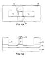
- FIGS. 1-18are pictorial representations through various views showing the processing steps employed in one embodiment of the present invention.
- Ais a top view
- Bis a cross-sectional view.
- FIG. 19is a simplistic top view of the dog-bone structure provided in FIGS. 1-18.
- FIGS. 20-32are pictorial representations through various views showing the processing steps employed in another embodiment of the present invention.
- Ais a top view
- Bis a cross-sectional view.
- FIGS. 1-18illustrate the processing steps employed in one embodiment of the present invention.
- the views containing the label “A”are top views, while the views containing the label “B” are cross-sectional views.
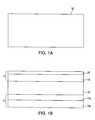
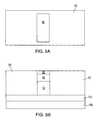
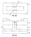
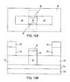
- the initial structure that is employed in the present inventionis shown, for example, in FIG. 1A (top view) and FIG. 1B (cross-sectional view).
- the initial structure shown in FIGS. 1A-1Bincludes substrate 10 having a stack comprising semiconducting body 12 , i.e., Fin, and hard mask 14 present atop substrate 10 .
- Substrate 10includes upper portion 10 u which is comprised of an insulating material such as an oxide, nitride, oxynitride or multilayers thereof, and bottom portion 10 b which is comprised of a semiconducting material such as Si.
- regions 10 and 12may be part of an SOI (silicon-on-insulator) material wherein region 10 u is a buried oxide layer which is sandwiched between semiconducting materials 10 b and 12 .
- layers 10 u and 12are layers which are separately deposited atop a semiconductor substrate.
- the semiconductor bodyi.e., Fin region 12
- the semiconductor bodyis comprised of any semiconducting material such as single crystalline Si or SiGe and hard mask 14 is comprised of a stack comprising oxide layer 16 and nitride layer 18 , respectively.
- the vertical thicknesses of semiconductor body 12 (i.e., Fin 12 ) and the hard maskare not critical to the present invention.
- semiconducting material layer 12has a vertical thickness of from about 300 to about 2000 ⁇ . . .
- hard mask 14has a vertical thickness of from about 100 to about 1000 ⁇ . . . .
- hard mask 14is formed atop a layer of semiconducting material 12 by utilizing conventional deposition processes such as chemical vapor deposition (CVD), plasma-assisted CVD, or chemical solution deposition.
- CVDchemical vapor deposition
- hard mask 14may be grown on semiconductor body 12 (i.e., Fin 12 ) utilizing a conventional thermal oxidation process, followed by a nitridation process. Both of these thermal processes, i.e., oxidation and nitridation, are well known to those skilled in the art.
- the present inventionalso contemplates forming one of the material layers of the hard mask via deposition, while forming the other material layer via a thermal oxidation/nitridation process.
- nitride layer 18is patterned utilizing conventional lithography and etching.
- the lithographic processincludes applying a photoresist to the nitride layer, exposing the photoresist to a pattern of radiation and developing the pattern into the photoresist utilizing a conventional resist developer.
- the exposed portions of the nitride layer, not protected by the patterned photoresistare removed utilizing an etching process that is highly selective in removing nitride as compare to oxide. Note that this etching step stops atop an upper surface of oxide layer 16 .
- Suitable types of etchingthat can be employed in forming the patterned nitride layer include, but are not limited to: reactive-ion etching, ion beam etching, plasma etching or laser ablation.
- the photoresistmay be removed from the structure. In some embodiments, the patterned photoresist remains on the structure throughout the subsequent etching steps.
- FIGS. 3A-3Billustrate the structure that is formed after exposed portions of oxide layer 16 , not protected by patterned nitride layer 18 , are removed utilizing an etching process that is highly selective in removing oxide as compared to nitride or semiconducting material. Note that this etching step stops atop an upper surface of underlying semiconductor body 12 .
- FIGS. 4A-4BThe resulting structure after the third etching step has been conducted is shown, for example, in FIGS. 4A-4B. It should be noted that although the drawings show the formation of one patterned semiconducting body region (capped with a patterned oxide/nitride hard mask), the present invention also contemplates forming a plurality of such patterned semiconducting body regions on the surface of insulating layer 10 u.
- insulating material 20which may, or may not, be the same as insulating layer 10 u is formed (via a conventional deposition process) atop the structure shown in FIGS. 4A and 4B and thereafter the insulating material is planarized using a conventional planarization process such as chemical-mechanical polishing (CMP) or grinding stopping on an upper surface of patterned nitride layer 18 .
- CMPchemical-mechanical polishing
- insulating material 20matches that of insulating layer 10 u .
- the resultant structure that is formed after planrizationis shown in FIGS. 5A-5B.
- the structure shown in FIGS. 5A-5Bis then subjected to a recessing step which is capable of removing a portion of insulating material 20 so as to provide the structure shown, for example, in FIGS. 6A-6B.
- This recessing stepis performed utilizing a conventional timed etching process in which a chemical etchant is employed. Note that the timed etching process exposes vertical sidewalls of patterned oxide hard mask 16 and patterned nitride hard mask 18 .
- FIGS. 7A-7Bshow the structure that is formed after planarizing layer 22 has been applied atop the structure provided in FIGS. 6A-6B.
- planarizing layer 22includes any material such as an anti-reflective coating, which is capable of forming a planarized structure.
- the planarizing materialis formed by a conventional deposition process including, but not limited to: CVD, plasma-assisted CVD, or spin-on coating. Note that in the structure shown in FIGS. 7A-7B, the planarizing layer that is present atop the patterned hard mask/semiconductor body region is thinner than the planarizing material that is formed over regions abutting the patterned hard mask/semiconductor body region.
- a conventional photoresist(labeled as 24 in the drawings) is formed atop planarizing layer 22 providing the structure shown, for example, in FIGS. 8A-8B.
- the photoresistis formed utilizing a conventional deposition process well known to those skilled in the art.
- Photoresist 24is then patterned utilizing conventional lithography so as to provide the structure shown in FIGS. 9A and 9B. Note that the patterned photoresist exposes portions of underlying planarizing layer 22 .
- the difference in reflectivity between the patterned hard mask/Fin with the thin planarizing layer and outside the Fin with the thick planarizing layercauses photoresist 24 to overexpose over Fin 12 near the edges of the gate shape.
- the overexposed regionsare labeled as 26 in FIG. 9 A.
- planarizing layer 22are then removed utilizing an etching process which is highly selective in removing the planarizing material. This etching step stops atop-an upper surface of insulating material 20 . Note that in areas over the Fin, this etching step removes all of the planarizing material stopping on an upper surface of nitride layer 18 .
- the resultant structure formed after removing portions of the planarizing layer from the structureis shown, for example, in FIGS. 10A-10B.
- FIGS. 10A-10Billustrate the structure that is formed after the removal of insulating material 20 from the structure. Note that in this structure the patterned hard mask/patterned semiconducting body region has vertical sidewalls that are now exposed.
- FIGS. 11A-11BThe structure shown in FIGS. 11A-11B is then subjected to a controlled oxide reaction (COR) etching process which undercuts oxide layer 16 remaining in the structure so as to provide a dog-bone pattern to the structure.
- the COR etching process employed in the present inventioncomprises a plasma of HF and ammonia which serves to undercut oxide layer 16 that lays beneath nitride layer 18 .
- FIGS. 12A-12Bshow the structure formed after performing the COR etching process. Note that oxide layer 16 is now trimmed and that some of insulating layer 10 u that is present beneath the semiconductor body region is recessed by the COR etching step.
- patterned photoresist 24 , remaining planarizing material 22 , and patterned nitride hard mask 18are removed from the structure utilizing conventional etching processes well known to those skilled in the art which are capable of removing those layers from the structure.
- This step of the present inventionresults in the formation of the structure shown, for example, in FIGS. 13A-13B. Note that in the resultant structure a portion of the upper horizontal surface of semiconducting body 12 not protected by trimmed oxide layer 16 is now left exposed.
- FIGS. 14A-14Bshow the structure that is formed after patterned semiconductor body 12 , i.e., the Fin, is subjected to an etching step which serves to trim the semiconductor body such that the vertical sidewalls of the semiconductor body are aligned with the vertical sidewalls of trimmed oxide layer 16 .
- This etching stepis performed utilizing a conventional dry etching process such as RIE.
- gate dielectric 30is formed about the exposed surfaces of trimmed semiconductor body 12 and the trimmed oxide mask 16 .
- the gate dielectricwhich may be comprised of an oxide, nitride, oxynitride or a multilayer thereof, is formed utilizing a conventional thermal growth process which may include oxidation, nitridation or oxynitridation.
- the thickness of the gate dielectricis not critical to the present invention, but typically gate dielectric 30 has a thickness of from about 0.8 to about 5.0 nm, with a thickness of from about 1.2 to about 2.6 nm being more highly preferred.
- the structure including gate dielectric 30is shown in FIGS. 15A-15B.
- Gate electrode 32is then formed on all exposed horizontal and vertical surfaces of the structure shown in FIGS. 15A-15B utilizing a conventional deposition process such as CVD, plasma-assisted CVD and chemical solution deposition well known in the art.
- the gate electrodeis comprised of any conventional conductor including conductive metals, conductive metal alloys, suicides and doped polysilicon.
- doped polysiliconmay be formed using an in-situ doping deposition process.
- doped polysilicon gate electrode 32may be formed by deposition and ion implantation. The resultant structure including gate electrode 32 is shown, for example, in FIGS. 16A-16B.
- FIGS. 16A-16BFollowing formation of the gate electrode, the structure shown in FIGS. 16A-16B is then subjected to a damascene gate planarization step which recesses gate electrode 32 below the upper horizontal surface of gate dielectric 30 .
- the damascene gate planarization stepis carried out utilizing a conventional etching process well known to those skilled in the art.
- the resultant structure that is formed after performing the damascene gate planarization stepis shown in FIGS. 17A-17B.
- gate dielectric 30 and hard mask 16 that are not coplanar with the damascene gate electrodeis then partially etched so as to be co-planar with the upper surface of damascene gate electrode 32 .
- this process stepdefines the final channel region 12 ′ having a dimension 1 D 1 greater than dimension 2 D 2 .
- some of insulating layer 20is recessed so as to expose regions in semiconducting layer 12 in which the source/drain regions will be subsequently formed.
- FIGS. 18A-18Bshow the resultant structure and reference number 36 is used to denote the area where source/drain regions will be formed. Further note that the resultant structure includes linear tapering portions 40 of said source/drain regions 36 that are aligned with the gate electrodes 32 edge.
- Insulating layer 20is then etched to region 10 u and doping and silicidation of the exposed source drain regions may now be performed utilizing conventional ion implantation and silicidation processes well known to those skilled in the art.
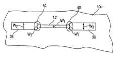
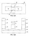
- FIG. 19shows a simplistic view of the inventive structure provided by the above processing steps.
- the structure shown in FIG. 19includes a channel region comprised of patterned semiconductor body 12 , and a source region and a drain region.
- the source/drain regionsare labeled as element 38 in FIG. 19 .
- the channel regionhas a first horizontal width, w 1
- the source and drain regionshave a second horizontal width, w 2 , that is greater than the first horizontal width.
- the source and drain regionshave tapered portions (denoted as 40 ) abutting channel region 12 with a horizontal width, w 3 , that varies in a substantially linear manner from the first horizontal width, w 1 , to the second horizontal width, w 2 .
- the above configuration of the channel region and the source/drain regionsis in the shape of a dog-bone.
- FIGS. 20-32illustrate the processing steps employed in another embodiment of the present invention.
- the views containing the label “A”are top views, while the views containing the label “B” are cross-sectional views.
- like reference numeralsare used to denote elements that correspond to elements present in FIGS. 1-18.
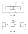
- FIGS. 20A and 20Billustrate the initial structure used in the second embodiment of the present invention.
- the initial structure shown in FIGS. 20A and 20Bwhich is the same as in FIGS. 2A-2B, includes semiconducting portion 10 b , insulating material 10 u present atop semiconducting portion 10 b , semiconducting body 12 present atop insulating material 10 u , oxide hard mark 16 present atop semiconducting body 12 , and patterned nitride hard mask 18 present atop portions of oxide hard mask 16 .
- the initial structure employed in the second embodiment of the present inventionis formed utilizing the various processing steps mentioned above in forming the structure illustrated in FIGS. 2A-2B.
- sacrificial spacers 50are then formed on exposed vertical sidewalls of patterned nitride hard mask 18 utilizing conventional deposition and etching processes well known to those skilled in the art.
- Sacrificial spacers 50are comprised of an insulating material other than an oxide.
- sacrificial spacers 50may be comprised of a nitride, oxynitride or any combination thereof.
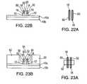
- FIGS. 22A-22Bthe structure shown in FIGS. 21A-21B is then subjected to an etching process that is highly selective in removing the exposed portions of the semiconducting body 12 that are not protected by the previously etched hard mask layers. This etching step stops atop an upper surface of insulating layer 10 u.
- Insulator 52is then formed over the structure provided in FIGS. 22A and 22B utilizing a conventional deposition process well known to those skilled in the art such as chemical vapor deposition, CVD.
- insulator 52is composed of an oxide.
- a photoresist, not shown,is then applied to the top surface of the insulator 52 and thereafter conventional lithography is employed in patterning the photoresist. With patterned photoresist atop the structure, exposed portions of insulator 52 are then removed utilizing an etching process that is highly selective in removing oxide so as to provide opening 54 in the structure.
- this etching stepdoes not remove the previously patterned regions and that after the opening is provided the patterned photoresist employed in forming the same is typically removed from the structure.
- the resultant structure formed after theses steps are performedis illustrated, for example, in FIGS. 23A and 23B.
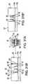
- Sacrificial spacers 50are then selectively removed utilizing a conventional-isotropic etching process so as to provide the structure shown, for example, in FIGS. 24A and 24B. Note that the patterned nitride hard mask 18 now has a width that is thinner than either underlying oxide hard mask 16 or semiconducting body 12 .
- a COR etching process as described hereinaboveis then employed to form corner rounding oxide hard mask 16 .
- This corner rounded hard maskwill subsequently provide the dog-bone configuration to the Fin.
- the structure that is formed after the COR etching step has been performedis shown, for example, in FIGS. 25A and 25B.
- the exposed portions of oxide hard mask 16 and the underlying semiconducting body, not including nitride hard mask 18are then trimmed utilizing an etching process that is highly selective in removing oxide and semiconducting material.
- the etchingmay be carried out in a single etching step, or multiple etching steps may be employed. It is noted that this step provides the dog-bone configuration to the underlying semiconducting body, i.e., Fin 12 .
- SiO2 or another like fill materialis then deposited into the opening, planarized and recessed utilizing conventional processing steps that are well known in the art so as to provide the structure shown, for example, in FIGS. 27A and 27B.
- the recessed SiO2 layeris labeled as 56 in FIGS. 27A and 27B.
- Insulative spacers 58are then formed on the exposed vertical sidewalls of insulator 52 utilizing conventional processing steps such as deposition and etching well known to those skilled in the art providing the structure shown, for example, in FIGS. 28A and 28B.
- the exposed portions of recessed SiO2 layer 56are removed utilizing an etching process that is highly selective in removing SiO2 from the structure.
- insulative spacers 58are employed as an etch mask during this processing step of the present invention and that a gate opening is provided by this step of this present invention.
- Gate dielectric 30is then formed on vertical sidewalls of any silicon surfaces utilizing a conventional deposition or thermal growing process well known to those skilled in the art.
- Gate electrode 32 including one of the above-mentioned conductorsis then formed into the gate opening and, if needed, the gate electrode is planarized utilizing a conventional planarization process providing the structure shown, for example, in FIGS. 30A and 30B.
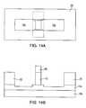
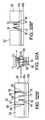
- FIGS. 31A, 31 B′ and 31 B′′A patterned mask, not shown, is formed over the structure shown in FIGS. 30A and 30B leaving selective portions of the gate electrode exposed for etching. Etching of the exposed gate electrode is then performed providing the structure shown in FIGS. 31A, 31 B′ and 31 B′′. Note that FIG. 31 B′ is a top view through cut x 1 -x 2 , while FIG. 31 B′′ is a top view through cut y 1 -y 2 .
- Silicide or other contacts 60are then formed on sidewalls of the wide Fin segments using conventional processes well known to those skilled in the art.
- the resultant structure, including contacts 60is shown in FIGS. 32A, 32 B′ and 32 B′′.
- the semiconductor structure of the present inventionincludes a plurality of FETs in which gate electrode 32 is shared between the various FETs.
Landscapes
- Thin Film Transistor (AREA)
- Insulated Gate Type Field-Effect Transistor (AREA)
Abstract
Description
Claims (8)
Priority Applications (2)
| Application Number | Priority Date | Filing Date | Title |
|---|---|---|---|
| US09/683,626US6583469B1 (en) | 2002-01-28 | 2002-01-28 | Self-aligned dog-bone structure for FinFET applications and methods to fabricate the same |
| US10/428,705US6812075B2 (en) | 2002-01-28 | 2003-05-02 | Self-aligned dog-bone structure for FinFET applications and methods to fabricate the same |
Applications Claiming Priority (1)
| Application Number | Priority Date | Filing Date | Title |
|---|---|---|---|
| US09/683,626US6583469B1 (en) | 2002-01-28 | 2002-01-28 | Self-aligned dog-bone structure for FinFET applications and methods to fabricate the same |
Related Child Applications (1)
| Application Number | Title | Priority Date | Filing Date |
|---|---|---|---|
| US10/428,705DivisionUS6812075B2 (en) | 2002-01-28 | 2003-05-02 | Self-aligned dog-bone structure for FinFET applications and methods to fabricate the same |
Publications (1)
| Publication Number | Publication Date |
|---|---|
| US6583469B1true US6583469B1 (en) | 2003-06-24 |
Family
ID=24744816
Family Applications (2)
| Application Number | Title | Priority Date | Filing Date |
|---|---|---|---|
| US09/683,626Expired - LifetimeUS6583469B1 (en) | 2002-01-28 | 2002-01-28 | Self-aligned dog-bone structure for FinFET applications and methods to fabricate the same |
| US10/428,705Expired - LifetimeUS6812075B2 (en) | 2002-01-28 | 2003-05-02 | Self-aligned dog-bone structure for FinFET applications and methods to fabricate the same |
Family Applications After (1)
| Application Number | Title | Priority Date | Filing Date |
|---|---|---|---|
| US10/428,705Expired - LifetimeUS6812075B2 (en) | 2002-01-28 | 2003-05-02 | Self-aligned dog-bone structure for FinFET applications and methods to fabricate the same |
Country Status (1)
| Country | Link |
|---|---|
| US (2) | US6583469B1 (en) |
Cited By (113)
| Publication number | Priority date | Publication date | Assignee | Title |
|---|---|---|---|---|
| US20030122186A1 (en)* | 2001-03-13 | 2003-07-03 | Nat'l. Inst. Of Advanced Indust'l Sci. And Tech. | Double-gate field-effect transistor, integrated circuit using the transistor and method of manufacturing the same |
| US20030151077A1 (en)* | 2002-02-13 | 2003-08-14 | Leo Mathew | Method of forming a vertical double gate semiconductor device and structure thereof |
| US6686231B1 (en)* | 2002-12-06 | 2004-02-03 | Advanced Micro Devices, Inc. | Damascene gate process with sacrificial oxide in semiconductor devices |
| US6716686B1 (en)* | 2003-07-08 | 2004-04-06 | Advanced Micro Devices, Inc. | Method for forming channels in a finfet device |
| US6762448B1 (en) | 2003-04-03 | 2004-07-13 | Advanced Micro Devices, Inc. | FinFET device with multiple fin structures |
| US6762483B1 (en)* | 2003-01-23 | 2004-07-13 | Advanced Micro Devices, Inc. | Narrow fin FinFET |
| US6764884B1 (en)* | 2003-04-03 | 2004-07-20 | Advanced Micro Devices, Inc. | Method for forming a gate in a FinFET device and thinning a fin in a channel region of the FinFET device |
| US6812119B1 (en)* | 2003-07-08 | 2004-11-02 | Advanced Micro Devices, Inc. | Narrow fins by oxidation in double-gate finfet |
| US20040217392A1 (en)* | 2003-04-30 | 2004-11-04 | Leo Mathew | Semiconductor fabrication process with asymmetrical conductive spacers |
| US20040235300A1 (en)* | 2003-05-22 | 2004-11-25 | Leo Mathew | Transistor with independent gate structures |
| US6831310B1 (en) | 2003-11-10 | 2004-12-14 | Freescale Semiconductor, Inc. | Integrated circuit having multiple memory types and method of formation |
| US20040253829A1 (en)* | 2003-06-14 | 2004-12-16 | Peter Friis | Methods to planarize semiconductor device and passivation layer |
| US6838347B1 (en)* | 2003-09-23 | 2005-01-04 | International Business Machines Corporation | Method for reducing line edge roughness of oxide material using chemical oxide removal |
| US20050014318A1 (en)* | 2003-01-30 | 2005-01-20 | Dirk Manger | FinFet device and method of fabrication |
| US20050020020A1 (en)* | 2002-07-16 | 2005-01-27 | Nadine Collaert | Integrated semiconductor fin device and a method for manufacturing such device |
| US6855582B1 (en) | 2003-06-12 | 2005-02-15 | Advanced Micro Devices, Inc. | FinFET gate formation using reverse trim and oxide polish |
| US6855588B1 (en)* | 2003-10-07 | 2005-02-15 | United Microelectronics Corp. | Method of fabricating a double gate MOSFET device |
| US6864164B1 (en) | 2002-12-17 | 2005-03-08 | Advanced Micro Devices, Inc. | Finfet gate formation using reverse trim of dummy gate |
| US20050057964A1 (en)* | 2003-05-22 | 2005-03-17 | Motorola Inc. | Memory with charge storage locations and adjacent gate structures |
| US20050098822A1 (en)* | 2003-11-10 | 2005-05-12 | Leo Mathew | Transistor having three electrically isolated electrodes and method of formation |
| US20050104091A1 (en)* | 2003-11-04 | 2005-05-19 | Tabery Cyrus E. | Self aligned damascene gate |
| US20050145926A1 (en)* | 2004-01-06 | 2005-07-07 | Lee Jong H. | Double-gate flash memory device and fabrication method thereof |
| US20050153492A1 (en)* | 2004-01-12 | 2005-07-14 | Ahmed Shibly S. | Damascene tri-gate FinFET |
| US20050153485A1 (en)* | 2004-01-12 | 2005-07-14 | Ahmed Shibly S. | Narrow-body damascene tri-gate FinFET |
| US20050158970A1 (en)* | 2004-01-16 | 2005-07-21 | Robert Chau | Tri-gate transistors and methods to fabricate same |
| US20050191795A1 (en)* | 2004-03-01 | 2005-09-01 | Dureseti Chidambarrao | Method of manufacture of FinFET devices with T-shaped fins and devices manufactured thereby |
| US20050233565A1 (en)* | 2004-04-15 | 2005-10-20 | International Business Machines Corporation | Methods for manufacturing a finfet using a conventional wafer and apparatus manufactured therefrom |
| US20050239242A1 (en)* | 2004-04-23 | 2005-10-27 | International Business Machines Corporation | structure and method of manufacturing a finFet device having stacked fins |
| US20050237850A1 (en)* | 2003-10-02 | 2005-10-27 | Suman Datta | Method and apparatus for improving stability of a 6T CMOS SRAM cell |
| US20050242406A1 (en)* | 2003-06-27 | 2005-11-03 | Hareland Scott A | Nonplanar device with stress incorporation layer and method of fabrication |
| US20050253193A1 (en)* | 2004-04-30 | 2005-11-17 | Taiwan Semiconductor Manufacturing Co. | Method of fabricating a necked finfet device |
| US6967175B1 (en)* | 2003-12-04 | 2005-11-22 | Advanced Micro Devices, Inc. | Damascene gate semiconductor processing with local thinning of channel region |
| US20050258477A1 (en)* | 2004-05-19 | 2005-11-24 | Tomohiro Saito | Semiconductor device and method of manufacturing the same |
| US20050269645A1 (en)* | 2004-05-14 | 2005-12-08 | Seiko Epson Corporation | Semiconductor device and method for manufacturing semiconductor device |
| US20050272192A1 (en)* | 2004-06-04 | 2005-12-08 | Chang-Woo Oh | Methods of forming fin field effect transistors using oxidation barrier layers and related devices |
| US20050282345A1 (en)* | 2004-06-18 | 2005-12-22 | Leo Mathew | Transistor with vertical dielectric structure |
| US20060033095A1 (en)* | 2004-08-10 | 2006-02-16 | Doyle Brian S | Non-planar pMOS structure with a strained channel region and an integrated strained CMOS flow |
| US20060054969A1 (en)* | 2004-09-10 | 2006-03-16 | Se-Myeong Jang | Semiconductor device having a junction extended by a selective epitaxial growth (SEG) layer and method of fabricating the same |
| US20060068591A1 (en)* | 2004-09-29 | 2006-03-30 | Marko Radosavljevic | Fabrication of channel wraparound gate structure for field-effect transistor |
| US7029959B1 (en)* | 2003-05-06 | 2006-04-18 | Advanced Micro Devices, Inc. | Source and drain protection and stringer-free gate formation in semiconductor devices |
| US20060131648A1 (en)* | 2004-12-17 | 2006-06-22 | Electronics And Telecommunications Research Institute | Ultra thin film SOI MOSFET having recessed source/drain structure and method of fabricating the same |
| US7084018B1 (en)* | 2004-05-05 | 2006-08-01 | Advanced Micro Devices, Inc. | Sacrificial oxide for minimizing box undercut in damascene FinFET |
| US20060186484A1 (en)* | 2005-02-23 | 2006-08-24 | Chau Robert S | Field effect transistor with narrow bandgap source and drain regions and method of fabrication |
| US20060197140A1 (en)* | 2005-03-04 | 2006-09-07 | Freescale Semiconductor, Inc. | Vertical transistor NVM with body contact structure and method |
| US20060214231A1 (en)* | 2004-10-25 | 2006-09-28 | Uday Shah | Nonplanar device with thinned lower body portion and method of fabrication |
| JP2006303511A (en)* | 2005-04-22 | 2006-11-02 | Korea Advanced Inst Of Sci Technol | Multi-bit non-volatile memory device having double gate structure, manufacturing method thereof, and operating method for multi-bit operation |
| US20060246685A1 (en)* | 2005-04-28 | 2006-11-02 | Tomohiro Saito | Semiconductor device fabrication method |
| US20070020855A1 (en)* | 2005-07-15 | 2007-01-25 | Samsung Electronics Co., Ltd. | Semiconductor device having vertical channels and method of manufacturing the same |
| US20070023756A1 (en)* | 2005-07-27 | 2007-02-01 | International Business Machines Corporation | Virtual body-contacted trigate |
| EP1761948A1 (en)* | 2004-06-28 | 2007-03-14 | Intel Corporation | Methods for forming semiconductor wires and resulting devices |
| US20070085134A1 (en)* | 2003-12-08 | 2007-04-19 | International Business Machines Corporation | Semiconductor memory device with increased node capacitance |
| KR100714775B1 (en)* | 2004-06-22 | 2007-05-04 | 샤프 가부시키가이샤 | Field effect transistor and fabrication method thereof |
| US20070134878A1 (en)* | 2005-12-09 | 2007-06-14 | Intel Corporation | Non-planar microelectronic device having isolation element to mitigate fringe effects and method to fabricate same |
| US20070131983A1 (en)* | 2005-12-13 | 2007-06-14 | Intel Corporation | Tri-gate integration with embedded floating body memory cell using a high-K dual metal gate |
| US20070138514A1 (en)* | 2005-12-21 | 2007-06-21 | Chang Peter L | Integration of planar and tri-gate devices on the same substrate |
| US20070148837A1 (en)* | 2005-12-27 | 2007-06-28 | Uday Shah | Method of fabricating a multi-cornered film |
| US20070148926A1 (en)* | 2005-12-28 | 2007-06-28 | Intel Corporation | Dual halo implant for improving short channel effect in three-dimensional tri-gate transistors |
| US20070158703A1 (en)* | 2006-01-06 | 2007-07-12 | Freescale Semiconductor, Inc. | Electronic device and a process for forming the electronic device |
| US20070181930A1 (en)* | 2004-08-31 | 2007-08-09 | International Business Machines Corporation | Structure and method of making double-gated self-aligned finfet having gates of different lengths |
| US20070231997A1 (en)* | 2006-03-31 | 2007-10-04 | Doyle Brian S | Stacked multi-gate transistor design and method of fabrication |
| US20070231984A1 (en)* | 2006-03-31 | 2007-10-04 | Metz Matthew V | Uniform silicide metal on epitaxially grown source and drain regions of three-dimensional transistors |
| US20070235763A1 (en)* | 2006-03-29 | 2007-10-11 | Doyle Brian S | Substrate band gap engineered multi-gate pMOS devices |
| US20070238273A1 (en)* | 2006-03-31 | 2007-10-11 | Doyle Brian S | Method of ion implanting for tri-gate devices |
| CN100361282C (en)* | 2004-03-15 | 2008-01-09 | 国际商业机器公司 | FINFET and its manufacturing method |
| US20080061383A1 (en)* | 2006-09-07 | 2008-03-13 | Elpida Memory, Inc. | Semiconductor device having fin field effect transistor and manufacturing method thereof |
| US7361958B2 (en) | 2004-09-30 | 2008-04-22 | Intel Corporation | Nonplanar transistors with metal gate electrodes |
| US20080097346A1 (en)* | 2006-09-19 | 2008-04-24 | Alcon, Inc. | Trocar cannula |
| US20080121998A1 (en)* | 2006-09-15 | 2008-05-29 | Kavalieros Jack T | Apparatus and method for selectively recessing spacers on multi-gate devices |
| US20080173942A1 (en)* | 2007-01-22 | 2008-07-24 | International Business Machines Corporation | STRUCTURE AND METHOD OF MANUFACTURING A STRAINED FinFET WITH STRESSED SILICIDE |
| US20080206934A1 (en)* | 2007-02-23 | 2008-08-28 | Jones Robert E | Forming semiconductor fins using a sacrificial fin |
| CN100428446C (en)* | 2004-06-10 | 2008-10-22 | 台湾积体电路制造股份有限公司 | Semiconductor element and manufacturing method thereof |
| US7456476B2 (en) | 2003-06-27 | 2008-11-25 | Intel Corporation | Nonplanar semiconductor device with partially or fully wrapped around gate electrode and methods of fabrication |
| US7479421B2 (en) | 2005-09-28 | 2009-01-20 | Intel Corporation | Process for integrating planar and non-planar CMOS transistors on a bulk substrate and article made thereby |
| US7491589B2 (en) | 2004-06-11 | 2009-02-17 | International Business Machines Corporation | Back gate FinFET SRAM |
| US7498225B1 (en) | 2003-12-04 | 2009-03-03 | Advanced Micro Devices, Inc. | Systems and methods for forming multiple fin structures using metal-induced-crystallization |
| EP1829114A4 (en)* | 2004-11-29 | 2009-04-08 | Texas Instruments Inc | NO REDUCED CHANNEL IN A SEMICONDUCTOR DEVICE |
| US7525160B2 (en) | 2005-12-27 | 2009-04-28 | Intel Corporation | Multigate device with recessed strain regions |
| US7547637B2 (en) | 2005-06-21 | 2009-06-16 | Intel Corporation | Methods for patterning a semiconductor film |
| US20090159967A1 (en)* | 2007-12-19 | 2009-06-25 | Henry Litzmann Edwards | Semiconductor device having various widths under gate |
| US20090179251A1 (en)* | 2008-01-11 | 2009-07-16 | International Business Machines Corporation | Device and design structures for memory cells in a non-volatile random access memory and methods of fabricating such device structures |
| US20090179268A1 (en)* | 2008-01-11 | 2009-07-16 | International Business Machines Corporation | Design structures for high-voltage integrated circuits |
| US20090179266A1 (en)* | 2008-01-11 | 2009-07-16 | International Business Machines Corporation | Device structures for a metal-oxide-semiconductor field effect transistor and methods of fabricating such device structures |
| US20090179267A1 (en)* | 2008-01-11 | 2009-07-16 | International Business Machines Corporation | Semiconductor-on-insulator high-voltage device structures, methods of fabricating such device structures, and design structures for high-voltage circuits |
| US7563701B2 (en) | 2005-03-31 | 2009-07-21 | Intel Corporation | Self-aligned contacts for transistors |
| US7579280B2 (en) | 2004-06-01 | 2009-08-25 | Intel Corporation | Method of patterning a film |
| US20090294919A1 (en)* | 2008-05-30 | 2009-12-03 | Stephens Tab A | Method of forming a finfet and structure |
| US20100019321A1 (en)* | 2005-09-27 | 2010-01-28 | Young Kyun Cho | MULTIPLE-GATE MOS TRANSISTOR USING Si SUBSTRATE AND METHOD OF MANUFACTURING THE SAME |
| US7679134B1 (en) | 2002-11-26 | 2010-03-16 | Globalfoundries | FinFET device with multiple fin structures |
| US20100065888A1 (en)* | 2004-06-30 | 2010-03-18 | Shaheen Mohamad A | High mobility tri-gate devices and methods of fabrication |
| US7700470B2 (en) | 2006-09-22 | 2010-04-20 | Intel Corporation | Selective anisotropic wet etching of workfunction metal for semiconductor devices |
| US7736956B2 (en) | 2005-08-17 | 2010-06-15 | Intel Corporation | Lateral undercut of metal gate in SOI device |
| US20100155801A1 (en)* | 2008-12-22 | 2010-06-24 | Doyle Brian S | Integrated circuit, 1T-1C embedded memory cell containing same, and method of manufacturing 1T-1C memory cell for embedded memory application |
| US20100163945A1 (en)* | 2008-12-30 | 2010-07-01 | Kavalieros Jack T | Embedded memory cell and method of manufacturing same |
| US7781771B2 (en) | 2004-03-31 | 2010-08-24 | Intel Corporation | Bulk non-planar transistor having strained enhanced mobility and methods of fabrication |
| US7859053B2 (en) | 2004-09-29 | 2010-12-28 | Intel Corporation | Independently accessed double-gate and tri-gate transistors in same process flow |
| US20110018063A1 (en)* | 2008-03-14 | 2011-01-27 | Brian Doyle | Apparatus and methods for improving multi-gate device performance |
| US7879675B2 (en) | 2005-03-14 | 2011-02-01 | Intel Corporation | Field effect transistor with metal source/drain regions |
| US7898041B2 (en) | 2005-06-30 | 2011-03-01 | Intel Corporation | Block contact architectures for nanoscale channel transistors |
| US7902014B2 (en) | 2005-09-28 | 2011-03-08 | Intel Corporation | CMOS devices with a single work function gate electrode and method of fabrication |
| US7989280B2 (en) | 2005-11-30 | 2011-08-02 | Intel Corporation | Dielectric interface for group III-V semiconductor device |
| US20120007183A1 (en)* | 2010-07-08 | 2012-01-12 | International Business Machines Corporation | Multi-gate Transistor Having Sidewall Contacts |
| US20120119267A1 (en)* | 2010-11-17 | 2012-05-17 | Fujitsu Semiconductor Limited | Semiconductor device production method and semiconductor device |
| US8362566B2 (en) | 2008-06-23 | 2013-01-29 | Intel Corporation | Stress in trigate devices using complimentary gate fill materials |
| US20130154010A1 (en)* | 2006-05-15 | 2013-06-20 | Carnegie Mellon University | Integrated Circuit Device, System, and Method of Fabrication |
| CN103367442A (en)* | 2012-03-28 | 2013-10-23 | 台湾积体电路制造股份有限公司 | Gate stack of fin field effect transistor |
| US8617945B2 (en) | 2006-08-02 | 2013-12-31 | Intel Corporation | Stacking fault and twin blocking barrier for integrating III-V on Si |
| US9337307B2 (en) | 2005-06-15 | 2016-05-10 | Intel Corporation | Method for fabricating transistor with thinned channel |
| US20170194325A1 (en)* | 2015-06-30 | 2017-07-06 | International Business Machines Corporation | FINFET with U-Shaped Channel |
| US9711410B2 (en) | 2011-12-22 | 2017-07-18 | Intel Corporation | Semiconductor device having a necked semiconductor body and method of forming semiconductor bodies of varying width |
| US9935102B1 (en) | 2016-10-05 | 2018-04-03 | International Business Machines Corporation | Method and structure for improving vertical transistor |
| US10056486B2 (en)* | 2016-03-24 | 2018-08-21 | Globalfoundries Inc. | Methods for fin thinning providing improved SCE and S/D EPI growth |
| US10074732B1 (en) | 2017-06-14 | 2018-09-11 | Globalfoundries Inc. | Methods of forming short channel and long channel finFET devices so as to adjust threshold voltages |
| US20210167192A1 (en)* | 2014-03-28 | 2021-06-03 | Taiwan Semiconductor Manufacturing Co., Ltd. | FinFETs With Low Source/Drain Contact Resistance |
Families Citing this family (27)
| Publication number | Priority date | Publication date | Assignee | Title |
|---|---|---|---|---|
| KR100517559B1 (en)* | 2003-06-27 | 2005-09-28 | 삼성전자주식회사 | Fin field effect transistor and method for forming of fin therein |
| GB2403810B (en)* | 2003-07-10 | 2005-06-08 | Schlumberger Holdings | Method and apparatus for imaging earth formation |
| US6924178B2 (en)* | 2003-12-08 | 2005-08-02 | International Business Machines Corporation | Oxide/nitride stacked in FinFET spacer process |
| KR100598099B1 (en)* | 2004-02-24 | 2006-07-07 | 삼성전자주식회사 | Vertical channel fin field effect transistor with damascene gate and method of manufacturing same |
| KR20050108916A (en)* | 2004-05-14 | 2005-11-17 | 삼성전자주식회사 | Methods of forming a fin field effect transistor using damascene process |
| KR100560818B1 (en)* | 2004-06-02 | 2006-03-13 | 삼성전자주식회사 | Semiconductor device and manufacturing method thereof |
| TWI283066B (en)* | 2004-09-07 | 2007-06-21 | Samsung Electronics Co Ltd | Field effect transistor (FET) having wire channels and method of fabricating the same |
| KR100585157B1 (en)* | 2004-09-07 | 2006-05-30 | 삼성전자주식회사 | Morse transistors having a plurality of wire bridge channels and manufacturing method thereof |
| US6995051B1 (en)* | 2004-10-28 | 2006-02-07 | International Business Machines Corporation | Irradiation assisted reactive ion etching |
| TWI295506B (en) | 2005-02-03 | 2008-04-01 | Samsung Electronics Co Ltd | Semiconductor device having transistor with vertical gate electrode and method of fabricating the same |
| US7488650B2 (en)* | 2005-02-18 | 2009-02-10 | Infineon Technologies Ag | Method of forming trench-gate electrode for FinFET device |
| KR100666368B1 (en)* | 2005-08-09 | 2007-01-09 | 삼성전자주식회사 | Transistors and manufacturing methods thereof |
| US7309626B2 (en)* | 2005-11-15 | 2007-12-18 | International Business Machines Corporation | Quasi self-aligned source/drain FinFET process |
| US7811890B2 (en)* | 2006-10-11 | 2010-10-12 | Macronix International Co., Ltd. | Vertical channel transistor structure and manufacturing method thereof |
| US8772858B2 (en) | 2006-10-11 | 2014-07-08 | Macronix International Co., Ltd. | Vertical channel memory and manufacturing method thereof and operating method using the same |
| US7851848B2 (en)* | 2006-11-01 | 2010-12-14 | Macronix International Co., Ltd. | Cylindrical channel charge trapping devices with effectively high coupling ratios |
| US7838923B2 (en)* | 2007-08-09 | 2010-11-23 | Macronix International Co., Ltd. | Lateral pocket implant charge trapping devices |
| JP2009158813A (en)* | 2007-12-27 | 2009-07-16 | Elpida Memory Inc | Semiconductor device manufacturing method and semiconductor device |
| US7872303B2 (en)* | 2008-08-14 | 2011-01-18 | International Business Machines Corporation | FinFET with longitudinal stress in a channel |
| US8860124B2 (en)* | 2009-01-15 | 2014-10-14 | Macronix International Co., Ltd. | Depletion-mode charge-trapping flash device |
| CN103137478A (en)* | 2011-11-21 | 2013-06-05 | 中芯国际集成电路制造(上海)有限公司 | Manufacturing method and structure of fin field-effect transistor (FinFET) device |
| US8912606B2 (en) | 2012-04-24 | 2014-12-16 | Globalfoundries Inc. | Integrated circuits having protruding source and drain regions and methods for forming integrated circuits |
| US9793378B2 (en) | 2013-05-31 | 2017-10-17 | Stmicroelectronics, Inc. | Fin field effect transistor device with reduced overlap capacitance and enhanced mechanical stability |
| US9263554B2 (en) | 2013-06-04 | 2016-02-16 | International Business Machines Corporation | Localized fin width scaling using a hydrogen anneal |
| US9112032B1 (en)* | 2014-06-16 | 2015-08-18 | Globalfoundries Inc. | Methods of forming replacement gate structures on semiconductor devices |
| US9524987B2 (en)* | 2014-10-21 | 2016-12-20 | United Microelectronics Corp. | Fin-shaped structure and method thereof |
| US9799660B1 (en) | 2016-05-11 | 2017-10-24 | Globalfoundries Inc. | Stable and reliable FinFET SRAM with improved beta ratio |
Citations (9)
| Publication number | Priority date | Publication date | Assignee | Title |
|---|---|---|---|---|
| US4636829A (en) | 1983-08-18 | 1987-01-13 | Itt Industries, Inc. | Photodetector integrated circuit |
| US5067002A (en) | 1987-01-30 | 1991-11-19 | Motorola, Inc. | Integrated circuit structures having polycrystalline electrode contacts |
| US5087951A (en) | 1988-05-02 | 1992-02-11 | Micron Technology | Semiconductor memory device transistor and cell structure |
| US5521410A (en) | 1993-03-22 | 1996-05-28 | Nec Corporation | Power semiconductor device comprising vertical double-diffused MOSFETS each having low on-resistance per unit area |
| US5777362A (en) | 1995-06-07 | 1998-07-07 | Harris Corporation | High efficiency quasi-vertical DMOS in CMOS or BICMOS process |
| US6194763B1 (en) | 1996-12-26 | 2001-02-27 | Hitachi, Ltd. | Semiconductor device having SOI-MOSFET |
| US6246973B1 (en) | 1998-08-14 | 2001-06-12 | Motorola, Inc. | Modeling method of MOSFET |
| US6413802B1 (en)* | 2000-10-23 | 2002-07-02 | The Regents Of The University Of California | Finfet transistor structures having a double gate channel extending vertically from a substrate and methods of manufacture |
| US6429538B1 (en)* | 2000-11-30 | 2002-08-06 | Taiwan Semiconductor Manufacturing Company | Method for making a novel graded silicon nitride/silicon oxide (SNO) hard mask for improved deep sub-micrometer semiconductor processing |
Family Cites Families (1)
| Publication number | Priority date | Publication date | Assignee | Title |
|---|---|---|---|---|
| US6562665B1 (en)* | 2000-10-16 | 2003-05-13 | Advanced Micro Devices, Inc. | Fabrication of a field effect transistor with a recess in a semiconductor pillar in SOI technology |
- 2002
- 2002-01-28USUS09/683,626patent/US6583469B1/ennot_activeExpired - Lifetime
- 2003
- 2003-05-02USUS10/428,705patent/US6812075B2/ennot_activeExpired - Lifetime
Patent Citations (9)
| Publication number | Priority date | Publication date | Assignee | Title |
|---|---|---|---|---|
| US4636829A (en) | 1983-08-18 | 1987-01-13 | Itt Industries, Inc. | Photodetector integrated circuit |
| US5067002A (en) | 1987-01-30 | 1991-11-19 | Motorola, Inc. | Integrated circuit structures having polycrystalline electrode contacts |
| US5087951A (en) | 1988-05-02 | 1992-02-11 | Micron Technology | Semiconductor memory device transistor and cell structure |
| US5521410A (en) | 1993-03-22 | 1996-05-28 | Nec Corporation | Power semiconductor device comprising vertical double-diffused MOSFETS each having low on-resistance per unit area |
| US5777362A (en) | 1995-06-07 | 1998-07-07 | Harris Corporation | High efficiency quasi-vertical DMOS in CMOS or BICMOS process |
| US6194763B1 (en) | 1996-12-26 | 2001-02-27 | Hitachi, Ltd. | Semiconductor device having SOI-MOSFET |
| US6246973B1 (en) | 1998-08-14 | 2001-06-12 | Motorola, Inc. | Modeling method of MOSFET |
| US6413802B1 (en)* | 2000-10-23 | 2002-07-02 | The Regents Of The University Of California | Finfet transistor structures having a double gate channel extending vertically from a substrate and methods of manufacture |
| US6429538B1 (en)* | 2000-11-30 | 2002-08-06 | Taiwan Semiconductor Manufacturing Company | Method for making a novel graded silicon nitride/silicon oxide (SNO) hard mask for improved deep sub-micrometer semiconductor processing |
Non-Patent Citations (2)
| Title |
|---|
| Jong-Ho Lee, et al., "Super Self-Aligned Double-Gate (SSDG) MOSFET's Utilizing Oxidation Rate Difference and Selective Epitaxy", Microsystems Technology Laboratories, Massachusetts Institute of Technology, Cambridge, MA. |
| Yang, et al., "Scaling the Si MOSFET: From Bulk SOI to Bulk", IEEE Transactions on Electron Devices, vol. 39, No. 7, Jul. 1992. |
Cited By (262)
| Publication number | Priority date | Publication date | Assignee | Title |
|---|---|---|---|---|
| US20030122186A1 (en)* | 2001-03-13 | 2003-07-03 | Nat'l. Inst. Of Advanced Indust'l Sci. And Tech. | Double-gate field-effect transistor, integrated circuit using the transistor and method of manufacturing the same |
| US7061055B2 (en)* | 2001-03-13 | 2006-06-13 | National Institute Of Advanced Industrial Science And Technology | Double-gate field-effect transistor, integrated circuit using the transistor and method of manufacturing the same |
| US20030151077A1 (en)* | 2002-02-13 | 2003-08-14 | Leo Mathew | Method of forming a vertical double gate semiconductor device and structure thereof |
| US6974729B2 (en)* | 2002-07-16 | 2005-12-13 | Interuniversitair Microelektronica Centrum (Imec) | Integrated semiconductor fin device and a method for manufacturing such device |
| US20050020020A1 (en)* | 2002-07-16 | 2005-01-27 | Nadine Collaert | Integrated semiconductor fin device and a method for manufacturing such device |
| US7679134B1 (en) | 2002-11-26 | 2010-03-16 | Globalfoundries | FinFET device with multiple fin structures |
| US7256455B2 (en) | 2002-12-06 | 2007-08-14 | Advanced Micro Devices, Inc. | Double gate semiconductor device having a metal gate |
| US6686231B1 (en)* | 2002-12-06 | 2004-02-03 | Advanced Micro Devices, Inc. | Damascene gate process with sacrificial oxide in semiconductor devices |
| US20040110097A1 (en)* | 2002-12-06 | 2004-06-10 | Ahmed Shibly S. | Double gate semiconductor device having a metal gate |
| US6864164B1 (en) | 2002-12-17 | 2005-03-08 | Advanced Micro Devices, Inc. | Finfet gate formation using reverse trim of dummy gate |
| US6762483B1 (en)* | 2003-01-23 | 2004-07-13 | Advanced Micro Devices, Inc. | Narrow fin FinFET |
| US20040197975A1 (en)* | 2003-01-23 | 2004-10-07 | Zoran Krivokapic | Narrow fin finfet |
| US6921963B2 (en) | 2003-01-23 | 2005-07-26 | Advanced Micro Devices, Inc | Narrow fin FinFET |
| US7074660B2 (en)* | 2003-01-30 | 2006-07-11 | Infineon Technologies Ag | FinFet device and method of fabrication |
| US20050014318A1 (en)* | 2003-01-30 | 2005-01-20 | Dirk Manger | FinFet device and method of fabrication |
| US6764884B1 (en)* | 2003-04-03 | 2004-07-20 | Advanced Micro Devices, Inc. | Method for forming a gate in a FinFET device and thinning a fin in a channel region of the FinFET device |
| US6762448B1 (en) | 2003-04-03 | 2004-07-13 | Advanced Micro Devices, Inc. | FinFET device with multiple fin structures |
| KR101079348B1 (en)* | 2003-04-03 | 2011-11-04 | 어드밴스드 마이크로 디바이시즈, 인코포레이티드 | Method for forming a gate in a finfet device and thinning a fin in a channel region of the finfet device |
| US6852576B2 (en) | 2003-04-03 | 2005-02-08 | Advanced Micro Devices, Inc. | Method for forming structures in finfet devices |
| US20040198031A1 (en)* | 2003-04-03 | 2004-10-07 | Ming-Ren Lin | Method for forming structures in finfet devices |
| US20040217392A1 (en)* | 2003-04-30 | 2004-11-04 | Leo Mathew | Semiconductor fabrication process with asymmetrical conductive spacers |
| US6967143B2 (en) | 2003-04-30 | 2005-11-22 | Freescale Semiconductor, Inc. | Semiconductor fabrication process with asymmetrical conductive spacers |
| US7029959B1 (en)* | 2003-05-06 | 2006-04-18 | Advanced Micro Devices, Inc. | Source and drain protection and stringer-free gate formation in semiconductor devices |
| US7192876B2 (en) | 2003-05-22 | 2007-03-20 | Freescale Semiconductor, Inc. | Transistor with independent gate structures |
| US20040235300A1 (en)* | 2003-05-22 | 2004-11-25 | Leo Mathew | Transistor with independent gate structures |
| US20050057964A1 (en)* | 2003-05-22 | 2005-03-17 | Motorola Inc. | Memory with charge storage locations and adjacent gate structures |
| US6903967B2 (en) | 2003-05-22 | 2005-06-07 | Freescale Semiconductor, Inc. | Memory with charge storage locations and adjacent gate structures |
| US6855582B1 (en) | 2003-06-12 | 2005-02-15 | Advanced Micro Devices, Inc. | FinFET gate formation using reverse trim and oxide polish |
| US6987068B2 (en)* | 2003-06-14 | 2006-01-17 | Intel Corporation | Methods to planarize semiconductor device and passivation layer |
| US20040253829A1 (en)* | 2003-06-14 | 2004-12-16 | Peter Friis | Methods to planarize semiconductor device and passivation layer |
| US20050242406A1 (en)* | 2003-06-27 | 2005-11-03 | Hareland Scott A | Nonplanar device with stress incorporation layer and method of fabrication |
| US8405164B2 (en) | 2003-06-27 | 2013-03-26 | Intel Corporation | Tri-gate transistor device with stress incorporation layer and method of fabrication |
| US8273626B2 (en) | 2003-06-27 | 2012-09-25 | Intel Corporationn | Nonplanar semiconductor device with partially or fully wrapped around gate electrode and methods of fabrication |
| US7820513B2 (en) | 2003-06-27 | 2010-10-26 | Intel Corporation | Nonplanar semiconductor device with partially or fully wrapped around gate electrode and methods of fabrication |
| US20060261411A1 (en)* | 2003-06-27 | 2006-11-23 | Hareland Scott A | Nonplanar device with stress incorporation layer and method of fabrication |
| US7714397B2 (en) | 2003-06-27 | 2010-05-11 | Intel Corporation | Tri-gate transistor device with stress incorporation layer and method of fabrication |
| US7241653B2 (en) | 2003-06-27 | 2007-07-10 | Intel Corporation | Nonplanar device with stress incorporation layer and method of fabrication |
| US7456476B2 (en) | 2003-06-27 | 2008-11-25 | Intel Corporation | Nonplanar semiconductor device with partially or fully wrapped around gate electrode and methods of fabrication |
| US7432557B1 (en) | 2003-07-08 | 2008-10-07 | Advanced Micro Devices, Inc. | FinFET device with multiple channels |
| US6716686B1 (en)* | 2003-07-08 | 2004-04-06 | Advanced Micro Devices, Inc. | Method for forming channels in a finfet device |
| US6812119B1 (en)* | 2003-07-08 | 2004-11-02 | Advanced Micro Devices, Inc. | Narrow fins by oxidation in double-gate finfet |
| US6838347B1 (en)* | 2003-09-23 | 2005-01-04 | International Business Machines Corporation | Method for reducing line edge roughness of oxide material using chemical oxide removal |
| US7445980B2 (en) | 2003-10-02 | 2008-11-04 | Intel Corporation | Method and apparatus for improving stability of a 6T CMOS SRAM cell |
| US20060281236A1 (en)* | 2003-10-02 | 2006-12-14 | Suman Datta | Method and apparatus for improving stability of a 6T CMOS SRAM cell |
| US20050237850A1 (en)* | 2003-10-02 | 2005-10-27 | Suman Datta | Method and apparatus for improving stability of a 6T CMOS SRAM cell |
| US6855588B1 (en)* | 2003-10-07 | 2005-02-15 | United Microelectronics Corp. | Method of fabricating a double gate MOSFET device |
| GB2424517B (en)* | 2003-11-04 | 2007-07-11 | Advanced Micro Devices Inc | Self aligned damascene gate |
| CN100524655C (en)* | 2003-11-04 | 2009-08-05 | 先进微装置公司 | self-aligned damascene gate |
| WO2005048339A1 (en)* | 2003-11-04 | 2005-05-26 | Advanced Micro Devices, Inc. | Self aligned damascene gate |
| US20050104091A1 (en)* | 2003-11-04 | 2005-05-19 | Tabery Cyrus E. | Self aligned damascene gate |
| KR101112046B1 (en)* | 2003-11-04 | 2012-02-27 | 글로벌파운드리즈 인크. | Self aligned damascene gate |
| GB2424517A (en)* | 2003-11-04 | 2006-09-27 | Advanced Micro Devices Inc | Self aligned damascene gate |
| US7029958B2 (en) | 2003-11-04 | 2006-04-18 | Advanced Micro Devices, Inc. | Self aligned damascene gate |
| US20050098822A1 (en)* | 2003-11-10 | 2005-05-12 | Leo Mathew | Transistor having three electrically isolated electrodes and method of formation |
| US7098502B2 (en) | 2003-11-10 | 2006-08-29 | Freescale Semiconductor, Inc. | Transistor having three electrically isolated electrodes and method of formation |
| US6831310B1 (en) | 2003-11-10 | 2004-12-14 | Freescale Semiconductor, Inc. | Integrated circuit having multiple memory types and method of formation |
| US7498225B1 (en) | 2003-12-04 | 2009-03-03 | Advanced Micro Devices, Inc. | Systems and methods for forming multiple fin structures using metal-induced-crystallization |
| US6967175B1 (en)* | 2003-12-04 | 2005-11-22 | Advanced Micro Devices, Inc. | Damascene gate semiconductor processing with local thinning of channel region |
| US20070085134A1 (en)* | 2003-12-08 | 2007-04-19 | International Business Machines Corporation | Semiconductor memory device with increased node capacitance |
| US7352025B2 (en)* | 2003-12-08 | 2008-04-01 | International Business Machines Corporation | Semiconductor memory device with increased node capacitance |
| US7005700B2 (en)* | 2004-01-06 | 2006-02-28 | Jong Ho Lee | Double-gate flash memory device |
| US20050145926A1 (en)* | 2004-01-06 | 2005-07-07 | Lee Jong H. | Double-gate flash memory device and fabrication method thereof |
| US20050153492A1 (en)* | 2004-01-12 | 2005-07-14 | Ahmed Shibly S. | Damascene tri-gate FinFET |
| US7041542B2 (en) | 2004-01-12 | 2006-05-09 | Advanced Micro Devices, Inc. | Damascene tri-gate FinFET |
| US7186599B2 (en)* | 2004-01-12 | 2007-03-06 | Advanced Micro Devices, Inc. | Narrow-body damascene tri-gate FinFET |
| US20050153485A1 (en)* | 2004-01-12 | 2005-07-14 | Ahmed Shibly S. | Narrow-body damascene tri-gate FinFET |
| US20050158970A1 (en)* | 2004-01-16 | 2005-07-21 | Robert Chau | Tri-gate transistors and methods to fabricate same |
| US7060539B2 (en) | 2004-03-01 | 2006-06-13 | International Business Machines Corporation | Method of manufacture of FinFET devices with T-shaped fins and devices manufactured thereby |
| US20050191795A1 (en)* | 2004-03-01 | 2005-09-01 | Dureseti Chidambarrao | Method of manufacture of FinFET devices with T-shaped fins and devices manufactured thereby |
| CN100361282C (en)* | 2004-03-15 | 2008-01-09 | 国际商业机器公司 | FINFET and its manufacturing method |
| US7781771B2 (en) | 2004-03-31 | 2010-08-24 | Intel Corporation | Bulk non-planar transistor having strained enhanced mobility and methods of fabrication |
| US7800152B2 (en) | 2004-04-15 | 2010-09-21 | International Business Machines Corporation | Methods for manufacturing a finfet using a conventional wafer and apparatus manufactured therefrom |
| US7262084B2 (en) | 2004-04-15 | 2007-08-28 | International Business Machines Corporation | Methods for manufacturing a finFET using a conventional wafer and apparatus manufactured therefrom |
| US20050233565A1 (en)* | 2004-04-15 | 2005-10-20 | International Business Machines Corporation | Methods for manufacturing a finfet using a conventional wafer and apparatus manufactured therefrom |
| US7098477B2 (en) | 2004-04-23 | 2006-08-29 | International Business Machines Corporation | Structure and method of manufacturing a finFET device having stacked fins |
| US20050239242A1 (en)* | 2004-04-23 | 2005-10-27 | International Business Machines Corporation | structure and method of manufacturing a finFet device having stacked fins |
| US20070063261A1 (en)* | 2004-04-30 | 2007-03-22 | Taiwan Semiconductor Manufacturing Company, Ltd. | Necked Finfet device |
| US20050253193A1 (en)* | 2004-04-30 | 2005-11-17 | Taiwan Semiconductor Manufacturing Co. | Method of fabricating a necked finfet device |
| US7122412B2 (en)* | 2004-04-30 | 2006-10-17 | Taiwan Semiconductor Manufacturing Company, Ltd. | Method of fabricating a necked FINFET device |
| US7084018B1 (en)* | 2004-05-05 | 2006-08-01 | Advanced Micro Devices, Inc. | Sacrificial oxide for minimizing box undercut in damascene FinFET |
| US20050269645A1 (en)* | 2004-05-14 | 2005-12-08 | Seiko Epson Corporation | Semiconductor device and method for manufacturing semiconductor device |
| US7563665B2 (en)* | 2004-05-14 | 2009-07-21 | Seiko Epson Corporation | Semiconductor device and method for manufacturing semiconductor device |
| US20070007594A1 (en)* | 2004-05-19 | 2007-01-11 | Kabushiki Kaisha Toshiba | Semiconductor device and method of manufacturing the same |
| US20050258477A1 (en)* | 2004-05-19 | 2005-11-24 | Tomohiro Saito | Semiconductor device and method of manufacturing the same |
| US7166895B2 (en)* | 2004-05-19 | 2007-01-23 | Kabushiki Kaisha Toshiba | Semiconductor device including insulating film having a convex portion |
| US7422947B2 (en) | 2004-05-19 | 2008-09-09 | Kabushiki Kaisha Toshiba | Semiconductor device and method of manufacturing the same |
| US7579280B2 (en) | 2004-06-01 | 2009-08-25 | Intel Corporation | Method of patterning a film |
| US7297600B2 (en) | 2004-06-04 | 2007-11-20 | Samsung Electronics Co., Ltd. | Methods of forming fin field effect transistors using oxidation barrier layers |
| US20080029828A1 (en)* | 2004-06-04 | 2008-02-07 | Samsung Electronics Co., Ltd. | Fin field effect transistors including oxidation barrier layers |
| US20050272192A1 (en)* | 2004-06-04 | 2005-12-08 | Chang-Woo Oh | Methods of forming fin field effect transistors using oxidation barrier layers and related devices |
| US7745871B2 (en) | 2004-06-04 | 2010-06-29 | Chang-Woo Oh | Fin field effect transistors including oxidation barrier layers |
| CN100428446C (en)* | 2004-06-10 | 2008-10-22 | 台湾积体电路制造股份有限公司 | Semiconductor element and manufacturing method thereof |
| US7491589B2 (en) | 2004-06-11 | 2009-02-17 | International Business Machines Corporation | Back gate FinFET SRAM |
| US7018876B2 (en) | 2004-06-18 | 2006-03-28 | Freescale Semiconductor, Inc. | Transistor with vertical dielectric structure |
| US20050282345A1 (en)* | 2004-06-18 | 2005-12-22 | Leo Mathew | Transistor with vertical dielectric structure |
| KR100714775B1 (en)* | 2004-06-22 | 2007-05-04 | 샤프 가부시키가이샤 | Field effect transistor and fabrication method thereof |
| EP1761948A1 (en)* | 2004-06-28 | 2007-03-14 | Intel Corporation | Methods for forming semiconductor wires and resulting devices |
| US20100065888A1 (en)* | 2004-06-30 | 2010-03-18 | Shaheen Mohamad A | High mobility tri-gate devices and methods of fabrication |
| US8084818B2 (en) | 2004-06-30 | 2011-12-27 | Intel Corporation | High mobility tri-gate devices and methods of fabrication |
| US20060033095A1 (en)* | 2004-08-10 | 2006-02-16 | Doyle Brian S | Non-planar pMOS structure with a strained channel region and an integrated strained CMOS flow |
| US7960794B2 (en) | 2004-08-10 | 2011-06-14 | Intel Corporation | Non-planar pMOS structure with a strained channel region and an integrated strained CMOS flow |
| US7348284B2 (en) | 2004-08-10 | 2008-03-25 | Intel Corporation | Non-planar pMOS structure with a strained channel region and an integrated strained CMOS flow |
| US7348641B2 (en) | 2004-08-31 | 2008-03-25 | International Business Machines Corporation | Structure and method of making double-gated self-aligned finFET having gates of different lengths |
| US20080176365A1 (en)* | 2004-08-31 | 2008-07-24 | Huilong Zhu | Method of making double-gated self-aligned finFET having gates of different lengths |
| US7785944B2 (en) | 2004-08-31 | 2010-08-31 | International Business Machines Corporation | Method of making double-gated self-aligned finFET having gates of different lengths |
| US20070181930A1 (en)* | 2004-08-31 | 2007-08-09 | International Business Machines Corporation | Structure and method of making double-gated self-aligned finfet having gates of different lengths |
| US7592686B2 (en) | 2004-09-10 | 2009-09-22 | Samsung Electronics Co., Ltd. | Semiconductor device having a junction extended by a selective epitaxial growth (SEG) layer and method of fabricating the same |
| US7803684B2 (en) | 2004-09-10 | 2010-09-28 | Samsung Electronics Co., Ltd. | Method of fabricating semiconductor device having a junction extended by a selective epitaxial growth (SEG) layer |
| US20060054969A1 (en)* | 2004-09-10 | 2006-03-16 | Se-Myeong Jang | Semiconductor device having a junction extended by a selective epitaxial growth (SEG) layer and method of fabricating the same |
| US20100015768A1 (en)* | 2004-09-10 | 2010-01-21 | Samsung Electronics Co., Ltd. | Method of fabricating semiconductor device having a junction extended by a selective epitaxial growth (SEG) layer |
| US8399922B2 (en) | 2004-09-29 | 2013-03-19 | Intel Corporation | Independently accessed double-gate and tri-gate transistors |
| US7859053B2 (en) | 2004-09-29 | 2010-12-28 | Intel Corporation | Independently accessed double-gate and tri-gate transistors in same process flow |
| US8268709B2 (en) | 2004-09-29 | 2012-09-18 | Intel Corporation | Independently accessed double-gate and tri-gate transistors in same process flow |
| US7915167B2 (en) | 2004-09-29 | 2011-03-29 | Intel Corporation | Fabrication of channel wraparound gate structure for field-effect transistor |
| US20060068591A1 (en)* | 2004-09-29 | 2006-03-30 | Marko Radosavljevic | Fabrication of channel wraparound gate structure for field-effect transistor |
| US7361958B2 (en) | 2004-09-30 | 2008-04-22 | Intel Corporation | Nonplanar transistors with metal gate electrodes |
| US7528025B2 (en) | 2004-09-30 | 2009-05-05 | Intel Corporation | Nonplanar transistors with metal gate electrodes |
| US9741809B2 (en) | 2004-10-25 | 2017-08-22 | Intel Corporation | Nonplanar device with thinned lower body portion and method of fabrication |
| US8067818B2 (en) | 2004-10-25 | 2011-11-29 | Intel Corporation | Nonplanar device with thinned lower body portion and method of fabrication |
| US7550333B2 (en) | 2004-10-25 | 2009-06-23 | Intel Corporation | Nonplanar device with thinned lower body portion and method of fabrication |
| US9190518B2 (en) | 2004-10-25 | 2015-11-17 | Intel Corporation | Nonplanar device with thinned lower body portion and method of fabrication |
| US8749026B2 (en) | 2004-10-25 | 2014-06-10 | Intel Corporation | Nonplanar device with thinned lower body portion and method of fabrication |
| US20060214231A1 (en)* | 2004-10-25 | 2006-09-28 | Uday Shah | Nonplanar device with thinned lower body portion and method of fabrication |
| US10236356B2 (en) | 2004-10-25 | 2019-03-19 | Intel Corporation | Nonplanar device with thinned lower body portion and method of fabrication |
| US8502351B2 (en) | 2004-10-25 | 2013-08-06 | Intel Corporation | Nonplanar device with thinned lower body portion and method of fabrication |
| EP1829114A4 (en)* | 2004-11-29 | 2009-04-08 | Texas Instruments Inc | NO REDUCED CHANNEL IN A SEMICONDUCTOR DEVICE |
| US20060131648A1 (en)* | 2004-12-17 | 2006-06-22 | Electronics And Telecommunications Research Institute | Ultra thin film SOI MOSFET having recessed source/drain structure and method of fabricating the same |
| US7518196B2 (en) | 2005-02-23 | 2009-04-14 | Intel Corporation | Field effect transistor with narrow bandgap source and drain regions and method of fabrication |
| US8368135B2 (en) | 2005-02-23 | 2013-02-05 | Intel Corporation | Field effect transistor with narrow bandgap source and drain regions and method of fabrication |
| US7893506B2 (en) | 2005-02-23 | 2011-02-22 | Intel Corporation | Field effect transistor with narrow bandgap source and drain regions and method of fabrication |
| US9368583B2 (en) | 2005-02-23 | 2016-06-14 | Intel Corporation | Field effect transistor with narrow bandgap source and drain regions and method of fabrication |
| US8183646B2 (en) | 2005-02-23 | 2012-05-22 | Intel Corporation | Field effect transistor with narrow bandgap source and drain regions and method of fabrication |
| US20060186484A1 (en)* | 2005-02-23 | 2006-08-24 | Chau Robert S | Field effect transistor with narrow bandgap source and drain regions and method of fabrication |
| US7825481B2 (en) | 2005-02-23 | 2010-11-02 | Intel Corporation | Field effect transistor with narrow bandgap source and drain regions and method of fabrication |
| US9048314B2 (en) | 2005-02-23 | 2015-06-02 | Intel Corporation | Field effect transistor with narrow bandgap source and drain regions and method of fabrication |
| US8664694B2 (en) | 2005-02-23 | 2014-03-04 | Intel Corporation | Field effect transistor with narrow bandgap source and drain regions and method of fabrication |
| US8816394B2 (en) | 2005-02-23 | 2014-08-26 | Intel Corporation | Field effect transistor with narrow bandgap source and drain regions and method of fabrication |
| US20060197140A1 (en)* | 2005-03-04 | 2006-09-07 | Freescale Semiconductor, Inc. | Vertical transistor NVM with body contact structure and method |
| US7879675B2 (en) | 2005-03-14 | 2011-02-01 | Intel Corporation | Field effect transistor with metal source/drain regions |
| US7563701B2 (en) | 2005-03-31 | 2009-07-21 | Intel Corporation | Self-aligned contacts for transistors |
| JP2006303511A (en)* | 2005-04-22 | 2006-11-02 | Korea Advanced Inst Of Sci Technol | Multi-bit non-volatile memory device having double gate structure, manufacturing method thereof, and operating method for multi-bit operation |
| US7709395B2 (en) | 2005-04-28 | 2010-05-04 | Kabushiki Kaisha Toshiba | Semiconductor device fabrication method |
| US20060246685A1 (en)* | 2005-04-28 | 2006-11-02 | Tomohiro Saito | Semiconductor device fabrication method |
| US9337307B2 (en) | 2005-06-15 | 2016-05-10 | Intel Corporation | Method for fabricating transistor with thinned channel |
| US11978799B2 (en) | 2005-06-15 | 2024-05-07 | Tahoe Research, Ltd. | Method for fabricating transistor with thinned channel |
| US9806195B2 (en) | 2005-06-15 | 2017-10-31 | Intel Corporation | Method for fabricating transistor with thinned channel |
| US8581258B2 (en) | 2005-06-21 | 2013-11-12 | Intel Corporation | Semiconductor device structures and methods of forming semiconductor structures |
| US9761724B2 (en) | 2005-06-21 | 2017-09-12 | Intel Corporation | Semiconductor device structures and methods of forming semiconductor structures |
| US8071983B2 (en) | 2005-06-21 | 2011-12-06 | Intel Corporation | Semiconductor device structures and methods of forming semiconductor structures |
| US8933458B2 (en) | 2005-06-21 | 2015-01-13 | Intel Corporation | Semiconductor device structures and methods of forming semiconductor structures |
| US7547637B2 (en) | 2005-06-21 | 2009-06-16 | Intel Corporation | Methods for patterning a semiconductor film |
| US9385180B2 (en) | 2005-06-21 | 2016-07-05 | Intel Corporation | Semiconductor device structures and methods of forming semiconductor structures |
| US7898041B2 (en) | 2005-06-30 | 2011-03-01 | Intel Corporation | Block contact architectures for nanoscale channel transistors |
| US9099325B2 (en) | 2005-07-15 | 2015-08-04 | Samsung Electronics Co., Ltd. | Semiconductor device having vertical channels and method of manufacturing the same |
| US20090317967A1 (en)* | 2005-07-15 | 2009-12-24 | Samsung Electronics Co., Ltd. | Semiconductor device having vertical channels and method of manufacturing the same |
| US20070020855A1 (en)* | 2005-07-15 | 2007-01-25 | Samsung Electronics Co., Ltd. | Semiconductor device having vertical channels and method of manufacturing the same |
| US7598571B2 (en) | 2005-07-15 | 2009-10-06 | Samsung Electronics Co., Ltd. | Semiconductor device having vertical channels and method of manufacturing the same |
| US8637934B2 (en) | 2005-07-15 | 2014-01-28 | Samsung Electronics Co., Ltd. | Semiconductor device having vertical channels and method of manufacturing the same |
| US9966267B2 (en) | 2005-07-15 | 2018-05-08 | Samsung Electronics Co, Ltd. | Semiconductor device having vertical channels and method of manufacturing the same |
| US8563373B2 (en) | 2005-07-15 | 2013-10-22 | Samsung Electronics Co., Ltd. | Semiconductor device having vertical channels and method of manufacturing the same |
| US9496336B2 (en) | 2005-07-15 | 2016-11-15 | Samsung Electronics Co., Ltd. | Semiconductor device having vertical channels and method of manufacturing the same |
| US20080176363A1 (en)* | 2005-07-27 | 2008-07-24 | Anderson Brent A | Virtual body-contacted trigate |
| CN101228634B (en)* | 2005-07-27 | 2010-06-02 | 国际商业机器公司 | Virtual body contacted tri-gate and method of making same |
| TWI408805B (en)* | 2005-07-27 | 2013-09-11 | Ibm | Three gates of virtual body contact |
| US7700446B2 (en) | 2005-07-27 | 2010-04-20 | International Business Machines Corporation | Virtual body-contacted trigate |
| US20070023756A1 (en)* | 2005-07-27 | 2007-02-01 | International Business Machines Corporation | Virtual body-contacted trigate |
| US7288802B2 (en)* | 2005-07-27 | 2007-10-30 | International Business Machines Corporation | Virtual body-contacted trigate |
| WO2007015957A3 (en)* | 2005-07-27 | 2007-12-06 | Ibm | Virtual body-contacted trigate |
| US7736956B2 (en) | 2005-08-17 | 2010-06-15 | Intel Corporation | Lateral undercut of metal gate in SOI device |
| US20100019321A1 (en)* | 2005-09-27 | 2010-01-28 | Young Kyun Cho | MULTIPLE-GATE MOS TRANSISTOR USING Si SUBSTRATE AND METHOD OF MANUFACTURING THE SAME |
| US8164137B2 (en)* | 2005-09-27 | 2012-04-24 | Electronics And Telecommunication Research Institute | Multiple-gate MOS transistor using Si substrate and method of manufacturing the same |
| US7902014B2 (en) | 2005-09-28 | 2011-03-08 | Intel Corporation | CMOS devices with a single work function gate electrode and method of fabrication |
| US8193567B2 (en) | 2005-09-28 | 2012-06-05 | Intel Corporation | Process for integrating planar and non-planar CMOS transistors on a bulk substrate and article made thereby |
| US8294180B2 (en) | 2005-09-28 | 2012-10-23 | Intel Corporation | CMOS devices with a single work function gate electrode and method of fabrication |
| US7479421B2 (en) | 2005-09-28 | 2009-01-20 | Intel Corporation | Process for integrating planar and non-planar CMOS transistors on a bulk substrate and article made thereby |
| US7989280B2 (en) | 2005-11-30 | 2011-08-02 | Intel Corporation | Dielectric interface for group III-V semiconductor device |
| US7402856B2 (en) | 2005-12-09 | 2008-07-22 | Intel Corporation | Non-planar microelectronic device having isolation element to mitigate fringe effects and method to fabricate same |
| US20070134878A1 (en)* | 2005-12-09 | 2007-06-14 | Intel Corporation | Non-planar microelectronic device having isolation element to mitigate fringe effects and method to fabricate same |
| US20070131983A1 (en)* | 2005-12-13 | 2007-06-14 | Intel Corporation | Tri-gate integration with embedded floating body memory cell using a high-K dual metal gate |
| US7439588B2 (en) | 2005-12-13 | 2008-10-21 | Intel Corporation | Tri-gate integration with embedded floating body memory cell using a high-K dual metal gate |
| US7512017B2 (en) | 2005-12-21 | 2009-03-31 | Intel Corporation | Integration of planar and tri-gate devices on the same substrate |
| US20070138514A1 (en)* | 2005-12-21 | 2007-06-21 | Chang Peter L | Integration of planar and tri-gate devices on the same substrate |
| US20090159975A1 (en)* | 2005-12-21 | 2009-06-25 | Intel Corporation | Integration of planar and tri-gate devices on the same substrate |
| US8058690B2 (en) | 2005-12-21 | 2011-11-15 | Intel Corporation | Integration of planar and tri-gate devices on the same substrate |
| US7396711B2 (en) | 2005-12-27 | 2008-07-08 | Intel Corporation | Method of fabricating a multi-cornered film |
| US7525160B2 (en) | 2005-12-27 | 2009-04-28 | Intel Corporation | Multigate device with recessed strain regions |
| US20070148837A1 (en)* | 2005-12-27 | 2007-06-28 | Uday Shah | Method of fabricating a multi-cornered film |
| US20070148926A1 (en)* | 2005-12-28 | 2007-06-28 | Intel Corporation | Dual halo implant for improving short channel effect in three-dimensional tri-gate transistors |
| US20080315315A1 (en)* | 2006-01-06 | 2008-12-25 | Freescale Semiconductor, Inc. | Electronic device including a gated diode |
| US7432122B2 (en) | 2006-01-06 | 2008-10-07 | Freescale Semiconductor, Inc. | Electronic device and a process for forming the electronic device |
| US20070158703A1 (en)* | 2006-01-06 | 2007-07-12 | Freescale Semiconductor, Inc. | Electronic device and a process for forming the electronic device |
| US7573114B2 (en) | 2006-01-06 | 2009-08-11 | Freescale Semiconductor, Inc. | Electronic device including a gated diode |
| US8169027B2 (en) | 2006-03-29 | 2012-05-01 | Intel Corporation | Substrate band gap engineered multi-gate pMOS devices |
| US20070235763A1 (en)* | 2006-03-29 | 2007-10-11 | Doyle Brian S | Substrate band gap engineered multi-gate pMOS devices |
| US20100193840A1 (en)* | 2006-03-29 | 2010-08-05 | Doyle Brian S | Substrate band gap engineered multi-gate pmos devices |
| US7407847B2 (en) | 2006-03-31 | 2008-08-05 | Intel Corporation | Stacked multi-gate transistor design and method of fabrication |
| US7449373B2 (en) | 2006-03-31 | 2008-11-11 | Intel Corporation | Method of ion implanting for tri-gate devices |
| US20070238273A1 (en)* | 2006-03-31 | 2007-10-11 | Doyle Brian S | Method of ion implanting for tri-gate devices |
| US20070231984A1 (en)* | 2006-03-31 | 2007-10-04 | Metz Matthew V | Uniform silicide metal on epitaxially grown source and drain regions of three-dimensional transistors |
| US7425500B2 (en) | 2006-03-31 | 2008-09-16 | Intel Corporation | Uniform silicide metal on epitaxially grown source and drain regions of three-dimensional transistors |
| US20070231997A1 (en)* | 2006-03-31 | 2007-10-04 | Doyle Brian S | Stacked multi-gate transistor design and method of fabrication |
| US20130154010A1 (en)* | 2006-05-15 | 2013-06-20 | Carnegie Mellon University | Integrated Circuit Device, System, and Method of Fabrication |
| US9640653B2 (en)* | 2006-05-15 | 2017-05-02 | Carnegie Mellon University | Integrated circuit device, system, and method of fabrication |
| US8617945B2 (en) | 2006-08-02 | 2013-12-31 | Intel Corporation | Stacking fault and twin blocking barrier for integrating III-V on Si |
| US20080061383A1 (en)* | 2006-09-07 | 2008-03-13 | Elpida Memory, Inc. | Semiconductor device having fin field effect transistor and manufacturing method thereof |
| US7435683B2 (en) | 2006-09-15 | 2008-10-14 | Intel Corporation | Apparatus and method for selectively recessing spacers on multi-gate devices |
| US20080121998A1 (en)* | 2006-09-15 | 2008-05-29 | Kavalieros Jack T | Apparatus and method for selectively recessing spacers on multi-gate devices |
| US20090039476A1 (en)* | 2006-09-15 | 2009-02-12 | Kavalieros Jack T | Apparatus and method for selectively recessing spacers on multi-gate devices |
| US20080097346A1 (en)* | 2006-09-19 | 2008-04-24 | Alcon, Inc. | Trocar cannula |
| US7700470B2 (en) | 2006-09-22 | 2010-04-20 | Intel Corporation | Selective anisotropic wet etching of workfunction metal for semiconductor devices |
| US20080173942A1 (en)* | 2007-01-22 | 2008-07-24 | International Business Machines Corporation | STRUCTURE AND METHOD OF MANUFACTURING A STRAINED FinFET WITH STRESSED SILICIDE |
| US7772048B2 (en)* | 2007-02-23 | 2010-08-10 | Freescale Semiconductor, Inc. | Forming semiconductor fins using a sacrificial fin |
| US20080206934A1 (en)* | 2007-02-23 | 2008-08-28 | Jones Robert E | Forming semiconductor fins using a sacrificial fin |
| US20090159967A1 (en)* | 2007-12-19 | 2009-06-25 | Henry Litzmann Edwards | Semiconductor device having various widths under gate |
| US9484435B2 (en)* | 2007-12-19 | 2016-11-01 | Texas Instruments Incorporated | MOS transistor with varying channel width |
| US20090179267A1 (en)* | 2008-01-11 | 2009-07-16 | International Business Machines Corporation | Semiconductor-on-insulator high-voltage device structures, methods of fabricating such device structures, and design structures for high-voltage circuits |
| US20090179266A1 (en)* | 2008-01-11 | 2009-07-16 | International Business Machines Corporation | Device structures for a metal-oxide-semiconductor field effect transistor and methods of fabricating such device structures |
| US7772651B2 (en) | 2008-01-11 | 2010-08-10 | International Business Machines Corporation | Semiconductor-on-insulator high-voltage device structures, methods of fabricating such device structures, and design structures for high-voltage circuits |
| US7786535B2 (en) | 2008-01-11 | 2010-08-31 | International Business Machines Corporation | Design structures for high-voltage integrated circuits |
| US20090179268A1 (en)* | 2008-01-11 | 2009-07-16 | International Business Machines Corporation | Design structures for high-voltage integrated circuits |
| US7790524B2 (en) | 2008-01-11 | 2010-09-07 | International Business Machines Corporation | Device and design structures for memory cells in a non-volatile random access memory and methods of fabricating such device structures |
| US7790543B2 (en) | 2008-01-11 | 2010-09-07 | International Business Machines Corporation | Device structures for a metal-oxide-semiconductor field effect transistor and methods of fabricating such device structures |
| US20090179251A1 (en)* | 2008-01-11 | 2009-07-16 | International Business Machines Corporation | Device and design structures for memory cells in a non-volatile random access memory and methods of fabricating such device structures |
| US9035387B2 (en) | 2008-03-14 | 2015-05-19 | Intel Corporation | Multi-gate device |
| US20110018063A1 (en)* | 2008-03-14 | 2011-01-27 | Brian Doyle | Apparatus and methods for improving multi-gate device performance |
| US8618609B2 (en)* | 2008-03-14 | 2013-12-31 | Intel Corporation | Apparatus for improving multi-gate device performance |
| US20090294919A1 (en)* | 2008-05-30 | 2009-12-03 | Stephens Tab A | Method of forming a finfet and structure |
| US7910482B2 (en) | 2008-05-30 | 2011-03-22 | Freescale Semiconductor, Inc. | Method of forming a finFET and structure |
| US8741733B2 (en) | 2008-06-23 | 2014-06-03 | Intel Corporation | Stress in trigate devices using complimentary gate fill materials |
| US9224754B2 (en) | 2008-06-23 | 2015-12-29 | Intel Corporation | Stress in trigate devices using complimentary gate fill materials |
| US9450092B2 (en) | 2008-06-23 | 2016-09-20 | Intel Corporation | Stress in trigate devices using complimentary gate fill materials |
| US9806193B2 (en) | 2008-06-23 | 2017-10-31 | Intel Corporation | Stress in trigate devices using complimentary gate fill materials |
| US8362566B2 (en) | 2008-06-23 | 2013-01-29 | Intel Corporation | Stress in trigate devices using complimentary gate fill materials |
| US20100155801A1 (en)* | 2008-12-22 | 2010-06-24 | Doyle Brian S | Integrated circuit, 1T-1C embedded memory cell containing same, and method of manufacturing 1T-1C memory cell for embedded memory application |
| US7999298B2 (en) | 2008-12-30 | 2011-08-16 | Intel Corporation | Embedded memory cell and method of manufacturing same |
| US20100163945A1 (en)* | 2008-12-30 | 2010-07-01 | Kavalieros Jack T | Embedded memory cell and method of manufacturing same |
| US8536651B2 (en) | 2010-07-08 | 2013-09-17 | International Business Machines Corporation | Multi-gate transistor having sidewall contacts |
| US8338256B2 (en)* | 2010-07-08 | 2012-12-25 | International Business Machines Corporation | Multi-gate transistor having sidewall contacts |
| US20120007183A1 (en)* | 2010-07-08 | 2012-01-12 | International Business Machines Corporation | Multi-gate Transistor Having Sidewall Contacts |
| US20120119267A1 (en)* | 2010-11-17 | 2012-05-17 | Fujitsu Semiconductor Limited | Semiconductor device production method and semiconductor device |
| US8525238B2 (en)* | 2010-11-17 | 2013-09-03 | Fujitsu Semiconductor Limited | Semiconductor device production method and semiconductor device |
| CN107742640A (en)* | 2011-12-22 | 2018-02-27 | 英特尔公司 | Semiconductor device with neck-shaped semiconductor body and method of forming semiconductor body of different width |
| CN113345952A (en)* | 2011-12-22 | 2021-09-03 | 英特尔公司 | Semiconductor device having a neck-shaped semiconductor body and method of forming semiconductor bodies of different widths |
| US12015087B2 (en) | 2011-12-22 | 2024-06-18 | Intel Corporation | Semiconductor device having a necked semiconductor body and method of forming semiconductor bodies of varying width |
| US9711410B2 (en) | 2011-12-22 | 2017-07-18 | Intel Corporation | Semiconductor device having a necked semiconductor body and method of forming semiconductor bodies of varying width |
| DE112011105996B4 (en) | 2011-12-22 | 2023-11-16 | Intel Corporation | Semiconductor component with a narrowed semiconductor body |
| US11784257B2 (en)* | 2011-12-22 | 2023-10-10 | Intel Corporation | Semiconductor device having a necked semiconductor body and method of forming semiconductor bodies of varying width |
| CN104137265B (en)* | 2011-12-22 | 2017-11-17 | 英特尔公司 | Semiconductor device with neck-shaped semiconductor body and method of forming semiconductor body of different width |
| US20220005953A1 (en)* | 2011-12-22 | 2022-01-06 | Intel Corporation | Semiconductor device having a necked semiconductor body and method of forming semiconductor bodies of varying width |
| US10319843B2 (en) | 2011-12-22 | 2019-06-11 | Intel Corporation | Semiconductor device having a necked semiconductor body and method of forming semiconductor bodies of varying width |
| US10651310B2 (en) | 2011-12-22 | 2020-05-12 | Intel Corporation | Semiconductor device having a necked semiconductor body and method of forming semiconductor bodies of varying width |
| TWI724633B (en)* | 2011-12-22 | 2021-04-11 | 美商英特爾股份有限公司 | Semiconductor device having a necked semiconductor body and method of forming semiconductor bodies of varying width |
| US11164975B2 (en) | 2011-12-22 | 2021-11-02 | Intel Corporation | Semiconductor device having a necked semiconductor body and method of forming semiconductor bodies of varying width |
| CN103367442A (en)* | 2012-03-28 | 2013-10-23 | 台湾积体电路制造股份有限公司 | Gate stack of fin field effect transistor |
| US11695061B2 (en)* | 2014-03-28 | 2023-07-04 | Taiwan Semiconductor Manufacturing Company, Ltd. | FinFETs with low source/drain contact resistance |
| US20210167192A1 (en)* | 2014-03-28 | 2021-06-03 | Taiwan Semiconductor Manufacturing Co., Ltd. | FinFETs With Low Source/Drain Contact Resistance |
| US20170194325A1 (en)* | 2015-06-30 | 2017-07-06 | International Business Machines Corporation | FINFET with U-Shaped Channel |
| US10121786B2 (en)* | 2015-06-30 | 2018-11-06 | International Business Machines Corporation | FinFET with U-shaped channel and S/D epitaxial cladding extending under gate spacers |
| US10056486B2 (en)* | 2016-03-24 | 2018-08-21 | Globalfoundries Inc. | Methods for fin thinning providing improved SCE and S/D EPI growth |
| US10236290B2 (en) | 2016-10-05 | 2019-03-19 | International Business Machines Corporation | Method and structure for improving vertical transistor |
| US9935102B1 (en) | 2016-10-05 | 2018-04-03 | International Business Machines Corporation | Method and structure for improving vertical transistor |
| US10074732B1 (en) | 2017-06-14 | 2018-09-11 | Globalfoundries Inc. | Methods of forming short channel and long channel finFET devices so as to adjust threshold voltages |
Also Published As
| Publication number | Publication date |
|---|---|
| US20040007738A1 (en) | 2004-01-15 |
| US6812075B2 (en) | 2004-11-02 |
Similar Documents
| Publication | Publication Date | Title |
|---|---|---|
| US6583469B1 (en) | Self-aligned dog-bone structure for FinFET applications and methods to fabricate the same | |
| US6800905B2 (en) | Implanted asymmetric doped polysilicon gate FinFET | |
| US6492212B1 (en) | Variable threshold voltage double gated transistors and method of fabrication | |
| US6645797B1 (en) | Method for forming fins in a FinFET device using sacrificial carbon layer | |
| US6689650B2 (en) | Fin field effect transistor with self-aligned gate | |
| US6764884B1 (en) | Method for forming a gate in a FinFET device and thinning a fin in a channel region of the FinFET device | |
| US7101741B2 (en) | Dual double gate transistor and method for forming | |
| US8614485B2 (en) | Process for fabrication of FINFETs | |
| US6872647B1 (en) | Method for forming multiple fins in a semiconductor device | |
| CN100459166C (en) | Double gate semiconductor device having separate gates | |
| US7256455B2 (en) | Double gate semiconductor device having a metal gate | |
| US6709982B1 (en) | Double spacer FinFET formation | |
| US7265005B2 (en) | Structure and method for dual-gate FET with SOI substrate | |
| US20080035997A1 (en) | Fin Field-Effect Transistor and Method for Fabricating a Fin Field-Effect Transistor | |
| US6998301B1 (en) | Method for forming a tri-gate MOSFET | |
| US8969160B2 (en) | Asymmetric source-drain field-effect transistor having a mixed schottky/P-N junction and method of making | |
| US20050104091A1 (en) | Self aligned damascene gate | |
| US20060216880A1 (en) | FINFET devices and methods of fabricating FINFET devices | |
| JP2010073869A (en) | Semiconductor device and method of manufacturing the same | |
| US10079249B2 (en) | Finfet devices with multiple channel lengths | |
| US6815268B1 (en) | Method for forming a gate in a FinFET device | |
| US8227301B2 (en) | Semiconductor device structures with floating body charge storage and methods for forming such semiconductor device structures | |
| US6876042B1 (en) | Additional gate control for a double-gate MOSFET | |
| US20070257322A1 (en) | Hybrid Transistor Structure and a Method for Making the Same |
Legal Events
| Date | Code | Title | Description |
|---|---|---|---|
| AS | Assignment | Owner name:INTERNATIONAL BUSINESS MACHINES CORPORATION, NEW Y Free format text:ASSIGNMENT OF ASSIGNORS INTEREST;ASSIGNORS:FRIED, DAVID M.;HOAGUE, TIMOTHY J.;NOWAK, EDWARD J.;AND OTHERS;REEL/FRAME:012338/0628;SIGNING DATES FROM 20020116 TO 20020123 | |
| FEPP | Fee payment procedure | Free format text:PAYOR NUMBER ASSIGNED (ORIGINAL EVENT CODE: ASPN); ENTITY STATUS OF PATENT OWNER: LARGE ENTITY | |
| STCF | Information on status: patent grant | Free format text:PATENTED CASE | |
| FPAY | Fee payment | Year of fee payment:4 | |
| FPAY | Fee payment | Year of fee payment:8 | |
| FPAY | Fee payment | Year of fee payment:12 | |
| AS | Assignment | Owner name:GLOBALFOUNDRIES U.S. 2 LLC, NEW YORK Free format text:ASSIGNMENT OF ASSIGNORS INTEREST;ASSIGNOR:INTERNATIONAL BUSINESS MACHINES CORPORATION;REEL/FRAME:036550/0001 Effective date:20150629 | |
| AS | Assignment | Owner name:GLOBALFOUNDRIES INC., CAYMAN ISLANDS Free format text:ASSIGNMENT OF ASSIGNORS INTEREST;ASSIGNORS:GLOBALFOUNDRIES U.S. 2 LLC;GLOBALFOUNDRIES U.S. INC.;REEL/FRAME:036779/0001 Effective date:20150910 | |
| AS | Assignment | Owner name:WILMINGTON TRUST, NATIONAL ASSOCIATION, DELAWARE Free format text:SECURITY AGREEMENT;ASSIGNOR:GLOBALFOUNDRIES INC.;REEL/FRAME:049490/0001 Effective date:20181127 | |
| AS | Assignment | Owner name:GLOBALFOUNDRIES U.S. INC., CALIFORNIA Free format text:ASSIGNMENT OF ASSIGNORS INTEREST;ASSIGNOR:GLOBALFOUNDRIES INC.;REEL/FRAME:054633/0001 Effective date:20201022 | |
| AS | Assignment | Owner name:GLOBALFOUNDRIES INC., CAYMAN ISLANDS Free format text:RELEASE BY SECURED PARTY;ASSIGNOR:WILMINGTON TRUST, NATIONAL ASSOCIATION;REEL/FRAME:054636/0001 Effective date:20201117 | |
| AS | Assignment | Owner name:GLOBALFOUNDRIES U.S. INC., NEW YORK Free format text:RELEASE BY SECURED PARTY;ASSIGNOR:WILMINGTON TRUST, NATIONAL ASSOCIATION;REEL/FRAME:056987/0001 Effective date:20201117 |