US6583031B2 - Method of making a MEMS element having perpendicular portion formed from substrate - Google Patents
Method of making a MEMS element having perpendicular portion formed from substrateDownload PDFInfo
- Publication number
- US6583031B2 US6583031B2US09/915,217US91521701AUS6583031B2US 6583031 B2US6583031 B2US 6583031B2US 91521701 AUS91521701 AUS 91521701AUS 6583031 B2US6583031 B2US 6583031B2
- Authority
- US
- United States
- Prior art keywords
- substrate
- moveable element
- perpendicular portion
- mems
- moveable
- Prior art date
- Legal status (The legal status is an assumption and is not a legal conclusion. Google has not performed a legal analysis and makes no representation as to the accuracy of the status listed.)
- Expired - Fee Related
Links
Images


Classifications
- G—PHYSICS
- G02—OPTICS
- G02B—OPTICAL ELEMENTS, SYSTEMS OR APPARATUS
- G02B6/00—Light guides; Structural details of arrangements comprising light guides and other optical elements, e.g. couplings
- G02B6/24—Coupling light guides
- G02B6/26—Optical coupling means
- G02B6/35—Optical coupling means having switching means
- G02B6/351—Optical coupling means having switching means involving stationary waveguides with moving interposed optical elements
- G02B6/3512—Optical coupling means having switching means involving stationary waveguides with moving interposed optical elements the optical element being reflective, e.g. mirror
- G02B6/3518—Optical coupling means having switching means involving stationary waveguides with moving interposed optical elements the optical element being reflective, e.g. mirror the reflective optical element being an intrinsic part of a MEMS device, i.e. fabricated together with the MEMS device
- B—PERFORMING OPERATIONS; TRANSPORTING
- B81—MICROSTRUCTURAL TECHNOLOGY
- B81B—MICROSTRUCTURAL DEVICES OR SYSTEMS, e.g. MICROMECHANICAL DEVICES
- B81B3/00—Devices comprising flexible or deformable elements, e.g. comprising elastic tongues or membranes
- B81B3/0035—Constitution or structural means for controlling the movement of the flexible or deformable elements
- B81B3/004—Angular deflection
- B—PERFORMING OPERATIONS; TRANSPORTING
- B81—MICROSTRUCTURAL TECHNOLOGY
- B81B—MICROSTRUCTURAL DEVICES OR SYSTEMS, e.g. MICROMECHANICAL DEVICES
- B81B2201/00—Specific applications of microelectromechanical systems
- B81B2201/04—Optical MEMS
- B81B2201/045—Optical switches
- B—PERFORMING OPERATIONS; TRANSPORTING
- B81—MICROSTRUCTURAL TECHNOLOGY
- B81B—MICROSTRUCTURAL DEVICES OR SYSTEMS, e.g. MICROMECHANICAL DEVICES
- B81B2203/00—Basic microelectromechanical structures
- B81B2203/05—Type of movement
- B81B2203/058—Rotation out of a plane parallel to the substrate
- B—PERFORMING OPERATIONS; TRANSPORTING
- B81—MICROSTRUCTURAL TECHNOLOGY
- B81C—PROCESSES OR APPARATUS SPECIALLY ADAPTED FOR THE MANUFACTURE OR TREATMENT OF MICROSTRUCTURAL DEVICES OR SYSTEMS
- B81C2201/00—Manufacture or treatment of microstructural devices or systems
- B81C2201/05—Temporary protection of devices or parts of the devices during manufacturing
- B81C2201/053—Depositing a protective layers
- G—PHYSICS
- G02—OPTICS
- G02B—OPTICAL ELEMENTS, SYSTEMS OR APPARATUS
- G02B6/00—Light guides; Structural details of arrangements comprising light guides and other optical elements, e.g. couplings
- G02B6/24—Coupling light guides
- G02B6/26—Optical coupling means
- G02B6/35—Optical coupling means having switching means
- G02B6/351—Optical coupling means having switching means involving stationary waveguides with moving interposed optical elements
- G02B6/3512—Optical coupling means having switching means involving stationary waveguides with moving interposed optical elements the optical element being reflective, e.g. mirror
- G02B6/3514—Optical coupling means having switching means involving stationary waveguides with moving interposed optical elements the optical element being reflective, e.g. mirror the reflective optical element moving along a line so as to translate into and out of the beam path, i.e. across the beam path
- G—PHYSICS
- G02—OPTICS
- G02B—OPTICAL ELEMENTS, SYSTEMS OR APPARATUS
- G02B6/00—Light guides; Structural details of arrangements comprising light guides and other optical elements, e.g. couplings
- G02B6/24—Coupling light guides
- G02B6/26—Optical coupling means
- G02B6/35—Optical coupling means having switching means
- G02B6/354—Switching arrangements, i.e. number of input/output ports and interconnection types
- G02B6/3544—2D constellations, i.e. with switching elements and switched beams located in a plane
- G02B6/3546—NxM switch, i.e. a regular array of switches elements of matrix type constellation
- G—PHYSICS
- G02—OPTICS
- G02B—OPTICAL ELEMENTS, SYSTEMS OR APPARATUS
- G02B6/00—Light guides; Structural details of arrangements comprising light guides and other optical elements, e.g. couplings
- G02B6/24—Coupling light guides
- G02B6/26—Optical coupling means
- G02B6/35—Optical coupling means having switching means
- G02B6/3564—Mechanical details of the actuation mechanism associated with the moving element or mounting mechanism details
- G02B6/3566—Mechanical details of the actuation mechanism associated with the moving element or mounting mechanism details involving bending a beam, e.g. with cantilever
- G—PHYSICS
- G02—OPTICS
- G02B—OPTICAL ELEMENTS, SYSTEMS OR APPARATUS
- G02B6/00—Light guides; Structural details of arrangements comprising light guides and other optical elements, e.g. couplings
- G02B6/24—Coupling light guides
- G02B6/26—Optical coupling means
- G02B6/35—Optical coupling means having switching means
- G02B6/3564—Mechanical details of the actuation mechanism associated with the moving element or mounting mechanism details
- G02B6/3568—Mechanical details of the actuation mechanism associated with the moving element or mounting mechanism details characterised by the actuating force
- G02B6/357—Electrostatic force
- G—PHYSICS
- G02—OPTICS
- G02B—OPTICAL ELEMENTS, SYSTEMS OR APPARATUS
- G02B6/00—Light guides; Structural details of arrangements comprising light guides and other optical elements, e.g. couplings
- G02B6/24—Coupling light guides
- G02B6/26—Optical coupling means
- G02B6/35—Optical coupling means having switching means
- G02B6/3564—Mechanical details of the actuation mechanism associated with the moving element or mounting mechanism details
- G02B6/3568—Mechanical details of the actuation mechanism associated with the moving element or mounting mechanism details characterised by the actuating force
- G02B6/3572—Magnetic force
- G—PHYSICS
- G02—OPTICS
- G02B—OPTICAL ELEMENTS, SYSTEMS OR APPARATUS
- G02B6/00—Light guides; Structural details of arrangements comprising light guides and other optical elements, e.g. couplings
- G02B6/24—Coupling light guides
- G02B6/26—Optical coupling means
- G02B6/35—Optical coupling means having switching means
- G02B6/3564—Mechanical details of the actuation mechanism associated with the moving element or mounting mechanism details
- G02B6/358—Latching of the moving element, i.e. maintaining or holding the moving element in place once operation has been performed; includes a mechanically bistable system
Definitions
- This inventionrelates generally to microelectromechanical structures (MEMS). More particularly, it relates to MEMS elements.
- MEMS free-space optical switchescan be categorized into two major branches: the planar matrix (2-dimensional) approach, and the beam-steering (3-dimensional) approach.
- the 2-dimensional approachtypically involves mirrors that move between two positions (on and off).
- the 3-dimensional approachrequires precise “analog” control mirror position through a wide angle to steer the beam.
- the MEMS switching componentssuch as rotating mirrors may be formed from a substrate using standard photolithography techniques.
- the mirrorsare typically formed in the plane of the substrate and rotate out of plane into an “ON” or up-position to steer the beam because the light beam typically travels parallel to the substrate. Only the position accuracy at the “ON” or up-position is critical as it determines the alignment accuracy and optical loss. In the “OFF” or down-position, the mirror position can be “coarsely” controlled.
- a “top chip”is formed having openings with perpendicular sidewalls.
- the openingsalign with the mirrors formed on a “bottom chip.”
- a “top chip” having openings with almost perfectly perpendicular sidewallsmay be formed, e.g., by etching a ⁇ 110>-silicon wafer with an anisotropic etchant.
- the sidewalls of the openingscan serve as reference stopping planes to fix the up-position of the mirrors.
- the sidewallsmay also serve as electrodes to hold the mirrors in the up-position electrostatically.
- the fabrication and alignmentcan be complicated, which reduces the yield of useful devices and correspondingly increases their cost.
- the mirrorsare formed as a layer on a wafer, parallel to the wafer surface. If the mirrors are “on” at this position, one needs to form an out-of-plane array unless many wafers are stacked. It is very difficult to build such an array. Therefore, the solution is to build mirror plates oriented perpendicular to the wafer surface.
- One approach to making mirrors perpendicular to the wafer surfaceis to fold polysilicon mirrors out-of -plane. In this approach, the mirrors are formed in-plane and may be folded and latched out-of-plane by hand using a probe.
- a micro-actuatormay be used to fold the mirrors out of plane.
- the space required for a capable actuatoris often somewhat larger than the mirror. Consequently, the device density, an important factor, is severely compromised.
- optical signalsmay traverse the space between the fibers in a straight path from one fiber to a directly opposing fiber.
- the mirroris interposed between the fibers to deflect optical signals by 90 from one fiber to a perpendicularly opposing fiber.
- the switch of Marxer et al.cannot be readily scaled up to implement switches having large planar arrays of mirrors. Specifically the actuator used to move the mirror occupies space that limits the pitch or minimum spacing between mirrors.
- the MEMS elementcomprises a crystalline substrate having a crystal structure characterized by two or more substrate crystal axes.
- a moveable elementis moveably attached to the substrate.
- the moveable elementincludes a perpendicular portion oriented substantially perpendicular to a plane of the substrate.
- the perpendicular portion of the moveable elementhas a crystal structure characterized by one or more moveable element crystal axes.
- the crystal structure of the perpendicular portion of the moveable elementis substantially the same as the crystal structure of the substrate.
- the moveable elementWhen the moveable element is in at least one position, two or more of the moveable element crystal axes are oriented substantially parallel to two or more corresponding substrate crystal axes. In at least one position, a part of a perpendicular portion of the moveable element projects beyond a surface of the substrate.
- the moveable elementmay be retained by a latch.
- a MEMS elementmay comprise a substrate and a moveable element.
- the moveable elementis moveably attached to the substrate for motion substantially constrained to a plane oriented substantially perpendicular to a plane of the substrate.
- the moveable elementhas a perpendicular portion that is formed from the material of the substrate.
- the perpendicular portionis formed substantially perpendicular to the substrate. In at least one position, a part of a perpendicular portion of the moveable element projects beyond a surface of the substrate.
- an optical switchmay comprise a crystalline substrate and one or more moveable elements moveably attached to the substrate.
- the substratehas a crystal structure characterized by two or more substrate crystal axes.
- Each moveable elementincludes a perpendicular portion oriented substantially perpendicular to a plane of the substrate.
- the perpendicular portion of each moveable elementhas a crystal structure characterized by one or more moveable element crystal axes.
- the crystal structure of each perpendicular portionis substantially the same as the crystal structure of the substrate.
- Another embodiment of the present inventionprovides a method for making a microelecromechanical systems (MEMS) element.
- the methodcomprises providing a substrate; forming one or more trenches in the substrate to define a perpendicular portion of a element; and moveably attaching the moveable element to a first surface of the substrate; removing a portion of the substrate such that at least a part of the perpendicular portion projects beyond a second surface of the substrate.
- MEMSmicroelecromechanical systems
- MEMS elementsthat are robust, reliable and may be densely packed.
- MEMS elements according to embodiments of the present inventionexhibit a simple design that does not require a lengthy fabrication process. The design assures high yield and improved device performance. Fabrication turnaround time can be also reduced to improve throughput.
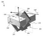
- FIG. 1Ais an isometric schematic diagram showing a backside view of a MEMS element according a first embodiment of the invention
- FIG. 1Bis an isometric schematic diagram showing a frontside view of the MEMS element of FIG. 1A where a moveable element in a first position;
- FIG. 1Cis an isometric schematic diagram showing another frontside view of the MEMS element of FIG. 1A where the moveable element in a second position;
- FIGS. 1D-1Gdepict schematic diagrams of different possible shapes for a portion of the moveable element
- FIGS. 1H-1Ldepict schematic diagrams of different actuation schemes for the moveable element
- FIGS. 1M-1Pdepict schematic diagrams of a MEMS element having a latch
- FIG. 2is an isometric schematic diagram of an optical switch according to a second embodiment of the invention.
- FIG. 3depicts a series of cross sectional diagrams illustrating a method of fabricating a MEMS element according to a third embodiment of the invention
- FIG. 4depicts a series of cross-sectional schematic diagrams illustrating a method of fabricating a MEMS element according to a first alternative version of the third embodiment of the invention.
- a novel MEMS elementhas a vertical plate that can be precisely clamped.
- the platemay be made free of release holes that are common to MEMS mirrors.
- the platemay be made optically flat, and can move or rotate into a substrate.
- the MEMS elementmay be made without requiring long slender hinges, a typical reliability culprit. Another common issue stiction may be reduced significantly also due to a much smaller contact area.
- An array of such MEMScan be easily converted into a planar optical switch fabric for directing optical beams in a communications network.
- This designmay be realized by forming the plate out of a single crystal substrate, e.g., ⁇ 110> silicon with anisotropic etchant.
- the plateis oriented substantially perpendicular to a plane of the substrate.
- the plateis attached to a clamp plate to form a T-beam.
- the mirrorWhen clamped to the substrate, the mirror is at ON position and the clamp plate fixes its angle. This angle will be repeatable from mirror to mirror because all mirrors may be formed by etching the same crystal.
- each platehas the same crystal structure as the substrate.
- the crystal axes of the plateare substantially aligned with the crystal axes of the substrate.
- the MEMS element 100generally includes a substrate 102 and a moveable element 101 ,
- the substrate 102may be a crystalline substrate having a crystal structure characterized by substrate crystal axes 121 , 122 , 123 .
- An example of a suitable single crystalline substrateis silicon.
- the moveable element 101is moveably attached to a first surface 108 of the substrate 102 ; e.g., by a clamping plate 106 and one or more flexures 107 .
- the moveable element 101may be disposed within a slot 105 in the substrate 102 for movement with respect to the substrate 102 .
- the moveable element 101includes a perpendicular portion 104 that is attached to the clamping plate 106 .
- the perpendicular portion 104projects partly beyond a second surface 110 of the substrate 102 .
- the perpendicular portion 104is oriented substantially perpendicular to a plane of the substrate 102 .
- the plane of the substrate 102may be regarded as any plane parallel to the a surface of the substrate 102 , e.g. a plane parallel to the first surface 108 or the second surface 110 .
- the perpendicular portion 104has a crystal structure characterized by moveable element crystal axes 131 , 132 , 133 .
- the perpendicular portion 104may be formed from the substrate 102 such that the crystal structure of the perpendicular portion 104 of the moveable element 101 is substantially the same as the crystal structure of the substrate 102 .
- the moveable element 101is moveable with respect to the substrate 102 between a first position and a second position.
- the motion of the moveable elementis substantially constrained to motion in a plane 111 that is oriented perpendicular to the plane of the substrate 102 .
- the moveable elementmay move between the first and second positions by rotation in the plane 111 , by translation in the plane 111 , or by some combination of rotation and translation within the plane 111 .
- the moveable portionintercepts the path of one or more optical signals 140 .
- a light-deflecting component 113 of the perpendicular portion 104 of the moveable element 101deflects the optical signals 140 .
- the light-deflecting component 113may be a simple plane reflecting (or partially reflecting) coating on the sides of the perpendicular portion 104 .
- the reflective coatingcovers both sides of the perpendicular portion 104 so that the moveable element 101 may reflect optical signals 140 that travel in two different directions.
- the light-deflecting componentmay be curved reflecting (or partially reflecting) surface, prismatic reflector, refractive element, prism, lens, waveguide, diffractive element, e.g. fresnel lens, a dichroic coated surface for wavelength specific and bandpass selectivity, or some combination of these.
- the moveable element 101When the moveable element 101 is in the first position, two or more of the moveable element crystal axes, e.g. axes 131 , 132 , 133 are oriented substantially parallel to two or more corresponding substrate crystal axes, e.g., axes 121 , 122 , 123 .
- the moveable element 101In the second position, depicted in FIG. 1C, the moveable element 101 does not intercept one or more optical signals 140 ′.
- the movable element 101rotates and translates between the first and second positions.
- a slot 105 in the substrate 102receives the perpendicular portion 104 and permits rotation relative to the substrate 102 .
- the moveable element 101may translate between the first and second positions.
- Such translationmay be either parallel to the plane of the substrate 102 or perpendicular to the plane of the substrate 102 . Note that independent of whether the movable element 101 is in the first position, the second position, or some intermediate position, the perpendicular portion 104 always remains substantially perpendicular to the plane of the substrate 102 .
- FIGS. 1D-1Gdepict examples of possible shapes.
- FIG. 1Ddepicts a perpendicular portion 104 D having a substantially rectangular shape.
- FIG. 1Edepicts a perpendicular portion 104 E having a substantially rectangular shape with one or more clipped corners. The corners may be clipped e.g., using an axis-selective etching process.
- FIG. 1Fdepicts a perpendicular portion 104 F having a substantially rectangular shape having arcuate sections removed from one or more corners. The arcuate sections may be formed, e.g. by an isotropic etch process.
- FIG. 1Ddepicts a perpendicular portion 104 D having a substantially rectangular shape.
- FIG. 1Edepicts a perpendicular portion 104 E having a substantially rectangular shape with one or more clipped corners. The corners may be clipped e.g., using an axis-selective etching process.
- FIG. 1Fdepicts a perpendicular
- FIGS. 1E, 1 F and 1 Gdepict a perpendicular portion 104 G having a substantially rectangular shape with one or more rounded corners.
- the shapes of the perpendicular portions depicted in FIGS. 1E, 1 F and 1 Greduce the angular displacement of the respective perpendicular portions 104 E, 104 F and 104 G to translate between the first and second positions.
- MEMS elements of the types depicted abovemay be used in optical switching systems, the present invention is in no way limited to such applications.
- MEMS elements of the types described hereinmay be used in biomedical applications, for example, in microvalves that require precise positioning.
- MEMS elementsmay find application in micro-relays, passive radiofrequency (RF) devices such as tunable capacitors and the like.
- RFradiofrequency
- a magnetic materialmay be deposited onto the clamping plate 106 to allow the moveable element 101 to be driven by external magnetic field.
- another substrate, with electrodesmay be attached to the substrate 102 .
- a voltage applied between the electrodes and the clamping plate 106may produce an electrostatic force that pulls the moveable element.
- These two methodscan use a mechanical restoring torque generated by a torsion hinge as the hinge 107 such that only one-way actuation is required.
- the rotation anglemay be made much smaller than with mirrors formed in the plane of the substrate. Therefore, a stiffer and more robust torsion hinge may be used, which improves device reliability and manufacturability.
- the actuation mechanismmay be incorporated into the flexures 107 .
- the moveable element 101may be actuated with a pre-stressed flexure such as a thermal bimorph actuator or electrostatic actuator.
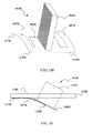
- FIGS. 1H-1Idepict schematic diagrams that illustrate an example of a moveable element 101 H that utilizes pre-stressed flexure.
- the moveable element 101 Hgenerally includes a perpendicular portion 104 H a clamping plate 106 H and a pre-stressed flexure 107 H.
- the pre-stressed flexure 107 His attached at a first end 117 H to a substrate 102 H.
- a second end 119 H of the pre-stressed flexure 107 His free to move.
- the pre-stressed flexure 107 Hmay utilize a bimorph element having two materials with different residual stress.
- the different stress levelsbend the bimorph material causes the second end 119 H of the pre-stressed flexure 107 H to curl away from the substrate 102 H when the second end 119 H is released.
- heatmay be applied to the pre-stressed flexure 107 H (e.g., through a microresistive heater) to pull it and the rest of the moveable element 101 H back toward the substrate 102 H.
- the bimorphcan be built such that the layer next to the substrate 102 H is electrically insulative.
- a voltage applied between the substrate and the other layergenerates an electrostatic force that pulls the moveable element 101 H back toward the substrate 102 H.
- the motion of the moveable element 101 Hmay be described as a combination of translation and rotation with respect to the substrate 102 H.
- a moveable element 101 Jincludes a perpendicular portion 104 J attached to a clamping plate 106 J and one or more elastically deformable flexures 107 J, such as springs, serpentine flexures or polymer flexures.
- the pre-stressed flexures 107 Jare attached to opposite ends of the clamping plate 106 J and to a first surface 108 J of the substrate 102 J. This configuration of pre-stressed flexures 107 J facilitates translation of the moveable element 101 H perpendicular to the substrate 102 J.
- the moveable element 101 Jmay also be actuated under the influence of an electrostatic or magnetic force.
- An electrostatic forcemay be exerted by applying an electric voltage between the clamping plate 106 J and an electrode 112 J.
- the electrode 112 Jmay be disposed on a secondary substrate 116 that is attached to the substrate 102 as shown in FIG. 1K.
- a magnetic forcemay be exerted by applying an external magnetic field to a magnetic material (not shown) attached to the clamping plate 106 J.
- the secondary substrate 116may include a recess 114 that accommodates the movement of the moveable element 101 J and the flexures 107 J.
- a moveable element 101 Lincludes a perpendicular portion 104 L attached to a clamping plate 106 L and one or more torsional hinge flexures 107 L.
- the torsional hinge flexures 107 Lare attached to opposite ends of the clamping plate 106 L and define an axis of rotation.
- the free ends of the torsional hinge flexures 107 Lmay be attached to a substrate such as the substrate 102 of FIGS. 1A-1C.
- the torsional hinge flexures 107 Lapply a torsional, or restoring force that returns the moveable element 101 L to the second position when an actuating force is removed.
- restoring forcesmay be applied to moveable element 101 L to return the flap to the second position.
- Such forcesmay be exerted on moveable element 101 L by biasing mechanisms that operate via electrostatic, pneumatic, thermal, or magnetic principals, including coils that interact with an external magnetic field, electrostatic elements, such as gap closing electrodes, piezoelectric actuators, stress bearing elements and thermal actuators.
- Multiple restoring forcesmay also used together, and the forces may operate along the same or opposing directions.
- FIGS. 1M-1Pdepict a MEMS element 100 M that uses such a latch.
- the MEMS element 100 Mgenerally includes a substrate 102 M a moveable element 101 M and a latch 150 .
- the moveable elementincludes a perpendicular 104 M portion attached to a clamping plate 106 M.
- the clamping pate 106 Mis attached to a first surface 108 M of the substrate 102 M by one or more flexures 107 M.
- the flexures 107 Mmay be any of the types described above.
- the flexures 107 Mpermit the moveable element to move as shown by the curved arrows.
- a part of the perpendicular portion 104 M of the moveable element 101 Mprojects beyond a second surface 110 M of the substrate 102 M.
- the perpendicular elementmay intercept an optical signal 140 M.
- the clamping plate 106 Mis substantially parallel to the first surface of the substrate 102 M and the perpendicular element 104 M is substantially perpendicular to a second surface 110 M of the substrate 102 M.
- the perpendicular elementis moved out of the path of an optical signal 140 M.
- the latch 150retains the moveable element 101 M in the first position.
- the latch 150may include a latch plate 152 , guides 154 A, 154 B, an actuator 156 and one or more optional springs 158 A, 158 B.
- the latch plate 152slides parallel to the substrate 102 M to engage the clamping plate 106 M.
- the guides 154 A, 154 Bconstrain the motion of latch plate 152 to a lateral motion in substantially a single dimension.
- the latch plate 152 and guides 154 A, 154 Bare disposed on a raised portion 151 of the substrate 102 M.
- the latch plate 152may include a stop 160 that restricts the range of the lateral motion of the latch plate 152 .
- the stop 160may be implemented as a projection 153 that engages a slot 155 .
- the projection 153is attached to the raised portion 151 and restricts the lateral motion of the latch plate 152 by engaging either a first end 157 or a second end 159 of the slot 155 .
- FIG. 1Mthe implementation of the stop 160 that is depicted in FIG. 1M is merely one example of many possible stop configurations. Consequently, the invention should not be construed as being limited to this particular configuration.
- the actuator 156provides a force for selectively moving the latch plate 152 into or out of engagement with the clamping plate 106 M.
- the actuator 156may be a magnetic material that interacts with a magnetic field.
- the actuating forcemay alternatively be provided by an actuator operating by electrostatic, pneumatic, piezoelectric, thermal bimorph or other principles.
- the optional springs 158 A, 158 Bmay be attached at one end to the raised portion 151 to urge the latch plate 152 towards the clamping plate 106 M and force the latch plate 152 against the projection 153 .
- the springs 158 A, 158 Bthus provide a restoring force on the latch plate 152 , such that the actuator 156 is only required to exert a force to move the latch out of engagement with the clamping plate 106 M.
- the latch 150is advantageous in MEMS elements that apply an actuating force to move the moveable element 101 M into the first position.
- the latch 150mechanically retains the moveable element 101 M in the first position so that the actuating force may be turned off. This is particularly advantageous if the actuating force involves the use of an electromagnet.
- the electromagnetmay be turned off, and therefore, need not consume power, while the moveable element is retained in the first position by the latch 152 . If the flexure 107 M biases the moveable element in the second position, the electromagnet need only be turned on to move the moveable element 101 M from the second position to the first position. Thus, power consumption may be substantially reduced and the configuration moveable element 101 M may be preserved in the event of a power failure.
- Preserving the state of the moveable element 101 Mis particularly useful where two or more moveable elements are arrayed together in a MEMS device. If each moveable element is provided with a latch, such as the latch 160 , the state of the state of the array, i.e., the set of individual states of each moveable element, may be preserved in the event of a power failure.
- a second embodiment of present inventionincludes systems that incorporate two or more MEMS elements of the type described above with respect to FIGS. 1A-1C, e.g. arranged in an array.
- Such an arrayis depicted in the form of an optical switch 200 of FIG. 2 .
- the optical switch 200generally comprises a crystalline substrate 202 and an array of moveable elements 204 oriented substantially perpendicular to a plane of the substrate 202 .
- the moveable elementshave features in common with MEMS elements the type depicted in FIGS. 1A-1C.
- each element 204has a crystal structure characterized by one or more moveable element crystal axes.
- the crystal structure of each moveable element 204is substantially the same as the crystal structure of the substrate 202 .
- the moveable elements 204include light-deflecting portions that selectively couple optical signals 240 between one or more input fibers 206 and one or more output fibers 208 .
- the moveable elementstranslate perpendicular to a plane of the substrate 202 between a first position and a second position. In the first position, part of a perpendicular portion of a given moveable element projects beyond a surface 210 of the substrate so that the moveable element 204 intercepts the optical signal 240 to deflect it. In the second position, the given moveable element translates into a slot 205 is the substrate 202 to allow the optical signal 240 to bypass without deflection.
- the moveable elements 204 depicted in the optical switch 200 of FIG. 2translate to electively deflect the optical signals 240
- the moveable elementsmay alternatively move in a manner similar to that depicted in any of FIGS. 1B-1P.
- MEMS elementssuch as elements of the types depicted in FIGS. 1A-1P, may be fabricated according to an inventive process.
- a substrateis provided and one or more trenches are formed in the substrate to define a moveable element.
- the moveable elementis moveably attached to a first surface of the substrate. A portion of the substrate is removed such that at least a portion of the moveable element projects beyond a second surface of the substrate.
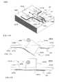
- FIG. 3An example of such a fabrication process is shown in the series of cross-sectional schematic diagrams of FIG. 3 .
- the processstarts at step 301 by forming a clamping plate 306 and one or more flexures 307 on a first surface 323 of a substrate 320 .
- the substrate 320may be a crystalline substrate characterized by a set of substrate crystal axes 322 .
- the clamping plate 306 and flexure 307may be formed from the same material or, alternatively, from different materials.
- a pattern of sacrificial material 308may be deposited prior to forming the clamping plate 306 and flexures 307 .
- the sacrificial materialis deposited on the first surface 323 in a pattern such that the clamping plate 306 and flexures 307 are only attached to the substrate 320 at specific locations.
- step 303one or more trenches 310 are formed in the substrate to define a perpendicular portion 304 of a moveable element.
- the perpendicular portion 304is attached to the substrate 320 by the clamping plate 306 and the flexure 307 . It is important during step 303 to protect the perpendicular portion 304 from being etched by the etch process that forms the trenches 310 in the substrate 320 .
- the perpendicular portion 304 and substrate 320may be protected during this step by a suitably patterned etch-resistant mask (not shown).
- step 305a second surface 325 of the substrate 320 is etched back to expose the perpendicular portion 304 . It is important during step 305 to protect the perpendicular portion from being etched by the etch process that attacks the substrate 320 . Again, a suitable etch-resistant mask may be formed on the perpendicular portion 304 .
- the perpendicular portion 304is oriented substantially perpendicular to a plane of the substrate 320 . Note that the perpendicular portion 304 is formed from the same material as the substrate and need not be rotated out of plane.
- the perpendicular portion 304will be characterized by perpendicular potion crystal axes 342 that substantially align with the substrate crystal axes 322 .
- the perpendicular portion 304may be formed with optically smooth sidewalls.
- the sacrificial material 308may be removed in a final release step to provide one or more gaps 309 between the second surface 323 and the clamping plate 306 and/or flexures 307 .
- the processstarts at step 401 by providing a substrate 422 .
- the substratehas a first surface 424 and a second surface 426 .
- the substrate 422may be a single crystalline base material, characterized by two or more substrate crystal axes 421 , 423 .
- the substrate 422may be a wafer of ⁇ 110> silicon.
- First and second etch resistant insulator material layers 428 , 429are deposited on respectively the first and second surfaces 424 , 426 of the substrate 422 .
- An example of an etch-resistant insulator materialis low stress silicon nitride.
- the etch-resistant insulator materialmay be aluminum nitride or silicon carbide.
- the etch-resistant insulator layer 429may be removed from the second surface 426 and a sacrificial insulator layer 430 may be deposited on the first and second surfaces of the substrate 422 . It is important that the material of sacrificial insulator layer 430 be resistant to an etch process that attacks the bulk material of the substrate 422 .
- An example of a suitable material for the sacrificial insulator layer 430is silicon dioxide, which is resistant to a KOH etch used to etch silicon.
- Steps 401 , 402 and 403illustrate only one example of providing a substrate coated with one or more layers of sacrificial material. There are many other ways of achieving this without departing from the scope of the present invention.
- an etch processopens contact holes 432 through the sacrificial insulation layer 430 on the first surface 424 .
- a second etch processmay form shallow dimples 434 on the surface of the sacrificial insulation layer 430 on the first surface 424 .
- the sacrificial layer 430 on the second surface 426is patterned and etched, e.g. by photolithographic process, in such a way as to leave a strip of sacrificial material 436 right below the contact holes 432 .
- the etch-resistant insulator layer 429is selective to the bulk etch process, it may be possible to pattern the etch-resistant insulator 429 to form the strip 436 shown in step 405 .
- a conductive layer 438is deposited over the sacrificial layer 430 on the first surface 424 of the substrate 422 .
- the conductive layer 438fills the contact holes 432 in the sacrificial insulator layer 430 to attach the conductive layer 432 to the etch-resistant insulator layer 430 on the first surface 424 of the substrate 422 .
- the conductive layer 438also fills the dimples 434 .
- conductive materiale.g. polysilicon
- the deposited conductive materialmay be subsequently stripped from the second surface 426 .
- the conductive materialmay be deposited on only the sacrificial layer 430 on the first surface 424 to form the conductive layer 438 .
- a third etch-resistant insulator layer 440may be deposited on the first surface 424 and a fourth etch-resistant layer 442 may be deposited on the second surface 426 .
- the etch-resistant insulator layer 442 on the second surface 426is patterned, and a through-wafer anisotropic etch forms trenches 444 in the substrate 422 to define a perpendicular potion 446 of a moveable element.
- a layer of sacrificial insulating material 448is formed on the sidewalls of the trenches 444 .
- the substrate 422may be sent to oxidation furnace to form a layer of oxide on the sidewalls of the trenches 444 . It is important that the sacrificial insulator material 448 is resistant to a etch process that etches the material of the substrate 422 .
- the etch-resistant insulator layers 440 , 442are removed from the first and second surfaces 424 , 426 respectively.
- the conductive material 438 on the first surface 424is patterned to form a clamping plate 450 .
- the conductive material 438may also be patterned to form a flexure (not shown) that is attached to the clamping plate 450 .
- An actuatormay also be formed on the clamping plate 450 or other portion of the first surface 424 at this time.
- the bulk material of the substrate 422is etched from the second surface 426 to expose a portion of the perpendicular portion 446 above the second surface 426 of the substrate 422 .
- the substratehas been inverted between steps 411 and 412 .
- the sacrificial insulating material 448 on the sidewalls and the strip of sacrificial material 436protect the sides and end of the perpendicular portion 446 during the etch process. It is critical that the etch process be selective in that it removes the bulk material from substrate 422 but does not attack the sacrificial insulator material in the layer 448 on the sidewalls or the strip 436 .
- a wet etch with KOHmay used.
- a dry etch with XeF 2may be used.
- the remaining sacrificial insulator materialis removed, e.g., the layers 448 on the sidewalls of the moveable element, the strip of sacrificial material 436 on the end of the perpendicular portion 446 and any remaining portions of the sacrificial layer 430 on the first surface 424 of the substrate 422 .
- the perpendicular portion 446 and the clamping plate 450form a moveable element 415 . With the removal of the sacrificial layer 430 , the moveable element 415 is released and free to move.
- the perpendicular portion 446is attached to the susbtrate 422 by the conductive material 450 .
- the filled dimples 434reduce the contact area between the conductive material and the first surface 424 of the substrate 422 , which may help to reduce stiction. Because the perpendicular portion 446 is formed from the substrate 422 , the perpendicular portion 446 has substantially the same crystal structure as the substrate 422 . In particular the perpendicular portion 446 has crystal axes 445 , 447 that align with substrate crystal axes 421 , 423 when the moveable element is in the orientation shown.
- a light-deflective element 452may be formed on the perpendicular portion 446 .
- a light-deflective elementmay be any of the types described above.
- the light-deflective element 452may be a reflective coating, e.g., gold sputter deposited on the perpendicular portion 446 .
- the substrate 422 , with the perpendicular portion 446may be bonded to a handle wafer 454 as shown in step 414 .
- the handle wafer 454can be formed using transparent glass wafers with ITO electrodes to improve ease of inspection.
Landscapes
- Physics & Mathematics (AREA)
- General Physics & Mathematics (AREA)
- Optics & Photonics (AREA)
- Engineering & Computer Science (AREA)
- Computer Hardware Design (AREA)
- Microelectronics & Electronic Packaging (AREA)
- Mechanical Light Control Or Optical Switches (AREA)
- Micromachines (AREA)
Abstract
Description
Claims (6)
Priority Applications (3)
| Application Number | Priority Date | Filing Date | Title |
|---|---|---|---|
| US09/915,217US6583031B2 (en) | 2001-07-25 | 2001-07-25 | Method of making a MEMS element having perpendicular portion formed from substrate |
| PCT/US2002/023672WO2003010878A2 (en) | 2001-07-24 | 2002-07-23 | Mems element having perpendicular portion formed from substrate |
| AU2002326454AAU2002326454A1 (en) | 2001-07-24 | 2002-07-23 | Mems element having perpendicular portion formed from substrate |
Applications Claiming Priority (1)
| Application Number | Priority Date | Filing Date | Title |
|---|---|---|---|
| US09/915,217US6583031B2 (en) | 2001-07-25 | 2001-07-25 | Method of making a MEMS element having perpendicular portion formed from substrate |
Publications (2)
| Publication Number | Publication Date |
|---|---|
| US20030049879A1 US20030049879A1 (en) | 2003-03-13 |
| US6583031B2true US6583031B2 (en) | 2003-06-24 |
Family
ID=25435408
Family Applications (1)
| Application Number | Title | Priority Date | Filing Date |
|---|---|---|---|
| US09/915,217Expired - Fee RelatedUS6583031B2 (en) | 2001-07-24 | 2001-07-25 | Method of making a MEMS element having perpendicular portion formed from substrate |
Country Status (1)
| Country | Link |
|---|---|
| US (1) | US6583031B2 (en) |
Cited By (11)
| Publication number | Priority date | Publication date | Assignee | Title |
|---|---|---|---|---|
| US20030076664A1 (en)* | 2000-04-05 | 2003-04-24 | Milasys Gbr | Micro-functional unit |
| US20030108324A1 (en)* | 2001-12-10 | 2003-06-12 | Jds Uniphase Corporation | Fiber-coupled optical attenuator |
| US6635158B1 (en)* | 2001-07-30 | 2003-10-21 | Glimmerglass Networks, Inc. | Electro ceramic MEMS structure with controlled actuator gap |
| US20040084208A1 (en)* | 2002-10-30 | 2004-05-06 | Ives Thomas W. | Article and method for reducing external excitation of MEMS devices |
| US20040208423A1 (en)* | 2003-04-15 | 2004-10-21 | Motorola, Inc. | Optical path method and apparatus |
| US20050286110A1 (en)* | 2004-06-25 | 2005-12-29 | Industrial Technology Research Institute | MEMS optical switch with self-assembly structure |
| US20090296307A1 (en)* | 2008-06-02 | 2009-12-03 | Fouladi Azarnaminy Siamak | Mems based rf components with vertical motion and parallel-plate structure and manufacture thereof using standard cmos technologies |
| US20100263998A1 (en)* | 2009-04-20 | 2010-10-21 | International Business Machines Corporation | Vertical integrated circuit switches, design structure and methods of fabricating same |
| US20110132088A1 (en)* | 2009-12-04 | 2011-06-09 | The Charles Stark Draper Laboratory, Inc. | Flexure assemblies and methods for manufacturing and using the same |
| US20120127558A1 (en)* | 2010-11-16 | 2012-05-24 | Imec | Diffractive optical nano-electro-mechanical device with reduced driving voltage |
| US8609450B2 (en) | 2010-12-06 | 2013-12-17 | International Business Machines Corporation | MEMS switches and fabrication methods |
Families Citing this family (13)
| Publication number | Priority date | Publication date | Assignee | Title |
|---|---|---|---|---|
| WO2004104673A1 (en)* | 2003-05-26 | 2004-12-02 | Nidec Sankyo Corporation | Optical switch device |
| US7007843B2 (en)* | 2003-06-09 | 2006-03-07 | Symbol Technologies, Inc. | Light beam shaping arrangement and method in electro-optical readers |
| FR2903812B1 (en)* | 2006-07-13 | 2008-10-31 | Commissariat Energie Atomique | INTEGRATED CIRCUIT DISTRIBUTED TO AT LEAST TWO NON-PARALLEL PLANS AND METHOD FOR PRODUCING THE SAME |
| AT513634B1 (en)* | 2012-12-05 | 2015-02-15 | Univ Wien Tech | MEMS sensor for the detection of environmental parameters |
| JP6778134B2 (en)* | 2017-03-14 | 2020-10-28 | 浜松ホトニクス株式会社 | Optical module and its mounting method |
| WO2018168927A1 (en)* | 2017-03-14 | 2018-09-20 | 浜松ホトニクス株式会社 | Light module |
| DE112018001385T5 (en) | 2017-03-14 | 2019-11-28 | Hamamatsu Photonics K.K. | light module |
| WO2018168929A1 (en)* | 2017-03-14 | 2018-09-20 | 浜松ホトニクス株式会社 | Optical module |
| JP6793066B2 (en)* | 2017-03-14 | 2020-12-02 | 浜松ホトニクス株式会社 | Optical module |
| US11513339B2 (en) | 2017-03-14 | 2022-11-29 | Hamamatsu Photonics K.K. | Optical module |
| JP6782651B2 (en)* | 2017-03-14 | 2020-11-11 | 浜松ホトニクス株式会社 | Optical module |
| WO2024206811A1 (en)* | 2023-03-29 | 2024-10-03 | Omnitron Sensors | Locking mechanisms for precision offset/deployment of mems structures |
| US20240327200A1 (en)* | 2023-03-29 | 2024-10-03 | Omnitron Sensors | Locking mechanisms for precision offset/deployment of mems structures |
Citations (32)
| Publication number | Priority date | Publication date | Assignee | Title |
|---|---|---|---|---|
| US5043404A (en) | 1989-04-21 | 1991-08-27 | Xerox Corporation | Semisuspension polymerization processes |
| US5206983A (en) | 1991-06-24 | 1993-05-04 | Wisconsin Alumni Research Foundation | Method of manufacturing micromechanical devices |
| US5314572A (en) | 1990-08-17 | 1994-05-24 | Analog Devices, Inc. | Method for fabricating microstructures |
| EP0605300A1 (en) | 1992-12-28 | 1994-07-06 | Commissariat A L'energie Atomique | Method for manufacturing accelerometers using the silicon on insulator technology and accelerometer thereby obtained |
| US5629918A (en) | 1995-01-20 | 1997-05-13 | The Regents Of The University Of California | Electromagnetically actuated micromachined flap |
| US5637539A (en) | 1996-01-16 | 1997-06-10 | Cornell Research Foundation, Inc. | Vacuum microelectronic devices with multiple planar electrodes |
| US5638946A (en) | 1996-01-11 | 1997-06-17 | Northeastern University | Micromechanical switch with insulated switch contact |
| US5645684A (en) | 1994-03-07 | 1997-07-08 | The Regents Of The University Of California | Multilayer high vertical aspect ratio thin film structures |
| US5717631A (en) | 1995-07-21 | 1998-02-10 | Carnegie Mellon University | Microelectromechanical structure and process of making same |
| US5719073A (en) | 1993-02-04 | 1998-02-17 | Cornell Research Foundation, Inc. | Microstructures and single mask, single-crystal process for fabrication thereof |
| US5770465A (en) | 1995-06-23 | 1998-06-23 | Cornell Research Foundation, Inc. | Trench-filling etch-masking microfabrication technique |
| GB2321780A (en) | 1997-01-31 | 1998-08-05 | Mitsubishi Electric Corp | Sensor element and manufacturting element |
| US5866281A (en) | 1996-11-27 | 1999-02-02 | Wisconsin Alumni Research Foundation | Alignment method for multi-level deep x-ray lithography utilizing alignment holes and posts |
| US5914507A (en) | 1994-05-11 | 1999-06-22 | Regents Of The University Of Minnesota | PZT microdevice |
| US5943155A (en) | 1998-08-12 | 1999-08-24 | Lucent Techonolgies Inc. | Mars optical modulators |
| US5949571A (en) | 1998-07-30 | 1999-09-07 | Lucent Technologies | Mars optical modulators |
| EP0942462A2 (en) | 1998-03-09 | 1999-09-15 | Siemens Aktiengesellschaft | Method and structure for protecting a neighbouring area adjacent to an area to be etched and method for forming a fuse |
| US5960255A (en) | 1994-06-07 | 1999-09-28 | International Business Machines Corporation | Calibration standard for 2-D and 3-D profilometry in the sub-nanometer range and method of producing it |
| US5971355A (en) | 1996-11-27 | 1999-10-26 | Xerox Corporation | Microdevice valve structures to fluid control |
| US6021675A (en) | 1995-06-07 | 2000-02-08 | Ssi Technologies, Inc. | Resonating structure and method for forming the resonating structure |
| US6025951A (en) | 1996-11-27 | 2000-02-15 | National Optics Institute | Light modulating microdevice and method |
| US6074890A (en) | 1998-01-08 | 2000-06-13 | Rockwell Science Center, Llc | Method of fabricating suspended single crystal silicon micro electro mechanical system (MEMS) devices |
| EP1033601A1 (en) | 1999-03-04 | 2000-09-06 | Japan Aviation Electronics Industry, Limited | Optical switch and method of making the same |
| US6121552A (en) | 1997-06-13 | 2000-09-19 | The Regents Of The University Of Caliofornia | Microfabricated high aspect ratio device with an electrical isolation trench |
| WO2000057233A2 (en) | 1999-03-09 | 2000-09-28 | The Regents Of The University Of California | Cantilevered microstructure methods and apparatus |
| US6203715B1 (en) | 1999-01-19 | 2001-03-20 | Daewoo Electronics Co., Ltd. | Method for the manufacture of a thin film actuated mirror array |
| EP1120677A2 (en) | 2000-01-21 | 2001-08-01 | Cronos Integrated Microsystems, Inc. | MEMS optical cross-connect switch |
| US6362512B1 (en)* | 1998-12-23 | 2002-03-26 | Xerox Corporation | Microelectromechanical structures defined from silicon on insulator wafers |
| US6379989B1 (en)* | 1998-12-23 | 2002-04-30 | Xerox Corporation | Process for manufacture of microoptomechanical structures |
| US6389189B1 (en)* | 1998-10-23 | 2002-05-14 | Corning Incorporated | Fluid-encapsulated MEMS optical switch |
| US6404942B1 (en)* | 1998-10-23 | 2002-06-11 | Corning Incorporated | Fluid-encapsulated MEMS optical switch |
| US20020075554A1 (en)* | 2000-07-31 | 2002-06-20 | Brophy Christopher P. | MEMS mirror and method of fabrication |
- 2001
- 2001-07-25USUS09/915,217patent/US6583031B2/ennot_activeExpired - Fee Related
Patent Citations (36)
| Publication number | Priority date | Publication date | Assignee | Title |
|---|---|---|---|---|
| US5043404A (en) | 1989-04-21 | 1991-08-27 | Xerox Corporation | Semisuspension polymerization processes |
| US5314572A (en) | 1990-08-17 | 1994-05-24 | Analog Devices, Inc. | Method for fabricating microstructures |
| US5206983A (en) | 1991-06-24 | 1993-05-04 | Wisconsin Alumni Research Foundation | Method of manufacturing micromechanical devices |
| US5327033A (en) | 1991-06-24 | 1994-07-05 | Wisconsin Alumni Research Foundation | Micromechanical magnetic devices |
| EP0605300A1 (en) | 1992-12-28 | 1994-07-06 | Commissariat A L'energie Atomique | Method for manufacturing accelerometers using the silicon on insulator technology and accelerometer thereby obtained |
| US5576250A (en) | 1992-12-28 | 1996-11-19 | Commissariat A L'energie Atomique | Process for the production of accelerometers using silicon on insulator technology |
| US5780885A (en) | 1992-12-28 | 1998-07-14 | Commissariat A L'energie Atomique | Accelerometers using silicon on insulator technology |
| US5719073A (en) | 1993-02-04 | 1998-02-17 | Cornell Research Foundation, Inc. | Microstructures and single mask, single-crystal process for fabrication thereof |
| US5645684A (en) | 1994-03-07 | 1997-07-08 | The Regents Of The University Of California | Multilayer high vertical aspect ratio thin film structures |
| US5914507A (en) | 1994-05-11 | 1999-06-22 | Regents Of The University Of Minnesota | PZT microdevice |
| US5960255A (en) | 1994-06-07 | 1999-09-28 | International Business Machines Corporation | Calibration standard for 2-D and 3-D profilometry in the sub-nanometer range and method of producing it |
| US5629918A (en) | 1995-01-20 | 1997-05-13 | The Regents Of The University Of California | Electromagnetically actuated micromachined flap |
| US6021675A (en) | 1995-06-07 | 2000-02-08 | Ssi Technologies, Inc. | Resonating structure and method for forming the resonating structure |
| US5770465A (en) | 1995-06-23 | 1998-06-23 | Cornell Research Foundation, Inc. | Trench-filling etch-masking microfabrication technique |
| US5717631A (en) | 1995-07-21 | 1998-02-10 | Carnegie Mellon University | Microelectromechanical structure and process of making same |
| US5638946A (en) | 1996-01-11 | 1997-06-17 | Northeastern University | Micromechanical switch with insulated switch contact |
| US5637539A (en) | 1996-01-16 | 1997-06-10 | Cornell Research Foundation, Inc. | Vacuum microelectronic devices with multiple planar electrodes |
| US5866281A (en) | 1996-11-27 | 1999-02-02 | Wisconsin Alumni Research Foundation | Alignment method for multi-level deep x-ray lithography utilizing alignment holes and posts |
| US5908719A (en) | 1996-11-27 | 1999-06-01 | Wisconsin Alumni Research Foundation | Radiation mask adapted to be aligned with a photoresist layer and method of making the same |
| US5971355A (en) | 1996-11-27 | 1999-10-26 | Xerox Corporation | Microdevice valve structures to fluid control |
| US6025951A (en) | 1996-11-27 | 2000-02-15 | National Optics Institute | Light modulating microdevice and method |
| GB2321780A (en) | 1997-01-31 | 1998-08-05 | Mitsubishi Electric Corp | Sensor element and manufacturting element |
| US6121552A (en) | 1997-06-13 | 2000-09-19 | The Regents Of The University Of Caliofornia | Microfabricated high aspect ratio device with an electrical isolation trench |
| US6074890A (en) | 1998-01-08 | 2000-06-13 | Rockwell Science Center, Llc | Method of fabricating suspended single crystal silicon micro electro mechanical system (MEMS) devices |
| EP0942462A2 (en) | 1998-03-09 | 1999-09-15 | Siemens Aktiengesellschaft | Method and structure for protecting a neighbouring area adjacent to an area to be etched and method for forming a fuse |
| US5949571A (en) | 1998-07-30 | 1999-09-07 | Lucent Technologies | Mars optical modulators |
| US5943155A (en) | 1998-08-12 | 1999-08-24 | Lucent Techonolgies Inc. | Mars optical modulators |
| US6404942B1 (en)* | 1998-10-23 | 2002-06-11 | Corning Incorporated | Fluid-encapsulated MEMS optical switch |
| US6389189B1 (en)* | 1998-10-23 | 2002-05-14 | Corning Incorporated | Fluid-encapsulated MEMS optical switch |
| US6362512B1 (en)* | 1998-12-23 | 2002-03-26 | Xerox Corporation | Microelectromechanical structures defined from silicon on insulator wafers |
| US6379989B1 (en)* | 1998-12-23 | 2002-04-30 | Xerox Corporation | Process for manufacture of microoptomechanical structures |
| US6203715B1 (en) | 1999-01-19 | 2001-03-20 | Daewoo Electronics Co., Ltd. | Method for the manufacture of a thin film actuated mirror array |
| EP1033601A1 (en) | 1999-03-04 | 2000-09-06 | Japan Aviation Electronics Industry, Limited | Optical switch and method of making the same |
| WO2000057233A2 (en) | 1999-03-09 | 2000-09-28 | The Regents Of The University Of California | Cantilevered microstructure methods and apparatus |
| EP1120677A2 (en) | 2000-01-21 | 2001-08-01 | Cronos Integrated Microsystems, Inc. | MEMS optical cross-connect switch |
| US20020075554A1 (en)* | 2000-07-31 | 2002-06-20 | Brophy Christopher P. | MEMS mirror and method of fabrication |
Non-Patent Citations (9)
| Title |
|---|
| Conant et al. "A Flat High Frequency Scanning Micromirror" Abstract Submitted to Hilton Head 2000. |
| Fedder, G.K., "integrated microelectromechanical systems in conventional CMOS", Proceedings of 1997 IEEE International Symposium on Circuits and Systems. Circuits and Systems in the Information Age. ISCAS '97 (Cat. No. 97CH35987), pp. 2821-2824, vol. 4. |
| L. Y. Lin, et al, Free Space Micromachined Optical Switches with Submillisecond Switching Time for Large-Scale Optical Crossconnects, IEEE Photonics Technology Letters, vol. 10, No. 4, Apr. 1998. |
| Marxer et al. "Vertical Mirrors Fabricated by Deep Reactive Ion Etching For Fiber-Optic Switching Applications" Journal of Microelectrcomechanical Systems, vol. 6 No. 3, Sep. 1997. |
| Mita et al., "An Out-of-Plane Polysilicon Actuator With a Smooth Vertical Mirror for Optical Fiber Switch Application". |
| Provisional Patent Application of Behrang Behin et al., "Global Mechanical Stop for Precise Positioning of a Field of Mirrors", filed Mar. 9, 1999. |
| Storment et al. "Flexible Dry Release Process for Aluminum Electrostatic Actuators" Journal of Microelectromechanical System vol. 3 No. 3 Sep. 1994. |
| U.S. pattent application Ser. No. 09/489,264 of Robert L. Wood et al., "MEMS Optical Cross-Connect Switch", filed Jan. 20, 2000. |
| Yao et al., "Single Crystal Silicon Supported Thin Film Micro Mirrors for Optical Applications" Opt. Eng. 36(5) 1408-1413 (May 1997). |
Cited By (21)
| Publication number | Priority date | Publication date | Assignee | Title |
|---|---|---|---|---|
| US20030076664A1 (en)* | 2000-04-05 | 2003-04-24 | Milasys Gbr | Micro-functional unit |
| US7166806B2 (en)* | 2000-04-05 | 2007-01-23 | Milasys Gbr | Micro-functional unit |
| US6635158B1 (en)* | 2001-07-30 | 2003-10-21 | Glimmerglass Networks, Inc. | Electro ceramic MEMS structure with controlled actuator gap |
| US20030108324A1 (en)* | 2001-12-10 | 2003-06-12 | Jds Uniphase Corporation | Fiber-coupled optical attenuator |
| US6807356B2 (en)* | 2001-12-10 | 2004-10-19 | Jds Uniphase Corporation | Fiber-coupled optical attenuator |
| US20040084208A1 (en)* | 2002-10-30 | 2004-05-06 | Ives Thomas W. | Article and method for reducing external excitation of MEMS devices |
| US20040208423A1 (en)* | 2003-04-15 | 2004-10-21 | Motorola, Inc. | Optical path method and apparatus |
| US6891991B2 (en)* | 2003-04-15 | 2005-05-10 | Motorola, Inc. | Optical path method and apparatus |
| US20050286110A1 (en)* | 2004-06-25 | 2005-12-29 | Industrial Technology Research Institute | MEMS optical switch with self-assembly structure |
| US7133185B2 (en) | 2004-06-25 | 2006-11-07 | Industrial Technology Research Institute | MEMS optical switch with self-assembly structure |
| US20090296307A1 (en)* | 2008-06-02 | 2009-12-03 | Fouladi Azarnaminy Siamak | Mems based rf components with vertical motion and parallel-plate structure and manufacture thereof using standard cmos technologies |
| US7858423B2 (en)* | 2008-06-02 | 2010-12-28 | Fouladi Azarnaminy Siamak | MEMS based RF components with vertical motion and parallel-plate structure and manufacture thereof using standard CMOS technologies |
| US20100263998A1 (en)* | 2009-04-20 | 2010-10-21 | International Business Machines Corporation | Vertical integrated circuit switches, design structure and methods of fabricating same |
| US8604898B2 (en) | 2009-04-20 | 2013-12-10 | International Business Machines Corporation | Vertical integrated circuit switches, design structure and methods of fabricating same |
| US8791778B2 (en) | 2009-04-20 | 2014-07-29 | International Business Machines Corporation | Vertical integrated circuit switches, design structure and methods of fabricating same |
| US20110132088A1 (en)* | 2009-12-04 | 2011-06-09 | The Charles Stark Draper Laboratory, Inc. | Flexure assemblies and methods for manufacturing and using the same |
| US8528405B2 (en)* | 2009-12-04 | 2013-09-10 | The Charles Stark Draper Laboratory, Inc. | Flexure assemblies and methods for manufacturing and using the same |
| US20120127558A1 (en)* | 2010-11-16 | 2012-05-24 | Imec | Diffractive optical nano-electro-mechanical device with reduced driving voltage |
| US8643937B2 (en)* | 2010-11-16 | 2014-02-04 | Imec | Diffractive optical nano-electro-mechanical device with reduced driving voltage |
| US8609450B2 (en) | 2010-12-06 | 2013-12-17 | International Business Machines Corporation | MEMS switches and fabrication methods |
| US8829626B2 (en) | 2010-12-06 | 2014-09-09 | International Business Machines Corporation | MEMS switches and fabrication methods |
Also Published As
| Publication number | Publication date |
|---|---|
| US20030049879A1 (en) | 2003-03-13 |
Similar Documents
| Publication | Publication Date | Title |
|---|---|---|
| US6813412B2 (en) | Mems element having perpendicular portion formed from substrate | |
| US6583031B2 (en) | Method of making a MEMS element having perpendicular portion formed from substrate | |
| US6996306B2 (en) | Electrostatically operated micro-optical devices and method for manufacturing thereof | |
| US6735008B2 (en) | MEMS mirror and method of fabrication | |
| US6671078B2 (en) | Electrostatic zipper actuator optical beam switching system and method of operation | |
| US6379510B1 (en) | Method of making a low voltage micro-mirror array light beam switch | |
| KR100451409B1 (en) | Micro-optical switch and method for manufacturing the same | |
| US20020114058A1 (en) | Light-transmissive substrate for an optical MEMS device | |
| US6681063B1 (en) | Low voltage micro-mirror array light beam switch | |
| US6760144B2 (en) | Articulated MEMS electrostatic rotary actuator | |
| EP1130442B1 (en) | Optical switches using dual axis micromirrors | |
| US8691099B2 (en) | Process for fabricating MEMS devices | |
| US20020171327A1 (en) | Microelectromechanical apparatus for elevating and tilting a platform | |
| US6859577B2 (en) | Self assembled micro anti-stiction structure | |
| US7030537B2 (en) | Movable MEMS-based noncontacting device | |
| EP1208403A1 (en) | Microelectromechanical optical switch and method of manufacture thereof | |
| KR20010102533A (en) | Cantilevered microstructure methods and apparatus | |
| US6819820B1 (en) | Use of applied force to improve MEMS switch performance | |
| KR100468853B1 (en) | MEMS comb actuator materialized on insulating material and method of manufacturing thereof | |
| US7945129B2 (en) | Hybrid optical switch apparatus | |
| US6667823B2 (en) | Monolithic in-plane shutter switch | |
| US6556741B1 (en) | MEMS optical switch with torsional hinge and method of fabrication thereof | |
| US20030012545A1 (en) | Broad-band variable optical attenuator | |
| US20020046985A1 (en) | Process for creating an electrically isolated electrode on a sidewall of a cavity in a base | |
| US6771850B1 (en) | Article comprising a MEMS device and method therefor |
Legal Events
| Date | Code | Title | Description |
|---|---|---|---|
| AS | Assignment | Owner name:ONIX MICROSYSTEMS, CALIFORNIA Free format text:ASSIGNMENT OF ASSIGNORS INTEREST;ASSIGNOR:LIN, CHUANG-CHIA;REEL/FRAME:012227/0425 Effective date:20010919 | |
| AS | Assignment | Owner name:DANEMAN, MICHAEL J., CALIFORNIA Free format text:ASSIGNMENT OF ASSIGNORS INTEREST;ASSIGNOR:ONIX MICROSYSTEMS;REEL/FRAME:015141/0620 Effective date:20040401 Owner name:MICHAEL J. DANEMAN, CALIFORNIA Free format text:ASSIGNMENT OF ASSIGNORS INTEREST;ASSIGNOR:ONIX MICROSYSTEMS;REEL/FRAME:015788/0109 Effective date:20040401 | |
| AS | Assignment | Owner name:DANEMAN, MICHAEL J., CALIFORNIA Free format text:CORRECTIV;ASSIGNOR:ONIX MICROSYSTEMS;REEL/FRAME:016513/0223 Effective date:20040401 | |
| FPAY | Fee payment | Year of fee payment:4 | |
| REMI | Maintenance fee reminder mailed | ||
| LAPS | Lapse for failure to pay maintenance fees | ||
| STCH | Information on status: patent discontinuation | Free format text:PATENT EXPIRED DUE TO NONPAYMENT OF MAINTENANCE FEES UNDER 37 CFR 1.362 | |
| FP | Lapsed due to failure to pay maintenance fee | Effective date:20110624 |