US6583028B2 - Methods of forming trench isolation regions - Google Patents
Methods of forming trench isolation regionsDownload PDFInfo
- Publication number
- US6583028B2 US6583028B2US10/209,865US20986502AUS6583028B2US 6583028 B2US6583028 B2US 6583028B2US 20986502 AUS20986502 AUS 20986502AUS 6583028 B2US6583028 B2US 6583028B2
- Authority
- US
- United States
- Prior art keywords
- layer
- trench
- forming
- sidewalls
- insulative material
- Prior art date
- Legal status (The legal status is an assumption and is not a legal conclusion. Google has not performed a legal analysis and makes no representation as to the accuracy of the status listed.)
- Expired - Lifetime
Links
Images


Classifications
- H—ELECTRICITY
- H01—ELECTRIC ELEMENTS
- H01L—SEMICONDUCTOR DEVICES NOT COVERED BY CLASS H10
- H01L21/00—Processes or apparatus adapted for the manufacture or treatment of semiconductor or solid state devices or of parts thereof
- H01L21/70—Manufacture or treatment of devices consisting of a plurality of solid state components formed in or on a common substrate or of parts thereof; Manufacture of integrated circuit devices or of parts thereof
- H01L21/71—Manufacture of specific parts of devices defined in group H01L21/70
- H01L21/76—Making of isolation regions between components
- H01L21/762—Dielectric regions, e.g. EPIC dielectric isolation, LOCOS; Trench refilling techniques, SOI technology, use of channel stoppers
- H01L21/76224—Dielectric regions, e.g. EPIC dielectric isolation, LOCOS; Trench refilling techniques, SOI technology, use of channel stoppers using trench refilling with dielectric materials
Definitions
- Trench isolation regionsare commonly divided into three categories: shallow trenches (STI) (trenches less than about 1 micron deep); moderate depth trenches (trenches of from about 1 to about 3 microns deep); and deep trenches (trenches greater than about 3 microns deep).
- STIshallow trenches
- a dielectric materialis deposited to fill the trenches.
- the widths of the trenchesdecreased until the process of flowing dielectric material into the trenches developed problems.
- a method of forming a trench isolation regionincludes forming a trench within a substrate.
- a silanol layeris formed to partially fill the trench and then at least some of the silanol is converted to a compound comprising at least one of SiO n and RSiO n , where R comprises an organic group.
- An electrically insulative materialis formed over the converted silanol to fill the trench.
- a method of forming a trench isolation regionincludes forming a trench within a substrate.
- a first layer of at least one of Si(OH) x and (CH 3 ) y Si(OH) 4 ⁇ yis formed to partially fill the trench.
- At least some of the Si(OH) x if presentis converted to SiO 2 and at least some of (CH 3 ) y Si(OH) 4 ⁇ y if present is converted to (CH 3 ) x SiO 2-x .
- a layer of an electrically insulative materialis formed to fill the trench.
- a method of forming a trench isolation regionincludes forming a trench within a substrate.
- the trenchhas sidewalls comprising silicon and a base comprising silicon.
- a first electrically insulative layeris formed over the sidewalls and base.
- the first electrically insulative layeris anisotropically etched to expose silicon of the base while leaving silicon of the sidewalls covered.
- a second electrically insulative layeris substantially selectively chemical vapor deposited over the exposed trench base.
- a third electrically insulative layeris formed over the first and second insulative layers to within the trench.
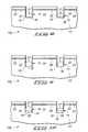
- FIG. 12is a view of the FIG. 8 substrate fragment at a processing step subsequent to that of FIG. 11 .
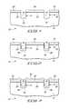
- a semiconductor substrate fragment in processis indicated generally with reference numeral 10 .
- the semiconductor substrate fragment 10comprises the following layers shown in elevationally ascending order: a semiconductor substrate 12 , preferably a bulk monocrystalline silicon substrate; an oxide layer 20 ; and a silicon nitrite layer 22 .
- a series of trenches 14are formed, preferably by an etching process, through layers 20 and 22 and within semiconductor substrate 12 .
- Trench isolation regions 14have sidewalls 16 and base walls 18 .
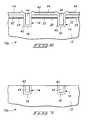
- FIGS. 8-12yet another embodiment in accordance with the invention is described. Like numerals from the previously described embodiments are employed where appropriate, with differences being indicated with a suffix (b) or with different numerals.
- An example chemical vapor deposition processcomprises injecting tetraethylorthosilicate (TEOS) into a reactor chamber at 500 mg/min while flowing O 3 , preferably as a mixture of 12% O 3 and 88% O 2 , at 4000 sccm and helium at from 0-200 sccm and maintaining the substrate 12 at 550° C. and reactor pressure at 200 Torr.
- TEOStetraethylorthosilicate
- planarizationcan be conducted (i.e., chemical-mechanical polishing) to remove layers 30 , 22 , 21 and 20 from over substrate 12 outside of trenches 14 .
- an electrically insulative layer 21is formed over silicon trench sidewalls 16 and trench base 18 by a thermal oxidization process.
- An exemplary method of forming layer 21comprises thermally oxidizing the sidewalls of the trench in an oxidizing environment comprising oxygen and hydrogen and having a greater molar concentration of hydrogen than oxygen.
- first layer 26flows conformably into the trenches during deposition without forming any constrictions at the top of the trenches where voids begin.
- the first layer 26effectively lowers the aspect ratio (defined as trench depth to width) of the trenches preferably by filling at least about a third of the depth while only adding at most 200 angstroms of layer on the sidewalls.
- any subsequent layer deposited to fill the layerwill have a trench with a lower aspect ratio more conducive to filling without voids.
Landscapes
- Engineering & Computer Science (AREA)
- Physics & Mathematics (AREA)
- Condensed Matter Physics & Semiconductors (AREA)
- General Physics & Mathematics (AREA)
- Manufacturing & Machinery (AREA)
- Computer Hardware Design (AREA)
- Microelectronics & Electronic Packaging (AREA)
- Power Engineering (AREA)
- Element Separation (AREA)
Abstract
Description
Claims (23)
Priority Applications (5)
| Application Number | Priority Date | Filing Date | Title |
|---|---|---|---|
| US10/209,865US6583028B2 (en) | 1999-08-30 | 2002-08-02 | Methods of forming trench isolation regions |
| US10/330,881US6719012B2 (en) | 1999-08-30 | 2002-12-23 | Method of forming trench isolation regions |
| US10/688,439US7012010B2 (en) | 1999-08-30 | 2003-10-16 | Methods of forming trench isolation regions |
| US11/170,452US20050239265A1 (en) | 1999-08-30 | 2005-06-29 | Method of forming trench isolation regions |
| US11/170,522US20050239266A1 (en) | 1999-08-30 | 2005-06-29 | Method of forming trench isolation regions |
Applications Claiming Priority (3)
| Application Number | Priority Date | Filing Date | Title |
|---|---|---|---|
| US09/385,915US6300219B1 (en) | 1999-08-30 | 1999-08-30 | Method of forming trench isolation regions |
| US09/900,117US20010041420A1 (en) | 1999-08-30 | 2001-07-06 | Method of forming trench isolation regions |
| US10/209,865US6583028B2 (en) | 1999-08-30 | 2002-08-02 | Methods of forming trench isolation regions |
Related Parent Applications (2)
| Application Number | Title | Priority Date | Filing Date |
|---|---|---|---|
| US09/385,915ContinuationUS6300219B1 (en) | 1999-08-30 | 1999-08-30 | Method of forming trench isolation regions |
| US09/900,117ContinuationUS20010041420A1 (en) | 1999-08-30 | 2001-07-06 | Method of forming trench isolation regions |
Related Child Applications (1)
| Application Number | Title | Priority Date | Filing Date |
|---|---|---|---|
| US10/330,881ContinuationUS6719012B2 (en) | 1999-08-30 | 2002-12-23 | Method of forming trench isolation regions |
Publications (2)
| Publication Number | Publication Date |
|---|---|
| US20020192925A1 US20020192925A1 (en) | 2002-12-19 |
| US6583028B2true US6583028B2 (en) | 2003-06-24 |
Family
ID=23523413
Family Applications (7)
| Application Number | Title | Priority Date | Filing Date |
|---|---|---|---|
| US09/385,915Expired - Fee RelatedUS6300219B1 (en) | 1999-08-30 | 1999-08-30 | Method of forming trench isolation regions |
| US09/900,117AbandonedUS20010041420A1 (en) | 1999-08-30 | 2001-07-06 | Method of forming trench isolation regions |
| US10/209,865Expired - LifetimeUS6583028B2 (en) | 1999-08-30 | 2002-08-02 | Methods of forming trench isolation regions |
| US10/330,881Expired - LifetimeUS6719012B2 (en) | 1999-08-30 | 2002-12-23 | Method of forming trench isolation regions |
| US10/688,439Expired - Fee RelatedUS7012010B2 (en) | 1999-08-30 | 2003-10-16 | Methods of forming trench isolation regions |
| US11/170,452AbandonedUS20050239265A1 (en) | 1999-08-30 | 2005-06-29 | Method of forming trench isolation regions |
| US11/170,522AbandonedUS20050239266A1 (en) | 1999-08-30 | 2005-06-29 | Method of forming trench isolation regions |
Family Applications Before (2)
| Application Number | Title | Priority Date | Filing Date |
|---|---|---|---|
| US09/385,915Expired - Fee RelatedUS6300219B1 (en) | 1999-08-30 | 1999-08-30 | Method of forming trench isolation regions |
| US09/900,117AbandonedUS20010041420A1 (en) | 1999-08-30 | 2001-07-06 | Method of forming trench isolation regions |
Family Applications After (4)
| Application Number | Title | Priority Date | Filing Date |
|---|---|---|---|
| US10/330,881Expired - LifetimeUS6719012B2 (en) | 1999-08-30 | 2002-12-23 | Method of forming trench isolation regions |
| US10/688,439Expired - Fee RelatedUS7012010B2 (en) | 1999-08-30 | 2003-10-16 | Methods of forming trench isolation regions |
| US11/170,452AbandonedUS20050239265A1 (en) | 1999-08-30 | 2005-06-29 | Method of forming trench isolation regions |
| US11/170,522AbandonedUS20050239266A1 (en) | 1999-08-30 | 2005-06-29 | Method of forming trench isolation regions |
Country Status (1)
| Country | Link |
|---|---|
| US (7) | US6300219B1 (en) |
Cited By (11)
| Publication number | Priority date | Publication date | Assignee | Title |
|---|---|---|---|---|
| US20040082181A1 (en)* | 1999-08-30 | 2004-04-29 | Doan Trung Tri | Methods of forming trench isolation regions |
| US20050009368A1 (en)* | 2003-07-07 | 2005-01-13 | Vaartstra Brian A. | Methods of forming a phosphorus doped silicon dioxide comprising layer, and methods of forming trench isolation in the fabrication of integrated circuitry |
| US20050054213A1 (en)* | 2003-09-05 | 2005-03-10 | Derderian Garo J. | Methods of depositing a silicon dioxide comprising layer in the fabrication of integrated circuitry, and methods of forming trench isolation in the fabrication of integrated circuitry |
| US20050208778A1 (en)* | 2004-03-22 | 2005-09-22 | Weimin Li | Methods of depositing silicon dioxide comprising layers in the fabrication of integrated circuitry, methods of forming trench isolation, and methods of forming arrays of memory cells |
| US20050227450A1 (en)* | 2004-04-01 | 2005-10-13 | Derderian Garo J | Methods of forming trench isolation regions |
| US20060046426A1 (en)* | 2004-08-31 | 2006-03-02 | Micron Technology, Inc. | Methods of forming trench isolation in the fabrication of integrated circuitry, methods of fabricating memory circuitry, integrated circuitry and memory integrated circuitry |
| US20060183294A1 (en)* | 2005-02-17 | 2006-08-17 | Micron Technology, Inc. | Methods of forming integrated circuitry |
| US20060197225A1 (en)* | 2005-03-07 | 2006-09-07 | Qi Pan | Electrically conductive line, method of forming an electrically conductive line, and method of reducing titanium silicide agglomeration in fabrication of titanium silicide over polysilicon transistor gate lines |
| US20060223279A1 (en)* | 2005-04-01 | 2006-10-05 | Micron Technology, Inc. | Methods of forming trench isolation in the fabrication of integrated circuitry and methods of fabricating integrated circuitry |
| US20110092061A1 (en)* | 2009-10-20 | 2011-04-21 | Yunjun Ho | Methods of Forming Silicon Oxides and Methods of Forming Interlevel Dielectrics |
| US20240096707A1 (en)* | 2017-09-29 | 2024-03-21 | Taiwan Semiconductor Manufacturing Co., Ltd. | Footing Removal in Cut-Metal Process |
Families Citing this family (87)
| Publication number | Priority date | Publication date | Assignee | Title |
|---|---|---|---|---|
| KR100295782B1 (en)* | 1999-07-03 | 2001-07-12 | 윤종용 | Method for shallow trench isolation |
| US20070014801A1 (en)* | 2001-01-24 | 2007-01-18 | Gish Kurt C | Methods of diagnosis of prostate cancer, compositions and methods of screening for modulators of prostate cancer |
| US6599789B1 (en) | 2000-11-15 | 2003-07-29 | Micron Technology, Inc. | Method of forming a field effect transistor |
| US6897120B2 (en)* | 2001-01-03 | 2005-05-24 | Micron Technology, Inc. | Method of forming integrated circuitry and method of forming shallow trench isolation in a semiconductor substrate |
| US6455382B1 (en)* | 2001-05-03 | 2002-09-24 | Taiwan Semiconductor Manufacturing Co., Ltd. | Multi-step method for forming sacrificial silicon oxide layer |
| US6709930B2 (en)* | 2002-06-21 | 2004-03-23 | Siliconix Incorporated | Thicker oxide formation at the trench bottom by selective oxide deposition |
| US6531377B2 (en)* | 2001-07-13 | 2003-03-11 | Infineon Technologies Ag | Method for high aspect ratio gap fill using sequential HDP-CVD |
| US6596654B1 (en)* | 2001-08-24 | 2003-07-22 | Novellus Systems, Inc. | Gap fill for high aspect ratio structures |
| US6846745B1 (en) | 2001-08-03 | 2005-01-25 | Novellus Systems, Inc. | High-density plasma process for filling high aspect ratio structures |
| US7001854B1 (en) | 2001-08-03 | 2006-02-21 | Novellus Systems, Inc. | Hydrogen-based phosphosilicate glass process for gap fill of high aspect ratio structures |
| KR100428805B1 (en)* | 2001-08-09 | 2004-04-28 | 삼성전자주식회사 | Structure of Trench Isolation and Method of Forming The Same |
| US7067440B1 (en) | 2001-08-24 | 2006-06-27 | Novellus Systems, Inc. | Gap fill for high aspect ratio structures |
| KR100831972B1 (en)* | 2001-12-17 | 2008-05-26 | 주식회사 하이닉스반도체 | Device isolation film formation method of semiconductor device |
| US6716687B2 (en) | 2002-02-11 | 2004-04-06 | Micron Technology, Inc. | FET having epitaxial silicon growth |
| TW536775B (en)* | 2002-04-18 | 2003-06-11 | Nanya Technology Corp | Manufacturing method of shallow trench isolation structure |
| US6716719B2 (en)* | 2002-05-29 | 2004-04-06 | Micron Technology, Inc. | Method of forming biasable isolation regions using epitaxially grown silicon between the isolation regions |
| US7012005B2 (en)* | 2002-06-25 | 2006-03-14 | Siliconix Incorporated | Self-aligned differential oxidation in trenches by ion implantation |
| JP2004047624A (en)* | 2002-07-10 | 2004-02-12 | Renesas Technology Corp | Semiconductor device and method of manufacturing the same |
| US6727150B2 (en) | 2002-07-26 | 2004-04-27 | Micron Technology, Inc. | Methods of forming trench isolation within a semiconductor substrate including, Tshaped trench with spacers |
| US7071043B2 (en)* | 2002-08-15 | 2006-07-04 | Micron Technology, Inc. | Methods of forming a field effect transistor having source/drain material over insulative material |
| US6713365B2 (en)* | 2002-09-04 | 2004-03-30 | Macronix International Co., Ltd. | Methods for filling shallow trench isolations having high aspect ratios |
| DE10249649A1 (en)* | 2002-10-24 | 2004-05-13 | Infineon Technologies Ag | Production of a shallow trench isolation comprises partially filling a recess in a substrate with a filler using a flow-fill process followed by plasma treatment |
| US7122485B1 (en) | 2002-12-09 | 2006-10-17 | Novellus Systems, Inc. | Deposition profile modification through process chemistry |
| US7205248B2 (en)* | 2003-02-04 | 2007-04-17 | Micron Technology, Inc. | Method of eliminating residual carbon from flowable oxide fill |
| US20040248375A1 (en)* | 2003-06-04 | 2004-12-09 | Mcneil John | Trench filling methods |
| US6982207B2 (en)* | 2003-07-11 | 2006-01-03 | Micron Technology, Inc. | Methods for filling high aspect ratio trenches in semiconductor layers |
| US7055912B2 (en)* | 2003-09-23 | 2006-06-06 | Terry Lynn Luscombe | Vehicle mounted utility apparatus with quick attachment means |
| KR100677766B1 (en) | 2003-11-28 | 2007-02-05 | 주식회사 하이닉스반도체 | A semiconductor device having a trench type isolation film and a method of manufacturing the same |
| US7344996B1 (en) | 2005-06-22 | 2008-03-18 | Novellus Systems, Inc. | Helium-based etch process in deposition-etch-deposition gap fill |
| US7163896B1 (en) | 2003-12-10 | 2007-01-16 | Novellus Systems, Inc. | Biased H2 etch process in deposition-etch-deposition gap fill |
| US7476621B1 (en) | 2003-12-10 | 2009-01-13 | Novellus Systems, Inc. | Halogen-free noble gas assisted H2 plasma etch process in deposition-etch-deposition gap fill |
| US7582555B1 (en) | 2005-12-29 | 2009-09-01 | Novellus Systems, Inc. | CVD flowable gap fill |
| US9257302B1 (en) | 2004-03-25 | 2016-02-09 | Novellus Systems, Inc. | CVD flowable gap fill |
| US7074690B1 (en)* | 2004-03-25 | 2006-07-11 | Novellus Systems, Inc. | Selective gap-fill process |
| US7524735B1 (en) | 2004-03-25 | 2009-04-28 | Novellus Systems, Inc | Flowable film dielectric gap fill process |
| US7202185B1 (en) | 2004-06-22 | 2007-04-10 | Novellus Systems, Inc. | Silica thin films produced by rapid surface catalyzed vapor deposition (RVD) using a nucleation layer |
| US7097878B1 (en) | 2004-06-22 | 2006-08-29 | Novellus Systems, Inc. | Mixed alkoxy precursors and methods of their use for rapid vapor deposition of SiO2 films |
| US7129189B1 (en) | 2004-06-22 | 2006-10-31 | Novellus Systems, Inc. | Aluminum phosphate incorporation in silica thin films produced by rapid surface catalyzed vapor deposition (RVD) |
| US7297608B1 (en) | 2004-06-22 | 2007-11-20 | Novellus Systems, Inc. | Method for controlling properties of conformal silica nanolaminates formed by rapid vapor deposition |
| US7217658B1 (en) | 2004-09-07 | 2007-05-15 | Novellus Systems, Inc. | Process modulation to prevent structure erosion during gap fill |
| US7176039B1 (en) | 2004-09-21 | 2007-02-13 | Novellus Systems, Inc. | Dynamic modification of gap fill process characteristics |
| US7148155B1 (en) | 2004-10-26 | 2006-12-12 | Novellus Systems, Inc. | Sequential deposition/anneal film densification method |
| US7790633B1 (en) | 2004-10-26 | 2010-09-07 | Novellus Systems, Inc. | Sequential deposition/anneal film densification method |
| US7381451B1 (en) | 2004-11-17 | 2008-06-03 | Novellus Systems, Inc. | Strain engineering—HDP thin film with tensile stress for FEOL and other applications |
| US7294583B1 (en) | 2004-12-23 | 2007-11-13 | Novellus Systems, Inc. | Methods for the use of alkoxysilanol precursors for vapor deposition of SiO2 films |
| US7223707B1 (en) | 2004-12-30 | 2007-05-29 | Novellus Systems, Inc. | Dynamic rapid vapor deposition process for conformal silica laminates |
| US7271112B1 (en) | 2004-12-30 | 2007-09-18 | Novellus Systems, Inc. | Methods for forming high density, conformal, silica nanolaminate films via pulsed deposition layer in structures of confined geometry |
| US7482247B1 (en) | 2004-12-30 | 2009-01-27 | Novellus Systems, Inc. | Conformal nanolaminate dielectric deposition and etch bag gap fill process |
| US7135418B1 (en) | 2005-03-09 | 2006-11-14 | Novellus Systems, Inc. | Optimal operation of conformal silica deposition reactors |
| US7109129B1 (en) | 2005-03-09 | 2006-09-19 | Novellus Systems, Inc. | Optimal operation of conformal silica deposition reactors |
| US7211525B1 (en) | 2005-03-16 | 2007-05-01 | Novellus Systems, Inc. | Hydrogen treatment enhanced gap fill |
| US7589028B1 (en) | 2005-11-15 | 2009-09-15 | Novellus Systems, Inc. | Hydroxyl bond removal and film densification method for oxide films using microwave post treatment |
| US7491653B1 (en) | 2005-12-23 | 2009-02-17 | Novellus Systems, Inc. | Metal-free catalysts for pulsed deposition layer process for conformal silica laminates |
| US20070194402A1 (en)* | 2006-02-21 | 2007-08-23 | Micron Technology, Inc. | Shallow trench isolation structure |
| US7709345B2 (en)* | 2006-03-07 | 2010-05-04 | Micron Technology, Inc. | Trench isolation implantation |
| US7811935B2 (en)* | 2006-03-07 | 2010-10-12 | Micron Technology, Inc. | Isolation regions and their formation |
| US20070243928A1 (en)* | 2006-04-13 | 2007-10-18 | Igt | Casino gaming incentives using game themes, game types, paytables, denominations |
| US20070246795A1 (en)* | 2006-04-20 | 2007-10-25 | Micron Technology, Inc. | Dual depth shallow trench isolation and methods to form same |
| US7288463B1 (en) | 2006-04-28 | 2007-10-30 | Novellus Systems, Inc. | Pulsed deposition layer gap fill with expansion material |
| US7682977B2 (en)* | 2006-05-11 | 2010-03-23 | Micron Technology, Inc. | Methods of forming trench isolation and methods of forming arrays of FLASH memory cells |
| JP2007335807A (en)* | 2006-06-19 | 2007-12-27 | Toshiba Corp | Manufacturing method of semiconductor device |
| US7482245B1 (en) | 2006-06-20 | 2009-01-27 | Novellus Systems, Inc. | Stress profile modulation in STI gap fill |
| US7625820B1 (en) | 2006-06-21 | 2009-12-01 | Novellus Systems, Inc. | Method of selective coverage of high aspect ratio structures with a conformal film |
| US7888273B1 (en) | 2006-11-01 | 2011-02-15 | Novellus Systems, Inc. | Density gradient-free gap fill |
| US9245739B2 (en) | 2006-11-01 | 2016-01-26 | Lam Research Corporation | Low-K oxide deposition by hydrolysis and condensation |
| DE102006056626B4 (en)* | 2006-11-30 | 2024-12-19 | Advanced Micro Devices, Inc. | Method for forming an opening in a metallization structure of a semiconductor device using a self-limiting deposition process |
| US20080227266A1 (en)* | 2007-03-14 | 2008-09-18 | Texas Instruments Inc. | Method of STI corner rounding using nitridation and high temperature thermal processing |
| US7923373B2 (en) | 2007-06-04 | 2011-04-12 | Micron Technology, Inc. | Pitch multiplication using self-assembling materials |
| US8120137B2 (en)* | 2008-05-08 | 2012-02-21 | Micron Technology, Inc. | Isolation trench structure |
| US8133797B2 (en)* | 2008-05-16 | 2012-03-13 | Novellus Systems, Inc. | Protective layer to enable damage free gap fill |
| US8557712B1 (en) | 2008-12-15 | 2013-10-15 | Novellus Systems, Inc. | PECVD flowable dielectric gap fill |
| US8278224B1 (en) | 2009-09-24 | 2012-10-02 | Novellus Systems, Inc. | Flowable oxide deposition using rapid delivery of process gases |
| WO2011072143A2 (en) | 2009-12-09 | 2011-06-16 | Novellus Systems, Inc. | Novel gap fill integration |
| US8685867B1 (en) | 2010-12-09 | 2014-04-01 | Novellus Systems, Inc. | Premetal dielectric integration process |
| US9719169B2 (en) | 2010-12-20 | 2017-08-01 | Novellus Systems, Inc. | System and apparatus for flowable deposition in semiconductor fabrication |
| EP2495762B1 (en)* | 2011-03-03 | 2017-11-01 | IMEC vzw | Method for producing a floating gate semiconductor memory device |
| US8679940B2 (en)* | 2012-02-17 | 2014-03-25 | GlobalFoundries, Inc. | Methods for fabricating semiconductor devices with isolation regions having uniform stepheights |
| US8846536B2 (en) | 2012-03-05 | 2014-09-30 | Novellus Systems, Inc. | Flowable oxide film with tunable wet etch rate |
| GB201207448D0 (en)* | 2012-04-26 | 2012-06-13 | Spts Technologies Ltd | Method of depositing silicon dioxide films |
| CN103794543B (en)* | 2012-10-31 | 2018-07-10 | 中芯国际集成电路制造(上海)有限公司 | Isolation structure and forming method thereof |
| US9847222B2 (en) | 2013-10-25 | 2017-12-19 | Lam Research Corporation | Treatment for flowable dielectric deposition on substrate surfaces |
| US10049921B2 (en) | 2014-08-20 | 2018-08-14 | Lam Research Corporation | Method for selectively sealing ultra low-k porous dielectric layer using flowable dielectric film formed from vapor phase dielectric precursor |
| US9627246B2 (en)* | 2015-06-10 | 2017-04-18 | Microchip Technology Incorporated | Method of forming shallow trench isolation (STI) structures |
| KR20180069038A (en)* | 2015-11-13 | 2018-06-22 | 어플라이드 머티어리얼스, 인코포레이티드 | Techniques for filling structures using selective surface modification |
| US9916977B2 (en) | 2015-11-16 | 2018-03-13 | Lam Research Corporation | Low k dielectric deposition via UV driven photopolymerization |
| US10388546B2 (en) | 2015-11-16 | 2019-08-20 | Lam Research Corporation | Apparatus for UV flowable dielectric |
| SG11202111547QA (en) | 2019-04-19 | 2021-11-29 | Lam Res Corp | Rapid flush purging during atomic layer deposition |
Citations (26)
| Publication number | Priority date | Publication date | Assignee | Title |
|---|---|---|---|---|
| US3990927A (en) | 1973-11-23 | 1976-11-09 | Commissariat A L'energie Atomique | Method for isolating the components of an integrated circuit |
| US4474975A (en) | 1983-05-09 | 1984-10-02 | The United States Of America As Represented By The Administrator Of The National Aeronautics And Space Administration | Process for producing tris (N-methylamino) methylsilane |
| US5156881A (en) | 1987-03-18 | 1992-10-20 | Kabushiki Kaisha Toshiba | Method for forming a film on a substrate by activating a reactive gas |
| US5182221A (en) | 1990-06-13 | 1993-01-26 | Sony Corporation | Method of filling a recess flat with a material by a bias ECR-CVD process |
| US5410176A (en) | 1991-04-05 | 1995-04-25 | Sgs-Thomson Microelectronics, Inc. | Integrated circuit with planarized shallow trench isolation |
| US5470798A (en) | 1990-05-29 | 1995-11-28 | Mitel Corporation | Moisture-free sog process |
| JPH08146224A (en) | 1994-11-21 | 1996-06-07 | Kyocera Corp | Liquid crystal display |
| US5719085A (en) | 1995-09-29 | 1998-02-17 | Intel Corporation | Shallow trench isolation technique |
| US5741740A (en) | 1997-06-12 | 1998-04-21 | Taiwan Semiconductor Manufacturing Company, Ltd. | Shallow trench isolation (STI) method employing gap filling silicon oxide dielectric layer |
| US5786039A (en) | 1995-05-15 | 1998-07-28 | France Telecom | Process for electrical insulation in microelectronics, applicable in narrow cavities, by deposition of oxide in the viscous state and corresponding device |
| US5801083A (en) | 1997-10-20 | 1998-09-01 | Chartered Semiconductor Manufacturing, Ltd. | Use of polymer spacers for the fabrication of shallow trench isolation regions with rounded top corners |
| US5863827A (en) | 1997-06-03 | 1999-01-26 | Texas Instruments Incorporated | Oxide deglaze before sidewall oxidation of mesa or trench |
| US5883006A (en) | 1997-12-12 | 1999-03-16 | Kabushiki Kaisha Toshiba | Method for making a semiconductor device using a flowable oxide film |
| US5888880A (en) | 1996-10-30 | 1999-03-30 | Advanced Micro Devices, Inc. | Trench transistor with localized source/drain regions implanted through selectively grown oxide layer |
| US5895253A (en) | 1997-08-22 | 1999-04-20 | Micron Technology, Inc. | Trench isolation for CMOS devices |
| US5904540A (en) | 1997-10-18 | 1999-05-18 | United Microelectronics, Corp. | Method for manufacturing shallow trench isolation |
| US5930645A (en) | 1997-12-18 | 1999-07-27 | Advanced Micro Devices, Inc. | Shallow trench isolation formation with reduced polish stop thickness |
| US5943585A (en) | 1997-12-19 | 1999-08-24 | Advanced Micro Devices, Inc. | Trench isolation structure having low K dielectric spacers arranged upon an oxide liner incorporated with nitrogen |
| US5950094A (en) | 1999-02-18 | 1999-09-07 | Taiwan Semiconductor Manufacturing Company, Ltd. | Method for fabricating fully dielectric isolated silicon (FDIS) |
| US5960299A (en) | 1998-10-28 | 1999-09-28 | United Microelectronics Corp. | Method of fabricating a shallow-trench isolation structure in integrated circuit |
| US5972773A (en) | 1995-03-23 | 1999-10-26 | Advanced Micro Devices, Inc. | High quality isolation for high density and high performance integrated circuits |
| US5998280A (en) | 1998-03-20 | 1999-12-07 | National Semiconductor Corporation | Modified recessed locos isolation process for deep sub-micron device processes |
| US6030881A (en) | 1998-05-05 | 2000-02-29 | Novellus Systems, Inc. | High throughput chemical vapor deposition process capable of filling high aspect ratio structures |
| US6051447A (en) | 1997-01-17 | 2000-04-18 | Eastman Kodak Company | Partially pinned photodiode for solid state image sensors |
| US6156674A (en) | 1998-11-25 | 2000-12-05 | Micron Technology, Inc. | Semiconductor processing methods of forming insulative materials |
| US6300219B1 (en) | 1999-08-30 | 2001-10-09 | Micron Technology, Inc. | Method of forming trench isolation regions |
Family Cites Families (56)
| Publication number | Priority date | Publication date | Assignee | Title |
|---|---|---|---|---|
| US112282A (en)* | 1871-02-28 | In sad and fluting irons | ||
| US3809574A (en)* | 1971-07-15 | 1974-05-07 | Rca Corp | Aluminum oxide films for electronic devices |
| US5105253A (en) | 1988-12-28 | 1992-04-14 | Synergy Semiconductor Corporation | Structure for a substrate tap in a bipolar structure |
| JPH02277253A (en) | 1989-04-18 | 1990-11-13 | Mitsubishi Electric Corp | Manufacturing method of semiconductor device |
| JPH0513566A (en) | 1991-07-01 | 1993-01-22 | Toshiba Corp | Manufacture of semiconductor device |
| JP3163719B2 (en) | 1992-01-30 | 2001-05-08 | ソニー株式会社 | Method for manufacturing semiconductor device having polishing step |
| KR950002951B1 (en)* | 1992-06-18 | 1995-03-28 | 현대전자산업 주식회사 | Manufacturing method of trench isolation |
| JPH06334031A (en) | 1993-05-25 | 1994-12-02 | Nec Corp | Element-isolation method for semiconductor device |
| CA2131668C (en)* | 1993-12-23 | 1999-03-02 | Carol Galli | Isolation structure using liquid phase oxide deposition |
| FR2717307B1 (en) | 1994-03-11 | 1996-07-19 | Maryse Paoli | PROCESS FOR ISOLATING ACTIVE ZONES OF A SEMICONDUCTOR SUBSTRATE BY SHALLOW-DEEP NEARLY FLAT SLICES, AND CORRESPONDING DEVICE |
| US5565376A (en)* | 1994-07-12 | 1996-10-15 | United Microelectronics Corp. | Device isolation technology by liquid phase deposition |
| US5895255A (en) | 1994-11-30 | 1999-04-20 | Kabushiki Kaisha Toshiba | Shallow trench isolation formation with deep trench cap |
| US5786263A (en) | 1995-04-04 | 1998-07-28 | Motorola, Inc. | Method for forming a trench isolation structure in an integrated circuit |
| US5616513A (en) | 1995-06-01 | 1997-04-01 | International Business Machines Corporation | Shallow trench isolation with self aligned PSG layer |
| US5518959A (en)* | 1995-08-24 | 1996-05-21 | Taiwan Semiconductor Manufacturing Company | Method for selectively depositing silicon oxide spacer layers |
| KR100209365B1 (en)* | 1995-11-01 | 1999-07-15 | 김영환 | Manufacturing method of S.O.I semiconductor wafer |
| US5770469A (en)* | 1995-12-29 | 1998-06-23 | Lam Research Corporation | Method for forming semiconductor structure using modulation doped silicate glasses |
| US6013583A (en) | 1996-06-25 | 2000-01-11 | International Business Machines Corporation | Low temperature BPSG deposition process |
| US6069055A (en)* | 1996-07-12 | 2000-05-30 | Matsushita Electric Industrial Co., Ltd. | Fabricating method for semiconductor device |
| US5702977A (en)* | 1997-03-03 | 1997-12-30 | Taiwan Semiconductor Manufacturing Company, Ltd. | Shallow trench isolation method employing self-aligned and planarized trench fill dielectric layer |
| TW334614B (en)* | 1997-03-04 | 1998-06-21 | Winbond Electronics Corp | The method of forming shallow trench isolation |
| US5981354A (en) | 1997-03-12 | 1999-11-09 | Advanced Micro Devices, Inc. | Semiconductor fabrication employing a flowable oxide to enhance planarization in a shallow trench isolation process |
| US6097076A (en) | 1997-03-25 | 2000-08-01 | Micron Technology, Inc. | Self-aligned isolation trench |
| US6455394B1 (en)* | 1998-03-13 | 2002-09-24 | Micron Technology, Inc. | Method for trench isolation by selective deposition of low temperature oxide films |
| US7157385B2 (en)* | 2003-09-05 | 2007-01-02 | Micron Technology, Inc. | Method of depositing a silicon dioxide-comprising layer in the fabrication of integrated circuitry |
| US6171962B1 (en) | 1997-12-18 | 2001-01-09 | Advanced Micro Devices, Inc. | Shallow trench isolation formation without planarization mask |
| US6448150B1 (en) | 1998-01-20 | 2002-09-10 | Nanya Technology Corporation | Method for forming shallow trench isolation in the integrated circuit |
| KR100280106B1 (en) | 1998-04-16 | 2001-03-02 | 윤종용 | How to form trench isolation |
| JP3178412B2 (en) | 1998-04-27 | 2001-06-18 | 日本電気株式会社 | Method of forming trench isolation structure |
| US6033961A (en) | 1998-04-30 | 2000-03-07 | Hewlett-Packard Company | Isolation trench fabrication process |
| KR100280107B1 (en) | 1998-05-07 | 2001-03-02 | 윤종용 | How to form trench isolation |
| KR100286736B1 (en) | 1998-06-16 | 2001-04-16 | 윤종용 | How to form trench isolation |
| KR100278657B1 (en) | 1998-06-24 | 2001-02-01 | 윤종용 | Metal line structure for semiconductor device & manufacturing method thereof |
| US5989978A (en) | 1998-07-16 | 1999-11-23 | Chartered Semiconductor Manufacturing, Ltd. | Shallow trench isolation of MOSFETS with reduced corner parasitic currents |
| US6265282B1 (en)* | 1998-08-17 | 2001-07-24 | Micron Technology, Inc. | Process for making an isolation structure |
| TW408432B (en) | 1998-08-25 | 2000-10-11 | United Microelectronics Corp | The manufacture method of shallow trench isolation |
| US5930646A (en)* | 1998-10-09 | 1999-07-27 | Chartered Semiconductor Manufacturing, Ltd. | Method of shallow trench isolation |
| US6090675A (en) | 1999-04-02 | 2000-07-18 | Taiwan Semiconductor Manufacturing Company | Formation of dielectric layer employing high ozone:tetraethyl-ortho-silicate ratios during chemical vapor deposition |
| US6190979B1 (en)* | 1999-07-12 | 2001-02-20 | International Business Machines Corporation | Method for fabricating dual workfunction devices on a semiconductor substrate using counter-doping and gapfill |
| KR20010058498A (en) | 1999-12-30 | 2001-07-06 | 박종섭 | Method of forming trench type isolation layer in semiconductor device |
| US6323104B1 (en) | 2000-03-01 | 2001-11-27 | Micron Technology, Inc. | Method of forming an integrated circuitry isolation trench, method of forming integrated circuitry, and integrated circuitry |
| JP5016767B2 (en) | 2000-03-07 | 2012-09-05 | エーエスエム インターナショナル エヌ.ヴェー. | Method for forming gradient thin film |
| US7011710B2 (en) | 2000-04-10 | 2006-03-14 | Applied Materials Inc. | Concentration profile on demand gas delivery system (individual divert delivery system) |
| US6818250B2 (en) | 2000-06-29 | 2004-11-16 | The Regents Of The University Of Colorado | Method for forming SIO2 by chemical vapor deposition at room temperature |
| KR100815009B1 (en) | 2000-09-28 | 2008-03-18 | 프레지던트 앤드 펠로우즈 오브 하바드 칼리지 | Precipitation Using Vapors of Oxides, Silicates and Phosphates |
| US6617251B1 (en) | 2001-06-19 | 2003-09-09 | Lsi Logic Corporation | Method of shallow trench isolation formation and planarization |
| US6583060B2 (en) | 2001-07-13 | 2003-06-24 | Micron Technology, Inc. | Dual depth trench isolation |
| EP1490529A1 (en)* | 2002-03-28 | 2004-12-29 | President And Fellows Of Harvard College | Vapor deposition of silicon dioxide nanolaminates |
| KR100443126B1 (en)* | 2002-08-19 | 2004-08-04 | 삼성전자주식회사 | trench structure and method of forming thereof |
| GB0220066D0 (en) | 2002-08-29 | 2002-10-09 | Clever Stuff Internat Ltd | Method and device for providing direct access to a particular internet website |
| US6930058B2 (en) | 2003-04-21 | 2005-08-16 | Micron Technology, Inc. | Method of depositing a silicon dioxide comprising layer doped with at least one of P, B and Ge |
| US7282443B2 (en) | 2003-06-26 | 2007-10-16 | Micron Technology, Inc. | Methods of forming metal silicide |
| US7125815B2 (en)* | 2003-07-07 | 2006-10-24 | Micron Technology, Inc. | Methods of forming a phosphorous doped silicon dioxide comprising layer |
| US6933206B2 (en)* | 2003-10-10 | 2005-08-23 | Infineon Technologies Ag | Trench isolation employing a high aspect ratio trench |
| KR100559518B1 (en)* | 2003-12-31 | 2006-03-15 | 동부아남반도체 주식회사 | Formation of STI in Semiconductor |
| US7053010B2 (en)* | 2004-03-22 | 2006-05-30 | Micron Technology, Inc. | Methods of depositing silicon dioxide comprising layers in the fabrication of integrated circuitry, methods of forming trench isolation, and methods of forming arrays of memory cells |
- 1999
- 1999-08-30USUS09/385,915patent/US6300219B1/ennot_activeExpired - Fee Related
- 2001
- 2001-07-06USUS09/900,117patent/US20010041420A1/ennot_activeAbandoned
- 2002
- 2002-08-02USUS10/209,865patent/US6583028B2/ennot_activeExpired - Lifetime
- 2002-12-23USUS10/330,881patent/US6719012B2/ennot_activeExpired - Lifetime
- 2003
- 2003-10-16USUS10/688,439patent/US7012010B2/ennot_activeExpired - Fee Related
- 2005
- 2005-06-29USUS11/170,452patent/US20050239265A1/ennot_activeAbandoned
- 2005-06-29USUS11/170,522patent/US20050239266A1/ennot_activeAbandoned
Patent Citations (27)
| Publication number | Priority date | Publication date | Assignee | Title |
|---|---|---|---|---|
| US3990927A (en) | 1973-11-23 | 1976-11-09 | Commissariat A L'energie Atomique | Method for isolating the components of an integrated circuit |
| US4474975A (en) | 1983-05-09 | 1984-10-02 | The United States Of America As Represented By The Administrator Of The National Aeronautics And Space Administration | Process for producing tris (N-methylamino) methylsilane |
| US5156881A (en) | 1987-03-18 | 1992-10-20 | Kabushiki Kaisha Toshiba | Method for forming a film on a substrate by activating a reactive gas |
| US5776557A (en) | 1987-03-18 | 1998-07-07 | Kabushiki Kaisha Toshiba | Method for forming a film on a substrate by activating a reactive gas |
| US5470798A (en) | 1990-05-29 | 1995-11-28 | Mitel Corporation | Moisture-free sog process |
| US5182221A (en) | 1990-06-13 | 1993-01-26 | Sony Corporation | Method of filling a recess flat with a material by a bias ECR-CVD process |
| US5410176A (en) | 1991-04-05 | 1995-04-25 | Sgs-Thomson Microelectronics, Inc. | Integrated circuit with planarized shallow trench isolation |
| JPH08146224A (en) | 1994-11-21 | 1996-06-07 | Kyocera Corp | Liquid crystal display |
| US5972773A (en) | 1995-03-23 | 1999-10-26 | Advanced Micro Devices, Inc. | High quality isolation for high density and high performance integrated circuits |
| US5786039A (en) | 1995-05-15 | 1998-07-28 | France Telecom | Process for electrical insulation in microelectronics, applicable in narrow cavities, by deposition of oxide in the viscous state and corresponding device |
| US5719085A (en) | 1995-09-29 | 1998-02-17 | Intel Corporation | Shallow trench isolation technique |
| US5888880A (en) | 1996-10-30 | 1999-03-30 | Advanced Micro Devices, Inc. | Trench transistor with localized source/drain regions implanted through selectively grown oxide layer |
| US6051447A (en) | 1997-01-17 | 2000-04-18 | Eastman Kodak Company | Partially pinned photodiode for solid state image sensors |
| US5863827A (en) | 1997-06-03 | 1999-01-26 | Texas Instruments Incorporated | Oxide deglaze before sidewall oxidation of mesa or trench |
| US5741740A (en) | 1997-06-12 | 1998-04-21 | Taiwan Semiconductor Manufacturing Company, Ltd. | Shallow trench isolation (STI) method employing gap filling silicon oxide dielectric layer |
| US5895253A (en) | 1997-08-22 | 1999-04-20 | Micron Technology, Inc. | Trench isolation for CMOS devices |
| US5904540A (en) | 1997-10-18 | 1999-05-18 | United Microelectronics, Corp. | Method for manufacturing shallow trench isolation |
| US5801083A (en) | 1997-10-20 | 1998-09-01 | Chartered Semiconductor Manufacturing, Ltd. | Use of polymer spacers for the fabrication of shallow trench isolation regions with rounded top corners |
| US5883006A (en) | 1997-12-12 | 1999-03-16 | Kabushiki Kaisha Toshiba | Method for making a semiconductor device using a flowable oxide film |
| US5930645A (en) | 1997-12-18 | 1999-07-27 | Advanced Micro Devices, Inc. | Shallow trench isolation formation with reduced polish stop thickness |
| US5943585A (en) | 1997-12-19 | 1999-08-24 | Advanced Micro Devices, Inc. | Trench isolation structure having low K dielectric spacers arranged upon an oxide liner incorporated with nitrogen |
| US5998280A (en) | 1998-03-20 | 1999-12-07 | National Semiconductor Corporation | Modified recessed locos isolation process for deep sub-micron device processes |
| US6030881A (en) | 1998-05-05 | 2000-02-29 | Novellus Systems, Inc. | High throughput chemical vapor deposition process capable of filling high aspect ratio structures |
| US5960299A (en) | 1998-10-28 | 1999-09-28 | United Microelectronics Corp. | Method of fabricating a shallow-trench isolation structure in integrated circuit |
| US6156674A (en) | 1998-11-25 | 2000-12-05 | Micron Technology, Inc. | Semiconductor processing methods of forming insulative materials |
| US5950094A (en) | 1999-02-18 | 1999-09-07 | Taiwan Semiconductor Manufacturing Company, Ltd. | Method for fabricating fully dielectric isolated silicon (FDIS) |
| US6300219B1 (en) | 1999-08-30 | 2001-10-09 | Micron Technology, Inc. | Method of forming trench isolation regions |
Non-Patent Citations (11)
| Title |
|---|
| Beekmann et al., Sub-micron Gap Fill and In-Sutu Planarisation Using Flowfill(TM) Technology, Electrotech, pp. 1-7 (Oct. 1995). |
| Beekmann et al., Sub-micron Gap Fill and In-Sutu Planarisation Using Flowfill™ Technology, Electrotech, pp. 1-7 (Oct. 1995). |
| Horie et al., Kinetics and Mechanism of the Reactions of O(3P) with SiH4, CH3SiH3, (CH3)2SiH2, and (CH3)3SiH, 95 J. Phys. Chem. 4393-4400 (1991). |
| Joshi et al., Plasma Deposited Organosilicon Hydride Network Polymers as Versatile Resists for Entirely Dry Mid-Deep UV Photolithography, 1925 SPIE, 709-720 (Jan. 1993). |
| Kiermasz et al., Planarisation for Sub-Micron Devices Utilising a New Chemistry, 2 pp. (Feb. 1995). |
| Kojima et al., Planarization Procedss Using a Multi-Coating of Spin-on-Glass, IEEE, V-MIC Conf., pp. 390-396 (Jun. 13-14, 1988). |
| Matsuura et al., A Highly Reliable Self-planarizing Low-k Intermetal Dielectric for Sub-quarter Micron Interconnects, IEEE, pp. 785-788 (Jul. 1997). |
| Matsuura et al., Novel Self-planarizing CVD Oxide for Interlayer Dielectric Applications, IEEE, pp. 117-120 (1994). |
| McClatchie et al., Low Dielectric Constant Flowfill(TM) Technology for IMD Applications, 7 pp. (pre-Aug. 1999). |
| McClatchie et al., Low Dielectric Constant Flowfill™ Technology for IMD Applications, 7 pp. (pre-Aug. 1999). |
| Witnall et al. Matrix Reactions of Methylsilanes and Oxygen Atoms, 92 J. Phys. Chem. pp. 594-602 (1988). |
Cited By (50)
| Publication number | Priority date | Publication date | Assignee | Title |
|---|---|---|---|---|
| US7012010B2 (en) | 1999-08-30 | 2006-03-14 | Micron Technology, Inc. | Methods of forming trench isolation regions |
| US20050239266A1 (en)* | 1999-08-30 | 2005-10-27 | Doan Trung T | Method of forming trench isolation regions |
| US20040082181A1 (en)* | 1999-08-30 | 2004-04-29 | Doan Trung Tri | Methods of forming trench isolation regions |
| US7125815B2 (en) | 2003-07-07 | 2006-10-24 | Micron Technology, Inc. | Methods of forming a phosphorous doped silicon dioxide comprising layer |
| US20050124171A1 (en)* | 2003-07-07 | 2005-06-09 | Vaartstra Brian A. | Method of forming trench isolation in the fabrication of integrated circuitry |
| US20070161260A1 (en)* | 2003-07-07 | 2007-07-12 | Vaartstra Brian A | Methods of forming a phosphorus doped silicon dioxide-comprising layer |
| US7790632B2 (en) | 2003-07-07 | 2010-09-07 | Micron Technology, Inc. | Methods of forming a phosphorus doped silicon dioxide-comprising layer |
| US7294556B2 (en) | 2003-07-07 | 2007-11-13 | Micron Technology, Inc. | Method of forming trench isolation in the fabrication of integrated circuitry |
| US20050009368A1 (en)* | 2003-07-07 | 2005-01-13 | Vaartstra Brian A. | Methods of forming a phosphorus doped silicon dioxide comprising layer, and methods of forming trench isolation in the fabrication of integrated circuitry |
| US20060008972A1 (en)* | 2003-09-05 | 2006-01-12 | Derderian Garo J | Method of forming trench isolation in the fabrication of integrated circuitry |
| US7250378B2 (en) | 2003-09-05 | 2007-07-31 | Micron Technology, Inc. | Method of depositing a silicon dioxide-comprising layer in the fabrication of integrated circuitry |
| US7157385B2 (en) | 2003-09-05 | 2007-01-02 | Micron Technology, Inc. | Method of depositing a silicon dioxide-comprising layer in the fabrication of integrated circuitry |
| US20060189158A1 (en)* | 2003-09-05 | 2006-08-24 | Derderian Garo J | Method of depositing a silicon dioxide-comprising layer in the fabrication of integrated circuitry |
| US20050054213A1 (en)* | 2003-09-05 | 2005-03-10 | Derderian Garo J. | Methods of depositing a silicon dioxide comprising layer in the fabrication of integrated circuitry, and methods of forming trench isolation in the fabrication of integrated circuitry |
| US7250380B2 (en) | 2003-09-05 | 2007-07-31 | Micron Technology, Inc. | Method of depositing a silicon dioxide-comprising layer in the fabrication of integrated circuitry |
| US7361614B2 (en) | 2003-09-05 | 2008-04-22 | Micron Technology, Inc. | Method of depositing a silicon dioxide comprising layer in the fabrication of integrated circuitry |
| US20060183347A1 (en)* | 2003-09-05 | 2006-08-17 | Derderian Garo J | Method of depositing a silicon dioxide-comprising layer in the fabrication of integrated circuitry |
| US7429541B2 (en) | 2003-09-05 | 2008-09-30 | Micron Technology, Inc. | Method of forming trench isolation in the fabrication of integrated circuitry |
| US20060189159A1 (en)* | 2003-09-05 | 2006-08-24 | Derderian Garo J | Methods of depositing a silicon dioxide comprising layer in the fabrication of integrated circuitry, and methods of forming trench isolation in the fabrication of integrated circuitry |
| US7053010B2 (en) | 2004-03-22 | 2006-05-30 | Micron Technology, Inc. | Methods of depositing silicon dioxide comprising layers in the fabrication of integrated circuitry, methods of forming trench isolation, and methods of forming arrays of memory cells |
| US20060160375A1 (en)* | 2004-03-22 | 2006-07-20 | Weimin Li | Method of depositing a silicon dioxide-comprising layer in the fabrication of integrated circuitry, methods of forming trench isolation in the fabrication of integrated circuitry, Method of depositing silicon dioxide-comprising layers in the fabrication of integrated circuitry, and methods of forming bit line over capacitor arrays of memory cells |
| US7470635B2 (en) | 2004-03-22 | 2008-12-30 | Micron Technology, Inc. | Method of depositing a silicon dioxide-comprising layer in the fabrication of integrated circuitry, methods of forming trench isolation in the fabrication of integrated circuitry, methods of depositing silicon dioxide-comprising layers in the fabrication of integrated circuitry, and methods of forming bit line over capacitor arrays of memory cells |
| US20050208778A1 (en)* | 2004-03-22 | 2005-09-22 | Weimin Li | Methods of depositing silicon dioxide comprising layers in the fabrication of integrated circuitry, methods of forming trench isolation, and methods of forming arrays of memory cells |
| US7402498B2 (en) | 2004-04-01 | 2008-07-22 | Micron Technology, Inc. | Methods of forming trench isolation regions |
| US7015113B2 (en) | 2004-04-01 | 2006-03-21 | Micron Technology, Inc. | Methods of forming trench isolation regions |
| US20060003543A1 (en)* | 2004-04-01 | 2006-01-05 | Derderian Garo J | Methods of forming trench isolation regions |
| US20060003544A1 (en)* | 2004-04-01 | 2006-01-05 | Derderian Garo J | Methods of forming trench isolation regions |
| US7279396B2 (en) | 2004-04-01 | 2007-10-09 | Micron Technology, Inc. | Methods of forming trench isolation regions with nitride liner |
| US20050227450A1 (en)* | 2004-04-01 | 2005-10-13 | Derderian Garo J | Methods of forming trench isolation regions |
| US20070020881A1 (en)* | 2004-08-31 | 2007-01-25 | Sandhu Gurtej S | Methods of forming trench isolation in the fabrication of integrated circuitry, methods of fabricating memory circuitry, integrated circuitry and memory integrated circuitry |
| US7235459B2 (en) | 2004-08-31 | 2007-06-26 | Micron Technology, Inc. | Methods of forming trench isolation in the fabrication of integrated circuitry, methods of fabricating memory circuitry, integrated circuitry and memory integrated circuitry |
| US20070023856A1 (en)* | 2004-08-31 | 2007-02-01 | Sandhu Gurtej S | Methods of forming trench isolation in the fabrication of integrated circuitry, methods of fabricating memory circuitry, integrated circuitry and memory integrated circuitry |
| US20060046426A1 (en)* | 2004-08-31 | 2006-03-02 | Micron Technology, Inc. | Methods of forming trench isolation in the fabrication of integrated circuitry, methods of fabricating memory circuitry, integrated circuitry and memory integrated circuitry |
| US7364981B2 (en) | 2004-08-31 | 2008-04-29 | Micron Technology, Inc. | Methods of forming trench isolation in the fabrication of integrated circuitry, methods of fabricating memory circuitry, integrated circuitry and memory integrated circuitry |
| US7368800B2 (en) | 2004-08-31 | 2008-05-06 | Micron Technology, Inc. | Methods of forming trench isolation in the fabrication of integrated circuitry, methods of fabricating memory circuitry, integrated circuitry and memory integrated circuitry |
| US7368366B2 (en) | 2004-08-31 | 2008-05-06 | Micron Technology, Inc. | Methods of forming trench isolation in the fabrication of integrated circuitry, methods of fabricating memory circuitry, integrated circuitry and memory integrated circuitry |
| US7387940B2 (en) | 2004-08-31 | 2008-06-17 | Micron Technology, Inc. | Methods of forming trench isolation in the fabrication of integrated circuitry, methods of fabricating memory circuitry, integrated circuitry and memory integrated circuitry |
| US20060046425A1 (en)* | 2004-08-31 | 2006-03-02 | Sandhu Gurtej S | Methods of forming trench isolation in the fabrication of integrated circuitry, methods of fabricating memory circuitry, integrated circuitry and memory integrated circuitry |
| US7217634B2 (en) | 2005-02-17 | 2007-05-15 | Micron Technology, Inc. | Methods of forming integrated circuitry |
| US20060183294A1 (en)* | 2005-02-17 | 2006-08-17 | Micron Technology, Inc. | Methods of forming integrated circuitry |
| US20080284025A1 (en)* | 2005-03-07 | 2008-11-20 | Qi Pan | Electrically Conductive Line |
| US20060197225A1 (en)* | 2005-03-07 | 2006-09-07 | Qi Pan | Electrically conductive line, method of forming an electrically conductive line, and method of reducing titanium silicide agglomeration in fabrication of titanium silicide over polysilicon transistor gate lines |
| US7510966B2 (en) | 2005-03-07 | 2009-03-31 | Micron Technology, Inc. | Electrically conductive line, method of forming an electrically conductive line, and method of reducing titanium silicide agglomeration in fabrication of titanium silicide over polysilicon transistor gate lines |
| US20060223279A1 (en)* | 2005-04-01 | 2006-10-05 | Micron Technology, Inc. | Methods of forming trench isolation in the fabrication of integrated circuitry and methods of fabricating integrated circuitry |
| US8012847B2 (en) | 2005-04-01 | 2011-09-06 | Micron Technology, Inc. | Methods of forming trench isolation in the fabrication of integrated circuitry and methods of fabricating integrated circuitry |
| US8349699B2 (en) | 2005-04-01 | 2013-01-08 | Micron Technology, Inc. | Methods of forming trench isolation in the fabrication of integrated circuitry and methods of fabricating integrated circuitry |
| US20110092061A1 (en)* | 2009-10-20 | 2011-04-21 | Yunjun Ho | Methods of Forming Silicon Oxides and Methods of Forming Interlevel Dielectrics |
| US8105956B2 (en) | 2009-10-20 | 2012-01-31 | Micron Technology, Inc. | Methods of forming silicon oxides and methods of forming interlevel dielectrics |
| US8450218B2 (en) | 2009-10-20 | 2013-05-28 | Micron Technology, Inc. | Methods of forming silicon oxides and methods of forming interlevel dielectrics |
| US20240096707A1 (en)* | 2017-09-29 | 2024-03-21 | Taiwan Semiconductor Manufacturing Co., Ltd. | Footing Removal in Cut-Metal Process |
Also Published As
| Publication number | Publication date |
|---|---|
| US7012010B2 (en) | 2006-03-14 |
| US20010041420A1 (en) | 2001-11-15 |
| US20050239266A1 (en) | 2005-10-27 |
| US6719012B2 (en) | 2004-04-13 |
| US20020192925A1 (en) | 2002-12-19 |
| US20030092241A1 (en) | 2003-05-15 |
| US20040082181A1 (en) | 2004-04-29 |
| US20050239265A1 (en) | 2005-10-27 |
| US6300219B1 (en) | 2001-10-09 |
Similar Documents
| Publication | Publication Date | Title |
|---|---|---|
| US6583028B2 (en) | Methods of forming trench isolation regions | |
| KR100788183B1 (en) | Ozone post-deposition treatment to remove carbon in a flowable oxide film | |
| KR100536604B1 (en) | Method of gap-fill using a high density plasma deposision | |
| US6271153B1 (en) | Semiconductor processing method and trench isolation method | |
| US20040212036A1 (en) | Method of eliminating residual carbon from flowable oxide fill | |
| US6809004B2 (en) | Method of forming a shallow trench isolation | |
| US5981402A (en) | Method of fabricating shallow trench isolation | |
| KR100418475B1 (en) | Method For Shallow Trench Isolation Of Semiconductor Devices | |
| KR100295782B1 (en) | Method for shallow trench isolation | |
| KR100477810B1 (en) | Fabricating method of semiconductor device adopting nf3 high density plasma oxide layer | |
| US6737328B1 (en) | Methods of forming silicon dioxide layers, and methods of forming trench isolation regions | |
| US6548426B1 (en) | Method for improving a quality of dielectric layer and semiconductor device | |
| KR100555472B1 (en) | Trench device isolation using selective epitaxial growth | |
| US6861333B2 (en) | Method of reducing trench aspect ratio | |
| KR100335264B1 (en) | Device Separation Method of Semiconductor Device | |
| KR100568849B1 (en) | Manufacturing method of semiconductor device | |
| KR20020010816A (en) | Method of forming contact in semiconductor device | |
| KR100379524B1 (en) | Method for forming isolation layer in the semiconductor device | |
| KR100538809B1 (en) | Fabricating method of isolation layer adopting nf3 high density plasma oxide layer | |
| KR20010025923A (en) | Method for shallow trench isolation | |
| KR20010109544A (en) | Method for forming isolation layer of semiconductor device | |
| KR20020002161A (en) | Method for forming isolation layer of semiconductor device | |
| KR20050003009A (en) | Method for forming trench type isolation layer in semiconductor device | |
| KR20080002505A (en) | Device Separating Method of Semiconductor Device |
Legal Events
| Date | Code | Title | Description |
|---|---|---|---|
| STCF | Information on status: patent grant | Free format text:PATENTED CASE | |
| CC | Certificate of correction | ||
| FEPP | Fee payment procedure | Free format text:PAYOR NUMBER ASSIGNED (ORIGINAL EVENT CODE: ASPN); ENTITY STATUS OF PATENT OWNER: LARGE ENTITY | |
| FPAY | Fee payment | Year of fee payment:4 | |
| FPAY | Fee payment | Year of fee payment:8 | |
| FPAY | Fee payment | Year of fee payment:12 | |
| AS | Assignment | Owner name:U.S. BANK NATIONAL ASSOCIATION, AS COLLATERAL AGENT, CALIFORNIA Free format text:SECURITY INTEREST;ASSIGNOR:MICRON TECHNOLOGY, INC.;REEL/FRAME:038669/0001 Effective date:20160426 Owner name:U.S. BANK NATIONAL ASSOCIATION, AS COLLATERAL AGEN Free format text:SECURITY INTEREST;ASSIGNOR:MICRON TECHNOLOGY, INC.;REEL/FRAME:038669/0001 Effective date:20160426 | |
| AS | Assignment | Owner name:MORGAN STANLEY SENIOR FUNDING, INC., AS COLLATERAL AGENT, MARYLAND Free format text:PATENT SECURITY AGREEMENT;ASSIGNOR:MICRON TECHNOLOGY, INC.;REEL/FRAME:038954/0001 Effective date:20160426 Owner name:MORGAN STANLEY SENIOR FUNDING, INC., AS COLLATERAL Free format text:PATENT SECURITY AGREEMENT;ASSIGNOR:MICRON TECHNOLOGY, INC.;REEL/FRAME:038954/0001 Effective date:20160426 | |
| AS | Assignment | Owner name:U.S. BANK NATIONAL ASSOCIATION, AS COLLATERAL AGENT, CALIFORNIA Free format text:CORRECTIVE ASSIGNMENT TO CORRECT THE REPLACE ERRONEOUSLY FILED PATENT #7358718 WITH THE CORRECT PATENT #7358178 PREVIOUSLY RECORDED ON REEL 038669 FRAME 0001. ASSIGNOR(S) HEREBY CONFIRMS THE SECURITY INTEREST;ASSIGNOR:MICRON TECHNOLOGY, INC.;REEL/FRAME:043079/0001 Effective date:20160426 Owner name:U.S. BANK NATIONAL ASSOCIATION, AS COLLATERAL AGEN Free format text:CORRECTIVE ASSIGNMENT TO CORRECT THE REPLACE ERRONEOUSLY FILED PATENT #7358718 WITH THE CORRECT PATENT #7358178 PREVIOUSLY RECORDED ON REEL 038669 FRAME 0001. ASSIGNOR(S) HEREBY CONFIRMS THE SECURITY INTEREST;ASSIGNOR:MICRON TECHNOLOGY, INC.;REEL/FRAME:043079/0001 Effective date:20160426 | |
| AS | Assignment | Owner name:JPMORGAN CHASE BANK, N.A., AS COLLATERAL AGENT, ILLINOIS Free format text:SECURITY INTEREST;ASSIGNORS:MICRON TECHNOLOGY, INC.;MICRON SEMICONDUCTOR PRODUCTS, INC.;REEL/FRAME:047540/0001 Effective date:20180703 Owner name:JPMORGAN CHASE BANK, N.A., AS COLLATERAL AGENT, IL Free format text:SECURITY INTEREST;ASSIGNORS:MICRON TECHNOLOGY, INC.;MICRON SEMICONDUCTOR PRODUCTS, INC.;REEL/FRAME:047540/0001 Effective date:20180703 | |
| AS | Assignment | Owner name:MICRON TECHNOLOGY, INC., IDAHO Free format text:RELEASE BY SECURED PARTY;ASSIGNOR:U.S. BANK NATIONAL ASSOCIATION, AS COLLATERAL AGENT;REEL/FRAME:047243/0001 Effective date:20180629 | |
| AS | Assignment | Owner name:MICRON TECHNOLOGY, INC., IDAHO Free format text:RELEASE BY SECURED PARTY;ASSIGNOR:MORGAN STANLEY SENIOR FUNDING, INC., AS COLLATERAL AGENT;REEL/FRAME:050937/0001 Effective date:20190731 | |
| AS | Assignment | Owner name:MICRON TECHNOLOGY, INC., IDAHO Free format text:RELEASE BY SECURED PARTY;ASSIGNOR:JPMORGAN CHASE BANK, N.A., AS COLLATERAL AGENT;REEL/FRAME:051028/0001 Effective date:20190731 Owner name:MICRON SEMICONDUCTOR PRODUCTS, INC., IDAHO Free format text:RELEASE BY SECURED PARTY;ASSIGNOR:JPMORGAN CHASE BANK, N.A., AS COLLATERAL AGENT;REEL/FRAME:051028/0001 Effective date:20190731 |