US6582987B2 - Method of fabricating microchannel array structure embedded in silicon substrate - Google Patents
Method of fabricating microchannel array structure embedded in silicon substrateDownload PDFInfo
- Publication number
- US6582987B2 US6582987B2US10/022,093US2209301AUS6582987B2US 6582987 B2US6582987 B2US 6582987B2US 2209301 AUS2209301 AUS 2209301AUS 6582987 B2US6582987 B2US 6582987B2
- Authority
- US
- United States
- Prior art keywords
- microchannel
- array structure
- microchannel array
- micro
- substrate
- Prior art date
- Legal status (The legal status is an assumption and is not a legal conclusion. Google has not performed a legal analysis and makes no representation as to the accuracy of the status listed.)
- Expired - Lifetime
Links
Images


Classifications
- B—PERFORMING OPERATIONS; TRANSPORTING
- B81—MICROSTRUCTURAL TECHNOLOGY
- B81C—PROCESSES OR APPARATUS SPECIALLY ADAPTED FOR THE MANUFACTURE OR TREATMENT OF MICROSTRUCTURAL DEVICES OR SYSTEMS
- B81C1/00—Manufacture or treatment of devices or systems in or on a substrate
- B81C1/00015—Manufacture or treatment of devices or systems in or on a substrate for manufacturing microsystems
- B81C1/00023—Manufacture or treatment of devices or systems in or on a substrate for manufacturing microsystems without movable or flexible elements
- B81C1/00119—Arrangement of basic structures like cavities or channels, e.g. suitable for microfluidic systems
- B—PERFORMING OPERATIONS; TRANSPORTING
- B81—MICROSTRUCTURAL TECHNOLOGY
- B81B—MICROSTRUCTURAL DEVICES OR SYSTEMS, e.g. MICROMECHANICAL DEVICES
- B81B2201/00—Specific applications of microelectromechanical systems
- B81B2201/02—Sensors
- B81B2201/0214—Biosensors; Chemical sensors
- B—PERFORMING OPERATIONS; TRANSPORTING
- B81—MICROSTRUCTURAL TECHNOLOGY
- B81B—MICROSTRUCTURAL DEVICES OR SYSTEMS, e.g. MICROMECHANICAL DEVICES
- B81B2201/00—Specific applications of microelectromechanical systems
- B81B2201/05—Microfluidics
- B81B2201/058—Microfluidics not provided for in B81B2201/051 - B81B2201/054
Definitions
- the present inventionrelates to a microchannel array structure embedded in a silicon substrate and a fabrication method thereof; and, more particularly, to a structure of high-density ultra fine microchannel array buried deep in a silicon substrate by silicon surface micromachining using semiconductor batch processing.
- the MEMS technologyis expanding its applicable range day by day up to RLC passive components, RF and microwave devices, flat panel displays and core optical components for telecommunication, as highly integrated semiconductor technology deploys.
- RLC passive componentspassive components
- RF and microwave devicesflat panel displays
- core optical componentsfor telecommunication
- microfluidic MEMSfluidic MEMS technologies
- a lab-on-a-chipwhich is being developed as a microfluidic platform for systemizing and integrating bio-chips such as DNA chips, protein chips, immuno-assays and the like.
- bio-chipssuch as DNA chips, protein chips, immuno-assays and the like.
- These devicesare formed based on a plurality of microchannel structures such as microfluidic networks, as they conduct functions of separation, extraction, filtration, mixing and transport of reagents, liquids, or minute particles, making use of the principle of electrophoresis or dielectrophoresis with the aid of microcelectrodes.
- additional high-performance micro heatersare required for the embodiment of micro PCR (polymerase chain reaction) amplifiers, micro reactors and so forth.
- Microchannel structuresare used to interconnect microfluidic components, e.g., micro pumps, micro valves, micro sensors in micro total analysis systems, drug delivery systems, HPLC (high performance liquid chromatography), etc., or used as separation columns as well as heat sinks and heat exchangers that cool down electronic components such as CPUs, infrared sensors, high power semiconductor lasers.
- microfluidic componentse.g., micro pumps, micro valves, micro sensors in micro total analysis systems, drug delivery systems, HPLC (high performance liquid chromatography), etc.
- HPLChigh performance liquid chromatography
- Microchannel structuresare used to interconnect microfluidic components, e.g., micro pumps, micro valves, micro sensors in micro total analysis systems, drug delivery systems, HPLC (high performance liquid chromatography), etc., or used as separation columns as well as heat sinks and heat exchangers that cool down electronic components such as CPUs, infrared sensors, high power semiconductor lasers.
- Microchannels with as many uses as mentioned aboveare usually fabricated by bulk micromachining, polymer-based micromachining, or surface micromachining.
- the bulk micromachining methodmainly focuses on bonding and wet etching of a substrate itself, while surface micromachining features a technique of deposition or dry etching of thin layers on the top of a substrate.
- microchannelsare fabricated by locally processing a silicon, glass or quartz substrate with an etching solution, dry etching, or laser cutting, forming channel patterns, and is hermetically sealed by attaching another substrate thereto by anodic or fusion bonding, diffusion bonding or soldering.
- Another method of making microchannelsare to form channel patterns by coating a thick polymer layer on the top of a substrate; radiating it with UV light; attaching another substrate to the top of the channels, or coating a polymer layer again on the formed channel patterns; then doing patterning of etch holes; and then removing the sacrificial polymer layer below the final polymer layer.
- a microchannelcan be fabricated by using a sacrificial oxide or photoresist layer.
- the sacrificial layeris filled up in the region where channels will be formed.
- a microchannel outer wallis deposited or electroplated on the top of the sacrificial layer, and then the sacrificial layer is removed by an etching solution. It's also possible to make microchannels by patterning a thin masking film in slot shapes on the top of a substrate, anisotropically etching the substrate with an etching solution, thus forming channel patterns. Then, a thin layer is deposited on the entrances to hermetically seal up the channels.
- the conventional methods seen abovehave problems of generating pores on the interface, so they are not appropriate to be applied to the fabrication of ultra fine microchannels whose width is less than tens of ⁇ m, because it's hard to control the channel size.
- the manufacturing processis complex with narrow choice in selecting channel materials. Also, it's hard to form such additional structures as micro sensors, micro actuators, passive elements and electronic devices on the top of a substrate.
- the channelhas a limitation on its height, thereby affecting the following step of photolithography, because it's difficult to deposit the sacrificial layer thick more than a few ⁇ m in CMOS semiconductor processes.
- the problem of the conventional method in forming channels inside a substrateis that the channel shape depends on the etching rate of the substrate you choose, and the width of channels is relatively as big as tens of ⁇ m.
- an object of the present inventionto provide a high-density ultra fine microchannel array structure embedded in a silicon substrate with a channel whose size is as fine as less than tens of ⁇ m, preferably less than a few ⁇ m, and a fabrication method thereof.
- the present inventionprovides a high-density ultra fine microchannel array structure with a planar surface embedded in a silicon substrate by surface micromachining using semiconductor batch processing, and a method of integrating a high-performance micro heater or a micro electrode integrated on the top of the microchannel array structure.
- a method of fabricating a microchannel array structurefurther including the steps of: a) forming a micro heater or a micro electrode by locally doping impurities into the top surface of the microchannel outer wall, or by depositing and etching an additional thin layer on the outer wall after the microchannel outer wall is formed; and b) forming electrical pads by depositing and etching a metal layer on the micro heater or the micro electrode.
- a microchannel arrayformed with a plurality of microchannels, of which the planar structure shapes like a slot or an isolated column, and cross-sections of which shape like squares, rounds, hemicycles, lozenges, trapezoids, triangles, hexagon and so forth.
- a microchannel arrayformed with highly integrated ultra fine microchannels whose sectional width, or diameter, is 10 ⁇ 1 ⁇ 10 0 ⁇ m long.
- a microchannel array regionhas a sectional width, or diameter, of 10 0 ⁇ 10 3 ⁇ m.
- a microchannel outer wallformed out of polysilicon, amorphous or single-crystal silicon, conductors, insulators, or semiconductors.
- a micro heaterformed out of polysilicon, amorphous or single-crystal silicon layers, conducting layers, or semiconductor layers, otherwise, there is provided a micro electrode formed out of polysilicons, amorphous or single-crystal silicon layers, conducting layers, or semiconductor layers.
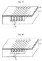
- FIGS. 1A to 1 Ddepict microchannel array structures in accordance with an embodiment of the present invention
- FIGS. 2A to 2 Ishow cross-sectional views illustrating the fabrication method of a microchannel array structure in accordance with an embodiment of the present invention.
- FIG. 3is a photograph of a scanning electron micrograph of a cross-section of a microchannel array structure in accordance with the embodiment of the present invention.
- FIGS. 1A to 1 Dare schematics of a microchannel array structure which a micro heater or a micro electrode is integrated into in accordance with an embodiment of the present invention.
- the microchannel array structure of the present inventionis fabricated by surface micromachining using CMOS semiconductor fabrication processes. Largely, the microchannel array structure has five sections: silicon substrates 101 , 201 , 301 ; microchannel arrays embedded therein 102 , 202 , 302 ; microchannel outer walls 103 , 203 , 303 ; a micro heater or a micro electrode 104 , 214 ; and electrical pads 105 , 215 .
- FIGS. 2A to 2 Iare cross-sectional views illustrating the method of fabricating a microchannel array structure in accordance with a preferred embodiment of the present invention.
- the whole processstarts with a silicon wafer using one or three pieces of pattern masks, followed by the steps of forming silicon trench structures and trench thermal oxide layers, an outer wall and a heater or an electrode, then removing a sacrificial layer, and then forming pads for electric interconnection.
- FIG. 2the embodiment of the present invention is described in detail, hereinafter.
- a five-inch and p-type silicon waferis used as a substrate after going through the standard cleaning method, then a silicon nitride layer (Si 3 N 4 ) (1000 ⁇ 2000 ⁇ ) 204 and a silicon oxide layer (SiO 2 ) (1000 ⁇ 8000 ⁇ ) 205 are deposited for masking, are grown up sequentially by being treated with LPCVD (low pressure chemical vapor deposition) or PECVD (plasma enhanced chemical vapor deposition). And then, a photoresist (PR) layer 206 is coated and exposed to UV light using a first mask, patterned and defined with a plurality of fine lines and spaces.
- LPCVDlow pressure chemical vapor deposition
- PECVDplasma enhanced chemical vapor deposition
- the PR 206is removed after the masking layers of SiO 2 205 and Si 3 N 4 204 for forming silicon trenches are dry-etched.
- the exposed silicon substrate 101 , 201 , 301is dry-etched 10 ⁇ 1 ⁇ 10 2 ⁇ m deep by reactive ion etching (RIE) or deep-RIE, so that silicon trench structures 208 are formed. It's advisable to set the x:y ratio of a line to a space at 0.45:>0.55, because it will form a micropore portion 211 between the trench thermal oxide layers 209 generated from silicon oxidation in the later procedure as shown in FIG. 2 C.
- RIEreactive ion etching
- the shape of trench structures formed in the silicon substrateis not limited to the shape of lines and spaces, but it's possible to etch in any shapes, the planar structure of which shapes like slots or isolated columns, and cross-section of which shapes like polygons such as, squares, rounds, hemicycles, lozenges, trapezoids, triangles, hexagon and so forth.
- the silicon substrate 101 , 201 , 301is doped into n-type with POCl 3 diffusion in a furnace at a temperature of 900° C. for 30 minutes. This procedure is meant to accelerate the thermal oxidation of the silicon trench structures 208 and to remove the P-containing trench thermal oxide layer 209 easily by HF etching during the steps of FIGS. 2C and 2F or 2 I.
- FIG. 2Cshows procedures of removing the SiO 2 layer 205 with BHF solution, thermally oxidizing a plurality of n + -doped silicon trench structures 208 in a furnace filled with O 2 or H 2 /O 2 at a temperature of 900 ⁇ 1000° C., then converting them into trench thermal oxide layers 209 , using the Si 3 N 4 layer 204 as an oxidation mask. Then define a microchannel array formation region 210 , of which the size is 10 0 ⁇ 10 3 ⁇ m in a sectional width or diameter.
- the micropore portion 211whose width is variable between 0.2 ⁇ 1 ⁇ m according to the design condition, are formed simultaneously between the trench thermal oxide layers 209 , the sacrificial layers.
- the trench thermal oxide layers 209 right below the micropore portion 211are removed by dry-etching until the micropore portion 211 reaches the silicon substrates 101 , 201 , 301 , and then the Si 3 N 4 layer 204 is removed with H 3 PO 4 solution.
- FIG. 2Eshows a polysilicon layer 103 , 203 , 303 which can be deposited over 0.4 ⁇ m-thick, more preferably over 1 ⁇ m-thick, by the LPCVD or PECVD technique according to the design condition.
- the polysilicon layerfills the micropore portion 211 regularly arrayed in the silicon substrate, thereby forming a microchannel outer wall 103 , 203 , 303 .
- the compression stress within the polysilicon layershould be relieved by being heated it in a furnace filled with N 2 at 1000° C. for two hours.
- the material for the microchannel outer wallis not confined to the polysilicon layer alone but other various thin films such as conducting layers, insulating ones, or semiconductor layers are available.
- the trench thermal oxide layers 209 in the microchannel array formation region 210can be removed either by wet etching using HF solution or gas-phase etching using anhydrous HF.
- etching the sacrificial layer as abovea plurality of microchannels embedded in the silicon substrate can be formed and the upper part of it gets to have a planar structure.
- the step of FIG. 2Eshould be directly followed by the steps of FIGS. 2G to 2 I with the step of FIG. 2F being skipped.
- a Si 3 N 4 or SiO 2 insulating layer 212should be deposited for masking in a method of either LPCVD or PECVD prior to the PR 213 , and then patterned by using a second mask, before the microchannel array is formed by etching out the sacrificial layer.
- the microchannel outer wall, the polysilicon layers 103 , 203 , 303is thermally treated after being locally doped with ion implant or furnace diffusion.
- n + or p + -doped polysilicon section 104 , 214becomes a buried heater 104 , 214 by forming a diffused resistor.
- This material for a heateris not confined to the polysilicon layer.
- the heatercan be formed by taking the patterning step after the deposition of an insulation layer 212 in FIG. 2G, and going into the procedure of depositing a number of conducting or semiconductor layers and then doing patterning.
- An electrodecan be formed in the same way.
- microchannel arrays 102 , 202 , 302 respectively embedded in the silicon substrate 101 , 201 , 301is formed through the procedure of removing a plurality of trench thermal oxide layers 209 in the microchannel array formation region 210 by HF wet etching or gas-phase etching.
- the next stepis to deposit a metal layer by sputtering or e-beam evaporation, apply a PR layer, do patterning with a third mask into a predetermined configuration and define pad regions 105 , 215 for electric interconnection.
- microchannel array structures 102 , 202 , 302 with a micro heater or a micro electrode 104 , 214 intergrated thereinis completed.
- FIG. 3shows a scanning electron micrograph of a cross-section of the microchannel array structure 102 , 202 , 302 whose size is 100 ⁇ 100 ⁇ m 2 .
- ultra fine microchannelsare formed 2.0 ⁇ m-pitch, 1.6 ⁇ m-wide and in an aspect ratio of 3 regularly, and the microchannel outer walls 103 , 203 , 303 are formed with a 1.0 ⁇ m-thick polysilicon layer deposited.
- the region where a microchannel array structure will be formedis defined by forming the thermal oxide layers and the micropore portion through oxidizing a plurality of trench lines and spaces in a silicon substrate.
- microchannelswith fine width, or diameter, of 10 ⁇ 1 ⁇ 10 0 ⁇ m are formed.
- a microchannel structureis easily fabricated, wherein the sectional width, or diameter, of the whole channel array is 10 0 ⁇ 10 3 ⁇ m.
- microchannel arrayit becomes possible to control the length and breadth ratio of a microchannel array as well as forming channel array deep into a substrate, because it's possible to etch 10 ⁇ 1 ⁇ 10 2 ⁇ m deep into a silicon substrate through RIE or deep-RIE technique during the trench formation. Further, it's possible to form microchannels in various polygons, since it's possible to etch shapes, of which the planar structure looks like slots or isolated columns, and of which the cross-section shapes like squares, rounds, hemicycles, lozenges, trapezoids, triangles, hexagon and so forth.
- the fabrication method of the present inventionhardly affects physical and chemical properties of the silicon substrate. Embedded in a substrate, the microchannel array gets to have planar surface, minimizing the effect from step height. So, additional structures such as passive components, micro sensors, micro actuators and electronic devices can be easily integrated on the top of the microchannel array structure through integrated CMOS semiconductor processing.
- a polysilicon diffused resistor heater or a thin film heateris integrated onto the top of the microchannel outer wall.
- the generated heatcan be promptly furnished to reagents, liquids or gases that pass through the inside of the microchannel array through a plurality of microchannel diaphragms of a radiation fin structure that includes a highly thermal-conductive polysilicon layer.
- the same principlesare applied to freezing. Therefore, regardless of the kinds of the fluids inside a microchannel array, we can heat or freeze objects quickly.
- a microchannel array structure of the present inventioncan be used as FIGS. 1A to 1 D shown, and be employed as a basic fluidic platform for miniaturizing and improving performances of electronic device coolers as well as fluidic micro-electro-mechanical system (MEMS) devices, e.g., bio-chips, microfluidic components and chemical analyzers, lab-on-a-chips, polymerase chain reaction (PCR) amplifiers, micro reactors and drug delivery systems.
- MEMSmicro-electro-mechanical system
Landscapes
- Engineering & Computer Science (AREA)
- Chemical & Material Sciences (AREA)
- Manufacturing & Machinery (AREA)
- Dispersion Chemistry (AREA)
- Analytical Chemistry (AREA)
- Microelectronics & Electronic Packaging (AREA)
- Micromachines (AREA)
Abstract
Description
Claims (5)
Priority Applications (1)
| Application Number | Priority Date | Filing Date | Title |
|---|---|---|---|
| US10/022,093US6582987B2 (en) | 2000-12-30 | 2001-12-14 | Method of fabricating microchannel array structure embedded in silicon substrate |
Applications Claiming Priority (4)
| Application Number | Priority Date | Filing Date | Title |
|---|---|---|---|
| KR2000-86723 | 2000-12-30 | ||
| KR10-2000-0086723AKR100445744B1 (en) | 2000-12-30 | 2000-12-30 | Microchannel Array Structure Embedded In Silicon Substrate And Its Fabrication Method |
| US32757401P | 2001-09-28 | 2001-09-28 | |
| US10/022,093US6582987B2 (en) | 2000-12-30 | 2001-12-14 | Method of fabricating microchannel array structure embedded in silicon substrate |
Publications (2)
| Publication Number | Publication Date |
|---|---|
| US20020084510A1 US20020084510A1 (en) | 2002-07-04 |
| US6582987B2true US6582987B2 (en) | 2003-06-24 |
Family
ID=27350387
Family Applications (1)
| Application Number | Title | Priority Date | Filing Date |
|---|---|---|---|
| US10/022,093Expired - LifetimeUS6582987B2 (en) | 2000-12-30 | 2001-12-14 | Method of fabricating microchannel array structure embedded in silicon substrate |
Country Status (1)
| Country | Link |
|---|---|
| US (1) | US6582987B2 (en) |
Cited By (58)
| Publication number | Priority date | Publication date | Assignee | Title |
|---|---|---|---|---|
| US20030015790A1 (en)* | 2001-07-19 | 2003-01-23 | Samsung Electronics Co., Ltd. | Microcooling device |
| US20030121644A1 (en)* | 2001-02-28 | 2003-07-03 | Minehiro Tonosaki | Heat transport device |
| US20040080913A1 (en)* | 2002-02-12 | 2004-04-29 | Roy Zeighami | Method of cooling semiconductor die using microchannel thermosyphon |
| US20040137374A1 (en)* | 2002-11-12 | 2004-07-15 | Jung Moon Youn | Method of forming photosensitive film pattern |
| US20040178879A1 (en)* | 2002-12-13 | 2004-09-16 | Somenath Mitra | Micromachined heaters for microfluidic devices |
| US20040217447A1 (en)* | 2002-12-04 | 2004-11-04 | Stmicroelectronics, S.R.I | Method for realizing microchanels in an integrated structure |
| US20050112816A1 (en)* | 2003-11-24 | 2005-05-26 | Myers Alan M. | Self-aligned electrodes contained within the trenches of an electroosmotic pump |
| US20060163680A1 (en)* | 2004-12-30 | 2006-07-27 | Jingkuang Chen | Micro-machined medical devices, methods of fabricating microdevices, and methods of medical diagnosis, imaging, stimulation, and treatment |
| US20060223069A1 (en)* | 2005-04-01 | 2006-10-05 | Harrold Michael P | Products and methods for reducing dye artifacts |
| WO2006004989A3 (en)* | 2004-06-30 | 2007-01-04 | Univ South Florida | Methof for etching microchannel networks within liquid crystal polymer substrates |
| US20070045826A1 (en)* | 2005-09-01 | 2007-03-01 | Micron Technology, Inc. | Microfeature workpiece substrates having through-substrate vias, and associated methods of formation |
| US20070217147A1 (en)* | 2005-04-07 | 2007-09-20 | Je-Young Chang | Integrated circuit coolant microchannel assembly with targeted channel configuration |
| US20080047230A1 (en)* | 2006-06-14 | 2008-02-28 | Searete Llc, A Limited Liability Corporation Of The State Of Delaware | Individualized pharmaceutical selection and packaging |
| US20080134753A1 (en)* | 2006-12-07 | 2008-06-12 | Electronics And Telecommunications Research Institute | Micro gas sensor and method for manufacturing the same |
| US20080181821A1 (en)* | 2007-01-29 | 2008-07-31 | Searete Llc, A Limited Liability Corporation Of The State Of Delaware | Microfluidic chips for allergen detection |
| US20080178692A1 (en)* | 2007-01-29 | 2008-07-31 | Searete Llc, A Limited Liability Corporation Of The State Of Delaware | Fluidic methods |
| US20080179255A1 (en)* | 2007-01-29 | 2008-07-31 | Searete Llc, A Limited Liability Corporation Of The State Of Delaware | Fluidic devices |
| US20080241909A1 (en)* | 2007-03-27 | 2008-10-02 | Searete Llc, A Limited Liability Corporation Of The State Of Delaware | Microfluidic chips for pathogen detection |
| US20080241910A1 (en)* | 2007-03-27 | 2008-10-02 | Searete Llc, A Limited Liability Corporation Of The State Of Delaware | Devices for pathogen detection |
| US20080241000A1 (en)* | 2007-03-27 | 2008-10-02 | Searete Llc, A Limited Liability Corporation Of The State Of Delaware | Systems for pathogen detection |
| US20080245740A1 (en)* | 2007-01-29 | 2008-10-09 | Searete Llc, A Limited Liability Corporation Of The State Of Delaware | Fluidic methods |
| US20090050569A1 (en)* | 2007-01-29 | 2009-02-26 | Searete Llc, A Limited Liability Corporation Of The State Of Delaware | Fluidic methods |
| US7531453B2 (en) | 2004-06-29 | 2009-05-12 | Micron Technology, Inc. | Microelectronic devices and methods for forming interconnects in microelectronic devices |
| US20090215157A1 (en)* | 2007-03-27 | 2009-08-27 | Searete Llc | Methods for pathogen detection |
| US7629249B2 (en) | 2006-08-28 | 2009-12-08 | Micron Technology, Inc. | Microfeature workpieces having conductive interconnect structures formed by chemically reactive processes, and associated systems and methods |
| US7683458B2 (en) | 2004-09-02 | 2010-03-23 | Micron Technology, Inc. | Through-wafer interconnects for photoimager and memory wafers |
| US20100096759A1 (en)* | 2008-10-16 | 2010-04-22 | Micron Technology, Inc. | Semiconductor substrates with unitary vias and via terminals, and associated systems and methods |
| US7749899B2 (en) | 2006-06-01 | 2010-07-06 | Micron Technology, Inc. | Microelectronic workpieces and methods and systems for forming interconnects in microelectronic workpieces |
| US7759800B2 (en) | 2003-11-13 | 2010-07-20 | Micron Technology, Inc. | Microelectronics devices, having vias, and packaged microelectronic devices having vias |
| US20100226093A1 (en)* | 2009-03-09 | 2010-09-09 | General Electric Company | Methods for making millichannel substrate, and cooling device and apparatus using the substrate |
| US7795134B2 (en) | 2005-06-28 | 2010-09-14 | Micron Technology, Inc. | Conductive interconnect structures and formation methods using supercritical fluids |
| US7827042B2 (en) | 2005-11-30 | 2010-11-02 | The Invention Science Fund I, Inc | Methods and systems related to transmission of nutraceutical associated information |
| US7830018B2 (en) | 2007-08-31 | 2010-11-09 | Micron Technology, Inc. | Partitioned through-layer via and associated systems and methods |
| US20100311070A1 (en)* | 2003-12-10 | 2010-12-09 | Samsung Electronics Co., Ltd. | Polymerase chain reaction (pcr) module and multiple pcr system using the same |
| US7863187B2 (en) | 2005-09-01 | 2011-01-04 | Micron Technology, Inc. | Microfeature workpieces and methods for forming interconnects in microfeature workpieces |
| US7884015B2 (en) | 2007-12-06 | 2011-02-08 | Micron Technology, Inc. | Methods for forming interconnects in microelectronic workpieces and microelectronic workpieces formed using such methods |
| US7902643B2 (en) | 2006-08-31 | 2011-03-08 | Micron Technology, Inc. | Microfeature workpieces having interconnects and conductive backplanes, and associated systems and methods |
| US7915736B2 (en) | 2005-09-01 | 2011-03-29 | Micron Technology, Inc. | Microfeature workpieces and methods for forming interconnects in microfeature workpieces |
| US7927787B2 (en) | 2006-06-28 | 2011-04-19 | The Invention Science Fund I, Llc | Methods and systems for analysis of nutraceutical associated components |
| US7974856B2 (en) | 2005-11-30 | 2011-07-05 | The Invention Science Fund I, Llc | Computational systems and methods related to nutraceuticals |
| US8000981B2 (en) | 2005-11-30 | 2011-08-16 | The Invention Science Fund I, Llc | Methods and systems related to receiving nutraceutical associated information |
| US8068991B2 (en) | 2005-11-30 | 2011-11-29 | The Invention Science Fund I, Llc | Systems and methods for transmitting pathogen related information and responding |
| US8084866B2 (en) | 2003-12-10 | 2011-12-27 | Micron Technology, Inc. | Microelectronic devices and methods for filling vias in microelectronic devices |
| US8322031B2 (en) | 2004-08-27 | 2012-12-04 | Micron Technology, Inc. | Method of manufacturing an interposer |
| US8340944B2 (en) | 2005-11-30 | 2012-12-25 | The Invention Science Fund I, Llc | Computational and/or control systems and methods related to nutraceutical agent selection and dosing |
| US8536485B2 (en) | 2004-05-05 | 2013-09-17 | Micron Technology, Inc. | Systems and methods for forming apertures in microfeature workpieces |
| US8617903B2 (en) | 2007-01-29 | 2013-12-31 | The Invention Science Fund I, Llc | Methods for allergen detection |
| US8901621B1 (en) | 2013-06-18 | 2014-12-02 | International Business Machines Corporation | Nanochannel process and structure for bio-detection |
| US9165888B2 (en) | 2008-09-11 | 2015-10-20 | Micron Technology, Inc. | Interconnect structures for stacked dies, including penetrating structures for through-silicon vias, and associated systems and methods |
| US9214391B2 (en) | 2004-12-30 | 2015-12-15 | Micron Technology, Inc. | Methods for forming interconnects in microelectronic workpieces and microelectronic workpieces formed using such methods |
| US9337121B2 (en) | 2014-01-09 | 2016-05-10 | Electronics And Telecommunications Research Institute | Semiconductor device and method of fabricating the same |
| US9510478B2 (en) | 2013-06-20 | 2016-11-29 | Honeywell International Inc. | Cooling device including etched lateral microchannels |
| US10002868B2 (en) | 2016-09-30 | 2018-06-19 | International Business Machines Corporation | Vertical fin resistor devices |
| US10001496B2 (en) | 2007-01-29 | 2018-06-19 | Gearbox, Llc | Systems for allergen detection |
| US10079229B1 (en) | 2017-04-24 | 2018-09-18 | International Business Machines Corporation | Resistor fins |
| US10296720B2 (en) | 2005-11-30 | 2019-05-21 | Gearbox Llc | Computational systems and methods related to nutraceuticals |
| WO2019135227A1 (en)* | 2018-01-02 | 2019-07-11 | Technion Research & Development Foundation Limited | Control of the concentration-polarization layer length in a microchannel-membrane system |
| US11081424B2 (en) | 2019-06-18 | 2021-08-03 | International Business Machines Corporation | Micro-fluidic channels having various critical dimensions |
Families Citing this family (20)
| Publication number | Priority date | Publication date | Assignee | Title |
|---|---|---|---|---|
| US7498196B2 (en)* | 2001-03-30 | 2009-03-03 | Megica Corporation | Structure and manufacturing method of chip scale package |
| TW503496B (en) | 2001-12-31 | 2002-09-21 | Megic Corp | Chip packaging structure and manufacturing process of the same |
| TW544882B (en) | 2001-12-31 | 2003-08-01 | Megic Corp | Chip package structure and process thereof |
| US6673698B1 (en) | 2002-01-19 | 2004-01-06 | Megic Corporation | Thin film semiconductor package utilizing a glass substrate with composite polymer/metal interconnect layers |
| TW584950B (en) | 2001-12-31 | 2004-04-21 | Megic Corp | Chip packaging structure and process thereof |
| US7195986B1 (en)* | 2002-03-08 | 2007-03-27 | Caliper Life Sciences, Inc. | Microfluidic device with controlled substrate conductivity |
| EP1547688A1 (en)* | 2003-12-23 | 2005-06-29 | STMicroelectronics S.r.l. | Microfluidic device and method of locally concentrating electrically charged substances in a microfluidic device |
| US20060171654A1 (en)* | 2004-06-15 | 2006-08-03 | Hawkins Aaron R | Integrated planar microfluidic bioanalytical systems |
| US7432592B2 (en)* | 2005-10-13 | 2008-10-07 | Intel Corporation | Integrated micro-channels for 3D through silicon architectures |
| US7785482B2 (en)* | 2005-12-07 | 2010-08-31 | General Electric Company | Method of making an ignition device |
| US20070128563A1 (en)* | 2005-12-07 | 2007-06-07 | Kanakasabapathi Subramanian | Ignition device for a gas appliance and method of operation |
| US7629124B2 (en)* | 2006-06-30 | 2009-12-08 | Canon U.S. Life Sciences, Inc. | Real-time PCR in micro-channels |
| JP6034367B2 (en)* | 2011-04-20 | 2016-11-30 | キャベンディッシュ・キネティックス・インコーポレイテッドCavendish Kinetics, Inc. | Injection of gaseous chemicals into cavities formed in intermediate dielectric layers for subsequent thermal diffusion release |
| US9801415B2 (en)* | 2014-07-11 | 2017-10-31 | POSIFA Microsytems, Inc. | MEMS vaporizer |
| DE102018105220A1 (en)* | 2018-03-07 | 2019-09-12 | Hauni Maschinenbau Gmbh | Method for producing an electrically operable radiator for an inhaler |
| US12269060B2 (en)* | 2018-09-17 | 2025-04-08 | Rutgers, The State University Of New Jersey | Electroosmotic high fidelity acoustic transducer |
| CN109770438B (en)* | 2019-03-25 | 2023-07-25 | 云南中烟工业有限责任公司 | A film-coated silicon-based electronic atomization chip and its preparation method |
| DE102019132766A1 (en)* | 2019-12-03 | 2021-06-10 | Hauni Maschinenbau Gmbh | Vaporizing device for an electronic inhaler, and method of making a vaporizing device |
| CN111076578A (en)* | 2019-12-25 | 2020-04-28 | 龙芯中科(南京)技术有限公司 | Heat pipe, electronic equipment and processing technology |
| CN113651288B (en)* | 2021-07-07 | 2023-10-20 | 北京大学 | Method for preparing micro-channel structure with nano through holes on partition wall |
Citations (7)
| Publication number | Priority date | Publication date | Assignee | Title |
|---|---|---|---|---|
| US5205902A (en)* | 1989-08-18 | 1993-04-27 | Galileo Electro-Optics Corporation | Method of manufacturing microchannel electron multipliers |
| US5426070A (en)* | 1993-05-26 | 1995-06-20 | Cornell Research Foundation, Inc. | Microstructures and high temperature isolation process for fabrication thereof |
| US5569355A (en)* | 1995-01-11 | 1996-10-29 | Center For Advanced Fiberoptic Applications | Method for fabrication of microchannel electron multipliers |
| US6136630A (en)* | 1998-06-04 | 2000-10-24 | The Regents Of The University Of Michigan | Method of making a micromechanical device from a single crystal semiconductor substrate and monolithic sensor formed thereby |
| US6136212A (en) | 1996-08-12 | 2000-10-24 | The Regents Of The University Of Michigan | Polymer-based micromachining for microfluidic devices |
| US6342427B1 (en)* | 1999-12-02 | 2002-01-29 | Electronics And Telecommunications Research Institute | Method for forming micro cavity |
| US20020115225A1 (en)* | 1998-07-14 | 2002-08-22 | Peter Wagner | Microdevices for high-throughput screening of biomolecules |
- 2001
- 2001-12-14USUS10/022,093patent/US6582987B2/ennot_activeExpired - Lifetime
Patent Citations (7)
| Publication number | Priority date | Publication date | Assignee | Title |
|---|---|---|---|---|
| US5205902A (en)* | 1989-08-18 | 1993-04-27 | Galileo Electro-Optics Corporation | Method of manufacturing microchannel electron multipliers |
| US5426070A (en)* | 1993-05-26 | 1995-06-20 | Cornell Research Foundation, Inc. | Microstructures and high temperature isolation process for fabrication thereof |
| US5569355A (en)* | 1995-01-11 | 1996-10-29 | Center For Advanced Fiberoptic Applications | Method for fabrication of microchannel electron multipliers |
| US6136212A (en) | 1996-08-12 | 2000-10-24 | The Regents Of The University Of Michigan | Polymer-based micromachining for microfluidic devices |
| US6136630A (en)* | 1998-06-04 | 2000-10-24 | The Regents Of The University Of Michigan | Method of making a micromechanical device from a single crystal semiconductor substrate and monolithic sensor formed thereby |
| US20020115225A1 (en)* | 1998-07-14 | 2002-08-22 | Peter Wagner | Microdevices for high-throughput screening of biomolecules |
| US6342427B1 (en)* | 1999-12-02 | 2002-01-29 | Electronics And Telecommunications Research Institute | Method for forming micro cavity |
Non-Patent Citations (4)
| Title |
|---|
| High performance liquid cooled aluminium nitride heat sinks Hahn et al, Microelectronics International 16(1(1999) 21-26. |
| Mems based micro-fluidic system for chromatographic analysis of liquid samples Golubouic et al, SPIE Conference on Microfluidic Devices and Systems Sep. 1998. |
| Wolf S. "Silicon Processing for the VLSI-ERA: vol. 1-Process Technology", 1986, Lattice Pr., vol. 1, p. 200-201.** |
| Wolf S. "Silicon Processing for the VLSI-ERA: vol. 1—Process Technology", 1986, Lattice Pr., vol. 1, p. 200-201.* |
Cited By (105)
| Publication number | Priority date | Publication date | Assignee | Title |
|---|---|---|---|---|
| US20030121644A1 (en)* | 2001-02-28 | 2003-07-03 | Minehiro Tonosaki | Heat transport device |
| US6812563B2 (en)* | 2001-07-19 | 2004-11-02 | Samsung Electronics Co., Ltd. | Microcooling device |
| US20030015790A1 (en)* | 2001-07-19 | 2003-01-23 | Samsung Electronics Co., Ltd. | Microcooling device |
| US20040080913A1 (en)* | 2002-02-12 | 2004-04-29 | Roy Zeighami | Method of cooling semiconductor die using microchannel thermosyphon |
| US7002801B2 (en)* | 2002-02-12 | 2006-02-21 | Hewlett-Packard Development Company, L.P. | Method of cooling semiconductor die using microchannel thermosyphon |
| US20040137374A1 (en)* | 2002-11-12 | 2004-07-15 | Jung Moon Youn | Method of forming photosensitive film pattern |
| US6951708B2 (en)* | 2002-11-12 | 2005-10-04 | Electronics And Telecommunications Research Institute | Method of forming photosensitive film pattern |
| US20040217447A1 (en)* | 2002-12-04 | 2004-11-04 | Stmicroelectronics, S.R.I | Method for realizing microchanels in an integrated structure |
| US7063798B2 (en)* | 2002-12-04 | 2006-06-20 | Stmicroelectronics S.R.L. | Method for realizing microchannels in an integrated structure |
| US20060207972A1 (en)* | 2002-12-04 | 2006-09-21 | Stmicroelectronics S.R.I. | Method for realizing microchannels in an integrated structure |
| US20040178879A1 (en)* | 2002-12-13 | 2004-09-16 | Somenath Mitra | Micromachined heaters for microfluidic devices |
| US9653420B2 (en) | 2003-11-13 | 2017-05-16 | Micron Technology, Inc. | Microelectronic devices and methods for filling vias in microelectronic devices |
| US7759800B2 (en) | 2003-11-13 | 2010-07-20 | Micron Technology, Inc. | Microelectronics devices, having vias, and packaged microelectronic devices having vias |
| US20050112816A1 (en)* | 2003-11-24 | 2005-05-26 | Myers Alan M. | Self-aligned electrodes contained within the trenches of an electroosmotic pump |
| US7105382B2 (en)* | 2003-11-24 | 2006-09-12 | Intel Corporation | Self-aligned electrodes contained within the trenches of an electroosmotic pump |
| US11177175B2 (en) | 2003-12-10 | 2021-11-16 | Micron Technology, Inc. | Microelectronic devices and methods for filling vias in microelectronic devices |
| US8084866B2 (en) | 2003-12-10 | 2011-12-27 | Micron Technology, Inc. | Microelectronic devices and methods for filling vias in microelectronic devices |
| US20100311070A1 (en)* | 2003-12-10 | 2010-12-09 | Samsung Electronics Co., Ltd. | Polymerase chain reaction (pcr) module and multiple pcr system using the same |
| US8697433B2 (en) | 2003-12-10 | 2014-04-15 | Samsung Electronics Co., Ltd. | Polymerase chain reaction (PCR) module and multiple PCR system using the same |
| US8748311B2 (en) | 2003-12-10 | 2014-06-10 | Micron Technology, Inc. | Microelectronic devices and methods for filing vias in microelectronic devices |
| US8664562B2 (en) | 2004-05-05 | 2014-03-04 | Micron Technology, Inc. | Systems and methods for forming apertures in microfeature workpieces |
| US8536485B2 (en) | 2004-05-05 | 2013-09-17 | Micron Technology, Inc. | Systems and methods for forming apertures in microfeature workpieces |
| US9452492B2 (en) | 2004-05-05 | 2016-09-27 | Micron Technology, Inc. | Systems and methods for forming apertures in microfeature workpieces |
| US8686313B2 (en) | 2004-05-05 | 2014-04-01 | Micron Technology, Inc. | System and methods for forming apertures in microfeature workpieces |
| US10010977B2 (en) | 2004-05-05 | 2018-07-03 | Micron Technology, Inc. | Systems and methods for forming apertures in microfeature workpieces |
| US7829976B2 (en) | 2004-06-29 | 2010-11-09 | Micron Technology, Inc. | Microelectronic devices and methods for forming interconnects in microelectronic devices |
| US7531453B2 (en) | 2004-06-29 | 2009-05-12 | Micron Technology, Inc. | Microelectronic devices and methods for forming interconnects in microelectronic devices |
| WO2006004989A3 (en)* | 2004-06-30 | 2007-01-04 | Univ South Florida | Methof for etching microchannel networks within liquid crystal polymer substrates |
| US8322031B2 (en) | 2004-08-27 | 2012-12-04 | Micron Technology, Inc. | Method of manufacturing an interposer |
| US7956443B2 (en) | 2004-09-02 | 2011-06-07 | Micron Technology, Inc. | Through-wafer interconnects for photoimager and memory wafers |
| US8669179B2 (en) | 2004-09-02 | 2014-03-11 | Micron Technology, Inc. | Through-wafer interconnects for photoimager and memory wafers |
| US8502353B2 (en) | 2004-09-02 | 2013-08-06 | Micron Technology, Inc. | Through-wafer interconnects for photoimager and memory wafers |
| US7683458B2 (en) | 2004-09-02 | 2010-03-23 | Micron Technology, Inc. | Through-wafer interconnects for photoimager and memory wafers |
| US9214391B2 (en) | 2004-12-30 | 2015-12-15 | Micron Technology, Inc. | Methods for forming interconnects in microelectronic workpieces and microelectronic workpieces formed using such methods |
| US8454513B2 (en)* | 2004-12-30 | 2013-06-04 | Stc.Unm | Micro-machined medical devices, methods of fabricating microdevices, and methods of medical diagnosis, imaging, stimulation, and treatment |
| US20060163680A1 (en)* | 2004-12-30 | 2006-07-27 | Jingkuang Chen | Micro-machined medical devices, methods of fabricating microdevices, and methods of medical diagnosis, imaging, stimulation, and treatment |
| US20060223069A1 (en)* | 2005-04-01 | 2006-10-05 | Harrold Michael P | Products and methods for reducing dye artifacts |
| US7378260B2 (en) | 2005-04-01 | 2008-05-27 | Applera Corporation | Products and methods for reducing dye artifacts |
| US20070217147A1 (en)* | 2005-04-07 | 2007-09-20 | Je-Young Chang | Integrated circuit coolant microchannel assembly with targeted channel configuration |
| US9293367B2 (en) | 2005-06-28 | 2016-03-22 | Micron Technology, Inc. | Conductive interconnect structures and formation methods using supercritical fluids |
| US8008192B2 (en) | 2005-06-28 | 2011-08-30 | Micron Technology, Inc. | Conductive interconnect structures and formation methods using supercritical fluids |
| US7795134B2 (en) | 2005-06-28 | 2010-09-14 | Micron Technology, Inc. | Conductive interconnect structures and formation methods using supercritical fluids |
| US12014958B2 (en) | 2005-09-01 | 2024-06-18 | Micron Technology, Inc. | Microfeature workpieces and methods for forming interconnects in microfeature workpieces |
| US7915736B2 (en) | 2005-09-01 | 2011-03-29 | Micron Technology, Inc. | Microfeature workpieces and methods for forming interconnects in microfeature workpieces |
| US7622377B2 (en) | 2005-09-01 | 2009-11-24 | Micron Technology, Inc. | Microfeature workpiece substrates having through-substrate vias, and associated methods of formation |
| US20070045826A1 (en)* | 2005-09-01 | 2007-03-01 | Micron Technology, Inc. | Microfeature workpiece substrates having through-substrate vias, and associated methods of formation |
| US7863187B2 (en) | 2005-09-01 | 2011-01-04 | Micron Technology, Inc. | Microfeature workpieces and methods for forming interconnects in microfeature workpieces |
| US11476160B2 (en) | 2005-09-01 | 2022-10-18 | Micron Technology, Inc. | Microfeature workpieces and methods for forming interconnects in microfeature workpieces |
| US8340944B2 (en) | 2005-11-30 | 2012-12-25 | The Invention Science Fund I, Llc | Computational and/or control systems and methods related to nutraceutical agent selection and dosing |
| US8068991B2 (en) | 2005-11-30 | 2011-11-29 | The Invention Science Fund I, Llc | Systems and methods for transmitting pathogen related information and responding |
| US10296720B2 (en) | 2005-11-30 | 2019-05-21 | Gearbox Llc | Computational systems and methods related to nutraceuticals |
| US8000981B2 (en) | 2005-11-30 | 2011-08-16 | The Invention Science Fund I, Llc | Methods and systems related to receiving nutraceutical associated information |
| US7974856B2 (en) | 2005-11-30 | 2011-07-05 | The Invention Science Fund I, Llc | Computational systems and methods related to nutraceuticals |
| US7827042B2 (en) | 2005-11-30 | 2010-11-02 | The Invention Science Fund I, Inc | Methods and systems related to transmission of nutraceutical associated information |
| US7749899B2 (en) | 2006-06-01 | 2010-07-06 | Micron Technology, Inc. | Microelectronic workpieces and methods and systems for forming interconnects in microelectronic workpieces |
| US20080047230A1 (en)* | 2006-06-14 | 2008-02-28 | Searete Llc, A Limited Liability Corporation Of The State Of Delaware | Individualized pharmaceutical selection and packaging |
| US8297028B2 (en) | 2006-06-14 | 2012-10-30 | The Invention Science Fund I, Llc | Individualized pharmaceutical selection and packaging |
| US7927787B2 (en) | 2006-06-28 | 2011-04-19 | The Invention Science Fund I, Llc | Methods and systems for analysis of nutraceutical associated components |
| US7973411B2 (en) | 2006-08-28 | 2011-07-05 | Micron Technology, Inc. | Microfeature workpieces having conductive interconnect structures formed by chemically reactive processes, and associated systems and methods |
| US8610279B2 (en) | 2006-08-28 | 2013-12-17 | Micron Technologies, Inc. | Microfeature workpieces having conductive interconnect structures formed by chemically reactive processes, and associated systems and methods |
| US7629249B2 (en) | 2006-08-28 | 2009-12-08 | Micron Technology, Inc. | Microfeature workpieces having conductive interconnect structures formed by chemically reactive processes, and associated systems and methods |
| US9570350B2 (en) | 2006-08-31 | 2017-02-14 | Micron Technology, Inc. | Microfeature workpieces having interconnects and conductive backplanes, and associated systems and methods |
| US9099539B2 (en) | 2006-08-31 | 2015-08-04 | Micron Technology, Inc. | Microfeature workpieces having interconnects and conductive backplanes, and associated systems and methods |
| US7902643B2 (en) | 2006-08-31 | 2011-03-08 | Micron Technology, Inc. | Microfeature workpieces having interconnects and conductive backplanes, and associated systems and methods |
| US20080134753A1 (en)* | 2006-12-07 | 2008-06-12 | Electronics And Telecommunications Research Institute | Micro gas sensor and method for manufacturing the same |
| US7963147B2 (en)* | 2006-12-07 | 2011-06-21 | Electronics And Telecommunications Research Institute | Micro gas sensor and method for manufacturing the same |
| US20080179255A1 (en)* | 2007-01-29 | 2008-07-31 | Searete Llc, A Limited Liability Corporation Of The State Of Delaware | Fluidic devices |
| US20080178692A1 (en)* | 2007-01-29 | 2008-07-31 | Searete Llc, A Limited Liability Corporation Of The State Of Delaware | Fluidic methods |
| US20080181821A1 (en)* | 2007-01-29 | 2008-07-31 | Searete Llc, A Limited Liability Corporation Of The State Of Delaware | Microfluidic chips for allergen detection |
| US20080245740A1 (en)* | 2007-01-29 | 2008-10-09 | Searete Llc, A Limited Liability Corporation Of The State Of Delaware | Fluidic methods |
| US20090050569A1 (en)* | 2007-01-29 | 2009-02-26 | Searete Llc, A Limited Liability Corporation Of The State Of Delaware | Fluidic methods |
| US8617903B2 (en) | 2007-01-29 | 2013-12-31 | The Invention Science Fund I, Llc | Methods for allergen detection |
| US10001496B2 (en) | 2007-01-29 | 2018-06-19 | Gearbox, Llc | Systems for allergen detection |
| US20080241000A1 (en)* | 2007-03-27 | 2008-10-02 | Searete Llc, A Limited Liability Corporation Of The State Of Delaware | Systems for pathogen detection |
| US20090215157A1 (en)* | 2007-03-27 | 2009-08-27 | Searete Llc | Methods for pathogen detection |
| US20090227005A1 (en)* | 2007-03-27 | 2009-09-10 | Searete Llc, A Limited Liability Corporation Of The State Of Delaware | Methods for pathogen detection |
| US20080241909A1 (en)* | 2007-03-27 | 2008-10-02 | Searete Llc, A Limited Liability Corporation Of The State Of Delaware | Microfluidic chips for pathogen detection |
| US20080241910A1 (en)* | 2007-03-27 | 2008-10-02 | Searete Llc, A Limited Liability Corporation Of The State Of Delaware | Devices for pathogen detection |
| US20080241935A1 (en)* | 2007-03-27 | 2008-10-02 | Searete Llc, A Limited Liability Corporation Of The State Of Delaware | Methods for pathogen detection |
| EP1982768A2 (en) | 2007-03-27 | 2008-10-22 | Searete LLC | Methods for pathogen detection |
| US8536046B2 (en) | 2007-08-31 | 2013-09-17 | Micron Technology | Partitioned through-layer via and associated systems and methods |
| US8367538B2 (en) | 2007-08-31 | 2013-02-05 | Micron Technology, Inc. | Partitioned through-layer via and associated systems and methods |
| US7830018B2 (en) | 2007-08-31 | 2010-11-09 | Micron Technology, Inc. | Partitioned through-layer via and associated systems and methods |
| US8247907B2 (en) | 2007-12-06 | 2012-08-21 | Micron Technology, Inc. | Methods for forming interconnects in microelectronic workpieces and microelectronic workpieces formed using such methods |
| US7884015B2 (en) | 2007-12-06 | 2011-02-08 | Micron Technology, Inc. | Methods for forming interconnects in microelectronic workpieces and microelectronic workpieces formed using such methods |
| US9281241B2 (en) | 2007-12-06 | 2016-03-08 | Micron Technology, Inc. | Methods for forming interconnects in microelectronic workpieces and microelectronic workpieces formed using such methods |
| US9165888B2 (en) | 2008-09-11 | 2015-10-20 | Micron Technology, Inc. | Interconnect structures for stacked dies, including penetrating structures for through-silicon vias, and associated systems and methods |
| US9508628B2 (en) | 2008-10-16 | 2016-11-29 | Micron Technology, Inc. | Semiconductor substrates with unitary vias and via terminals, and associated systems and methods |
| US8629057B2 (en) | 2008-10-16 | 2014-01-14 | Micron Technology, Inc. | Semiconductor substrates with unitary vias and via terminals, and associated systems and methods |
| US8030780B2 (en) | 2008-10-16 | 2011-10-04 | Micron Technology, Inc. | Semiconductor substrates with unitary vias and via terminals, and associated systems and methods |
| US20100096759A1 (en)* | 2008-10-16 | 2010-04-22 | Micron Technology, Inc. | Semiconductor substrates with unitary vias and via terminals, and associated systems and methods |
| US9935085B2 (en) | 2008-10-16 | 2018-04-03 | Micron Technology, Inc. | Semiconductor substrates with unitary vias and via terminals, and associated systems and methods |
| US7898807B2 (en) | 2009-03-09 | 2011-03-01 | General Electric Company | Methods for making millichannel substrate, and cooling device and apparatus using the substrate |
| US20100226093A1 (en)* | 2009-03-09 | 2010-09-09 | General Electric Company | Methods for making millichannel substrate, and cooling device and apparatus using the substrate |
| US8901621B1 (en) | 2013-06-18 | 2014-12-02 | International Business Machines Corporation | Nanochannel process and structure for bio-detection |
| US9059135B2 (en) | 2013-06-18 | 2015-06-16 | International Business Machines Corporation | Nanochannel process and structure for bio-detection |
| US9510478B2 (en) | 2013-06-20 | 2016-11-29 | Honeywell International Inc. | Cooling device including etched lateral microchannels |
| US9337121B2 (en) | 2014-01-09 | 2016-05-10 | Electronics And Telecommunications Research Institute | Semiconductor device and method of fabricating the same |
| US10020201B2 (en) | 2014-01-09 | 2018-07-10 | Electronics And Telecommunications Research Institute | Semiconductor device and method of fabricating the same |
| US10002868B2 (en) | 2016-09-30 | 2018-06-19 | International Business Machines Corporation | Vertical fin resistor devices |
| US10332880B2 (en) | 2016-09-30 | 2019-06-25 | International Business Machines Corporation | Vertical fin resistor devices |
| US10079229B1 (en) | 2017-04-24 | 2018-09-18 | International Business Machines Corporation | Resistor fins |
| US10629589B2 (en) | 2017-04-24 | 2020-04-21 | International Business Machines Corporation | Resistor fins |
| WO2019135227A1 (en)* | 2018-01-02 | 2019-07-11 | Technion Research & Development Foundation Limited | Control of the concentration-polarization layer length in a microchannel-membrane system |
| US11081424B2 (en) | 2019-06-18 | 2021-08-03 | International Business Machines Corporation | Micro-fluidic channels having various critical dimensions |
Also Published As
| Publication number | Publication date |
|---|---|
| US20020084510A1 (en) | 2002-07-04 |
Similar Documents
| Publication | Publication Date | Title |
|---|---|---|
| US6582987B2 (en) | Method of fabricating microchannel array structure embedded in silicon substrate | |
| EP1279639B1 (en) | Micro-fluidic devices | |
| US6602791B2 (en) | Manufacture of integrated fluidic devices | |
| US7427526B2 (en) | Deposited thin films and their use in separation and sacrificial layer applications | |
| EP1161985B1 (en) | Process for manufacturing integrated chemical microreactors of semiconductor material, and integrated microreactor | |
| US6531417B2 (en) | Thermally driven micro-pump buried in a silicon substrate and method for fabricating the same | |
| EP0775304B1 (en) | Method of producing cavity structures | |
| KR100369324B1 (en) | Method for fabricating planar type micro cavity | |
| US20070039920A1 (en) | Method of fabricating nanochannels and nanochannels thus fabricated | |
| EP1280617A2 (en) | Deposited thin films and their use in separation and sarcrificial layer applications | |
| EP1193214A1 (en) | Integrated chemical microreactor, thermally insulated from detection electrodes, and manufacturing method therefor | |
| CN100509609C (en) | A method and apparatus for fabricating encapsulated micro-channels in a substrate | |
| TWI277600B (en) | Single wafer fabrication of integrated micro-fluidic system | |
| KR100445744B1 (en) | Microchannel Array Structure Embedded In Silicon Substrate And Its Fabrication Method | |
| CN111569963B (en) | Horizontal nano-channel array, micro-nano fluidic chip and manufacturing method thereof | |
| WO2011078650A2 (en) | Method for fabricating nanofluidic channels | |
| Bonnema et al. | Microfabrication Technology for Isolated Silicon Sidewall Electrodes and Heaters | |
| JP2005504647A (en) | Method for creating a hollow chamber with an optically transparent wall | |
| JP2005243993A (en) | Manufacturing method of semiconductor device | |
| Zohar | Fabrication of Thermal Microsystems | |
| KR20050003944A (en) | Fabrication method and the micro chamber structure with integrated heater and temperature sensor | |
| HK1071736A (en) | A method and apparatus for fabricating encapsulated micro-channels in a substrate |
Legal Events
| Date | Code | Title | Description |
|---|---|---|---|
| AS | Assignment | Owner name:ELECTRONICS AND TELECOMMUNICATIONS RESEARCH INSTIT Free format text:ASSIGNMENT OF ASSIGNORS INTEREST;ASSIGNORS:JUN, CHI HOON;CHOI, CHANG AUCK;KIM, YOUN TAE;REEL/FRAME:012224/0575 Effective date:20010720 | |
| AS | Assignment | Owner name:ELECTRONICS AND TELECOMMUNICATIONS RESEARCH INSTIT Free format text:RECORD TO DELETE APPL. NO. 09/967,583 REPLACING 10/022,093 PREVIOUSLY RECORDED AT REEL 01224/0575;ASSIGNORS:JUN, CHI HOON;CHOI, CHANG AUCK;KIM, YOUN TAE;REEL/FRAME:013994/0409 Effective date:20010720 | |
| STCF | Information on status: patent grant | Free format text:PATENTED CASE | |
| FEPP | Fee payment procedure | Free format text:PAYOR NUMBER ASSIGNED (ORIGINAL EVENT CODE: ASPN); ENTITY STATUS OF PATENT OWNER: SMALL ENTITY | |
| FPAY | Fee payment | Year of fee payment:4 | |
| FEPP | Fee payment procedure | Free format text:PAYER NUMBER DE-ASSIGNED (ORIGINAL EVENT CODE: RMPN); ENTITY STATUS OF PATENT OWNER: SMALL ENTITY Free format text:PAYOR NUMBER ASSIGNED (ORIGINAL EVENT CODE: ASPN); ENTITY STATUS OF PATENT OWNER: SMALL ENTITY | |
| AS | Assignment | Owner name:IPG ELECTRONICS 502 LIMITED Free format text:ASSIGNMENT OF ONE HALF (1/2) OF ALL OF ASSIGNORS' RIGHT, TITLE AND INTEREST;ASSIGNOR:ELECTRONICS AND TELECOMMUNICATIONS RESEARCH INSTITUTE;REEL/FRAME:023456/0363 Effective date:20081226 | |
| FPAY | Fee payment | Year of fee payment:8 | |
| AS | Assignment | Owner name:ELECTRONICS AND TELECOMMUNICATIONS RESEARCH INSTIT Free format text:ASSIGNMENT OF ASSIGNORS INTEREST;ASSIGNOR:IPG ELECTRONICS 502 LIMITED;REEL/FRAME:029134/0699 Effective date:20120723 | |
| AS | Assignment | Owner name:INTELLECTUAL DISCOVERY CO. LTD., KOREA, REPUBLIC O Free format text:ASSIGNMENT OF ASSIGNORS INTEREST;ASSIGNOR:ELECTRONICS AND TELECOMMUNICATIONS RESEARCH INSTITUTE;REEL/FRAME:030418/0587 Effective date:20130508 | |
| FEPP | Fee payment procedure | Free format text:PAYER NUMBER DE-ASSIGNED (ORIGINAL EVENT CODE: RMPN); ENTITY STATUS OF PATENT OWNER: SMALL ENTITY Free format text:PAYOR NUMBER ASSIGNED (ORIGINAL EVENT CODE: ASPN); ENTITY STATUS OF PATENT OWNER: SMALL ENTITY | |
| FEPP | Fee payment procedure | Free format text:PAYER NUMBER DE-ASSIGNED (ORIGINAL EVENT CODE: RMPN); ENTITY STATUS OF PATENT OWNER: SMALL ENTITY Free format text:PAYOR NUMBER ASSIGNED (ORIGINAL EVENT CODE: ASPN); ENTITY STATUS OF PATENT OWNER: SMALL ENTITY | |
| FPAY | Fee payment | Year of fee payment:12 |