US6582986B2 - Single step pendeo-and lateral epitaxial overgrowth of group III-nitride epitaxial layers with group III-nitride buffer layer and resulting structures - Google Patents
Single step pendeo-and lateral epitaxial overgrowth of group III-nitride epitaxial layers with group III-nitride buffer layer and resulting structuresDownload PDFInfo
- Publication number
- US6582986B2 US6582986B2US09/934,270US93427001AUS6582986B2US 6582986 B2US6582986 B2US 6582986B2US 93427001 AUS93427001 AUS 93427001AUS 6582986 B2US6582986 B2US 6582986B2
- Authority
- US
- United States
- Prior art keywords
- mask
- substrate
- trench
- layer
- gallium nitride
- Prior art date
- Legal status (The legal status is an assumption and is not a legal conclusion. Google has not performed a legal analysis and makes no representation as to the accuracy of the status listed.)
- Expired - Lifetime
Links
- 208000012868OvergrowthDiseases0.000titledescription3
- JMASRVWKEDWRBT-UHFFFAOYSA-NGallium nitrideChemical compound[Ga]#NJMASRVWKEDWRBT-UHFFFAOYSA-N0.000claimsabstractdescription124
- 229910002601GaNInorganic materials0.000claimsabstractdescription117
- 239000000758substrateSubstances0.000claimsabstractdescription89
- 238000000034methodMethods0.000claimsabstractdescription54
- 238000004519manufacturing processMethods0.000claimsabstractdescription29
- 239000004065semiconductorSubstances0.000claimsabstractdescription15
- 229910010271silicon carbideInorganic materials0.000claimsdescription21
- HBMJWWWQQXIZIP-UHFFFAOYSA-Nsilicon carbideChemical compound[Si+]#[C-]HBMJWWWQQXIZIP-UHFFFAOYSA-N0.000claimsdescription17
- 150000004767nitridesChemical class0.000claimsdescription6
- 238000000927vapour-phase epitaxyMethods0.000claimsdescription6
- 238000005530etchingMethods0.000claimsdescription5
- 238000000623plasma-assisted chemical vapour depositionMethods0.000claimsdescription5
- 238000000313electron-beam-induced depositionMethods0.000claimsdescription2
- 230000003647oxidationEffects0.000claimsdescription2
- 238000007254oxidation reactionMethods0.000claimsdescription2
- 238000004544sputter depositionMethods0.000claimsdescription2
- 229910000807Ga alloyInorganic materials0.000claims4
- 235000021170buffetNutrition0.000claims1
- 150000002500ionsChemical class0.000claims1
- 238000005546reactive sputteringMethods0.000claims1
- 239000000463materialSubstances0.000abstractdescription9
- 239000010410layerSubstances0.000description156
- 230000006911nucleationEffects0.000description18
- 238000010899nucleationMethods0.000description18
- QGZKDVFQNNGYKY-UHFFFAOYSA-NammoniaNatural productsNQGZKDVFQNNGYKY-UHFFFAOYSA-N0.000description17
- VYPSYNLAJGMNEJ-UHFFFAOYSA-NSilicium dioxideChemical compoundO=[Si]=OVYPSYNLAJGMNEJ-UHFFFAOYSA-N0.000description10
- 239000013078crystalSubstances0.000description10
- 229910020776SixNyInorganic materials0.000description8
- 229910021529ammoniaInorganic materials0.000description8
- 238000001878scanning electron micrographMethods0.000description8
- XCZXGTMEAKBVPV-UHFFFAOYSA-NtrimethylgalliumChemical compoundC[Ga](C)CXCZXGTMEAKBVPV-UHFFFAOYSA-N0.000description8
- 239000003085diluting agentSubstances0.000description7
- 229910052581Si3N4Inorganic materials0.000description5
- 239000010408filmSubstances0.000description5
- 229910052594sapphireInorganic materials0.000description5
- 239000010980sapphireSubstances0.000description5
- 239000000377silicon dioxideSubstances0.000description5
- JLTRXTDYQLMHGR-UHFFFAOYSA-NtrimethylaluminiumChemical compoundC[Al](C)CJLTRXTDYQLMHGR-UHFFFAOYSA-N0.000description5
- XUIMIQQOPSSXEZ-UHFFFAOYSA-NSiliconChemical compound[Si]XUIMIQQOPSSXEZ-UHFFFAOYSA-N0.000description4
- 230000007547defectEffects0.000description4
- 238000002248hydride vapour-phase epitaxyMethods0.000description4
- 229910052710siliconInorganic materials0.000description4
- 239000010703siliconSubstances0.000description4
- 238000004627transmission electron microscopyMethods0.000description4
- GYHNNYVSQQEPJS-UHFFFAOYSA-NGalliumChemical group[Ga]GYHNNYVSQQEPJS-UHFFFAOYSA-N0.000description3
- 229910045601alloyInorganic materials0.000description3
- 239000000956alloySubstances0.000description3
- RNQKDQAVIXDKAG-UHFFFAOYSA-Naluminum galliumChemical compound[Al].[Ga]RNQKDQAVIXDKAG-UHFFFAOYSA-N0.000description3
- PMHQVHHXPFUNSP-UHFFFAOYSA-Mcopper(1+);methylsulfanylmethane;bromideChemical compoundBr[Cu].CSCPMHQVHHXPFUNSP-UHFFFAOYSA-M0.000description3
- 230000000873masking effectEffects0.000description3
- BASFCYQUMIYNBI-UHFFFAOYSA-NplatinumChemical compound[Pt]BASFCYQUMIYNBI-UHFFFAOYSA-N0.000description3
- HQVNEWCFYHHQES-UHFFFAOYSA-Nsilicon nitrideChemical compoundN12[Si]34N5[Si]62N3[Si]51N64HQVNEWCFYHHQES-UHFFFAOYSA-N0.000description3
- IJGRMHOSHXDMSA-UHFFFAOYSA-NAtomic nitrogenChemical compoundN#NIJGRMHOSHXDMSA-UHFFFAOYSA-N0.000description2
- AJGDITRVXRPLBY-UHFFFAOYSA-Naluminum indiumChemical compound[Al].[In]AJGDITRVXRPLBY-UHFFFAOYSA-N0.000description2
- 230000008901benefitEffects0.000description2
- 238000004581coalescenceMethods0.000description2
- 238000004891communicationMethods0.000description2
- 238000000151depositionMethods0.000description2
- 229910052733galliumInorganic materials0.000description2
- 239000007789gasSubstances0.000description2
- 229910052738indiumInorganic materials0.000description2
- APFVFJFRJDLVQX-UHFFFAOYSA-Nindium atomChemical compound[In]APFVFJFRJDLVQX-UHFFFAOYSA-N0.000description2
- HRANPRDGABOKNQ-ORGXEYTDSA-N(1r,3r,3as,3br,7ar,8as,8bs,8cs,10as)-1-acetyl-5-chloro-3-hydroxy-8b,10a-dimethyl-7-oxo-1,2,3,3a,3b,7,7a,8,8a,8b,8c,9,10,10a-tetradecahydrocyclopenta[a]cyclopropa[g]phenanthren-1-yl acetateChemical compoundC1=C(Cl)C2=CC(=O)[C@@H]3C[C@@H]3[C@]2(C)[C@@H]2[C@@H]1[C@@H]1[C@H](O)C[C@@](C(C)=O)(OC(=O)C)[C@@]1(C)CC2HRANPRDGABOKNQ-ORGXEYTDSA-N0.000description1
- JBRZTFJDHDCESZ-UHFFFAOYSA-NAsGaChemical compound[As]#[Ga]JBRZTFJDHDCESZ-UHFFFAOYSA-N0.000description1
- 229910001218Gallium arsenideInorganic materials0.000description1
- UFHFLCQGNIYNRP-UHFFFAOYSA-NHydrogenChemical compound[H][H]UFHFLCQGNIYNRP-UHFFFAOYSA-N0.000description1
- XLOMVQKBTHCTTD-UHFFFAOYSA-NZinc monoxideChemical compound[Zn]=OXLOMVQKBTHCTTD-UHFFFAOYSA-N0.000description1
- 229910052782aluminiumInorganic materials0.000description1
- XAGFODPZIPBFFR-UHFFFAOYSA-NaluminiumChemical compound[Al]XAGFODPZIPBFFR-UHFFFAOYSA-N0.000description1
- 230000015572biosynthetic processEffects0.000description1
- 230000001419dependent effectEffects0.000description1
- 230000008021depositionEffects0.000description1
- 238000005516engineering processMethods0.000description1
- 239000003102growth factorSubstances0.000description1
- 239000011229interlayerSubstances0.000description1
- 238000011835investigationMethods0.000description1
- 230000007246mechanismEffects0.000description1
- 230000008018meltingEffects0.000description1
- 238000002844meltingMethods0.000description1
- 229910052751metalInorganic materials0.000description1
- 239000002184metalSubstances0.000description1
- 150000002739metalsChemical class0.000description1
- 238000004377microelectronicMethods0.000description1
- 229910003465moissaniteInorganic materials0.000description1
- 229910052757nitrogenInorganic materials0.000description1
- 229910000069nitrogen hydrideInorganic materials0.000description1
- 230000003287optical effectEffects0.000description1
- 125000002524organometallic groupChemical group0.000description1
- TWNQGVIAIRXVLR-UHFFFAOYSA-Noxo(oxoalumanyloxy)alumaneChemical compoundO=[Al]O[Al]=OTWNQGVIAIRXVLR-UHFFFAOYSA-N0.000description1
- 238000000059patterningMethods0.000description1
- 230000000737periodic effectEffects0.000description1
- 238000001020plasma etchingMethods0.000description1
- 229910052697platinumInorganic materials0.000description1
- 239000002243precursorSubstances0.000description1
- 239000003870refractory metalSubstances0.000description1
- 235000012239silicon dioxideNutrition0.000description1
- 239000010409thin filmSubstances0.000description1
- WFKWXMTUELFFGS-UHFFFAOYSA-NtungstenChemical compound[W]WFKWXMTUELFFGS-UHFFFAOYSA-N0.000description1
- 229910052721tungstenInorganic materials0.000description1
- 239000010937tungstenSubstances0.000description1
Images


Classifications
- H—ELECTRICITY
- H01—ELECTRIC ELEMENTS
- H01L—SEMICONDUCTOR DEVICES NOT COVERED BY CLASS H10
- H01L21/00—Processes or apparatus adapted for the manufacture or treatment of semiconductor or solid state devices or of parts thereof
- H01L21/02—Manufacture or treatment of semiconductor devices or of parts thereof
- H01L21/02104—Forming layers
- H01L21/02365—Forming inorganic semiconducting materials on a substrate
- H01L21/02367—Substrates
- H01L21/0237—Materials
- H01L21/02373—Group 14 semiconducting materials
- H01L21/02378—Silicon carbide
- H—ELECTRICITY
- H01—ELECTRIC ELEMENTS
- H01L—SEMICONDUCTOR DEVICES NOT COVERED BY CLASS H10
- H01L21/00—Processes or apparatus adapted for the manufacture or treatment of semiconductor or solid state devices or of parts thereof
- H01L21/02—Manufacture or treatment of semiconductor devices or of parts thereof
- H01L21/02104—Forming layers
- H01L21/02365—Forming inorganic semiconducting materials on a substrate
- H01L21/02436—Intermediate layers between substrates and deposited layers
- H01L21/02439—Materials
- H01L21/02455—Group 13/15 materials
- H01L21/02458—Nitrides
- H—ELECTRICITY
- H01—ELECTRIC ELEMENTS
- H01L—SEMICONDUCTOR DEVICES NOT COVERED BY CLASS H10
- H01L21/00—Processes or apparatus adapted for the manufacture or treatment of semiconductor or solid state devices or of parts thereof
- H01L21/02—Manufacture or treatment of semiconductor devices or of parts thereof
- H01L21/02104—Forming layers
- H01L21/02365—Forming inorganic semiconducting materials on a substrate
- H01L21/02436—Intermediate layers between substrates and deposited layers
- H01L21/02439—Materials
- H01L21/02491—Conductive materials
- H—ELECTRICITY
- H01—ELECTRIC ELEMENTS
- H01L—SEMICONDUCTOR DEVICES NOT COVERED BY CLASS H10
- H01L21/00—Processes or apparatus adapted for the manufacture or treatment of semiconductor or solid state devices or of parts thereof
- H01L21/02—Manufacture or treatment of semiconductor devices or of parts thereof
- H01L21/02104—Forming layers
- H01L21/02365—Forming inorganic semiconducting materials on a substrate
- H01L21/02518—Deposited layers
- H01L21/02521—Materials
- H01L21/02538—Group 13/15 materials
- H01L21/0254—Nitrides
- H—ELECTRICITY
- H01—ELECTRIC ELEMENTS
- H01L—SEMICONDUCTOR DEVICES NOT COVERED BY CLASS H10
- H01L21/00—Processes or apparatus adapted for the manufacture or treatment of semiconductor or solid state devices or of parts thereof
- H01L21/02—Manufacture or treatment of semiconductor devices or of parts thereof
- H01L21/02104—Forming layers
- H01L21/02365—Forming inorganic semiconducting materials on a substrate
- H01L21/02612—Formation types
- H01L21/02617—Deposition types
- H01L21/0262—Reduction or decomposition of gaseous compounds, e.g. CVD
- H—ELECTRICITY
- H01—ELECTRIC ELEMENTS
- H01L—SEMICONDUCTOR DEVICES NOT COVERED BY CLASS H10
- H01L21/00—Processes or apparatus adapted for the manufacture or treatment of semiconductor or solid state devices or of parts thereof
- H01L21/02—Manufacture or treatment of semiconductor devices or of parts thereof
- H01L21/02104—Forming layers
- H01L21/02365—Forming inorganic semiconducting materials on a substrate
- H01L21/02612—Formation types
- H01L21/02617—Deposition types
- H01L21/02636—Selective deposition, e.g. simultaneous growth of mono- and non-monocrystalline semiconductor materials
- H01L21/02639—Preparation of substrate for selective deposition
- H01L21/02642—Mask materials other than SiO2 or SiN
- H—ELECTRICITY
- H01—ELECTRIC ELEMENTS
- H01L—SEMICONDUCTOR DEVICES NOT COVERED BY CLASS H10
- H01L21/00—Processes or apparatus adapted for the manufacture or treatment of semiconductor or solid state devices or of parts thereof
- H01L21/02—Manufacture or treatment of semiconductor devices or of parts thereof
- H01L21/02104—Forming layers
- H01L21/02365—Forming inorganic semiconducting materials on a substrate
- H01L21/02612—Formation types
- H01L21/02617—Deposition types
- H01L21/02636—Selective deposition, e.g. simultaneous growth of mono- and non-monocrystalline semiconductor materials
- H01L21/02647—Lateral overgrowth
- H01L21/0265—Pendeoepitaxy
- H—ELECTRICITY
- H01—ELECTRIC ELEMENTS
- H01S—DEVICES USING THE PROCESS OF LIGHT AMPLIFICATION BY STIMULATED EMISSION OF RADIATION [LASER] TO AMPLIFY OR GENERATE LIGHT; DEVICES USING STIMULATED EMISSION OF ELECTROMAGNETIC RADIATION IN WAVE RANGES OTHER THAN OPTICAL
- H01S2304/00—Special growth methods for semiconductor lasers
- H01S2304/12—Pendeo epitaxial lateral overgrowth [ELOG], e.g. for growing GaN based blue laser diodes
- H—ELECTRICITY
- H01—ELECTRIC ELEMENTS
- H01S—DEVICES USING THE PROCESS OF LIGHT AMPLIFICATION BY STIMULATED EMISSION OF RADIATION [LASER] TO AMPLIFY OR GENERATE LIGHT; DEVICES USING STIMULATED EMISSION OF ELECTROMAGNETIC RADIATION IN WAVE RANGES OTHER THAN OPTICAL
- H01S5/00—Semiconductor lasers
- H01S5/30—Structure or shape of the active region; Materials used for the active region
- H01S5/32—Structure or shape of the active region; Materials used for the active region comprising PN junctions, e.g. hetero- or double- heterostructures
- H01S5/3202—Structure or shape of the active region; Materials used for the active region comprising PN junctions, e.g. hetero- or double- heterostructures grown on specifically orientated substrates, or using orientation dependent growth
- H01S5/320225—Structure or shape of the active region; Materials used for the active region comprising PN junctions, e.g. hetero- or double- heterostructures grown on specifically orientated substrates, or using orientation dependent growth polar orientation
Definitions
- the present inventionrelates to electronic device structures and fabrication methods, and more particularly to Group III-nitride semiconductor structures and methods of fabrication by pendeo- and lateral epitaxial overgrowth.
- Gallium nitrideis a wide-bandgap semiconductor material widely known for its usefulness as an active layer in blue light emitting diodes. GaN is also under investigation for use in other microelectronic devices including laser diodes and high-speed, high power transistor devices.
- gallium nitrideor “GaN” refers to gallium nitride and III-nitride alloys thereof, including aluminum gallium nitride (AlGaN), indium gallium nitride (InGaN) and aluminum indium gallium nitride (AlInGaN).
- GaN crystalsare typically fabricated as heteroepitaxial layers on underlying non-GaN substrates.
- GaNhas a considerable lattice mismatch with most suitable substrate crystals.
- GaNhas a 15% lattice mismatch with sapphire and a 3.5% lattice mismatch with silicon carbide.
- Lattice mismatches between a substrate and an epitaxial layercause threading dislocations which may propagate through the growing epitaxial layer.
- a GaN epitaxial layerexhibits dislocation densities estimated to be in excess of 10 8 /cm 2 . Such defect densities limit the usefulness of GaN in highly sensitive electronic devices such as laser diodes.
- Lateral Epitaxial Overgrowth (LEO) of GaNhas been the subject of considerable interest since it was first introduced as a method of reducing the dislocation densities of epitaxially grown GaN films.
- the techniqueconsists of masking an underlying layer of GaN with a mask having a pattern of openings and growing the GaN up through and laterally onto the mask. It was found that the portion of the GaN layer grown laterally over the mask exhibits a much lower dislocation density than the underlying GaN layer or the portion of the GaN layer above the mask openings.
- lateral or “horizontal”refers to a direction generally parallel to the surface of a substrate, while the term “vertical” means a direction generally orthogonal to the surface of a substrate.
- a “single step” process for LEOShealy et al. disclosed a process whereby an underlying SiC or sapphire substrate was masked with silicon nitride. The process is referred to as “single step” because it does not require growth of an intermediate layer of GaN between the substrate and the mask. Shealy found that minimizing nucleation on the silicon nitride mask permitted growth of a relatively defect free layer of laterally-grown GaN over the masks. However, under certain circumstances it is desirable to avoid having to minimize nucleation on the mask, yet still be able to grow a relatively defect free layer of GaN in a single step process.
- a method of fabricating a gallium g0 nitride-based semiconductor structure on a substrateincludes the steps of forming a mask having at least one opening therein directly on the substrate, growing a buffer layer through said at least one opening, and growing a layer of gallium nitride upwardly from said buffer layer and laterally across said mask.
- the vertical and horizontal growth rates of the gallium nitride layerare maintained at rates sufficient to prevent polycrystalline material nucleating on said mask from interrupting the lateral growth of the gallium nitride layer.
- the methodincludes forming at least one raised portion defining adjacent trenches in the substrate and forming a mask on the substrate, the mask having at least one opening over the upper surface of the raised portion.
- a buffer layermay be grown from the upper surface of the raised portion.
- the gallium nitride layeris then grown laterally by pendeoepitaxy over the trenches.
- the present inventionprovides a gallium nitride-based semiconductor structure on a substrate.
- the structureincludes a substrate and a mask having at least one window therein applied directly on the upper surface of the substrate.
- An overgrown layer of gallium nitrideextends upwardly from the mask window and laterally across the mask, on which polycrystalline material has nucleated and grown.
- the substrateincludes at least one raised portion defining adjacent trenches.
- a mask structureoverlays the substrate and a window in the mask exposes at least a portion of the upper surface of the raised portion.
- An overgrown layer of gallium nitrideextends upwardly from the mask window and laterally over the trench and across the mask, on which polycrystalline material has nucleated and grown.
- FIG. 1is a cross-section of a substrate on which a mask has been patterned.
- FIG. 2is a plan view of a substrate on which a mask has been patterned.
- FIG. 3is a cross section of a substrate on which a layer of GaN has been epitaxially grown by LEO on a conductive buffer layer.
- FIG. 3Ais a cross section of a substrate on which a layer of GaN is being epitaxially grown by LEO on a conductive buffer layer, but has not coalesced.
- FIG. 4is a cross section of a substrate on which excessive nucleation on the mask has interrupted the lateral growth of a layer, of GaN.
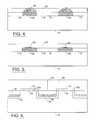
- FIG. 5is a cross section of a substrate on which a layer of GaN has been *epitaxially grown in accordance with an aspect of the present invention.
- FIG. 6is a cross section of a substrate on which a layer of GaN has been epitaxially grown in accordance with another aspect of the present invention.
- FIG. 6Ais a cross section of a substrate on which a pair of raised portions has been formed and a mask layer has been deposited.
- FIG. 6Bis a cross section of a substrate on which a pair of raised portions has been formed and a mask layer has been deposited using a self-alignment technique.
- FIG. 7is a cross-sectional SEM image showing the interruption of lateral growth of a GaN layer by crystals nucleating on the mask.
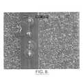
- FIG. 8is a plan view SEM image of two GaN stripes in which crystallites on the underlying mask disturbed the epitaxial growth.
- FIG. 9is a cross-sectional SEM of GaN stripes grown in accordance with an embodiment of the present invention using a reflective mask layer.
- FIG. 10is a cross-sectional SEM of GaN stripes grown in accordance with an embodiment of the present invention until adjacent regions have coalesced over the reflective masks.
- FIG. 11is a cross-sectional SEM of a GaN layer grown on a conductive buffer layer over a Si 3 N 4 mask.
- FIG. 12is a cross sectional SEM of a GaN layer grown in accordance with a second embodiment of the present invention.
- FIG. 13is a plan view SEM image of two GaN stripes grown in accordance with the second embodiment of the present invention.
- FIG. 14is a cross-sectional TEM (Transmission Electron Microscopy) image of a firs layer of GaN grown in accordance with the present invention.
- FIG. 15is a cross-sectional SEM of GaN stripes grown in accordance with an embodiment of the present invention while maintaining a ratio of lateral to horizontal growth rates of 4.2:1.
- FIG. 16is a cross-sectional SEM of GaN stripes grown in accordance with an embodiment of the present invention while maintaining a ratio of lateral to horizontal growth rates of 1:1.
- Stripes 14 a , 14 bare characterized in that they have a width (w) and are separated by mask openings or windows 6 having a window length (l).
- the mask layermay be deposited using plasma enhanced chemical vapor deposition (PECVD), sputtering, electron-beam deposition, thermal oxidation or other deposition techniques, and patterned using standard photolithographic techniques.
- PECVDplasma enhanced chemical vapor deposition
- sputteringsputtering
- electron-beam depositionelectron-beam deposition
- thermal oxidationthermal oxidation or other deposition techniques
- Photolithographic techniquesare well known in the art.
- the mask layer 14may comprise silicon nitride (Si x N y ) or silicon dioxide (SiO 2 ) or any other suitable mask material. If the structure being fabricated is intended for use in an optical device such as an LED or laser diode, the mask layer 14 may comprise a reflective or refractory metal which is stable in ammonia and hydrogen gas, has a melting point in excess of about 1200° C., and is reflective to the desired wavelength. Examples of such metals include tungsten (W) and platinum (Pt). Alternatively, the mask layer could comprise a Bragg reflector which may comprise alternating layers of Si x N y and SiO 2 or other oxides, the design of which is well known in the art.
- the substratemay be silicon carbide, sapphire (Al 2 O 3 ), silicon, ZnO, or any other similarly suitable substrate.
- Silicon carbide substratesare advantageous for a number of reasons. Silicon carbide provides closer lattice and thermal expansion matches for GaN, is thermally and chemically stable, has natural cleave planes, high thermal conductivity, and is transparent to visible wavelengths up to 380 nm. Also, silicon carbide has a distinct advantage in that it is conductive, which permits fabrication of vertical-geometry devices. Silicon carbide substrates may have a polytype of 4H, 6H, 3C or 15R. Preferably, however, the substrate is 6H—SiC (on-axis).
- substrate 10is well known to those in the art. Fabrication of silicon carbide substrates are described, for example, in U.S. Pat. Nos. 4,865,685 to Palmour et al., Re34,861 to Davis, et al., U.S. Pat. No. 4,912,064 to Kong et al., and U.S. Pat. No. 4,946,547 to Palmour et al., the disclosures of each of which are hereby incorporated by reference. The fabrication of sapphire and silicon substrates is well known in the art and need not be described in detail.
- an epitaxial layer 20may be fabricated by first growing a buffer layer 12 on the surface of the substrate 10 .
- Epitaxial layer 20may comprise gallium nitride or a Group III-nitride alloy thereof, such as aluminum gallium nitride (AlGaN), indium gallium nitride (InGaN), or aluminum indium gallium nitride (AlInGaN).
- the buffer layerpreferably comprises a layer 12 of Al x Ga 1-x N, where x represents the mole fraction of aluminum present in the alloy and 0 ⁇ 1.
- the buffer layer 12may have the structure described in copending and commonly assigned U.S. patent application Ser. No. 08/944,547 entitled “Group III Nitride Photonic Devices on Silicon Carbide Substrates with Conductive Buffer Interlayer Structure,” filed Oct. 7, 1997, the disclosure of which is hereby incorporated herein by reference.
- the topmost buffer layercomprises a mole percentage of Al of between 9% and 12%, and is approximately 1000 to 5000 ⁇ thick.
- the buffer layer 12may be made conductive to the SiC substrate by the formation of capped GaN dots on the SiC substrate as described in U.S. patent application Ser. No. 08/944,547 prior to the deposition of the buffer layer.
- a low temperature GaN, AlN or AlGaN buffermay be grown.
- an AlGaN buffer layer 12may be grown vertically from the mask openings 6 using a vapor phase epitaxy (VPE) technique such as hydride vapor phase epitaxy (HVPE), or more preferably metal-organic vapor phase epitaxy (MOVPE).
- VPEvapor phase epitaxy
- HVPEhydride vapor phase epitaxy
- MOVPEmetal-organic vapor phase epitaxy
- the buffer layer 12is grown to a thickness larger than the thickness of the mask layer 14 .
- the epitaxial layer 20is then grown by VPE, preferably in the same run or step as the buffer layer was grown.
- epitaxial layer 20grows laterally (i.e. parallel to the face of the substrate) in addition to vertically. Lateral growth fronts 22 move across the surface of the mask stripes 14 as layer 20 grows.
- epitaxial layer 20grows laterally until the growth fronts 22 coalesce at interfaces 24 to form a continuous layer 20 of gallium nitride.
- a useful portion of layer 20may be fabricated without coalescence of adjacent portions.
- a laser diode stripemay be fabricated in a region of layer 20 that has not coalesced.
- a coalesced layeris preferred.
- an LED device 250 ⁇ wide and 275 ⁇ longmay be fabricated on a coalesced layer of gallium nitride grown in accordance with the present invention.
- the buffer layer 12 and the overgrown layer 20may be grown using trimethylgallium (TMG), trimethylaluminum (TMA) and ammonia (NH 3 ) precursors in a diluent of H 2 .
- TMGtrimethylgallium
- TMAtrimethylaluminum
- NH 3ammonia
- a suitable MOVPE growth techniqueis described in greater detail in T. Weeks et al., “ GaN thin films deposited via organometallic vapor phase epitaxy on ⁇ (6 H )— SiC (0001) using high - tenmperature monocrystalline AlN buffer layers, ” Appl. Phys. Let., Vol. 67, No. 3, Jul. 1995, pp. 401-403.
- nucleation and growth of polycrystalline Al x Ga 1-x N 30typically begins to occur on the exposed upper surfaces of mask stripes 14 .
- the lateral growth of layer 20will be interrupted, preventing it from forming a desired width of laterally overgrown material, and/or preventing it from coalescing with adjacent regions.
- the polycrystalline Al x Ga 1-x N 30 on the maskgrows vertically and blocks the lateral growth of the single crystal layer 20 .
- the present inventorshave discovered that it is possible, by controlling the horizontal and vertical growth rates of layer 20 , to avoid interruption of the laterally growing layer 20 by the polycrystalline Al x Ga 1-x N 30.
- nucleation on the maskneed not be controlled, since layer 20 will overgrow any polycrystalline nucleation and growth on the mask.
- the mechanisms for controlling the relevant growth factorswill now be described in detail.
- the lateral and vertical growth rates of the overgrown layer 20are controlled by a number of factors.
- One controlling factoris the so called “fill factor”, defined herein as the ratio of the window length (l) to the stripe period (p).
- a higher fill factori.e. a larger window length for a given period
- a lower fill factorresults in an increased vertical growth rate.
- Other factors for controlling the lateral and vertical growth ratesare growth temperature, source gas flow rates, source gas nitrogen/gallium ratio, and growth pressure.
- the growth conditionscan be adjusted to increase the vertical growth rate.
- a lateral growth rate of about 2-8 ⁇ /hr and a vertical growth rate of about 1-2 ⁇ /hrshould be selected.
- a lateral growth rate of 6.3 ⁇ /hr and a vertical growth rate of 1.5 ⁇ /hr (4.2:1 ratio)may be achieved by growing the layer 20 by MOVPE at 1110° C. and 200 Torr on a patterned mask of Si x N y stripes having a stripe width of 10 ⁇ , a window width of 25 ⁇ and a period of 35 ⁇ for a fill factor of 0.71.
- the N/Ga ratio during growth of the layer 20is preferably about 2500. Ratios of lateral growth rate to vertical growth rate may exceed 4.2:1.
- TMGmay flowed at 34.8 ⁇ mol/min
- TMAmay be flowed at 6.5 ⁇ mol/min
- ammoniamay be flowed at a rate of 10 slpm in a diluent of H 2 at 15.5 slpm.
- the layer 20may be grown by flowing TMG at 309 ⁇ mol/min and ammonia at a rate of 17 slpm in a diluent of H 2 at 22.5 slpm until the GaN layer has grown to a desired thickness.
- a lateral and vertical growth rate of 4.2 ⁇ /hr (1:1 ratio)may be achieved by growing the layer 20 by MOVPE at 1060° C. and 200 Torr on a patterned mask of Si x N y stripes having a stripe width of 10 ⁇ , a window length of 25 ⁇ and a period of 35 ⁇ for a fill factor of 0.71.
- the N/Ga ratio during growth of the layer 20is preferably about 2500. It will be appreciated that other ratios, including ratios greater than 4.2:1, may be achieved through selection of other growth parameters.
- FIG. 6An embodiment of the present invention utilizing pendeoepitaxial growth is illustrated in FIG. 6 .
- the substrate 10is etched to form at least one raised portion 15 , which defines adjacent recessed areas or trenches 18 on the substrate 10 .
- FIG. 6illustrates an embodiment in which a pair of raised portions 15 a , 15 b have been patterned using standard photolithographic techniques and reactive ion etching.
- the height of raised portions 15i.e. the depth of trenches 18
- a mask layer 14which may be Si x N y , SiO 2 or any other suitable mask is then deposited on the upper surface of substrate 10 , with mask openings 16 made on the upper surfaces of raised portions 15 a , 15 b.
- the substrate 10may be silicon carbide, sapphire, silicon, gallium arsenide, gallium nitride or another Group III-nitride such as aluminum nitride or aluminum gallium nitride.
- the fabrication of aluminum nitride substratesis described in U.S. Pat. Nos. 5,858,086 and 5,954,874 to Hunter, the disclosures of which are hereby incorporated herein by reference.
- Gallium nitride substrateshave been fabricated by growing thick epitaxial layers of gallium nitride on a non-GaN substrate. Other methods of obtaining gallium nitride substrates are summarized in A.
- an AlGaN buffer layer 12may be grown vertically from the mask openings (or windows) 16 using MOVPE.
- the buffer layer 12is grown to a thickness larger than the thickness of the mask layer 14 .
- the pendeoepitaxial layer 26is then grown. Pendeoepitaxial layer 26 grows laterally (i.e. parallel to the face of the substrate) over trenches 18 in addition to vertically.
- nucleation and growth of polycrystalline GaN 30may be occurring on the mask 14 , it is occurring within trenches 18 , and thus does not interfere with the lateral growth of pendeoepitaxial layer 26 .
- FIG. 12is a cross sectional SEM of a pendeoepitaxial GaN layer grown in accordance with this embodiment of the invention. Polycrystalline AlGaN material is evident within the trench, but does not interfere with the lateral growth of the GaN layer.
- Trenches 18may be fabricated with depths less than or greater than 1 ⁇ if desired or necessary depending on the rate of polycrystalline growth on the mask or the width of the pendeoepitaxial layer to be grown.
- pendeoepitaxial layer 26grows laterally until opposing growth fronts 22 coalesce at interfaces 24 to form a continuous layer 26 of gallium nitride.
- FIG. 13is a plan view SEM image of two pendeoepitaxial GaN stripes grown in accordance with this embodiment of the present invention.
- FIGS. 6A and 6Balternative methods of forming the mask layer 14 are illustrated in FIGS. 6A and 6B.
- raised portions 15may be formed using standard etching techniques. Typically, this involves patterning the surface of a substrate with an etch mask, etching the substrate to the desired depth, and then removing the etch mask. As shown in FIG. 6A, after the etch mask has been removed, the mask layer 14 may be formed on the surface of substrate 10 by PECVD. Windows 16 are then opened in mask 14 to reveal the upper surfaces of raised portions 15 .
- FIG. 6 BA simplified method of forming mask 14 is illustrated in FIG. 6 B.
- an etch mask 19is applied to the surface of substrate 10 , and substrate 10 is etched to form trenches 18 .
- Mask 14is deposited after etching trenches 18 but prior to removing etch mask 19 .
- mask 14preferably comprises a thin mask layer of about 50-200 ⁇ in thickness.
- Mask 14may comprise Si x N y , SiO 2 , or any other suitable mask material.
- Etch mask 19is then removed, revealing the upper surfaces of raised portions 15 .
- the edges of windows 16 in mask 14are thereby self-aligned with the edges of raised portions 15 .
- only a single masking stepis required and it is not necessary to use photolithographic techniques to open windows 16 in mask layer 14 .
- FIG. 7is a cross-sectional SEM image showing the interruption of lateral growth of a GaN layer by crystals nucleating on the mask.
- FIG. 8is a plan view SEM image of two GaN stripes in which crystallites on the underlying mask disturbed the epitaxial growth.
- FIG. 9is a cross-sectional SEM of GaN stripes grown in accordance with an embodiment of the present invention using a reflector mask layer.
- FIG. 10is a cross-sectional SEM of GaN stripes grown in accordance with an embodiment of the present invention until adjacent regions have coalesced over the masks.
- FIG. 11is a cross-sectional SEM of a GaN layer grown on a conductive buffer layer over a Si 3 N 4 mask.
- FIG. 14is a cross-sectional TEM (Transmission Electron Microscopy) image of a layer of GaN grown in accordance with the present invention.
- the defect densities observedindicate an estimated reduction from approximately 10 9 /cm 2 in the regions over the windows to approximately 10 6 /cm 2 in the regions above the mask stripes.
- a patterned mask of Si x N y stripes having a stripe width of 10 ⁇ , a window length of 25 ⁇ and a period of 35 ⁇ for a fill factor of 0.715was applied to a 6H—SiC substrate.
- the stripeswere arranged parallel to the ⁇ 1100 > direction.
- a 0.5 ⁇ thick Al 0.1 Ga 0.9 N buffer layerwas grown by MOVPE by flowing TMG at 34.8 ⁇ mol/min, TMA at 6.5 ⁇ mol/min and ammonia at 10 slpm in a diluent of H 2 at 15.5 slpm at 1020° C. and 76 Torr for a total of 80 minutes.
- FIG. 15is an SEM image a cross section of the resulting GaN layer.
- a patterned mask of Si x N y stripes having a stripe width of 10 ⁇ , a window length of 25 ⁇ and a period of 35 ⁇ for a fill factor of 0.715was applied to a 6H—SiC substrate.
- the stripeswere arranged parallel to the ⁇ 1100 > direction.
- a 0.5 ⁇ thick Al 0.1 Ga 0.9 N buffer layerwas grown by MOVPE by flowing TMG at 34.8 ⁇ mol/min, TMA at 6.51 ⁇ mol/min and ammonia at 10 slpm in a diluent of H 2 at 15.5 slpm at 1050° C. and 76 Torr for a total of 80 minutes.
- FIG. 16is an SEM image a cross section of the resulting GaN layer.
Landscapes
- Engineering & Computer Science (AREA)
- Physics & Mathematics (AREA)
- Condensed Matter Physics & Semiconductors (AREA)
- General Physics & Mathematics (AREA)
- Manufacturing & Machinery (AREA)
- Computer Hardware Design (AREA)
- Microelectronics & Electronic Packaging (AREA)
- Power Engineering (AREA)
- Chemical & Material Sciences (AREA)
- Materials Engineering (AREA)
- Led Devices (AREA)
Abstract
Description
This is a continuation of Ser. No. 09/679,799, filed Oct. 5, 2000 which claims benefit of S. No. 60/159,299 filed Oct. 14, 1999.
The present invention relates to electronic device structures and fabrication methods, and more particularly to Group III-nitride semiconductor structures and methods of fabrication by pendeo- and lateral epitaxial overgrowth.
Gallium nitride (GaN) is a wide-bandgap semiconductor material widely known for its usefulness as an active layer in blue light emitting diodes. GaN is also under investigation for use in other microelectronic devices including laser diodes and high-speed, high power transistor devices. As used herein, “gallium nitride” or “GaN” refers to gallium nitride and III-nitride alloys thereof, including aluminum gallium nitride (AlGaN), indium gallium nitride (InGaN) and aluminum indium gallium nitride (AlInGaN).
High-quality bulk crystals of GaN are currently unavailable for commercial use. Thus, GaN crystals are typically fabricated as heteroepitaxial layers on underlying non-GaN substrates. Unfortunately, GaN has a considerable lattice mismatch with most suitable substrate crystals. For example, GaN has a 15% lattice mismatch with sapphire and a 3.5% lattice mismatch with silicon carbide. Lattice mismatches between a substrate and an epitaxial layer cause threading dislocations which may propagate through the growing epitaxial layer. Even when grown on silicon carbide with an aluminum nitride buffer layer, a GaN epitaxial layer exhibits dislocation densities estimated to be in excess of 108/cm2. Such defect densities limit the usefulness of GaN in highly sensitive electronic devices such as laser diodes.
Lateral Epitaxial Overgrowth (LEO) of GaN has been the subject of considerable interest since it was first introduced as a method of reducing the dislocation densities of epitaxially grown GaN films. Essentially, the technique consists of masking an underlying layer of GaN with a mask having a pattern of openings and growing the GaN up through and laterally onto the mask. It was found that the portion of the GaN layer grown laterally over the mask exhibits a much lower dislocation density than the underlying GaN layer or the portion of the GaN layer above the mask openings. As used herein, “lateral” or “horizontal” refers to a direction generally parallel to the surface of a substrate, while the term “vertical” means a direction generally orthogonal to the surface of a substrate.
One drawback to conventional LEO techniques is that separate process steps are required for growing the underlying GaN layer, masking the GaN layer and then growing the lateral layer. Early embodiments of LEO did not place the mask directly on the non-GaN substrate because unwanted nucleation would occur on the mask during nucleation of the GaN layer at low temperatures, preventing adjacent laterally-grown regions from coalescing (or otherwise from growing laterally a desired distance if coalescence is not required). When the mask is placed directly on a GaN layer, unwanted nucleation on the mask is typically not a problem since low temperature nucleation is not required and the growth temperature of GaN is very high, typically above 1000° C. During high temperature growth, unwanted nucleation does not occur on the mask due to the much higher sticking coefficient of gallium atoms on the gallium nitride surface as compared to the mask.
This drawback is addressed with some success by a “single step” process for LEO. Shealy et al. disclosed a process whereby an underlying SiC or sapphire substrate was masked with silicon nitride. The process is referred to as “single step” because it does not require growth of an intermediate layer of GaN between the substrate and the mask. Shealy found that minimizing nucleation on the silicon nitride mask permitted growth of a relatively defect free layer of laterally-grown GaN over the masks. However, under certain circumstances it is desirable to avoid having to minimize nucleation on the mask, yet still be able to grow a relatively defect free layer of GaN in a single step process.
Accordingly, there is a need in the art for a method of fabricating a relatively defect-free single crystal film of gallium nitride in a single step process without having to minimize nucleation on the mask layer.
Moreover, there is a need in the art for a method of fabricating a relatively defect-free single crystal film of gallium nitride in a single step process without having to minimize nucleation on the mask layer which provides a conductive buffer layer to permit electrical communication between a conductive substrate and an epitaxial layer of gallium nitride.
It is an object of the present invention to provide a method of fabricating a relatively defect-free single crystal film of gallium nitride in a single step process without having to minimize nucleation on the mask layer.
It is a further object of the present invention to provide a method of fabricating a relatively defect-free single crystal film of gallium nitride in a single step process without having to minimize nucleation on the mask layer which provides a conductive buffer layer to permit electrical communication between a conductive substrate and an epitaxial layer of gallium nitride
The foregoing and other objects are achieved by a method of fabricating a gallium g0 nitride-based semiconductor structure on a substrate. The method includes the steps of forming a mask having at least one opening therein directly on the substrate, growing a buffer layer through said at least one opening, and growing a layer of gallium nitride upwardly from said buffer layer and laterally across said mask. During growth of the gallium nitride from the mask, the vertical and horizontal growth rates of the gallium nitride layer are maintained at rates sufficient to prevent polycrystalline material nucleating on said mask from interrupting the lateral growth of the gallium nitride layer.
In an alternative embodiment, the method includes forming at least one raised portion defining adjacent trenches in the substrate and forming a mask on the substrate, the mask having at least one opening over the upper surface of the raised portion. A buffer layer may be grown from the upper surface of the raised portion. The gallium nitride layer is then grown laterally by pendeoepitaxy over the trenches.
In another embodiment, the present invention provides a gallium nitride-based semiconductor structure on a substrate. The structure includes a substrate and a mask having at least one window therein applied directly on the upper surface of the substrate. An overgrown layer of gallium nitride extends upwardly from the mask window and laterally across the mask, on which polycrystalline material has nucleated and grown.
In another embodiment, the substrate includes at least one raised portion defining adjacent trenches. A mask structure overlays the substrate and a window in the mask exposes at least a portion of the upper surface of the raised portion. An overgrown layer of gallium nitride extends upwardly from the mask window and laterally over the trench and across the mask, on which polycrystalline material has nucleated and grown.
FIG. 1 is a cross-section of a substrate on which a mask has been patterned.
FIG. 2 is a plan view of a substrate on which a mask has been patterned.
FIG. 3 is a cross section of a substrate on which a layer of GaN has been epitaxially grown by LEO on a conductive buffer layer.
FIG. 3A is a cross section of a substrate on which a layer of GaN is being epitaxially grown by LEO on a conductive buffer layer, but has not coalesced.
FIG. 4 is a cross section of a substrate on which excessive nucleation on the mask has interrupted the lateral growth of a layer, of GaN.
FIG. 5 is a cross section of a substrate on which a layer of GaN has been *epitaxially grown in accordance with an aspect of the present invention.
FIG. 6 is a cross section of a substrate on which a layer of GaN has been epitaxially grown in accordance with another aspect of the present invention.
FIG. 6A is a cross section of a substrate on which a pair of raised portions has been formed and a mask layer has been deposited.
FIG. 6B is a cross section of a substrate on which a pair of raised portions has been formed and a mask layer has been deposited using a self-alignment technique.
FIG. 7 is a cross-sectional SEM image showing the interruption of lateral growth of a GaN layer by crystals nucleating on the mask.
FIG. 8 is a plan view SEM image of two GaN stripes in which crystallites on the underlying mask disturbed the epitaxial growth.
FIG. 9 is a cross-sectional SEM of GaN stripes grown in accordance with an embodiment of the present invention using a reflective mask layer.
FIG. 10 is a cross-sectional SEM of GaN stripes grown in accordance with an embodiment of the present invention until adjacent regions have coalesced over the reflective masks.
FIG. 11 is a cross-sectional SEM of a GaN layer grown on a conductive buffer layer over a Si3N4mask.
FIG. 12 is a cross sectional SEM of a GaN layer grown in accordance with a second embodiment of the present invention.
FIG. 13 is a plan view SEM image of two GaN stripes grown in accordance with the second embodiment of the present invention.
FIG. 14 is a cross-sectional TEM (Transmission Electron Microscopy) image of a firs layer of GaN grown in accordance with the present invention.
FIG. 15 is a cross-sectional SEM of GaN stripes grown in accordance with an embodiment of the present invention while maintaining a ratio of lateral to horizontal growth rates of 4.2:1.
FIG. 16 is a cross-sectional SEM of GaN stripes grown in accordance with an embodiment of the present invention while maintaining a ratio of lateral to horizontal growth rates of 1:1.
The present invention will now be described more fully hereinafter with reference to the accompanying drawings, in which preferred embodiments of the invention are shown. This invention may, however, be embodied in many different forms and should not be construed as limited to the embodiments set forth herein. Rather, these embodiments are provided so that this disclosure will be thorough and complete, and will fully convey the scope of the invention to those skilled in the art. Like numbers refer to like elements throughout. Furthermore, the various layers and regions illustrated in the figures are illustrated schematically. As will also be appreciated by those of skill in the art, references herein to a layer formed “on” a substrate or other layer may refer to the layer formed directly on the substrate or other layer or on an intervening layer or layers formed on the substrate or other layer. References herein to a layer formed “directly on” a substrate or other layer refer to the layer formed on the substrate without an intervening layer or layers formed on the substrate or other layer. The present invention is not limited to the relative size and spacing illustrated in the accompanying figures.
Basic LEO techniques are described in A. Usui, et al., “Thick GaN epitaxial growth with low dislocation density by hydride vapor phase epitaxy,” Jpn. J. Appl. Phys. Vol. 36, pp. L899-902 (1997). Various LEO techniques including pendeoepitaxial techniques are described in U.S. application Ser. No. 09/032,190 “Gallium Nitride Semiconductor Structures Including a Lateral Gallium Nitride Layer that Extends Prom an Underlying Gallium Nitride Layer”, filed Feb. 27, 1998; application Ser. No. 09/031,843 “Gallium Nitride Semiconductor Structures Including Laterally Offset Patterned Layers”, filed Feb. 27, 1998; application Ser. No. 09/198,784, “Pendeoepitaxial Methods of Fabricating Gallium Nitride Semiconductor Layers on Silicon Carbide Substrates by Lateral Growth from Sidewalls of Masked Posts, and Gallium Nitride Semiconductor Structures Fabricated Thereby” filed Nov. 24, 1998; and application Serial No. 60/088,761 “Methods of Fabricating Gallium Nitride Semiconductor Layers by Lateral Growth from Sidewalls into Trenches, and Gallium Nitride Semiconductor Structures Fabricated Thereby,” filed Jun. 10, 1998, the disclosures of each of which are hereby incorporated herein by reference.
Referring now to FIG. 1, asubstrate 10 is illustrated on which is deposited amask layer 14 comprisingstripes stripes Stripes windows 6 having a window length (l). The distance between an edge ofstripe 14aand the corresponding edge ofstripe 14bis defined as the period (p) of the mask pattern, at least with respect tostripes
The mask layer may be deposited using plasma enhanced chemical vapor deposition (PECVD), sputtering, electron-beam deposition, thermal oxidation or other deposition techniques, and patterned using standard photolithographic techniques. The PECVD process is described in detail inChapter 6 of S. M. Sze,VLSI Technology,2nd ed., McGraw-Hill 1988. Photolithographic techniques are well known in the art.
As illustrated in FIG. 2,stripes mask layer 14 may comprise silicon nitride (SixNy) or silicon dioxide (SiO2) or any other suitable mask material. If the structure being fabricated is intended for use in an optical device such as an LED or laser diode, themask layer 14 may comprise a reflective or refractory metal which is stable in ammonia and hydrogen gas, has a melting point in excess of about 1200° C., and is reflective to the desired wavelength. Examples of such metals include tungsten (W) and platinum (Pt). Alternatively, the mask layer could comprise a Bragg reflector which may comprise alternating layers of SixNyand SiO2or other oxides, the design of which is well known in the art.
The substrate may be silicon carbide, sapphire (Al2O3), silicon, ZnO, or any other similarly suitable substrate. Silicon carbide substrates are advantageous for a number of reasons. Silicon carbide provides closer lattice and thermal expansion matches for GaN, is thermally and chemically stable, has natural cleave planes, high thermal conductivity, and is transparent to visible wavelengths up to 380 nm. Also, silicon carbide has a distinct advantage in that it is conductive, which permits fabrication of vertical-geometry devices. Silicon carbide substrates may have a polytype of 4H, 6H, 3C or 15R. Preferably, however, the substrate is 6H—SiC (on-axis).
The fabrication ofsubstrate 10 is well known to those in the art. Fabrication of silicon carbide substrates are described, for example, in U.S. Pat. Nos. 4,865,685 to Palmour et al., Re34,861 to Davis, et al., U.S. Pat. No. 4,912,064 to Kong et al., and U.S. Pat. No. 4,946,547 to Palmour et al., the disclosures of each of which are hereby incorporated by reference. The fabrication of sapphire and silicon substrates is well known in the art and need not be described in detail.
Referring now to FIG. 3, anepitaxial layer 20 may be fabricated by first growing abuffer layer 12 on the surface of thesubstrate 10.Epitaxial layer 20 may comprise gallium nitride or a Group III-nitride alloy thereof, such as aluminum gallium nitride (AlGaN), indium gallium nitride (InGaN), or aluminum indium gallium nitride (AlInGaN). For a SiC substrate, the buffer layer preferably comprises alayer 12 of AlxGa1-xN, where x represents the mole fraction of aluminum present in the alloy and 0<×≦1. In the case of silicon carbide substrates, thebuffer layer 12 may have the structure described in copending and commonly assigned U.S. patent application Ser. No. 08/944,547 entitled “Group III Nitride Photonic Devices on Silicon Carbide Substrates with Conductive Buffer Interlayer Structure,” filed Oct. 7, 1997, the disclosure of which is hereby incorporated herein by reference.
Preferably, the topmost buffer layer comprises a mole percentage of Al of between 9% and 12%, and is approximately 1000 to 5000 Å thick. Thebuffer layer 12 may be made conductive to the SiC substrate by the formation of capped GaN dots on the SiC substrate as described in U.S. patent application Ser. No. 08/944,547 prior to the deposition of the buffer layer.
For sapphire or silicon substrates, a low temperature GaN, AlN or AlGaN buffer may be grown.
As shown in FIG. 3, anAlGaN buffer layer 12 may be grown vertically from themask openings 6 using a vapor phase epitaxy (VPE) technique such as hydride vapor phase epitaxy (HVPE), or more preferably metal-organic vapor phase epitaxy (MOVPE). In a preferred embodiment, thebuffer layer 12 is grown to a thickness larger than the thickness of themask layer 14. Once thebuffer layer 12 has been grown to a desired thickness, theepitaxial layer 20 is then grown by VPE, preferably in the same run or step as the buffer layer was grown.
As shown in FIG. 3A,epitaxial layer 20 grows laterally (i.e. parallel to the face of the substrate) in addition to vertically.Lateral growth fronts 22 move across the surface of themask stripes 14 aslayer 20 grows.
Referring again to FIG. 3, in one embodiment,epitaxial layer 20 grows laterally until thegrowth fronts 22 coalesce atinterfaces 24 to form acontinuous layer 20 of gallium nitride. However, it is not necessary for the growth fronts to coalesce for all applications, as it is possible to fabricate devices in laterally overgrown portions of GaN even if they have not coalesced with adjacent portions. As illustrated in FIG. 9, a useful portion oflayer 20 may be fabricated without coalescence of adjacent portions. For example, a laser diode stripe may be fabricated in a region oflayer 20 that has not coalesced. For fabrication of an LED, a coalesced layer is preferred. For example, an LED device 250 μ wide and 275 μ long may be fabricated on a coalesced layer of gallium nitride grown in accordance with the present invention.
Thebuffer layer 12 and theovergrown layer 20 may be grown using trimethylgallium (TMG), trimethylaluminum (TMA) and ammonia (NH3) precursors in a diluent of H2. A suitable MOVPE growth technique is described in greater detail in T. Weeks et al., “GaN thin films deposited via organometallic vapor phase epitaxy on α(6H)—SiC(0001)using high-tenmperature monocrystalline AlN buffer layers,” Appl. Phys. Let., Vol. 67, No. 3, Jul. 1995, pp. 401-403.
While thelayer 20 of gallium nitride is growing, nucleation and growth of polycrystalline AlxGa1-xN 30 typically begins to occur on the exposed upper surfaces ofmask stripes 14. As illustrated in FIG. 4, if the growth rate of AlxGa1-xN on the masks is too high, the lateral growth oflayer 20 will be interrupted, preventing it from forming a desired width of laterally overgrown material, and/or preventing it from coalescing with adjacent regions. Essentially, the polycrystalline AlxGa1-xN 30 on the mask grows vertically and blocks the lateral growth of thesingle crystal layer 20.
The present inventors have discovered that it is possible, by controlling the horizontal and vertical growth rates oflayer 20, to avoid interruption of the laterally growinglayer 20 by the polycrystalline AlxGa1-xN 30. By increasing the lateral growth rate oflayer 20 relative to its vertical growth rate by a given amount depending on the geometry of the structure, it is possible to grow alayer 20 that will grow to a desired distance despite nucleation on the mask.
Stated differently, by maintaining a sufficiently high lateral growth rate relative to the vertical growth rate oflayer 20, nucleation on the mask need not be controlled, sincelayer 20 will overgrow any polycrystalline nucleation and growth on the mask.
As a particular example, it has been discovered that by maintaining a ratio of lateral growth rate to vertical growth rate of at least 1:1, it is possible to grow a laterally-overgrown GaN layer on a stripe having a width of 5 μ in a pattern with a period of 30 μ from a nucleation layer having an Al concentration of about 10%. By maintaining a lateral/vertical growth ratio of 4:1, it is possible to grow a layer of GaN over a mask having 25 μ-wide stripes. As shown in FIG. 5, when the lateral growth rate is caused to exceed the vertical growth rate by a sufficient amount, the growth fronts of thelayer 20 may coalesce before the polycrystalline AlGaN growing on thestripes 14a,bgrow large enough to block them.
The mechanisms for controlling the relevant growth factors will now be described in detail. The lateral and vertical growth rates of theovergrown layer 20 are controlled by a number of factors. One controlling factor is the so called “fill factor”, defined herein as the ratio of the window length (l) to the stripe period (p). For a given window length, a higher fill factor (i.e. a larger window length for a given period) results in a slower vertical growth rate. Conversely, for a given window length, a lower fill factor results in an increased vertical growth rate. Other factors for controlling the lateral and vertical growth rates are growth temperature, source gas flow rates, source gas nitrogen/gallium ratio, and growth pressure.
If desired, once the laterally growinggrowth fronts 22 of thelayer 20 have coalesced over the masks, the growth conditions can be adjusted to increase the vertical growth rate.
Although dependent on the structure of the particular epitaxial growth reactor being employed, typical growth parameters for the rates described herein are summarized in the following table.
| TABLE 1 |
| Typical growth parameters. |
| Parameter | Value | ||
| Growth temperature | 1060-1120° C. | ||
| Growth pressure | 50-200 Torr | ||
| N/Ga ratio | 2500 | ||
| Fill factor | 0.714-0.833 | ||
| Lateral growth rate/vertical growth rate | 1-4.2 | ||
Preferably, a lateral growth rate of about 2-8 μ/hr and a vertical growth rate of about 1-2 μ/hr should be selected. A lateral growth rate of 6.3 μ/hr and a vertical growth rate of 1.5 μ/hr (4.2:1 ratio) may be achieved by growing thelayer 20 by MOVPE at 1110° C. and 200 Torr on a patterned mask of SixNystripes having a stripe width of 10μ, a window width of 25μ and a period of 35μ for a fill factor of 0.71. The N/Ga ratio during growth of thelayer 20 is preferably about 2500. Ratios of lateral growth rate to vertical growth rate may exceed 4.2:1.
To grow the buffer layer, TMG may flowed at 34.8 μmol/min, TMA may be flowed at 6.5 μmol/min and ammonia may be flowed at a rate of 10 slpm in a diluent of H2at 15.5 slpm. Once the buffer layer has been grown to a desired thickness, thelayer 20 may be grown by flowing TMG at 309 μmol/min and ammonia at a rate of 17 slpm in a diluent of H2at 22.5 slpm until the GaN layer has grown to a desired thickness.
A lateral and vertical growth rate of 4.2 μ/hr (1:1 ratio) may be achieved by growing thelayer 20 by MOVPE at 1060° C. and 200 Torr on a patterned mask of SixNystripes having a stripe width of 10 μ, a window length of 25 μ and a period of 35 μ for a fill factor of 0.71. The N/Ga ratio during growth of thelayer 20 is preferably about 2500. It will be appreciated that other ratios, including ratios greater than 4.2:1, may be achieved through selection of other growth parameters.
An embodiment of the present invention utilizing pendeoepitaxial growth is illustrated in FIG.6. In this embodiment, thesubstrate 10 is etched to form at least one raisedportion 15, which defines adjacent recessed areas ortrenches 18 on thesubstrate 10. FIG. 6 illustrates an embodiment in which a pair of raisedportions mask layer 14, which may be SixNy, SiO2or any other suitable mask is then deposited on the upper surface ofsubstrate 10, withmask openings 16 made on the upper surfaces of raisedportions
In this embodiment, thesubstrate 10 may be silicon carbide, sapphire, silicon, gallium arsenide, gallium nitride or another Group III-nitride such as aluminum nitride or aluminum gallium nitride. The fabrication of aluminum nitride substrates is described in U.S. Pat. Nos. 5,858,086 and 5,954,874 to Hunter, the disclosures of which are hereby incorporated herein by reference. Gallium nitride substrates have been fabricated by growing thick epitaxial layers of gallium nitride on a non-GaN substrate. Other methods of obtaining gallium nitride substrates are summarized in A. Usui, et al., “Thick GaN epitaxial growth with low dislocation density by hydride vapor phase epitaxy,” Jpn. J. Appl. Phys. Vol. 36, pp. L899-902 (1997). It will be appreciated by those of skill in the art that when the substrate is a Group III-nitride, homoepitaxial growth may be used.
As shown in FIG. 6, if a buffer layer is required, anAlGaN buffer layer 12 may be grown vertically from the mask openings (or windows)16 using MOVPE. In a preferred embodiment, thebuffer layer 12 is grown to a thickness larger than the thickness of themask layer 14. Once thebuffer layer 12 has been grown to a desired thickness, thependeoepitaxial layer 26 is then grown.Pendeoepitaxial layer 26 grows laterally (i.e. parallel to the face of the substrate) overtrenches 18 in addition to vertically.
Although nucleation and growth ofpolycrystalline GaN 30 may be occurring on themask 14, it is occurring withintrenches 18, and thus does not interfere with the lateral growth ofpendeoepitaxial layer 26.
FIG. 12 is a cross sectional SEM of a pendeoepitaxial GaN layer grown in accordance with this embodiment of the invention. Polycrystalline AlGaN material is evident within the trench, but does not interfere with the lateral growth of the GaN layer.
It will be readily appreciated that a trench depth of 1μ is exemplary.Trenches 18 may be fabricated with depths less than or greater than 1μ if desired or necessary depending on the rate of polycrystalline growth on the mask or the width of the pendeoepitaxial layer to be grown.
In one embodiment,pendeoepitaxial layer 26 grows laterally until opposinggrowth fronts 22 coalesce atinterfaces 24 to form acontinuous layer 26 of gallium nitride. However, as mentioned above, it is not necessary for thegrowth fronts 22 to coalesce for all applications, as it is possible to fabricate devices in laterally overgrown portions of GaN even if they have not coalesced with adjacent portions.
FIG. 13 is a plan view SEM image of two pendeoepitaxial GaN stripes grown in accordance with this embodiment of the present invention.
For the embodiment illustrated in FIG. 6, alternative methods of forming themask layer 14 are illustrated in FIGS. 6A and 6B. As discussed above, raisedportions 15 may be formed using standard etching techniques. Typically, this involves patterning the surface of a substrate with an etch mask, etching the substrate to the desired depth, and then removing the etch mask. As shown in FIG. 6A, after the etch mask has been removed, themask layer 14 may be formed on the surface ofsubstrate 10 by PECVD.Windows 16 are then opened inmask 14 to reveal the upper surfaces of raisedportions 15.
Because of the tolerance limitations of photolithographic techniques, when thewindows 16 are opened inmask 14, it is difficult to align the edges ofwindows 16 with the edges of raisedportions 15. Thus, there is someoverlap 17 of themask 14 onto the upper surfaces of raisedportions 15.
A simplified method of formingmask 14 is illustrated in FIG.6B. In this method, anetch mask 19 is applied to the surface ofsubstrate 10, andsubstrate 10 is etched to formtrenches 18.Mask 14 is deposited after etchingtrenches 18 but prior to removingetch mask 19. In this technique,mask 14 preferably comprises a thin mask layer of about 50-200 Å in thickness.Mask 14 may comprise SixNy, SiO2, or any other suitable mask material.Etch mask 19 is then removed, revealing the upper surfaces of raisedportions 15. The edges ofwindows 16 inmask 14 are thereby self-aligned with the edges of raisedportions 15. Thus, with this technique, only a single masking step is required and it is not necessary to use photolithographic techniques to openwindows 16 inmask layer 14.
FIG. 7 is a cross-sectional SEM image showing the interruption of lateral growth of a GaN layer by crystals nucleating on the mask.
FIG. 8 is a plan view SEM image of two GaN stripes in which crystallites on the underlying mask disturbed the epitaxial growth.
FIG. 9 is a cross-sectional SEM of GaN stripes grown in accordance with an embodiment of the present invention using a reflector mask layer.
FIG. 10 is a cross-sectional SEM of GaN stripes grown in accordance with an embodiment of the present invention until adjacent regions have coalesced over the masks.
FIG. 11 is a cross-sectional SEM of a GaN layer grown on a conductive buffer layer over a Si3N4mask.
FIG. 14 is a cross-sectional TEM (Transmission Electron Microscopy) image of a layer of GaN grown in accordance with the present invention. The defect densities observed indicate an estimated reduction from approximately 109/cm2in the regions over the windows to approximately 106/cm2in the regions above the mask stripes.
A patterned mask of SixNystripes having a stripe width of 10μ, a window length of 25μ and a period of 35μ for a fill factor of 0.715 was applied to a 6H—SiC substrate. The stripes were arranged parallel to the <1100> direction. A 0.5μ thick Al0.1Ga0.9N buffer layer was grown by MOVPE by flowing TMG at 34.8 μmol/min, TMA at 6.5 μmol/min and ammonia at 10 slpm in a diluent of H2at 15.5 slpm at 1020° C. and 76 Torr for a total of 80 minutes. Following growth of the buffer layer, an epitaxial layer of GaN was grown by MOVPE by flowing TMG at 309 μmol/min and ammonia at 17 slpm in a diluent of H2at 22.5 slpm at 1110° C. and 200 Torr for 45 minutes. The ratio of lateral to vertical growth under these conditions was approximately 4.2:1. FIG. 15 is an SEM image a cross section of the resulting GaN layer.
A patterned mask of SixNystripes having a stripe width of 10μ, a window length of 25μ and a period of 35μ for a fill factor of 0.715 was applied to a 6H—SiC substrate. The stripes were arranged parallel to the <1100> direction. A 0.5μ thick Al0.1Ga0.9N buffer layer was grown by MOVPE by flowing TMG at 34.8 μmol/min, TMA at 6.51 μmol/min and ammonia at 10 slpm in a diluent of H2at 15.5 slpm at 1050° C. and 76 Torr for a total of 80 minutes. Following growth of the buffer layer, an epitaxial layer of GaN was grown by MOVPE by flowing TMG at 309 μmol/min and ammonia at 17 slpm in a diluent of H2at 22.5 slpm at 1060° C. and 200 Torr for one hour. The ratio of lateral to vertical growth under these conditions was approximately 1:1. FIG. 16 is an SEM image a cross section of the resulting GaN layer.
In the specification and drawings, there have been set forth preferred and exemplary embodiments of the invention which have been included by way of example and not by way of limitation, the scope of the invention being set forth in the accompanying claims.
Claims (15)
1. A method of fabricating a gallium nitride-based semiconductor structure on a substrate, the method comprising:
forming a mask on a substrate that includes both at least one trench and at least one raised portion adjacent said trench, and with said mask having at least one opening therein on said raised portion of said substrate;
growing a buffer layer on said raised portion of said substrate within said opening in said mask; and
growing an epitaxial layer selected from the group consisting of gallium nitride and Group III nitride alloys of gallium nitride upwardly from said buffer layer and laterally across said trench.
2. A fabrication method according toclaim 1 comprising growing the buffer layer to a thickness greater than the thickness of the mask.
3. A fabrication method according toclaim 1 comprising forming at least two raised portions adjacent to the trench and growing the epitaxial layer until it coalesces over the trench.
4. A fabrication method according toclaim 1 wherein the step of forming the mask comprises forming the mask and then forming the opening therein.
5. A fabrication method according toclaim 1 comprising forming the mask on a silicon carbide substrate.
6. A method of fabricating a gallium nitride-based semiconductor structure on a substrate, the method comprising:
forming at least one trench in a substrate to thereby define both the trench and a raised portion immediately adjacent the trench;
forming a mask on the trenched substrate with the mask having at least one opening therein on the raised portion of the substrate;
growing a buffer layer on the raised portion of the substrate through the opening in the mask; and
growing an epitaxial layer selected from the group consisting of gallium nitride and Group III nitride alloys of gallium nitride upwardly from the buffer layer and laterally across the trench.
7. A fabrication method according toclaim 6 wherein the step of forming the trench comprising etching the trench in the substrate.
8. A fabrication method according toclaim 7 wherein the etching step comprises a reactive ion etch.
9. A fabrication method according toclaim 6 wherein the step of forming the buffer comprises forming the buffer using vapor phase epitaxy.
10. A fabrication method according toclaim 6 comprising growing the buffer layer to a thickness greater than the thickness of the mask.
11. A fabrication method according toclaim 6 comprising forming at least two raised portions adjacent to the trench and growing the epitaxial layer until it coalesces over the trench portion.
12. A fabrication method according toclaim 6 wherein the step of forming the mask comprises forming the mask and then forming the opening therein.
13. A fabrication method according toclaim 6 comprising forming the mask using a technique selected from the group consisting of plasma-enhanced chemical vapor deposition, sputtering, reactive sputtering, electron-beam deposition and thermal oxidation.
14. A method of fabricating a gallium nitride-based semiconductor structure on a substrate, the method comprising:
forming a mask on a substrate that includes bath at least one trench and at least two raised portions adjacent said trench, and with said mask having at least one opening therein on said raised portion of said substrate;
growing a buffer layer on said raised portion of said substrate within said opening in said mask; and
growing an epitaxial layer selected from the group consisting of gallium nitride and Group III nitride alloys of gallium nitride upwardly from said buffer layer and laterally across said trench until it coalesces over said trench.
15. A method of fabricating a gallium nitride-based semiconductor structure on a substrate, the method comprising:
forming at least one trench in a substrate to thereby define both the trench and at least two raised portions immediately adjacent the trench;
forming a mask on the trenched substrate with the mask having at least one opening therein on the raised portion of the substrate;
growing a buffer layer on the raised portion of the substrate through the opening in the mask; and
growing an epitaxial layer selected from the group consisting of gallium nitride and Group III nitride alloys of gallium nitride upwardly from the buffet layer and laterally across the trench until it coalesces over the trench.
Priority Applications (1)
| Application Number | Priority Date | Filing Date | Title |
|---|---|---|---|
| US09/934,270US6582986B2 (en) | 1999-10-14 | 2001-08-21 | Single step pendeo-and lateral epitaxial overgrowth of group III-nitride epitaxial layers with group III-nitride buffer layer and resulting structures |
Applications Claiming Priority (3)
| Application Number | Priority Date | Filing Date | Title |
|---|---|---|---|
| US15929999P | 1999-10-14 | 1999-10-14 | |
| US09/679,799US6812053B1 (en) | 1999-10-14 | 2000-10-05 | Single step pendeo- and lateral epitaxial overgrowth of Group III-nitride epitaxial layers with Group III-nitride buffer layer and resulting structures |
| US09/934,270US6582986B2 (en) | 1999-10-14 | 2001-08-21 | Single step pendeo-and lateral epitaxial overgrowth of group III-nitride epitaxial layers with group III-nitride buffer layer and resulting structures |
Related Parent Applications (1)
| Application Number | Title | Priority Date | Filing Date |
|---|---|---|---|
| US09/679,799ContinuationUS6812053B1 (en) | 1999-10-14 | 2000-10-05 | Single step pendeo- and lateral epitaxial overgrowth of Group III-nitride epitaxial layers with Group III-nitride buffer layer and resulting structures |
Publications (2)
| Publication Number | Publication Date |
|---|---|
| US20020022290A1 US20020022290A1 (en) | 2002-02-21 |
| US6582986B2true US6582986B2 (en) | 2003-06-24 |
Family
ID=26855818
Family Applications (5)
| Application Number | Title | Priority Date | Filing Date |
|---|---|---|---|
| US09/679,799Expired - LifetimeUS6812053B1 (en) | 1999-10-14 | 2000-10-05 | Single step pendeo- and lateral epitaxial overgrowth of Group III-nitride epitaxial layers with Group III-nitride buffer layer and resulting structures |
| US09/934,270Expired - LifetimeUS6582986B2 (en) | 1999-10-14 | 2001-08-21 | Single step pendeo-and lateral epitaxial overgrowth of group III-nitride epitaxial layers with group III-nitride buffer layer and resulting structures |
| US10/056,607Expired - LifetimeUS6764932B2 (en) | 1999-10-14 | 2002-01-24 | Single step pendeo- and lateral epitaxial overgrowth of group III-nitride epitaxial layers with group III-nitride buffer layer and resulting structures |
| US10/427,984Expired - LifetimeUS6803602B2 (en) | 1999-10-14 | 2003-05-02 | Single step pendeo- and lateral epitaxial overgrowth of Group III-nitride epitaxial layers with Group III-nitride buffer layer and resulting structures |
| US10/685,597Expired - LifetimeUS6955977B2 (en) | 1999-10-14 | 2003-10-16 | Single step pendeo-and lateral epitaxial overgrowth of group III-nitride epitaxial layers with group III-nitride buffer layer and resulting structures |
Family Applications Before (1)
| Application Number | Title | Priority Date | Filing Date |
|---|---|---|---|
| US09/679,799Expired - LifetimeUS6812053B1 (en) | 1999-10-14 | 2000-10-05 | Single step pendeo- and lateral epitaxial overgrowth of Group III-nitride epitaxial layers with Group III-nitride buffer layer and resulting structures |
Family Applications After (3)
| Application Number | Title | Priority Date | Filing Date |
|---|---|---|---|
| US10/056,607Expired - LifetimeUS6764932B2 (en) | 1999-10-14 | 2002-01-24 | Single step pendeo- and lateral epitaxial overgrowth of group III-nitride epitaxial layers with group III-nitride buffer layer and resulting structures |
| US10/427,984Expired - LifetimeUS6803602B2 (en) | 1999-10-14 | 2003-05-02 | Single step pendeo- and lateral epitaxial overgrowth of Group III-nitride epitaxial layers with Group III-nitride buffer layer and resulting structures |
| US10/685,597Expired - LifetimeUS6955977B2 (en) | 1999-10-14 | 2003-10-16 | Single step pendeo-and lateral epitaxial overgrowth of group III-nitride epitaxial layers with group III-nitride buffer layer and resulting structures |
Country Status (1)
| Country | Link |
|---|---|
| US (5) | US6812053B1 (en) |
Cited By (64)
| Publication number | Priority date | Publication date | Assignee | Title |
|---|---|---|---|---|
| US20030092263A1 (en)* | 1999-12-24 | 2003-05-15 | Masayoshi Koike | Method for producing group III nitride compound semiconductor and group III nitride compound semiconductor device |
| US20030119239A1 (en)* | 2000-03-31 | 2003-06-26 | Masayoshi Koike | Production method of III nitride compound semiconductor and III nitride compound semiconductor element |
| US20030139037A1 (en)* | 2001-03-27 | 2003-07-24 | Toshimasa Kobayashi | Nitrde semiconductor element and production method thereof |
| US20030145783A1 (en)* | 2001-10-09 | 2003-08-07 | Sumitomo Electric Industries, Ltd. | Single crystal GaN substrate, method of growing single crystal GaN and method of producing single crystal GaN substrate |
| US20030198837A1 (en)* | 2002-04-15 | 2003-10-23 | Craven Michael D. | Non-polar a-plane gallium nitride thin films grown by metalorganic chemical vapor deposition |
| US20030227026A1 (en)* | 2002-02-27 | 2003-12-11 | Osamu Goto | Nitride semiconductor, semiconductor device, and manufacturing methods for the same |
| US20040087055A1 (en)* | 2001-05-09 | 2004-05-06 | Nsc-Nanosemiconductor Gmbh | Semiconductor device and method of making same |
| WO2004061909A1 (en)* | 2002-12-16 | 2004-07-22 | The Regents Of The University Of California | Growth of reduced dislocation density non-polar gallium nitride by hydride vapor phase epitaxy |
| US20040159851A1 (en)* | 2003-02-13 | 2004-08-19 | Edmond John Adam | Group III nitride contact structures for light emitting devices |
| US20040159843A1 (en)* | 2003-02-14 | 2004-08-19 | Edmond John Adam | Inverted light emitting diode on conductive substrate |
| US20040159842A1 (en)* | 2003-02-13 | 2004-08-19 | Edmond John Adam | Group III nitride LED with silicon carbide cladding layer |
| US20040206299A1 (en)* | 1999-03-17 | 2004-10-21 | Mitsubishi Cable Industries, Ltd. | Semiconductor base and its manufacturing method, and semiconductor crystal manufacturing method |
| US20050029533A1 (en)* | 2003-05-09 | 2005-02-10 | Yifeng Wu | LED fabrication via ion implant isolation |
| US20050142876A1 (en)* | 2003-10-24 | 2005-06-30 | Katona Thomas M. | Maskless lateral epitaxial overgrowth of aluminum nitride and high aluminum composition aluminum gallium nitride |
| US20050184302A1 (en)* | 2000-04-04 | 2005-08-25 | Toshimasa Kobayashi | Nitride semiconductor device and method of manufacturing the same |
| US20050194584A1 (en)* | 2003-11-12 | 2005-09-08 | Slater David B.Jr. | LED fabrication via ion implant isolation |
| US20050214992A1 (en)* | 2002-12-16 | 2005-09-29 | The Regents Of The University Of California | Fabrication of nonpolar indium gallium nitride thin films, heterostructures and devices by metalorganic chemical vapor deposition |
| US20050245095A1 (en)* | 2002-04-15 | 2005-11-03 | The Regents Of The University Of California | Growth of planar reduced dislocation density m-plane gallium nitride by hydride vapor phase epitaxy |
| US20050258450A1 (en)* | 2004-05-20 | 2005-11-24 | Saxler Adam W | Semiconductor devices having a hybrid channel layer, current aperture transistors and methods of fabricating same |
| US20050263065A1 (en)* | 2004-05-26 | 2005-12-01 | Negley Gerald H | Vapor assisted growth of gallium nitride |
| US20050285126A1 (en)* | 2004-05-06 | 2005-12-29 | Yifeng Wu | LED fabrication via ion implant isolation |
| US20060008941A1 (en)* | 2002-12-16 | 2006-01-12 | Basf Aktiengesellschaft | Growth of planar, non-polar a-plane gallium nitride by hydride vapor phase epitaxy |
| US20060017064A1 (en)* | 2004-07-26 | 2006-01-26 | Saxler Adam W | Nitride-based transistors having laterally grown active region and methods of fabricating same |
| US20060108606A1 (en)* | 2004-11-23 | 2006-05-25 | Saxler Adam W | Cap layers and/or passivation layers for nitride-based transistors, transistor structures and methods of fabricating same |
| US20060118823A1 (en)* | 2004-12-06 | 2006-06-08 | Primit Parikh | Field effect transistors (FETs) having multi-watt output power at millimeter-wave frequencies |
| US20060118809A1 (en)* | 2004-12-06 | 2006-06-08 | Primit Parikh | High power density and/or linearity transistors |
| US7101444B2 (en) | 2001-05-09 | 2006-09-05 | Nl Nanosemiconductor Gmbh | Defect-free semiconductor templates for epitaxial growth |
| US20060208280A1 (en)* | 2005-03-15 | 2006-09-21 | Smith Richard P | Group III nitride field effect transistors (FETS) capable of withstanding high temperature reverse bias test conditions |
| US20060226413A1 (en)* | 2005-04-11 | 2006-10-12 | Saxler Adam W | Composite substrates of conductive and insulating or semi-insulating group III-nitrides for group III-nitride devices |
| US20060226412A1 (en)* | 2005-04-11 | 2006-10-12 | Saxler Adam W | Thick semi-insulating or insulating epitaxial gallium nitride layers and devices incorporating same |
| US20060244011A1 (en)* | 2005-04-29 | 2006-11-02 | Saxler Adam W | Binary group III-nitride based high electron mobility transistors and methods of fabricating same |
| US20060244010A1 (en)* | 2005-04-29 | 2006-11-02 | Saxler Adam W | Aluminum free group III-nitride based high electron mobility transistors and methods of fabricating same |
| US20060267043A1 (en)* | 2005-05-27 | 2006-11-30 | Emerson David T | Deep ultraviolet light emitting devices and methods of fabricating deep ultraviolet light emitting devices |
| US20060270076A1 (en)* | 2005-05-31 | 2006-11-30 | The Regents Of The University Of California | Defect reduction of non-polar and semi-polar III-nitrides with sidewall lateral epitaxial overgrowth (SLEO) |
| US20060276043A1 (en)* | 2003-03-21 | 2006-12-07 | Johnson Mark A L | Method and systems for single- or multi-period edge definition lithography |
| US20070004184A1 (en)* | 2005-06-29 | 2007-01-04 | Saxler Adam W | Low dislocation density group III nitride layers on silicon carbide substrates and methods of making the same |
| US20070018198A1 (en)* | 2005-07-20 | 2007-01-25 | Brandes George R | High electron mobility electronic device structures comprising native substrates and methods for making the same |
| US20070111488A1 (en)* | 2004-05-10 | 2007-05-17 | The Regents Of The University Of California | Fabrication of nonpolar indium gallium nitride thin films, heterostructures and devices by metalorganic chemical vapor deposition |
| US20070164322A1 (en)* | 2006-01-17 | 2007-07-19 | Cree, Inc. | Methods of fabricating transistors including dielectrically-supported gate electrodes and related devices |
| US20070164315A1 (en)* | 2004-11-23 | 2007-07-19 | Cree, Inc. | Cap Layers Including Aluminum Nitride for Nitride-Based Transistors and Methods of Fabricating Same |
| US20070184637A1 (en)* | 2004-06-03 | 2007-08-09 | The Regents Of The University Of California | Growth of planar reduced dislocation density m-plane gallium nitride by hydride vapor phase epitaxy |
| US20070197004A1 (en)* | 2006-02-23 | 2007-08-23 | Armin Dadgar | Nitride semiconductor component and process for its production |
| US20080113496A1 (en)* | 2006-11-15 | 2008-05-15 | The Regents Of The University Of California | METHOD FOR HETEROEPITAXIAL GROWTH OF HIGH-QUALITY N-FACE GaN, InN, AND AlN AND THEIR ALLOYS BY METAL ORGANIC CHEMICAL VAPOR DEPOSITION |
| US20080135853A1 (en)* | 2002-04-15 | 2008-06-12 | The Regents Of The University Of California | Dislocation reduction in non-polar iii-nitride thin films |
| US20080149936A1 (en)* | 2006-11-17 | 2008-06-26 | Stmicroelectronics Sa | Process for integratng a iii-n type component on a (001) nominal silicium substrate |
| US20080163814A1 (en)* | 2006-12-12 | 2008-07-10 | The Regents Of The University Of California | CRYSTAL GROWTH OF M-PLANE AND SEMIPOLAR PLANES OF (Al, In, Ga, B)N ON VARIOUS SUBSTRATES |
| US20080272462A1 (en)* | 2004-11-22 | 2008-11-06 | Toshitaka Shimamoto | Nitride-Based Semiconductor Device and Method for Fabricating the Same |
| US20090152565A1 (en)* | 2007-12-14 | 2009-06-18 | Brandes George R | Pendeo epitaxial structures and devices |
| US20090166650A1 (en)* | 2007-12-28 | 2009-07-02 | Advanced Optoelectronic Technology Inc. | Light-emitting device of group iii nitride-based semiconductor and manufacturing method thereof |
| US20090224289A1 (en)* | 2006-01-17 | 2009-09-10 | Cree, Inc. | Transistors including supported gate electrodes |
| US20090246944A1 (en)* | 2006-11-15 | 2009-10-01 | The Regents Of The University Of California | METHOD FOR HETEROEPITAXIAL GROWTH OF HIGH-QUALITY N-FACE GaN, InN, AND AlN AND THEIR ALLOYS BY METAL ORGANIC CHEMICAL VAPOR DEPOSITION |
| US20100011109A1 (en)* | 2003-11-17 | 2010-01-14 | Pierre Lescuyer | Method for Safety Control of Data Exchange Flows Between a Communications Module and a Communications Network and Said Communications Module |
| US20100074826A1 (en)* | 2006-12-08 | 2010-03-25 | Eric Aujol | Method for manufacturing a single crystal of nitride by epitaxial growth on a substrate preventing growth on the edges of the substrate |
| US20100090312A1 (en)* | 2006-08-31 | 2010-04-15 | Industrial Technology Research Institute | Nitride semiconductor structure and method for manufacturing the same |
| US20120043578A1 (en)* | 2010-08-23 | 2012-02-23 | Su-Hui Lin | GaN-Based Light-Emitting Diode and Method for Manufacturing the Same |
| US20120112320A1 (en)* | 2009-06-01 | 2012-05-10 | Mitsubishi Chemical Corporation | Nitride semiconductor crystal and production process thereof |
| US8674393B2 (en) | 2010-12-21 | 2014-03-18 | Industrial Technology Research Institute | Substrate structure and fabrication thereof, and light emitting diode devices fabricated from the same |
| US20150102358A1 (en)* | 2013-10-11 | 2015-04-16 | Panasonic Intellectual Property Management Co., Ltd. | Nitride semiconductor multilayer structure, semiconductor light-emitting device, and method for manufacturing nitride semiconductor multilayer structure |
| US20160013275A1 (en)* | 2012-11-30 | 2016-01-14 | Soft-Epi Inc. | Iii-nitride semiconductor stacked structure |
| US20170352535A1 (en)* | 2014-11-20 | 2017-12-07 | Osram Opto Semiconductors Gmbh | Method of producing an optoelectronic semiconductor chip and optoelectronic semiconductor chip |
| US10923348B2 (en) | 2019-05-29 | 2021-02-16 | International Business Machines Corporation | Gate-all-around field effect transistor using template-assisted-slective-epitaxy |
| US10937860B2 (en) | 2019-03-14 | 2021-03-02 | International Business Machines Corporation | Nanosheet transistor bottom isolation |
| US20230078017A1 (en)* | 2021-09-16 | 2023-03-16 | Wolfspeed, Inc. | Semiconductor device incorporating a substrate recess |
| US20240355918A1 (en)* | 2023-04-21 | 2024-10-24 | Woflspeed, Inc. | Heteroepitaxial semiconductor devices with enhanced thermal dissipation |
Families Citing this family (93)
| Publication number | Priority date | Publication date | Assignee | Title |
|---|---|---|---|---|
| JP3007971B1 (en)* | 1999-03-01 | 2000-02-14 | 東京大学長 | Method of forming single crystal thin film |
| JP3702700B2 (en)* | 1999-03-31 | 2005-10-05 | 豊田合成株式会社 | Group III nitride compound semiconductor device and method for manufacturing the same |
| JP3438674B2 (en)* | 1999-10-21 | 2003-08-18 | 松下電器産業株式会社 | Method for manufacturing nitride semiconductor device |
| EP1104031B1 (en)* | 1999-11-15 | 2012-04-11 | Panasonic Corporation | Nitride semiconductor laser diode and method of fabricating the same |
| US6403451B1 (en)* | 2000-02-09 | 2002-06-11 | Noerh Carolina State University | Methods of fabricating gallium nitride semiconductor layers on substrates including non-gallium nitride posts |
| US7619261B2 (en)* | 2000-08-07 | 2009-11-17 | Toyoda Gosei Co., Ltd. | Method for manufacturing gallium nitride compound semiconductor |
| US6956250B2 (en)* | 2001-02-23 | 2005-10-18 | Nitronex Corporation | Gallium nitride materials including thermally conductive regions |
| JP3956637B2 (en)* | 2001-04-12 | 2007-08-08 | ソニー株式会社 | Nitride semiconductor crystal growth method and semiconductor element formation method |
| US6939730B2 (en)* | 2001-04-24 | 2005-09-06 | Sony Corporation | Nitride semiconductor, semiconductor device, and method of manufacturing the same |
| DE10203801A1 (en)* | 2002-01-31 | 2003-08-21 | Osram Opto Semiconductors Gmbh | Semiconductor component and method for its production |
| US7399684B2 (en)* | 2002-07-11 | 2008-07-15 | University College Cork - National University Of Ireland, Cork | Defect reduction in semiconductor materials |
| US6900067B2 (en)* | 2002-12-11 | 2005-05-31 | Lumileds Lighting U.S., Llc | Growth of III-nitride films on mismatched substrates without conventional low temperature nucleation layers |
| DE60311678T2 (en)* | 2002-12-20 | 2007-11-22 | Cree, Inc. | METHOD FOR PRODUCING SEMICONDUCTOR DEVICES WITH MESASTRUCTURES AND MULTIPLE PASSIVATION LAYERS AND RELATED DEVICES |
| KR100512580B1 (en)* | 2003-12-31 | 2005-09-06 | 엘지전자 주식회사 | Method of growing nitride semiconductor thin film having small defects |
| US7198970B2 (en)* | 2004-01-23 | 2007-04-03 | The United States Of America As Represented By The Secretary Of The Navy | Technique for perfecting the active regions of wide bandgap semiconductor nitride devices |
| US7872268B2 (en)* | 2004-04-22 | 2011-01-18 | Cree, Inc. | Substrate buffer structure for group III nitride devices |
| US7977694B2 (en)* | 2006-11-15 | 2011-07-12 | The Regents Of The University Of California | High light extraction efficiency light emitting diode (LED) with emitters within structured materials |
| US7259402B2 (en)* | 2004-09-22 | 2007-08-21 | Cree, Inc. | High efficiency group III nitride-silicon carbide light emitting diode |
| US8174037B2 (en)* | 2004-09-22 | 2012-05-08 | Cree, Inc. | High efficiency group III nitride LED with lenticular surface |
| US8513686B2 (en)* | 2004-09-22 | 2013-08-20 | Cree, Inc. | High output small area group III nitride LEDs |
| US7737459B2 (en)* | 2004-09-22 | 2010-06-15 | Cree, Inc. | High output group III nitride light emitting diodes |
| WO2006062084A1 (en)* | 2004-12-08 | 2006-06-15 | Sumitomo Electric Industries, Ltd. | Semiconductor laser device and method for manufacturing same |
| US8288942B2 (en)* | 2004-12-28 | 2012-10-16 | Cree, Inc. | High efficacy white LED |
| US20060270201A1 (en)* | 2005-05-13 | 2006-11-30 | Chua Soo J | Nano-air-bridged lateral overgrowth of GaN semiconductor layer |
| US9153645B2 (en) | 2005-05-17 | 2015-10-06 | Taiwan Semiconductor Manufacturing Company, Ltd. | Lattice-mismatched semiconductor structures with reduced dislocation defect densities and related methods for device fabrication |
| EP2595175B1 (en)* | 2005-05-17 | 2019-04-17 | Taiwan Semiconductor Manufacturing Company, Ltd. | Method of fabricating a lattice-mismatched semiconductor structure with reduced dislocation defect densities |
| US8324660B2 (en) | 2005-05-17 | 2012-12-04 | Taiwan Semiconductor Manufacturing Company, Ltd. | Lattice-mismatched semiconductor structures with reduced dislocation defect densities and related methods for device fabrication |
| KR100638869B1 (en)* | 2005-06-21 | 2006-10-27 | 삼성전기주식회사 | A method of forming a nitride compound layer and a method of manufacturing a BAN substrate and a vertical structure nitride semiconductor light emitting device using the same |
| KR101329388B1 (en) | 2005-07-26 | 2013-11-14 | 앰버웨이브 시스템즈 코포레이션 | Solutions for integrated circuit integration of alternative active area materials |
| US7638842B2 (en) | 2005-09-07 | 2009-12-29 | Amberwave Systems Corporation | Lattice-mismatched semiconductor structures on insulators |
| US20070054467A1 (en)* | 2005-09-07 | 2007-03-08 | Amberwave Systems Corporation | Methods for integrating lattice-mismatched semiconductor structure on insulators |
| JP2009519202A (en)* | 2005-12-12 | 2009-05-14 | キーマ テクノロジーズ, インク. | Group III nitride product and method for producing the same |
| US7772604B2 (en) | 2006-01-05 | 2010-08-10 | Illumitex | Separate optical device for directing light from an LED |
| WO2007112066A2 (en) | 2006-03-24 | 2007-10-04 | Amberwave Systems Corporation | Lattice-mismatched semiconductor structures and related methods for device fabrication |
| KR101038069B1 (en) | 2006-04-25 | 2011-06-01 | 내셔널 유니버시티 오브 싱가포르 | Method of zinc oxide film grown on epitaxial lateral overgrowth gallium nitride template |
| US7560364B2 (en)* | 2006-05-05 | 2009-07-14 | Applied Materials, Inc. | Dislocation-specific lateral epitaxial overgrowth to reduce dislocation density of nitride films |
| US7459380B2 (en)* | 2006-05-05 | 2008-12-02 | Applied Materials, Inc. | Dislocation-specific dielectric mask deposition and lateral epitaxial overgrowth to reduce dislocation density of nitride films |
| WO2007142946A2 (en) | 2006-05-31 | 2007-12-13 | Cree Led Lighting Solutions, Inc. | Lighting device and method of lighting |
| JP5155536B2 (en)* | 2006-07-28 | 2013-03-06 | 一般財団法人電力中央研究所 | Method for improving the quality of SiC crystal and method for manufacturing SiC semiconductor device |
| US8173551B2 (en) | 2006-09-07 | 2012-05-08 | Taiwan Semiconductor Manufacturing Co., Ltd. | Defect reduction using aspect ratio trapping |
| WO2008039495A1 (en) | 2006-09-27 | 2008-04-03 | Amberwave Systems Corporation | Tri-gate field-effect transistors formed by aspect ratio trapping |
| WO2008039534A2 (en) | 2006-09-27 | 2008-04-03 | Amberwave Systems Corporation | Quantum tunneling devices and circuits with lattice- mismatched semiconductor structures |
| WO2008042351A2 (en) | 2006-10-02 | 2008-04-10 | Illumitex, Inc. | Led system and method |
| US20080083431A1 (en)* | 2006-10-06 | 2008-04-10 | Mark Schwarze | Device and method for clearing debris from the front of a hood in a mechanized sweepers |
| US8502263B2 (en) | 2006-10-19 | 2013-08-06 | Taiwan Semiconductor Manufacturing Company, Ltd. | Light-emitter-based devices with lattice-mismatched semiconductor structures |
| WO2008057454A2 (en)* | 2006-11-02 | 2008-05-15 | The Regents Of The University Of California | Growth and manufacture of reduced dislocation density and free-standing aluminum nitride films by hydride vapor phase epitaxy |
| US8304805B2 (en) | 2009-01-09 | 2012-11-06 | Taiwan Semiconductor Manufacturing Company, Ltd. | Semiconductor diodes fabricated by aspect ratio trapping with coalesced films |
| WO2008124154A2 (en) | 2007-04-09 | 2008-10-16 | Amberwave Systems Corporation | Photovoltaics on silicon |
| US8237151B2 (en) | 2009-01-09 | 2012-08-07 | Taiwan Semiconductor Manufacturing Company, Ltd. | Diode-based devices and methods for making the same |
| US7825328B2 (en) | 2007-04-09 | 2010-11-02 | Taiwan Semiconductor Manufacturing Company, Ltd. | Nitride-based multi-junction solar cell modules and methods for making the same |
| US8329541B2 (en) | 2007-06-15 | 2012-12-11 | Taiwan Semiconductor Manufacturing Company, Ltd. | InP-based transistor fabrication |
| EP2171748A1 (en)* | 2007-07-26 | 2010-04-07 | S.O.I.Tec Silicon on Insulator Technologies | Epitaxial methods and templates grown by the methods |
| JP2009049044A (en)* | 2007-08-13 | 2009-03-05 | Sumitomo Electric Ind Ltd | Method for fabricating a semiconductor laser |
| JP2010538495A (en) | 2007-09-07 | 2010-12-09 | アンバーウェーブ・システムズ・コーポレーション | Multi-junction solar cell |
| JP2011512037A (en) | 2008-02-08 | 2011-04-14 | イルミテックス, インコーポレイテッド | System and method for emitter layer shaping |
| US8183667B2 (en) | 2008-06-03 | 2012-05-22 | Taiwan Semiconductor Manufacturing Co., Ltd. | Epitaxial growth of crystalline material |
| US8274097B2 (en) | 2008-07-01 | 2012-09-25 | Taiwan Semiconductor Manufacturing Company, Ltd. | Reduction of edge effects from aspect ratio trapping |
| US8981427B2 (en) | 2008-07-15 | 2015-03-17 | Taiwan Semiconductor Manufacturing Company, Ltd. | Polishing of small composite semiconductor materials |
| US8377796B2 (en) | 2008-08-11 | 2013-02-19 | Taiwan Semiconductor Manufacturing Company, Ltd. | III-V compound semiconductor epitaxy from a non-III-V substrate |
| US8803189B2 (en)* | 2008-08-11 | 2014-08-12 | Taiwan Semiconductor Manufacturing Company, Ltd. | III-V compound semiconductor epitaxy using lateral overgrowth |
| EP2335273A4 (en)* | 2008-09-19 | 2012-01-25 | Taiwan Semiconductor Mfg | FORMATION OF DEVICES BY GROWTH OF EPITAXIAL LAYERS |
| US20100072515A1 (en) | 2008-09-19 | 2010-03-25 | Amberwave Systems Corporation | Fabrication and structures of crystalline material |
| US8253211B2 (en) | 2008-09-24 | 2012-08-28 | Taiwan Semiconductor Manufacturing Company, Ltd. | Semiconductor sensor structures with reduced dislocation defect densities |
| TW201034256A (en) | 2008-12-11 | 2010-09-16 | Illumitex Inc | Systems and methods for packaging light-emitting diode devices |
| CN102257600A (en)* | 2008-12-16 | 2011-11-23 | 惠普开发有限公司 | Semiconductor structure having an elog on a thermally and electrically conductive mask |
| US8629446B2 (en) | 2009-04-02 | 2014-01-14 | Taiwan Semiconductor Manufacturing Company, Ltd. | Devices formed from a non-polar plane of a crystalline material and method of making the same |
| US8449128B2 (en) | 2009-08-20 | 2013-05-28 | Illumitex, Inc. | System and method for a lens and phosphor layer |
| US8585253B2 (en) | 2009-08-20 | 2013-11-19 | Illumitex, Inc. | System and method for color mixing lens array |
| SG169921A1 (en)* | 2009-09-18 | 2011-04-29 | Taiwan Semiconductor Mfg | Improved fabrication and structures of crystalline material |
| SG169922A1 (en)* | 2009-09-24 | 2011-04-29 | Taiwan Semiconductor Mfg | Improved semiconductor sensor structures with reduced dislocation defect densities and related methods for the same |
| US8450190B2 (en)* | 2010-03-23 | 2013-05-28 | Academia Sinica | Fabrication of GaN substrate by defect selective passivation |
| WO2011132285A1 (en)* | 2010-04-22 | 2011-10-27 | 三菱電機株式会社 | Semiconductor device and method for manufacturing same |
| TWI562195B (en) | 2010-04-27 | 2016-12-11 | Pilegrowth Tech S R L | Dislocation and stress management by mask-less processes using substrate patterning and methods for device fabrication |
| CN102237454A (en)* | 2010-04-29 | 2011-11-09 | 展晶科技(深圳)有限公司 | Semiconductor photoelectric element and manufacturing method thereof |
| JP2012033708A (en)* | 2010-07-30 | 2012-02-16 | Sumitomo Electric Ind Ltd | Manufacturing method of semiconductor device |
| JP2012089612A (en)* | 2010-10-18 | 2012-05-10 | Sumitomo Electric Ind Ltd | Composite substrate having silicon carbide substrate |
| JP2012119429A (en)* | 2010-11-30 | 2012-06-21 | Sanken Electric Co Ltd | Method of manufacturing semiconductor device, and semiconductor device |
| KR101810609B1 (en)* | 2011-02-14 | 2017-12-20 | 삼성전자주식회사 | Semiconductor device and method of manufacturing the same |
| JP2015521365A (en)* | 2012-04-13 | 2015-07-27 | タンデム スン アーベー | Manufacturing method of semiconductor method device based on epitaxial growth |
| CN103378237B (en)* | 2012-04-25 | 2016-04-13 | 清华大学 | epitaxial structure |
| US9142400B1 (en) | 2012-07-17 | 2015-09-22 | Stc.Unm | Method of making a heteroepitaxial layer on a seed area |
| JP2014049616A (en)* | 2012-08-31 | 2014-03-17 | Sony Corp | Diode and manufacturing method of diode |
| US20150059640A1 (en)* | 2013-08-27 | 2015-03-05 | Raytheon Company | Method for reducing growth of non-uniformities and autodoping during column iii-v growth into dielectric windows |
| US9640422B2 (en)* | 2014-01-23 | 2017-05-02 | Intel Corporation | III-N devices in Si trenches |
| US9490119B2 (en) | 2014-05-21 | 2016-11-08 | Palo Alto Research Center Incorporated | Fabrication of thin-film devices using selective area epitaxy |
| WO2016056960A1 (en)* | 2014-10-07 | 2016-04-14 | Tandem Sun Ab | Method for manufacturing a semiconductor device and semiconductor device |
| US9773906B2 (en) | 2015-04-28 | 2017-09-26 | Samsung Electronics Co., Ltd. | Relaxed semiconductor layers with reduced defects and methods of forming the same |
| CN106952976A (en)* | 2016-01-06 | 2017-07-14 | 上海桐钰电力科技有限公司 | A kind of ultraviolet photodetector and preparation method thereof |
| DE102016105063A1 (en) | 2016-03-18 | 2017-09-21 | Osram Opto Semiconductors Gmbh | Diffractive optical element, method of making a diffractive optical element and laser device |
| US9960127B2 (en) | 2016-05-18 | 2018-05-01 | Macom Technology Solutions Holdings, Inc. | High-power amplifier package |
| US10134658B2 (en) | 2016-08-10 | 2018-11-20 | Macom Technology Solutions Holdings, Inc. | High power transistors |
| JP7073767B2 (en)* | 2018-02-09 | 2022-05-24 | 富士電機株式会社 | Manufacturing method of silicon carbide semiconductor device and manufacturing method of silicon carbide substrate |
| WO2020150511A1 (en)* | 2019-01-16 | 2020-07-23 | The Regents Of The University Of California | Method for removal of devices using a trench |
Citations (25)
| Publication number | Priority date | Publication date | Assignee | Title |
|---|---|---|---|---|
| US4498093A (en)* | 1981-09-14 | 1985-02-05 | At&T Bell Laboratories | High-power III-V semiconductor device |
| US4971928A (en) | 1990-01-16 | 1990-11-20 | General Motors Corporation | Method of making a light emitting semiconductor having a rear reflecting surface |
| US5145809A (en)* | 1990-12-04 | 1992-09-08 | Millitech Corporation | Fabrication of gunn diode semiconductor devices |
| JPH07273367A (en) | 1994-04-01 | 1995-10-20 | Mitsubishi Cable Ind Ltd | Manufacture of semiconductor substrate and light-emitting device |
| JPH0993315A (en) | 1995-09-20 | 1997-04-04 | Iwatsu Electric Co Ltd | Communication equipment structure |
| JPH09174494A (en) | 1995-12-21 | 1997-07-08 | Toyox Co Ltd | Square drilling machine for roof material |
| JPH09201477A (en) | 1996-01-26 | 1997-08-05 | Kazuo Yui | Rocking mascot doll to be enclosed in transparent bottle and ornament using such doll |
| JPH09277448A (en) | 1996-04-15 | 1997-10-28 | Fujikura Ltd | How to connect plastic laminated paper |
| JPH09290098A (en) | 1996-04-26 | 1997-11-11 | Sanyo Electric Co Ltd | Clothes dryer |
| JPH09324997A (en) | 1996-06-05 | 1997-12-16 | Toshiba Corp | Heat exchanger and method for manufacturing heat exchanger |
| CA2258080A1 (en) | 1997-04-11 | 1998-10-22 | Nichia Chemical Industries, Ltd. | Nitride semiconductor growth method, nitride semiconductor substrate, and nitride semiconductor device |
| JPH10312971A (en) | 1997-03-13 | 1998-11-24 | Nec Corp | III-V compound semiconductor film and its growth method, GaN-based semiconductor film and its formation method, GaN-based semiconductor laminated structure and its formation method, GaN-based semiconductor element and its production method |
| WO1999018617A1 (en) | 1997-10-07 | 1999-04-15 | Cree, Inc. | Group iii nitride photonic devices on silicon carbide substrates with conductive buffer interlayer structure |
| WO1999023693A1 (en) | 1997-10-30 | 1999-05-14 | Sumitomo Electric Industries, Ltd. | GaN SINGLE CRYSTALLINE SUBSTRATE AND METHOD OF PRODUCING THE SAME |
| JPH11191657A (en) | 1997-04-11 | 1999-07-13 | Nichia Chem Ind Ltd | Method for growing nitride semiconductor and nitride semiconductor device |
| US5962875A (en) | 1996-05-31 | 1999-10-05 | Sumitomo Electric Industries, Ltd. | Light emitting device, wafer for light emitting device, and method of preparing the same |
| WO1999065068A1 (en) | 1998-06-10 | 1999-12-16 | North Carolina State University | Fabrication of gallium nitride semiconductor layers by lateral growth from trench sidewalls |
| US6043146A (en)* | 1998-07-27 | 2000-03-28 | Motorola, Inc. | Process for forming a semiconductor device |
| US6051849A (en) | 1998-02-27 | 2000-04-18 | North Carolina State University | Gallium nitride semiconductor structures including a lateral gallium nitride layer that extends from an underlying gallium nitride layer |
| WO2000031783A1 (en) | 1998-11-24 | 2000-06-02 | North Carolina State University | Fabrication of gallium nitride layers on silicon |
| WO2000033365A1 (en) | 1998-11-24 | 2000-06-08 | North Carolina State University | Fabrication of gallium nitride layers by lateral growth |
| US6121121A (en) | 1997-11-07 | 2000-09-19 | Toyoda Gosei Co., Ltd | Method for manufacturing gallium nitride compound semiconductor |
| US6139629A (en) | 1997-04-03 | 2000-10-31 | The Regents Of The University Of California | Group III-nitride thin films grown using MBE and bismuth |
| US6225650B1 (en)* | 1997-03-25 | 2001-05-01 | Mitsubishi Cable Industries, Ltd. | GAN group crystal base member having low dislocation density, use thereof and manufacturing methods thereof |
| US6413627B1 (en)* | 1998-06-18 | 2002-07-02 | Sumitomo Electric Industries, Ltd. | GaN single crystal substrate and method of producing same |
Family Cites Families (7)
| Publication number | Priority date | Publication date | Assignee | Title |
|---|---|---|---|---|
| JPS6441610A (en)* | 1987-08-05 | 1989-02-13 | Toa Nenryo Kogyo Kk | Filter trap regenerating ultrasonic burner |
| JPH07273387A (en) | 1994-03-31 | 1995-10-20 | Fanuc Ltd | Output waveform control system |
| US5814533A (en)* | 1994-08-09 | 1998-09-29 | Rohm Co., Ltd. | Semiconductor light emitting element and manufacturing method therefor |
| JP3879173B2 (en)* | 1996-03-25 | 2007-02-07 | 住友電気工業株式会社 | Compound semiconductor vapor deposition method |
| US6002663A (en) | 1997-04-17 | 1999-12-14 | Imation Corp. | Hubless optical disc having low radial runout and method of manufacture |
| US5964708A (en) | 1997-10-06 | 1999-10-12 | The Regents Of The University Of Michigan | Beamformed ultrasonic imager with delta-sigma feedback control |
| JP3470623B2 (en) | 1998-11-26 | 2003-11-25 | ソニー株式会社 | Method for growing nitride III-V compound semiconductor, method for manufacturing semiconductor device, and semiconductor device |
- 2000
- 2000-10-05USUS09/679,799patent/US6812053B1/ennot_activeExpired - Lifetime
- 2001
- 2001-08-21USUS09/934,270patent/US6582986B2/ennot_activeExpired - Lifetime
- 2002
- 2002-01-24USUS10/056,607patent/US6764932B2/ennot_activeExpired - Lifetime
- 2003
- 2003-05-02USUS10/427,984patent/US6803602B2/ennot_activeExpired - Lifetime
- 2003-10-16USUS10/685,597patent/US6955977B2/ennot_activeExpired - Lifetime
Patent Citations (28)
| Publication number | Priority date | Publication date | Assignee | Title |
|---|---|---|---|---|
| US4498093A (en)* | 1981-09-14 | 1985-02-05 | At&T Bell Laboratories | High-power III-V semiconductor device |
| US4971928A (en) | 1990-01-16 | 1990-11-20 | General Motors Corporation | Method of making a light emitting semiconductor having a rear reflecting surface |
| US5145809A (en)* | 1990-12-04 | 1992-09-08 | Millitech Corporation | Fabrication of gunn diode semiconductor devices |
| JPH07273367A (en) | 1994-04-01 | 1995-10-20 | Mitsubishi Cable Ind Ltd | Manufacture of semiconductor substrate and light-emitting device |
| JPH0993315A (en) | 1995-09-20 | 1997-04-04 | Iwatsu Electric Co Ltd | Communication equipment structure |
| JPH09174494A (en) | 1995-12-21 | 1997-07-08 | Toyox Co Ltd | Square drilling machine for roof material |
| JPH09201477A (en) | 1996-01-26 | 1997-08-05 | Kazuo Yui | Rocking mascot doll to be enclosed in transparent bottle and ornament using such doll |
| JPH09277448A (en) | 1996-04-15 | 1997-10-28 | Fujikura Ltd | How to connect plastic laminated paper |
| JPH09290098A (en) | 1996-04-26 | 1997-11-11 | Sanyo Electric Co Ltd | Clothes dryer |
| US5962875A (en) | 1996-05-31 | 1999-10-05 | Sumitomo Electric Industries, Ltd. | Light emitting device, wafer for light emitting device, and method of preparing the same |
| JPH09324997A (en) | 1996-06-05 | 1997-12-16 | Toshiba Corp | Heat exchanger and method for manufacturing heat exchanger |
| JPH10312971A (en) | 1997-03-13 | 1998-11-24 | Nec Corp | III-V compound semiconductor film and its growth method, GaN-based semiconductor film and its formation method, GaN-based semiconductor laminated structure and its formation method, GaN-based semiconductor element and its production method |
| US6225650B1 (en)* | 1997-03-25 | 2001-05-01 | Mitsubishi Cable Industries, Ltd. | GAN group crystal base member having low dislocation density, use thereof and manufacturing methods thereof |
| US6139629A (en) | 1997-04-03 | 2000-10-31 | The Regents Of The University Of California | Group III-nitride thin films grown using MBE and bismuth |
| CA2258080A1 (en) | 1997-04-11 | 1998-10-22 | Nichia Chemical Industries, Ltd. | Nitride semiconductor growth method, nitride semiconductor substrate, and nitride semiconductor device |
| WO1998047170A1 (en) | 1997-04-11 | 1998-10-22 | Nichia Chemical Industries, Ltd. | Method of growing nitride semiconductors, nitride semiconductor substrate and nitride semiconductor device |
| JPH11191657A (en) | 1997-04-11 | 1999-07-13 | Nichia Chem Ind Ltd | Method for growing nitride semiconductor and nitride semiconductor device |
| WO1999018617A1 (en) | 1997-10-07 | 1999-04-15 | Cree, Inc. | Group iii nitride photonic devices on silicon carbide substrates with conductive buffer interlayer structure |
| WO1999023693A1 (en) | 1997-10-30 | 1999-05-14 | Sumitomo Electric Industries, Ltd. | GaN SINGLE CRYSTALLINE SUBSTRATE AND METHOD OF PRODUCING THE SAME |
| EP1041610A1 (en) | 1997-10-30 | 2000-10-04 | Sumitomo Electric Industries, Ltd. | GaN SINGLE CRYSTALLINE SUBSTRATE AND METHOD OF PRODUCING THE SAME |
| US6121121A (en) | 1997-11-07 | 2000-09-19 | Toyoda Gosei Co., Ltd | Method for manufacturing gallium nitride compound semiconductor |
| US6051849A (en) | 1998-02-27 | 2000-04-18 | North Carolina State University | Gallium nitride semiconductor structures including a lateral gallium nitride layer that extends from an underlying gallium nitride layer |
| WO1999065068A1 (en) | 1998-06-10 | 1999-12-16 | North Carolina State University | Fabrication of gallium nitride semiconductor layers by lateral growth from trench sidewalls |
| US6413627B1 (en)* | 1998-06-18 | 2002-07-02 | Sumitomo Electric Industries, Ltd. | GaN single crystal substrate and method of producing same |
| US6043146A (en)* | 1998-07-27 | 2000-03-28 | Motorola, Inc. | Process for forming a semiconductor device |
| WO2000031783A1 (en) | 1998-11-24 | 2000-06-02 | North Carolina State University | Fabrication of gallium nitride layers on silicon |
| WO2000033365A1 (en) | 1998-11-24 | 2000-06-08 | North Carolina State University | Fabrication of gallium nitride layers by lateral growth |
| US6177688B1 (en) | 1998-11-24 | 2001-01-23 | North Carolina State University | Pendeoepitaxial gallium nitride semiconductor layers on silcon carbide substrates |
Non-Patent Citations (19)
| Title |
|---|
| "Leo Unmasked by Pendeo-Epitaxy", Compound Semiconductor, Mar. 1999, p. 16. |
| 3Idoguchi, I. et al., Improvement of crystalline quality in GaN films by air-bridged lateral epitaxial growth, Japanese Journal of Applied Physics, Part 2 (Letters), vol. 39, No. 58, May 15, 2000, pp. L453-L453. |
| Davis, et al., "Pendeo-epitaxial Growth and Characterization of GaN and Related Materials on 6H-SiC(0001) and Si(111) Substrates", Department of Materials Science and Engineering, North Carolina State University, F99W2.1. |
| Dupuis, R.D. et al., Selective-area and lateral epitaxial overgrowth of III-N materials by metalorganic chemical vapor deposition; Journal of Crystal Growth, vol. 195, No. 1-4, Dec. 1998, pp. 340-345. |
| Gehrke et al., "Pendeo-Epitaxy of Gallium Nitride and Aluminum Nitride Films and Heterostructures on Silicon Carbide Substrate", MRS Internet Journal Nitride Semiconductor Research 4S1, G3.2, 1999. |
| Kato, et al., "Selective growth of wurtzite GaN and AlxGa1-xN on GaN/sapphire substrates by metalorganic vapor phase epitaxy", Journal of Crystal Growth 144, 1994, 133-140. |
| Kawaguchi et al., "Selective Area Growth (SAG) and Epitaxial Lateral Overgrowth (ELO) of GaN Using Tungsten Mask", MRS Internet Journal Nitride Semiconductor Research 451, 1999. |
| Kung,P. et al., Lateral epitaxial overgrowth of GaN films on sapphire and silicon substrates, Applied Physics Letters, vol. 74, No. 4, Jan. 25, 1999, pp. 570572. |
| Marchand et al., "Structural and optical properties of GaN laterally overgrown on Si(111) by metalorganic chemical vapor deposition using an AIN buffer layer", MRS Internet Journal Nitride Semiconductor Research 4, 2, 1999. |
| Marx, D. et al., Selective area growth of GaN/AIN heterostructures, Journal of Crystal Growth, vol. 189-190, Jun. 1998, pp. 87-91. |
| Nakamura et al., "High-Power, Long-Lifetime InGaN/GaN/AlGaN-Based Laser Diodes Grown on Pure GaN Substrates", Japanese Journal of Applied Physics, 1998, vol. 37, Pt. 2, No. 3B. |
| Nakamura et al., "InGaN/GaN/AlGaN-Based Laser Diodes Grown on GaN Substrates with a Fundamental Transverse Mode", Japanese Journal of Applied Physics, 1998, vol. 37, Pt. 2, No.9A/B. |
| Nakamura et al., "InGaN/GaN/AlGaN-Based Laser Diodes with Modulation-Doped Strained-Layer Superlattices", Japanese Journal of Applied Physics, 1997, vol. 36, Pt. 2, No. 12A. |
| Nakamura, "InGaN/GaN/AlGaN-based laser diodes", Properties, Processing and Applications of Gallium Nitride and Related Semiconductors C5.1, Jun. 1998, pp. 587-595. |
| Shealy et al., "Single Step Process for Epitaxial Lateral Overgrowth of GaN", The Heterogeneous Optoelectronics Technology Center: Quarterly Report, p. 9. |
| Smart, et al., "AlGaN/GaN Heterostructures on Insulating AlGaN Nucleation Layers", Applied Physics Letters, Jul. 1999, vol. 75, No. 3. |
| Smart, et al., "Single step process for epitaxial lateral overgrowth of GaN on SiC and sapphire substrates", Applied Physics Letters, vol. 75, No. 24; Dec. 1999, pp. 3820-3822. |
| Usui et al., "Thick GaN Epitaxial Growth with Low Dislocation Density by Hydride Vapor Phase Epitaxy", Japanese Journal of Applied Physics, 1997, vol. 36, Pt. 2, No. 7B. |
| Zheleva, T.S. et al., Pendeo-epitaxy-A new approach for lateral growth of gallium nitride structures, MRS Internet Journal of Nitride Semiconductor Research, 1999, vol. 451, No. G3.38, Nov. 30, 1998-Dec. 4, 1998. |
Cited By (164)
| Publication number | Priority date | Publication date | Assignee | Title |
|---|---|---|---|---|
| US20070026643A1 (en)* | 1999-03-17 | 2007-02-01 | Mitsubishi Cable Industries, Ltd. | Semiconductor base and its manufacturing method, and semiconductor crystal manufacturing method |
| US7589001B2 (en) | 1999-03-17 | 2009-09-15 | Mitsubishi Chemical Corporation | Semiconductor base and its manufacturing method, and semiconductor crystal manufacturing method |
| US20040206299A1 (en)* | 1999-03-17 | 2004-10-21 | Mitsubishi Cable Industries, Ltd. | Semiconductor base and its manufacturing method, and semiconductor crystal manufacturing method |
| US7115486B2 (en)* | 1999-03-17 | 2006-10-03 | Mitsubishi Cable Industries Ltd. | Semiconductor base and its manufacturing method, and semiconductor crystal manufacturing method |
| US20070026644A1 (en)* | 1999-03-17 | 2007-02-01 | Mitsubishi Cable Industries, Ltd. | Semiconductor base and its manufacturing method, and semiconductor crystal manufacturing method |
| US7504324B2 (en) | 1999-03-17 | 2009-03-17 | Mitsubishi Chemical Corporation | Semiconductor base and its manufacturing method, and semiconductor crystal manufacturing method |
| US6979584B2 (en)* | 1999-12-24 | 2005-12-27 | Toyoda Gosei Co, Ltd. | Method for producing group III nitride compound semiconductor and group III nitride compound semiconductor device |
| US20030092263A1 (en)* | 1999-12-24 | 2003-05-15 | Masayoshi Koike | Method for producing group III nitride compound semiconductor and group III nitride compound semiconductor device |
| US7560725B2 (en) | 1999-12-24 | 2009-07-14 | Toyoda Gosei Co., Ltd. | Method for fabricating group III nitride compound semiconductors and group III nitride compound semiconductor devices |
| US20060027831A1 (en)* | 1999-12-24 | 2006-02-09 | Toyoda Gosei Co., Ltd. | Method for fabricating Group III nitride compound semiconductors and Group III nitride compound semiconductor devices |
| US20030119239A1 (en)* | 2000-03-31 | 2003-06-26 | Masayoshi Koike | Production method of III nitride compound semiconductor and III nitride compound semiconductor element |
| US7491984B2 (en) | 2000-03-31 | 2009-02-17 | Toyoda Gosei Co., Ltd. | Method for fabricating group III nitride compound semiconductors and group III nitride compound semiconductor devices |
| US6861305B2 (en)* | 2000-03-31 | 2005-03-01 | Toyoda Gosei Co., Ltd. | Methods for fabricating group III nitride compound semiconductors and group III nitride compound semiconductor devices |
| US20050093099A1 (en)* | 2000-03-31 | 2005-05-05 | Toyoda Gosei Co., Ltd. | Method for fabricating group III nitride compound semiconductors and group III nitride compound semiconductor devices |
| US20050184302A1 (en)* | 2000-04-04 | 2005-08-25 | Toshimasa Kobayashi | Nitride semiconductor device and method of manufacturing the same |
| US6921673B2 (en)* | 2001-03-27 | 2005-07-26 | Sony Corporation | Nitride semiconductor device and method of manufacturing the same |
| US20030139037A1 (en)* | 2001-03-27 | 2003-07-24 | Toshimasa Kobayashi | Nitrde semiconductor element and production method thereof |
| US20040087055A1 (en)* | 2001-05-09 | 2004-05-06 | Nsc-Nanosemiconductor Gmbh | Semiconductor device and method of making same |
| US7101444B2 (en) | 2001-05-09 | 2006-09-05 | Nl Nanosemiconductor Gmbh | Defect-free semiconductor templates for epitaxial growth |
| US7534310B2 (en) | 2001-10-09 | 2009-05-19 | Sumitomo Electric Industries, Ltd. | Single crystal GaN substrate, method of growing single crystal GaN and method of producing single crystal GaN substrate |
| US20030145783A1 (en)* | 2001-10-09 | 2003-08-07 | Sumitomo Electric Industries, Ltd. | Single crystal GaN substrate, method of growing single crystal GaN and method of producing single crystal GaN substrate |
| US20060213429A1 (en)* | 2001-10-09 | 2006-09-28 | Sumitomo Electric Industries, Ltd. | Single crystal GaN substrate, method of growing single crystal GaN and method of producing single crystal GaN substrate |
| US7087114B2 (en)* | 2001-10-09 | 2006-08-08 | Sumitomo Electric Industries, Ltd. | Single crystal GaN substrate, method of growing single crystal GaN and method of producing single crystal GaN substrate |
| US6890785B2 (en)* | 2002-02-27 | 2005-05-10 | Sony Corporation | Nitride semiconductor, semiconductor device, and manufacturing methods for the same |
| US20030227026A1 (en)* | 2002-02-27 | 2003-12-11 | Osamu Goto | Nitride semiconductor, semiconductor device, and manufacturing methods for the same |
| US20110204329A1 (en)* | 2002-04-15 | 2011-08-25 | The Regents Of The University Of California | NON-POLAR (Al,B,In,Ga)N QUANTUM WELL AND HETEROSTRUCTURE MATERIALS AND DEVICES |
| US20050245095A1 (en)* | 2002-04-15 | 2005-11-03 | The Regents Of The University Of California | Growth of planar reduced dislocation density m-plane gallium nitride by hydride vapor phase epitaxy |
| US20030198837A1 (en)* | 2002-04-15 | 2003-10-23 | Craven Michael D. | Non-polar a-plane gallium nitride thin films grown by metalorganic chemical vapor deposition |
| US20110229639A1 (en)* | 2002-04-15 | 2011-09-22 | The Regents Of The University Of California | Non-polar gallium nitride thin films grown by metalorganic chemical vapor deposition |
| US8188458B2 (en) | 2002-04-15 | 2012-05-29 | The Regents Of The University Of California | Non-polar (Al,B,In,Ga)N quantum well and heterostructure materials and devices |
| US20080135853A1 (en)* | 2002-04-15 | 2008-06-12 | The Regents Of The University Of California | Dislocation reduction in non-polar iii-nitride thin films |
| US7982208B2 (en) | 2002-04-15 | 2011-07-19 | The Regents Of The University Of California | Non-polar (Al,B,In,Ga)N quantum well and heterostructure materials and devices |
| US7208393B2 (en) | 2002-04-15 | 2007-04-24 | The Regents Of The University Of California | Growth of planar reduced dislocation density m-plane gallium nitride by hydride vapor phase epitaxy |
| US6900070B2 (en) | 2002-04-15 | 2005-05-31 | The Regents Of The University Of California | Dislocation reduction in non-polar gallium nitride thin films |
| US8809867B2 (en) | 2002-04-15 | 2014-08-19 | The Regents Of The University Of California | Dislocation reduction in non-polar III-nitride thin films |
| US20060278865A1 (en)* | 2002-04-15 | 2006-12-14 | Craven Michael D | Non-polar (Al,B,In,Ga)N quantum well and heterostructure materials and devices |
| US9039834B2 (en) | 2002-04-15 | 2015-05-26 | The Regents Of The University Of California | Non-polar gallium nitride thin films grown by metalorganic chemical vapor deposition |
| US7091514B2 (en) | 2002-04-15 | 2006-08-15 | The Regents Of The University Of California | Non-polar (Al,B,In,Ga)N quantum well and heterostructure materials and devices |
| US7186302B2 (en) | 2002-12-16 | 2007-03-06 | The Regents Of The University Of California | Fabrication of nonpolar indium gallium nitride thin films, heterostructures and devices by metalorganic chemical vapor deposition |
| US20070126023A1 (en)* | 2002-12-16 | 2007-06-07 | The Regents Of The University Of California | Growth of reduced dislocation density non-polar gallium nitride |
| US20060128124A1 (en)* | 2002-12-16 | 2006-06-15 | Haskell Benjamin A | Growth of reduced dislocation density non-polar gallium nitride by hydride vapor phase epitaxy |
| US20090001519A1 (en)* | 2002-12-16 | 2009-01-01 | The Regents Of The University Of California | Growth of planar, non-polar, group-iii nitride films |
| US7847293B2 (en) | 2002-12-16 | 2010-12-07 | The Regents Of The University Of California | Growth of reduced dislocation density non-polar gallium nitride |
| US20050214992A1 (en)* | 2002-12-16 | 2005-09-29 | The Regents Of The University Of California | Fabrication of nonpolar indium gallium nitride thin films, heterostructures and devices by metalorganic chemical vapor deposition |
| US8450192B2 (en) | 2002-12-16 | 2013-05-28 | The Regents Of The University Of California | Growth of planar, non-polar, group-III nitride films |
| US20060008941A1 (en)* | 2002-12-16 | 2006-01-12 | Basf Aktiengesellschaft | Growth of planar, non-polar a-plane gallium nitride by hydride vapor phase epitaxy |
| US7220658B2 (en) | 2002-12-16 | 2007-05-22 | The Regents Of The University Of California | Growth of reduced dislocation density non-polar gallium nitride by hydride vapor phase epitaxy |
| WO2004061909A1 (en)* | 2002-12-16 | 2004-07-22 | The Regents Of The University Of California | Growth of reduced dislocation density non-polar gallium nitride by hydride vapor phase epitaxy |
| US7427555B2 (en) | 2002-12-16 | 2008-09-23 | The Regents Of The University Of California | Growth of planar, non-polar gallium nitride by hydride vapor phase epitaxy |
| US20040159842A1 (en)* | 2003-02-13 | 2004-08-19 | Edmond John Adam | Group III nitride LED with silicon carbide cladding layer |
| US6987281B2 (en) | 2003-02-13 | 2006-01-17 | Cree, Inc. | Group III nitride contact structures for light emitting devices |
| US20040159851A1 (en)* | 2003-02-13 | 2004-08-19 | Edmond John Adam | Group III nitride contact structures for light emitting devices |
| US6952024B2 (en) | 2003-02-13 | 2005-10-04 | Cree, Inc. | Group III nitride LED with silicon carbide cladding layer |
| US7531840B2 (en) | 2003-02-14 | 2009-05-12 | Cree, Inc. | Light emitting diode with metal coupling structure |
| US20070114541A1 (en)* | 2003-02-14 | 2007-05-24 | Cree, Inc. | Light emitting diode wth degenerate coupling structure |
| US20070210318A1 (en)* | 2003-02-14 | 2007-09-13 | Cree, Inc. | Light Emitting Diode with Metal Coupling Structure |
| US7170097B2 (en) | 2003-02-14 | 2007-01-30 | Cree, Inc. | Inverted light emitting diode on conductive substrate |
| US20040159843A1 (en)* | 2003-02-14 | 2004-08-19 | Edmond John Adam | Inverted light emitting diode on conductive substrate |
| US7482183B2 (en) | 2003-02-14 | 2009-01-27 | Cree, Inc. | Light emitting diode with degenerate coupling structure |
| US20060276043A1 (en)* | 2003-03-21 | 2006-12-07 | Johnson Mark A L | Method and systems for single- or multi-period edge definition lithography |
| US20060108595A9 (en)* | 2003-05-09 | 2006-05-25 | Yifeng Wu | LED fabrication via ion implant isolation |
| US7338822B2 (en) | 2003-05-09 | 2008-03-04 | Cree, Inc. | LED fabrication via ion implant isolation |
| US20050029533A1 (en)* | 2003-05-09 | 2005-02-10 | Yifeng Wu | LED fabrication via ion implant isolation |
| US20050142876A1 (en)* | 2003-10-24 | 2005-06-30 | Katona Thomas M. | Maskless lateral epitaxial overgrowth of aluminum nitride and high aluminum composition aluminum gallium nitride |
| WO2005041269A3 (en)* | 2003-10-24 | 2006-03-30 | Univ California | Maskless lateral epitaxial overgrowth of aluminum nitride and high aluminum composition aluminum gallium nitride |
| US20090104726A1 (en)* | 2003-11-12 | 2009-04-23 | Cree, Inc. | LED Fabrication Via Ion Implant Isolation |
| US7943406B2 (en) | 2003-11-12 | 2011-05-17 | Cree, Inc. | LED fabrication via ion implant isolation |
| US20050194584A1 (en)* | 2003-11-12 | 2005-09-08 | Slater David B.Jr. | LED fabrication via ion implant isolation |
| US20100011109A1 (en)* | 2003-11-17 | 2010-01-14 | Pierre Lescuyer | Method for Safety Control of Data Exchange Flows Between a Communications Module and a Communications Network and Said Communications Module |
| US7592634B2 (en) | 2004-05-06 | 2009-09-22 | Cree, Inc. | LED fabrication via ion implant isolation |
| US7943954B2 (en) | 2004-05-06 | 2011-05-17 | Cree, Inc. | LED fabrication via ion implant isolation |
| US20090309124A1 (en)* | 2004-05-06 | 2009-12-17 | Cree, Inc. | LED Fabrication via Ion Implant Isolation |
| US20050285126A1 (en)* | 2004-05-06 | 2005-12-29 | Yifeng Wu | LED fabrication via ion implant isolation |
| US20070111488A1 (en)* | 2004-05-10 | 2007-05-17 | The Regents Of The University Of California | Fabrication of nonpolar indium gallium nitride thin films, heterostructures and devices by metalorganic chemical vapor deposition |
| US8502246B2 (en) | 2004-05-10 | 2013-08-06 | The Regents Of The University Of California | Fabrication of nonpolar indium gallium nitride thin films, heterostructures and devices by metalorganic chemical vapor deposition |
| US8882935B2 (en) | 2004-05-10 | 2014-11-11 | The Regents Of The University Of California | Fabrication of nonpolar indium gallium nitride thin films, heterostructures, and devices by metalorganic chemical vapor deposition |
| US7504274B2 (en) | 2004-05-10 | 2009-03-17 | The Regents Of The University Of California | Fabrication of nonpolar indium gallium nitride thin films, heterostructures and devices by metalorganic chemical vapor deposition |
| US7084441B2 (en) | 2004-05-20 | 2006-08-01 | Cree, Inc. | Semiconductor devices having a hybrid channel layer, current aperture transistors and methods of fabricating same |
| US20050258450A1 (en)* | 2004-05-20 | 2005-11-24 | Saxler Adam W | Semiconductor devices having a hybrid channel layer, current aperture transistors and methods of fabricating same |
| US7479669B2 (en) | 2004-05-20 | 2009-01-20 | Cree, Inc. | Current aperture transistors and methods of fabricating same |
| US20050263065A1 (en)* | 2004-05-26 | 2005-12-01 | Negley Gerald H | Vapor assisted growth of gallium nitride |
| US7303632B2 (en) | 2004-05-26 | 2007-12-04 | Cree, Inc. | Vapor assisted growth of gallium nitride |
| US7956360B2 (en) | 2004-06-03 | 2011-06-07 | The Regents Of The University Of California | Growth of planar reduced dislocation density M-plane gallium nitride by hydride vapor phase epitaxy |
| US20110193094A1 (en)* | 2004-06-03 | 2011-08-11 | The Regents Of The University Of California | Growth of planar reduced dislocation density m-plane gallium nitride by hydride vapor phase epitaxy |
| US20070184637A1 (en)* | 2004-06-03 | 2007-08-09 | The Regents Of The University Of California | Growth of planar reduced dislocation density m-plane gallium nitride by hydride vapor phase epitaxy |
| US20060017064A1 (en)* | 2004-07-26 | 2006-01-26 | Saxler Adam W | Nitride-based transistors having laterally grown active region and methods of fabricating same |
| US20100012952A1 (en)* | 2004-07-26 | 2010-01-21 | Adam William Saxler | Nitride-Based Transistors Having Laterally Grown Active Region and Methods of Fabricating Same |
| US8946777B2 (en)* | 2004-07-26 | 2015-02-03 | Cree, Inc. | Nitride-based transistors having laterally grown active region and methods of fabricating same |
| US20080272462A1 (en)* | 2004-11-22 | 2008-11-06 | Toshitaka Shimamoto | Nitride-Based Semiconductor Device and Method for Fabricating the Same |
| US7704860B2 (en)* | 2004-11-22 | 2010-04-27 | Panasonic Corporation | Nitride-based semiconductor device and method for fabricating the same |
| US20070164315A1 (en)* | 2004-11-23 | 2007-07-19 | Cree, Inc. | Cap Layers Including Aluminum Nitride for Nitride-Based Transistors and Methods of Fabricating Same |
| US9166033B2 (en) | 2004-11-23 | 2015-10-20 | Cree, Inc. | Methods of passivating surfaces of wide bandgap semiconductor devices |
| US20060108606A1 (en)* | 2004-11-23 | 2006-05-25 | Saxler Adam W | Cap layers and/or passivation layers for nitride-based transistors, transistor structures and methods of fabricating same |
| US7456443B2 (en) | 2004-11-23 | 2008-11-25 | Cree, Inc. | Transistors having buried n-type and p-type regions beneath the source region |
| US7709859B2 (en) | 2004-11-23 | 2010-05-04 | Cree, Inc. | Cap layers including aluminum nitride for nitride-based transistors |
| US20090042345A1 (en)* | 2004-11-23 | 2009-02-12 | Cree, Inc. | Methods of Fabricating Transistors Having Buried N-Type and P-Type Regions Beneath the Source Region |
| US7355215B2 (en) | 2004-12-06 | 2008-04-08 | Cree, Inc. | Field effect transistors (FETs) having multi-watt output power at millimeter-wave frequencies |
| US7161194B2 (en) | 2004-12-06 | 2007-01-09 | Cree, Inc. | High power density and/or linearity transistors |
| US20060118809A1 (en)* | 2004-12-06 | 2006-06-08 | Primit Parikh | High power density and/or linearity transistors |
| US20060118823A1 (en)* | 2004-12-06 | 2006-06-08 | Primit Parikh | Field effect transistors (FETs) having multi-watt output power at millimeter-wave frequencies |
| US8803198B2 (en) | 2005-03-15 | 2014-08-12 | Cree, Inc. | Group III nitride field effect transistors (FETS) capable of withstanding high temperature reverse bias test conditions |
| US20060208280A1 (en)* | 2005-03-15 | 2006-09-21 | Smith Richard P | Group III nitride field effect transistors (FETS) capable of withstanding high temperature reverse bias test conditions |
| US8212289B2 (en) | 2005-03-15 | 2012-07-03 | Cree, Inc. | Group III nitride field effect transistors (FETS) capable of withstanding high temperature reverse bias test conditions |
| US7465967B2 (en) | 2005-03-15 | 2008-12-16 | Cree, Inc. | Group III nitride field effect transistors (FETS) capable of withstanding high temperature reverse bias test conditions |
| US8575651B2 (en) | 2005-04-11 | 2013-11-05 | Cree, Inc. | Devices having thick semi-insulating epitaxial gallium nitride layer |
| US9224596B2 (en) | 2005-04-11 | 2015-12-29 | Cree, Inc. | Methods of fabricating thick semi-insulating or insulating epitaxial gallium nitride layers |
| US20060226412A1 (en)* | 2005-04-11 | 2006-10-12 | Saxler Adam W | Thick semi-insulating or insulating epitaxial gallium nitride layers and devices incorporating same |
| US20060226413A1 (en)* | 2005-04-11 | 2006-10-12 | Saxler Adam W | Composite substrates of conductive and insulating or semi-insulating group III-nitrides for group III-nitride devices |
| US7626217B2 (en) | 2005-04-11 | 2009-12-01 | Cree, Inc. | Composite substrates of conductive and insulating or semi-insulating group III-nitrides for group III-nitride devices |
| US7544963B2 (en) | 2005-04-29 | 2009-06-09 | Cree, Inc. | Binary group III-nitride based high electron mobility transistors |
| US7615774B2 (en) | 2005-04-29 | 2009-11-10 | Cree.Inc. | Aluminum free group III-nitride based high electron mobility transistors |
| US20060244011A1 (en)* | 2005-04-29 | 2006-11-02 | Saxler Adam W | Binary group III-nitride based high electron mobility transistors and methods of fabricating same |
| US20060244010A1 (en)* | 2005-04-29 | 2006-11-02 | Saxler Adam W | Aluminum free group III-nitride based high electron mobility transistors and methods of fabricating same |
| US20080142783A1 (en)* | 2005-05-27 | 2008-06-19 | Cree, Inc. | Deep ultraviolet light emitting devices and methods of fabricating deep ultraviolet light emitting devices |
| US20060267043A1 (en)* | 2005-05-27 | 2006-11-30 | Emerson David T | Deep ultraviolet light emitting devices and methods of fabricating deep ultraviolet light emitting devices |
| US8772757B2 (en) | 2005-05-27 | 2014-07-08 | Cree, Inc. | Deep ultraviolet light emitting devices and methods of fabricating deep ultraviolet light emitting devices |
| US20060270076A1 (en)* | 2005-05-31 | 2006-11-30 | The Regents Of The University Of California | Defect reduction of non-polar and semi-polar III-nitrides with sidewall lateral epitaxial overgrowth (SLEO) |
| US7361576B2 (en) | 2005-05-31 | 2008-04-22 | The Regents Of The University Of California | Defect reduction of non-polar and semi-polar III-Nitrides with sidewall lateral epitaxial overgrowth (SLEO) |
| US7955983B2 (en) | 2005-05-31 | 2011-06-07 | The Regents Of The University Of California | Defect reduction of non-polar and semi-polar III-nitrides with sidewall lateral epitaxial overgrowth (SLEO) |
| US20080185690A1 (en)* | 2005-05-31 | 2008-08-07 | The Regents Of The University Of California | Defect reduction of non-polar and semi-polar iii-nitrides with sidewall lateral epitaxial overgrowth (sleo) |
| US9331192B2 (en) | 2005-06-29 | 2016-05-03 | Cree, Inc. | Low dislocation density group III nitride layers on silicon carbide substrates and methods of making the same |
| US20070004184A1 (en)* | 2005-06-29 | 2007-01-04 | Saxler Adam W | Low dislocation density group III nitride layers on silicon carbide substrates and methods of making the same |
| US20070018198A1 (en)* | 2005-07-20 | 2007-01-25 | Brandes George R | High electron mobility electronic device structures comprising native substrates and methods for making the same |
| US7709269B2 (en) | 2006-01-17 | 2010-05-04 | Cree, Inc. | Methods of fabricating transistors including dielectrically-supported gate electrodes |
| US7960756B2 (en) | 2006-01-17 | 2011-06-14 | Cree, Inc. | Transistors including supported gate electrodes |
| US20090224289A1 (en)* | 2006-01-17 | 2009-09-10 | Cree, Inc. | Transistors including supported gate electrodes |
| US8049252B2 (en) | 2006-01-17 | 2011-11-01 | Cree, Inc. | Methods of fabricating transistors including dielectrically-supported gate electrodes and related devices |
| US7592211B2 (en) | 2006-01-17 | 2009-09-22 | Cree, Inc. | Methods of fabricating transistors including supported gate electrodes |
| US20070164322A1 (en)* | 2006-01-17 | 2007-07-19 | Cree, Inc. | Methods of fabricating transistors including dielectrically-supported gate electrodes and related devices |
| US12272761B2 (en) | 2006-02-23 | 2025-04-08 | Azur Space Solar Power Gmbh | Nitride semiconductor component and process for its production |
| US9406505B2 (en)* | 2006-02-23 | 2016-08-02 | Allos Semiconductors Gmbh | Nitride semiconductor component and process for its production |
| US12125938B2 (en) | 2006-02-23 | 2024-10-22 | Azur Space Solar Power Gmbh | Nitride semiconductor component and process for its production |
| US20070197004A1 (en)* | 2006-02-23 | 2007-08-23 | Armin Dadgar | Nitride semiconductor component and process for its production |
| US12364059B2 (en) | 2006-02-23 | 2025-07-15 | Allos Semiconductors Gmbh | Nitride semiconductor component and process for its production |
| US12376424B2 (en) | 2006-02-23 | 2025-07-29 | Allos Semiconductors Gmbh | Nitride semiconductor component and process for its production |
| US8188573B2 (en) | 2006-08-31 | 2012-05-29 | Industrial Technology Research Institute | Nitride semiconductor structure |
| US20100090312A1 (en)* | 2006-08-31 | 2010-04-15 | Industrial Technology Research Institute | Nitride semiconductor structure and method for manufacturing the same |
| US8455885B2 (en) | 2006-11-15 | 2013-06-04 | The Regents Of The University Of California | Method for heteroepitaxial growth of high-quality N-face gallium nitride, indium nitride, and aluminum nitride and their alloys by metal organic chemical vapor deposition |
| US20080113496A1 (en)* | 2006-11-15 | 2008-05-15 | The Regents Of The University Of California | METHOD FOR HETEROEPITAXIAL GROWTH OF HIGH-QUALITY N-FACE GaN, InN, AND AlN AND THEIR ALLOYS BY METAL ORGANIC CHEMICAL VAPOR DEPOSITION |
| US20090246944A1 (en)* | 2006-11-15 | 2009-10-01 | The Regents Of The University Of California | METHOD FOR HETEROEPITAXIAL GROWTH OF HIGH-QUALITY N-FACE GaN, InN, AND AlN AND THEIR ALLOYS BY METAL ORGANIC CHEMICAL VAPOR DEPOSITION |
| US8193020B2 (en) | 2006-11-15 | 2012-06-05 | The Regents Of The University Of California | Method for heteroepitaxial growth of high-quality N-face GaN, InN, and AlN and their alloys by metal organic chemical vapor deposition |
| US7566580B2 (en) | 2006-11-15 | 2009-07-28 | The Regents Of The University Of California | Method for heteroepitaxial growth of high-quality N-face GaN, InN, and AIN and their alloys by metal organic chemical vapor deposition |
| US7785991B2 (en)* | 2006-11-17 | 2010-08-31 | Stmicroelectronics Sa | Process for integrating a III-N type component on a (001) nominal silicium substrate |
| US20080149936A1 (en)* | 2006-11-17 | 2008-06-26 | Stmicroelectronics Sa | Process for integratng a iii-n type component on a (001) nominal silicium substrate |
| US20100074826A1 (en)* | 2006-12-08 | 2010-03-25 | Eric Aujol | Method for manufacturing a single crystal of nitride by epitaxial growth on a substrate preventing growth on the edges of the substrate |
| US8557042B2 (en) | 2006-12-08 | 2013-10-15 | Saint-Gobain Cristaux Et Detecteurs | Method for manufacturing a single crystal of nitride by epitaxial growth on a substrate preventing growth on the edges of the substrate |
| US20080163814A1 (en)* | 2006-12-12 | 2008-07-10 | The Regents Of The University Of California | CRYSTAL GROWTH OF M-PLANE AND SEMIPOLAR PLANES OF (Al, In, Ga, B)N ON VARIOUS SUBSTRATES |
| US20090152565A1 (en)* | 2007-12-14 | 2009-06-18 | Brandes George R | Pendeo epitaxial structures and devices |
| US7682944B2 (en)* | 2007-12-14 | 2010-03-23 | Cree, Inc. | Pendeo epitaxial structures and devices |
| US20090166650A1 (en)* | 2007-12-28 | 2009-07-02 | Advanced Optoelectronic Technology Inc. | Light-emitting device of group iii nitride-based semiconductor and manufacturing method thereof |
| US20120112320A1 (en)* | 2009-06-01 | 2012-05-10 | Mitsubishi Chemical Corporation | Nitride semiconductor crystal and production process thereof |
| US20120043578A1 (en)* | 2010-08-23 | 2012-02-23 | Su-Hui Lin | GaN-Based Light-Emitting Diode and Method for Manufacturing the Same |
| US8436377B2 (en)* | 2010-08-23 | 2013-05-07 | Xiamen Sanan Optoelectronics Technology Co., Ltd. | GaN-based light-emitting diode and method for manufacturing the same |
| US8674393B2 (en) | 2010-12-21 | 2014-03-18 | Industrial Technology Research Institute | Substrate structure and fabrication thereof, and light emitting diode devices fabricated from the same |
| US20160013275A1 (en)* | 2012-11-30 | 2016-01-14 | Soft-Epi Inc. | Iii-nitride semiconductor stacked structure |
| US20150102358A1 (en)* | 2013-10-11 | 2015-04-16 | Panasonic Intellectual Property Management Co., Ltd. | Nitride semiconductor multilayer structure, semiconductor light-emitting device, and method for manufacturing nitride semiconductor multilayer structure |
| US20170352535A1 (en)* | 2014-11-20 | 2017-12-07 | Osram Opto Semiconductors Gmbh | Method of producing an optoelectronic semiconductor chip and optoelectronic semiconductor chip |
| US10535515B2 (en)* | 2014-11-20 | 2020-01-14 | Osram Opto Semiconductors Gmbh | Method of producing an optoelectronic semiconductor chip and optoelectronic semiconductor chip |
| US11489044B2 (en) | 2019-03-14 | 2022-11-01 | International Business Machines Corporation | Nanosheet transistor bottom isolation |
| US10937860B2 (en) | 2019-03-14 | 2021-03-02 | International Business Machines Corporation | Nanosheet transistor bottom isolation |
| US10923348B2 (en) | 2019-05-29 | 2021-02-16 | International Business Machines Corporation | Gate-all-around field effect transistor using template-assisted-slective-epitaxy |
| US12218202B2 (en)* | 2021-09-16 | 2025-02-04 | Wolfspeed, Inc. | Semiconductor device incorporating a substrate recess |
| US20230078017A1 (en)* | 2021-09-16 | 2023-03-16 | Wolfspeed, Inc. | Semiconductor device incorporating a substrate recess |
| US20240355918A1 (en)* | 2023-04-21 | 2024-10-24 | Woflspeed, Inc. | Heteroepitaxial semiconductor devices with enhanced thermal dissipation |
Also Published As
| Publication number | Publication date |
|---|---|
| US20040082150A1 (en) | 2004-04-29 |
| US6812053B1 (en) | 2004-11-02 |
| US20030207518A1 (en) | 2003-11-06 |
| US20020022290A1 (en) | 2002-02-21 |
| US6764932B2 (en) | 2004-07-20 |
| US6803602B2 (en) | 2004-10-12 |
| US20020098693A1 (en) | 2002-07-25 |
| US6955977B2 (en) | 2005-10-18 |
Similar Documents
| Publication | Publication Date | Title |
|---|---|---|
| US6582986B2 (en) | Single step pendeo-and lateral epitaxial overgrowth of group III-nitride epitaxial layers with group III-nitride buffer layer and resulting structures | |
| EP1222685B1 (en) | Single step pendeo- and lateral epitaxial overgrowth of group iii-nitride layers | |
| US6462355B1 (en) | Pendeoepitaxial gallium nitride semiconductor layers on silicon carbide substrates | |
| US6608327B1 (en) | Gallium nitride semiconductor structure including laterally offset patterned layers | |
| US6602763B2 (en) | Methods of fabricating gallium nitride semiconductor layers by lateral overgrowth | |
| US7455729B2 (en) | Method for producing by vapour-phase epitaxy a gallium nitride film with low defect density | |
| CA2321118C (en) | Methods of fabricating gallium nitride semiconductor layers by lateral overgrowth through masks, and gallium nitride semiconductor structures fabricated thereby | |
| EP1267393B1 (en) | Method of forming a group iii nitride semiconductor substrate for epitaxial lateral overgrowth (elo) | |
| US20050132950A1 (en) | Method of growing aluminum-containing nitride semiconductor single crystal | |
| JP2004363251A (en) | Group 3-5 compound semiconductor and method of manufacturing the same | |
| JP3805703B2 (en) | Method for producing group 3-5 compound semiconductor and group 3-5 compound semiconductor | |
| US6844574B1 (en) | III-V compound semiconductor | |
| HK1097886B (en) | Method for producing by vapour-phase epitaxy a gallium nitride film with low defect density | |
| HK1036360B (en) | Fabrication of gallium nitride layers by lateral growth |
Legal Events
| Date | Code | Title | Description |
|---|---|---|---|
| STCF | Information on status: patent grant | Free format text:PATENTED CASE | |
| CC | Certificate of correction | ||
| FPAY | Fee payment | Year of fee payment:4 | |
| FEPP | Fee payment procedure | Free format text:PAYOR NUMBER ASSIGNED (ORIGINAL EVENT CODE: ASPN); ENTITY STATUS OF PATENT OWNER: LARGE ENTITY | |
| FPAY | Fee payment | Year of fee payment:8 | |
| FPAY | Fee payment | Year of fee payment:12 |