US6582059B2 - Discrete air and nozzle chambers in a printhead chip for an inkjet printhead - Google Patents
Discrete air and nozzle chambers in a printhead chip for an inkjet printheadDownload PDFInfo
- Publication number
- US6582059B2 US6582059B2US10/120,346US12034602AUS6582059B2US 6582059 B2US6582059 B2US 6582059B2US 12034602 AUS12034602 AUS 12034602AUS 6582059 B2US6582059 B2US 6582059B2
- Authority
- US
- United States
- Prior art keywords
- ink
- substrate
- formation
- work
- actuator
- Prior art date
- Legal status (The legal status is an assumption and is not a legal conclusion. Google has not performed a legal analysis and makes no representation as to the accuracy of the status listed.)
- Expired - Fee Related
Links
- 230000015572biosynthetic processEffects0.000claimsabstractdescription59
- 239000000758substrateSubstances0.000claimsabstractdescription29
- 230000001681protective effectEffects0.000claimsabstractdescription11
- 238000006073displacement reactionMethods0.000claimsabstractdescription10
- 238000004891communicationMethods0.000claimsabstractdescription7
- 239000012530fluidSubstances0.000claimsabstractdescription7
- 238000005755formation reactionMethods0.000claimsdescription56
- 239000000463materialSubstances0.000claimsdescription14
- 238000004519manufacturing processMethods0.000claimsdescription12
- 238000002161passivationMethods0.000claimsdescription8
- 238000000034methodMethods0.000claimsdescription5
- XUIMIQQOPSSXEZ-UHFFFAOYSA-NSiliconChemical compound[Si]XUIMIQQOPSSXEZ-UHFFFAOYSA-N0.000claimsdescription4
- 229910052710siliconInorganic materials0.000claimsdescription4
- 239000010703siliconSubstances0.000claimsdescription4
- 239000010410layerSubstances0.000description42
- VYPSYNLAJGMNEJ-UHFFFAOYSA-NSilicium dioxideChemical compoundO=[Si]=OVYPSYNLAJGMNEJ-UHFFFAOYSA-N0.000description4
- RTAQQCXQSZGOHL-UHFFFAOYSA-NTitaniumChemical compound[Ti]RTAQQCXQSZGOHL-UHFFFAOYSA-N0.000description4
- 239000002131composite materialSubstances0.000description4
- 229910052719titaniumInorganic materials0.000description4
- 239000010936titaniumSubstances0.000description4
- 230000008021depositionEffects0.000description3
- 238000005516engineering processMethods0.000description3
- 239000004020conductorSubstances0.000description2
- 238000005530etchingMethods0.000description2
- 239000002346layers by functionSubstances0.000description2
- 230000003362replicative effectEffects0.000description2
- 235000012239silicon dioxideNutrition0.000description2
- 239000000377silicon dioxideSubstances0.000description2
- 229910052581Si3N4Inorganic materials0.000description1
- UQZIWOQVLUASCR-UHFFFAOYSA-Nalumane;titaniumChemical compound[AlH3].[Ti]UQZIWOQVLUASCR-UHFFFAOYSA-N0.000description1
- 230000008602contractionEffects0.000description1
- 238000011161developmentMethods0.000description1
- 239000000428dustSubstances0.000description1
- 238000010438heat treatmentMethods0.000description1
- 230000005499meniscusEffects0.000description1
- 238000007639printingMethods0.000description1
- 230000003252repetitive effectEffects0.000description1
- 230000010076replicationEffects0.000description1
- 238000011160researchMethods0.000description1
- 238000012827research and developmentMethods0.000description1
- 238000007789sealingMethods0.000description1
- 238000000926separation methodMethods0.000description1
- HQVNEWCFYHHQES-UHFFFAOYSA-Nsilicon nitrideChemical compoundN12[Si]34N5[Si]62N3[Si]51N64HQVNEWCFYHHQES-UHFFFAOYSA-N0.000description1
- 238000012546transferMethods0.000description1
Images


Classifications
- B—PERFORMING OPERATIONS; TRANSPORTING
- B41—PRINTING; LINING MACHINES; TYPEWRITERS; STAMPS
- B41J—TYPEWRITERS; SELECTIVE PRINTING MECHANISMS, i.e. MECHANISMS PRINTING OTHERWISE THAN FROM A FORME; CORRECTION OF TYPOGRAPHICAL ERRORS
- B41J2/00—Typewriters or selective printing mechanisms characterised by the printing or marking process for which they are designed
- B41J2/005—Typewriters or selective printing mechanisms characterised by the printing or marking process for which they are designed characterised by bringing liquid or particles selectively into contact with a printing material
- B41J2/01—Ink jet
- B41J2/015—Ink jet characterised by the jet generation process
- B41J2/04—Ink jet characterised by the jet generation process generating single droplets or particles on demand
- B41J2/045—Ink jet characterised by the jet generation process generating single droplets or particles on demand by pressure, e.g. electromechanical transducers
- B—PERFORMING OPERATIONS; TRANSPORTING
- B41—PRINTING; LINING MACHINES; TYPEWRITERS; STAMPS
- B41J—TYPEWRITERS; SELECTIVE PRINTING MECHANISMS, i.e. MECHANISMS PRINTING OTHERWISE THAN FROM A FORME; CORRECTION OF TYPOGRAPHICAL ERRORS
- B41J2/00—Typewriters or selective printing mechanisms characterised by the printing or marking process for which they are designed
- B41J2/005—Typewriters or selective printing mechanisms characterised by the printing or marking process for which they are designed characterised by bringing liquid or particles selectively into contact with a printing material
- B41J2/01—Ink jet
- B41J2/135—Nozzles
- B41J2/14—Structure thereof only for on-demand ink jet heads
- B41J2/14427—Structure of ink jet print heads with thermal bend detached actuators
- B—PERFORMING OPERATIONS; TRANSPORTING
- B41—PRINTING; LINING MACHINES; TYPEWRITERS; STAMPS
- B41J—TYPEWRITERS; SELECTIVE PRINTING MECHANISMS, i.e. MECHANISMS PRINTING OTHERWISE THAN FROM A FORME; CORRECTION OF TYPOGRAPHICAL ERRORS
- B41J2/00—Typewriters or selective printing mechanisms characterised by the printing or marking process for which they are designed
- B41J2/005—Typewriters or selective printing mechanisms characterised by the printing or marking process for which they are designed characterised by bringing liquid or particles selectively into contact with a printing material
- B41J2/01—Ink jet
- B41J2/015—Ink jet characterised by the jet generation process
- B41J2/04—Ink jet characterised by the jet generation process generating single droplets or particles on demand
- B—PERFORMING OPERATIONS; TRANSPORTING
- B41—PRINTING; LINING MACHINES; TYPEWRITERS; STAMPS
- B41J—TYPEWRITERS; SELECTIVE PRINTING MECHANISMS, i.e. MECHANISMS PRINTING OTHERWISE THAN FROM A FORME; CORRECTION OF TYPOGRAPHICAL ERRORS
- B41J2/00—Typewriters or selective printing mechanisms characterised by the printing or marking process for which they are designed
- B41J2/005—Typewriters or selective printing mechanisms characterised by the printing or marking process for which they are designed characterised by bringing liquid or particles selectively into contact with a printing material
- B41J2/01—Ink jet
- B41J2/135—Nozzles
- B41J2/16—Production of nozzles
- B41J2/1621—Manufacturing processes
- B41J2/1626—Manufacturing processes etching
- B—PERFORMING OPERATIONS; TRANSPORTING
- B41—PRINTING; LINING MACHINES; TYPEWRITERS; STAMPS
- B41J—TYPEWRITERS; SELECTIVE PRINTING MECHANISMS, i.e. MECHANISMS PRINTING OTHERWISE THAN FROM A FORME; CORRECTION OF TYPOGRAPHICAL ERRORS
- B41J2/00—Typewriters or selective printing mechanisms characterised by the printing or marking process for which they are designed
- B41J2/005—Typewriters or selective printing mechanisms characterised by the printing or marking process for which they are designed characterised by bringing liquid or particles selectively into contact with a printing material
- B41J2/01—Ink jet
- B41J2/135—Nozzles
- B41J2/16—Production of nozzles
- B41J2/1621—Manufacturing processes
- B41J2/1632—Manufacturing processes machining
- B—PERFORMING OPERATIONS; TRANSPORTING
- B41—PRINTING; LINING MACHINES; TYPEWRITERS; STAMPS
- B41J—TYPEWRITERS; SELECTIVE PRINTING MECHANISMS, i.e. MECHANISMS PRINTING OTHERWISE THAN FROM A FORME; CORRECTION OF TYPOGRAPHICAL ERRORS
- B41J2/00—Typewriters or selective printing mechanisms characterised by the printing or marking process for which they are designed
- B41J2/005—Typewriters or selective printing mechanisms characterised by the printing or marking process for which they are designed characterised by bringing liquid or particles selectively into contact with a printing material
- B41J2/01—Ink jet
- B41J2/135—Nozzles
- B41J2/16—Production of nozzles
- B41J2/1621—Manufacturing processes
- B41J2/1635—Manufacturing processes dividing the wafer into individual chips
- B—PERFORMING OPERATIONS; TRANSPORTING
- B41—PRINTING; LINING MACHINES; TYPEWRITERS; STAMPS
- B41J—TYPEWRITERS; SELECTIVE PRINTING MECHANISMS, i.e. MECHANISMS PRINTING OTHERWISE THAN FROM A FORME; CORRECTION OF TYPOGRAPHICAL ERRORS
- B41J2/00—Typewriters or selective printing mechanisms characterised by the printing or marking process for which they are designed
- B41J2/005—Typewriters or selective printing mechanisms characterised by the printing or marking process for which they are designed characterised by bringing liquid or particles selectively into contact with a printing material
- B41J2/01—Ink jet
- B41J2/135—Nozzles
- B41J2/16—Production of nozzles
- B41J2/1621—Manufacturing processes
- B41J2/1637—Manufacturing processes molding
- B41J2/1639—Manufacturing processes molding sacrificial molding
- B—PERFORMING OPERATIONS; TRANSPORTING
- B41—PRINTING; LINING MACHINES; TYPEWRITERS; STAMPS
- B41J—TYPEWRITERS; SELECTIVE PRINTING MECHANISMS, i.e. MECHANISMS PRINTING OTHERWISE THAN FROM A FORME; CORRECTION OF TYPOGRAPHICAL ERRORS
- B41J2/00—Typewriters or selective printing mechanisms characterised by the printing or marking process for which they are designed
- B41J2/005—Typewriters or selective printing mechanisms characterised by the printing or marking process for which they are designed characterised by bringing liquid or particles selectively into contact with a printing material
- B41J2/01—Ink jet
- B41J2/135—Nozzles
- B41J2/16—Production of nozzles
- B41J2/1648—Production of print heads with thermal bend detached actuators
- B—PERFORMING OPERATIONS; TRANSPORTING
- B41—PRINTING; LINING MACHINES; TYPEWRITERS; STAMPS
- B41J—TYPEWRITERS; SELECTIVE PRINTING MECHANISMS, i.e. MECHANISMS PRINTING OTHERWISE THAN FROM A FORME; CORRECTION OF TYPOGRAPHICAL ERRORS
- B41J2/00—Typewriters or selective printing mechanisms characterised by the printing or marking process for which they are designed
- B41J2/005—Typewriters or selective printing mechanisms characterised by the printing or marking process for which they are designed characterised by bringing liquid or particles selectively into contact with a printing material
- B41J2/01—Ink jet
- B41J2/135—Nozzles
- B41J2/165—Prevention or detection of nozzle clogging, e.g. cleaning, capping or moistening for nozzles
- B—PERFORMING OPERATIONS; TRANSPORTING
- B41—PRINTING; LINING MACHINES; TYPEWRITERS; STAMPS
- B41J—TYPEWRITERS; SELECTIVE PRINTING MECHANISMS, i.e. MECHANISMS PRINTING OTHERWISE THAN FROM A FORME; CORRECTION OF TYPOGRAPHICAL ERRORS
- B41J2/00—Typewriters or selective printing mechanisms characterised by the printing or marking process for which they are designed
- B41J2/005—Typewriters or selective printing mechanisms characterised by the printing or marking process for which they are designed characterised by bringing liquid or particles selectively into contact with a printing material
- B41J2/01—Ink jet
- B41J2/17—Ink jet characterised by ink handling
- B41J2/175—Ink supply systems ; Circuit parts therefor
- B41J2/17503—Ink cartridges
- B41J2/17513—Inner structure
- H—ELECTRICITY
- H04—ELECTRIC COMMUNICATION TECHNIQUE
- H04N—PICTORIAL COMMUNICATION, e.g. TELEVISION
- H04N5/00—Details of television systems
- H04N5/222—Studio circuitry; Studio devices; Studio equipment
- H04N5/262—Studio circuits, e.g. for mixing, switching-over, change of character of image, other special effects ; Cameras specially adapted for the electronic generation of special effects
- H04N5/2628—Alteration of picture size, shape, position or orientation, e.g. zooming, rotation, rolling, perspective, translation
- B—PERFORMING OPERATIONS; TRANSPORTING
- B41—PRINTING; LINING MACHINES; TYPEWRITERS; STAMPS
- B41J—TYPEWRITERS; SELECTIVE PRINTING MECHANISMS, i.e. MECHANISMS PRINTING OTHERWISE THAN FROM A FORME; CORRECTION OF TYPOGRAPHICAL ERRORS
- B41J2/00—Typewriters or selective printing mechanisms characterised by the printing or marking process for which they are designed
- B41J2/005—Typewriters or selective printing mechanisms characterised by the printing or marking process for which they are designed characterised by bringing liquid or particles selectively into contact with a printing material
- B41J2/01—Ink jet
- B41J2/135—Nozzles
- B41J2/165—Prevention or detection of nozzle clogging, e.g. cleaning, capping or moistening for nozzles
- B41J2/16585—Prevention or detection of nozzle clogging, e.g. cleaning, capping or moistening for nozzles for paper-width or non-reciprocating print heads
- B—PERFORMING OPERATIONS; TRANSPORTING
- B41—PRINTING; LINING MACHINES; TYPEWRITERS; STAMPS
- B41J—TYPEWRITERS; SELECTIVE PRINTING MECHANISMS, i.e. MECHANISMS PRINTING OTHERWISE THAN FROM A FORME; CORRECTION OF TYPOGRAPHICAL ERRORS
- B41J2/00—Typewriters or selective printing mechanisms characterised by the printing or marking process for which they are designed
- B41J2/005—Typewriters or selective printing mechanisms characterised by the printing or marking process for which they are designed characterised by bringing liquid or particles selectively into contact with a printing material
- B41J2/01—Ink jet
- B41J2/17—Ink jet characterised by ink handling
- B41J2/175—Ink supply systems ; Circuit parts therefor
- B41J2/17596—Ink pumps, ink valves
- B—PERFORMING OPERATIONS; TRANSPORTING
- B41—PRINTING; LINING MACHINES; TYPEWRITERS; STAMPS
- B41J—TYPEWRITERS; SELECTIVE PRINTING MECHANISMS, i.e. MECHANISMS PRINTING OTHERWISE THAN FROM A FORME; CORRECTION OF TYPOGRAPHICAL ERRORS
- B41J2/00—Typewriters or selective printing mechanisms characterised by the printing or marking process for which they are designed
- B41J2/005—Typewriters or selective printing mechanisms characterised by the printing or marking process for which they are designed characterised by bringing liquid or particles selectively into contact with a printing material
- B41J2/01—Ink jet
- B41J2/135—Nozzles
- B41J2/14—Structure thereof only for on-demand ink jet heads
- B41J2002/14475—Structure thereof only for on-demand ink jet heads characterised by nozzle shapes or number of orifices per chamber
Definitions
- This inventionrelates to a printhead chip for an inkjet printhead. More particularly, this invention relates to a printhead chip for an inkjet printhead, which includes discrete air and nozzle chambers.
- MEMSmicro electro-mechanical system
- the Applicanthas been able to develop printheads having one or more printhead chips that together incorporate up to 84 000 nozzle arrangements.
- the Applicanthas also developed suitable processor technology that is capable of controlling operation of such printheads.
- the processor technology and the printheadsare capable of cooperating to generate resolutions of 1600 dpi and higher in some cases. Examples of suitable processor technology are provided in the above referenced patent applications/patents.
- a number of printhead chips that the Applicant has developedincorporate nozzle arrangements that each have a nozzle chamber with an ink ejection member positioned in the nozzle chamber. The ink ejection member is then displaceable within the nozzle chamber to eject ink from the nozzle chamber.
- a printhead chip for an inkjet printheadcomprising a substrate
- each nozzle arrangementcomprising
- nozzle chamber walls and a roofthat define a nozzle chamber with the roof defining an ink ejection port in fluid communication with the nozzle chamber; an ink-ejecting member that is positioned in the nozzle chamber, the ink-ejecting member being displaceable towards and away from the ink ejection port so that a resultant fluctuation in ink pressure within the nozzle chamber results in an ejection of ink from the ink ejection port;
- At least one work-transmitting structurethat is displaceable with respect to the substrate and is connected to the ink-ejecting member so that displacement of the work transmitting structure results in displacement of the ink-ejecting member;
- an actuatorthat is connected to the work-transmitting structure, the actuator being capable of displacing the work transmitting structure upon receipt of an electrical drive signal
- the air chamber walls and the covering formationthat is positioned over the actuator, the air chamber walls and the covering formation defining an air chamber in which the actuator is positioned, the roof, the work transmitting structure and the covering formation together defining a protective structure positioned in a common plane.
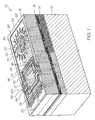
- FIG. 1shows a sectioned, three dimensional view of a nozzle arrangement of an printhead chip, in accordance with the invention, for an inkjet printhead;
- FIG. 2shows a three dimensional view of the nozzle arrangement of FIG. 1 .
- reference numeral 10generally indicates a nozzle arrangement for a first embodiment of an ink jet printhead chip, in accordance with the invention.
- the nozzle arrangement 10is one of a plurality of such nozzle arrangements formed on a silicon wafer substrate 12 to define the printhead chip of the invention. As set out in the background of this specification, a single printhead can contain up to 84 000 such nozzle arrangements. For the purposes of clarity and ease of description, only one nozzle arrangement is described. It is to be appreciated that a person of ordinary skill in the field can readily obtain the printhead chip by simply replicating the nozzle arrangement 10 on the wafer substrate 12 .
- the printhead chipis the product of an integrated circuit fabrication technique.
- each nozzle arrangement 10is the product of a MEMS—based fabrication technique.
- a fabrication techniqueinvolves the deposition of functional layers and sacrificial layers of integrated circuit materials. The functional layers are etched to define various moving components and the sacrificial layers are etched away to release the components.
- fabrication techniquesgenerally involve the replication of a large number of similar components on a single wafer that is subsequently diced to separate the various components from each other. This reinforces the submission that a person of ordinary skill in the field can readily obtain the printhead chip of this invention by replicating the nozzle arrangement 10 .
- An electrical drive circuitry layer 14is positioned on the silicon wafer substrate 12 .
- the electrical drive circuitry layer 14includes CMOS drive circuitry.
- the particular configuration of the CMOS drive circuitryis not important to this description and has therefore been shown schematically in the drawings. Suffice to say that it is connected to a suitable microprocessor and provides electrical current to the nozzle arrangement 10 upon receipt of an enabling signal from said suitable microprocessor.
- An example of a suitable microprocessoris described in the above referenced patents/patent applications. It follows that this level of detail will not be set out in this specification.
- the ink passivation layer 16is positioned on the drive circuitry layer 14 .
- the ink passivation layer 16can be of any suitable material, such as silicon nitride.
- the nozzle arrangement 10includes nozzle chamber walls 18 positioned on the ink passivation layer 16 .
- a roof 20is positioned on the nozzle chamber walls 18 so that the roof 20 and the nozzle chamber walls 18 define a nozzle chamber 22 .
- the nozzle chamber walls 18include a distal end wall 24 , a proximal end wall 26 and a pair of opposed sidewalls 28 .
- An ink ejection port 30is defined in the roof 20 to be in fluid communication with the nozzle chamber 22 .
- the roof 20defines a nozzle rim 32 and a recess 34 positioned about the rim 32 to accommodate ink spread.
- the walls 18 and the roof 20are configured so that the nozzle chamber 22 is rectangular in plan.
- a plurality of ink inlet channels 36are defined through the substrate 12 , the drive circuitry layer 14 and the ink passivation layer 16 .
- the ink inlet channel 36is in fluid communication with the nozzle chamber 18 so that ink can be supplied to the nozzle chamber 18 .
- the nozzle arrangement 10includes a work-transmitting structure in the form of a lever mechanism 38 .
- the lever mechanism 38includes an effort formation 40 , a fulcrum formation 42 and a load formation 44 .
- the fulcrum formation 42is interposed between the effort formation 40 and the load formation 44 .
- the fulcrum formation 42is fast with the ink passivation layer 16 .
- the fulcrum formation 42is composite with a primary layer 46 and a secondary layer 48 .
- the layers 46 , 48are configured so that the fulcrum formation 42 is resiliently deformable to permit pivotal movement of the fulcrum formation 42 with respect to the substrate 12 .
- the layers 46 , 48can be of a number of materials that are used in integrated circuit fabrication.
- TiAlNtitanium aluminum nitride
- TiAlNtitanium aluminum nitride
- the load formation 44defines part of the proximal end wall 26 .
- the load formation 44is composite with a primary layer 50 and a secondary layer 52 .
- the layers 50 , 52can be of any of a number of materials that are used in integrated circuit fabrication.
- the nozzle arrangement 10is fabricated by using successive deposition and etching steps. It follows that it is convenient for the layers 50 , 52 to be of the same material as the layers 46 , 48 . Thus, the layers 50 , 52 can be of TiAlN and titanium, respectively.
- the nozzle arrangement 10includes an ink-ejecting member in the form of an elongate rectangular paddle 54 .
- the paddle 54is fixed to the load formation 44 and extends towards the distal end wall 24 . Further, the paddle 54 is dimensioned to correspond generally with the nozzle chamber 22 . It follows that displacement of the paddle 54 towards and away from the ink ejection port 30 with sufficient energy results in the ejection of an ink drop from the ink ejection port.
- the manner in which drop ejection is achievedis described in detail in the above referenced patents/applications and is therefore not discussed in any detail here.
- the paddle 54is of TiAlN.
- the paddle 54is an extension of the layer 50 of the load formation 44 of the lever mechanism 38 .
- the paddle 54has corrugations 56 to strengthen the paddle 54 against flexure during operation.
- the effort formation 40is also composite with a primary layer 58 and a secondary layer 60 .
- the layers 58 , 60can be of any of a number of materials that are used in integrated circuit fabrication. However, as set out above, the nozzle arrangement 10 is fabricated by using successive deposition and etching steps. It follows that it is convenient for the layers 58 , 60 to be of the same material as the layers 46 , 48 . Thus, the layers 58 , 60 can be of TiAlN and titanium, respectively.
- the nozzle arrangement 10includes an actuator in the form of a thermal bend actuator 62 .
- the thermal bend actuator 62is of a conductive material that is capable of being resistively heated.
- the conductive materialhas a coefficient of thermal expansion that is such that, when heated and subsequently cooled, the material is capable of expansion and contraction to an extent sufficient to perform work on a MEMS scale.
- the thermal bend actuator 62can be any of a number of thermal bend actuators described in the above patents/patent applications.
- the thermal bend actuator 62includes an actuator arm 64 that has an active portion 82 and a passive portion.
- the active portion 82has a pair of inner legs 66 and the passive portion is defined by a leg positioned on each side of the pair of inner legs 66 .
- a bridge portion 68interconnects the active legs 66 and the passive legs.
- Each leg 66is fixed to one of a pair of anchor formations in the form of active anchors 70 that extend from the ink passivation layer 16 .
- Each active anchor 70is configured so that the legs 66 are electrically connected to the drive circuitry layer 14 .
- Each passive legis fixed to one of a pair of anchor formations in the form of passive anchors 88 that are electrically isolated from the drive circuitry layer 14 .
- the legs 66 and the bridge portion 68are configured so that when a current from the drive circuitry layer 14 is set up in the legs 66 , the actuator arm 64 is subjected to differential heating.
- the actuator arm 64is shaped so that the passive legs are interposed between at least a portion of the legs 66 and the substrate 12 . It will be appreciated that this causes the actuator arm 64 to bend towards the substrate 12 .
- the bridge portion 68therefore defines a working end of the actuator 62 .
- the bridge portion 68defines the primary layer 58 of the effort formation 40 .
- the actuator 62is of TiAlN. The Applicant has found this material to be well suited for the actuator 62 .
- the lever mechanism 38includes a lever arm formation 72 positioned on, and fast with, the secondary layers 48 , 52 , 60 of the fulcrum formation 42 , the load formation 44 and the effort formation 40 , respectively.
- reciprocal movement of the actuator 62 towards and away from the substrate 12is converted into reciprocal angular displacement of the paddle 54 via the lever mechanism 38 to eject ink drops from the ink ejection port 30 .
- Each active anchor 70 and passive anchoris also composite with a primary layer 74 and a secondary layer 76 .
- the layers 74 , 76can be of any of a number of materials that are used in integrated circuit fabrication. However, in order to facilitate fabrication, the layer 74 is of TiAlN and the layer 76 is of titanium.
- a cover formation 78is positioned on the anchors 70 , 88 to extend over and to cover the actuator 62 .
- Air chamber walls 90extend between the ink passivation layer 16 and the cover formation 78 so that the cover formation 78 and the air chamber walls 90 define an air chamber 80 .
- the actuator 62 and the anchorsare positioned in the air chamber 80 .
- the cover formation 78 , the lever arm formation 72 and the roof 20are in the form of a unitary protective structure 92 to inhibit damage to the nozzle arrangement 10 .
- the protective structure 92can be one of a number of materials that are used in integrated circuit fabrication. The Applicant has found that silicon dioxide is particularly useful for this task.
- lever arm formation 72it is necessary for the lever arm formation 72 to be displaced relative to the cover formation 78 and the roof 20 . It follows that the cover formation 78 and the lever arm formation 72 are demarcated by a slotted opening 94 in fluid communication with the air chamber 80 . The roof 20 and the lever arm formation 72 are demarcated by a slotted opening 96 in fluid communication with the nozzle chamber 22 .
- the lever arm formation 72 and the roof 20together define ridges 98 that bound the slotted opening 96 .
- the ridges 98define a fluidic seal during ink ejection.
- the ridges 98serve to inhibit ink spreading by providing suitable adhesion surfaces for a meniscus formed by the ink.
- the slotted openings 94 , 96demarcate a torsion formation 100 defined by the protective structure 92 .
- the torsion formation 100serves to support the lever mechanism 38 in position. Further, the torsion formation 100 is configured to experience twisting deformation in order to accommodate pivotal movement of the lever mechanism 38 during operation of the nozzle arrangement 10 .
- the silicon dioxide of the protective structure 92is resiliently flexible on a MEMS scale and is thus suitable for such repetitive distortion.
Landscapes
- Engineering & Computer Science (AREA)
- Manufacturing & Machinery (AREA)
- Multimedia (AREA)
- Signal Processing (AREA)
- Particle Formation And Scattering Control In Inkjet Printers (AREA)
- Facsimile Heads (AREA)
Abstract
Description
| 6,227,652 | 6,213,588 | 6,213,589 | 6,231,163 | 6,247,795 |
| 09/113,099 | 6,244,691 | 6,257,704 | 09/112,778 | 6,220,694 |
| 6,257,705 | 6,247,794 | 6,234,610 | 6,247,793 | 6,264,306 |
| 6,241,342 | 6,247,792 | 6,264,307 | 6,254,220 | 6,234,611 |
| 09/112,808 | 09/112,809 | 6,239,821 | 09/113,083 | 6,247,796 |
| 09/113,122 | 09/112,793 | 09/112,794 | 09/113,128 | 09/113,127 |
| 6,227,653 | 6,234,609 | 6,238,040 | 6,188,415 | 6,227,654 |
| 6,209,989 | 6,247,791 | 09/112,764 | 6,217,153 | 09/112,767 |
| 6,243,113 | 09/112,807 | 6,247,790 | 6,260,953 | 6,267,469 |
| 09/425,419 | 09/425,418 | 09/425,194 | 09/425,193 | 09/422,892 |
| 09/422,806 | 09/425,420 | 09/422,893 | 09/693,703 | 09/693,706 |
| 09/693,313 | 09/693,279 | 09/693,727 | 09/693,708 | 09/575,141 |
| 09/113,053 | 09/855,094 | 09/854,762 | 09/854,715 | 09/854,830 |
| 09/854,714 | 09/854,703 | 09/855,093 | 09/854,815 | 09/854,825 |
| 09/864,377 | 09/864,380 | 09/900,178 | 09/864,379 | 09/864,378 |
| 09/864,334 | 09/864,332 | 09/864,343 | 09/864,342 | 09/866,786 |
| 09/874,757 | 09/900,174 | 09/900,160 | 09/900,175 | 09/900,177 |
| 09/900,159 | 09/900,176 | 09/922,274 | 09/922,275 | 09/922,158 |
| 09/922,159 | 09/922,036 | 09/922,047 | 09/922,029 | 09/922,207 |
| 09/922,112 | 09/922,105 | 09/942,549 | 09/942,605 | 09/942,548 |
| 09/942,603 | 09/942,604 | |||
Claims (11)
Priority Applications (27)
| Application Number | Priority Date | Filing Date | Title |
|---|---|---|---|
| US10/120,346US6582059B2 (en) | 1997-07-15 | 2002-04-12 | Discrete air and nozzle chambers in a printhead chip for an inkjet printhead |
| EP02759893AEP1494866B1 (en) | 2002-04-12 | 2002-08-29 | Discrete air and nozzle chambers in a printhead chip for an inkjet printhead |
| US10/510,154US7334873B2 (en) | 2002-04-12 | 2002-08-29 | Discrete air and nozzle chambers in a printhead chip for an inkjet printhead |
| DE60230549TDE60230549D1 (en) | 2002-04-12 | 2002-08-29 | DISCRETE AIR AND JET CHAMBERS IN A PRINT HEAD CHIP FOR AN INK JET PRINT HEAD |
| AT02759893TATE418455T1 (en) | 2002-04-12 | 2002-08-29 | DISCRETE AIR AND NOZZLE CHAMBERS IN A PRINTHEAD CHIP FOR AN INKJET PRINTHEAD |
| AU2002325640AAU2002325640B2 (en) | 2002-04-12 | 2002-08-29 | Discrete air and nozzle chambers in a printhead chip for an inkjet printhead |
| CNB028287169ACN100402290C (en) | 2002-04-12 | 2002-08-29 | Printhead die for inkjet printhead having nozzle chamber and discrete air chamber |
| PCT/AU2002/001169WO2003086766A1 (en) | 2002-04-12 | 2002-08-29 | Discrete air and nozzle chambers in a printhead chip for an inkjet printhead |
| KR1020047016256AKR100643659B1 (en) | 2002-04-12 | 2002-08-29 | Printhead Chip for Inkjet Printheads with Separated Air and Nozzle Chambers |
| US10/302,556US6666543B2 (en) | 1997-07-15 | 2002-11-23 | Printhead chip that incorporates covering formations for actuators of the printhead chip |
| US10/949,347US7004566B2 (en) | 1997-07-15 | 2004-09-27 | Inkjet printhead chip that incorporates micro-mechanical lever mechanisms |
| IL164448AIL164448A (en) | 2002-04-12 | 2004-10-05 | Discrete air and nozzle chambers in a printhead chip for an inkjet printhead |
| ZA200408147AZA200408147B (en) | 2002-04-12 | 2004-10-08 | Discrete air and nozzle chambers in a printhead chip for an inkjet printhead. |
| US10/962,394US6948799B2 (en) | 1997-07-15 | 2004-10-13 | Micro-electromechanical fluid ejecting device that incorporates a covering formation for a micro-electromechanical actuator |
| US10/982,787US7055933B2 (en) | 1997-07-15 | 2004-11-08 | MEMS device having formations for covering actuators of the device |
| US11/144,815US7111925B2 (en) | 1997-07-15 | 2005-06-06 | Inkjet printhead integrated circuit |
| US11/172,810US7055935B2 (en) | 1997-07-15 | 2005-07-05 | Ink ejection devices within an inkjet printer |
| US11/329,143US7147305B2 (en) | 1997-07-15 | 2006-01-11 | Printer formed from integrated circuit printhead |
| US11/442,179US7246884B2 (en) | 1997-07-15 | 2006-05-30 | Inkjet printhead having enclosed inkjet actuators |
| US11/584,619US7278711B2 (en) | 1997-07-15 | 2006-10-23 | Nozzle arrangement incorporating a lever based ink displacement mechanism |
| US11/766,025US7556356B1 (en) | 1997-07-15 | 2007-06-20 | Inkjet printhead integrated circuit with ink spread prevention |
| US11/860,420US7506965B2 (en) | 1997-07-15 | 2007-09-24 | Inkjet printhead integrated circuit with work transmitting structures |
| US12/015,483US7771017B2 (en) | 1997-07-15 | 2008-01-16 | Nozzle arrangement for an inkjet printhead incorporating a protective structure |
| US12/368,993US7866797B2 (en) | 1997-07-15 | 2009-02-10 | Inkjet printhead integrated circuit |
| US12/482,417US7942503B2 (en) | 1997-07-15 | 2009-06-10 | Printhead with nozzle face recess to contain ink floods |
| US12/848,971US20100295902A1 (en) | 1997-07-15 | 2010-08-02 | Nozzle arrangement for inkjet printhead incorporating a protective structure |
| US13/079,006US8113629B2 (en) | 1997-07-15 | 2011-04-03 | Inkjet printhead integrated circuit incorporating fulcrum assisted ink ejection actuator |
Applications Claiming Priority (6)
| Application Number | Priority Date | Filing Date | Title |
|---|---|---|---|
| AUPO7991AAUPO799197A0 (en) | 1997-07-15 | 1997-07-15 | Image processing method and apparatus (ART01) |
| AUPO7991 | 1997-07-15 | ||
| AUPO259298 | 1998-03-25 | ||
| AUPO2592 | 1998-03-25 | ||
| US09/112,767US6416167B1 (en) | 1997-07-15 | 1998-07-10 | Thermally actuated ink jet printing mechanism having a series of thermal actuator units |
| US10/120,346US6582059B2 (en) | 1997-07-15 | 2002-04-12 | Discrete air and nozzle chambers in a printhead chip for an inkjet printhead |
Related Parent Applications (1)
| Application Number | Title | Priority Date | Filing Date |
|---|---|---|---|
| US09/112,767Continuation-In-PartUS6416167B1 (en) | 1997-07-15 | 1998-07-10 | Thermally actuated ink jet printing mechanism having a series of thermal actuator units |
Related Child Applications (5)
| Application Number | Title | Priority Date | Filing Date |
|---|---|---|---|
| US10/510,154ContinuationUS7334873B2 (en) | 1997-07-15 | 2002-08-29 | Discrete air and nozzle chambers in a printhead chip for an inkjet printhead |
| PCT/AU2002/001169ContinuationWO2003086766A1 (en) | 1997-07-15 | 2002-08-29 | Discrete air and nozzle chambers in a printhead chip for an inkjet printhead |
| US10510154Continuation | 2002-08-29 | ||
| US10/302,566ContinuationUS6849411B2 (en) | 1997-04-04 | 2002-11-22 | Microfluidic sequencing methods |
| US10/302,556ContinuationUS6666543B2 (en) | 1997-07-15 | 2002-11-23 | Printhead chip that incorporates covering formations for actuators of the printhead chip |
Publications (2)
| Publication Number | Publication Date |
|---|---|
| US20020149648A1 US20020149648A1 (en) | 2002-10-17 |
| US6582059B2true US6582059B2 (en) | 2003-06-24 |
Family
ID=29248275
Family Applications (5)
| Application Number | Title | Priority Date | Filing Date |
|---|---|---|---|
| US10/120,346Expired - Fee RelatedUS6582059B2 (en) | 1997-07-15 | 2002-04-12 | Discrete air and nozzle chambers in a printhead chip for an inkjet printhead |
| US10/510,154Expired - Fee RelatedUS7334873B2 (en) | 1997-07-15 | 2002-08-29 | Discrete air and nozzle chambers in a printhead chip for an inkjet printhead |
| US10/302,556Expired - Fee RelatedUS6666543B2 (en) | 1997-07-15 | 2002-11-23 | Printhead chip that incorporates covering formations for actuators of the printhead chip |
| US12/015,483Expired - Fee RelatedUS7771017B2 (en) | 1997-07-15 | 2008-01-16 | Nozzle arrangement for an inkjet printhead incorporating a protective structure |
| US12/848,971AbandonedUS20100295902A1 (en) | 1997-07-15 | 2010-08-02 | Nozzle arrangement for inkjet printhead incorporating a protective structure |
Family Applications After (4)
| Application Number | Title | Priority Date | Filing Date |
|---|---|---|---|
| US10/510,154Expired - Fee RelatedUS7334873B2 (en) | 1997-07-15 | 2002-08-29 | Discrete air and nozzle chambers in a printhead chip for an inkjet printhead |
| US10/302,556Expired - Fee RelatedUS6666543B2 (en) | 1997-07-15 | 2002-11-23 | Printhead chip that incorporates covering formations for actuators of the printhead chip |
| US12/015,483Expired - Fee RelatedUS7771017B2 (en) | 1997-07-15 | 2008-01-16 | Nozzle arrangement for an inkjet printhead incorporating a protective structure |
| US12/848,971AbandonedUS20100295902A1 (en) | 1997-07-15 | 2010-08-02 | Nozzle arrangement for inkjet printhead incorporating a protective structure |
Country Status (10)
| Country | Link |
|---|---|
| US (5) | US6582059B2 (en) |
| EP (1) | EP1494866B1 (en) |
| KR (1) | KR100643659B1 (en) |
| CN (1) | CN100402290C (en) |
| AT (1) | ATE418455T1 (en) |
| AU (1) | AU2002325640B2 (en) |
| DE (1) | DE60230549D1 (en) |
| IL (1) | IL164448A (en) |
| WO (1) | WO2003086766A1 (en) |
| ZA (1) | ZA200408147B (en) |
Cited By (21)
| Publication number | Priority date | Publication date | Assignee | Title |
|---|---|---|---|---|
| US20050140747A1 (en)* | 2003-12-30 | 2005-06-30 | Batterton John C. | Drop ejection assembly |
| US20050146569A1 (en)* | 2003-12-30 | 2005-07-07 | Hoisington Paul A. | Drop ejection assembly |
| US20050146561A1 (en)* | 2003-12-30 | 2005-07-07 | Andreas Bibl | Drop ejection assembly |
| US20050146560A1 (en)* | 2003-12-30 | 2005-07-07 | Barss Steven H. | Drop ejection assembly |
| US7052117B2 (en) | 2002-07-03 | 2006-05-30 | Dimatix, Inc. | Printhead having a thin pre-fired piezoelectric layer |
| US20080012905A1 (en)* | 1997-07-15 | 2008-01-17 | Silverbrook Research Pty Ltd | Inkjet printhead integrated circuit with work transmitting structures |
| US20080111861A1 (en)* | 1997-07-15 | 2008-05-15 | Silverbrook Research Pty Ltd | Nozzle Arrangement For An Inkjet Printhead Incorporating A Protective Structure |
| US20090244184A1 (en)* | 1997-07-15 | 2009-10-01 | Silverbrook Research Pty Ltd | Printhead With Nozzle Face Recess To Contain Ink Floods |
| US7950777B2 (en) | 1997-07-15 | 2011-05-31 | Silverbrook Research Pty Ltd | Ejection nozzle assembly |
| US7988247B2 (en) | 2007-01-11 | 2011-08-02 | Fujifilm Dimatix, Inc. | Ejection of drops having variable drop size from an ink jet printer |
| US8020970B2 (en) | 1997-07-15 | 2011-09-20 | Silverbrook Research Pty Ltd | Printhead nozzle arrangements with magnetic paddle actuators |
| US8025366B2 (en) | 1997-07-15 | 2011-09-27 | Silverbrook Research Pty Ltd | Inkjet printhead with nozzle layer defining etchant holes |
| US8029101B2 (en) | 1997-07-15 | 2011-10-04 | Silverbrook Research Pty Ltd | Ink ejection mechanism with thermal actuator coil |
| US8029102B2 (en) | 1997-07-15 | 2011-10-04 | Silverbrook Research Pty Ltd | Printhead having relatively dimensioned ejection ports and arms |
| US8061812B2 (en) | 1997-07-15 | 2011-11-22 | Silverbrook Research Pty Ltd | Ejection nozzle arrangement having dynamic and static structures |
| US8075104B2 (en) | 1997-07-15 | 2011-12-13 | Sliverbrook Research Pty Ltd | Printhead nozzle having heater of higher resistance than contacts |
| US8083326B2 (en) | 1997-07-15 | 2011-12-27 | Silverbrook Research Pty Ltd | Nozzle arrangement with an actuator having iris vanes |
| US8123336B2 (en) | 1997-07-15 | 2012-02-28 | Silverbrook Research Pty Ltd | Printhead micro-electromechanical nozzle arrangement with motion-transmitting structure |
| US8459768B2 (en) | 2004-03-15 | 2013-06-11 | Fujifilm Dimatix, Inc. | High frequency droplet ejection device and method |
| US8491076B2 (en) | 2004-03-15 | 2013-07-23 | Fujifilm Dimatix, Inc. | Fluid droplet ejection devices and methods |
| US8708441B2 (en) | 2004-12-30 | 2014-04-29 | Fujifilm Dimatix, Inc. | Ink jet printing |
Families Citing this family (14)
| Publication number | Priority date | Publication date | Assignee | Title |
|---|---|---|---|---|
| US20040130599A1 (en)* | 1997-07-15 | 2004-07-08 | Silverbrook Research Pty Ltd | Ink jet printhead with amorphous ceramic chamber |
| US7011390B2 (en)* | 1997-07-15 | 2006-03-14 | Silverbrook Research Pty Ltd | Printing mechanism having wide format printing zone |
| US6840600B2 (en)* | 1997-07-15 | 2005-01-11 | Silverbrook Research Pty Ltd | Fluid ejection device that incorporates covering formations for actuators of the fluid ejection device |
| US7004566B2 (en)* | 1997-07-15 | 2006-02-28 | Silverbrook Research Pty Ltd | Inkjet printhead chip that incorporates micro-mechanical lever mechanisms |
| AUPP653998A0 (en)* | 1998-10-16 | 1998-11-05 | Silverbrook Research Pty Ltd | Micromechanical device and method (ij46B) |
| US7131715B2 (en)* | 1997-07-15 | 2006-11-07 | Silverbrook Research Pty Ltd | Printhead chip that incorporates micro-mechanical lever mechanisms |
| US20110228008A1 (en)* | 1997-07-15 | 2011-09-22 | Silverbrook Research Pty Ltd | Printhead having relatively sized fluid ducts and nozzles |
| US7246884B2 (en)* | 1997-07-15 | 2007-07-24 | Silverbrook Research Pty Ltd | Inkjet printhead having enclosed inkjet actuators |
| US7111925B2 (en)* | 1997-07-15 | 2006-09-26 | Silverbrook Research Pty Ltd | Inkjet printhead integrated circuit |
| US7008046B2 (en)* | 1997-07-15 | 2006-03-07 | Silverbrook Research Pty Ltd | Micro-electromechanical liquid ejection device |
| US6834939B2 (en)* | 2002-11-23 | 2004-12-28 | Silverbrook Research Pty Ltd | Micro-electromechanical device that incorporates covering formations for actuators of the device |
| TWI306415B (en)* | 2006-12-19 | 2009-02-21 | Ind Tech Res Inst | Inkjet dispensing apparatus |
| CN104080609B (en)* | 2012-04-19 | 2016-05-25 | 惠普发展公司,有限责任合伙企业 | Inkjet problem determination |
| US9205651B2 (en)* | 2014-01-21 | 2015-12-08 | Xerox Corporation | Subtractive three dimensional fabrication of an inkjet plate |
Citations (3)
| Publication number | Priority date | Publication date | Assignee | Title |
|---|---|---|---|---|
| WO2000023279A1 (en) | 1998-10-16 | 2000-04-27 | Silverbrook Research Pty. Limited | Improvements relating to inkjet printers |
| WO2001089839A1 (en) | 2000-05-23 | 2001-11-29 | Silverbrook Research Pty. Ltd. | Ink jet printhead having a moving nozzle with an externally arranged actuator |
| US6425651B1 (en) | 1997-07-15 | 2002-07-30 | Silverbrook Research Pty Ltd | High-density inkjet nozzle array for an inkjet printhead |
Family Cites Families (127)
| Publication number | Priority date | Publication date | Assignee | Title |
|---|---|---|---|---|
| GB792145A (en) | 1953-05-20 | 1958-03-19 | Technograph Printed Circuits L | Improvements in and relating to devices for obtaining a mechanical movement from theaction of an electric current |
| DE1648322A1 (en) | 1967-07-20 | 1971-03-25 | Vdo Schindling | Measuring or switching element made of bimetal |
| FR2188389B1 (en) | 1972-06-08 | 1975-06-13 | Cibie Projecteurs | |
| FR2231076A2 (en) | 1973-05-24 | 1974-12-20 | Electricite De France | Driving organ operated by thermal means - esp. for use in corrosive or dangerous environments formed by two metal strips |
| DE2905063A1 (en) | 1979-02-10 | 1980-08-14 | Olympia Werke Ag | Ink nozzle air intake avoidance system - has vibratory pressure generator shutting bore in membrane in rest position |
| JPS55123476A (en)* | 1979-03-19 | 1980-09-22 | Hitachi Ltd | Multinozzle ink jetting recorder |
| JPS58112747A (en) | 1981-12-26 | 1983-07-05 | Fujitsu Ltd | Inkjet recording device |
| JPS58116165A (en) | 1981-12-29 | 1983-07-11 | Canon Inc | Ink injection head |
| DE3214791A1 (en) | 1982-04-21 | 1983-10-27 | Siemens AG, 1000 Berlin und 8000 München | WRITING DEVICE WORKING WITH LIQUID DROPS |
| US4423401A (en)* | 1982-07-21 | 1983-12-27 | Tektronix, Inc. | Thin-film electrothermal device |
| DE3245283A1 (en) | 1982-12-07 | 1984-06-07 | Siemens AG, 1000 Berlin und 8000 München | Arrangement for expelling liquid droplets |
| US4553393A (en)* | 1983-08-26 | 1985-11-19 | The United States Of America As Represented By The Administrator Of The National Aeronautics And Space Administration | Memory metal actuator |
| JPS6125849A (en) | 1984-07-17 | 1986-02-04 | Canon Inc | Inkjet recording device |
| DE3430155A1 (en) | 1984-08-16 | 1986-02-27 | Siemens AG, 1000 Berlin und 8000 München | Indirectly heated bimetal |
| JPS61106259A (en)* | 1984-10-31 | 1986-05-24 | Hitachi Ltd | ink droplet ejecting device |
| SE447222B (en)* | 1984-12-21 | 1986-11-03 | Swedot System Ab | ELECTROMAGNETIC MANOVERABLE VALVE DEVICE, SPECIFICALLY FOR GENERATING DROPS IN A HYDRAULIC PRINTER |
| JPS61268453A (en) | 1985-05-23 | 1986-11-27 | Olympus Optical Co Ltd | Ink jet printer head |
| US5258774A (en)* | 1985-11-26 | 1993-11-02 | Dataproducts Corporation | Compensation for aerodynamic influences in ink jet apparatuses having ink jet chambers utilizing a plurality of orifices |
| DE3716996A1 (en) | 1987-05-21 | 1988-12-08 | Vdo Schindling | Deformation element |
| JPH01105746A (en) | 1987-10-19 | 1989-04-24 | Ricoh Co Ltd | Ink jet head |
| JPH01115639A (en) | 1987-10-30 | 1989-05-08 | Ricoh Co Ltd | inkjet recording head |
| JPH01128839A (en) | 1987-11-13 | 1989-05-22 | Ricoh Co Ltd | inkjet recording head |
| JPH01257058A (en) | 1988-04-07 | 1989-10-13 | Seiko Epson Corp | Ink jet head |
| DE3814150A1 (en)* | 1988-04-27 | 1989-11-09 | Draegerwerk Ag | VALVE ARRANGEMENT MADE FROM MICROSTRUCTURED COMPONENTS |
| JPH01306254A (en) | 1988-06-03 | 1989-12-11 | Seiko Epson Corp | inkjet head |
| JPH0250841A (en) | 1988-08-12 | 1990-02-20 | Seiko Epson Corp | inkjet head |
| JPH0292643A (en) | 1988-09-30 | 1990-04-03 | Seiko Epson Corp | inkjet head |
| IT1229927B (en) | 1988-10-14 | 1991-09-16 | Cipelletti Alberto Cae | VANE PUMP. |
| JPH02108544A (en) | 1988-10-19 | 1990-04-20 | Seiko Epson Corp | inkjet print head |
| US4864824A (en)* | 1988-10-31 | 1989-09-12 | American Telephone And Telegraph Company, At&T Bell Laboratories | Thin film shape memory alloy and method for producing |
| JP2697041B2 (en) | 1988-12-10 | 1998-01-14 | ミノルタ株式会社 | Inkjet printer |
| JPH02162049A (en) | 1988-12-16 | 1990-06-21 | Seiko Epson Corp | printer head |
| JPH041051A (en) | 1989-02-22 | 1992-01-06 | Ricoh Co Ltd | inkjet recording device |
| JPH02265752A (en) | 1989-04-05 | 1990-10-30 | Matsushita Electric Ind Co Ltd | Ink-jet recording head |
| EP0398031A1 (en)* | 1989-04-19 | 1990-11-22 | Seiko Epson Corporation | Ink jet head |
| JPH0365348A (en) | 1989-08-04 | 1991-03-20 | Matsushita Electric Ind Co Ltd | Ink jet head |
| JP2746703B2 (en) | 1989-11-09 | 1998-05-06 | 松下電器産業株式会社 | Ink jet head device and method of manufacturing the same |
| JPH03112662A (en) | 1989-09-27 | 1991-05-14 | Seiko Epson Corp | Ink jet printer |
| JP2964618B2 (en) | 1989-11-10 | 1999-10-18 | セイコーエプソン株式会社 | Head for inkjet printer |
| JPH03180350A (en) | 1989-12-08 | 1991-08-06 | Seiko Epson Corp | Ink jet head |
| JPH04118241A (en) | 1990-09-10 | 1992-04-20 | Seiko Epson Corp | Amplitude conversion actuator for inkjet printer head |
| JPH04126255A (en) | 1990-09-18 | 1992-04-27 | Seiko Epson Corp | inkjet head |
| JPH04141429A (en) | 1990-10-03 | 1992-05-14 | Seiko Epson Corp | Ink jet head |
| DE4031248A1 (en) | 1990-10-04 | 1992-04-09 | Kernforschungsz Karlsruhe | MICROMECHANICAL ELEMENT |
| US6019457A (en)* | 1991-01-30 | 2000-02-01 | Canon Information Systems Research Australia Pty Ltd. | Ink jet print device and print head or print apparatus using the same |
| US5126755A (en) | 1991-03-26 | 1992-06-30 | Videojet Systems International, Inc. | Print head assembly for ink jet printer |
| US5164740A (en) | 1991-04-24 | 1992-11-17 | Yehuda Ivri | High frequency printing mechanism |
| JPH04353458A (en) | 1991-05-31 | 1992-12-08 | Brother Ind Ltd | Ink jet head |
| JPH04368851A (en) | 1991-06-17 | 1992-12-21 | Seiko Epson Corp | Magnetic field generating substrate and ink jet head equipped therewith |
| JPH0528765A (en) | 1991-07-18 | 1993-02-05 | Nec Home Electron Ltd | Memory control circuit |
| GB9121851D0 (en) | 1991-10-15 | 1991-11-27 | Willett Int Ltd | Device |
| JP3450349B2 (en) | 1992-03-31 | 2003-09-22 | キヤノン株式会社 | Cantilever probe |
| JPH05318724A (en) | 1992-05-19 | 1993-12-03 | Seikosha Co Ltd | Ink jet recorder |
| JPH0691868A (en) | 1992-09-11 | 1994-04-05 | Brother Ind Ltd | Driving circuit of piezo-electric transducer in liquid drop spraying device |
| JPH0691865A (en) | 1992-09-17 | 1994-04-05 | Seikosha Co Ltd | Ink jet head |
| JP2615319B2 (en) | 1992-09-17 | 1997-05-28 | セイコープレシジョン株式会社 | Inkjet head |
| US5387314A (en)* | 1993-01-25 | 1995-02-07 | Hewlett-Packard Company | Fabrication of ink fill slots in thermal ink-jet printheads utilizing chemical micromachining |
| GB9302170D0 (en) | 1993-02-04 | 1993-03-24 | Domino Printing Sciences Plc | Ink jet printer |
| IT1270861B (en) | 1993-05-31 | 1997-05-13 | Olivetti Canon Ind Spa | IMPROVED INK JET HEAD FOR A POINT PRINTER |
| US5666141A (en) | 1993-07-13 | 1997-09-09 | Sharp Kabushiki Kaisha | Ink jet head and a method of manufacturing thereof |
| DE4328433A1 (en) | 1993-08-24 | 1995-03-02 | Heidelberger Druckmasch Ag | Ink jet spray method, and ink jet spray device |
| DE19516997C2 (en) | 1994-05-10 | 1998-02-26 | Sharp Kk | Ink jet head and method of manufacturing the same |
| JPH07314665A (en) | 1994-05-27 | 1995-12-05 | Canon Inc | Inkjet recording head, recording apparatus and recording method using the same |
| JPH07314673A (en) | 1994-05-27 | 1995-12-05 | Sharp Corp | Inkjet head |
| JP3515830B2 (en)* | 1994-07-14 | 2004-04-05 | 富士写真フイルム株式会社 | Method of manufacturing ink jet recording head chip, method of manufacturing ink jet recording head, and recording apparatus |
| JPH0890769A (en) | 1994-09-27 | 1996-04-09 | Sharp Corp | Diaphragm type inkjet head with folds |
| JPH08142323A (en) | 1994-11-24 | 1996-06-04 | Sharp Corp | Inkjet head and manufacturing method thereof |
| TW365578B (en) | 1995-04-14 | 1999-08-01 | Canon Kk | Liquid ejecting head, liquid ejecting device and liquid ejecting method |
| AU712741B2 (en)* | 1995-04-26 | 1999-11-18 | Canon Kabushiki Kaisha | Liquid ejecting head, liquid ejecting device and liquid ejecting method |
| JPH08336965A (en) | 1995-06-14 | 1996-12-24 | Sharp Corp | Inkjet head |
| DE69617540T2 (en) | 1995-06-28 | 2002-05-23 | Canon K.K., Tokio/Tokyo | Micro device for liquid jet recording head equipped therewith, liquid jet recording device with this liquid jet recording head |
| US5828394A (en) | 1995-09-20 | 1998-10-27 | The Board Of Trustees Of The Leland Stanford Junior University | Fluid drop ejector and method |
| JPH09104109A (en) | 1995-10-12 | 1997-04-22 | Sharp Corp | Inkjet head and manufacturing method thereof |
| JPH09314915A (en) | 1996-05-31 | 1997-12-09 | Canon Inc | Printing control device, printing device control method, printing system, and storage medium |
| JP3653348B2 (en) | 1996-08-23 | 2005-05-25 | 三洋電機株式会社 | Air conditioner |
| JPH10124268A (en)* | 1996-08-30 | 1998-05-15 | Canon Inc | Printing control device |
| AUPO799197A0 (en)* | 1997-07-15 | 1997-08-07 | Silverbrook Research Pty Ltd | Image processing method and apparatus (ART01) |
| TW429218B (en) | 1997-06-06 | 2001-04-11 | Canon Kk | A liquid discharging method, a liquid discharge head, and a liquid discharge apparatus |
| US6672706B2 (en)* | 1997-07-15 | 2004-01-06 | Silverbrook Research Pty Ltd | Wide format pagewidth inkjet printer |
| US6834939B2 (en)* | 2002-11-23 | 2004-12-28 | Silverbrook Research Pty Ltd | Micro-electromechanical device that incorporates covering formations for actuators of the device |
| US6652052B2 (en)* | 1997-07-15 | 2003-11-25 | Silverbrook Research Pty Ltd | Processing of images for high volume pagewidth printing |
| US6712453B2 (en)* | 1997-07-15 | 2004-03-30 | Silverbrook Research Pty Ltd. | Ink jet nozzle rim |
| US6460971B2 (en)* | 1997-07-15 | 2002-10-08 | Silverbrook Research Pty Ltd | Ink jet with high young's modulus actuator |
| US7556356B1 (en)* | 1997-07-15 | 2009-07-07 | Silverbrook Research Pty Ltd | Inkjet printhead integrated circuit with ink spread prevention |
| US7004566B2 (en)* | 1997-07-15 | 2006-02-28 | Silverbrook Research Pty Ltd | Inkjet printhead chip that incorporates micro-mechanical lever mechanisms |
| US20040130599A1 (en)* | 1997-07-15 | 2004-07-08 | Silverbrook Research Pty Ltd | Ink jet printhead with amorphous ceramic chamber |
| AUPP398798A0 (en)* | 1998-06-09 | 1998-07-02 | Silverbrook Research Pty Ltd | Image creation method and apparatus (ij43) |
| US6814429B2 (en)* | 1997-07-15 | 2004-11-09 | Silverbrook Research Pty Ltd | Ink jet printhead incorporating a backflow prevention mechanism |
| US6682174B2 (en)* | 1998-03-25 | 2004-01-27 | Silverbrook Research Pty Ltd | Ink jet nozzle arrangement configuration |
| US7337532B2 (en)* | 1997-07-15 | 2008-03-04 | Silverbrook Research Pty Ltd | Method of manufacturing micro-electromechanical device having motion-transmitting structure |
| US6582059B2 (en)* | 1997-07-15 | 2003-06-24 | Silverbrook Research Pty Ltd | Discrete air and nozzle chambers in a printhead chip for an inkjet printhead |
| US7011390B2 (en)* | 1997-07-15 | 2006-03-14 | Silverbrook Research Pty Ltd | Printing mechanism having wide format printing zone |
| US6648453B2 (en)* | 1997-07-15 | 2003-11-18 | Silverbrook Research Pty Ltd | Ink jet printhead chip with predetermined micro-electromechanical systems height |
| US7753463B2 (en)* | 1997-07-15 | 2010-07-13 | Silverbrook Research Pty Ltd | Processing of images for high volume pagewidth printing |
| US6485123B2 (en)* | 1997-07-15 | 2002-11-26 | Silverbrook Research Pty Ltd | Shutter ink jet |
| US6180427B1 (en)* | 1997-07-15 | 2001-01-30 | Silverbrook Research Pty. Ltd. | Method of manufacture of a thermally actuated ink jet including a tapered heater element |
| US6471336B2 (en)* | 1997-07-15 | 2002-10-29 | Silverbrook Research Pty Ltd. | Nozzle arrangement that incorporates a reversible actuating mechanism |
| US7468139B2 (en)* | 1997-07-15 | 2008-12-23 | Silverbrook Research Pty Ltd | Method of depositing heater material over a photoresist scaffold |
| AUPP089397A0 (en)* | 1997-12-12 | 1998-01-08 | Silverbrook Research Pty Ltd | Image creation method and apparatus (IJ37) |
| AUPP653998A0 (en)* | 1998-10-16 | 1998-11-05 | Silverbrook Research Pty Ltd | Micromechanical device and method (ij46B) |
| US6935724B2 (en)* | 1997-07-15 | 2005-08-30 | Silverbrook Research Pty Ltd | Ink jet nozzle having actuator with anchor positioned between nozzle chamber and actuator connection point |
| US6880918B2 (en)* | 1997-07-15 | 2005-04-19 | Silverbrook Research Pty Ltd | Micro-electromechanical device that incorporates a motion-transmitting structure |
| US7195339B2 (en)* | 1997-07-15 | 2007-03-27 | Silverbrook Research Pty Ltd | Ink jet nozzle assembly with a thermal bend actuator |
| US6283582B1 (en)* | 1997-07-15 | 2001-09-04 | Silverbrook Research Pty Ltd | Iris motion ink jet printing mechanism |
| US6540332B2 (en)* | 1997-07-15 | 2003-04-01 | Silverbrook Research Pty Ltd | Motion transmitting structure for a nozzle arrangement of a printhead chip for an inkjet printhead |
| US6682176B2 (en)* | 1997-07-15 | 2004-01-27 | Silverbrook Research Pty Ltd | Ink jet printhead chip with nozzle arrangements incorporating spaced actuating arms |
| US7465030B2 (en)* | 1997-07-15 | 2008-12-16 | Silverbrook Research Pty Ltd | Nozzle arrangement with a magnetic field generator |
| US6840600B2 (en)* | 1997-07-15 | 2005-01-11 | Silverbrook Research Pty Ltd | Fluid ejection device that incorporates covering formations for actuators of the fluid ejection device |
| US6213589B1 (en)* | 1997-07-15 | 2001-04-10 | Silverbrook Research Pty Ltd. | Planar thermoelastic bend actuator ink jet printing mechanism |
| US6188415B1 (en)* | 1997-07-15 | 2001-02-13 | Silverbrook Research Pty Ltd | Ink jet printer having a thermal actuator comprising an external coil spring |
| US6416167B1 (en)* | 1997-07-15 | 2002-07-09 | Silverbrook Research Pty Ltd | Thermally actuated ink jet printing mechanism having a series of thermal actuator units |
| US6886917B2 (en)* | 1998-06-09 | 2005-05-03 | Silverbrook Research Pty Ltd | Inkjet printhead nozzle with ribbed wall actuator |
| EP1121249B1 (en)* | 1998-10-16 | 2007-07-25 | Silverbrook Research Pty. Limited | Process of forming a nozzle for an inkjet printhead |
| AUPP702498A0 (en)* | 1998-11-09 | 1998-12-03 | Silverbrook Research Pty Ltd | Image creation method and apparatus (ART77) |
| JP2000293335A (en) | 1999-04-06 | 2000-10-20 | Seiko Epson Corp | Image processing method and image processing system |
| AUPQ131099A0 (en)* | 1999-06-30 | 1999-07-22 | Silverbrook Research Pty Ltd | A method and apparatus (IJ47V8) |
| US6398343B2 (en)* | 2000-05-23 | 2002-06-04 | Silverbrook Research Pty Ltd | Residue guard for nozzle groups of an ink jet printhead |
| US6977751B1 (en)* | 2000-06-30 | 2005-12-20 | Silverbrook Research Pty Ltd | Print engine/controller to work in multiples and a printhead driven by multiple print engine/controllers |
| US6425661B1 (en)* | 2000-06-30 | 2002-07-30 | Silverbrook Research Pty Ltd | Ink cartridge |
| US6561627B2 (en)* | 2000-11-30 | 2003-05-13 | Eastman Kodak Company | Thermal actuator |
| KR20050019802A (en)* | 2002-06-28 | 2005-03-03 | 실버브룩 리서치 피티와이 리미티드 | Ink jet nozzle assembly including displaceable ink pusher |
| US6644786B1 (en)* | 2002-07-08 | 2003-11-11 | Eastman Kodak Company | Method of manufacturing a thermally actuated liquid control device |
| US6685303B1 (en)* | 2002-08-14 | 2004-02-03 | Eastman Kodak Company | Thermal actuator with reduced temperature extreme and method of operating same |
| US6755509B2 (en)* | 2002-11-23 | 2004-06-29 | Silverbrook Research Pty Ltd | Thermal ink jet printhead with suspended beam heater |
| US6719406B1 (en)* | 2002-11-23 | 2004-04-13 | Silverbrook Research Pty Ltd | Ink jet printhead with conformally coated heater |
| US7455023B2 (en)* | 2004-10-22 | 2008-11-25 | Gerstenberger Peter J | Vessel hull protection device |
| US7875426B2 (en)* | 2005-02-04 | 2011-01-25 | University Of South Florida | DNA biochip and methods of use |
- 2002
- 2002-04-12USUS10/120,346patent/US6582059B2/ennot_activeExpired - Fee Related
- 2002-08-29WOPCT/AU2002/001169patent/WO2003086766A1/ennot_activeApplication Discontinuation
- 2002-08-29CNCNB028287169Apatent/CN100402290C/ennot_activeExpired - Fee Related
- 2002-08-29ATAT02759893Tpatent/ATE418455T1/ennot_activeIP Right Cessation
- 2002-08-29DEDE60230549Tpatent/DE60230549D1/ennot_activeExpired - Lifetime
- 2002-08-29EPEP02759893Apatent/EP1494866B1/ennot_activeExpired - Lifetime
- 2002-08-29USUS10/510,154patent/US7334873B2/ennot_activeExpired - Fee Related
- 2002-08-29KRKR1020047016256Apatent/KR100643659B1/ennot_activeExpired - Fee Related
- 2002-08-29AUAU2002325640Apatent/AU2002325640B2/ennot_activeCeased
- 2002-11-23USUS10/302,556patent/US6666543B2/ennot_activeExpired - Fee Related
- 2004
- 2004-10-05ILIL164448Apatent/IL164448A/ennot_activeIP Right Cessation
- 2004-10-08ZAZA200408147Apatent/ZA200408147B/enunknown
- 2008
- 2008-01-16USUS12/015,483patent/US7771017B2/ennot_activeExpired - Fee Related
- 2010
- 2010-08-02USUS12/848,971patent/US20100295902A1/ennot_activeAbandoned
Patent Citations (3)
| Publication number | Priority date | Publication date | Assignee | Title |
|---|---|---|---|---|
| US6425651B1 (en) | 1997-07-15 | 2002-07-30 | Silverbrook Research Pty Ltd | High-density inkjet nozzle array for an inkjet printhead |
| WO2000023279A1 (en) | 1998-10-16 | 2000-04-27 | Silverbrook Research Pty. Limited | Improvements relating to inkjet printers |
| WO2001089839A1 (en) | 2000-05-23 | 2001-11-29 | Silverbrook Research Pty. Ltd. | Ink jet printhead having a moving nozzle with an externally arranged actuator |
Cited By (38)
| Publication number | Priority date | Publication date | Assignee | Title |
|---|---|---|---|---|
| US8061812B2 (en) | 1997-07-15 | 2011-11-22 | Silverbrook Research Pty Ltd | Ejection nozzle arrangement having dynamic and static structures |
| US8075104B2 (en) | 1997-07-15 | 2011-12-13 | Sliverbrook Research Pty Ltd | Printhead nozzle having heater of higher resistance than contacts |
| US8123336B2 (en) | 1997-07-15 | 2012-02-28 | Silverbrook Research Pty Ltd | Printhead micro-electromechanical nozzle arrangement with motion-transmitting structure |
| US8113629B2 (en) | 1997-07-15 | 2012-02-14 | Silverbrook Research Pty Ltd. | Inkjet printhead integrated circuit incorporating fulcrum assisted ink ejection actuator |
| US8083326B2 (en) | 1997-07-15 | 2011-12-27 | Silverbrook Research Pty Ltd | Nozzle arrangement with an actuator having iris vanes |
| US7771017B2 (en)* | 1997-07-15 | 2010-08-10 | Silverbrook Research Pty Ltd | Nozzle arrangement for an inkjet printhead incorporating a protective structure |
| US8029102B2 (en) | 1997-07-15 | 2011-10-04 | Silverbrook Research Pty Ltd | Printhead having relatively dimensioned ejection ports and arms |
| US8029101B2 (en) | 1997-07-15 | 2011-10-04 | Silverbrook Research Pty Ltd | Ink ejection mechanism with thermal actuator coil |
| US8025366B2 (en) | 1997-07-15 | 2011-09-27 | Silverbrook Research Pty Ltd | Inkjet printhead with nozzle layer defining etchant holes |
| US7942503B2 (en) | 1997-07-15 | 2011-05-17 | Silverbrook Research Pty Ltd | Printhead with nozzle face recess to contain ink floods |
| US8020970B2 (en) | 1997-07-15 | 2011-09-20 | Silverbrook Research Pty Ltd | Printhead nozzle arrangements with magnetic paddle actuators |
| US20080012905A1 (en)* | 1997-07-15 | 2008-01-17 | Silverbrook Research Pty Ltd | Inkjet printhead integrated circuit with work transmitting structures |
| US20080111861A1 (en)* | 1997-07-15 | 2008-05-15 | Silverbrook Research Pty Ltd | Nozzle Arrangement For An Inkjet Printhead Incorporating A Protective Structure |
| US7506965B2 (en)* | 1997-07-15 | 2009-03-24 | Silverbrook Research Pty Ltd | Inkjet printhead integrated circuit with work transmitting structures |
| US20090141088A1 (en)* | 1997-07-15 | 2009-06-04 | Silverbrook Research Pty Ltd | Inkjet Printhead Integrated Circuit |
| US7950777B2 (en) | 1997-07-15 | 2011-05-31 | Silverbrook Research Pty Ltd | Ejection nozzle assembly |
| US20090244184A1 (en)* | 1997-07-15 | 2009-10-01 | Silverbrook Research Pty Ltd | Printhead With Nozzle Face Recess To Contain Ink Floods |
| US7866797B2 (en) | 1997-07-15 | 2011-01-11 | Silverbrook Research Pty Ltd | Inkjet printhead integrated circuit |
| US7303264B2 (en) | 2002-07-03 | 2007-12-04 | Fujifilm Dimatix, Inc. | Printhead having a thin pre-fired piezoelectric layer |
| US8162466B2 (en) | 2002-07-03 | 2012-04-24 | Fujifilm Dimatix, Inc. | Printhead having impedance features |
| US7052117B2 (en) | 2002-07-03 | 2006-05-30 | Dimatix, Inc. | Printhead having a thin pre-fired piezoelectric layer |
| US7121646B2 (en) | 2003-12-30 | 2006-10-17 | Dimatix, Inc. | Drop ejection assembly |
| US20050146560A1 (en)* | 2003-12-30 | 2005-07-07 | Barss Steven H. | Drop ejection assembly |
| US7578573B2 (en) | 2003-12-30 | 2009-08-25 | Fujifilm Dimatix, Inc. | Drop ejection assemby |
| US20070222804A1 (en)* | 2003-12-30 | 2007-09-27 | Fujifilm Dimatix, Inc., A Delaware Corporation | Drop ejection assemby |
| US7237875B2 (en) | 2003-12-30 | 2007-07-03 | Fujifilm Dimatix, Inc. | Drop ejection assembly |
| US7168788B2 (en) | 2003-12-30 | 2007-01-30 | Dimatix, Inc. | Drop ejection assembly |
| US20050146569A1 (en)* | 2003-12-30 | 2005-07-07 | Hoisington Paul A. | Drop ejection assembly |
| US7303259B2 (en) | 2003-12-30 | 2007-12-04 | Fujifilm Dimatix, Inc. | Drop ejection assembly |
| US20050140747A1 (en)* | 2003-12-30 | 2005-06-30 | Batterton John C. | Drop ejection assembly |
| US8287093B2 (en) | 2003-12-30 | 2012-10-16 | Fujifilm Dimatix, Inc. | Drop ejection assembly |
| US20050146561A1 (en)* | 2003-12-30 | 2005-07-07 | Andreas Bibl | Drop ejection assembly |
| US20090303269A1 (en)* | 2003-12-30 | 2009-12-10 | Fujifilm Dimatix, Inc. | Drop ejection assembly |
| US8459768B2 (en) | 2004-03-15 | 2013-06-11 | Fujifilm Dimatix, Inc. | High frequency droplet ejection device and method |
| US8491076B2 (en) | 2004-03-15 | 2013-07-23 | Fujifilm Dimatix, Inc. | Fluid droplet ejection devices and methods |
| US8708441B2 (en) | 2004-12-30 | 2014-04-29 | Fujifilm Dimatix, Inc. | Ink jet printing |
| US9381740B2 (en) | 2004-12-30 | 2016-07-05 | Fujifilm Dimatix, Inc. | Ink jet printing |
| US7988247B2 (en) | 2007-01-11 | 2011-08-02 | Fujifilm Dimatix, Inc. | Ejection of drops having variable drop size from an ink jet printer |
Also Published As
| Publication number | Publication date |
|---|---|
| KR100643659B1 (en) | 2006-11-10 |
| ATE418455T1 (en) | 2009-01-15 |
| US20020149648A1 (en) | 2002-10-17 |
| WO2003086766A1 (en) | 2003-10-23 |
| CN1625474A (en) | 2005-06-08 |
| ZA200408147B (en) | 2005-07-06 |
| US20100295902A1 (en) | 2010-11-25 |
| IL164448A (en) | 2006-10-31 |
| EP1494866A4 (en) | 2007-07-04 |
| IL164448A0 (en) | 2005-12-18 |
| US7334873B2 (en) | 2008-02-26 |
| US6666543B2 (en) | 2003-12-23 |
| EP1494866B1 (en) | 2008-12-24 |
| CN100402290C (en) | 2008-07-16 |
| DE60230549D1 (en) | 2009-02-05 |
| US20060244782A1 (en) | 2006-11-02 |
| US7771017B2 (en) | 2010-08-10 |
| KR20050000383A (en) | 2005-01-03 |
| AU2002325640A1 (en) | 2003-10-27 |
| EP1494866A1 (en) | 2005-01-12 |
| AU2002325640B2 (en) | 2007-01-25 |
| US20080111861A1 (en) | 2008-05-15 |
| US20030076383A1 (en) | 2003-04-24 |
Similar Documents
| Publication | Publication Date | Title |
|---|---|---|
| US6582059B2 (en) | Discrete air and nozzle chambers in a printhead chip for an inkjet printhead | |
| US7278711B2 (en) | Nozzle arrangement incorporating a lever based ink displacement mechanism | |
| US7556356B1 (en) | Inkjet printhead integrated circuit with ink spread prevention | |
| US7147305B2 (en) | Printer formed from integrated circuit printhead | |
| US7517057B2 (en) | Nozzle arrangement for an inkjet printhead that incorporates a movement transfer mechanism | |
| US6840600B2 (en) | Fluid ejection device that incorporates covering formations for actuators of the fluid ejection device | |
| US7055933B2 (en) | MEMS device having formations for covering actuators of the device | |
| US7004566B2 (en) | Inkjet printhead chip that incorporates micro-mechanical lever mechanisms | |
| US7246884B2 (en) | Inkjet printhead having enclosed inkjet actuators |
Legal Events
| Date | Code | Title | Description |
|---|---|---|---|
| AS | Assignment | Owner name:SILVERBROOK RESEARCH PTY. LTD., AUSTRALIA Free format text:ASSIGNMENT OF ASSIGNORS INTEREST;ASSIGNOR:SILVERBROOK, KIA;REEL/FRAME:012787/0343 Effective date:20020408 | |
| FEPP | Fee payment procedure | Free format text:PAT HOLDER NO LONGER CLAIMS SMALL ENTITY STATUS, ENTITY STATUS SET TO UNDISCOUNTED (ORIGINAL EVENT CODE: STOL); ENTITY STATUS OF PATENT OWNER: LARGE ENTITY | |
| REFU | Refund | Free format text:REFUND - SURCHARGE, PETITION TO ACCEPT PYMT AFTER EXP, UNINTENTIONAL (ORIGINAL EVENT CODE: R2551); ENTITY STATUS OF PATENT OWNER: LARGE ENTITY | |
| FPAY | Fee payment | Year of fee payment:4 | |
| FPAY | Fee payment | Year of fee payment:8 | |
| AS | Assignment | Owner name:ZAMTEC LIMITED, IRELAND Free format text:ASSIGNMENT OF ASSIGNORS INTEREST;ASSIGNOR:SILVERBROOK RESEARCH PTY. LIMITED AND CLAMATE PTY LIMITED;REEL/FRAME:028538/0024 Effective date:20120503 | |
| AS | Assignment | Owner name:MEMJET TECHNOLOGY LIMITED, IRELAND Free format text:CHANGE OF NAME;ASSIGNOR:ZAMTEC LIMITED;REEL/FRAME:033244/0276 Effective date:20140609 | |
| REMI | Maintenance fee reminder mailed | ||
| LAPS | Lapse for failure to pay maintenance fees | ||
| LAPS | Lapse for failure to pay maintenance fees | Free format text:PATENT EXPIRED FOR FAILURE TO PAY MAINTENANCE FEES (ORIGINAL EVENT CODE: EXP.) | |
| FP | Lapsed due to failure to pay maintenance fee | Effective date:20150624 | |
| STCH | Information on status: patent discontinuation | Free format text:PATENT EXPIRED DUE TO NONPAYMENT OF MAINTENANCE FEES UNDER 37 CFR 1.362 |