US6578190B2 - Process window based optical proximity correction of lithographic images - Google Patents
Process window based optical proximity correction of lithographic imagesDownload PDFInfo
- Publication number
- US6578190B2 US6578190B2US09/759,013US75901301AUS6578190B2US 6578190 B2US6578190 B2US 6578190B2US 75901301 AUS75901301 AUS 75901301AUS 6578190 B2US6578190 B2US 6578190B2
- Authority
- US
- United States
- Prior art keywords
- pattern
- dimensional bounds
- bounds
- mask
- target
- Prior art date
- Legal status (The legal status is an assumption and is not a legal conclusion. Google has not performed a legal analysis and makes no representation as to the accuracy of the status listed.)
- Expired - Lifetime, expires
Links
- 238000000034methodMethods0.000titleclaimsabstractdescription115
- 230000008569processEffects0.000titleclaimsdescription46
- 230000003287optical effectEffects0.000titleclaimsdescription12
- 238000012937correctionMethods0.000titledescription19
- 239000000758substrateSubstances0.000claimsabstractdescription39
- 238000004519manufacturing processMethods0.000claimsabstractdescription26
- 239000004065semiconductorSubstances0.000claimsabstractdescription25
- 238000004590computer programMethods0.000claimsdescription7
- 238000013461designMethods0.000claimsdescription7
- 230000000694effectsEffects0.000claimsdescription6
- 238000001459lithographyMethods0.000claimsdescription6
- 238000005259measurementMethods0.000claimsdescription6
- 238000005530etchingMethods0.000claimsdescription2
- 235000012431wafersNutrition0.000description17
- 238000005457optimizationMethods0.000description8
- 238000004088simulationMethods0.000description5
- 238000000059patterningMethods0.000description4
- 230000005855radiationEffects0.000description4
- 238000003384imaging methodMethods0.000description3
- 238000000206photolithographyMethods0.000description3
- 238000007796conventional methodMethods0.000description2
- 230000007812deficiencyEffects0.000description2
- 239000002184metalSubstances0.000description2
- 238000012986modificationMethods0.000description2
- 230000004048modificationEffects0.000description2
- 238000012545processingMethods0.000description2
- 230000010076replicationEffects0.000description2
- 230000004075alterationEffects0.000description1
- 238000013459approachMethods0.000description1
- 230000005540biological transmissionEffects0.000description1
- 238000004364calculation methodMethods0.000description1
- 238000009792diffusion processMethods0.000description1
- 238000006073displacement reactionMethods0.000description1
- 230000006870functionEffects0.000description1
- 238000005286illuminationMethods0.000description1
- 238000011835investigationMethods0.000description1
- 239000000463materialSubstances0.000description1
- 238000013178mathematical modelMethods0.000description1
- 230000008520organizationEffects0.000description1
- 230000035945sensitivityEffects0.000description1
- 238000004904shorteningMethods0.000description1
- 230000009897systematic effectEffects0.000description1
- 238000012546transferMethods0.000description1
Images


Classifications
- G—PHYSICS
- G03—PHOTOGRAPHY; CINEMATOGRAPHY; ANALOGOUS TECHNIQUES USING WAVES OTHER THAN OPTICAL WAVES; ELECTROGRAPHY; HOLOGRAPHY
- G03F—PHOTOMECHANICAL PRODUCTION OF TEXTURED OR PATTERNED SURFACES, e.g. FOR PRINTING, FOR PROCESSING OF SEMICONDUCTOR DEVICES; MATERIALS THEREFOR; ORIGINALS THEREFOR; APPARATUS SPECIALLY ADAPTED THEREFOR
- G03F1/00—Originals for photomechanical production of textured or patterned surfaces, e.g., masks, photo-masks, reticles; Mask blanks or pellicles therefor; Containers specially adapted therefor; Preparation thereof
- G03F1/68—Preparation processes not covered by groups G03F1/20 - G03F1/50
- G03F1/70—Adapting basic layout or design of masks to lithographic process requirements, e.g., second iteration correction of mask patterns for imaging
- G—PHYSICS
- G03—PHOTOGRAPHY; CINEMATOGRAPHY; ANALOGOUS TECHNIQUES USING WAVES OTHER THAN OPTICAL WAVES; ELECTROGRAPHY; HOLOGRAPHY
- G03F—PHOTOMECHANICAL PRODUCTION OF TEXTURED OR PATTERNED SURFACES, e.g. FOR PRINTING, FOR PROCESSING OF SEMICONDUCTOR DEVICES; MATERIALS THEREFOR; ORIGINALS THEREFOR; APPARATUS SPECIALLY ADAPTED THEREFOR
- G03F1/00—Originals for photomechanical production of textured or patterned surfaces, e.g., masks, photo-masks, reticles; Mask blanks or pellicles therefor; Containers specially adapted therefor; Preparation thereof
- G03F1/36—Masks having proximity correction features; Preparation thereof, e.g. optical proximity correction [OPC] design processes
Definitions
- This inventionrelates to semiconductor fabrication and, in particular, to an improved method for creating a mask pattern of an integrated circuit (IC) for use in lithographic processing.
- ICintegrated circuit
- Integrated circuitsare fabricated by lithographic techniques, where energy beams transmit integrated circuit images or patterns on photomasks to photosensitive resists on semiconductor wafer substrates.
- the circuit image on the photomaskmay not be reproduced precisely on the substrate, in part because of optical effects among transmitted and blocked energy passing through the photomask.
- OPCOptical Proximity Correction
- non-iterative rules-based OPCWhile proven to be very efficient at correcting some important one- and two-dimensional imaging problems, non-iterative rules-based OPC is generally believed limited in its usefulness due to the finite number of rules that are available to describe all layout situations, the difficulty of calculating exact correction values based on measured errors, and the lack of feedback loop during the correction process.
- Model-based OPCis based on the concept of capturing the imaging characteristics in a mathematical model, or a combination of mathematics and heuristics, and calculating only the expected on-wafer circuit image which would be projected by the mask pattern under investigation.
- the correction to be appliedis never directly calculated. Rather, the correction is derived by comparing the simulated image contour placement to the edge placement of the original mask pattern and iteratively adjusting until a match is found or until all iterations are exhausted.
- the actual circuit pattern to be reproduced on a substrate layeris created on a mask.
- An existing OPC toolthen runs a simulation on these patterns and predicts the actual wafer pattern image after transmission onto the wafer substrate, taking into account optical proximity effects, as shown in FIG. 1 b .
- the OPC toolcompares the wafer image FIG. 1 b with the original circuit pattern FIG. 1 a , determines the required adjustment of the mask pattern so that the mask and wafer images are in better agreement. After a first pass correction and movement of edges that do not agree, a new mask image is then created, FIG. 1 c .
- the OPC toolagain runs a simulation of the mask pattern image which will be created on the wafer substrate, and generates a new predicted wafer image, FIG. 1 d .
- the processcontinues if necessary with a subsequent correction to create a new mask image, FIG. 1 e , and another simulation of the pattern image created on the wafer, FIG. 1 f .
- the OPC processtakes up to eight to ten, or more, iterations until a suitable mask image is created.
- RETresolution enhancement technique
- a further object of the inventionis to provide a proximity correction technique that optimizes overlap between achievable dimensional bounds and acceptable target dimensional bounds.
- a method of creating a pattern for a mask adapted for use in lithographic production of features on a substratecomprises initially providing a mask pattern of a feature to be created on the substrate using the mask.
- the methodthen includes establishing target dimensional bounds of the pattern, determining simulated achievable dimensional bounds of the pattern, comparing the target dimensional bounds of the pattern to the simulated achievable dimensional bounds of the pattern, and determining locations where the simulated achievable dimensional bounds of the pattern differ from the target dimensional bounds of the pattern.
- the featureis an integrated circuit to be lithographically produced on a semiconductor substrate.
- the target dimensional bounds of the patternmay be established by determining maximum variations in pattern edge placement which still provide adequate pattern feature performance, and the simulated achievable dimensional bounds of the pattern may be established by determining optical proximity effects of the feature pattern on the mask during lithographic production.
- the simulated achievable dimensional bounds of the patternmay be established by determining lithographic process variations during lithographic production, for example, by determining variations in lithographic dosage through the mask during lithographic production, by determining variations in lithographic focus through the mask during lithographic production, or by determining variations in etching during lithographic production.
- the methodpreferably further includes modifying lithographic process conditions to reduce the locations where the simulated achievable dimensional bounds of the pattern exceed the target dimensional bounds of the pattern.
- Lithographic process conditionsmay be reviewed to ensure that widths of the simulated achievable dimensional bounds are narrower than widths of target dimensional bounds for corresponding portions of the feature pattern.
- the mask feature patternmay be modified to reduce the locations where the simulated achievable dimensional bounds of the pattern exceed the target dimensional bounds of the pattern. More preferably, the mask feature pattern is modified to ensure that the simulated achievable dimensional bounds are within the target dimensional bounds for the feature pattern.
- the target dimensional boundsmay be determined from theoretical design rules, or from empirical experimental data.
- the simulated achievable dimensional boundsmay be determined from first principle modeling, or from empirical measurements.
- the present inventionprovides a method of creating a pattern for a mask adapted for use in lithographic production of integrated circuits on a semiconductor substrate, wherein the method comprises providing a mask pattern of a feature to be created on the semiconductor substrate using the mask, and modifying lithography process exposure dose and focus conditions and/or the mask pattern to maximize the usable range of exposure dose and focus conditions in the lithographic production.
- the present inventionprovides a method of creating a pattern for a mask adapted for use in lithographic production of integrated circuits on a semiconductor substrate, wherein the method comprises providing a mask pattern of a feature to be created on the semiconductor substrate using the mask, establishing target dimensional bounds of the pattern, and modifying the mask pattern such that the resulting image of the mask pattern created on the semiconductor substrate falls within the target dimensional bounds of the pattern.
- Yet another aspect of the present inventionprovides a method of creating a pattern for a mask adapted for use in lithographic production of integrated circuits on a semiconductor substrate, wherein the method comprises providing a mask pattern of a feature to be created on the semiconductor substrate using the mask, determining simulated achievable dimensional bounds of the pattern, and modifying the mask pattern such that the resulting image of the mask pattern created on the semiconductor substrate falls within the simulated achievable dimensional bounds of the pattern.
- a related aspect of the present inventionprovides a computer program product for creating a pattern for a mask adapted for use in lithographic production of integrated circuits on a semiconductor substrate, the mask pattern being of a feature to be created on the substrate using the mask.
- the computer program producthas computer readable program code means for establishing target dimensional bounds of the pattern, computer readable program code means for; determining simulated achievable dimensional bounds of the pattern, comparing the target dimensional bounds of the pattern to the simulated achievable dimensional bounds of the pattern, and computer readable program code means for determining locations where the simulated achievable dimensional bounds of the pattern differ from the target dimensional bounds of the pattern.
- Another related aspect of the present inventionprovides a program storage device readable by a machine, tangibly embodying a program of instructions executable by the machine to perform method steps for creating a pattern for a mask adapted for use in lithographic production of integrated circuits on a semiconductor substrate, the mask pattern being of a feature to be created on the substrate using the mask.
- the method stepscomprise establishing target dimensional bounds of the pattern, determining simulated achievable dimensional bounds of the pattern, comparing the target dimensional bounds of the pattern to the simulated achievable dimensional bounds of the pattern, and determining locations where the simulated achievable dimensional bounds of the pattern differ from the target dimensional bounds of the pattern.
- FIGS. 1 a - 1 fare plan views of sequential iterations of mask images and simulated wafer images, taking optical proximity effects into account, as produced by a typical prior art OPC tool.
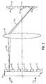
- FIG. 2is a side view of part of a lithographic system used to create a circuit pattern image during lithography.
- FIG. 3is a plan view of a sample circuit pattern to be reproduced on a wafer substrate by photolithography.
- FIG. 4is a plan view of the circuit performance target dimensional bounds of the circuit pattern of FIG. 3 .
- FIG. 5is a plan view of the simulated achievable dimensional bounds of the circuit pattern of FIG. 3 given lithographic process variations.
- FIG. 6is a plan view of the points where the simulated achievable dimensional bounds of FIG. 5 fall outside of the target dimensional bounds of FIG. 4 .
- FIG. 7is a schematic of a computer for running a computer program embodying the method of the present invention.
- FIGS. 1-7 of the drawingsin which like numerals refer to like features of the invention.
- Features of the inventionare not necessarily shown to scale in the drawings.
- the applicantshave determined at least two essential problems with commonly implemented model-based OPC tools.
- the first problemis that the contours of the simulated pattern on which the iterative correction is based are calculated at a single exposure condition, i.e. the modeled image used for OPC represents a snapshot of one possible image which may be obtained for a given process within acceptable values of process fluctuation.
- the modeled image used for OPCrepresents a snapshot of one possible image which may be obtained for a given process within acceptable values of process fluctuation.
- the processis described as a single contour and all information of known and acceptable spread in the actual image edge placement over realistic process windows is lost.
- process windowis used herein to refer to the range of exposure dose and defocus as well as other sources of linewidth variation, such as lens aberrations and mask dimensional errors, over which an acceptable (e.g., 10%) linewidth control can be maintained in lithographic processing of the IC.
- the second problemis that the final measure for the success of the iterative correction is a comparison of the simulated image to the original mask layout. While it is true that, to a first approximation, the task of lithography is to replicate the mask layout, there are well known and acceptable offsets between the layout and the final wafer image, e.g. corner rounding and line end shortening. Furthermore, the specifications put on the circuit design assume a certain amount of fluctuation in the placement of all edges. None of this information can be communicated in model-based OPC tools that optimize against the original layout. Even pre-distorting the original layout cannot capture allowable edge placement tolerances in the optimization.
- the present inventionprovides a new and improved method to implement model-based optical proximity correction based on the principle of improving circuit performance and effective process window.
- the present inventionutilizes otherwise standard OPC to manipulate lithography mask patterns to compensate for a variety of patterning errors in addition to just optical effects.
- FIG. 2An example of a lithography process using a mask made in accordance with the present invention is shown in FIG. 2 .
- Radiation comprising energy beam 30passes through a portion of mask 18 comprising a substrate layer 20 sufficiently transparent to the radiation on which are deposited opaque segments 22 conforming to the circuit pattern image to be projected.
- the beam 30 portion that passes through the mask 18 between opaque segments 22is illustrated by beam 30 a .
- Beam 30 ais focused by lens system 24 onto the surface 32 of a semiconductor wafer having conventional resist materials sensitive to the radiation. Radiation blocked by, mask portions 22 does not transfer to the resist layer on surface 32 .
- a contrasting latent image 28is formed, on wafer resist surface 32 which conforms to the pattern of opaque layer 22 on the mask, except for optical proximity effects.
- the resistis then developed, and the pattern created by the latent image is used to produce a desired circuit or portion thereof on the wafer.
- FIG. 3shows a sample circuit pattern to be reproduced on a wafer substrate by photolithography.
- the first step in the OPC method of the present inventionis to establish target dimensional bounds over which proper circuit performance is guaranteed by the design assumptions and the process error budget.
- the target dimensional boundsestablish how much the particular circuit pattern may vary in size and still provide adequate electrical performance, and may be determined by conventional methods without undue experimentation.
- the target dimensional boundsare around each feature segment and specify the acceptable range of edge displacement for each feature segment.
- FIG. 4shows such target dimensional bounds for the circuit pattern of FIG. 3, and include line width and corner rounding, as well as other, variations.
- Target dimensional boundsmay be derived from design rules of the IC or empirically by experimental data for the circuits on the IC.
- the target dimensional bound of a line segmentis indicated as W 1T
- the target dimensional bound for a line endis indicated as W 2T .
- These target dimensional boundsdepend on intra-feature characteristics, for example, poly over diffusion equals a gate, contact over/under metal equals a critical line end, and the like.
- acceptable variation in metal layer line endmay be determined by location of contacts on adjacent lithographic layers to determine maximum variations before performance is impacted, and other allowable maximum pattern feature variations may be likewise determined for each circuit pattern on each layer.
- the second aspect of the present inventionis the generation of simulated achievable dimensional bounds that outline and establish the spread of the simulated projected image over the required process window, based on assumed process fluctuations and variations.
- the simulated dimensional boundsindicate the edges of the band within which any edge of the input pattern is expected to be imaged over a given range of lithographic process conditions, for example, extremes in dose and focus variation, resist effects, etch variation, as well as other desired modeled process fluctuations.
- the simulated dimensional boundsmay likewise be determined by conventional techniques without undue experimentation. Simulated achievable dimensional bounds may be determined through simulation, by first principle modeling, or through empirical measurements, or some combination thereof (i.e., empirically anchored simulation).
- empirical measurementmay be by measurement of wafer data, or by measurement of the aerial image of the pattern projected by the mask.
- FIG. 5shows the simulated dimensional bounds for the band and feature segments previously identified in FIG. 4 as W 1S and W 2S , respectively.
- Both the target dimensional bounds and the simulated achievable boundsmay be calculated and represented as bands or ranges, as shown in FIGS. 4 and 5, or as maximum-minimum contours, i.e., lines showing only the smallest feature outline and the largest feature outline.
- the present methodcompares the target dimensional bounds of the pattern to the simulated achievable dimensional bounds of the pattern, and determines locations where the simulated achievable dimensional bounds of the pattern exceed the target dimensional bounds of the pattern.
- the target dimensions and locations of line and feature segments W 1T and W 2Twould be respectively compared to the simulated dimensions and locations of line and feature segments W 1S and W 2S (FIG. 5) to determine where the latter exceeds the former in size.
- the method of the present inventionpreferably calculates the total area of the simulated achievable dimensional bounds outside of the acceptable target dimensional bounds, e.g., by adding up the sum of all bad pixels.
- the concept of dimensional bounds as used in the present inventionmay be used to a) characterize a lithographic process by using the bad pixels a metric, b) optimize a process by reducing or eliminating the bad pixels shown in FIG. 6, or c) do OPC.
- the calculation of bad pixelsmay be linked to a program that simulates a variety of process options, e.g., lithographic illumination, mask type resist characteristics, global mask bias, and the like.
- the OPC correction method of the present inventionpreferably involves a two step process. It is important to note that OPC by itself does not improve lithographic process window, i.e., manipulating the mask layout does not significantly reduce the pattern's sensitivity to dose, focus, and other process fluctuations.
- the first task in the present methodis to ensure that the simulated achievable dimensional bounds are always narrower than the target dimensional bounds. That is, independent of the placement of the simulated achievable dimensional bounds, if the spread in edge placement in the simulated image over a given process window is wider than the allowable spread, layout manipulations will fail to converge on a good overlap of the simulated achievable dimensional bound to the target dimensional bound.
- the second preferred step in the present methodis to iteratively manipulate and modify the mask layout data to ensure that all simulated achievable dimensional bounds can be contained within the established target dimensional bounds.
- One way of implementing this optimization iterationis by directly subtracting shapes formed by expanding regions where the simulated achievable dimensional bound falls outside the target dimensional bound from the original mask layout, and adding shapes formed by shrinking regions where the simulated achievable dimensional bound falls inside the target dimensional bound.
- Other optimization techniquesmay be employed.
- the method of the present inventionmay be embodied as a computer program product stored on a program storage device.
- This program storage devicemay be devised, made and used as a component of a machine utilizing optics, magnetic properties and/or electronics to perform the method steps of the present invention.
- Program storage devicesinclude, but are not limited to, magnetic disks or diskettes, magnetic tapes, optical disks, Read Only Memory (ROM), floppy disks, semiconductor chips and the like.
- a computer readable program code means in known source codemay be employed to convert the methods described below for use on a computer.
- the computer program or software incorporating the process steps and instructions described further belowmay be stored in any conventional computer, for example, that shown in FIG. 7 .
- Computer 40incorporates a program storage device 42 and a microprocessor 44 . Installed on the program storage device 42 is the program code incorporating the method of the present invention, as well as any database information for the mask pattern of a feature to be created on the semiconductor substrate and the lithographic process window variations.
Landscapes
- Physics & Mathematics (AREA)
- General Physics & Mathematics (AREA)
- Preparing Plates And Mask In Photomechanical Process (AREA)
- Exposure And Positioning Against Photoresist Photosensitive Materials (AREA)
Abstract
Description
Claims (24)
Priority Applications (1)
| Application Number | Priority Date | Filing Date | Title |
|---|---|---|---|
| US09/759,013US6578190B2 (en) | 2001-01-11 | 2001-01-11 | Process window based optical proximity correction of lithographic images |
Applications Claiming Priority (1)
| Application Number | Priority Date | Filing Date | Title |
|---|---|---|---|
| US09/759,013US6578190B2 (en) | 2001-01-11 | 2001-01-11 | Process window based optical proximity correction of lithographic images |
Publications (2)
| Publication Number | Publication Date |
|---|---|
| US20020091986A1 US20020091986A1 (en) | 2002-07-11 |
| US6578190B2true US6578190B2 (en) | 2003-06-10 |
Family
ID=25054047
Family Applications (1)
| Application Number | Title | Priority Date | Filing Date |
|---|---|---|---|
| US09/759,013Expired - LifetimeUS6578190B2 (en) | 2001-01-11 | 2001-01-11 | Process window based optical proximity correction of lithographic images |
Country Status (1)
| Country | Link |
|---|---|
| US (1) | US6578190B2 (en) |
Cited By (71)
| Publication number | Priority date | Publication date | Assignee | Title |
|---|---|---|---|---|
| US20030219154A1 (en)* | 2002-05-22 | 2003-11-27 | Medvedeva Marina M. | Quality measurement of an aerial image |
| US20040123264A1 (en)* | 2002-12-20 | 2004-06-24 | Numerical Technologies, Inc. | Incremental lithography mask layout design and verification |
| US20050066300A1 (en)* | 2003-09-18 | 2005-03-24 | International Business Machines Corporation | Method for interlayer and yield based optical proximity correction |
| US20050125763A1 (en)* | 2003-06-30 | 2005-06-09 | Taiwan Semiconductor Manufacturing Company, Ltd. | System and method for the online design of a reticle field layout |
| US20050134866A1 (en)* | 2003-12-18 | 2005-06-23 | Suigen Kyoh | Pattern-producing method for semiconductor device |
| US20050160390A1 (en)* | 2004-01-16 | 2005-07-21 | International Business Machines Corporation | Cloned and original circuit shape merging |
| US20050246675A1 (en)* | 2004-05-01 | 2005-11-03 | Scheffer Louis K | Method and apparatus for designing integrated circuit layouts |
| US20050246674A1 (en)* | 2004-05-01 | 2005-11-03 | Scheffer Louis K | Method and apparatus for designing integrated circuit layouts |
| US20060033049A1 (en)* | 2004-08-10 | 2006-02-16 | Toshiya Kotani | Design pattern data preparing method, mask pattern data preparing method, mask manufacturing method, semiconductor device manufacturing method, and program recording medium |
| WO2005109256A3 (en)* | 2004-05-01 | 2006-05-04 | Cadence Design Systems Inc | Methos and apparatus for designing integrated circuit layouts |
| US20060110837A1 (en)* | 2004-11-22 | 2006-05-25 | Blaze Dfm, Inc. | Method and system for topography-aware reticle enhancement |
| US20060110025A1 (en)* | 2004-11-19 | 2006-05-25 | Ho Ming F | Method for inspecting mask defects |
| US20060131271A1 (en)* | 2004-12-22 | 2006-06-22 | Adrian Kiermasz | Methods and apparatus for sequentially alternating among plasma processes in order to optimize a substrate |
| US20060270068A1 (en)* | 2005-05-31 | 2006-11-30 | Taiwan Semiconductor Manufacturing Co., Ltd. | Method for fabricating right-angle holes in a substrate |
| US20070083847A1 (en)* | 2005-10-12 | 2007-04-12 | International Business Machines Corporation | Designer's intent tolerance bands for proximity correction and checking |
| US20070204256A1 (en)* | 2006-02-17 | 2007-08-30 | Mentor Graphics Corporation | Interconnection modeling for semiconductor fabrication process effects |
| US20080052660A1 (en)* | 2006-07-31 | 2008-02-28 | Samsung Electronics Co., Ltd. | Method of correcting a designed pattern of a mask |
| US20080127029A1 (en)* | 2006-10-31 | 2008-05-29 | International Business Machines Corporation | Closed-loop design for manufacturability process |
| US20080141211A1 (en)* | 2006-12-11 | 2008-06-12 | International Business Machines Corporation | Opc verification using auto-windowed regions |
| US20090003684A1 (en)* | 2007-06-29 | 2009-01-01 | Alqudah Yazan A | Defect analysis |
| US20090014811A1 (en)* | 2006-03-09 | 2009-01-15 | Tela Innovations, Inc. | Dynamic Array Architecture |
| US20090032967A1 (en)* | 2007-08-02 | 2009-02-05 | Tela Innovations, Inc. | Semiconductor Device with Dynamic Array Section |
| US20090077525A1 (en)* | 2007-09-14 | 2009-03-19 | Henning Haffner | System and Method for Semiconductor Device Fabrication Using Modeling |
| US20090132992A1 (en)* | 2007-11-21 | 2009-05-21 | Chartered Semiconductor Manufacturing, Ltd. | Statistical optical proximity correction |
| US20090222672A1 (en)* | 2002-04-16 | 2009-09-03 | Massachusetts Institute Of Technology | Integrated Circuit That Uses A Dynamic Characteristic Of The Circuit |
| US20090296055A1 (en)* | 2008-06-03 | 2009-12-03 | Jun Ye | Lens heating compensation systems and methods |
| US20100037200A1 (en)* | 2008-08-11 | 2010-02-11 | Justin Ghan | System and method for model based multi-patterning optimization |
| US7765498B1 (en)* | 2007-05-24 | 2010-07-27 | Xilinx, Inc. | Methods of incorporating process-induced layout dimension changes into an integrated circuit simulation netlist |
| US20100252889A1 (en)* | 2008-03-13 | 2010-10-07 | Tela Innovations, Inc. | Linear Gate Level Cross-Coupled Transistor Device with Contiguous p-type Diffusion Regions and Contiguous n-type Diffusion Regions |
| US20100333049A1 (en)* | 2009-06-26 | 2010-12-30 | International Business Machines Corporation | Model-Based Retargeting of Layout Patterns for Sub-Wavelength Photolithography |
| USRE42294E1 (en)* | 2000-06-30 | 2011-04-12 | Kabushiki Kaisha Toshiba | Semiconductor integrated circuit designing method and system using a design rule modification |
| US7932545B2 (en) | 2006-03-09 | 2011-04-26 | Tela Innovations, Inc. | Semiconductor device and associated layouts including gate electrode level region having arrangement of six linear conductive segments with side-to-side spacing less than 360 nanometers |
| US7941768B1 (en)* | 2006-01-11 | 2011-05-10 | Olambda, Inc. | Photolithographic process simulation in integrated circuit design and manufacturing |
| US7939443B2 (en) | 2008-03-27 | 2011-05-10 | Tela Innovations, Inc. | Methods for multi-wire routing and apparatus implementing same |
| US7943967B2 (en) | 2006-03-09 | 2011-05-17 | Tela Innovations, Inc. | Semiconductor device and associated layouts including diffusion contact placement restriction based on relation to linear conductive segments |
| US20110119642A1 (en)* | 2009-11-17 | 2011-05-19 | International Business Machines Corporation | Simultaneous Photolithographic Mask and Target Optimization |
| US20110138342A1 (en)* | 2009-12-03 | 2011-06-09 | International Business Machines Corporation | Retargeting for Electrical Yield Enhancement |
| US20110167397A1 (en)* | 2008-01-31 | 2011-07-07 | Judy Huckabay | System and method for multi-exposure pattern decomposition |
| US7979829B2 (en) | 2007-02-20 | 2011-07-12 | Tela Innovations, Inc. | Integrated circuit cell library with cell-level process compensation technique (PCT) application and associated methods |
| US7994545B2 (en) | 2007-10-26 | 2011-08-09 | Tela Innovations, Inc. | Methods, structures, and designs for self-aligning local interconnects used in integrated circuits |
| US20110209106A1 (en)* | 2010-02-19 | 2011-08-25 | International Business Machines Corporation | Method for designing optical lithography masks for directed self-assembly |
| US8209656B1 (en) | 2008-10-14 | 2012-06-26 | Cadence Design Systems, Inc. | Pattern decomposition method |
| US8214778B2 (en) | 2007-08-02 | 2012-07-03 | Tela Innovations, Inc. | Methods for cell phasing and placement in dynamic array architecture and implementation of the same |
| US8225261B2 (en) | 2006-03-09 | 2012-07-17 | Tela Innovations, Inc. | Methods for defining contact grid in dynamic array architecture |
| US8225239B2 (en) | 2006-03-09 | 2012-07-17 | Tela Innovations, Inc. | Methods for defining and utilizing sub-resolution features in linear topology |
| CN101349862B (en)* | 2008-08-19 | 2012-08-08 | 上海宏力半导体制造有限公司 | Method for calibrating optical approach correcting model based on multi-photoresist active diffusion length |
| US8245180B2 (en) | 2006-03-09 | 2012-08-14 | Tela Innovations, Inc. | Methods for defining and using co-optimized nanopatterns for integrated circuit design and apparatus implementing same |
| US8247846B2 (en) | 2006-03-09 | 2012-08-21 | Tela Innovations, Inc. | Oversized contacts and vias in semiconductor chip defined by linearly constrained topology |
| US8286107B2 (en) | 2007-02-20 | 2012-10-09 | Tela Innovations, Inc. | Methods and systems for process compensation technique acceleration |
| US8331646B2 (en) | 2009-12-23 | 2012-12-11 | International Business Machines Corporation | Optical proximity correction for transistors using harmonic mean of gate length |
| US8448102B2 (en) | 2006-03-09 | 2013-05-21 | Tela Innovations, Inc. | Optimizing layout of irregular structures in regular layout context |
| US8453094B2 (en) | 2008-01-31 | 2013-05-28 | Tela Innovations, Inc. | Enforcement of semiconductor structure regularity for localized transistors and interconnect |
| US8473874B1 (en) | 2011-08-22 | 2013-06-25 | Cadence Design Systems, Inc. | Method and apparatus for automatically fixing double patterning loop violations |
| US8516402B1 (en) | 2011-08-22 | 2013-08-20 | Cadence Design Systems, Inc. | Method and apparatus for automatically fixing double patterning loop violations |
| US8515715B2 (en) | 2011-06-17 | 2013-08-20 | International Business Machines Corporation | Method, system and program storage device for simulating electronic device performance as a function of process variations |
| US8541879B2 (en) | 2007-12-13 | 2013-09-24 | Tela Innovations, Inc. | Super-self-aligned contacts and method for making the same |
| US8653857B2 (en) | 2006-03-09 | 2014-02-18 | Tela Innovations, Inc. | Circuitry and layouts for XOR and XNOR logic |
| US8661392B2 (en) | 2009-10-13 | 2014-02-25 | Tela Innovations, Inc. | Methods for cell boundary encroachment and layouts implementing the Same |
| US8658542B2 (en) | 2006-03-09 | 2014-02-25 | Tela Innovations, Inc. | Coarse grid design methods and structures |
| US8667443B2 (en) | 2007-03-05 | 2014-03-04 | Tela Innovations, Inc. | Integrated circuit cell library for multiple patterning |
| US8839175B2 (en) | 2006-03-09 | 2014-09-16 | Tela Innovations, Inc. | Scalable meta-data objects |
| US8863063B2 (en) | 2009-05-06 | 2014-10-14 | Tela Innovations, Inc. | Finfet transistor circuit |
| US9035359B2 (en) | 2006-03-09 | 2015-05-19 | Tela Innovations, Inc. | Semiconductor chip including region including linear-shaped conductive structures forming gate electrodes and having electrical connection areas arranged relative to inner region between transistors of different types and associated methods |
| US9122832B2 (en) | 2008-08-01 | 2015-09-01 | Tela Innovations, Inc. | Methods for controlling microloading variation in semiconductor wafer layout and fabrication |
| US9158878B2 (en)* | 2013-08-23 | 2015-10-13 | Kabushiki Kaisha Toshiba | Method and apparatus for generating circuit layout using design model and specification |
| US9159627B2 (en) | 2010-11-12 | 2015-10-13 | Tela Innovations, Inc. | Methods for linewidth modification and apparatus implementing the same |
| US9230910B2 (en) | 2006-03-09 | 2016-01-05 | Tela Innovations, Inc. | Oversized contacts and vias in layout defined by linearly constrained topology |
| US9311442B2 (en)* | 2014-04-25 | 2016-04-12 | Globalfoundries Inc. | Net-voltage-aware optical proximity correction (OPC) |
| US9563733B2 (en) | 2009-05-06 | 2017-02-07 | Tela Innovations, Inc. | Cell circuit and layout with linear finfet structures |
| US10216890B2 (en) | 2004-04-21 | 2019-02-26 | Iym Technologies Llc | Integrated circuits having in-situ constraints |
| US20220035240A1 (en)* | 2020-07-28 | 2022-02-03 | Synopsys, Inc. | Wafer sensitivity determination and communication |
Families Citing this family (14)
| Publication number | Priority date | Publication date | Assignee | Title |
|---|---|---|---|---|
| TWI252516B (en)* | 2002-03-12 | 2006-04-01 | Toshiba Corp | Determination method of process parameter and method for determining at least one of process parameter and design rule |
| US6777147B1 (en) | 2003-05-21 | 2004-08-17 | International Business Machines Corporation | Method for evaluating the effects of multiple exposure processes in lithography |
| US7318214B1 (en) | 2003-06-19 | 2008-01-08 | Invarium, Inc. | System and method for reducing patterning variability in integrated circuit manufacturing through mask layout corrections |
| US7115343B2 (en)* | 2004-03-10 | 2006-10-03 | International Business Machines Corporation | Pliant SRAF for improved performance and manufacturability |
| US7266800B2 (en)* | 2004-06-04 | 2007-09-04 | Invarium, Inc. | Method and system for designing manufacturable patterns that account for the pattern- and position-dependent nature of patterning processes |
| US7588868B2 (en)* | 2004-10-06 | 2009-09-15 | Cadence Design Systems, Inc. | Method and system for reducing the impact of across-wafer variations on critical dimension measurements |
| US7596420B2 (en)* | 2006-06-19 | 2009-09-29 | Asml Netherlands B.V. | Device manufacturing method and computer program product |
| US20080241709A1 (en)* | 2007-04-02 | 2008-10-02 | Kent Nakagawa | System And Method For analyzing photomask Geometries |
| NL1036189A1 (en)* | 2007-12-05 | 2009-06-08 | Brion Tech Inc | Methods and System for Lithography Process Window Simulation. |
| US8775977B2 (en)* | 2011-02-15 | 2014-07-08 | Taiwan Semiconductor Manufacturing Co., Ltd | Decomposition and marking of semiconductor device design layout in double patterning lithography |
| US8631361B2 (en)* | 2012-05-29 | 2014-01-14 | Taiwan Semiconductor Manufacturing Company, Ltd. | Integrated circuit design method with dynamic target point |
| KR102219460B1 (en)* | 2014-09-04 | 2021-02-24 | 삼성전자주식회사 | Method of decomposing layout of semiconductor device and method of manufacturing semiconductor device using the same |
| CN114063380B (en)* | 2020-08-07 | 2025-02-18 | 中芯国际集成电路制造(上海)有限公司 | Pattern correction method and semiconductor structure forming method |
| CN115220297A (en)* | 2022-08-18 | 2022-10-21 | 上海积塔半导体有限公司 | OPC (optical proximity correction) pattern correction method and system and mask plate |
Citations (21)
| Publication number | Priority date | Publication date | Assignee | Title |
|---|---|---|---|---|
| US5340700A (en) | 1992-04-06 | 1994-08-23 | Microunity Systems Engineering, Inc. | Method for improved lithographic patterning in a semiconductor fabrication process |
| US5723235A (en)* | 1993-11-08 | 1998-03-03 | Sony Corporation | Method of producing photomask and exposing |
| US5723233A (en) | 1996-02-27 | 1998-03-03 | Lsi Logic Corporation | Optical proximity correction method and apparatus |
| US5795688A (en)* | 1996-08-14 | 1998-08-18 | Micron Technology, Inc. | Process for detecting defects in photomasks through aerial image comparisons |
| US5801954A (en)* | 1996-04-24 | 1998-09-01 | Micron Technology, Inc. | Process for designing and checking a mask layout |
| US5889686A (en)* | 1996-08-22 | 1999-03-30 | Kabushiki Kaisha Toshiba | Profile simulation method |
| US5965306A (en)* | 1997-10-15 | 1999-10-12 | International Business Machines Corporation | Method of determining the printability of photomask defects |
| US6077310A (en)* | 1995-12-22 | 2000-06-20 | Kabushiki Kaisha Toshiba | Optical proximity correction system |
| US6078738A (en)* | 1997-05-08 | 2000-06-20 | Lsi Logic Corporation | Comparing aerial image to SEM of photoresist or substrate pattern for masking process characterization |
| US6081658A (en) | 1997-12-31 | 2000-06-27 | Avant! Corporation | Proximity correction system for wafer lithography |
| US6178360B1 (en)* | 1998-02-05 | 2001-01-23 | Micron Technology, Inc. | Methods and apparatus for determining optimum exposure threshold for a given photolithographic model |
| US6249597B1 (en)* | 1995-07-17 | 2001-06-19 | Sony Corporation | Method of correcting mask pattern and mask, method of exposure, apparatus thereof, and photomask and semiconductor device using the same |
| US6261728B1 (en)* | 1998-10-19 | 2001-07-17 | Vanguard International Semiconductor Corporation | Mask image scanning exposure method |
| US6272392B1 (en)* | 1998-12-04 | 2001-08-07 | Advanced Micro Devices, Inc. | Methodology for extracting effective lens aberrations using a neural network |
| US6340543B1 (en)* | 1999-10-19 | 2002-01-22 | Mitsubishi Denki Kabushiki Kaisha | Photomask, manufacturing method thereof, and semiconductor device |
| US6345210B1 (en)* | 1999-03-08 | 2002-02-05 | Advanced Micro Devices, Inc. | Method of using critical dimension mapping to qualify a reticle used in integrated circuit fabrication |
| US6388736B1 (en)* | 1999-11-15 | 2002-05-14 | Asm Lithography B.V. | Imaging method using phase boundary masking with modified illumination |
| US6418553B1 (en)* | 1999-03-12 | 2002-07-09 | Kabushiki Kaisha Toshiba | Circuit designing method for semiconductor device and computer-readable medium |
| US20020100004A1 (en)* | 2000-09-29 | 2002-07-25 | Numerical Technologies, Inc. | Selection of evaluation point locations based on proximity effects model amplitudes for correcting proximity effects in a fabrication layout |
| US6470489B1 (en)* | 1997-09-17 | 2002-10-22 | Numerical Technologies, Inc. | Design rule checking system and method |
| US6472107B1 (en)* | 1999-09-30 | 2002-10-29 | Photronics, Inc. | Disposable hard mask for photomask plasma etching |
- 2001
- 2001-01-11USUS09/759,013patent/US6578190B2/ennot_activeExpired - Lifetime
Patent Citations (22)
| Publication number | Priority date | Publication date | Assignee | Title |
|---|---|---|---|---|
| US5340700A (en) | 1992-04-06 | 1994-08-23 | Microunity Systems Engineering, Inc. | Method for improved lithographic patterning in a semiconductor fabrication process |
| US5723235A (en)* | 1993-11-08 | 1998-03-03 | Sony Corporation | Method of producing photomask and exposing |
| US6249597B1 (en)* | 1995-07-17 | 2001-06-19 | Sony Corporation | Method of correcting mask pattern and mask, method of exposure, apparatus thereof, and photomask and semiconductor device using the same |
| US6077310A (en)* | 1995-12-22 | 2000-06-20 | Kabushiki Kaisha Toshiba | Optical proximity correction system |
| US5723233A (en) | 1996-02-27 | 1998-03-03 | Lsi Logic Corporation | Optical proximity correction method and apparatus |
| US5801954A (en)* | 1996-04-24 | 1998-09-01 | Micron Technology, Inc. | Process for designing and checking a mask layout |
| US5795688A (en)* | 1996-08-14 | 1998-08-18 | Micron Technology, Inc. | Process for detecting defects in photomasks through aerial image comparisons |
| US5889686A (en)* | 1996-08-22 | 1999-03-30 | Kabushiki Kaisha Toshiba | Profile simulation method |
| US6078738A (en)* | 1997-05-08 | 2000-06-20 | Lsi Logic Corporation | Comparing aerial image to SEM of photoresist or substrate pattern for masking process characterization |
| US6470489B1 (en)* | 1997-09-17 | 2002-10-22 | Numerical Technologies, Inc. | Design rule checking system and method |
| US5965306A (en)* | 1997-10-15 | 1999-10-12 | International Business Machines Corporation | Method of determining the printability of photomask defects |
| US6081658A (en) | 1997-12-31 | 2000-06-27 | Avant! Corporation | Proximity correction system for wafer lithography |
| US6178360B1 (en)* | 1998-02-05 | 2001-01-23 | Micron Technology, Inc. | Methods and apparatus for determining optimum exposure threshold for a given photolithographic model |
| US6261728B1 (en)* | 1998-10-19 | 2001-07-17 | Vanguard International Semiconductor Corporation | Mask image scanning exposure method |
| US6272392B1 (en)* | 1998-12-04 | 2001-08-07 | Advanced Micro Devices, Inc. | Methodology for extracting effective lens aberrations using a neural network |
| US6345210B1 (en)* | 1999-03-08 | 2002-02-05 | Advanced Micro Devices, Inc. | Method of using critical dimension mapping to qualify a reticle used in integrated circuit fabrication |
| US6418553B1 (en)* | 1999-03-12 | 2002-07-09 | Kabushiki Kaisha Toshiba | Circuit designing method for semiconductor device and computer-readable medium |
| US6472107B1 (en)* | 1999-09-30 | 2002-10-29 | Photronics, Inc. | Disposable hard mask for photomask plasma etching |
| US6340543B1 (en)* | 1999-10-19 | 2002-01-22 | Mitsubishi Denki Kabushiki Kaisha | Photomask, manufacturing method thereof, and semiconductor device |
| US6388736B1 (en)* | 1999-11-15 | 2002-05-14 | Asm Lithography B.V. | Imaging method using phase boundary masking with modified illumination |
| US20020100004A1 (en)* | 2000-09-29 | 2002-07-25 | Numerical Technologies, Inc. | Selection of evaluation point locations based on proximity effects model amplitudes for correcting proximity effects in a fabrication layout |
| US6453457B1 (en)* | 2000-09-29 | 2002-09-17 | Numerical Technologies, Inc. | Selection of evaluation point locations based on proximity effects model amplitudes for correcting proximity effects in a fabrication layout |
Cited By (289)
| Publication number | Priority date | Publication date | Assignee | Title |
|---|---|---|---|---|
| USRE42294E1 (en)* | 2000-06-30 | 2011-04-12 | Kabushiki Kaisha Toshiba | Semiconductor integrated circuit designing method and system using a design rule modification |
| USRE43659E1 (en) | 2000-06-30 | 2012-09-11 | Kabushiki Kaisha Toshiba | Method for making a design layout of a semiconductor integrated circuit |
| US8386801B2 (en) | 2002-04-16 | 2013-02-26 | Massachusetts Institute Of Technology | Authentication of integrated circuits |
| US20090222672A1 (en)* | 2002-04-16 | 2009-09-03 | Massachusetts Institute Of Technology | Integrated Circuit That Uses A Dynamic Characteristic Of The Circuit |
| US7904731B2 (en)* | 2002-04-16 | 2011-03-08 | Massachusetts Institute Of Technology | Integrated circuit that uses a dynamic characteristic of the circuit |
| US20030219154A1 (en)* | 2002-05-22 | 2003-11-27 | Medvedeva Marina M. | Quality measurement of an aerial image |
| US7035446B2 (en)* | 2002-05-22 | 2006-04-25 | Lsi Logic Corporation | Quality measurement of an aerial image |
| US20040123264A1 (en)* | 2002-12-20 | 2004-06-24 | Numerical Technologies, Inc. | Incremental lithography mask layout design and verification |
| US6904587B2 (en)* | 2002-12-20 | 2005-06-07 | Synopsys, Inc. | Incremental lithography mask layout design and verification |
| US20050125763A1 (en)* | 2003-06-30 | 2005-06-09 | Taiwan Semiconductor Manufacturing Company, Ltd. | System and method for the online design of a reticle field layout |
| US20060031809A1 (en)* | 2003-09-18 | 2006-02-09 | Zach Franz X | Method for interlayer and yield based optical proximity correction |
| US20080086715A1 (en)* | 2003-09-18 | 2008-04-10 | Zach Franz X | Method for interlayer and yield based optical proximity correction |
| US7861209B2 (en) | 2003-09-18 | 2010-12-28 | International Business Machines Corporation | Method for interlayer and yield based optical proximity correction |
| US7712069B2 (en) | 2003-09-18 | 2010-05-04 | International Business Machines Corporation | Method for interlayer and yield based optical proximity correction |
| US6961920B2 (en) | 2003-09-18 | 2005-11-01 | International Business Machines Corporation | Method for interlayer and yield based optical proximity correction |
| US20080022255A1 (en)* | 2003-09-18 | 2008-01-24 | Zach Franz X | Method for interlayer and yield based optical proximity correction |
| US7334212B2 (en) | 2003-09-18 | 2008-02-19 | International Business Machines Corporation | Method for interlayer and yield based optical proximity correction |
| US20050066300A1 (en)* | 2003-09-18 | 2005-03-24 | International Business Machines Corporation | Method for interlayer and yield based optical proximity correction |
| US7966584B2 (en) | 2003-12-18 | 2011-06-21 | Kabushiki Kaisha Toshiba | Pattern-producing method for semiconductor device |
| US7523437B2 (en)* | 2003-12-18 | 2009-04-21 | Kabushiki Kaisha Toshiba | Pattern-producing method for semiconductor device |
| US20050134866A1 (en)* | 2003-12-18 | 2005-06-23 | Suigen Kyoh | Pattern-producing method for semiconductor device |
| US20050160390A1 (en)* | 2004-01-16 | 2005-07-21 | International Business Machines Corporation | Cloned and original circuit shape merging |
| US7120887B2 (en)* | 2004-01-16 | 2006-10-10 | International Business Machines Corporation | Cloned and original circuit shape merging |
| US10846454B2 (en) | 2004-04-21 | 2020-11-24 | Iym Technologies Llc | Integrated circuits having in-situ constraints |
| US10216890B2 (en) | 2004-04-21 | 2019-02-26 | Iym Technologies Llc | Integrated circuits having in-situ constraints |
| US10860773B2 (en) | 2004-04-21 | 2020-12-08 | Iym Technologies Llc | Integrated circuits having in-situ constraints |
| WO2005109256A3 (en)* | 2004-05-01 | 2006-05-04 | Cadence Design Systems Inc | Methos and apparatus for designing integrated circuit layouts |
| US7082588B2 (en)* | 2004-05-01 | 2006-07-25 | Cadence Design Systems, Inc. | Method and apparatus for designing integrated circuit layouts |
| US20050246675A1 (en)* | 2004-05-01 | 2005-11-03 | Scheffer Louis K | Method and apparatus for designing integrated circuit layouts |
| US20050246674A1 (en)* | 2004-05-01 | 2005-11-03 | Scheffer Louis K | Method and apparatus for designing integrated circuit layouts |
| US7254798B2 (en) | 2004-05-01 | 2007-08-07 | Cadence Design Systems, Inc | Method and apparatus for designing integrated circuit layouts |
| US20060033049A1 (en)* | 2004-08-10 | 2006-02-16 | Toshiya Kotani | Design pattern data preparing method, mask pattern data preparing method, mask manufacturing method, semiconductor device manufacturing method, and program recording medium |
| US7526748B2 (en)* | 2004-08-10 | 2009-04-28 | Kabushiki Kaisha Toshiba | Design pattern data preparing method, mask pattern data preparing method, mask manufacturing method, semiconductor device manufacturing method, and program recording medium |
| US20060110025A1 (en)* | 2004-11-19 | 2006-05-25 | Ho Ming F | Method for inspecting mask defects |
| US7814456B2 (en) | 2004-11-22 | 2010-10-12 | Tela Innovations, Inc. | Method and system for topography-aware reticle enhancement |
| US20060110837A1 (en)* | 2004-11-22 | 2006-05-25 | Blaze Dfm, Inc. | Method and system for topography-aware reticle enhancement |
| US7459100B2 (en)* | 2004-12-22 | 2008-12-02 | Lam Research Corporation | Methods and apparatus for sequentially alternating among plasma processes in order to optimize a substrate |
| US20060131271A1 (en)* | 2004-12-22 | 2006-06-22 | Adrian Kiermasz | Methods and apparatus for sequentially alternating among plasma processes in order to optimize a substrate |
| WO2006068971A3 (en)* | 2004-12-22 | 2007-09-20 | Lam Res Corp | Sequentially alternating plasma process parameters to optimize a substrate |
| CN101287860B (en)* | 2004-12-22 | 2011-10-05 | 朗姆研究公司 | Method and apparatus for sequential alternation in a plasma process to optimize a substrate |
| US20060270068A1 (en)* | 2005-05-31 | 2006-11-30 | Taiwan Semiconductor Manufacturing Co., Ltd. | Method for fabricating right-angle holes in a substrate |
| US7381654B2 (en) | 2005-05-31 | 2008-06-03 | Taiwan Semiconductor Manufacturing Co. | Method for fabricating right-angle holes in a substrate |
| US20070261013A1 (en)* | 2005-10-12 | 2007-11-08 | International Business Machines Corporation | Designer's intent tolerance bands for proximity correction and checking |
| US7607114B2 (en) | 2005-10-12 | 2009-10-20 | International Business Machines Corporation | Designer's intent tolerance bands for proximity correction and checking |
| US7266798B2 (en) | 2005-10-12 | 2007-09-04 | International Business Machines Corporation | Designer's intent tolerance bands for proximity correction and checking |
| US20070083847A1 (en)* | 2005-10-12 | 2007-04-12 | International Business Machines Corporation | Designer's intent tolerance bands for proximity correction and checking |
| US7941768B1 (en)* | 2006-01-11 | 2011-05-10 | Olambda, Inc. | Photolithographic process simulation in integrated circuit design and manufacturing |
| US20090276749A1 (en)* | 2006-02-17 | 2009-11-05 | Mentor Graphics Corporation | Gate modeling for semiconductor fabrication process effects |
| US8015510B2 (en)* | 2006-02-17 | 2011-09-06 | Mentor Graphics Corporation | Interconnection modeling for semiconductor fabrication process effects |
| US8813017B2 (en) | 2006-02-17 | 2014-08-19 | Mentor Graphics Corporation | Gate modeling for semiconductor fabrication process effects |
| US8051393B2 (en) | 2006-02-17 | 2011-11-01 | Mentor Graphics Corporation | Gate modeling for semiconductor fabrication process effects |
| US20070204256A1 (en)* | 2006-02-17 | 2007-08-30 | Mentor Graphics Corporation | Interconnection modeling for semiconductor fabrication process effects |
| US8258552B2 (en) | 2006-03-09 | 2012-09-04 | Tela Innovations, Inc. | Semiconductor device including at least six transistor forming linear shapes with at least two transistor forming linear shapes having offset ends |
| US9917056B2 (en) | 2006-03-09 | 2018-03-13 | Tela Innovations, Inc. | Coarse grid design methods and structures |
| US8823062B2 (en) | 2006-03-09 | 2014-09-02 | Tela Innovations, Inc. | Integrated circuit with offset line end spacings in linear gate electrode level |
| US20100096671A1 (en)* | 2006-03-09 | 2010-04-22 | Tela Innovations, Inc. | Cell of Semiconductor Device Having Gate Electrode Conductive Structures Formed from Rectangular Shaped Gate Electrode Layout Features and At Least Eight Transistors |
| US7842975B2 (en) | 2006-03-09 | 2010-11-30 | Tela Innovations, Inc. | Dynamic array architecture |
| US8839175B2 (en) | 2006-03-09 | 2014-09-16 | Tela Innovations, Inc. | Scalable meta-data objects |
| US8658542B2 (en) | 2006-03-09 | 2014-02-25 | Tela Innovations, Inc. | Coarse grid design methods and structures |
| US8921896B2 (en) | 2006-03-09 | 2014-12-30 | Tela Innovations, Inc. | Integrated circuit including linear gate electrode structures having different extension distances beyond contact |
| US8653857B2 (en) | 2006-03-09 | 2014-02-18 | Tela Innovations, Inc. | Circuitry and layouts for XOR and XNOR logic |
| US8921897B2 (en) | 2006-03-09 | 2014-12-30 | Tela Innovations, Inc. | Integrated circuit with gate electrode conductive structures having offset ends |
| US7906801B2 (en) | 2006-03-09 | 2011-03-15 | Tela Innovations, Inc. | Semiconductor device and associated layouts having transistors formed from six linear conductive segments with intervening diffusion contact restrictions |
| US7910958B2 (en) | 2006-03-09 | 2011-03-22 | Tela Innovations, Inc. | Semiconductor device and associated layouts having transistors formed from linear conductive segment with non-active neighboring linear conductive segment |
| US7910959B2 (en) | 2006-03-09 | 2011-03-22 | Tela Innovations, Inc. | Semiconductor device and associated layouts having transistors formed from six linear conductive segments with gate electrode connection through single interconnect level |
| US8946781B2 (en) | 2006-03-09 | 2015-02-03 | Tela Innovations, Inc. | Integrated circuit including gate electrode conductive structures with different extension distances beyond contact |
| US7923757B2 (en) | 2006-03-09 | 2011-04-12 | Tela Innovations, Inc. | Semiconductor device and associated layouts having linear shaped gate electrodes defined along at least five adjacent gate electrode tracks of equal pitch with gate electrode connection through single interconnect level |
| US20100011331A1 (en)* | 2006-03-09 | 2010-01-14 | Tela Innovations, Inc. | Semiconductor Device Layout Including Cell Layout Having Restricted Gate Electrode Level Layout with Linear Shaped Gate Electrode Layout Features Defined Along At Least Four Gate Electrode Tracks with Minimum End-to-End Spacing with Corresponding Non-Symmetric Diffusion Regions |
| US7932545B2 (en) | 2006-03-09 | 2011-04-26 | Tela Innovations, Inc. | Semiconductor device and associated layouts including gate electrode level region having arrangement of six linear conductive segments with side-to-side spacing less than 360 nanometers |
| US7932544B2 (en) | 2006-03-09 | 2011-04-26 | Tela Innovations, Inc. | Semiconductor device and associated layouts including linear conductive segments having non-gate extension portions |
| US20100006902A1 (en)* | 2006-03-09 | 2010-01-14 | Tela Innovations, Inc. | Semiconductor Device Portion Having Sub-Wavelength-Sized Gate Electrode Conductive Structures Formed from Rectangular Shaped Gate Electrode Layout Features Defined Along At Least Four Gate Electrode Tracks and Having Corresponding Non-Symmetric Diffusion Regions |
| US8952425B2 (en) | 2006-03-09 | 2015-02-10 | Tela Innovations, Inc. | Integrated circuit including at least four linear-shaped conductive structures having extending portions of different length |
| US7943966B2 (en) | 2006-03-09 | 2011-05-17 | Tela Innovations, Inc. | Integrated circuit and associated layout with gate electrode level portion including at least two complimentary transistor forming linear conductive segments and at least one non-gate linear conductive segment |
| US7943967B2 (en) | 2006-03-09 | 2011-05-17 | Tela Innovations, Inc. | Semiconductor device and associated layouts including diffusion contact placement restriction based on relation to linear conductive segments |
| US10230377B2 (en) | 2006-03-09 | 2019-03-12 | Tela Innovations, Inc. | Circuitry and layouts for XOR and XNOR logic |
| US7948012B2 (en) | 2006-03-09 | 2011-05-24 | Tela Innovations, Inc. | Semiconductor device having 1965 nm gate electrode level region including at least four active linear conductive segments and at least one non-gate linear conductive segment |
| US7948013B2 (en) | 2006-03-09 | 2011-05-24 | Tela Innovations, Inc. | Semiconductor device and associated layouts having linear shaped gate electrodes defined along at least five adjacent gate electrode tracks of equal pitch |
| US7952119B2 (en) | 2006-03-09 | 2011-05-31 | Tela Innovations, Inc. | Semiconductor device and associated layout having three or more linear-shaped gate electrode level conductive segments of both equal length and equal pitch |
| US10217763B2 (en) | 2006-03-09 | 2019-02-26 | Tela Innovations, Inc. | Semiconductor chip having region including gate electrode features of rectangular shape on gate horizontal grid and first-metal structures of rectangular shape on at least eight first-metal gridlines of first-metal vertical grid |
| US9009641B2 (en) | 2006-03-09 | 2015-04-14 | Tela Innovations, Inc. | Circuits with linear finfet structures |
| US10186523B2 (en) | 2006-03-09 | 2019-01-22 | Tela Innovations, Inc. | Semiconductor chip having region including gate electrode features formed in part from rectangular layout shapes on gate horizontal grid and first-metal structures formed in part from rectangular layout shapes on at least eight first-metal gridlines of first-metal vertical grid |
| US9035359B2 (en) | 2006-03-09 | 2015-05-19 | Tela Innovations, Inc. | Semiconductor chip including region including linear-shaped conductive structures forming gate electrodes and having electrical connection areas arranged relative to inner region between transistors of different types and associated methods |
| US9230910B2 (en) | 2006-03-09 | 2016-01-05 | Tela Innovations, Inc. | Oversized contacts and vias in layout defined by linearly constrained topology |
| US7989848B2 (en) | 2006-03-09 | 2011-08-02 | Tela Innovations, Inc. | Semiconductor device having at least four side-by-side electrodes of equal length and equal pitch with at least two transistor connections to power or ground |
| US7989847B2 (en) | 2006-03-09 | 2011-08-02 | Tela Innovations, Inc. | Semiconductor device having linear-shaped gate electrodes of different transistor types with uniformity extending portions of different lengths |
| US9240413B2 (en) | 2006-03-09 | 2016-01-19 | Tela Innovations, Inc. | Methods, structures, and designs for self-aligning local interconnects used in integrated circuits |
| US10141335B2 (en) | 2006-03-09 | 2018-11-27 | Tela Innovations, Inc. | Semiconductor CIP including region having rectangular-shaped gate structures and first metal structures |
| US9336344B2 (en) | 2006-03-09 | 2016-05-10 | Tela Innovations, Inc. | Coarse grid design methods and structures |
| US8022441B2 (en) | 2006-03-09 | 2011-09-20 | Tela Innovations, Inc. | Semiconductor device and associated layouts having transistors formed from six linear conductive segments with gate electrode-to-gate electrode connection through single interconnect level and common node connection through different interconnect level |
| US8030689B2 (en) | 2006-03-09 | 2011-10-04 | Tela Innovations, Inc. | Integrated circuit device and associated layout including separated diffusion regions of different type each having four gate electrodes with each of two complementary gate electrode pairs formed from respective linear conductive segment |
| US9425272B2 (en) | 2006-03-09 | 2016-08-23 | Tela Innovations, Inc. | Semiconductor chip including integrated circuit including four transistors of first transistor type and four transistors of second transistor type with electrical connections between various transistors and methods for manufacturing the same |
| US8035133B2 (en) | 2006-03-09 | 2011-10-11 | Tela Innovations, Inc. | Semiconductor device having two pairs of transistors of different types formed from shared linear-shaped conductive features with intervening transistors of common type on equal pitch |
| US9425273B2 (en) | 2006-03-09 | 2016-08-23 | Tela Innovations, Inc. | Semiconductor chip including integrated circuit including at least five gate level conductive structures having particular spatial and electrical relationship and method for manufacturing the same |
| US8058671B2 (en) | 2006-03-09 | 2011-11-15 | Tela Innovations, Inc. | Semiconductor device having at least three linear-shaped electrode level conductive features of equal length positioned side-by-side at equal pitch |
| US10141334B2 (en) | 2006-03-09 | 2018-11-27 | Tela Innovations, Inc. | Semiconductor chip including region having rectangular-shaped gate structures and first-metal structures |
| US9425145B2 (en) | 2006-03-09 | 2016-08-23 | Tela Innovations, Inc. | Oversized contacts and vias in layout defined by linearly constrained topology |
| US8448102B2 (en) | 2006-03-09 | 2013-05-21 | Tela Innovations, Inc. | Optimizing layout of irregular structures in regular layout context |
| US8072003B2 (en) | 2006-03-09 | 2011-12-06 | Tela Innovations, Inc. | Integrated circuit device and associated layout including two pairs of co-aligned complementary gate electrodes with offset gate contact structures |
| US8089103B2 (en) | 2006-03-09 | 2012-01-03 | Tela Innovations, Inc. | Integrated circuit device with gate level region including at least three linear-shaped conductive segments having offset line ends and forming three transistors of first type and one transistor of second type |
| US8089098B2 (en) | 2006-03-09 | 2012-01-03 | Tela Innovations, Inc. | Integrated circuit device and associated layout including linear gate electrodes of different transistor types next to linear-shaped non-gate conductive segment |
| US8089104B2 (en) | 2006-03-09 | 2012-01-03 | Tela Innovations, Inc. | Integrated circuit with gate electrode level region including multiple linear-shaped conductive structures forming gate electrodes of transistors and including uniformity extending portions of different size |
| US8089099B2 (en) | 2006-03-09 | 2012-01-03 | Tela Innovations, Inc, | Integrated circuit device and associated layout including gate electrode level region of 965 NM radius with linear-shaped conductive segments on fixed pitch |
| US8089100B2 (en) | 2006-03-09 | 2012-01-03 | Tela Innovations, Inc. | Integrated circuit with gate electrode level region including at least four linear-shaped conductive structures forming gate electrodes of transistors and including extending portions of at least two different sizes |
| US8088681B2 (en) | 2006-03-09 | 2012-01-03 | Tela Innovations, Inc. | Method for fabricating integrated circuit including separated diffusion regions of different type each having four gate electrodes with each of two complementary gate electrode pairs formed from respective linear condcutive segment |
| US8089101B2 (en) | 2006-03-09 | 2012-01-03 | Tela Innovations, Inc. | Integrated circuit device with gate electrode level region including two side-by-side ones of at least three linear-shaped conductive structures electrically connected to each other through non-gate level |
| US8088682B2 (en) | 2006-03-09 | 2012-01-03 | Tela Innovations, Inc. | Method for fabricating integrated circuit with gate electrode level region including two side-by-side ones of at least three linear-shaped conductive structures electrically connected to each other through non-gate level |
| US8088680B2 (en) | 2006-03-09 | 2012-01-03 | Tela Innovations, Inc. | Method for fabricating integrated circuit having at least three linear-shaped gate electrode level conductive features of equal length positioned side-by-side at equal pitch |
| US8089102B2 (en) | 2006-03-09 | 2012-01-03 | Tela Innovations, Inc. | Method for fabricating integrated circuit having three or more linear-shaped gate electrode level conductive segments of both equal length and equal pitch |
| US8088679B2 (en) | 2006-03-09 | 2012-01-03 | Tela Innovations, Inc. | Method for fabricating integrated circuit with gate electrode level portion including at least two complementary transistor forming linear conductive segments and at least one non-gate linear conductive segment |
| US8101975B2 (en) | 2006-03-09 | 2012-01-24 | Tela Innovations, Inc. | Integrated circuit device with gate level region including non-gate linear conductive segment positioned within 965 nanometers of four transistors of first type and four transistors of second type |
| US8110854B2 (en) | 2006-03-09 | 2012-02-07 | Tela Innovations, Inc. | Integrated circuit device with linearly defined gate electrode level region and shared diffusion region of first type connected to shared diffusion region of second type through at least two interconnect levels |
| US8129751B2 (en) | 2006-03-09 | 2012-03-06 | Tela Innovations, Inc. | Integrated circuit including at least six linear-shaped conductive structures forming gate electrodes and including four conductive contacting structures having at least two different connection distances |
| US8129757B2 (en) | 2006-03-09 | 2012-03-06 | Tela Innovations, Inc. | Integrated circuit including at least six linear-shaped conductive structive structures at equal pitch including at least two linear-shaped conductive structures having non-gate portions of different length |
| US8129756B2 (en) | 2006-03-09 | 2012-03-06 | Tela Innovations, Inc. | Integrated circuit including at least six linear-shaped conductive structures forming gate electrodes of transistors with at least two different extension distances beyond conductive contacting structures |
| US8129753B2 (en) | 2006-03-09 | 2012-03-06 | Tela Innovations, Inc. | Integrated circuit including gate electrode level region including at least seven linear-shaped conductive structures of equal length positioned at equal pitch with at least two linear-shaped conductive structures each forming one transistor and having extending portion sized greater than gate portion |
| US8129750B2 (en) | 2006-03-09 | 2012-03-06 | Tela Innovations, Inc. | Integrated circuit including at least six linear-shaped conductive structures forming gate electrodes of transistors with at least two linear-shaped conductive structures of different length |
| US8129755B2 (en) | 2006-03-09 | 2012-03-06 | Tela Innovations, Inc. | Integrated circuit with gate electrode level including at least four linear-shaped conductive structures of equal length and equal pitch with linear-shaped conductive structure forming one transistor |
| US8129754B2 (en) | 2006-03-09 | 2012-03-06 | Tela Innovations, Inc. | Integrated circuit with gate electrode level including at least six linear-shaped conductive structures forming gate electrodes of transisters with at least one pair of linear-shaped conductive structures having offset ends |
| US8129819B2 (en) | 2006-03-09 | 2012-03-06 | Tela Innovations, Inc. | Method of fabricating integrated circuit including at least six linear-shaped conductive structures at equal pitch including at least two linear-shaped conductive structures having non-gate portions of different length |
| US8129752B2 (en) | 2006-03-09 | 2012-03-06 | Tela Innovations, Inc. | Integrated circuit including a linear-shaped conductive structure forming one gate electrode and having length greater than or equal to one-half the length of linear-shaped conductive structure forming two gate electrodes |
| US8134183B2 (en) | 2006-03-09 | 2012-03-13 | Tela Innovations, Inc. | Integrated circuit including linear-shaped conductive structures that have gate portions and extending portions of different size |
| US8134184B2 (en) | 2006-03-09 | 2012-03-13 | Tela Innovations, Inc. | Integrated circuit having gate electrode level region including at least four linear-shaped conductive structures with some outer-contacted linear-shaped conductive structures having larger outer extending portion than inner extending portion |
| US8134186B2 (en) | 2006-03-09 | 2012-03-13 | Tela Innovations, Inc. | Integrated circuit including at least three linear-shaped conductive structures at equal pitch including linear-shaped conductive structure having non-gate portion length greater than gate portion length |
| US8134185B2 (en) | 2006-03-09 | 2012-03-13 | Tela Innovations, Inc. | Integrated circuit having gate electrode level region including at least seven linear-shaped conductive structures at equal pitch including linear-shaped conductive structure forming transistors of two different types and at least three linear-shaped conductive structures having aligned ends |
| US8138525B2 (en) | 2006-03-09 | 2012-03-20 | Tela Innovations, Inc. | Integrated circuit including at least three linear-shaped conductive structures of different length each forming gate of different transistor |
| US8436400B2 (en) | 2006-03-09 | 2013-05-07 | Tela Innovations, Inc. | Semiconductor device with gate level including gate electrode conductors for transistors of first type and transistors of second type with some gate electrode conductors of different length |
| US9443947B2 (en) | 2006-03-09 | 2016-09-13 | Tela Innovations, Inc. | Semiconductor chip including region having integrated circuit transistor gate electrodes formed by various conductive structures of specified shape and position and method for manufacturing the same |
| US8198656B2 (en) | 2006-03-09 | 2012-06-12 | Tela Innovations, Inc. | Integrated circuit including gate electrode level region including at least four linear-shaped conductive structures of equal length having aligned ends and positioned at equal pitch and forming multiple gate electrodes of transistors of different type |
| US9589091B2 (en) | 2006-03-09 | 2017-03-07 | Tela Innovations, Inc. | Scalable meta-data objects |
| US8207053B2 (en) | 2006-03-09 | 2012-06-26 | Tela Innovations, Inc. | Electrodes of transistors with at least two linear-shaped conductive structures of different length |
| US20090014811A1 (en)* | 2006-03-09 | 2009-01-15 | Tela Innovations, Inc. | Dynamic Array Architecture |
| US8217428B2 (en) | 2006-03-09 | 2012-07-10 | Tela Innovations, Inc. | Integrated circuit including gate electrode level region including at least three linear-shaped conductive structures of equal length having aligned ends and positioned at equal pitch and forming multiple gate electrodes of transistors of different type |
| US8225261B2 (en) | 2006-03-09 | 2012-07-17 | Tela Innovations, Inc. | Methods for defining contact grid in dynamic array architecture |
| US8225239B2 (en) | 2006-03-09 | 2012-07-17 | Tela Innovations, Inc. | Methods for defining and utilizing sub-resolution features in linear topology |
| US9905576B2 (en) | 2006-03-09 | 2018-02-27 | Tela Innovations, Inc. | Semiconductor chip including region having rectangular-shaped gate structures and first metal structures |
| US9859277B2 (en) | 2006-03-09 | 2018-01-02 | Tela Innovations, Inc. | Methods, structures, and designs for self-aligning local interconnects used in integrated circuits |
| US8245180B2 (en) | 2006-03-09 | 2012-08-14 | Tela Innovations, Inc. | Methods for defining and using co-optimized nanopatterns for integrated circuit design and apparatus implementing same |
| US8247846B2 (en) | 2006-03-09 | 2012-08-21 | Tela Innovations, Inc. | Oversized contacts and vias in semiconductor chip defined by linearly constrained topology |
| US8253173B2 (en) | 2006-03-09 | 2012-08-28 | Tela Innovations, Inc. | Semiconductor device with gate level including four transistors of first type and four transistors of second type separated by non-diffusion region and having at least two gate contacts positioned outside separating non-diffusion region |
| US8253172B2 (en) | 2006-03-09 | 2012-08-28 | Tela Innovations, Inc. | Semiconductor device with linearly restricted gate level region including four serially connected transistors of first type and four serially connected transistors of second type separated by non-diffusion region |
| US8258547B2 (en) | 2006-03-09 | 2012-09-04 | Tela Innovations, Inc. | Semiconductor device with linearly restricted gate level region including two transistors of first type and two transistors of second type with offset gate contacts |
| US9673825B2 (en) | 2006-03-09 | 2017-06-06 | Tela Innovations, Inc. | Circuitry and layouts for XOR and XNOR logic |
| US8258551B2 (en) | 2006-03-09 | 2012-09-04 | Tela Innovations, Inc. | Semiconductor device with gate level including transistors of first type and transistors of second type with corresponding gate contact placement restriction |
| US8258549B2 (en) | 2006-03-09 | 2012-09-04 | Tela Innovations, Inc. | Semiconductor device including two transistors of first type having gates formed by conductors of different length respectively aligned with two transistors of second type having gates formed by conductors of different length |
| US9711495B2 (en) | 2006-03-09 | 2017-07-18 | Tela Innovations, Inc. | Oversized contacts and vias in layout defined by linearly constrained topology |
| US8258548B2 (en) | 2006-03-09 | 2012-09-04 | Tela Innovations, Inc. | Semiconductor device with gate level including four transistors of first type and four transistors of second type separated by non-diffusion region with restricted gate contact placement over separating non-diffusion region |
| US8258550B2 (en) | 2006-03-09 | 2012-09-04 | Tela Innovations, Inc. | Semiconductor device including at least six transistor forming linear shapes including at least two transistor forming linear shapes having different extension distances beyond gate contact |
| US8264009B2 (en) | 2006-03-09 | 2012-09-11 | Tela Innovations, Inc. | Semiconductor device with linearly restricted gate level region including four transistors of first type and four transistors of second type with gate defining shapes of different length |
| US9741719B2 (en) | 2006-03-09 | 2017-08-22 | Tela Innovations, Inc. | Methods, structures, and designs for self-aligning local interconnects used in integrated circuits |
| US8264008B2 (en) | 2006-03-09 | 2012-09-11 | Tela Innovations, Inc. | Semiconductor device including transistor forming linear shapes including gate portions and extending portions of different size |
| US8264007B2 (en) | 2006-03-09 | 2012-09-11 | Tela Innovations, Inc. | Semiconductor device including at least six transistor forming linear shapes including at least two different gate contact connection distances |
| US9754878B2 (en) | 2006-03-09 | 2017-09-05 | Tela Innovations, Inc. | Semiconductor chip including a chip level based on a layout that includes both regular and irregular wires |
| US20080052660A1 (en)* | 2006-07-31 | 2008-02-28 | Samsung Electronics Co., Ltd. | Method of correcting a designed pattern of a mask |
| US7624369B2 (en) | 2006-10-31 | 2009-11-24 | International Business Machines Corporation | Closed-loop design for manufacturability process |
| US20080127029A1 (en)* | 2006-10-31 | 2008-05-29 | International Business Machines Corporation | Closed-loop design for manufacturability process |
| US20080141211A1 (en)* | 2006-12-11 | 2008-06-12 | International Business Machines Corporation | Opc verification using auto-windowed regions |
| US7562337B2 (en)* | 2006-12-11 | 2009-07-14 | International Business Machines Corporation | OPC verification using auto-windowed regions |
| US8286107B2 (en) | 2007-02-20 | 2012-10-09 | Tela Innovations, Inc. | Methods and systems for process compensation technique acceleration |
| US7979829B2 (en) | 2007-02-20 | 2011-07-12 | Tela Innovations, Inc. | Integrated circuit cell library with cell-level process compensation technique (PCT) application and associated methods |
| US8667443B2 (en) | 2007-03-05 | 2014-03-04 | Tela Innovations, Inc. | Integrated circuit cell library for multiple patterning |
| US9633987B2 (en) | 2007-03-05 | 2017-04-25 | Tela Innovations, Inc. | Integrated circuit cell library for multiple patterning |
| US10074640B2 (en) | 2007-03-05 | 2018-09-11 | Tela Innovations, Inc. | Integrated circuit cell library for multiple patterning |
| US8966424B2 (en) | 2007-03-07 | 2015-02-24 | Tela Innovations, Inc. | Methods for cell phasing and placement in dynamic array architecture and implementation of the same |
| US9424387B2 (en) | 2007-03-07 | 2016-08-23 | Tela Innovations, Inc. | Methods for cell phasing and placement in dynamic array architecture and implementation of the same |
| US9910950B2 (en) | 2007-03-07 | 2018-03-06 | Tela Innovations, Inc. | Methods for cell phasing and placement in dynamic array architecture and implementation of the same |
| US9595515B2 (en) | 2007-03-07 | 2017-03-14 | Tela Innovations, Inc. | Semiconductor chip including integrated circuit defined within dynamic array section |
| US7765498B1 (en)* | 2007-05-24 | 2010-07-27 | Xilinx, Inc. | Methods of incorporating process-induced layout dimension changes into an integrated circuit simulation netlist |
| US20090003684A1 (en)* | 2007-06-29 | 2009-01-01 | Alqudah Yazan A | Defect analysis |
| US8064682B2 (en)* | 2007-06-29 | 2011-11-22 | Intel Corporation | Defect analysis |
| US7917879B2 (en) | 2007-08-02 | 2011-03-29 | Tela Innovations, Inc. | Semiconductor device with dynamic array section |
| US8214778B2 (en) | 2007-08-02 | 2012-07-03 | Tela Innovations, Inc. | Methods for cell phasing and placement in dynamic array architecture and implementation of the same |
| US8759882B2 (en) | 2007-08-02 | 2014-06-24 | Tela Innovations, Inc. | Semiconductor device with dynamic array sections defined and placed according to manufacturing assurance halos |
| US8283701B2 (en) | 2007-08-02 | 2012-10-09 | Tela Innovations, Inc. | Semiconductor device with dynamic array sections defined and placed according to manufacturing assurance halos |
| US8356268B2 (en) | 2007-08-02 | 2013-01-15 | Tela Innovations, Inc. | Integrated circuit device including dynamic array section with gate level having linear conductive features on at least three side-by-side lines and uniform line end spacings |
| US8549455B2 (en) | 2007-08-02 | 2013-10-01 | Tela Innovations, Inc. | Methods for cell phasing and placement in dynamic array architecture and implementation of the same |
| US7888705B2 (en) | 2007-08-02 | 2011-02-15 | Tela Innovations, Inc. | Methods for defining dynamic array section with manufacturing assurance halo and apparatus implementing the same |
| US8756551B2 (en) | 2007-08-02 | 2014-06-17 | Tela Innovations, Inc. | Methods for designing semiconductor device with dynamic array section |
| US7908578B2 (en) | 2007-08-02 | 2011-03-15 | Tela Innovations, Inc. | Methods for designing semiconductor device with dynamic array section |
| US20090032967A1 (en)* | 2007-08-02 | 2009-02-05 | Tela Innovations, Inc. | Semiconductor Device with Dynamic Array Section |
| US7669176B2 (en) | 2007-09-14 | 2010-02-23 | Infineon Technologies Ag | System and method for semiconductor device fabrication using modeling |
| US20090077525A1 (en)* | 2007-09-14 | 2009-03-19 | Henning Haffner | System and Method for Semiconductor Device Fabrication Using Modeling |
| US10734383B2 (en) | 2007-10-26 | 2020-08-04 | Tela Innovations, Inc. | Methods, structures, and designs for self-aligning local interconnects used in integrated circuits |
| US8680626B2 (en) | 2007-10-26 | 2014-03-25 | Tela Innovations, Inc. | Methods, structures, and designs for self-aligning local interconnects used in integrated circuits |
| US7994545B2 (en) | 2007-10-26 | 2011-08-09 | Tela Innovations, Inc. | Methods, structures, and designs for self-aligning local interconnects used in integrated circuits |
| US20090132992A1 (en)* | 2007-11-21 | 2009-05-21 | Chartered Semiconductor Manufacturing, Ltd. | Statistical optical proximity correction |
| US8572524B2 (en) | 2007-11-21 | 2013-10-29 | Globalfoundries Singapore Pte. Ltd. | Statistical optical proximity correction |
| US9281371B2 (en) | 2007-12-13 | 2016-03-08 | Tela Innovations, Inc. | Super-self-aligned contacts and method for making the same |
| US8951916B2 (en) | 2007-12-13 | 2015-02-10 | Tela Innovations, Inc. | Super-self-aligned contacts and method for making the same |
| US10461081B2 (en) | 2007-12-13 | 2019-10-29 | Tel Innovations, Inc. | Super-self-aligned contacts and method for making the same |
| US8541879B2 (en) | 2007-12-13 | 2013-09-24 | Tela Innovations, Inc. | Super-self-aligned contacts and method for making the same |
| US9818747B2 (en) | 2007-12-13 | 2017-11-14 | Tela Innovations, Inc. | Super-self-aligned contacts and method for making the same |
| US8151219B2 (en) | 2008-01-31 | 2012-04-03 | Cadence Design Systems, Inc. | System and method for multi-exposure pattern decomposition |
| US9530734B2 (en) | 2008-01-31 | 2016-12-27 | Tela Innovations, Inc. | Enforcement of semiconductor structure regularity for localized transistors and interconnect |
| US9202779B2 (en) | 2008-01-31 | 2015-12-01 | Tela Innovations, Inc. | Enforcement of semiconductor structure regularity for localized transistors and interconnect |
| US20110167397A1 (en)* | 2008-01-31 | 2011-07-07 | Judy Huckabay | System and method for multi-exposure pattern decomposition |
| US8701071B2 (en) | 2008-01-31 | 2014-04-15 | Tela Innovations, Inc. | Enforcement of semiconductor structure regularity for localized transistors and interconnect |
| US8453094B2 (en) | 2008-01-31 | 2013-05-28 | Tela Innovations, Inc. | Enforcement of semiconductor structure regularity for localized transistors and interconnect |
| US9081931B2 (en) | 2008-03-13 | 2015-07-14 | Tela Innovations, Inc. | Cross-coupled transistor circuit having diffusion regions of common node on opposing sides of same gate electrode track and gate node connection through single interconnect layer |
| US8258581B2 (en) | 2008-03-13 | 2012-09-04 | Tela Innovations, Inc. | Integrated circuit including cross-coupled transistors with two transistors of different type formed by same gate level structure and two transistors of different type formed by separate gate level structures |
| US8735944B2 (en) | 2008-03-13 | 2014-05-27 | Tela Innovations, Inc. | Integrated circuit including cross-coupled transistors having gate electrodes formed within gate level feature layout channels with serially connected transistors |
| US8742463B2 (en) | 2008-03-13 | 2014-06-03 | Tela Innovations, Inc. | Integrated circuit including cross-coupled transistors having gate electrodes formed within gate level feature layout channels with outer positioned gate contacts |
| US8742462B2 (en) | 2008-03-13 | 2014-06-03 | Tela Innovations, Inc. | Integrated circuit including cross-coupled transistors having gate electrodes formed within gate level feature layout channels with gate contact position specifications |
| US8729643B2 (en) | 2008-03-13 | 2014-05-20 | Tela Innovations, Inc. | Cross-coupled transistor circuit including offset inner gate contacts |
| US20100252889A1 (en)* | 2008-03-13 | 2010-10-07 | Tela Innovations, Inc. | Linear Gate Level Cross-Coupled Transistor Device with Contiguous p-type Diffusion Regions and Contiguous n-type Diffusion Regions |
| US8729606B2 (en) | 2008-03-13 | 2014-05-20 | Tela Innovations, Inc. | Integrated circuit including cross-coupled transistors having gate electrodes formed within gate level feature layout channels |
| US8772839B2 (en) | 2008-03-13 | 2014-07-08 | Tela Innovations, Inc. | Integrated circuit including cross-coupled transistors having gate electrodes formed within gate level feature layout channels with four inside positioned gate contacts having offset and aligned relationships and electrical connection of transistor gates through linear interconnect conductors in single interconnect layer |
| US8785979B2 (en) | 2008-03-13 | 2014-07-22 | Tela Innovations, Inc. | Integrated circuit including cross-coupled transistors having gate electrodes formed within gate level feature layout channels with two inside positioned gate contacts and two outside positioned gate contacts and electrical connection of cross-coupled transistors through same interconnect layer |
| US8785978B2 (en) | 2008-03-13 | 2014-07-22 | Tela Innovations, Inc. | Integrated circuit including cross-coupled transistors having gate electrodes formed within gate level feature layout channels with electrical connection of cross-coupled transistors through same interconnect layer |
| US8680583B2 (en) | 2008-03-13 | 2014-03-25 | Tela Innovations, Inc. | Integrated circuit including cross-coupled transistors having gate electrodes formed within at least nine gate level feature layout channels |
| US8816402B2 (en) | 2008-03-13 | 2014-08-26 | Tela Innovations, Inc. | Integrated circuit including cross-coupled transistors having gate electrodes formed within gate level feature layout channels with gate level feature layout channel including single transistor |
| US8669595B2 (en) | 2008-03-13 | 2014-03-11 | Tela Innovations, Inc. | Integrated circuit including cross-coupled transistors having gate electrodes formed within gate level feature layout channels with gate contact position, alignment, and offset specifications |
| US8669594B2 (en) | 2008-03-13 | 2014-03-11 | Tela Innovations, Inc. | Integrated circuit including cross-coupled transistors having gate electrodes formed within at least twelve gate level feature layout channels |
| US8835989B2 (en) | 2008-03-13 | 2014-09-16 | Tela Innovations, Inc. | Integrated circuit including cross-coupled transistors having gate electrodes formed within gate level feature layout channels with gate electrode placement specifications |
| US8836045B2 (en) | 2008-03-13 | 2014-09-16 | Tela Innovations, Inc. | Cross-coupled transistor circuit having diffusion regions of common node on opposing sides of same gate electrode track |
| US8847329B2 (en) | 2008-03-13 | 2014-09-30 | Tela Innovations, Inc. | Cross-coupled transistor circuit defined having diffusion regions of common node on opposing sides of same gate electrode track with at least two non-inner positioned gate contacts |
| US8847331B2 (en) | 2008-03-13 | 2014-09-30 | Tela Innovations, Inc. | Semiconductor chip including region having cross-coupled transistor configuration with offset electrical connection areas on gate electrode forming conductive structures and at least two different inner extension distances of gate electrode forming conductive structures |
| US8853793B2 (en) | 2008-03-13 | 2014-10-07 | Tela Innovations, Inc. | Integrated circuit including gate electrode level region including cross-coupled transistors having gate contacts located over inner portion of gate electrode level region and offset gate level feature line ends |
| US8853794B2 (en) | 2008-03-13 | 2014-10-07 | Tela Innovations, Inc. | Integrated circuit within semiconductor chip including cross-coupled transistor configuration |
| US10727252B2 (en) | 2008-03-13 | 2020-07-28 | Tela Innovations, Inc. | Semiconductor chip including integrated circuit having cross-coupled transistor configuration and method for manufacturing the same |
| US10658385B2 (en) | 2008-03-13 | 2020-05-19 | Tela Innovations, Inc. | Cross-coupled transistor circuit defined on four gate electrode tracks |
| US8866197B2 (en) | 2008-03-13 | 2014-10-21 | Tela Innovations, Inc. | Integrated circuit including cross-coupled transistors having gate electrodes formed within gate level feature layout channels with at least two gate electrodes electrically connected to each other through another transistor forming gate level feature |
| US8872283B2 (en) | 2008-03-13 | 2014-10-28 | Tela Innovations, Inc. | Integrated circuit including cross-coupled transistors having gate electrodes formed within gate level feature layout channels with shared diffusion regions on opposite sides of two-transistor-forming gate level feature |
| US10651200B2 (en) | 2008-03-13 | 2020-05-12 | Tela Innovations, Inc. | Cross-coupled transistor circuit defined on three gate electrode tracks |
| US8592872B2 (en) | 2008-03-13 | 2013-11-26 | Tela Innovations, Inc. | Integrated circuit including cross-coupled transistors with two transistors of different type having gate electrodes formed by common gate level feature with shared diffusion regions on opposite sides of common gate level feature |
| US8587034B2 (en) | 2008-03-13 | 2013-11-19 | Tela Innovations, Inc. | Integrated circuit including cross-coupled transistors having gate electrodes formed within gate level feature layout channels with four inside positioned gate contacts and electrical connection of transistor gates through linear interconnect conductors in single interconnect layer |
| US8581304B2 (en) | 2008-03-13 | 2013-11-12 | Tela Innovations, Inc. | Integrated circuit including cross-coupled transistors having gate electrodes formed within gate level feature layout channels with four inside positioned gate contacts having offset and aligned relationships |
| US8581303B2 (en) | 2008-03-13 | 2013-11-12 | Tela Innovations, Inc. | Integrated circuit including cross-coupled trasistors having gate electrodes formed within gate level feature layout channels with four inside positioned gate contacts having offset relationships and electrical connection of cross-coupled transistors through same interconnect layer |
| US8575706B2 (en) | 2008-03-13 | 2013-11-05 | Tela Innovations, Inc. | Integrated circuit including cross-coupled transistors having gate electrodes formed within gate level feature layout channels with at least two different gate level features inner extensions beyond gate electrode |
| US7956421B2 (en) | 2008-03-13 | 2011-06-07 | Tela Innovations, Inc. | Cross-coupled transistor layouts in restricted gate level layout architecture |
| US8569841B2 (en) | 2008-03-13 | 2013-10-29 | Tela Innovations, Inc. | Integrated circuit including cross-coupled transistors having gate electrodes formed within gate level feature layout channels with at least one gate level feature extending into adjacent gate level feature layout channel |
| US8564071B2 (en) | 2008-03-13 | 2013-10-22 | Tela Innovations, Inc. | Integrated circuit including cross-coupled transistors having gate electrodes formed within gate level feature layout channels with at least two different gate level feature extensions beyond contact |
| US9117050B2 (en) | 2008-03-13 | 2015-08-25 | Tela Innovations, Inc. | Integrated circuit including cross-coupled transistors having gate electrodes formed within gate level feature layout channels with gate contact position and offset specifications |
| US8058691B2 (en) | 2008-03-13 | 2011-11-15 | Tela Innovations, Inc. | Semiconductor device including cross-coupled transistors formed from linear-shaped gate level features |
| US10020321B2 (en) | 2008-03-13 | 2018-07-10 | Tela Innovations, Inc. | Cross-coupled transistor circuit defined on two gate electrode tracks |
| US9871056B2 (en) | 2008-03-13 | 2018-01-16 | Tela Innovations, Inc. | Semiconductor chip including integrated circuit having cross-coupled transistor configuration and method for manufacturing the same |
| US8558322B2 (en) | 2008-03-13 | 2013-10-15 | Tela Innovations, Inc. | Integrated circuit including cross-coupled transistors having gate electrodes formed within gate level feature layout channels with at least two gate electrodes electrically connected to each other through gate level feature |
| US9208279B2 (en) | 2008-03-13 | 2015-12-08 | Tela Innovations, Inc. | Semiconductor chip including digital logic circuit including linear-shaped conductive structures having electrical connection areas located within inner region between transistors of different type and associated methods |
| US9213792B2 (en) | 2008-03-13 | 2015-12-15 | Tela Innovations, Inc. | Semiconductor chip including digital logic circuit including at least six transistors with some transistors forming cross-coupled transistor configuration and associated methods |
| US8552508B2 (en) | 2008-03-13 | 2013-10-08 | Tela Innovations, Inc. | Integrated circuit including cross-coupled transistors having gate electrodes formed within gate level feature layout channels with shared diffusion regions on opposite sides of two-transistor-forming gate level feature and electrical connection of transistor gates through linear interconnect conductors in single interconnect layer |
| US8552509B2 (en) | 2008-03-13 | 2013-10-08 | Tela Innovations, Inc. | Integrated circuit including cross-coupled transistors having gate electrodes formed within gate level feature layout channels with other transistors positioned between cross-coupled transistors |
| US9245081B2 (en) | 2008-03-13 | 2016-01-26 | Tela Innovations, Inc. | Semiconductor chip including digital logic circuit including at least nine linear-shaped conductive structures collectively forming gate electrodes of at least six transistors with some transistors forming cross-coupled transistor configuration and associated methods |
| US8735995B2 (en) | 2008-03-13 | 2014-05-27 | Tela Innovations, Inc. | Cross-coupled transistor circuit defined on three gate electrode tracks with diffusion regions of common node on opposing sides of same gate electrode track |
| US8264044B2 (en) | 2008-03-13 | 2012-09-11 | Tela Innovations, Inc. | Integrated circuit including cross-coupled transistors having two complementary pairs of co-aligned gate electrodes with offset contacting structures positioned between transistors of different type |
| US8264049B2 (en) | 2008-03-13 | 2012-09-11 | Tela Innovations, Inc. | Integrated circuit including cross-coupled transistors with two transistors of different type having gate electrodes formed by common gate level feature with shared diffusion regions on opposite sides of common gate level feature |
| US8274099B2 (en) | 2008-03-13 | 2012-09-25 | Tela Innovations, Inc. | Integrated circuit including cross-coupled transistors having gate electrodes formed within gate level feature layout channels with gate contact position and offset specifications |
| US8395224B2 (en) | 2008-03-13 | 2013-03-12 | Tela Innovations, Inc. | Linear gate level cross-coupled transistor device with non-overlapping PMOS transistors and non-overlapping NMOS transistors relative to directions of gate electrodes |
| US9536899B2 (en) | 2008-03-13 | 2017-01-03 | Tela Innovations, Inc. | Semiconductor chip including integrated circuit having cross-coupled transistor configuration and method for manufacturing the same |
| US8405163B2 (en) | 2008-03-13 | 2013-03-26 | Tela Innovations, Inc. | Integrated circuit including cross-coupled transistors having gate electrodes formed within gate level feature layout channels with shared diffusion regions on opposite sides of two-transistor-forming gate level feature |
| US8405162B2 (en) | 2008-03-13 | 2013-03-26 | Tela Innovations, Inc. | Integrated circuit including gate electrode level region including cross-coupled transistors having at least one gate contact located over outer portion of gate electrode level region |
| US8471391B2 (en) | 2008-03-27 | 2013-06-25 | Tela Innovations, Inc. | Methods for multi-wire routing and apparatus implementing same |
| US8759985B2 (en) | 2008-03-27 | 2014-06-24 | Tela Innovations, Inc. | Methods for multi-wire routing and apparatus implementing same |
| US7939443B2 (en) | 2008-03-27 | 2011-05-10 | Tela Innovations, Inc. | Methods for multi-wire routing and apparatus implementing same |
| US9779200B2 (en) | 2008-03-27 | 2017-10-03 | Tela Innovations, Inc. | Methods for multi-wire routing and apparatus implementing same |
| US9390215B2 (en) | 2008-03-27 | 2016-07-12 | Tela Innovations, Inc. | Methods for multi-wire routing and apparatus implementing same |
| US20090296055A1 (en)* | 2008-06-03 | 2009-12-03 | Jun Ye | Lens heating compensation systems and methods |
| US9746784B2 (en) | 2008-06-03 | 2017-08-29 | Asml Netherlands B.V. | Lens heating compensation systems and methods |
| US8570485B2 (en)* | 2008-06-03 | 2013-10-29 | Asml Netherlands B.V. | Lens heating compensation systems and methods |
| US9122832B2 (en) | 2008-08-01 | 2015-09-01 | Tela Innovations, Inc. | Methods for controlling microloading variation in semiconductor wafer layout and fabrication |
| US8423928B2 (en) | 2008-08-11 | 2013-04-16 | Cadence Design Systems, Inc. | System and method for model based multi-patterning optimization |
| US8069423B2 (en) | 2008-08-11 | 2011-11-29 | Cadence Design Systems, Inc. | System and method for model based multi-patterning optimization |
| US20100037200A1 (en)* | 2008-08-11 | 2010-02-11 | Justin Ghan | System and method for model based multi-patterning optimization |
| CN101349862B (en)* | 2008-08-19 | 2012-08-08 | 上海宏力半导体制造有限公司 | Method for calibrating optical approach correcting model based on multi-photoresist active diffusion length |
| US8209656B1 (en) | 2008-10-14 | 2012-06-26 | Cadence Design Systems, Inc. | Pattern decomposition method |
| US10446536B2 (en) | 2009-05-06 | 2019-10-15 | Tela Innovations, Inc. | Cell circuit and layout with linear finfet structures |
| US8863063B2 (en) | 2009-05-06 | 2014-10-14 | Tela Innovations, Inc. | Finfet transistor circuit |
| US9563733B2 (en) | 2009-05-06 | 2017-02-07 | Tela Innovations, Inc. | Cell circuit and layout with linear finfet structures |
| US8321818B2 (en) | 2009-06-26 | 2012-11-27 | International Business Machines Corporation | Model-based retargeting of layout patterns for sub-wavelength photolithography |
| US20100333049A1 (en)* | 2009-06-26 | 2010-12-30 | International Business Machines Corporation | Model-Based Retargeting of Layout Patterns for Sub-Wavelength Photolithography |
| US9269702B2 (en) | 2009-10-13 | 2016-02-23 | Tela Innovations, Inc. | Methods for cell boundary encroachment and layouts implementing the same |
| US9530795B2 (en) | 2009-10-13 | 2016-12-27 | Tela Innovations, Inc. | Methods for cell boundary encroachment and semiconductor devices implementing the same |
| US8661392B2 (en) | 2009-10-13 | 2014-02-25 | Tela Innovations, Inc. | Methods for cell boundary encroachment and layouts implementing the Same |
| US8146026B2 (en) | 2009-11-17 | 2012-03-27 | International Business Machines Corporation | Simultaneous photolithographic mask and target optimization |
| US20110119642A1 (en)* | 2009-11-17 | 2011-05-19 | International Business Machines Corporation | Simultaneous Photolithographic Mask and Target Optimization |
| US8495530B2 (en) | 2009-12-03 | 2013-07-23 | International Business Machines Corporation | Retargeting for electrical yield enhancement |
| US8230372B2 (en)* | 2009-12-03 | 2012-07-24 | International Business Machines Corporation | Retargeting for electrical yield enhancement |
| US20110138342A1 (en)* | 2009-12-03 | 2011-06-09 | International Business Machines Corporation | Retargeting for Electrical Yield Enhancement |
| US8331646B2 (en) | 2009-12-23 | 2012-12-11 | International Business Machines Corporation | Optical proximity correction for transistors using harmonic mean of gate length |
| US8336003B2 (en) | 2010-02-19 | 2012-12-18 | International Business Machines Corporation | Method for designing optical lithography masks for directed self-assembly |
| US20110209106A1 (en)* | 2010-02-19 | 2011-08-25 | International Business Machines Corporation | Method for designing optical lithography masks for directed self-assembly |
| US8856693B2 (en) | 2010-02-19 | 2014-10-07 | International Business Machines Corporation | Method for designing optical lithography masks for directed self-assembly |
| US9704845B2 (en) | 2010-11-12 | 2017-07-11 | Tela Innovations, Inc. | Methods for linewidth modification and apparatus implementing the same |
| US9159627B2 (en) | 2010-11-12 | 2015-10-13 | Tela Innovations, Inc. | Methods for linewidth modification and apparatus implementing the same |
| US8515715B2 (en) | 2011-06-17 | 2013-08-20 | International Business Machines Corporation | Method, system and program storage device for simulating electronic device performance as a function of process variations |
| US8516402B1 (en) | 2011-08-22 | 2013-08-20 | Cadence Design Systems, Inc. | Method and apparatus for automatically fixing double patterning loop violations |
| US8473874B1 (en) | 2011-08-22 | 2013-06-25 | Cadence Design Systems, Inc. | Method and apparatus for automatically fixing double patterning loop violations |
| US9158878B2 (en)* | 2013-08-23 | 2015-10-13 | Kabushiki Kaisha Toshiba | Method and apparatus for generating circuit layout using design model and specification |
| US9311442B2 (en)* | 2014-04-25 | 2016-04-12 | Globalfoundries Inc. | Net-voltage-aware optical proximity correction (OPC) |
| US20220035240A1 (en)* | 2020-07-28 | 2022-02-03 | Synopsys, Inc. | Wafer sensitivity determination and communication |
| US11657207B2 (en)* | 2020-07-28 | 2023-05-23 | Synopsys, Inc. | Wafer sensitivity determination and communication |
Also Published As
| Publication number | Publication date |
|---|---|
| US20020091986A1 (en) | 2002-07-11 |
Similar Documents
| Publication | Publication Date | Title |
|---|---|---|
| US6578190B2 (en) | Process window based optical proximity correction of lithographic images | |
| US7712069B2 (en) | Method for interlayer and yield based optical proximity correction | |
| US7624369B2 (en) | Closed-loop design for manufacturability process | |
| US7010775B2 (en) | Method for creating mask pattern for circuit fabrication and method for verifying mask pattern for circuit fabrication | |
| US8161423B1 (en) | Defect filtering optical verification process | |
| US6470489B1 (en) | Design rule checking system and method | |
| US10223494B2 (en) | Semiconductor device manufacturing method and mask manufacturing method | |
| US7194704B2 (en) | Design layout preparing method | |
| TWI742184B (en) | Target optimization method | |
| US8166424B2 (en) | Method for constructing OPC model | |
| US7266801B2 (en) | Design pattern correction method and mask pattern producing method | |
| US6792592B2 (en) | Considering mask writer properties during the optical proximity correction process | |
| US20010029403A1 (en) | Method and apparatus for determining optimum exposure threshold for a given photolithographic model | |
| CN109828433B (en) | Method of correcting mask layout and method of manufacturing semiconductor device using the same | |
| WO1999014638A1 (en) | Design rule checking system and method | |
| US7117475B2 (en) | Method and system for utilizing an isofocal contour to perform optical and process corrections | |
| US6571383B1 (en) | Semiconductor device fabrication using a photomask designed using modeling and empirical testing | |
| US20090281778A1 (en) | Method and system for identifying weak points in an integrated circuit design | |
| US7039896B2 (en) | Gradient method of mask edge correction | |
| TWI385546B (en) | Method and program product for optimizing a design to be formed on a substrate | |
| US20250147411A1 (en) | Method for optimizing photomask | |
| CN120386135A (en) | Mask correction method | |
| Newmark | Optical proximity correction for resolution enhancement technology |
Legal Events
| Date | Code | Title | Description |
|---|---|---|---|
| AS | Assignment | Owner name:INTERNATIONAL BUSINESS MACHINES CORPORATION, NEW Y Free format text:ASSIGNMENT OF ASSIGNORS INTEREST;ASSIGNORS:FERGUSON, RICHARD A.;LAVIN, MARK A.;LIEBMANN, LARS W.;AND OTHERS;REEL/FRAME:012346/0866;SIGNING DATES FROM 20001207 TO 20001212 | |
| AS | Assignment | Owner name:INTERNATIONAL BUSINESS MACHINES CORPORATION, NEW Y Free format text:INVALID ASSIGNMENT.;ASSIGNORS:FERGUSON, RICHARD A.;LAVIN, MARK A.;LIEBMANN, LARS W.;AND OTHERS;REEL/FRAME:011494/0173;SIGNING DATES FROM 20001207 TO 20001212 | |
| FEPP | Fee payment procedure | Free format text:PAYOR NUMBER ASSIGNED (ORIGINAL EVENT CODE: ASPN); ENTITY STATUS OF PATENT OWNER: LARGE ENTITY | |
| STCF | Information on status: patent grant | Free format text:PATENTED CASE | |
| FPAY | Fee payment | Year of fee payment:4 | |
| FPAY | Fee payment | Year of fee payment:8 | |
| REMI | Maintenance fee reminder mailed | ||
| FPAY | Fee payment | Year of fee payment:12 | |
| SULP | Surcharge for late payment | Year of fee payment:11 | |
| AS | Assignment | Owner name:GLOBALFOUNDRIES U.S. 2 LLC, NEW YORK Free format text:ASSIGNMENT OF ASSIGNORS INTEREST;ASSIGNOR:INTERNATIONAL BUSINESS MACHINES CORPORATION;REEL/FRAME:036550/0001 Effective date:20150629 | |
| AS | Assignment | Owner name:GLOBALFOUNDRIES INC., CAYMAN ISLANDS Free format text:ASSIGNMENT OF ASSIGNORS INTEREST;ASSIGNORS:GLOBALFOUNDRIES U.S. 2 LLC;GLOBALFOUNDRIES U.S. INC.;REEL/FRAME:036779/0001 Effective date:20150910 | |
| AS | Assignment | Owner name:WILMINGTON TRUST, NATIONAL ASSOCIATION, DELAWARE Free format text:SECURITY AGREEMENT;ASSIGNOR:GLOBALFOUNDRIES INC.;REEL/FRAME:049490/0001 Effective date:20181127 | |
| AS | Assignment | Owner name:GLOBALFOUNDRIES U.S. INC., CALIFORNIA Free format text:ASSIGNMENT OF ASSIGNORS INTEREST;ASSIGNOR:GLOBALFOUNDRIES INC.;REEL/FRAME:054633/0001 Effective date:20201022 | |
| AS | Assignment | Owner name:GLOBALFOUNDRIES INC., CAYMAN ISLANDS Free format text:RELEASE BY SECURED PARTY;ASSIGNOR:WILMINGTON TRUST, NATIONAL ASSOCIATION;REEL/FRAME:054636/0001 Effective date:20201117 | |
| AS | Assignment | Owner name:GLOBALFOUNDRIES U.S. INC., NEW YORK Free format text:RELEASE BY SECURED PARTY;ASSIGNOR:WILMINGTON TRUST, NATIONAL ASSOCIATION;REEL/FRAME:056987/0001 Effective date:20201117 |