US6577476B1 - Flux guide structure for a spin valve transistor which includes a slider body semiconductor layer - Google Patents
Flux guide structure for a spin valve transistor which includes a slider body semiconductor layerDownload PDFInfo
- Publication number
- US6577476B1 US6577476B1US10/108,688US10868802AUS6577476B1US 6577476 B1US6577476 B1US 6577476B1US 10868802 AUS10868802 AUS 10868802AUS 6577476 B1US6577476 B1US 6577476B1
- Authority
- US
- United States
- Prior art keywords
- layer
- svt
- free layer
- semiconductor material
- slider
- Prior art date
- Legal status (The legal status is an assumption and is not a legal conclusion. Google has not performed a legal analysis and makes no representation as to the accuracy of the status listed.)
- Expired - Lifetime
Links
Images


Classifications
- G—PHYSICS
- G11—INFORMATION STORAGE
- G11B—INFORMATION STORAGE BASED ON RELATIVE MOVEMENT BETWEEN RECORD CARRIER AND TRANSDUCER
- G11B5/00—Recording by magnetisation or demagnetisation of a record carrier; Reproducing by magnetic means; Record carriers therefor
- G11B5/127—Structure or manufacture of heads, e.g. inductive
- G11B5/33—Structure or manufacture of flux-sensitive heads, i.e. for reproduction only; Combination of such heads with means for recording or erasing only
- G11B5/332—Structure or manufacture of flux-sensitive heads, i.e. for reproduction only; Combination of such heads with means for recording or erasing only using thin films
- B—PERFORMING OPERATIONS; TRANSPORTING
- B82—NANOTECHNOLOGY
- B82Y—SPECIFIC USES OR APPLICATIONS OF NANOSTRUCTURES; MEASUREMENT OR ANALYSIS OF NANOSTRUCTURES; MANUFACTURE OR TREATMENT OF NANOSTRUCTURES
- B82Y10/00—Nanotechnology for information processing, storage or transmission, e.g. quantum computing or single electron logic
- G—PHYSICS
- G01—MEASURING; TESTING
- G01R—MEASURING ELECTRIC VARIABLES; MEASURING MAGNETIC VARIABLES
- G01R33/00—Arrangements or instruments for measuring magnetic variables
- G01R33/02—Measuring direction or magnitude of magnetic fields or magnetic flux
- G01R33/06—Measuring direction or magnitude of magnetic fields or magnetic flux using galvano-magnetic devices
- G—PHYSICS
- G11—INFORMATION STORAGE
- G11B—INFORMATION STORAGE BASED ON RELATIVE MOVEMENT BETWEEN RECORD CARRIER AND TRANSDUCER
- G11B5/00—Recording by magnetisation or demagnetisation of a record carrier; Reproducing by magnetic means; Record carriers therefor
- G11B5/012—Recording on, or reproducing or erasing from, magnetic disks
- G—PHYSICS
- G11—INFORMATION STORAGE
- G11B—INFORMATION STORAGE BASED ON RELATIVE MOVEMENT BETWEEN RECORD CARRIER AND TRANSDUCER
- G11B5/00—Recording by magnetisation or demagnetisation of a record carrier; Reproducing by magnetic means; Record carriers therefor
- G11B5/127—Structure or manufacture of heads, e.g. inductive
- G11B5/31—Structure or manufacture of heads, e.g. inductive using thin films
- G11B5/3103—Structure or manufacture of integrated heads or heads mechanically assembled and electrically connected to a support or housing
- G11B5/3106—Structure or manufacture of integrated heads or heads mechanically assembled and electrically connected to a support or housing where the integrated or assembled structure comprises means for conditioning against physical detrimental influence, e.g. wear, contamination
Definitions
- a spin-valve transistoris a hybrid device in which ferromagnetic and semiconductor materials have been functionally integrated.
- the SVTis based on spin-dependent transport but, unlike other magnetoresistive devices, it relies on the spin-transport of a portion of transmitted electrons which are energetic “hot” electrons.
- a conventional SVThas three terminals which include a base, emitter, and collector.
- the collectoris made from semiconductor materials (such as silicon) but the other materials are magnetic and contain an anti-ferromagnet.
- an energy barrieror “Schottky” barrier
- thin layers of platinum and goldfor example, are incorporated at the emitter and collector side, respectively. These layers also separate the magnetic layers from the direct contact with silicon.
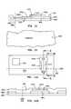
- FIG. 4is an isometric illustration of an exemplary suspension system for supporting the slider and magnetic head
- FIG. 14Bis a cross-sectional view of that shown in FIG. 14A where an additional via to the substrate lies along the plane IX—IX of FIG. 14A;
- FIG. 18is a cross-sectional view of that shown in FIG. 16A except that a lead layer is formed over the top of recessed sensor portion and insulator;
- FIG. 24is another flowchart which provides an alternative method of making the SVT.
- Magnetic head 40may be employed for writing information to multiple circular tracks on the surface of disk 34 , as well as for reading information therefrom.
- Processing circuitry 50exchanges signals representing such information with magnetic head 40 , provides motor drive signals, and also provides control signals for moving slider 42 to various tracks.
- slider 42is shown mounted to a head gimbal assembly (HGA) 52 that is mounted to suspension 44 . All of the above components are supported on a base 53 .
- HGAhead gimbal assembly
- FIG. 5is a side cross-sectional elevation view of a merged read/write head 40 which has a write head portion 54 and a read head portion 56 . Note also the partial ABS view of head 40 in FIG. 7 .
- Read head portionincludes a giant magnetoresistive read (GMR) sensor 58 .
- GMR sensor 58is sandwiched between first and second gap layers 60 and 62 that are, in turn, sandwiched between first and second shield layers 64 and 66 .
- the resistance of GMR sensor 58changes.
- a sense current conducted through the sensorcauses these resistance changes to be manifested as potential changes, which are processed by processing circuitry 50 (FIG. 3 ).
- Write head portion 54 of the headincludes a coil layer 68 sandwiched between first and second insulation layers 70 and 72 .
- a third insulation layer 74may be employed for planarizing the head to eliminate ripples in the second insulation layer caused by coil layer 68 .
- the first, second and third insulation layersare referred to as an “insulation stack”.
- Coil layer 68 , and first, second and third insulation layers 70 , 72 and 74are sandwiched between first and second pole piece layers 76 and 78 .
- the first and second pole piece layers 76 and 78are magnetically coupled at a back gap 80 , and have first and second pole tips 82 and 84 that are separated by a non-magnetic gap layer 86 at the ABS. As shown in FIGS.
- SVTspin valve transistor
- an air bearing surface (ABS) line 910is contemplated for fabrication of the SVT and read head.
- the ABSis the media interface between the sensor and the media (e.g., disk) which stores the data.
- holesare patterned and formed through silicon dioxide layer 806 (FIG. 8) such that surface portions 902 and 903 of semiconductor material 804 are exposed and a silicon-dioxide portion 904 remains. This patterning and forming is done by photolithography and etching. The holes provide “vias” to semiconductor material 804 , which forms the collector of the SVT.
- the frontmost hole relative to contemplated ABS line 910is formed generally at the position shown in FIG.
- FIG. 10shows a top plan view of this resulting structure, where the vias to the substrate may or may not be in alignment Sensor layer formation is now described.
- a thin interfacial energy barriersuch as a Schottky barrier using a metal, e.g. CoFe, NiFe, Pt, or Au
- a free layer 1102is then deposited over the exposed surface portions 902 of semiconductor material 804 (or the Schottky barrier 811 ) as well as silicon dioxide portions 904 . Physical contact is made between free layer 1102 and semiconductor material 804 at its interface.
- free layer 1102extends far enough to the left of the diagram to at least meet, and preferably extend through, contemplated ABS line 910 .
- free layer 1102is formed of a soft magnetic material, such as nickel-iron (NiFe) or cobalt-iron (CoFe), which has a thickness between about 10-60 Angstroms.
- free layer 1102is or includes a ferromagnet (FM).
- FMferromagnet
- the depositing of free layer 1102 , barrier layer 1104 , and magnetic pinned layer 1302is performed by vacuum deposition (e.g. ion beam deposition, sputtering, or evaporation) and may all be deposited in-situ. Note that, similar to free layer 1102 , barrier layer 1202 and magnetic pinned layer 1302 at least meet and preferably extend through contemplated ABS line 910 .
- FIG. 13shows a top plan view of this structure after free layer 1102 , barrier layer 1202 , and magnetic pinned layer 1302 have been deposited across the entire wafer.
- a cross-section of the wafermay resemble that shown in FIG. 12 and FIG. 14 B. This shows that portions of sensor stack 1313 may or may not be in contact with substrate 804 .
- Refilled oxide layer 1311may have semiconductor material 804 or silicon dioxide portion 904 beneath it Note that the thickness of oxide layer 1311 is similar to the thickness of sensor stack 1313 .
- FIG. 14AA top-down view of the wafer at this point in the process is shown in FIG. 14A.
- a top 1408 of sensor stack 1313is exposed on the top of the wafer after the photoresist mask is removed.
- a majority of the waferis covered with refilled alumina 1311 .
- a portion of refilled alumina 1311 adjacent to sensor stack 1313is disposed through contemplated ABS line 910 .
- Other areas of the waferalso have refilled alumina deposited on the substrate, which can include future via locations on wafer 1613 .
- sensor stack material 1313consists of two regions. The first region is a narrow sensor region 1711 and the second region is a back region 1717 .
- a portion of unremoved sensor stack materialmay exist in back sensor region 1717 so that a future via connection can be made to a portion of sensor stack 1313 .
- a future via connectionis made in this back sensor region 1717 and is illustrated as a rectangle of metal.
- lead layers 1802are deposited over insulator 1602 and top 1508 of recessed sensor portion 1502 .
- Top 1508 of recessed sensor portion 1502makes physical contact with lead layer 1802 .
- lead layers 1802are formed of nickel-iron (NiFe), and are deposited to a thickness between about 100 and 3000 nanometers and more preferably at a thickness of about 2000 nanometers.
- lead layers 1802are patterned and formed into leads for all three terminals of the device. A top plan view of this is shown in FIG. 21 .
- lead layers 1802which form the emitter of the SVT, also constitute a magnetic shield for an emitter lead 1811 of the device.
- the resulting structureis partially cut along contemplated ABS line 910 to form an edge 2502 for the ABS.
- mechanical lapping or CMPis performed to make edge 2502 smooth and flush as the ABS.
- the frontmost edge of free layer 1102is flush with edge 2502 along the ABS.
- recessed sensor portion 1502is recessed away from the ABS.
- a portion of insulator 1602is disposed between recessed sensor portion 1502 and the ABS, and it has a frontmost edge which is flush with the ABS.
- the only exposed sensor layer at the ABSis the free layer (or a stack containing the free layer) which is thinner than the recessed device.
- Free layer 1102serves as a flux guiding structure for flux 2504 at the media interface.
- the sensorsince free layer 1102 serves as a flux guiding structure for the sensor, the sensor has a thinner profile at the ABS to accommodate higher recording densities. This is also made possible by the decreased spacing between the free layer and the shield at the ABS.
- FIG. 23is a flowchart which is a summary of the above-described detailed method of forming the SVT.
- a semiconductor substrateis covered with an insulating material (step 2305 ).
- a viais patterned and etched to expose a portion of the substrate (step 2310 ).
- Sensor layersare then deposited over the substrate and insulating surfaces (step 2315 ). Patterning and removal of sensor material is then performed, which leaves a portion of the sensor which defines the track width (step 2320 ).
- an insulatorsuch as aluminum oxide
- FIG. 24is another flowchart which describes a method of forming the SVT which is similar to that described above.
- a semiconductor substrateis covered with an insulating material (step 2405 ).
- a viais patterned and etched to expose a portion of the substrate (step 2410 ).
- Sensor layersare then deposited over the substrate and insulating surfaces (step 2415 ). Patterning and removal of most of the pinned layer is then performed, which leaves a portion of the wafer having only the free layer exposed (step 2420 ).
- an insulatorsuch as aluminum oxide
- the SVTincludes a free layer formed over a semiconductor material and a magnetic pinned layer formed over a portion of the free layer.
- the free layerhas an edge that is substantially flush with a media interface whereas the magnetic pinned layer has an edge that is recessed away from the media interface.
- the free layeradvantageously serves as a flux guiding structure for the SVT.
- the first end of the magnetic pinned layeris recessed away from the media interface between about 25-1000 nanometers.
- the media interfaceincludes the ABS.
- the senormay be incorporated into a disk drive which includes a spindle for supporting and rotating a magnetic disk and the slider body for supporting a magnetic head to read data from the magnetic disk.
- the sensormay be incorporated into other magnetic storage devices, such as a magnetic tape storage device.
- a method of forming the SVTincludes the acts of depositing a free layer over a semiconductor material; depositing a magnetic pinned layer over the free layer; masking and milling the magnetic pinned layer such that end portions of the magnetic pinned layer are removed and a central portion of the magnetic pinned layer remains, thereby exposing end surface portions of the free layer; and cutting and forming the ABS such that an edge of the free layer is substantially flush with the ABS and an edge of the magnetic pinned layer is recessed away from the ABS.
- the only exposed sensor layer at the ABSis the free layer (or a stack containing the free layer) which is thinner than the recessed device.
- the recessed sensor portionis recessed away from the ABS and the free layer serves as a flux guiding structure at the media interface. Because of this, the sensor has a thinner profile at the media interface to accommodate higher recording densities.
- the senormay be incorporated into other magnetic storage devices, such as a magnetic tape storage device. None of the terms or phrases in the specification and claims has been given any special particular meaning different from the plain language meaning to those skilled in the art, and therefore the specification is not to be used to define terms in an unduly narrow sense.
Landscapes
- Engineering & Computer Science (AREA)
- Physics & Mathematics (AREA)
- Chemical & Material Sciences (AREA)
- Nanotechnology (AREA)
- Manufacturing & Machinery (AREA)
- Condensed Matter Physics & Semiconductors (AREA)
- General Physics & Mathematics (AREA)
- Mathematical Physics (AREA)
- Theoretical Computer Science (AREA)
- Crystallography & Structural Chemistry (AREA)
- Hall/Mr Elements (AREA)
Abstract
Description
Claims (35)
Priority Applications (1)
| Application Number | Priority Date | Filing Date | Title |
|---|---|---|---|
| US10/108,688US6577476B1 (en) | 2002-03-28 | 2002-03-28 | Flux guide structure for a spin valve transistor which includes a slider body semiconductor layer |
Applications Claiming Priority (1)
| Application Number | Priority Date | Filing Date | Title |
|---|---|---|---|
| US10/108,688US6577476B1 (en) | 2002-03-28 | 2002-03-28 | Flux guide structure for a spin valve transistor which includes a slider body semiconductor layer |
Publications (1)
| Publication Number | Publication Date |
|---|---|
| US6577476B1true US6577476B1 (en) | 2003-06-10 |
Family
ID=22323536
Family Applications (1)
| Application Number | Title | Priority Date | Filing Date |
|---|---|---|---|
| US10/108,688Expired - LifetimeUS6577476B1 (en) | 2002-03-28 | 2002-03-28 | Flux guide structure for a spin valve transistor which includes a slider body semiconductor layer |
Country Status (1)
| Country | Link |
|---|---|
| US (1) | US6577476B1 (en) |
Cited By (16)
| Publication number | Priority date | Publication date | Assignee | Title |
|---|---|---|---|---|
| US20020036873A1 (en)* | 2000-09-26 | 2002-03-28 | Kabushiki Kaisha Toshiba | Yoke type reproducing magnetic head, method for fabricating same, and magnetic disk unit |
| US20030214763A1 (en)* | 2002-05-16 | 2003-11-20 | International Business Machines Corporation | Semiconductor Slider with an integral spin valve transistor structure and method for making same without a bonding step |
| US20050088786A1 (en)* | 2003-10-27 | 2005-04-28 | Hitachi Global Technologies Netherlands B.V. | Method and apparatus for providing a spin valve transistor with differential detection |
| US20050141143A1 (en)* | 2003-12-26 | 2005-06-30 | Hitachi Global Storage Technologies Netherlands, B.V. | Magnetic head of magnetoresistance effect type and process for production thereof |
| US20060023370A1 (en)* | 2004-07-30 | 2006-02-02 | Lille Jeffrey S | Three terminal magnetic sensor for magnetic heads with a semiconductor junction and process for producing same |
| US20060067003A1 (en)* | 2004-09-30 | 2006-03-30 | Lille Jeffrey S | Three terminal magnetic sensor (TTM) having a metal layer formed in-plane and in contact with the base region for reduced base resistance |
| US7071010B1 (en) | 2005-05-10 | 2006-07-04 | Hitachi Global Storage Technologies Netherlands B.V. | Methods of making a three terminal magnetic sensor having a collector region electrically isolated from a carrier substrate body |
| US20060152860A1 (en)* | 2005-01-10 | 2006-07-13 | Childress Jeffrey R | Three terminal magnetic sensor having an in-stack longitudinal biasing layer structure in the collector or emitter region |
| US20060152859A1 (en)* | 2005-01-10 | 2006-07-13 | Childress Jeffrey R | Three terminal magnetic sensor having an in-stack longitudinal biasing layer structure |
| US20060152858A1 (en)* | 2005-01-10 | 2006-07-13 | Hitachi Global Storage Technologies Netherlands, B.V. | Three terminal magnetic sensor having an in-stack longitudinal biasing layer structure and a self-pinned layer structure |
| US20060152857A1 (en)* | 2005-01-10 | 2006-07-13 | Childress Jeffrey R | Three terminal magnetic sensor having an in-stack longitudinal biasing layer structure in the collector region and a pinned layer structure in the emitter region |
| US20060255416A1 (en)* | 2005-05-10 | 2006-11-16 | Hitachi Global Storage Technologies Netherlands B.V. | Three terminal magnetic sensor having a collector region electrically isolated from a carrier substrate body |
| US20060292729A1 (en)* | 2005-06-27 | 2006-12-28 | Kabushiki Kaisha Toshiba | Semiconductor device and manufacturing method thereof |
| US20070238198A1 (en)* | 2005-09-29 | 2007-10-11 | Hitachi Global Storage Technologies | Three terminal magnetic sensing devices having base lead layers in-plane with collector substrate materials and methods of making the same |
| US9047917B1 (en) | 2013-11-26 | 2015-06-02 | Western Digital Technologies, Inc. | Disk drive slider with sense amplifier for coupling to a preamp through a supply/bias line and a read signal line |
| US9159344B2 (en) | 2013-05-08 | 2015-10-13 | Western Digital Technologies, Inc. | Disk drive read circuit comprising an AC coupled sense amplifier for amplifying a read signal |
Citations (12)
| Publication number | Priority date | Publication date | Assignee | Title |
|---|---|---|---|---|
| JPH0311669A (en) | 1989-06-08 | 1991-01-18 | Mitsubishi Petrochem Co Ltd | Magnetic transistor |
| JPH04119671A (en) | 1990-09-10 | 1992-04-21 | Shimadzu Corp | Magnetic transistor |
| JPH0513781A (en) | 1991-07-03 | 1993-01-22 | Nissan Motor Co Ltd | Magnetic transistor |
| JPH05136432A (en) | 1991-11-13 | 1993-06-01 | Nissan Motor Co Ltd | Magnetic transistor |
| US5432373A (en) | 1992-12-15 | 1995-07-11 | Bell Communications Research, Inc. | Magnetic spin transistor |
| US5747859A (en) | 1995-09-01 | 1998-05-05 | Kabushiki Kaisha Toshiba | Magnetic device and magnetic sensor using the same |
| RU2122258C1 (en) | 1997-02-28 | 1998-11-20 | Московский государственный институт электронной техники (технический университет) | Magnetic-field vector sensor |
| US5898547A (en)* | 1997-10-24 | 1999-04-27 | International Business Machines Corporation | Magnetic tunnel junction magnetoresistive read head with sensing layer as flux guide |
| RU2140117C1 (en) | 1998-12-24 | 1999-10-20 | Московский государственный институт электронной техники (технический университет) | Magnetic-field sensing integrated-circuit array |
| US5991125A (en)* | 1994-09-16 | 1999-11-23 | Kabushiki Kaisha Toshiba | Magnetic head |
| JP3011669B2 (en) | 1997-01-21 | 2000-02-21 | 株式会社東芝 | Mixed media cycle power generation system |
| US6218718B1 (en) | 1996-04-26 | 2001-04-17 | Isis Innovation Limited | Spin transistor |
- 2002
- 2002-03-28USUS10/108,688patent/US6577476B1/ennot_activeExpired - Lifetime
Patent Citations (13)
| Publication number | Priority date | Publication date | Assignee | Title |
|---|---|---|---|---|
| JPH0311669A (en) | 1989-06-08 | 1991-01-18 | Mitsubishi Petrochem Co Ltd | Magnetic transistor |
| JPH04119671A (en) | 1990-09-10 | 1992-04-21 | Shimadzu Corp | Magnetic transistor |
| JPH0513781A (en) | 1991-07-03 | 1993-01-22 | Nissan Motor Co Ltd | Magnetic transistor |
| JPH05136432A (en) | 1991-11-13 | 1993-06-01 | Nissan Motor Co Ltd | Magnetic transistor |
| US5432373A (en) | 1992-12-15 | 1995-07-11 | Bell Communications Research, Inc. | Magnetic spin transistor |
| US5991125A (en)* | 1994-09-16 | 1999-11-23 | Kabushiki Kaisha Toshiba | Magnetic head |
| US5973334A (en) | 1995-09-01 | 1999-10-26 | Kabushiki Kaisha Toshiba | Magnetic device and magnetic sensor using the same |
| US5747859A (en) | 1995-09-01 | 1998-05-05 | Kabushiki Kaisha Toshiba | Magnetic device and magnetic sensor using the same |
| US6218718B1 (en) | 1996-04-26 | 2001-04-17 | Isis Innovation Limited | Spin transistor |
| JP3011669B2 (en) | 1997-01-21 | 2000-02-21 | 株式会社東芝 | Mixed media cycle power generation system |
| RU2122258C1 (en) | 1997-02-28 | 1998-11-20 | Московский государственный институт электронной техники (технический университет) | Magnetic-field vector sensor |
| US5898547A (en)* | 1997-10-24 | 1999-04-27 | International Business Machines Corporation | Magnetic tunnel junction magnetoresistive read head with sensing layer as flux guide |
| RU2140117C1 (en) | 1998-12-24 | 1999-10-20 | Московский государственный институт электронной техники (технический университет) | Magnetic-field sensing integrated-circuit array |
Cited By (36)
| Publication number | Priority date | Publication date | Assignee | Title |
|---|---|---|---|---|
| US20020036873A1 (en)* | 2000-09-26 | 2002-03-28 | Kabushiki Kaisha Toshiba | Yoke type reproducing magnetic head, method for fabricating same, and magnetic disk unit |
| US20040160705A1 (en)* | 2000-09-26 | 2004-08-19 | Kabushiki Kaisha Toshiba | Yoke type reproducing magnetic head, method for fabricating same, and magnetic disk unit |
| US6850393B2 (en)* | 2000-09-26 | 2005-02-01 | Kabushiki Kaisha Toshiba | Magnetic head including a magneto resistive film connected to a yoke portion |
| US20030214763A1 (en)* | 2002-05-16 | 2003-11-20 | International Business Machines Corporation | Semiconductor Slider with an integral spin valve transistor structure and method for making same without a bonding step |
| US6870717B2 (en)* | 2002-05-16 | 2005-03-22 | Hitachi Global Storage Technologies Netherlands B.V. | Semiconductor slider with an integral spin valve transistor structure and method for making same without a bonding step |
| US7230805B2 (en)* | 2002-05-16 | 2007-06-12 | Hitachi Global Storage Technologies Netherlands, B.V. | Semiconductor slider with an integral spin valve transistor structure and method for making same without a bonding step |
| US20050122634A1 (en)* | 2002-05-16 | 2005-06-09 | Hitachi Global Storage Technologies Netherlands B.V. | Semiconductor slider with an integral spin valve transistor structure and method for making same without a bonding step |
| US6999285B2 (en)* | 2003-10-27 | 2006-02-14 | Hitachi Global Storage Technologies Netherlands B.V. | Spin valve transistor with differential detection and method of making |
| US20050088786A1 (en)* | 2003-10-27 | 2005-04-28 | Hitachi Global Technologies Netherlands B.V. | Method and apparatus for providing a spin valve transistor with differential detection |
| US20050141143A1 (en)* | 2003-12-26 | 2005-06-30 | Hitachi Global Storage Technologies Netherlands, B.V. | Magnetic head of magnetoresistance effect type and process for production thereof |
| US7489482B2 (en)* | 2003-12-26 | 2009-02-10 | Hitachi Global Storage Technologies Netherlands B.V. | Magnetic head of magnetoresistance effect type and process for production thereof |
| US7621038B2 (en) | 2004-07-30 | 2009-11-24 | Hitachi Global Storage Technologies Netherlands B.V. | Method for fabricating a three terminal magnetic sensor for magnetic heads with a semiconductor junction |
| US7349185B2 (en) | 2004-07-30 | 2008-03-25 | Hitachi Global Storage Technologies Netherlands, B.V. | Three terminal magnetic sensor for magnetic heads with a semiconductor junction |
| US20060023370A1 (en)* | 2004-07-30 | 2006-02-02 | Lille Jeffrey S | Three terminal magnetic sensor for magnetic heads with a semiconductor junction and process for producing same |
| US20060067003A1 (en)* | 2004-09-30 | 2006-03-30 | Lille Jeffrey S | Three terminal magnetic sensor (TTM) having a metal layer formed in-plane and in contact with the base region for reduced base resistance |
| US7336449B2 (en) | 2004-09-30 | 2008-02-26 | Eitachi Global Storage Technologies Netherlands B.V. | Three terminal magnetic sensor (TTM) having a metal layer formed in-plane and in contact with the base region for reduced base resistance |
| US20060152857A1 (en)* | 2005-01-10 | 2006-07-13 | Childress Jeffrey R | Three terminal magnetic sensor having an in-stack longitudinal biasing layer structure in the collector region and a pinned layer structure in the emitter region |
| US7639459B2 (en) | 2005-01-10 | 2009-12-29 | Hitachi Global Storage Technologies Netherlands B.V. | Three terminal magnetic sensor having an in-stack longitudinal biasing layer structure |
| US7710691B2 (en) | 2005-01-10 | 2010-05-04 | Hitachi Global Storage Technologies Netherlands B.V. | Three terminal magnetic sensor having an in-stack longitudinal biasing layer structure in the collector region and a pinned layer structure in the emitter region |
| US7259942B2 (en) | 2005-01-10 | 2007-08-21 | Hitachi Global Storage Technologies Netherlands B.V. | Three terminal magnetic sensor having an in-stack longitudinal biasing layer structure in the collector or emitter region |
| US7636223B2 (en) | 2005-01-10 | 2009-12-22 | Hitachi Global Storage Technologies Netherlands B.V. | Three terminal magnetic sensor having an in-stack longitudinal biasing layer structure and a self-pinned layer structure |
| US20060152860A1 (en)* | 2005-01-10 | 2006-07-13 | Childress Jeffrey R | Three terminal magnetic sensor having an in-stack longitudinal biasing layer structure in the collector or emitter region |
| US20060152858A1 (en)* | 2005-01-10 | 2006-07-13 | Hitachi Global Storage Technologies Netherlands, B.V. | Three terminal magnetic sensor having an in-stack longitudinal biasing layer structure and a self-pinned layer structure |
| US20060152859A1 (en)* | 2005-01-10 | 2006-07-13 | Childress Jeffrey R | Three terminal magnetic sensor having an in-stack longitudinal biasing layer structure |
| US20080007876A1 (en)* | 2005-05-10 | 2008-01-10 | Lille Jeffrey S | Magnetic storage device which includes a three terminal magnetic sensor having a collector region electrically isolated from a slider body |
| US7071010B1 (en) | 2005-05-10 | 2006-07-04 | Hitachi Global Storage Technologies Netherlands B.V. | Methods of making a three terminal magnetic sensor having a collector region electrically isolated from a carrier substrate body |
| US20060255416A1 (en)* | 2005-05-10 | 2006-11-16 | Hitachi Global Storage Technologies Netherlands B.V. | Three terminal magnetic sensor having a collector region electrically isolated from a carrier substrate body |
| US7719069B2 (en) | 2005-05-10 | 2010-05-18 | Hitachi Global Storage Technologies Netherlands B.V. | Three terminal magnetic sensor having a collector region electrically isolated from a carrier substrate body |
| US8300366B2 (en) | 2005-05-10 | 2012-10-30 | HGST Netherlands B.V. | Magnetic storage device which includes a three terminal magnetic sensor having a collector region electrically isolated from a slider body |
| US7402907B2 (en)* | 2005-06-27 | 2008-07-22 | Kabushiki Kaisha Toshiba | Semiconductor device and manufacturing method thereof |
| US20060292729A1 (en)* | 2005-06-27 | 2006-12-28 | Kabushiki Kaisha Toshiba | Semiconductor device and manufacturing method thereof |
| US20070238198A1 (en)* | 2005-09-29 | 2007-10-11 | Hitachi Global Storage Technologies | Three terminal magnetic sensing devices having base lead layers in-plane with collector substrate materials and methods of making the same |
| US7635599B2 (en) | 2005-09-29 | 2009-12-22 | Hitachi Global Storage Technologies Netherlands B.V. | Three terminal magnetic sensing devices having base lead layers in-plane with collector substrate materials and methods of making the same |
| US9159344B2 (en) | 2013-05-08 | 2015-10-13 | Western Digital Technologies, Inc. | Disk drive read circuit comprising an AC coupled sense amplifier for amplifying a read signal |
| US9047917B1 (en) | 2013-11-26 | 2015-06-02 | Western Digital Technologies, Inc. | Disk drive slider with sense amplifier for coupling to a preamp through a supply/bias line and a read signal line |
| US9299371B1 (en) | 2013-11-26 | 2016-03-29 | Western Digital Technologies, Inc. | Disk drive slider with sense amplifier for coupling to a preamp through a supply/bias line and a read signal line |
Similar Documents
| Publication | Publication Date | Title |
|---|---|---|
| US7562437B2 (en) | Method of manufacturing a wrap around shield for a perpendicular write pole using a laminated mask | |
| US7895732B2 (en) | Method for manufacturing a perpendicular magnetic recording head | |
| US6657825B2 (en) | Self aligned magnetoresistive flux guide read head with exchange bias underneath free layer | |
| US6577476B1 (en) | Flux guide structure for a spin valve transistor which includes a slider body semiconductor layer | |
| JPH11353616A (en) | Thin-film magnetic head and its production | |
| US20030137781A1 (en) | Flux guide read head with in stack biased current perpendicular to the planes (CPP) sensor | |
| US7436633B2 (en) | Thin-film magnetic head, head gimbal assembly and hard disk system | |
| US7085100B2 (en) | Magnetic head having a bilayer pole tip | |
| US6850393B2 (en) | Magnetic head including a magneto resistive film connected to a yoke portion | |
| US7874062B2 (en) | Methods for defining the track width of magnetic head having a flat sensor profile | |
| CN101572094B (en) | Magnetic write head and manufacturing method thereof | |
| US8102623B2 (en) | Thin-film magnetic head with a magnetic pole having an inclined step at its top end section surface, magnetic head assembly with the thin-film magnetic head, magnetic disk drive apparatus with the magnetic head assembly, and manufacturing method of thin-film magnetic head | |
| US7343667B2 (en) | Methods of making a side-by-side read/write head with a self-aligned trailing shield structure | |
| US7978438B2 (en) | Thin-film magnetic head with shield layer profile having obtuse or rounded corners, magnetic head assembly, magnetic disk drive apparatus and manufacturing method of thin-film magnetic head | |
| US6985339B2 (en) | Disc drive having electromagnetic biased shieldless CPP reader | |
| US7426096B2 (en) | Magnetoresistive effective element with high output stability and reduced read bleeding at track edges | |
| US7463448B2 (en) | Thin film magnetic head having upper and lower poles and a gap film within a trench | |
| US7623319B2 (en) | Electrical connection structure for magnetic heads and method for making the same | |
| JP2001167408A (en) | Thin-film magnetic head and method for manufacturing the same | |
| US7916432B2 (en) | Thin-film patterning method for magnetoresistive device | |
| US8276257B2 (en) | Method for making coplanar write head pole tips | |
| US7635599B2 (en) | Three terminal magnetic sensing devices having base lead layers in-plane with collector substrate materials and methods of making the same | |
| US20250138432A1 (en) | Bottom-Up Main Pole Electroplating For A Magnetic Recording Write Head | |
| US6666981B2 (en) | Method of forming patterned thin film and method of forming magnetic pole of thin-film magnetic head | |
| US7768748B2 (en) | Magnetoresistive sensor with overlaid combined leads and shields |
Legal Events
| Date | Code | Title | Description |
|---|---|---|---|
| AS | Assignment | Owner name:INTERNATIONAL BUSINESS MACHINES CORPORATION, NEW Y Free format text:ASSIGNMENT OF ASSIGNORS INTEREST;ASSIGNORS:CHILDRESS, JEFFREY ROBINSON;FONTANA JR., ROBERT EDWARD;LILLE, JEFFREY SCOTT;REEL/FRAME:012766/0463;SIGNING DATES FROM 20020318 TO 20020322 | |
| STCF | Information on status: patent grant | Free format text:PATENTED CASE | |
| FPAY | Fee payment | Year of fee payment:4 | |
| FPAY | Fee payment | Year of fee payment:8 | |
| FPAY | Fee payment | Year of fee payment:12 | |
| AS | Assignment | Owner name:GLOBALFOUNDRIES U.S. 2 LLC, NEW YORK Free format text:ASSIGNMENT OF ASSIGNORS INTEREST;ASSIGNOR:INTERNATIONAL BUSINESS MACHINES CORPORATION;REEL/FRAME:036550/0001 Effective date:20150629 | |
| AS | Assignment | Owner name:GLOBALFOUNDRIES INC., CAYMAN ISLANDS Free format text:ASSIGNMENT OF ASSIGNORS INTEREST;ASSIGNORS:GLOBALFOUNDRIES U.S. 2 LLC;GLOBALFOUNDRIES U.S. INC.;REEL/FRAME:036779/0001 Effective date:20150910 | |
| AS | Assignment | Owner name:WILMINGTON TRUST, NATIONAL ASSOCIATION, DELAWARE Free format text:SECURITY AGREEMENT;ASSIGNOR:GLOBALFOUNDRIES INC.;REEL/FRAME:049490/0001 Effective date:20181127 | |
| AS | Assignment | Owner name:GLOBALFOUNDRIES U.S. INC., CALIFORNIA Free format text:ASSIGNMENT OF ASSIGNORS INTEREST;ASSIGNOR:GLOBALFOUNDRIES INC.;REEL/FRAME:054633/0001 Effective date:20201022 | |
| AS | Assignment | Owner name:GLOBALFOUNDRIES INC., CAYMAN ISLANDS Free format text:RELEASE BY SECURED PARTY;ASSIGNOR:WILMINGTON TRUST, NATIONAL ASSOCIATION;REEL/FRAME:054636/0001 Effective date:20201117 | |
| AS | Assignment | Owner name:GLOBALFOUNDRIES U.S. INC., NEW YORK Free format text:RELEASE BY SECURED PARTY;ASSIGNOR:WILMINGTON TRUST, NATIONAL ASSOCIATION;REEL/FRAME:056987/0001 Effective date:20201117 |