US6577015B1 - Partial slot cover for encapsulation process - Google Patents
Partial slot cover for encapsulation processDownload PDFInfo
- Publication number
- US6577015B1 US6577015B1US09/520,260US52026000AUS6577015B1US 6577015 B1US6577015 B1US 6577015B1US 52026000 AUS52026000 AUS 52026000AUS 6577015 B1US6577015 B1US 6577015B1
- Authority
- US
- United States
- Prior art keywords
- substrate
- set forth
- semiconductor device
- slot
- molding compound
- Prior art date
- Legal status (The legal status is an assumption and is not a legal conclusion. Google has not performed a legal analysis and makes no representation as to the accuracy of the status listed.)
- Expired - Lifetime
Links
- 238000000034methodMethods0.000titleabstractdescription26
- 230000008569processEffects0.000titleabstractdescription18
- 238000005538encapsulationMethods0.000titleabstractdescription7
- 239000000758substrateSubstances0.000claimsabstractdescription75
- 238000000465mouldingMethods0.000claimsabstractdescription31
- 150000001875compoundsChemical class0.000claimsabstractdescription22
- 239000000463materialSubstances0.000claimsabstractdescription17
- 239000004065semiconductorSubstances0.000claimsdescription28
- 239000000853adhesiveSubstances0.000claimsdescription4
- 230000001070adhesive effectEffects0.000claimsdescription4
- 239000011347resinSubstances0.000claimsdescription2
- 229920005989resinPolymers0.000claimsdescription2
- 239000012811non-conductive materialSubstances0.000claims2
- 238000002347injectionMethods0.000claims1
- 239000007924injectionSubstances0.000claims1
- 239000007788liquidSubstances0.000claims1
- YQOLEILXOBUDMU-KRWDZBQOSA-N(4R)-5-[(6-bromo-3-methyl-2-pyrrolidin-1-ylquinoline-4-carbonyl)amino]-4-(2-chlorophenyl)pentanoic acidChemical compoundCC1=C(C2=C(C=CC(=C2)Br)N=C1N3CCCC3)C(=O)NC[C@H](CCC(=O)O)C4=CC=CC=C4ClYQOLEILXOBUDMU-KRWDZBQOSA-N0.000description5
- 229940125844compound 46Drugs0.000description5
- 238000013461designMethods0.000description5
- 238000005516engineering processMethods0.000description5
- 239000002390adhesive tapeSubstances0.000description3
- 238000011161developmentMethods0.000description3
- 230000006870functionEffects0.000description3
- 238000004519manufacturing processMethods0.000description3
- 230000002093peripheral effectEffects0.000description3
- 230000008901benefitEffects0.000description2
- 238000004891communicationMethods0.000description2
- 238000010586diagramMethods0.000description2
- 238000012986modificationMethods0.000description2
- 230000004048modificationEffects0.000description2
- 238000004806packaging method and processMethods0.000description2
- 229910000679solderInorganic materials0.000description2
- 230000009286beneficial effectEffects0.000description1
- 230000015572biosynthetic processEffects0.000description1
- 239000003990capacitorSubstances0.000description1
- 230000001413cellular effectEffects0.000description1
- 239000000919ceramicSubstances0.000description1
- 235000019504cigarettesNutrition0.000description1
- 238000004883computer applicationMethods0.000description1
- 238000001816coolingMethods0.000description1
- 238000010168coupling processMethods0.000description1
- 238000005859coupling reactionMethods0.000description1
- 238000005336crackingMethods0.000description1
- 230000032798delaminationEffects0.000description1
- 239000000428dustSubstances0.000description1
- PCHJSUWPFVWCPO-UHFFFAOYSA-NgoldChemical compound[Au]PCHJSUWPFVWCPO-UHFFFAOYSA-N0.000description1
- 239000010931goldSubstances0.000description1
- 229910052737goldInorganic materials0.000description1
- 238000012536packaging technologyMethods0.000description1
- 230000037361pathwayEffects0.000description1
- 230000009467reductionEffects0.000description1
- 238000012827research and developmentMethods0.000description1
- 230000003068static effectEffects0.000description1
Images


Classifications
- H—ELECTRICITY
- H01—ELECTRIC ELEMENTS
- H01L—SEMICONDUCTOR DEVICES NOT COVERED BY CLASS H10
- H01L21/00—Processes or apparatus adapted for the manufacture or treatment of semiconductor or solid state devices or of parts thereof
- H01L21/02—Manufacture or treatment of semiconductor devices or of parts thereof
- H01L21/04—Manufacture or treatment of semiconductor devices or of parts thereof the devices having potential barriers, e.g. a PN junction, depletion layer or carrier concentration layer
- H01L21/50—Assembly of semiconductor devices using processes or apparatus not provided for in a single one of the groups H01L21/18 - H01L21/326 or H10D48/04 - H10D48/07 e.g. sealing of a cap to a base of a container
- H01L21/56—Encapsulations, e.g. encapsulation layers, coatings
- H01L21/565—Moulds
- H—ELECTRICITY
- H01—ELECTRIC ELEMENTS
- H01L—SEMICONDUCTOR DEVICES NOT COVERED BY CLASS H10
- H01L23/00—Details of semiconductor or other solid state devices
- H01L23/12—Mountings, e.g. non-detachable insulating substrates
- H01L23/13—Mountings, e.g. non-detachable insulating substrates characterised by the shape
- H—ELECTRICITY
- H01—ELECTRIC ELEMENTS
- H01L—SEMICONDUCTOR DEVICES NOT COVERED BY CLASS H10
- H01L23/00—Details of semiconductor or other solid state devices
- H01L23/28—Encapsulations, e.g. encapsulating layers, coatings, e.g. for protection
- H01L23/31—Encapsulations, e.g. encapsulating layers, coatings, e.g. for protection characterised by the arrangement or shape
- H01L23/3107—Encapsulations, e.g. encapsulating layers, coatings, e.g. for protection characterised by the arrangement or shape the device being completely enclosed
- H01L23/3121—Encapsulations, e.g. encapsulating layers, coatings, e.g. for protection characterised by the arrangement or shape the device being completely enclosed a substrate forming part of the encapsulation
- H01L23/3128—Encapsulations, e.g. encapsulating layers, coatings, e.g. for protection characterised by the arrangement or shape the device being completely enclosed a substrate forming part of the encapsulation the substrate having spherical bumps for external connection
- H—ELECTRICITY
- H01—ELECTRIC ELEMENTS
- H01L—SEMICONDUCTOR DEVICES NOT COVERED BY CLASS H10
- H01L23/00—Details of semiconductor or other solid state devices
- H01L23/48—Arrangements for conducting electric current to or from the solid state body in operation, e.g. leads, terminal arrangements ; Selection of materials therefor
- H01L23/488—Arrangements for conducting electric current to or from the solid state body in operation, e.g. leads, terminal arrangements ; Selection of materials therefor consisting of soldered or bonded constructions
- H01L23/498—Leads, i.e. metallisations or lead-frames on insulating substrates, e.g. chip carriers
- H01L23/49811—Additional leads joined to the metallisation on the insulating substrate, e.g. pins, bumps, wires, flat leads
- H01L23/49816—Spherical bumps on the substrate for external connection, e.g. ball grid arrays [BGA]
- H—ELECTRICITY
- H01—ELECTRIC ELEMENTS
- H01L—SEMICONDUCTOR DEVICES NOT COVERED BY CLASS H10
- H01L2224/00—Indexing scheme for arrangements for connecting or disconnecting semiconductor or solid-state bodies and methods related thereto as covered by H01L24/00
- H01L2224/01—Means for bonding being attached to, or being formed on, the surface to be connected, e.g. chip-to-package, die-attach, "first-level" interconnects; Manufacturing methods related thereto
- H01L2224/02—Bonding areas; Manufacturing methods related thereto
- H01L2224/04—Structure, shape, material or disposition of the bonding areas prior to the connecting process
- H01L2224/05—Structure, shape, material or disposition of the bonding areas prior to the connecting process of an individual bonding area
- H01L2224/0554—External layer
- H01L2224/0555—Shape
- H01L2224/05552—Shape in top view
- H01L2224/05554—Shape in top view being square
- H—ELECTRICITY
- H01—ELECTRIC ELEMENTS
- H01L—SEMICONDUCTOR DEVICES NOT COVERED BY CLASS H10
- H01L2224/00—Indexing scheme for arrangements for connecting or disconnecting semiconductor or solid-state bodies and methods related thereto as covered by H01L24/00
- H01L2224/01—Means for bonding being attached to, or being formed on, the surface to be connected, e.g. chip-to-package, die-attach, "first-level" interconnects; Manufacturing methods related thereto
- H01L2224/42—Wire connectors; Manufacturing methods related thereto
- H01L2224/44—Structure, shape, material or disposition of the wire connectors prior to the connecting process
- H01L2224/45—Structure, shape, material or disposition of the wire connectors prior to the connecting process of an individual wire connector
- H01L2224/45001—Core members of the connector
- H01L2224/45099—Material
- H01L2224/451—Material with a principal constituent of the material being a metal or a metalloid, e.g. boron (B), silicon (Si), germanium (Ge), arsenic (As), antimony (Sb), tellurium (Te) and polonium (Po), and alloys thereof
- H01L2224/45138—Material with a principal constituent of the material being a metal or a metalloid, e.g. boron (B), silicon (Si), germanium (Ge), arsenic (As), antimony (Sb), tellurium (Te) and polonium (Po), and alloys thereof the principal constituent melting at a temperature of greater than or equal to 950°C and less than 1550°C
- H01L2224/45144—Gold (Au) as principal constituent
- H—ELECTRICITY
- H01—ELECTRIC ELEMENTS
- H01L—SEMICONDUCTOR DEVICES NOT COVERED BY CLASS H10
- H01L2224/00—Indexing scheme for arrangements for connecting or disconnecting semiconductor or solid-state bodies and methods related thereto as covered by H01L24/00
- H01L2224/01—Means for bonding being attached to, or being formed on, the surface to be connected, e.g. chip-to-package, die-attach, "first-level" interconnects; Manufacturing methods related thereto
- H01L2224/42—Wire connectors; Manufacturing methods related thereto
- H01L2224/47—Structure, shape, material or disposition of the wire connectors after the connecting process
- H01L2224/48—Structure, shape, material or disposition of the wire connectors after the connecting process of an individual wire connector
- H01L2224/4805—Shape
- H01L2224/4809—Loop shape
- H01L2224/48095—Kinked
- H—ELECTRICITY
- H01—ELECTRIC ELEMENTS
- H01L—SEMICONDUCTOR DEVICES NOT COVERED BY CLASS H10
- H01L2224/00—Indexing scheme for arrangements for connecting or disconnecting semiconductor or solid-state bodies and methods related thereto as covered by H01L24/00
- H01L2224/01—Means for bonding being attached to, or being formed on, the surface to be connected, e.g. chip-to-package, die-attach, "first-level" interconnects; Manufacturing methods related thereto
- H01L2224/42—Wire connectors; Manufacturing methods related thereto
- H01L2224/47—Structure, shape, material or disposition of the wire connectors after the connecting process
- H01L2224/48—Structure, shape, material or disposition of the wire connectors after the connecting process of an individual wire connector
- H01L2224/481—Disposition
- H01L2224/48151—Connecting between a semiconductor or solid-state body and an item not being a semiconductor or solid-state body, e.g. chip-to-substrate, chip-to-passive
- H01L2224/48221—Connecting between a semiconductor or solid-state body and an item not being a semiconductor or solid-state body, e.g. chip-to-substrate, chip-to-passive the body and the item being stacked
- H01L2224/48225—Connecting between a semiconductor or solid-state body and an item not being a semiconductor or solid-state body, e.g. chip-to-substrate, chip-to-passive the body and the item being stacked the item being non-metallic, e.g. insulating substrate with or without metallisation
- H01L2224/4824—Connecting between the body and an opposite side of the item with respect to the body
- H—ELECTRICITY
- H01—ELECTRIC ELEMENTS
- H01L—SEMICONDUCTOR DEVICES NOT COVERED BY CLASS H10
- H01L2224/00—Indexing scheme for arrangements for connecting or disconnecting semiconductor or solid-state bodies and methods related thereto as covered by H01L24/00
- H01L2224/01—Means for bonding being attached to, or being formed on, the surface to be connected, e.g. chip-to-package, die-attach, "first-level" interconnects; Manufacturing methods related thereto
- H01L2224/42—Wire connectors; Manufacturing methods related thereto
- H01L2224/47—Structure, shape, material or disposition of the wire connectors after the connecting process
- H01L2224/48—Structure, shape, material or disposition of the wire connectors after the connecting process of an individual wire connector
- H01L2224/484—Connecting portions
- H01L2224/4847—Connecting portions the connecting portion on the bonding area of the semiconductor or solid-state body being a wedge bond
- H01L2224/48472—Connecting portions the connecting portion on the bonding area of the semiconductor or solid-state body being a wedge bond the other connecting portion not on the bonding area also being a wedge bond, i.e. wedge-to-wedge
- H—ELECTRICITY
- H01—ELECTRIC ELEMENTS
- H01L—SEMICONDUCTOR DEVICES NOT COVERED BY CLASS H10
- H01L2224/00—Indexing scheme for arrangements for connecting or disconnecting semiconductor or solid-state bodies and methods related thereto as covered by H01L24/00
- H01L2224/01—Means for bonding being attached to, or being formed on, the surface to be connected, e.g. chip-to-package, die-attach, "first-level" interconnects; Manufacturing methods related thereto
- H01L2224/42—Wire connectors; Manufacturing methods related thereto
- H01L2224/47—Structure, shape, material or disposition of the wire connectors after the connecting process
- H01L2224/49—Structure, shape, material or disposition of the wire connectors after the connecting process of a plurality of wire connectors
- H01L2224/491—Disposition
- H01L2224/4912—Layout
- H01L2224/49175—Parallel arrangements
- H—ELECTRICITY
- H01—ELECTRIC ELEMENTS
- H01L—SEMICONDUCTOR DEVICES NOT COVERED BY CLASS H10
- H01L24/00—Arrangements for connecting or disconnecting semiconductor or solid-state bodies; Methods or apparatus related thereto
- H01L24/01—Means for bonding being attached to, or being formed on, the surface to be connected, e.g. chip-to-package, die-attach, "first-level" interconnects; Manufacturing methods related thereto
- H01L24/42—Wire connectors; Manufacturing methods related thereto
- H01L24/44—Structure, shape, material or disposition of the wire connectors prior to the connecting process
- H01L24/45—Structure, shape, material or disposition of the wire connectors prior to the connecting process of an individual wire connector
- H—ELECTRICITY
- H01—ELECTRIC ELEMENTS
- H01L—SEMICONDUCTOR DEVICES NOT COVERED BY CLASS H10
- H01L24/00—Arrangements for connecting or disconnecting semiconductor or solid-state bodies; Methods or apparatus related thereto
- H01L24/01—Means for bonding being attached to, or being formed on, the surface to be connected, e.g. chip-to-package, die-attach, "first-level" interconnects; Manufacturing methods related thereto
- H01L24/42—Wire connectors; Manufacturing methods related thereto
- H01L24/47—Structure, shape, material or disposition of the wire connectors after the connecting process
- H01L24/48—Structure, shape, material or disposition of the wire connectors after the connecting process of an individual wire connector
- H—ELECTRICITY
- H01—ELECTRIC ELEMENTS
- H01L—SEMICONDUCTOR DEVICES NOT COVERED BY CLASS H10
- H01L24/00—Arrangements for connecting or disconnecting semiconductor or solid-state bodies; Methods or apparatus related thereto
- H01L24/01—Means for bonding being attached to, or being formed on, the surface to be connected, e.g. chip-to-package, die-attach, "first-level" interconnects; Manufacturing methods related thereto
- H01L24/42—Wire connectors; Manufacturing methods related thereto
- H01L24/47—Structure, shape, material or disposition of the wire connectors after the connecting process
- H01L24/49—Structure, shape, material or disposition of the wire connectors after the connecting process of a plurality of wire connectors
- H—ELECTRICITY
- H01—ELECTRIC ELEMENTS
- H01L—SEMICONDUCTOR DEVICES NOT COVERED BY CLASS H10
- H01L2924/00—Indexing scheme for arrangements or methods for connecting or disconnecting semiconductor or solid-state bodies as covered by H01L24/00
- H01L2924/0001—Technical content checked by a classifier
- H01L2924/00014—Technical content checked by a classifier the subject-matter covered by the group, the symbol of which is combined with the symbol of this group, being disclosed without further technical details
- H—ELECTRICITY
- H01—ELECTRIC ELEMENTS
- H01L—SEMICONDUCTOR DEVICES NOT COVERED BY CLASS H10
- H01L2924/00—Indexing scheme for arrangements or methods for connecting or disconnecting semiconductor or solid-state bodies as covered by H01L24/00
- H01L2924/10—Details of semiconductor or other solid state devices to be connected
- H01L2924/11—Device type
- H01L2924/14—Integrated circuits
- H—ELECTRICITY
- H01—ELECTRIC ELEMENTS
- H01L—SEMICONDUCTOR DEVICES NOT COVERED BY CLASS H10
- H01L2924/00—Indexing scheme for arrangements or methods for connecting or disconnecting semiconductor or solid-state bodies as covered by H01L24/00
- H01L2924/15—Details of package parts other than the semiconductor or other solid state devices to be connected
- H01L2924/181—Encapsulation
- H—ELECTRICITY
- H01—ELECTRIC ELEMENTS
- H01L—SEMICONDUCTOR DEVICES NOT COVERED BY CLASS H10
- H01L2924/00—Indexing scheme for arrangements or methods for connecting or disconnecting semiconductor or solid-state bodies as covered by H01L24/00
- H01L2924/19—Details of hybrid assemblies other than the semiconductor or other solid state devices to be connected
- H01L2924/1901—Structure
- H01L2924/1904—Component type
- H01L2924/19041—Component type being a capacitor
- Y—GENERAL TAGGING OF NEW TECHNOLOGICAL DEVELOPMENTS; GENERAL TAGGING OF CROSS-SECTIONAL TECHNOLOGIES SPANNING OVER SEVERAL SECTIONS OF THE IPC; TECHNICAL SUBJECTS COVERED BY FORMER USPC CROSS-REFERENCE ART COLLECTIONS [XRACs] AND DIGESTS
- Y10—TECHNICAL SUBJECTS COVERED BY FORMER USPC
- Y10T—TECHNICAL SUBJECTS COVERED BY FORMER US CLASSIFICATION
- Y10T29/00—Metal working
- Y10T29/49—Method of mechanical manufacture
- Y10T29/49002—Electrical device making
- Y10T29/49117—Conductor or circuit manufacturing
- Y10T29/49124—On flat or curved insulated base, e.g., printed circuit, etc.
- Y10T29/4913—Assembling to base an electrical component, e.g., capacitor, etc.
- Y10T29/49146—Assembling to base an electrical component, e.g., capacitor, etc. with encapsulating, e.g., potting, etc.
Definitions
- the present inventionrelates generally to semiconductor fabrication and, more particularly, to BOC (Board-on-Chip) FBGA (fine-pitch ball grid array) packages.
- BOCard-on-Chip
- FBGAfine-pitch ball grid array
- Microprocessor-controlled circuitsare used in a wide variety of applications. Such applications include personal computers, control systems, telephone networks, and a host of consumer products. As is well known, microprocessors are essentially generic devices that perform specific functions under the control of a software program. This program is stored in a memory device coupled to the microprocessor. Devices of these types are formed from a plurality of electrical circuits placed together in what is known in the art as a package. The packaging of electrical circuits is a key element in the technological development of any device containing electrical components. Many electrical circuits are packaged for surface mounting, and Fine-Pitch Surface Mount Technology (FPT) and Pin Grid Array (PGA) technology are well developed areas of this type of packaging technology. In addition, an emerging packaging method has been developed using Ball Grid Array (BGA) technology.
- BGABall Grid Array
- one important stepis that of encapsulating the microchip or die and substrate. Proper flow of the encapsulating material is required to obtain maximum uniformity in the characteristics of the molded encapsulating material. Non-uniform material characteristics in the molded encapsulating material can create undesired stresses resulting in cracking of the encapsulating body. Delamination can also result from non-uniformity in the molded encapsulating material. Bridging of electrical pathways can be another resultant of an improperly formed encapsulating molds. Thus, the encapsulating process plays an important role in formation of packaged surface mount devices.
- the present inventionmay be directed to addressing one or more of the problems set forth above.
- a systemcomprising a semiconductor device, a substrate disposed with a slot there through, and an apparatus for encapsulating the semiconductor package.
- a materialis disposed on the substrate to cover one end of the slot.
- a semiconductor packagecomprising a semiconductor device and a substrate disposed with a slot there through. A material is disposed on the substrate to cover one end of the slot.
- a method of forming a molded semiconductor packagecomprises: forming a slot in a substrate; covering one end of the substrate; attaching a semiconductor device to the substrate; electrically-coupling the semiconductor device to the substrate and encapsulating the semiconductor package by flowing a molding compound from one surface of the substrate through the slot to the second surface of the substrate.
- FIG. 1illustrates a block diagram of an exemplary processor-based device in accordance with the present invention
- FIG. 2illustrates a plan view of a circuit board having various devices employed thereon
- FIG. 3illustrates a cross-section of a BGA device attached to a circuit board
- FIG. 4illustrates a partial cross-section of a FBGA device in elevation view during the molding process
- FIG. 5illustrates a frontside plan view of a typical die mounted substrate
- FIG. 6illustrates an alternate embodiment of a frontside plan view of a typical die mounted substrate
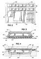
- FIG. 7illustrates a frontside plan view of an exemplary embodiment of a substrate in accordance with the present invention
- FIG. 8illustrates a frontside plan view of an exemplary embodiment of a die mounted substrate in accordance with the present invention
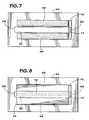
- FIG. 9illustrates a backside plan view of an exemplary embodiment of a die mounted substrate in accordance with the present invention.
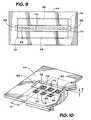
- FIG. 10illustrates a backside perspective view of an exemplary embodiment of a die mounted substrate in accordance with the present invention.
- FIG. 1a block diagram depicting an exemplary processor-based device, generally designated by the reference numeral 10 , is illustrated.
- the device 10may be any of a variety of different types, such as a computer, pager, cellular telephone, personal organizer, control circuit, etc.
- a processor 12such as a microprocessor, controls many of the functions of the device 10 .
- the device 10typically includes a power supply 14 .
- the power supply 14would advantageously include permanent batteries, replaceable batteries, and/or rechargeable batteries.
- the power supply 14may also include an A/C adapter, so that the device may be plugged into a wall outlet, for instance.
- the power supply 14may also include a D/C adapter, so that the device 10 may be plugged into a vehicle's cigarette lighter, for instance.
- a user interface 16may be coupled to the processor 12 .
- the user interface 16may include buttons, switches, a keyboard, a light pin, a mouse, and/or a voice recognition system, for instance.
- a display 18may also be coupled to the processor 12 .
- the display 18may include an LCD display, a CRT, LEDs, and/or an audio display.
- an RF subsystem/baseband processor 20may also be coupled to the processor 12 .
- the RF subsystem/baseband processor 20may include an antenna that is coupled to an RF receiver and to an RF transmitter (not shown).
- a communications port 22may also be coupled to the processor 12 .
- the communications port 22may be adapted to be coupled to a peripheral device 24 , such as a modem, a printer, or a computer, for instance, or to a network, such as a local area network or the Internet.
- memoryis coupled to the processor 12 to store and facilitate execution of the program.
- the processor 12may be coupled to volatile memory 26 , which may include dynamic random access memory (DRAM) and/or static random access memory (SRAM).
- the processor 12may also be coupled to non-volatile memory 28 .
- the non-volatile memory 28may include a read only memory (ROM), such as an EPROM or Flash-Memory, to be used in conjunction with the volatile memory.
- ROMread only memory
- the size of the ROMis typically selected to be just large enough to store any necessary operating system, application programs, and fixed data.
- the volatile memoryon the other hand, is typically quite large so that it can store dynamically loaded applications.
- the non-volatile memory 28may include a high capacity memory such as a disk or tape drive memory.
- a circuit board 30having various devices and connections coupled to its surface.
- a microprocessor 32is shown along with a ROM device 34 and a set of memory modules 36 , each containing a plurality of RAM chips 38 .
- a plurality of connections or ports 40are also located on the circuit board 30 allowing for connection to various peripheral devices and expansion modules.
- such devices and expansion modulesmight include sound cards, video cards, additional memory modules or connections for input and output peripherals.
- the present embodimenthas a direct relation to memory chips such as the ROM device 34 and RAM chip 38 , the techniques described below, may be applied to any device package having similar mounting characteristics including, if desired, the microprocessor 32 .
- ROM device 34is depicted as a typical BGA device.
- the BGA deviceincludes a chip or die 42 adhered to a substrate 44 .
- the dieis a semiconducting device typically having a plurality of transistors, capacitors, and/or electrical connections.
- Die 42is attached to substrate 44 by adhesive 48 .
- the adhesive 48in this particular embodiment is tape.
- the die 42 tactis typically encapsulated in a molding compound 46 .
- the molding compound 46is typically a resin.
- the molding compound 46is also disposed on the backside of the substrate 44 to protect bond wire connections (not shown) between the die 42 and substrates 44 , as will be described below herein.
- the molding compound 46 on the backside of substrate 44will also reduce bowing of the substrate 44 caused by the molding compound 46 on the frontside of substrate 44 .
- a plurality of conductive balls 50are arranged in an array on the surface of the substrate opposite the die 42 .
- the conductive balls 50are typically formed of solder.
- the conductive balls 52are electrically connected through the substrate to wire bonds (not shown) extending from the die.
- the device 34is placed onto a circuit board 30 having bond pads (not shown). The bond pads are arranged to mirror the array pattern of the conductive balls 50 .
- the device 34is attached to the circuit board 30 by reflowing the solder to create an electrical connection between the conductive balls 50 and the bond pads of the circuit board 30 . While FIG. 3 depicts a typical BGA device, it should be evident that the techniques described herein may be applied to devices which are subject to other surface mounting techniques.
- the substrate 44is typically adhered to die 42 by adhesive tape 48 .
- the substrate 44 and die 42are placed in a molding cavity 52 with the die 42 on the bottom side.
- a molding compoundis introduced into the molding cavity 52 by a mold gate 54 located at an edge of the substrate 44 . It is desirable that the molding compound flows as shown by directional arrows 56 , 58 , and 60 .
- the molding compoundfirst flows in through the mold gate 54 in the direction indicated by arrow 56 .
- the molding compoundflows around the die 42 as indicated by arrow 58 , and then up through the slot 62 into the molding cavity 64 as indicated by directional arrow 60 .
- the slot 62is a section which has been cut through the substrate 44 , as is better illustrated in FIGS. 5-9.
- the dashed lines 66 and 68 in the substrate 44 in FIG. 4represent the ends of the slot 62 .
- the slot 62is filled with the molding compound to provide protection for the electrical connects between the die 42 and the substrate 44 .
- the electrical connectionsare made by bond wires (not shown), but other suitable means of providing electrical conductivity may be used.
- FIG. 5illustrates a top plan view of a typical semiconductor device.
- the die 42is coupled to the substrate 44 using adhesive tape 48 .
- the substrate 44contains a slot 62 .
- the die 42is coupled to the substrate 44 , it is mounted in such a way that bond pads 70 on the backside of die 42 are aligned over the slot 62 . This enables the die 42 to be electrically coupled to the substrate 44 using bond wires (not shown).
- the die 42is typically mounted to the substrate 44 in such a way as to leave portions of the slot 62 exposed. The reason for leaving the slot 62 partially exposed is to facilitate the encapsulation process as shown in FIG. 4 . Thus, in FIG. 5 the die 42 is mounted in such a way as to leave slot end 66 and slot end 68 exposed.
- the flow path of the molding compoundis not controlled since the molding compound may flow from the die side of the substrate 44 to the backside of the substrate 44 through slot region 72 or slot region 74 during the encapsulation process.
- the lack of flow path controlmay lead to improper cooling, incomplete mold fill, mold bleed, discontinuities in the final mold, and/or electrical bridging.
- one end of the slot 62may be covered.
- a certain distance Xis necessary between the first bond pad 70 and the ends of the slot 62 so that the capillary used in the automated bonding process may reach the bond pads 70 without being driven into the edges of the substrate 44 .
- the bonding processis discussed more fully herein with reference to FIG. 9 .
- FIG. 6One solution to this problem is illustrated in FIG. 6 .
- the die 42is increased in size in order to cover distance X. While this solution will allow the proper clearance necessary for the wire bond process, it wastes valuable space on the die 42 by providing space which cannot be occupied by a bond pad 70 . During the encapsulation process, all molding compound will flow uniformly through an opening 72 in the slot 62 .
- FIG. 7illustrates a top plan view of this embodiment.
- the substrate 44is shown without the die 42 attached.
- the slot 62is cut through the substrate 44 .
- Adhesive tape 48is disposed on either side of the slot 62 to couple the die 42 to the substrate 44 .
- an additional strip of tape 76is placed over the opening 74 of the slot 62 .
- the covered slot opening 74 and the width of tape 76are at least as wide as distance X (illustrated in FIGS. 5 and 6) to provide the space to allow the capillary to clear the substrate during the wire bond process.
- FIG. 8illustrates the same top plan view of the substrate 44 as illustrated in FIG. 7 .
- the die 42is now attached to the substrate 44 .
- bond pads 70may be disposed on the backside of the die 42 without concern of wire bond process design rules.
- a strip of tape 76is used.
- FIG. 9illustrates a backside view of the substrate 44 as depicted in FIG. 8 .
- bond pads 70are arranged in such a way as to allow bond wires (not shown) to electrically couple the die 42 to the substrate 44 .
- an automated bond machineis used to attach gold wires from pads 70 on the die 42 to the substrate 44 .
- the capillary on the automated bonding equipmentrequires that nothing obstruct be path to the bond pads 70 .
- the wall edges created in the substrate 44 by the slot 62are advantageously at least a distance X from the center of the outermost pad 70 .
- FIG. 10illustrates a backside perspective view of the substrate 44 .
- pads 70 on the die 42are electrically coupled to bond pads 78 on the substrate 44 by bond wires 80 .
- an automated bonderis typically used to attach bond wires 80 to the bond pads 70 and 78 .
- the slot 62has some depth D associated with it that is equal to a thickness of the substrate 44 , it is useful to ensure that the bonding capillary has sufficient clearance from the slot edge 68 to ensure that the capillary does not hit the substrate during the bonding process.
- wire bond design rulesspecify a minimum distance M from the edge of a wall, such as it created by the slot 62 in the substrate 44 , to bond pad 70 .
- the minimum distance Mwill depend on the depth D of the cavity and the particular capillary used by the wire bond equipment.
- tape 76may be applied to space the die 42 adequately from the slot edge 68 without creating an opening to allow for an uncontrolled flow path of the molding compound.
- the substrate 44is a molded substrate, it may be possible to provide a small shelf at the end of the slot 62 which also blocks the end of the cavity 62 using the same material from which the substrate 44 is manufactured.
Landscapes
- Engineering & Computer Science (AREA)
- Microelectronics & Electronic Packaging (AREA)
- Physics & Mathematics (AREA)
- Condensed Matter Physics & Semiconductors (AREA)
- General Physics & Mathematics (AREA)
- Computer Hardware Design (AREA)
- Power Engineering (AREA)
- Manufacturing & Machinery (AREA)
- Encapsulation Of And Coatings For Semiconductor Or Solid State Devices (AREA)
- Structures Or Materials For Encapsulating Or Coating Semiconductor Devices Or Solid State Devices (AREA)
Abstract
Description
Claims (20)
Priority Applications (4)
| Application Number | Priority Date | Filing Date | Title |
|---|---|---|---|
| US09/520,260US6577015B1 (en) | 2000-03-07 | 2000-03-07 | Partial slot cover for encapsulation process |
| US10/421,133US6984894B2 (en) | 2000-03-07 | 2003-04-23 | Semiconductor package having a partial slot cover for encapsulation process |
| US10/421,137US6790708B2 (en) | 2000-03-07 | 2003-04-23 | Encapsulation process using a partial slot cover and a package formed by the process |
| US11/216,786US20060049531A1 (en) | 2000-03-07 | 2005-08-31 | Semiconductor package having a partial slot cover for encapsulation process |
Applications Claiming Priority (1)
| Application Number | Priority Date | Filing Date | Title |
|---|---|---|---|
| US09/520,260US6577015B1 (en) | 2000-03-07 | 2000-03-07 | Partial slot cover for encapsulation process |
Related Child Applications (2)
| Application Number | Title | Priority Date | Filing Date |
|---|---|---|---|
| US10/421,137DivisionUS6790708B2 (en) | 2000-03-07 | 2003-04-23 | Encapsulation process using a partial slot cover and a package formed by the process |
| US10/421,133DivisionUS6984894B2 (en) | 2000-03-07 | 2003-04-23 | Semiconductor package having a partial slot cover for encapsulation process |
Publications (1)
| Publication Number | Publication Date |
|---|---|
| US6577015B1true US6577015B1 (en) | 2003-06-10 |
Family
ID=24071832
Family Applications (4)
| Application Number | Title | Priority Date | Filing Date |
|---|---|---|---|
| US09/520,260Expired - LifetimeUS6577015B1 (en) | 2000-03-07 | 2000-03-07 | Partial slot cover for encapsulation process |
| US10/421,133Expired - LifetimeUS6984894B2 (en) | 2000-03-07 | 2003-04-23 | Semiconductor package having a partial slot cover for encapsulation process |
| US10/421,137Expired - Fee RelatedUS6790708B2 (en) | 2000-03-07 | 2003-04-23 | Encapsulation process using a partial slot cover and a package formed by the process |
| US11/216,786AbandonedUS20060049531A1 (en) | 2000-03-07 | 2005-08-31 | Semiconductor package having a partial slot cover for encapsulation process |
Family Applications After (3)
| Application Number | Title | Priority Date | Filing Date |
|---|---|---|---|
| US10/421,133Expired - LifetimeUS6984894B2 (en) | 2000-03-07 | 2003-04-23 | Semiconductor package having a partial slot cover for encapsulation process |
| US10/421,137Expired - Fee RelatedUS6790708B2 (en) | 2000-03-07 | 2003-04-23 | Encapsulation process using a partial slot cover and a package formed by the process |
| US11/216,786AbandonedUS20060049531A1 (en) | 2000-03-07 | 2005-08-31 | Semiconductor package having a partial slot cover for encapsulation process |
Country Status (1)
| Country | Link |
|---|---|
| US (4) | US6577015B1 (en) |
Families Citing this family (7)
| Publication number | Priority date | Publication date | Assignee | Title |
|---|---|---|---|---|
| US6577015B1 (en)* | 2000-03-07 | 2003-06-10 | Micron Technology, Inc. | Partial slot cover for encapsulation process |
| US20040022038A1 (en)* | 2002-07-31 | 2004-02-05 | Intel Corporation | Electronic package with back side, cavity mounted capacitors and method of fabrication therefor |
| US7521297B2 (en)* | 2006-03-17 | 2009-04-21 | Stats Chippac Ltd. | Multichip package system |
| JP5210613B2 (en)* | 2006-12-27 | 2013-06-12 | 株式会社半導体エネルギー研究所 | Semiconductor device |
| US7612444B2 (en)* | 2007-01-05 | 2009-11-03 | Stats Chippac, Inc. | Semiconductor package with flow controller |
| US8744391B2 (en)* | 2007-05-31 | 2014-06-03 | Motorola Mobility Llc | Signal strength indication methods for use in wireless communication devices |
| US8946901B2 (en) | 2013-01-22 | 2015-02-03 | Invensas Corporation | Microelectronic package and method of manufacture thereof |
Citations (12)
| Publication number | Priority date | Publication date | Assignee | Title |
|---|---|---|---|---|
| US5173766A (en)* | 1990-06-25 | 1992-12-22 | Lsi Logic Corporation | Semiconductor device package and method of making such a package |
| US5571027A (en)* | 1993-10-29 | 1996-11-05 | Texas Instruments Incorporated | Non-destructive interconnect system for semiconductor devices |
| US5854740A (en)* | 1995-04-27 | 1998-12-29 | Lg Semicon Co., Ltd. | Electronic circuit board with semiconductor chip mounted thereon, and manufacturing method therefor |
| US6127726A (en)* | 1999-05-27 | 2000-10-03 | Lsi Logic Corporation | Cavity down plastic ball grid array multi-chip module |
| US6224936B1 (en)* | 1998-10-07 | 2001-05-01 | Micron Technology, Inc. | Method for reducing warpage during application and curing of encapsulant materials on a printed circuit board |
| US6232148B1 (en)* | 1996-06-17 | 2001-05-15 | Micron Technology, Inc. | Method and apparatus leads-between-chips |
| US6246247B1 (en)* | 1994-11-15 | 2001-06-12 | Formfactor, Inc. | Probe card assembly and kit, and methods of using same |
| US6300163B1 (en)* | 1996-06-26 | 2001-10-09 | Micron Technology, Inc. | Stacked leads-over-chip multi-chip module |
| US6300165B2 (en)* | 1999-11-15 | 2001-10-09 | Substrate Technologies Incorporated | Ball grid substrate for lead-on-chip semiconductor package |
| US6331939B1 (en)* | 1998-05-04 | 2001-12-18 | Micron Technology, Inc. | Stackable ball grid array package |
| US6373127B1 (en)* | 1998-09-29 | 2002-04-16 | Texas Instruments Incorporated | Integrated capacitor on the back of a chip |
| US6388199B1 (en)* | 2000-07-31 | 2002-05-14 | Micron Technology, Inc. | Selectively adjusting surface tension of soldermask material |
Family Cites Families (11)
| Publication number | Priority date | Publication date | Assignee | Title |
|---|---|---|---|---|
| WO1991016656A1 (en)* | 1990-04-24 | 1991-10-31 | Seiko Epson Corporation | Semiconductor device provided with circuit cell and array, and data input-output device |
| US5353195A (en)* | 1993-07-09 | 1994-10-04 | General Electric Company | Integral power and ground structure for multi-chip modules |
| IT1272817B (en)* | 1994-08-24 | 1997-06-30 | Consorzio Eagle | PROCEDURE FOR THE ASSEMBLY OF INTEGRATED CIRCUITS ON PANELS OF PRINTED CIRCUITS |
| JPH08317605A (en)* | 1995-05-15 | 1996-11-29 | Mitsubishi Electric Corp | Molded motor |
| KR100248792B1 (en)* | 1996-12-18 | 2000-03-15 | 김영환 | Chip-Size Package Semiconductor Using Single Layer Ceramic Substrates |
| US6294825B1 (en)* | 1999-02-22 | 2001-09-25 | Micron Technology, Inc. | Asymmetrical mold of multiple-part matrixes |
| US6331936B1 (en)* | 1999-04-14 | 2001-12-18 | Dell Usa, L.P. | AC adapter for a module bay in a computer system |
| US6362964B1 (en)* | 1999-11-17 | 2002-03-26 | International Rectifier Corp. | Flexible power assembly |
| US6577015B1 (en)* | 2000-03-07 | 2003-06-10 | Micron Technology, Inc. | Partial slot cover for encapsulation process |
| US6548764B1 (en)* | 2000-06-07 | 2003-04-15 | Micron Technology, Inc. | Semiconductor packages and methods for making the same |
| SG95651A1 (en)* | 2001-05-21 | 2003-04-23 | Micron Technology Inc | Method for encapsulating intermediate conductive elements connecting a semiconductor die to a substrate and semiconductor devices so packaged |
- 2000
- 2000-03-07USUS09/520,260patent/US6577015B1/ennot_activeExpired - Lifetime
- 2003
- 2003-04-23USUS10/421,133patent/US6984894B2/ennot_activeExpired - Lifetime
- 2003-04-23USUS10/421,137patent/US6790708B2/ennot_activeExpired - Fee Related
- 2005
- 2005-08-31USUS11/216,786patent/US20060049531A1/ennot_activeAbandoned
Patent Citations (12)
| Publication number | Priority date | Publication date | Assignee | Title |
|---|---|---|---|---|
| US5173766A (en)* | 1990-06-25 | 1992-12-22 | Lsi Logic Corporation | Semiconductor device package and method of making such a package |
| US5571027A (en)* | 1993-10-29 | 1996-11-05 | Texas Instruments Incorporated | Non-destructive interconnect system for semiconductor devices |
| US6246247B1 (en)* | 1994-11-15 | 2001-06-12 | Formfactor, Inc. | Probe card assembly and kit, and methods of using same |
| US5854740A (en)* | 1995-04-27 | 1998-12-29 | Lg Semicon Co., Ltd. | Electronic circuit board with semiconductor chip mounted thereon, and manufacturing method therefor |
| US6232148B1 (en)* | 1996-06-17 | 2001-05-15 | Micron Technology, Inc. | Method and apparatus leads-between-chips |
| US6300163B1 (en)* | 1996-06-26 | 2001-10-09 | Micron Technology, Inc. | Stacked leads-over-chip multi-chip module |
| US6331939B1 (en)* | 1998-05-04 | 2001-12-18 | Micron Technology, Inc. | Stackable ball grid array package |
| US6373127B1 (en)* | 1998-09-29 | 2002-04-16 | Texas Instruments Incorporated | Integrated capacitor on the back of a chip |
| US6224936B1 (en)* | 1998-10-07 | 2001-05-01 | Micron Technology, Inc. | Method for reducing warpage during application and curing of encapsulant materials on a printed circuit board |
| US6127726A (en)* | 1999-05-27 | 2000-10-03 | Lsi Logic Corporation | Cavity down plastic ball grid array multi-chip module |
| US6300165B2 (en)* | 1999-11-15 | 2001-10-09 | Substrate Technologies Incorporated | Ball grid substrate for lead-on-chip semiconductor package |
| US6388199B1 (en)* | 2000-07-31 | 2002-05-14 | Micron Technology, Inc. | Selectively adjusting surface tension of soldermask material |
Also Published As
| Publication number | Publication date |
|---|---|
| US6984894B2 (en) | 2006-01-10 |
| US6790708B2 (en) | 2004-09-14 |
| US20060049531A1 (en) | 2006-03-09 |
| US20030178731A1 (en) | 2003-09-25 |
| US20030205805A1 (en) | 2003-11-06 |
Similar Documents
| Publication | Publication Date | Title |
|---|---|---|
| US6979904B2 (en) | Integrated circuit package having reduced interconnects | |
| US9559087B2 (en) | Techniques for packaging multiple device components | |
| US6503781B2 (en) | Molded ball grid array | |
| US7951646B2 (en) | Solder ball landpad design to improve laminate performance | |
| US7122404B2 (en) | Techniques for packaging a multiple device component | |
| US6486536B1 (en) | U-shape tape for BOC FBGA package to improve moldability | |
| US6791198B2 (en) | Method and apparatus for gate blocking X-outs during a molding process | |
| US6889430B2 (en) | Method of selectively adjusting surface tension of soldermask material | |
| US6577015B1 (en) | Partial slot cover for encapsulation process | |
| US6916683B2 (en) | Methods of fabricating a molded ball grid array | |
| US6691406B2 (en) | Methods of die attachment for BOC and F/C surface mount | |
| US7054161B1 (en) | Slotted adhesive for die-attach in BOC and LOC packages | |
| US6473311B1 (en) | Gate area relief strip for a molded I/C package |
Legal Events
| Date | Code | Title | Description |
|---|---|---|---|
| AS | Assignment | Owner name:MICRON TECHNOLOGY, INC., IDAHO Free format text:ASSIGNMENT OF ASSIGNORS INTEREST;ASSIGNOR:RUMSEY, BRAD D.;REEL/FRAME:010669/0100 Effective date:20000301 | |
| STCF | Information on status: patent grant | Free format text:PATENTED CASE | |
| FEPP | Fee payment procedure | Free format text:PAYOR NUMBER ASSIGNED (ORIGINAL EVENT CODE: ASPN); ENTITY STATUS OF PATENT OWNER: LARGE ENTITY | |
| FPAY | Fee payment | Year of fee payment:4 | |
| FPAY | Fee payment | Year of fee payment:8 | |
| FPAY | Fee payment | Year of fee payment:12 | |
| AS | Assignment | Owner name:U.S. BANK NATIONAL ASSOCIATION, AS COLLATERAL AGENT, CALIFORNIA Free format text:SECURITY INTEREST;ASSIGNOR:MICRON TECHNOLOGY, INC.;REEL/FRAME:038669/0001 Effective date:20160426 Owner name:U.S. BANK NATIONAL ASSOCIATION, AS COLLATERAL AGEN Free format text:SECURITY INTEREST;ASSIGNOR:MICRON TECHNOLOGY, INC.;REEL/FRAME:038669/0001 Effective date:20160426 | |
| AS | Assignment | Owner name:MORGAN STANLEY SENIOR FUNDING, INC., AS COLLATERAL AGENT, MARYLAND Free format text:PATENT SECURITY AGREEMENT;ASSIGNOR:MICRON TECHNOLOGY, INC.;REEL/FRAME:038954/0001 Effective date:20160426 Owner name:MORGAN STANLEY SENIOR FUNDING, INC., AS COLLATERAL Free format text:PATENT SECURITY AGREEMENT;ASSIGNOR:MICRON TECHNOLOGY, INC.;REEL/FRAME:038954/0001 Effective date:20160426 | |
| AS | Assignment | Owner name:U.S. BANK NATIONAL ASSOCIATION, AS COLLATERAL AGENT, CALIFORNIA Free format text:CORRECTIVE ASSIGNMENT TO CORRECT THE REPLACE ERRONEOUSLY FILED PATENT #7358718 WITH THE CORRECT PATENT #7358178 PREVIOUSLY RECORDED ON REEL 038669 FRAME 0001. ASSIGNOR(S) HEREBY CONFIRMS THE SECURITY INTEREST;ASSIGNOR:MICRON TECHNOLOGY, INC.;REEL/FRAME:043079/0001 Effective date:20160426 Owner name:U.S. BANK NATIONAL ASSOCIATION, AS COLLATERAL AGEN Free format text:CORRECTIVE ASSIGNMENT TO CORRECT THE REPLACE ERRONEOUSLY FILED PATENT #7358718 WITH THE CORRECT PATENT #7358178 PREVIOUSLY RECORDED ON REEL 038669 FRAME 0001. ASSIGNOR(S) HEREBY CONFIRMS THE SECURITY INTEREST;ASSIGNOR:MICRON TECHNOLOGY, INC.;REEL/FRAME:043079/0001 Effective date:20160426 | |
| AS | Assignment | Owner name:JPMORGAN CHASE BANK, N.A., AS COLLATERAL AGENT, ILLINOIS Free format text:SECURITY INTEREST;ASSIGNORS:MICRON TECHNOLOGY, INC.;MICRON SEMICONDUCTOR PRODUCTS, INC.;REEL/FRAME:047540/0001 Effective date:20180703 Owner name:JPMORGAN CHASE BANK, N.A., AS COLLATERAL AGENT, IL Free format text:SECURITY INTEREST;ASSIGNORS:MICRON TECHNOLOGY, INC.;MICRON SEMICONDUCTOR PRODUCTS, INC.;REEL/FRAME:047540/0001 Effective date:20180703 | |
| AS | Assignment | Owner name:MICRON TECHNOLOGY, INC., IDAHO Free format text:RELEASE BY SECURED PARTY;ASSIGNOR:U.S. BANK NATIONAL ASSOCIATION, AS COLLATERAL AGENT;REEL/FRAME:047243/0001 Effective date:20180629 | |
| AS | Assignment | Owner name:MICRON TECHNOLOGY, INC., IDAHO Free format text:RELEASE BY SECURED PARTY;ASSIGNOR:MORGAN STANLEY SENIOR FUNDING, INC., AS COLLATERAL AGENT;REEL/FRAME:050937/0001 Effective date:20190731 | |
| AS | Assignment | Owner name:MICRON TECHNOLOGY, INC., IDAHO Free format text:RELEASE BY SECURED PARTY;ASSIGNOR:JPMORGAN CHASE BANK, N.A., AS COLLATERAL AGENT;REEL/FRAME:051028/0001 Effective date:20190731 Owner name:MICRON SEMICONDUCTOR PRODUCTS, INC., IDAHO Free format text:RELEASE BY SECURED PARTY;ASSIGNOR:JPMORGAN CHASE BANK, N.A., AS COLLATERAL AGENT;REEL/FRAME:051028/0001 Effective date:20190731 |