US6576932B2 - Increasing the brightness of III-nitride light emitting devices - Google Patents
Increasing the brightness of III-nitride light emitting devicesDownload PDFInfo
- Publication number
- US6576932B2 US6576932B2US09/797,770US79777001AUS6576932B2US 6576932 B2US6576932 B2US 6576932B2US 79777001 AUS79777001 AUS 79777001AUS 6576932 B2US6576932 B2US 6576932B2
- Authority
- US
- United States
- Prior art keywords
- base layer
- substrate
- micrometers
- light emitting
- thickness
- Prior art date
- Legal status (The legal status is an assumption and is not a legal conclusion. Google has not performed a legal analysis and makes no representation as to the accuracy of the status listed.)
- Expired - Lifetime
Links
Images


Classifications
- H—ELECTRICITY
- H01—ELECTRIC ELEMENTS
- H01L—SEMICONDUCTOR DEVICES NOT COVERED BY CLASS H10
- H01L21/00—Processes or apparatus adapted for the manufacture or treatment of semiconductor or solid state devices or of parts thereof
- H01L21/02—Manufacture or treatment of semiconductor devices or of parts thereof
- H01L21/02104—Forming layers
- H01L21/02365—Forming inorganic semiconducting materials on a substrate
- H01L21/02518—Deposited layers
- H01L21/02521—Materials
- H01L21/02538—Group 13/15 materials
- H01L21/0254—Nitrides
- H—ELECTRICITY
- H01—ELECTRIC ELEMENTS
- H01L—SEMICONDUCTOR DEVICES NOT COVERED BY CLASS H10
- H01L21/00—Processes or apparatus adapted for the manufacture or treatment of semiconductor or solid state devices or of parts thereof
- H01L21/02—Manufacture or treatment of semiconductor devices or of parts thereof
- H01L21/02104—Forming layers
- H01L21/02365—Forming inorganic semiconducting materials on a substrate
- H01L21/02367—Substrates
- H01L21/0237—Materials
- H—ELECTRICITY
- H01—ELECTRIC ELEMENTS
- H01L—SEMICONDUCTOR DEVICES NOT COVERED BY CLASS H10
- H01L21/00—Processes or apparatus adapted for the manufacture or treatment of semiconductor or solid state devices or of parts thereof
- H01L21/02—Manufacture or treatment of semiconductor devices or of parts thereof
- H01L21/02104—Forming layers
- H01L21/02365—Forming inorganic semiconducting materials on a substrate
- H01L21/02367—Substrates
- H01L21/02433—Crystal orientation
- H—ELECTRICITY
- H01—ELECTRIC ELEMENTS
- H01L—SEMICONDUCTOR DEVICES NOT COVERED BY CLASS H10
- H01L21/00—Processes or apparatus adapted for the manufacture or treatment of semiconductor or solid state devices or of parts thereof
- H01L21/02—Manufacture or treatment of semiconductor devices or of parts thereof
- H01L21/02104—Forming layers
- H01L21/02365—Forming inorganic semiconducting materials on a substrate
- H01L21/02436—Intermediate layers between substrates and deposited layers
- H01L21/02439—Materials
- H01L21/02455—Group 13/15 materials
- H01L21/02458—Nitrides
- H—ELECTRICITY
- H10—SEMICONDUCTOR DEVICES; ELECTRIC SOLID-STATE DEVICES NOT OTHERWISE PROVIDED FOR
- H10H—INORGANIC LIGHT-EMITTING SEMICONDUCTOR DEVICES HAVING POTENTIAL BARRIERS
- H10H20/00—Individual inorganic light-emitting semiconductor devices having potential barriers, e.g. light-emitting diodes [LED]
- H10H20/01—Manufacture or treatment
- H10H20/011—Manufacture or treatment of bodies, e.g. forming semiconductor layers
- H10H20/013—Manufacture or treatment of bodies, e.g. forming semiconductor layers having light-emitting regions comprising only Group III-V materials
- H10H20/0133—Manufacture or treatment of bodies, e.g. forming semiconductor layers having light-emitting regions comprising only Group III-V materials with a substrate not being Group III-V materials
- H10H20/01335—Manufacture or treatment of bodies, e.g. forming semiconductor layers having light-emitting regions comprising only Group III-V materials with a substrate not being Group III-V materials the light-emitting regions comprising nitride materials
- H—ELECTRICITY
- H10—SEMICONDUCTOR DEVICES; ELECTRIC SOLID-STATE DEVICES NOT OTHERWISE PROVIDED FOR
- H10H—INORGANIC LIGHT-EMITTING SEMICONDUCTOR DEVICES HAVING POTENTIAL BARRIERS
- H10H20/00—Individual inorganic light-emitting semiconductor devices having potential barriers, e.g. light-emitting diodes [LED]
- H10H20/80—Constructional details
- H10H20/81—Bodies
- H10H20/817—Bodies characterised by the crystal structures or orientations, e.g. polycrystalline, amorphous or porous
Definitions
- the present inventionrelates to increasing the brightness of III-Nitride light emitting diodes.
- LEDsLight emitting diodes
- Direct bandgap semiconductorsare the materials of choice for fabrication of LEDs, which generate light from electricity.
- One important class of light emitting systemsare based upon compound alloys of Group III atoms (particularly In, Ga, Al) and nitrogen N, typically abbreviated as “III-Nitrides.”
- III-Nitride compoundsOne family of III-Nitride compounds has the general composition (In x Ga l-x ) y Al l-y N where 0 ⁇ (x,y) ⁇ 1.
- III-Nitridesare capable of emitting light that spans a large portion of the visible and near-ultraviolet electromagnetic spectrum including ultraviolet, blue, green, yellow and red wavelengths. Improving the brightness and other optical properties of LEDs is an important technological goal.
- FIG. 1A portion of a typical prior art LED structure is depicted in FIG. 1 .
- Other components of LEDs as known in the artare omitted for clarity.
- An LEDtypically has one or more layers epitaxially deposited on a surface of a substrate prior to the formation of the light emitting active region. These epitaxial layers form a “base layer” that can have n-type conductivity.
- FIG. 1depicts an example of a base layer having a GaN layer beneath an n-type GaN layer.
- the light emitting active region in which radiative recombination of electrons and holes occursis formed on top of the base layer, typically in the form of at least one quantum well although single and double heterostructures and homojunctions can also be used. Above the active region lie p-type conductive injection and confinement regions. Positive and negative contacts (omitted from FIG. 1) are also provided.
- the present inventionrelates to structures for light emitting devices, particularly LEDs employing a III-Nitride light emitting active region deposited on an n-type conductive base layer.
- the substrate upon which the base layer is grownis cut intentionally misaligned from a main crystal plane.
- base layersare employed that are thicker than 3.5 ⁇ m.
- the presence of a thick base layerprovides sufficient mechanical support for the device such that the substrate can be removed entirely from the light emitting system, further increasing the performance of the device.
- Examplesare provided for the illustrative case of thick base layers deposited on a sapphire substrate misaligned from the c-axis. Misalignment angles are in the range from 0.05° to approximately 0.50.
- the present inventionalso employs base layers thicker than 3.5 ⁇ m, preferably in the range of 7 ⁇ m-10 ⁇ m. The combination of base layers>3.5 ⁇ m, grown on the misaligned substrates leads to surprisingly improved light emission.
- FIG. 1Schematic cross-sectional depiction of a portion of a prior art LED layered structure.
- FIG. 2Schematic depiction of a sapphire unit cell.
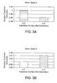
- FIGS. 3 a and 3 bRelative light emitting efficiency for LEDs grown on mis-oriented c-plane sapphire substrates with mis-orientation angles of 0.3 and 0.5°. Data are shown for LED structures with base layers having strain state A (a) and B (b).
- FIG. 4Schematic cross-sectional depiction of a portion of a LED layered structure pursuant to an embodiment of the present invention.
- FIG. 5Schematic cross-sectional depiction of a portion of a LED layered structure pursuant to another embodiment of the present invention.
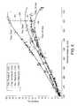
- FIG. 6Brightness as a function of dominant wavelength for LEDs having thin (3.5 ⁇ m) and thick (6.5 ⁇ m) base layers grown on-axis (tilt angle less than 0.05°) and off-axis (tilt angle in the range from about 0.20° to about 0.40°).
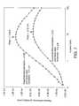
- FIG. 7Relative light emitting efficiency as a function of forward current for the thick base layer (6.5 ⁇ m) LED depicted in FIG. 5 grown on-axis (0.03°) and off-axis (0.39°).
- FIG. 8Brightness as a function of dominant wavelength for four experiments of the same device structure grown with a thick base layer (6.5 ⁇ m) on substrates with and without misalignment.
- FIG. 9Display device incorporating the high brightness LEDs of the present invention.
- the present inventionrelates to epitaxial layer thickness and crystal orientation for light emitting diodes (“LEDs”) and, in particular to the substrate orientation and the base layer thickness between the substrate and the light emitting active region resulting in improved light emitting properties.
- the base layeris the layer or layers between the substrate and the active region, including layers close to the substrate, such as buffer or nucleation layers and layers close to the active region, such as transition layers. Specific examples are included in connection with LEDs based upon a double heterostructure multiple quantum well light emitting active region composed of indium gallium nitride (InGaN) deposited on an n-type conductive base layer on a sapphire substrate. These examples are intended to be illustrative only.
- the present inventionis applicable to homojunctions, to single and double heterostructures and to single or multiple quantum well embodiments.
- the substrateis cut intentionally misaligned from a main crystal plane and thick base layers are grown on the misaligned substrates.
- Higher brightness and improved efficiencyare among the improvements demonstrated in various embodiments by off-axis growth of a thick base layer.
- One embodimentis the growth of a thick n-type GaN base layer on an off-axis sapphire substrate.
- the substrates upon which LEDs can be fabricatedinclude sapphire, SiC, GaN, GaAs, and GaP among others. Examples are included for the specific case of misaligned base layer growth on a sapphire substrate. However, sapphire is described herein as an illustrative example, not intended as a limitation on the various embodiments.
- FIG. 2depicts the structure of a unit cell of the sapphire crystal and the planes commonly designated a, c, m and r.
- the ⁇ 0001 ⁇ planeis designated the “c-plane,” and the “c-axis” is perpendicular to the c-plane.
- sapphire and III-Nitrideshave a large lattice mismatch.
- III-Nitride nucleation layeralso called a buffer layer
- the rest of the base layerthen can be deposited.
- the base layerprovides for carrier transport to the light emitting layer.
- the base layertypically comprises one or more III-Nitride materials (undoped, n-type or p-type).
- n-doped GaN base layerincluding doped, modestly doped, undoped and/or unintentionally doped GaN sublayers, recognizing that other materials can be employed for the base layer.
- a base layer with a graded dopingcan also be used.
- the doping level of the base layercan be lower in the direction towards the substrate and can be higher in the direction towards the active region, although the region close to the active region or the substrate may not follow this doping grade.
- Typical procedures for depositing n-type base layers, fabricating the MQW active region, and depositing p-type layersare described in several standard references including Introduction to Nitride Semiconductor Blue Lasers and Light Emitting Diodes , Eds. S. Nakamura and S. F.
- LEDsConventional fabrication techniques for LEDs involve the growth of one or more layers collectively comprising a base layer and providing a transition from the substrate to the active region.
- base layersare conventionally grown on the sapphire substrate along the c-axis, typically called “on-axis” or “aligned” growth. “On-axis” emphasizes that the sapphire crystal is cut as precisely as is feasible along the c crystallographic plane (or other main crystal plane) and the base layer is grown substantially perpendicular to the c-axis.
- the sapphire (or other) substrate upon which the base layer is grownis cut not precisely perpendicular to the c-axis depicted in FIG. 2 (or other main crystallographic axis) but is inclined at a small deviation from perpendicularity.
- the substrate surface on which the base layer is deposited pursuant to these embodimentsis thus not precisely the c-plane depicted in FIG. 2 .
- the direction of misalignment with respect to a designated crystallographic axiscan also be specified.
- m-plane tiltFor the examples considered herein of growth on a sapphire substrate, it is convenient to indicate the direction of misalignment of the c-axis towards the m-plane as “m-plane tilt,” or towards the a-plane as “a-plane tilt.”
- off-axis growth planescan have any orientation, not limited to purely m-plane or purely a-plane tilts.
- Off-axis growth for other substratescan be defined in a completely analogous manner in terms of the direction of the misalignment with respect to a main crystallographic axis.
- the layer being grownmay crack.
- the cracking limitis the maximum thickness that the layer (of a particular doping) can be grown without significant cracking, such that device performance is not adversely affected. There can be a trade-off between doping and thickness, the lighter the doping, the thicker the layer can be grown before it cracks.
- M-plane, a-plane and intermediate direction tilts from the c-planehave been investigated with respect to base layer growth on sapphire. No significant variation in optical performance has been observed with variation in tilt direction to the accuracy of the measurements reported herein.
- Most tilt angles given hereinare m-plane tilts from the c-plane. Tilt angles less than 0.05° are not significantly different from on-axis. Thus, “on-axis” is used herein to indicate tilt angles from 0 to 0.05° in any direction.
- a base layer comprising one or more constituent layersis typically grown on the substrate as a transition region between the substrate the light emitting active region.
- MOCVDMetal-Organic Chemical Vapor Deposition
- a base layeris typically grown on the substrate as a transition region between the substrate the light emitting active region.
- MOCVDMetal-Organic Chemical Vapor Deposition
- FIG. 4is a schematic depiction of the cross-section of a portion of an LED device pursuant to an embodiment of the present invention.
- the devicecomprises a base layer of AlInGaN grown above an off-axis substrate to a thickness greater than about 3.5 ⁇ m.
- the first layer or region of the base layeris typically a buffer layer or nucleation layer (not shown).
- the last layer or region of the base layercan be a transition layer (not shown), that can provide a transition between the previous base layer growth and the active region.
- An active region for emitting lightis grown above the base layer.
- the active regioncan be a homojunction, a single or a double heterostructure, or a single or multiple quantum well structure.
- An AlInGaN confinement layeris grown above the active region.
- the AlInGaN layerscan be any composition of AlInGaN, including GaN, AlGaN, and InGaN, and can be n-type, p-type, undoped, or have a graded doping profile.
- the two AlInGaN layerscan have different compositions from one another.
- the AlInGaN base layercan have a graded doping level that generally decreases in the direction towards the substrate and increases in the direction towards the active region, although as previously mentioned, other regions or layers close to the substrate or close to the active region may not follow this doping grade.
- the AlInGaN base layercan be composed of sublayers including a sublayer that is closer to the substrate and a sublayer that is closer to the active region such that the sublayer closer to the active region is more heavily doped than the sublayer closer to the substrate.
- the sublayer closer to the active regioncan be more heavily doped n-type or p-type than the sublayer closer to the substrate.
- sublayer dopingsinclude: a sublayer closer to the active region more heavily doped n-type than a n-type sublayer closer to the substrate; a sublayer closer to the active region more heavily p-type than a p-type sublayer closer to the substrate; a sublayer closer to the active region more heavily doped p-type than a n-type sublayer closer to the substrate; and a sublayer closer to the active region more heavily doped n-type than a p-type sublayer closer to the substrate.
- P-type base layers between the substrate and the active regioncan occur, for example, in tunnel junction devices and in n-up devices that that have an opposite polarity electric field than the more conventional p-up devices. All of these devices are included within the scope of the present invention.
- FIG. 5, one embodiment of the present inventionis a schematic depiction of the cross-section of a portion of an LED device showing a sapphire substrate 1 and the base layer 3 between the substrate and the light emitting active region 5 .
- a base layer of n-type GaN 2comprising a sublayer of the base layer 3 deposited on a buffer layer (not shown) on a sapphire substrate 1 misaligned from a main crystal plane.
- the buffer layer growth of nitride on sapphireis recognized not to be precisely epitaxial due to the lattice mismatch.
- nitride on sapphireRather, the initial stages in the growth of nitride on sapphire seem to proceed by solid phase crystallization from an amorphous phase of GaN as deposited on the sapphire.
- Subsequent base layersare deposited epitaxially on the buffer layer.
- the base layersare n-type GaN. If no special precautions are taken, deposited GaN tends to be n-type conductive. That is, if GaN is deposited without the introduction of specific dopants, n-type material typically results. This “unintentional” n-type doping may result from the incorporation of n-type impurities (for example, silicon and oxygen) from background gases into the GaN.
- n-type impuritiesfor example, silicon and oxygen
- n-doped GaNcan also be used as base sublayer 2 in which modest amounts of dopants are specifically introduced into the GaN. Specific introduction of modest amounts of dopant can result in a more controlled, reproducible LED structure than unintentional doping.
- sublayer 2is unintentionally doped n-type.
- doping levelshave an effect on the thickness to which sublayer 2 can be grown before the cracking limit is reached.
- lightly doped GaNindicates a GaN layer that is unintentionally or modestly doped having a doping level sufficiently low, typically less than about 5 ⁇ 10 8 dopant atoms per cubic centimeter.
- lightly doped sublayerallows the base layer to be grown to the desired thickness without reaching the cracking limit.
- lightly dopedapplied to material other than GaN used for sublayer 2 likewise denotes doping levels that allow growth to the desired thickness before the cracking level is reached.
- the lightly doped GaN 2 sublayeris 4.5 ⁇ m thick.
- n-doped GaN 4is grown over the lightly doped GaN 2 .
- n-doped GaN 4is 2 ⁇ m thick.
- N-GaN 4is typically doped to a concentration in the range of approximately 10 18 -10 20 dopant atoms per cubic centimeter.
- n-doped GaN 4has a dopant concentration on the order of approximately 10 19 dopant atoms per cubic centimeter.
- a Si dopantis used for the examples presented herein but is not a limitation on the scope of the present invention. Si, Ge, Sn, O are among the dopant atoms used to dope the III-Nitrides n-type.
- P-type dopantsinclude Mg, Zn, Be, C, and Cd.
- Another layer, layers, or regions of the base layer 3may precede the active region 5 .
- This transition layer or region(not shown) is part of base layer 3 and can be lightly doped and serves as a transition between the previous part of the base layer and the active region 5 .
- a multi-quantum-wellcomprising several quantum well layers separated by barrier layers of higher bandgap material.
- typical barrier layersinclude higher bandgap InGaN, GaN, AlGaN, and AlInGaN.
- Layers of p-type conductivity known as “confinement layers” and “injection layers”lie opposite the active region from the n-type base layer, depicted as 6 in FIG. 4 .
- Typical materials, dimensions and dopant concentrations for the p-layersare known in the art and given in the references previously cited and can be, for example, 100-1000 ⁇ of p-type Al x Ga l-x N (0 ⁇ 0.25) followed by 100-3000 ⁇ of p-type GaN.
- a more heavily doped p-type layermay be formed above the P-GaN to ensure good ohmic contact of the p-electrode.
- the base layersare grown on on-axis substrates with a total thickness of less than 3.5 ⁇ m.
- FIG. 5shows the base layer 3 , grown on off-axis substrates, to be thicker than that of FIG. 1 . That is, the present invention uses base layers 3 having a thickness greater than about 3.5 ⁇ m grown on off-axis substrates.
- a preferred thickness of base layer 3is from approximately 6.5 to approximately 9.5 ⁇ m grown on off-axis substrates.
- Improved brightnessis one favorable result from the use of thick base layers 3 in combination with off-axis epitaxial growth.
- we refer to “thin” and “thick” base layersto indicate the general ranges below 3.5 ⁇ m for “thin” and above 3.5 ⁇ m for “thick.”
- the examples presented hereinmaintain the N-GaN layer 4 at a thickness of about 2 ⁇ m and cause the base layer 3 to thicken by causing the lightly doped GaN layer 2 to thicken.
- base layers 3 thicker than about 3.5 ⁇ m and, advantageously, in the range from approximately 6.5 ⁇ m to about 9.5 ⁇ m grown on off-axis substratesgive adequate results in the practice of the present invention, considerably thicker layers up to approximately 200 ⁇ m grown off-axis are also feasible. Brightness increases with increasing thickness of the off-axis grown base layer and the present invention has no upper limit on thickness. However, the increased thickness of the overall LED structure tends to increase manufacturing complexities, for example throughput and device singulation.
- the primary function of the substrateis to provide a platform upon which the various layers of the complete light emitting device can be fabricated.
- the substratethus provides mechanical strength and stability during fabrication and operation.
- the optical properties of the substratemay interfere with effective light extraction (among other properties) and thus hinder device performance.
- the thick base layers used hereinprovide, in some cases, sufficient mechanical stability to allow separation of the substrate from the remainder of the device following fabrication of the thick base layers.
- the datarelates to InGaN MQW LEDs as generally depicted in FIG. 5 .
- FIG. 6depicts the LED brightness in lumens as a function of this dominant wavelength for LED's having thin and thick base layers. “Thin” base layers are about 3.5 ⁇ m thick while “thick” base layers are about 6.5 ⁇ m thick in FIG. 6 . Surprisingly, the improved light emission achieved by using thick and off-axis base layers in combination markedly exceeds the sum of the individual improvements from each effect considered separately. For example, at approximately 510 nm, FIG. 6 depicts the improvement obtained from thin on-axis to thick on-axis as segment 100 . The improvement achieved from thin on-axis to thin off-axis is depicted as 100+101.
- the combination of thick base layer together with growth on a on a off-axis substrateachieves an improvement in light emission that unexpectedly and clearly exceeds the sum of its individual parts.
- FIG. 7depicts the relative efficiency in producing light as a function of the forward current driving the LED.
- the datais not calibrated in terms of absolute light output (lumens) but rather compares the LED driving current with current generated by the particular photodetector employed to measure total light emitted.
- relative variations in light emitting efficiency from data point to data point and curve-to-curvemay be extracted from FIG. 7 .
- the data of FIG. 7relates to thick base layers as generally depicted in FIG. 5 (layer 3 approximately 6.5 ⁇ m), for two angles of misorientation from the c-axis towards the m-plane.
- the top curveis measured from a device grown on a substrate with a misalignment angle of approximately 0.39° and a base layer thickness of about 6.5 ⁇ m.
- the bottom curveis measured from a device grown on a on-axis substrate with a base layer thickness of about 6.5 ⁇ m.
- the off-axis depositionhas a higher maximum in the efficiency curve than does on-axis deposition.
- off-axis depositionis seen to peak at a lower current value than does on-axis deposition, 7.9 milliamp (mA) compared to 12.6 mA.
- FIG. 8depicts four experiments in which on-axis and off-axis sapphire substrates were loaded into the same reactor and LEDs fabricated under otherwise identical conditions. All experiments depicted in FIG. 8 employ thick base layers approximately 6.5 ⁇ m thick. Thus, FIG. 8 allows a clear comparison of the effect on light emission of tilted vs. untilted substrates for thick base layers pursuant to the present invention, removing effects of other experiment-to-experiment variations. FIG. 8 clearly depicts the enhanced brightness resulting from the growth of thick base layers on tilted substrates.
- the resulting high brightness LEDs formed in accordance with the inventionare particularly suitable for color display panels using red, green, and blue LEDs as the pixel elements.
- Such displaysare well known and are represented in FIG. 9.
- a display panel 300has an array of red, green, and blue LEDs, respectively, that are selectively illuminated by well known circuitry to display an image. Only three pixels are shown in FIG. 9 for simplicity.
- each primary coloris arranged in columns. In other embodiments, the primary colors are arranged in other patterns, such as triangles.
- the high brightness LEDsmay also be used for backlighting an LCD display.
Landscapes
- Engineering & Computer Science (AREA)
- Manufacturing & Machinery (AREA)
- Physics & Mathematics (AREA)
- Condensed Matter Physics & Semiconductors (AREA)
- General Physics & Mathematics (AREA)
- Computer Hardware Design (AREA)
- Microelectronics & Electronic Packaging (AREA)
- Power Engineering (AREA)
- Chemical & Material Sciences (AREA)
- Crystallography & Structural Chemistry (AREA)
- Materials Engineering (AREA)
- Led Devices (AREA)
- Recrystallisation Techniques (AREA)
Abstract
Description
Claims (33)
Priority Applications (5)
| Application Number | Priority Date | Filing Date | Title |
|---|---|---|---|
| US09/797,770US6576932B2 (en) | 2001-03-01 | 2001-03-01 | Increasing the brightness of III-nitride light emitting devices |
| DE10208021ADE10208021A1 (en) | 2001-03-01 | 2002-02-26 | Increase the brightness of light-emitting III-nitride devices |
| TW091103413ATWI246779B (en) | 2001-03-01 | 2002-02-26 | Increasing the brightness of III-nitride light emitting devices |
| JP2002053867AJP2002335011A (en) | 2001-03-01 | 2002-02-28 | Method of increasing the brightness of a group III nitride light emitting device |
| US10/448,503US20030205717A1 (en) | 2001-03-01 | 2003-05-29 | Increasing the brightness of III-Nitride light emitting devices |
Applications Claiming Priority (1)
| Application Number | Priority Date | Filing Date | Title |
|---|---|---|---|
| US09/797,770US6576932B2 (en) | 2001-03-01 | 2001-03-01 | Increasing the brightness of III-nitride light emitting devices |
Related Child Applications (1)
| Application Number | Title | Priority Date | Filing Date |
|---|---|---|---|
| US10/448,503DivisionUS20030205717A1 (en) | 2001-03-01 | 2003-05-29 | Increasing the brightness of III-Nitride light emitting devices |
Publications (2)
| Publication Number | Publication Date |
|---|---|
| US20020121646A1 US20020121646A1 (en) | 2002-09-05 |
| US6576932B2true US6576932B2 (en) | 2003-06-10 |
Family
ID=25171761
Family Applications (2)
| Application Number | Title | Priority Date | Filing Date |
|---|---|---|---|
| US09/797,770Expired - LifetimeUS6576932B2 (en) | 2001-03-01 | 2001-03-01 | Increasing the brightness of III-nitride light emitting devices |
| US10/448,503AbandonedUS20030205717A1 (en) | 2001-03-01 | 2003-05-29 | Increasing the brightness of III-Nitride light emitting devices |
Family Applications After (1)
| Application Number | Title | Priority Date | Filing Date |
|---|---|---|---|
| US10/448,503AbandonedUS20030205717A1 (en) | 2001-03-01 | 2003-05-29 | Increasing the brightness of III-Nitride light emitting devices |
Country Status (4)
| Country | Link |
|---|---|
| US (2) | US6576932B2 (en) |
| JP (1) | JP2002335011A (en) |
| DE (1) | DE10208021A1 (en) |
| TW (1) | TWI246779B (en) |
Cited By (22)
| Publication number | Priority date | Publication date | Assignee | Title |
|---|---|---|---|---|
| US20030197191A1 (en)* | 2002-03-14 | 2003-10-23 | Kabushiki Kaisha Toshiba | Semiconductor light emitting element and semiconductor light emitting device |
| US6775314B1 (en)* | 2001-11-29 | 2004-08-10 | Sandia Corporation | Distributed bragg reflector using AIGaN/GaN |
| US20050167690A1 (en)* | 2004-01-30 | 2005-08-04 | Gardner Nathan F. | Iii-nitride light-emitting devices with improved high-current efficiency |
| US20060175624A1 (en)* | 2005-02-09 | 2006-08-10 | The Regents Of The University Of California | Semiconductor light-emitting device |
| US20060231862A1 (en)* | 2003-04-15 | 2006-10-19 | Nobuyuki Otsuka | Ballistic semiconductor device |
| US20080203408A1 (en)* | 2007-02-23 | 2008-08-28 | Freiberger Compound Materials Gmbh | PROCESS FOR PRODUCING (Al, Ga)lnN CRYSTALS |
| US20090168827A1 (en)* | 2007-12-26 | 2009-07-02 | Sharp Kabushiki Kaisha | Nitride semiconductor laser chip and method of fabricating same |
| US7772604B2 (en) | 2006-01-05 | 2010-08-10 | Illumitex | Separate optical device for directing light from an LED |
| US7789531B2 (en) | 2006-10-02 | 2010-09-07 | Illumitex, Inc. | LED system and method |
| US20100243988A1 (en)* | 2009-03-27 | 2010-09-30 | Sharp Kabushiki Kaishsa | Nitride semiconductor light-emitting chip, method of manufacture thereof, and semiconductor optical device |
| US7829358B2 (en) | 2008-02-08 | 2010-11-09 | Illumitex, Inc. | System and method for emitter layer shaping |
| US20100301348A1 (en)* | 2009-05-29 | 2010-12-02 | Sharp Kabushiki Kaisha | Nitride semiconductor wafer, nitride semiconductor chip, and method of manufacture of nitride semiconductor chip |
| US20110001126A1 (en)* | 2009-07-02 | 2011-01-06 | Sharp Kabushiki Kaisha | Nitride semiconductor chip, method of fabrication thereof, and semiconductor device |
| US20110042646A1 (en)* | 2009-08-21 | 2011-02-24 | Sharp Kabushiki Kaisha | Nitride semiconductor wafer, nitride semiconductor chip, method of manufacture thereof, and semiconductor device |
| US20110062449A1 (en)* | 2005-06-01 | 2011-03-17 | The Regents Of The University Of California | Technique for the growth and fabrication of semipolar (ga,al,in,b)n thin films, heterostructures, and devices |
| US20110193115A1 (en)* | 2010-02-10 | 2011-08-11 | Micron Technology, Inc. | Light emitting diodes and associated methods of manufacturing |
| US20110204329A1 (en)* | 2002-04-15 | 2011-08-25 | The Regents Of The University Of California | NON-POLAR (Al,B,In,Ga)N QUANTUM WELL AND HETEROSTRUCTURE MATERIALS AND DEVICES |
| US20110233581A1 (en)* | 2010-03-25 | 2011-09-29 | Micron Technology, Inc. | Solid state lighting devices with cellular arrays and associated methods of manufacturing |
| US8115217B2 (en) | 2008-12-11 | 2012-02-14 | Illumitex, Inc. | Systems and methods for packaging light-emitting diode devices |
| US8449128B2 (en) | 2009-08-20 | 2013-05-28 | Illumitex, Inc. | System and method for a lens and phosphor layer |
| US8585253B2 (en) | 2009-08-20 | 2013-11-19 | Illumitex, Inc. | System and method for color mixing lens array |
| US9893236B2 (en)* | 2002-04-15 | 2018-02-13 | The Regents Of The University Of California | Non-polar (Al,B,In,Ga)N quantum wells |
Families Citing this family (22)
| Publication number | Priority date | Publication date | Assignee | Title |
|---|---|---|---|---|
| US7148520B2 (en) | 2001-10-26 | 2006-12-12 | Lg Electronics Inc. | Diode having vertical structure and method of manufacturing the same |
| US7030428B2 (en)* | 2001-12-03 | 2006-04-18 | Cree, Inc. | Strain balanced nitride heterojunction transistors |
| TW561637B (en)* | 2002-10-16 | 2003-11-11 | Epistar Corp | LED having contact layer with dual dopant state |
| JP4276020B2 (en)* | 2003-08-01 | 2009-06-10 | 豊田合成株式会社 | Method for producing group III nitride compound semiconductor |
| BR8302354U (en)* | 2003-09-17 | 2004-05-18 | Orlando Rossi Jr | Improvement introduced in phototherapeutic light source for treatment of hyperbilirubinemia |
| US7026653B2 (en)* | 2004-01-27 | 2006-04-11 | Lumileds Lighting, U.S., Llc | Semiconductor light emitting devices including current spreading layers |
| JP3888374B2 (en)* | 2004-03-17 | 2007-02-28 | 住友電気工業株式会社 | Manufacturing method of GaN single crystal substrate |
| US7408199B2 (en)* | 2004-04-02 | 2008-08-05 | Nichia Corporation | Nitride semiconductor laser device and nitride semiconductor device |
| JP4581490B2 (en)* | 2004-05-31 | 2010-11-17 | 日立電線株式会社 | III-V group nitride semiconductor free-standing substrate manufacturing method and III-V group nitride semiconductor manufacturing method |
| US7339255B2 (en)* | 2004-08-24 | 2008-03-04 | Kabushiki Kaisha Toshiba | Semiconductor device having bidirectionally inclined toward <1-100> and <11-20> relative to {0001} crystal planes |
| KR100661708B1 (en)* | 2004-10-19 | 2006-12-26 | 엘지이노텍 주식회사 | Nitride semiconductor light emitting device and manufacturing method |
| JP4872246B2 (en)* | 2005-06-10 | 2012-02-08 | 住友電気工業株式会社 | Semi-insulating GaAs substrate and epitaxial substrate |
| DE102005035722B9 (en) | 2005-07-29 | 2021-11-18 | OSRAM Opto Semiconductors Gesellschaft mit beschränkter Haftung | Optoelectronic semiconductor chip and method for its production |
| JP4462251B2 (en)* | 2006-08-17 | 2010-05-12 | 日立電線株式会社 | III-V nitride semiconductor substrate and III-V nitride light emitting device |
| WO2008041587A1 (en)* | 2006-09-27 | 2008-04-10 | Masaaki Kano | Electric device power supply circuit, light emitting diode illumination device, and battery having charge power supply circuit |
| US7547908B2 (en)* | 2006-12-22 | 2009-06-16 | Philips Lumilieds Lighting Co, Llc | III-nitride light emitting devices grown on templates to reduce strain |
| US7951693B2 (en)* | 2006-12-22 | 2011-05-31 | Philips Lumileds Lighting Company, Llc | III-nitride light emitting devices grown on templates to reduce strain |
| JP2011511462A (en)* | 2008-02-01 | 2011-04-07 | ザ リージェンツ オブ ザ ユニバーシティ オブ カリフォルニア | Enhanced polarization of nitride light-emitting diodes by off-axis wafer cutting |
| US20100309943A1 (en)* | 2009-06-05 | 2010-12-09 | The Regents Of The University Of California | LONG WAVELENGTH NONPOLAR AND SEMIPOLAR (Al,Ga,In)N BASED LASER DIODES |
| US8294163B2 (en)* | 2010-02-01 | 2012-10-23 | Hermes-Epitek Corp. | Optoelectronic component with three-dimension quantum well structure and method for producing the same |
| CN106784221B (en)* | 2016-12-23 | 2019-06-18 | 华南理工大学 | A broadband high-efficiency GaN-based LED chip based on surface plasmon effect and its preparation method |
| JP7169613B2 (en)* | 2017-11-10 | 2022-11-11 | 学校法人 名城大学 | Manufacturing method of nitride semiconductor light emitting device |
Citations (57)
| Publication number | Priority date | Publication date | Assignee | Title |
|---|---|---|---|---|
| US4404265A (en) | 1969-10-01 | 1983-09-13 | Rockwell International Corporation | Epitaxial composite and method of making |
| US5006908A (en) | 1989-02-13 | 1991-04-09 | Nippon Telegraph And Telephone Corporation | Epitaxial Wurtzite growth structure for semiconductor light-emitting device |
| JPH04299876A (en) | 1991-03-28 | 1992-10-23 | Asahi Chem Ind Co Ltd | Semiconductor light emitting element material |
| JPH04323880A (en) | 1991-04-23 | 1992-11-13 | Asahi Chem Ind Co Ltd | Material for gallium nitride-based semiconductor light emitting element |
| US5182670A (en) | 1991-08-30 | 1993-01-26 | Apa Optics, Inc. | Narrow band algan filter |
| JPH0555631A (en) | 1991-02-08 | 1993-03-05 | Asahi Chem Ind Co Ltd | Thin semiconductor laminate film and its manufacture |
| JPH05190903A (en) | 1992-01-14 | 1993-07-30 | Asahi Chem Ind Co Ltd | Semiconductor light-emitting element and manufacture thereof |
| US5278433A (en)* | 1990-02-28 | 1994-01-11 | Toyoda Gosei Co., Ltd. | Light-emitting semiconductor device using gallium nitride group compound with double layer structures for the n-layer and/or the i-layer |
| US5278435A (en) | 1992-06-08 | 1994-01-11 | Apa Optics, Inc. | High responsivity ultraviolet gallium nitride detector |
| US5279808A (en) | 1992-12-17 | 1994-01-18 | United Technologies Corporation | Metal nitride powders |
| US5321713A (en) | 1991-02-01 | 1994-06-14 | Khan Muhammad A | Aluminum gallium nitride laser |
| JPH06291368A (en) | 1993-04-03 | 1994-10-18 | Nichia Chem Ind Ltd | Light emitting element of gallium nitride compound semiconductor |
| US5385862A (en) | 1991-03-18 | 1995-01-31 | Trustees Of Boston University | Method for the preparation and doping of highly insulating monocrystalline gallium nitride thin films |
| US5393993A (en) | 1993-12-13 | 1995-02-28 | Cree Research, Inc. | Buffer structure between silicon carbide and gallium nitride and resulting semiconductor devices |
| US5530267A (en) | 1995-03-14 | 1996-06-25 | At&T Corp. | Article comprising heteroepitaxial III-V nitride semiconductor material on a substrate |
| US5585648A (en) | 1995-02-03 | 1996-12-17 | Tischler; Michael A. | High brightness electroluminescent device, emitting in the green to ultraviolet spectrum, and method of making the same |
| US5587593A (en) | 1994-04-20 | 1996-12-24 | Toyoda Gosei Co., Ltd. | Light-emitting semiconductor device using group III nitrogen compound |
| US5598014A (en) | 1995-02-28 | 1997-01-28 | Honeywell Inc. | High gain ultraviolet photoconductor based on wide bandgap nitrides |
| US5633192A (en) | 1991-03-18 | 1997-05-27 | Boston University | Method for epitaxially growing gallium nitride layers |
| US5650635A (en) | 1995-07-14 | 1997-07-22 | Northwestern University | Multiple stacked Sb-based heterostructures |
| US5650361A (en) | 1995-11-21 | 1997-07-22 | The Aerospace Corporation | Low temperature photolytic deposition of aluminum nitride thin films |
| US5661074A (en) | 1995-02-03 | 1997-08-26 | Advanced Technology Materials, Inc. | High brightness electroluminescent device emitting in the green to ultraviolet spectrum and method of making the same |
| US5668395A (en) | 1994-11-22 | 1997-09-16 | Northwestern University | Composition for InSB and GaAs thin film on silicon substrate for use in photodetectors |
| US5670798A (en) | 1995-03-29 | 1997-09-23 | North Carolina State University | Integrated heterostructures of Group III-V nitride semiconductor materials including epitaxial ohmic contact non-nitride buffer layer and methods of fabricating same |
| US5677538A (en) | 1995-07-07 | 1997-10-14 | Trustees Of Boston University | Photodetectors using III-V nitrides |
| US5679965A (en) | 1995-03-29 | 1997-10-21 | North Carolina State University | Integrated heterostructures of Group III-V nitride semiconductor materials including epitaxial ohmic contact, non-nitride buffer layer and methods of fabricating same |
| US5739554A (en) | 1995-05-08 | 1998-04-14 | Cree Research, Inc. | Double heterojunction light emitting diode with gallium nitride active layer |
| JPH1098212A (en)* | 1996-09-20 | 1998-04-14 | Toyoda Gosei Co Ltd | Substrate separation method for group III nitride semiconductor light emitting device |
| US5751013A (en)* | 1994-07-21 | 1998-05-12 | Matsushita Electric Industrial Co., Ltd. | Semiconductor light-emitting device and production method thereof |
| US5773369A (en) | 1996-04-30 | 1998-06-30 | The Regents Of The University Of California | Photoelectrochemical wet etching of group III nitrides |
| US5779924A (en) | 1996-03-22 | 1998-07-14 | Hewlett-Packard Company | Ordered interface texturing for a light emitting device |
| US5793062A (en) | 1995-08-10 | 1998-08-11 | Hewlett-Packard Company | Transparent substrate light emitting diodes with directed light output |
| US5834379A (en) | 1996-07-16 | 1998-11-10 | Cornell Research Foundation, Inc. | Process for synthesis of cubic GaN on GaAs using NH3 in an RF plasma process |
| US5874747A (en) | 1996-02-05 | 1999-02-23 | Advanced Technology Materials, Inc. | High brightness electroluminescent device emitting in the green to ultraviolet spectrum and method of making the same |
| US5880485A (en) | 1997-03-24 | 1999-03-09 | Mitsubishi Denki Kabushiki Kaisha | Semiconductor device including Gallium nitride layer |
| JPH1174562A (en) | 1997-06-30 | 1999-03-16 | Nichia Chem Ind Ltd | Nitride semiconductor device |
| US5886368A (en) | 1997-07-29 | 1999-03-23 | Micron Technology, Inc. | Transistor with silicon oxycarbide gate and methods of fabrication and use |
| US5923054A (en)* | 1994-09-13 | 1999-07-13 | Mutsubishi Chemical Corporation | Light emitting diode with tilted plane orientation |
| US5926740A (en) | 1997-10-27 | 1999-07-20 | Micron Technology, Inc. | Graded anti-reflective coating for IC lithography |
| US5926726A (en) | 1997-09-12 | 1999-07-20 | Sdl, Inc. | In-situ acceptor activation in group III-v nitride compound semiconductors |
| US5970314A (en) | 1996-03-25 | 1999-10-19 | Sumitomo Electric Industries, Ltd. | Process for vapor phase epitaxy of compound semiconductor |
| US5977612A (en) | 1996-12-20 | 1999-11-02 | Xerox Corporation | Semiconductor devices constructed from crystallites |
| US5985691A (en) | 1997-05-16 | 1999-11-16 | International Solar Electric Technology, Inc. | Method of making compound semiconductor films and making related electronic devices |
| US6001173A (en) | 1996-06-01 | 1999-12-14 | Sharp Kabushiki Kaisha | Method of forming a compound semiconductor film |
| US6031263A (en) | 1997-07-29 | 2000-02-29 | Micron Technology, Inc. | DEAPROM and transistor with gallium nitride or gallium aluminum nitride gate |
| US6051849A (en) | 1998-02-27 | 2000-04-18 | North Carolina State University | Gallium nitride semiconductor structures including a lateral gallium nitride layer that extends from an underlying gallium nitride layer |
| US6064078A (en) | 1998-05-22 | 2000-05-16 | Xerox Corporation | Formation of group III-V nitride films on sapphire substrates with reduced dislocation densities |
| US6072196A (en)* | 1996-09-05 | 2000-06-06 | Ricoh Company, Ltd. | semiconductor light emitting devices |
| US6072197A (en)* | 1996-02-23 | 2000-06-06 | Fujitsu Limited | Semiconductor light emitting device with an active layer made of semiconductor having uniaxial anisotropy |
| US6072189A (en) | 1997-07-10 | 2000-06-06 | Sharp Kabushiki Kaisha | III-nitride optoelectronic semiconductor device containing Lattice mismatched III-nitride semiconductor materials |
| US6083812A (en) | 1993-02-02 | 2000-07-04 | Texas Instruments Incorporated | Heteroepitaxy by large surface steps |
| US6086673A (en) | 1998-04-02 | 2000-07-11 | Massachusetts Institute Of Technology | Process for producing high-quality III-V nitride substrates |
| US6087681A (en)* | 1994-08-08 | 2000-07-11 | Rohm Co., Ltd. | GaN semiconductor light emitting device having a group III-V substrate |
| US6133589A (en) | 1999-06-08 | 2000-10-17 | Lumileds Lighting, U.S., Llc | AlGaInN-based LED having thick epitaxial layer for improved light extraction |
| US6165812A (en)* | 1996-01-19 | 2000-12-26 | Matsushita Electric Industrial Co., Ltd. | Gallium nitride compound semiconductor light emitting device and process for producing gallium nitride compound semiconductor |
| US6222203B1 (en)* | 1996-06-18 | 2001-04-24 | Sony Corporation | Selfluminous display device having light emission sources having substantially non-overlapping spectra levels |
| US6355497B1 (en)* | 2000-01-18 | 2002-03-12 | Xerox Corporation | Removable large area, low defect density films for led and laser diode growth |
Family Cites Families (9)
| Publication number | Priority date | Publication date | Assignee | Title |
|---|---|---|---|---|
| US5900647A (en)* | 1996-02-05 | 1999-05-04 | Sharp Kabushiki Kaisha | Semiconductor device with SiC and GaAlInN |
| EP2234142A1 (en)* | 1997-04-11 | 2010-09-29 | Nichia Corporation | Nitride semiconductor substrate |
| TW418549B (en)* | 1998-06-26 | 2001-01-11 | Sharp Kk | Crystal growth method for nitride semiconductor, nitride semiconductor light emitting device, and method for producing the same |
| JP3525061B2 (en)* | 1998-09-25 | 2004-05-10 | 株式会社東芝 | Method for manufacturing semiconductor light emitting device |
| JP2000244068A (en)* | 1998-12-22 | 2000-09-08 | Pioneer Electronic Corp | Nitride semiconductor laser and fabrication thereof |
| US20010042866A1 (en)* | 1999-02-05 | 2001-11-22 | Carrie Carter Coman | Inxalygazn optical emitters fabricated via substrate removal |
| JP3511372B2 (en)* | 1999-08-31 | 2004-03-29 | シャープ株式会社 | Semiconductor light emitting device and display device using the same |
| JP2001122693A (en)* | 1999-10-22 | 2001-05-08 | Nec Corp | Ground substrate for crystal growth and method of producing substrate using the same |
| US6596079B1 (en)* | 2000-03-13 | 2003-07-22 | Advanced Technology Materials, Inc. | III-V nitride substrate boule and method of making and using the same |
- 2001
- 2001-03-01USUS09/797,770patent/US6576932B2/ennot_activeExpired - Lifetime
- 2002
- 2002-02-26TWTW091103413Apatent/TWI246779B/ennot_activeIP Right Cessation
- 2002-02-26DEDE10208021Apatent/DE10208021A1/ennot_activeCeased
- 2002-02-28JPJP2002053867Apatent/JP2002335011A/enactivePending
- 2003
- 2003-05-29USUS10/448,503patent/US20030205717A1/ennot_activeAbandoned
Patent Citations (62)
| Publication number | Priority date | Publication date | Assignee | Title |
|---|---|---|---|---|
| US4404265A (en) | 1969-10-01 | 1983-09-13 | Rockwell International Corporation | Epitaxial composite and method of making |
| US5006908A (en) | 1989-02-13 | 1991-04-09 | Nippon Telegraph And Telephone Corporation | Epitaxial Wurtzite growth structure for semiconductor light-emitting device |
| US5278433A (en)* | 1990-02-28 | 1994-01-11 | Toyoda Gosei Co., Ltd. | Light-emitting semiconductor device using gallium nitride group compound with double layer structures for the n-layer and/or the i-layer |
| US5321713A (en) | 1991-02-01 | 1994-06-14 | Khan Muhammad A | Aluminum gallium nitride laser |
| JPH0555631A (en) | 1991-02-08 | 1993-03-05 | Asahi Chem Ind Co Ltd | Thin semiconductor laminate film and its manufacture |
| US5633192A (en) | 1991-03-18 | 1997-05-27 | Boston University | Method for epitaxially growing gallium nitride layers |
| US5686738A (en) | 1991-03-18 | 1997-11-11 | Trustees Of Boston University | Highly insulating monocrystalline gallium nitride thin films |
| US5385862A (en) | 1991-03-18 | 1995-01-31 | Trustees Of Boston University | Method for the preparation and doping of highly insulating monocrystalline gallium nitride thin films |
| US5725674A (en) | 1991-03-18 | 1998-03-10 | Trustees Of Boston University | Device and method for epitaxially growing gallium nitride layers |
| JPH04299876A (en) | 1991-03-28 | 1992-10-23 | Asahi Chem Ind Co Ltd | Semiconductor light emitting element material |
| JPH04323880A (en) | 1991-04-23 | 1992-11-13 | Asahi Chem Ind Co Ltd | Material for gallium nitride-based semiconductor light emitting element |
| US5182670A (en) | 1991-08-30 | 1993-01-26 | Apa Optics, Inc. | Narrow band algan filter |
| JPH05190903A (en) | 1992-01-14 | 1993-07-30 | Asahi Chem Ind Co Ltd | Semiconductor light-emitting element and manufacture thereof |
| US5278435A (en) | 1992-06-08 | 1994-01-11 | Apa Optics, Inc. | High responsivity ultraviolet gallium nitride detector |
| US5395606A (en) | 1992-12-17 | 1995-03-07 | United Technologies Corporation | Metal nitride powders |
| US5279808A (en) | 1992-12-17 | 1994-01-18 | United Technologies Corporation | Metal nitride powders |
| US6083812A (en) | 1993-02-02 | 2000-07-04 | Texas Instruments Incorporated | Heteroepitaxy by large surface steps |
| JPH06291368A (en) | 1993-04-03 | 1994-10-18 | Nichia Chem Ind Ltd | Light emitting element of gallium nitride compound semiconductor |
| US5393993A (en) | 1993-12-13 | 1995-02-28 | Cree Research, Inc. | Buffer structure between silicon carbide and gallium nitride and resulting semiconductor devices |
| US5587593A (en) | 1994-04-20 | 1996-12-24 | Toyoda Gosei Co., Ltd. | Light-emitting semiconductor device using group III nitrogen compound |
| US5751013A (en)* | 1994-07-21 | 1998-05-12 | Matsushita Electric Industrial Co., Ltd. | Semiconductor light-emitting device and production method thereof |
| US6087681A (en)* | 1994-08-08 | 2000-07-11 | Rohm Co., Ltd. | GaN semiconductor light emitting device having a group III-V substrate |
| US5923054A (en)* | 1994-09-13 | 1999-07-13 | Mutsubishi Chemical Corporation | Light emitting diode with tilted plane orientation |
| US5668395A (en) | 1994-11-22 | 1997-09-16 | Northwestern University | Composition for InSB and GaAs thin film on silicon substrate for use in photodetectors |
| US5661074A (en) | 1995-02-03 | 1997-08-26 | Advanced Technology Materials, Inc. | High brightness electroluminescent device emitting in the green to ultraviolet spectrum and method of making the same |
| US5585648A (en) | 1995-02-03 | 1996-12-17 | Tischler; Michael A. | High brightness electroluminescent device, emitting in the green to ultraviolet spectrum, and method of making the same |
| US5598014A (en) | 1995-02-28 | 1997-01-28 | Honeywell Inc. | High gain ultraviolet photoconductor based on wide bandgap nitrides |
| US5530267A (en) | 1995-03-14 | 1996-06-25 | At&T Corp. | Article comprising heteroepitaxial III-V nitride semiconductor material on a substrate |
| US5670798A (en) | 1995-03-29 | 1997-09-23 | North Carolina State University | Integrated heterostructures of Group III-V nitride semiconductor materials including epitaxial ohmic contact non-nitride buffer layer and methods of fabricating same |
| US6046464A (en) | 1995-03-29 | 2000-04-04 | North Carolina State University | Integrated heterostructures of group III-V nitride semiconductor materials including epitaxial ohmic contact comprising multiple quantum well |
| US5679965A (en) | 1995-03-29 | 1997-10-21 | North Carolina State University | Integrated heterostructures of Group III-V nitride semiconductor materials including epitaxial ohmic contact, non-nitride buffer layer and methods of fabricating same |
| US5739554A (en) | 1995-05-08 | 1998-04-14 | Cree Research, Inc. | Double heterojunction light emitting diode with gallium nitride active layer |
| US5677538A (en) | 1995-07-07 | 1997-10-14 | Trustees Of Boston University | Photodetectors using III-V nitrides |
| US5847397A (en) | 1995-07-07 | 1998-12-08 | Trustees Of Boston University | Photodetectors using III-V nitrides |
| US5650635A (en) | 1995-07-14 | 1997-07-22 | Northwestern University | Multiple stacked Sb-based heterostructures |
| US5793062A (en) | 1995-08-10 | 1998-08-11 | Hewlett-Packard Company | Transparent substrate light emitting diodes with directed light output |
| US5650361A (en) | 1995-11-21 | 1997-07-22 | The Aerospace Corporation | Low temperature photolytic deposition of aluminum nitride thin films |
| US6165812A (en)* | 1996-01-19 | 2000-12-26 | Matsushita Electric Industrial Co., Ltd. | Gallium nitride compound semiconductor light emitting device and process for producing gallium nitride compound semiconductor |
| US5874747A (en) | 1996-02-05 | 1999-02-23 | Advanced Technology Materials, Inc. | High brightness electroluminescent device emitting in the green to ultraviolet spectrum and method of making the same |
| US6072197A (en)* | 1996-02-23 | 2000-06-06 | Fujitsu Limited | Semiconductor light emitting device with an active layer made of semiconductor having uniaxial anisotropy |
| US5779924A (en) | 1996-03-22 | 1998-07-14 | Hewlett-Packard Company | Ordered interface texturing for a light emitting device |
| US5970314A (en) | 1996-03-25 | 1999-10-19 | Sumitomo Electric Industries, Ltd. | Process for vapor phase epitaxy of compound semiconductor |
| US5773369A (en) | 1996-04-30 | 1998-06-30 | The Regents Of The University Of California | Photoelectrochemical wet etching of group III nitrides |
| US6001173A (en) | 1996-06-01 | 1999-12-14 | Sharp Kabushiki Kaisha | Method of forming a compound semiconductor film |
| US6222203B1 (en)* | 1996-06-18 | 2001-04-24 | Sony Corporation | Selfluminous display device having light emission sources having substantially non-overlapping spectra levels |
| US5834379A (en) | 1996-07-16 | 1998-11-10 | Cornell Research Foundation, Inc. | Process for synthesis of cubic GaN on GaAs using NH3 in an RF plasma process |
| US6072196A (en)* | 1996-09-05 | 2000-06-06 | Ricoh Company, Ltd. | semiconductor light emitting devices |
| JPH1098212A (en)* | 1996-09-20 | 1998-04-14 | Toyoda Gosei Co Ltd | Substrate separation method for group III nitride semiconductor light emitting device |
| US5977612A (en) | 1996-12-20 | 1999-11-02 | Xerox Corporation | Semiconductor devices constructed from crystallites |
| US5880485A (en) | 1997-03-24 | 1999-03-09 | Mitsubishi Denki Kabushiki Kaisha | Semiconductor device including Gallium nitride layer |
| US5985691A (en) | 1997-05-16 | 1999-11-16 | International Solar Electric Technology, Inc. | Method of making compound semiconductor films and making related electronic devices |
| JPH1174562A (en) | 1997-06-30 | 1999-03-16 | Nichia Chem Ind Ltd | Nitride semiconductor device |
| US6072189A (en) | 1997-07-10 | 2000-06-06 | Sharp Kabushiki Kaisha | III-nitride optoelectronic semiconductor device containing Lattice mismatched III-nitride semiconductor materials |
| US6031263A (en) | 1997-07-29 | 2000-02-29 | Micron Technology, Inc. | DEAPROM and transistor with gallium nitride or gallium aluminum nitride gate |
| US5886368A (en) | 1997-07-29 | 1999-03-23 | Micron Technology, Inc. | Transistor with silicon oxycarbide gate and methods of fabrication and use |
| US5926726A (en) | 1997-09-12 | 1999-07-20 | Sdl, Inc. | In-situ acceptor activation in group III-v nitride compound semiconductors |
| US5926740A (en) | 1997-10-27 | 1999-07-20 | Micron Technology, Inc. | Graded anti-reflective coating for IC lithography |
| US6051849A (en) | 1998-02-27 | 2000-04-18 | North Carolina State University | Gallium nitride semiconductor structures including a lateral gallium nitride layer that extends from an underlying gallium nitride layer |
| US6086673A (en) | 1998-04-02 | 2000-07-11 | Massachusetts Institute Of Technology | Process for producing high-quality III-V nitride substrates |
| US6064078A (en) | 1998-05-22 | 2000-05-16 | Xerox Corporation | Formation of group III-V nitride films on sapphire substrates with reduced dislocation densities |
| US6133589A (en) | 1999-06-08 | 2000-10-17 | Lumileds Lighting, U.S., Llc | AlGaInN-based LED having thick epitaxial layer for improved light extraction |
| US6355497B1 (en)* | 2000-01-18 | 2002-03-12 | Xerox Corporation | Removable large area, low defect density films for led and laser diode growth |
Non-Patent Citations (9)
| Title |
|---|
| Patent Abstracts of Japan, Pub. No. 10215029, Pub. Date Nov. 8, 1998, 2 pages. |
| Patent Abstracts of Japan, Pub. No. 11074562, Pub. Date Mar. 16, 1999, 2 pages. |
| Patent Abstracts of Japan, Publication No.: 04-299876. |
| Patent Abstracts of Japan, Publication No.: 04-323880. |
| Patent Abstracts of Japan, Publication No.: 05-055631 with English language translation of the corresponding Japanese patent application. |
| Patent Abstracts of Japan, Publication No.: 05-190903 with English language translation of the corresponding Japanese patent application. |
| Shuji Nakamura, "InGan Light-Emitting Diodes with Quantum-Well Structures," Materials Research Society Symposium, vol. 395, 1996, pp. 879-887. |
| Translation From Japanese, Japanese Patent No. 2836687, Pub. Date Dec. 14, 1998, 6 pages. |
| Translation From Japanese, Unexamined Patent Application No. 11-74562, Disclosure Date Mar. 16, 1999, 3 pages. |
Cited By (49)
| Publication number | Priority date | Publication date | Assignee | Title |
|---|---|---|---|---|
| US6775314B1 (en)* | 2001-11-29 | 2004-08-10 | Sandia Corporation | Distributed bragg reflector using AIGaN/GaN |
| US7329903B2 (en) | 2002-03-14 | 2008-02-12 | Kabushiki Kaisha Toshiba | Semiconductor light emitting element having three side surfaces inclined to connect the top and bottom surfaces of the transparent substrate |
| US7038245B2 (en)* | 2002-03-14 | 2006-05-02 | Kabushiki Kaisha Toshiba | Semiconductor light emitting device having angled side surface |
| US20060145171A1 (en)* | 2002-03-14 | 2006-07-06 | Kabushiki Kaisha Toshiba | Semiconductor light emitting element and semiconductor light emitting device |
| US20060151798A1 (en)* | 2002-03-14 | 2006-07-13 | Kabushiki Kaisha Toshiba | Semiconductor light emitting element and semiconductor light emitting device |
| US20030197191A1 (en)* | 2002-03-14 | 2003-10-23 | Kabushiki Kaisha Toshiba | Semiconductor light emitting element and semiconductor light emitting device |
| US20110204329A1 (en)* | 2002-04-15 | 2011-08-25 | The Regents Of The University Of California | NON-POLAR (Al,B,In,Ga)N QUANTUM WELL AND HETEROSTRUCTURE MATERIALS AND DEVICES |
| US9893236B2 (en)* | 2002-04-15 | 2018-02-13 | The Regents Of The University Of California | Non-polar (Al,B,In,Ga)N quantum wells |
| US8188458B2 (en)* | 2002-04-15 | 2012-05-29 | The Regents Of The University Of California | Non-polar (Al,B,In,Ga)N quantum well and heterostructure materials and devices |
| US7414261B2 (en)* | 2003-04-15 | 2008-08-19 | Matsushita Electric Industrial Co., Ltd. | Ballistic semiconductor device |
| US20060231862A1 (en)* | 2003-04-15 | 2006-10-19 | Nobuyuki Otsuka | Ballistic semiconductor device |
| US6943381B2 (en)* | 2004-01-30 | 2005-09-13 | Lumileds Lighting U.S., Llc | III-nitride light-emitting devices with improved high-current efficiency |
| US20050167690A1 (en)* | 2004-01-30 | 2005-08-04 | Gardner Nathan F. | Iii-nitride light-emitting devices with improved high-current efficiency |
| US9793435B2 (en) | 2004-05-10 | 2017-10-17 | The Regents Of The University Of California | Technique for the growth and fabrication of semipolar (Ga,Al,In,B)N thin films, heterostructures, and devices |
| US9231376B2 (en) | 2004-05-10 | 2016-01-05 | The Regents Of The University Of California | Technique for the growth and fabrication of semipolar (Ga,Al,In,B)N thin films, heterostructures, and devices |
| US8227820B2 (en)* | 2005-02-09 | 2012-07-24 | The Regents Of The University Of California | Semiconductor light-emitting device |
| US20060175624A1 (en)* | 2005-02-09 | 2006-08-10 | The Regents Of The University Of California | Semiconductor light-emitting device |
| US8643036B2 (en) | 2005-02-09 | 2014-02-04 | The Regents Of The University Of California | Semiconductor light-emitting device |
| US8686466B2 (en)* | 2005-06-01 | 2014-04-01 | The Regents Of The University Of California | Technique for the growth and fabrication of semipolar (Ga,Al,In,B)N thin films, heterostructures, and devices |
| US10529892B2 (en) | 2005-06-01 | 2020-01-07 | The Regents Of The University Of California | Technique for the growth and fabrication of semipolar (Ga,Al,In,B)N thin films, heterostructures, and devices |
| US20110062449A1 (en)* | 2005-06-01 | 2011-03-17 | The Regents Of The University Of California | Technique for the growth and fabrication of semipolar (ga,al,in,b)n thin films, heterostructures, and devices |
| US7968896B2 (en) | 2006-01-05 | 2011-06-28 | Illumitex, Inc. | Separate optical device for directing light from an LED |
| US8896003B2 (en) | 2006-01-05 | 2014-11-25 | Illumitex, Inc. | Separate optical device for directing light from an LED |
| US9574743B2 (en) | 2006-01-05 | 2017-02-21 | Illumitex, Inc. | Separate optical device for directing light from an LED |
| US7772604B2 (en) | 2006-01-05 | 2010-08-10 | Illumitex | Separate optical device for directing light from an LED |
| US7789531B2 (en) | 2006-10-02 | 2010-09-07 | Illumitex, Inc. | LED system and method |
| US8087960B2 (en) | 2006-10-02 | 2012-01-03 | Illumitex, Inc. | LED system and method |
| US20080203408A1 (en)* | 2007-02-23 | 2008-08-28 | Freiberger Compound Materials Gmbh | PROCESS FOR PRODUCING (Al, Ga)lnN CRYSTALS |
| US20090168827A1 (en)* | 2007-12-26 | 2009-07-02 | Sharp Kabushiki Kaisha | Nitride semiconductor laser chip and method of fabricating same |
| US7829358B2 (en) | 2008-02-08 | 2010-11-09 | Illumitex, Inc. | System and method for emitter layer shaping |
| US8263993B2 (en) | 2008-02-08 | 2012-09-11 | Illumitex, Inc. | System and method for emitter layer shaping |
| US8115217B2 (en) | 2008-12-11 | 2012-02-14 | Illumitex, Inc. | Systems and methods for packaging light-emitting diode devices |
| US20100243988A1 (en)* | 2009-03-27 | 2010-09-30 | Sharp Kabushiki Kaishsa | Nitride semiconductor light-emitting chip, method of manufacture thereof, and semiconductor optical device |
| US8664688B2 (en) | 2009-03-27 | 2014-03-04 | Sharp Kabushiki Kaisha | Nitride semiconductor light-emitting chip, method of manufacture thereof, and semiconductor optical device |
| US8344413B2 (en) | 2009-05-29 | 2013-01-01 | Sharp Kabushiki Kaisha | Nitride semiconductor wafer, nitride semiconductor chip, and method of manufacture of nitride semiconductor chip |
| US20100301348A1 (en)* | 2009-05-29 | 2010-12-02 | Sharp Kabushiki Kaisha | Nitride semiconductor wafer, nitride semiconductor chip, and method of manufacture of nitride semiconductor chip |
| US20110001126A1 (en)* | 2009-07-02 | 2011-01-06 | Sharp Kabushiki Kaisha | Nitride semiconductor chip, method of fabrication thereof, and semiconductor device |
| US9086211B2 (en) | 2009-08-20 | 2015-07-21 | Illumitex, Inc. | System and method for color mixing lens array |
| US8449128B2 (en) | 2009-08-20 | 2013-05-28 | Illumitex, Inc. | System and method for a lens and phosphor layer |
| US8585253B2 (en) | 2009-08-20 | 2013-11-19 | Illumitex, Inc. | System and method for color mixing lens array |
| US20110042646A1 (en)* | 2009-08-21 | 2011-02-24 | Sharp Kabushiki Kaisha | Nitride semiconductor wafer, nitride semiconductor chip, method of manufacture thereof, and semiconductor device |
| US20110193115A1 (en)* | 2010-02-10 | 2011-08-11 | Micron Technology, Inc. | Light emitting diodes and associated methods of manufacturing |
| US8859305B2 (en) | 2010-02-10 | 2014-10-14 | Macron Technology, Inc. | Light emitting diodes and associated methods of manufacturing |
| US9748442B2 (en) | 2010-02-10 | 2017-08-29 | Micron Technology, Inc. | Light emitting diodes and associated methods of manufacturing |
| US10923627B2 (en) | 2010-02-10 | 2021-02-16 | Micron Technology, Inc. | Light emitting diodes and associated methods of manufacturing |
| US9041005B2 (en) | 2010-03-25 | 2015-05-26 | Micron Technology, Inc. | Solid state lighting devices with cellular arrays and associated methods of manufacturing |
| US8709845B2 (en) | 2010-03-25 | 2014-04-29 | Micron Technology, Inc. | Solid state lighting devices with cellular arrays and associated methods of manufacturing |
| US20110233581A1 (en)* | 2010-03-25 | 2011-09-29 | Micron Technology, Inc. | Solid state lighting devices with cellular arrays and associated methods of manufacturing |
| US8390010B2 (en) | 2010-03-25 | 2013-03-05 | Micron Technology, Inc. | Solid state lighting devices with cellular arrays and associated methods of manufacturing |
Also Published As
| Publication number | Publication date |
|---|---|
| JP2002335011A (en) | 2002-11-22 |
| US20030205717A1 (en) | 2003-11-06 |
| TWI246779B (en) | 2006-01-01 |
| US20020121646A1 (en) | 2002-09-05 |
| DE10208021A1 (en) | 2002-10-17 |
Similar Documents
| Publication | Publication Date | Title |
|---|---|---|
| US6576932B2 (en) | Increasing the brightness of III-nitride light emitting devices | |
| EP2383846B1 (en) | Light emitting device and manufacturing method thereof | |
| US6337493B1 (en) | Nitride semiconductor device | |
| US7345297B2 (en) | Nitride semiconductor device | |
| US8017932B2 (en) | Light-emitting device | |
| US6683327B2 (en) | Nucleation layer for improved light extraction from light emitting devices | |
| EP2738824B1 (en) | Semiconductor light-emitting element | |
| US6989555B2 (en) | Strain-controlled III-nitride light emitting device | |
| EP0977279A2 (en) | AlGalnN LED and laser diode structures | |
| US20090146162A1 (en) | Fabrication of nonpolar indium gallium nitride thin films, heterostructures and devices by metalorganic chemical vapor deposition | |
| US20050214992A1 (en) | Fabrication of nonpolar indium gallium nitride thin films, heterostructures and devices by metalorganic chemical vapor deposition | |
| US20030168666A1 (en) | Semiconductor light emitting device, semiconductor laser device, and light emitting apparatus using the same | |
| US20090321781A1 (en) | Quantum dot device and method of making the same | |
| US7285799B2 (en) | Semiconductor light emitting devices including in-plane light emitting layers | |
| EP3522240A1 (en) | Light emitting element | |
| JPH09148678A (en) | Nitride semiconductor light emitting device | |
| US20090200538A1 (en) | Group lll-V compound semiconductor and a method for producing the same | |
| US20230155060A1 (en) | Indium gallium nitride light emitting diodes with reduced strain | |
| US6606333B2 (en) | Semiconductor photonic device | |
| US20240413191A1 (en) | Variable composition ternary compound semiconductor alloys, structures, and devices | |
| JPH11191639A (en) | Nitride semiconductor device | |
| US12087877B2 (en) | Light-emitting element | |
| WO2023034608A1 (en) | Iii-nitride-based devices grown on or above a strain compliant template | |
| Guhne et al. | Demonstration of semipolar (11-22) InGaN/GaN blue-green light emitting diode | |
| US12170342B2 (en) | Optoelectronic semiconductor component having an intermediate layer and method for producing the optoelectronic semiconductor component |
Legal Events
| Date | Code | Title | Description |
|---|---|---|---|
| AS | Assignment | Owner name:LUMILEDS LIGHTING, U.S., LLC, CALIFORNIA Free format text:ASSIGNMENT OF ASSIGNORS INTEREST;ASSIGNORS:KHARE, REENA;GOETZ, WERNER K.;CAMRAS, MICHAEL D.;REEL/FRAME:011631/0791 Effective date:20010301 | |
| STCF | Information on status: patent grant | Free format text:PATENTED CASE | |
| CC | Certificate of correction | ||
| FPAY | Fee payment | Year of fee payment:4 | |
| FPAY | Fee payment | Year of fee payment:8 | |
| AS | Assignment | Owner name:PHILIPS LUMILEDS LIGHTING COMPANY LLC, CALIFORNIA Free format text:CHANGE OF NAME;ASSIGNORS:LUMILEDS LIGHTING U.S., LLC;LUMILEDS LIGHTING, U.S., LLC;LUMILEDS LIGHTING, U.S. LLC;AND OTHERS;REEL/FRAME:025850/0770 Effective date:20110211 | |
| FPAY | Fee payment | Year of fee payment:12 | |
| AS | Assignment | Owner name:DEUTSCHE BANK AG NEW YORK BRANCH, AS COLLATERAL AGENT, NEW YORK Free format text:SECURITY INTEREST;ASSIGNOR:LUMILEDS LLC;REEL/FRAME:043108/0001 Effective date:20170630 Owner name:DEUTSCHE BANK AG NEW YORK BRANCH, AS COLLATERAL AG Free format text:SECURITY INTEREST;ASSIGNOR:LUMILEDS LLC;REEL/FRAME:043108/0001 Effective date:20170630 | |
| AS | Assignment | Owner name:LUMILEDS LLC, CALIFORNIA Free format text:CHANGE OF NAME;ASSIGNOR:PHILIPS LUMILEDS LIGHTING COMPANY, LLC;REEL/FRAME:046111/0261 Effective date:20150326 |