US6574139B2 - Method and device for reading dual bit memory cells using multiple reference cells with two side read - Google Patents
Method and device for reading dual bit memory cells using multiple reference cells with two side readDownload PDFInfo
- Publication number
- US6574139B2 US6574139B2US10/052,484US5248402AUS6574139B2US 6574139 B2US6574139 B2US 6574139B2US 5248402 AUS5248402 AUS 5248402AUS 6574139 B2US6574139 B2US 6574139B2
- Authority
- US
- United States
- Prior art keywords
- ref
- memory cell
- data
- bit
- programmed
- Prior art date
- Legal status (The legal status is an assumption and is not a legal conclusion. Google has not performed a legal analysis and makes no representation as to the accuracy of the status listed.)
- Expired - Lifetime
Links
Images


Classifications
- G—PHYSICS
- G11—INFORMATION STORAGE
- G11C—STATIC STORES
- G11C16/00—Erasable programmable read-only memories
- G11C16/02—Erasable programmable read-only memories electrically programmable
- G11C16/04—Erasable programmable read-only memories electrically programmable using variable threshold transistors, e.g. FAMOS
- G11C16/0466—Erasable programmable read-only memories electrically programmable using variable threshold transistors, e.g. FAMOS comprising cells with charge storage in an insulating layer, e.g. metal-nitride-oxide-silicon [MNOS], silicon-oxide-nitride-oxide-silicon [SONOS]
- G11C16/0475—Erasable programmable read-only memories electrically programmable using variable threshold transistors, e.g. FAMOS comprising cells with charge storage in an insulating layer, e.g. metal-nitride-oxide-silicon [MNOS], silicon-oxide-nitride-oxide-silicon [SONOS] comprising two or more independent storage sites which store independent data
- G—PHYSICS
- G11—INFORMATION STORAGE
- G11C—STATIC STORES
- G11C16/00—Erasable programmable read-only memories
- G11C16/02—Erasable programmable read-only memories electrically programmable
- G11C16/06—Auxiliary circuits, e.g. for writing into memory
- G11C16/26—Sensing or reading circuits; Data output circuits
- G11C16/28—Sensing or reading circuits; Data output circuits using differential sensing or reference cells, e.g. dummy cells
Definitions
- This inventionrelates to reading dual bit memory cells, and more specifically to a method for reading dual bit memory cells using multiple reference cells with two side read and a y-decoder device configured for the two side read.
- FIG. 1is a structural illustration of a prior art dual bit memory cell.
- Memory cell 10includes a gate 12 , a storage nitride layer 14 having a left storage region 20 and a right storage region 22 each capable of storing one bit of data as a level of electron charge, e.g.
- n 1 and n 2two n-type diffusions n 1 and n 2 , in a substrate layer 16 , that serve as a source or a drain depending upon whether the cell is being programmed, read or erased, and a channel region 18 in the substrate layer 16 between n 1 and n 2 , wherein current may flow to indicate the state of the cell.
- the memory cellmay also, instead of having a left and right nitride storage region, be configured with floating gates for charge storage.
- a high voltagee.g. 8.5 to 10.5V
- n 2which while programming functions as the drain
- n 1which functions as the source
- the combination of these voltages on memory cell 10causes channel hot electron injection that injects electrons into region 22 that localize near n 2 .
- the roles of source and drainare reversed, between 3.5-4.5 V are placed on gate 12 , between 1-1.6 V is placed on the drain n 1 , and the source n 2 is grounded at 0V.
- Vtthreshold voltage
- the threshold voltage (“Vt”) of memory cell 10will be close to the voltage of gate 12 . This creates a small voltage differential that is insufficient to turn on memory cell 10 , and little current flows through channel 18 , thereby indicating a low programmed state or a programmed data bit “0”. However, if no charge is stored, as is the case with respect to storage region 20 , the Vt of the cell is much lower than the voltage on gate 12 . This creates a large enough voltage differential to turn on memory cell 10 . This allows a significantly larger current to flow through channel 18 , indicating a high programmed state or an erased data bit “1”.
- a Y-decoderis used to read dual-bit memory cells in virtual ground architectures. Three selections are required in the y-decoding.
- the y-decoderneeds to select a drain, a source, and a bit line next drain to pre-charge and hold voltage during read to avoid current from draining to the next bit line.
- FIGS. 2A-2Billustrate a prior art y-decoder 30 for reading a dual-bit memory cell.
- Y-decoder 30has byte select (BSx) and column select (CS) decoders.
- MBLglobal metal bit lines
- DLlocal diffusion bit lines
- SELnsector select decoder
- 4 sector select (out of 8), and 4 column selectare selected.
- one BSDis selected for drain
- one BSGis selected for grounding source
- one BSPis selected for pre-charging and holding the bit line voltage next to drain.
- six y-decoding selectionsare required, i.e., the circled and triangled transistors for BDS, BSG, and BSP in FIG. 2 .
- each statecan be differentiated by setting the Vt of memory cell 10 to a certain value, i.e. by storing a certain level of charge in each storage region.
- the range of Vt to distinguish each statecan be clearly identified at the beginning of the life of the memory cells when they are initially programmed, such that accurate data may be obtained when reading the cells.
- changes in the cell and other phenomenacreate inaccurate readings.
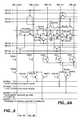
- FIG. 3illustrates an example of the Vt distributions for data stored in an array of memory cells.
- Graph 32shows the Vt distributions for all four data states at the beginning of the cells' life
- graph 34shows the Vt distributions for all four data states at the end of the cells' life.
- the graphsindicate a shift, a decrease, in the Vt distribution for all four data states.
- the Vtdecreases due to loss of stored charge during cell life, which in turn lowers complimentary bit disturb. This complementary bit disturb phenomenon occurs when one side of a memory cell is programmed, wherein the Vt of the other side is increased. The harder one side is programmed, the more the Vt of the other side is increased.
- What is neededis a method for reading a dual bit memory cell that increases the chance of obtaining an accurate data reading throughout memory cell life, particularly at the end of the cell's life. What is also needed is a y-decoder architecture utilizing this more accurate reading method.
- the present inventionis directed at addressing the above-mentioned shortcomings, disadvantages, and problems.
- the present inventionprovides for a method for reading at least one programmed dual bit memory cell using a plurality of programmed dual bit reference cells, each said memory and reference cell comprising a left storage region for storing a first data bit as a level of electron charge and a right storage region for storing a second data bit as a level of electron charge, each said storage region comprising either a low programmed state (a data bit 0) wherein said electron charge is stored in said storage region or a high programmed state (a data bit 1) wherein no said electron charge is stored in said storage region, wherein each said cell has four possible data states 00, 01, 10, and 11, said method comprising.the steps of: (a) programming said reference cells according to a plurality of programming parameters, wherein said first and second data bits of said selected programmed memory cell are determined by reading said first and second data bits of said programmed reference cells; (b) selecting one of the said memory cells to read and determine said
- the methodis implemented using two corresponding reference cells to determine the data stored in one programmed memory cell. In another embodiment of the present invention, the method is implemented using three corresponding reference cells to determine the data stored in one programmed memory cell.
- a key advantage of the method of reading dual-bit memory cells according to the present inventionis more accurate memory cell reading over the life of the memory device.
- the present inventionalso provides for a y-decoder architecture used to read the dual-bit memory cells.
- a y-decoder architectureused to read the dual-bit memory cells.
- One advantageis that it uses less byte select lines as well as byte select transistors as you write. The other is that it requires less program time.
- FIG. 1is a structural illustration of a prior art dual bit memory cell
- FIGS. 2A-2Billustrate a prior y-decoder for reading a dual-bit memory cell
- FIG. 3illustrates an example of the V t distributions for data stored in an array of memory cells
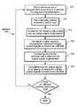
- FIG. 4illustrates a method for reading at least one programmed dual-bit memory cell according to a preferred embodiment of the present invention
- FIG. 5illustrates the programming parameters for Ref 1 , Ref 2 and Ref 3 ;
- FIG. 6illustrate s the programming parameters for Ref 1 and Ref 2 ;
- FIG. 7illustrates the programming parameters for Ref 1 , Ref 2 , and Ref 3 ;
- FIGS. 8A-8Billustrate a y-decoder 50 according to a preferred embodiment of the present invention
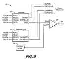
- FIG. 9illustrates block diagram of a circuit 60 used to supply DATABn, DATABn+8, and DATABPqv signals to the y-decoder, and to provide the inputs SAIN and SAREF to sense amplifier 68 , to determine OUT 70 , which determines the data in the memory cell being read;
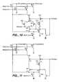
- FIG. 10illustrates Cascode 62 , according to the present invention.
- Cascode 62provides drain voltage for read
- FIG. 11illustrates Cascode_pre 64 , according to the present invention.
- Cascode_pre 64provides the voltage for pre-charge
- FIG. 12illustrates two programming approaches that show one advantage of a y-decoder in accordance with the present invention.
- FIG. 13illustrates a chart comparing the total number of bus lines needed for the present invention and the prior art.
- the present inventionprovides for a method of reading dual-bit memory cells using a plurality of reference cells.
- Each memory cell and reference cellis preferably of the type illustrated in FIG. 1, having a left and right nitride storage region capable of storing a normal and complimentary data bit, respectively.
- storage regions comprised of a nitride layerare preferred, one of ordinary skill in the art will readily realize that the detailed method discussed herein can be modified for implementation with cells comprising storage regions that are floating gates.
- the memory cellsare arranged in an array, to form a memory device.
- One embodiment of this inventionuses two reference cells and another embodiment uses three reference cells
- FIG. 4illustrates a method 100 for reading at least one programmed dual-bit memory cell, according to a preferred embodiment of the present invention.
- each reference cellis programmed according to a plurality of programming parameters.
- the programming parametersare discussed in detail below and depend upon the number of references being programmed for a given memory device.
- the programming technique discussed aboveis preferably used, wherein the gate programming voltage is 9.5 volts, and the drain programming voltage is 5 volts.
- the y-decoderselects a memory cell to read, and reads the cell's normal bit to generate a normal bit output signal, at step 115 .
- This output signalis generally a current that is converted to a voltage.
- the preferred circuits used in programming and reading the memory cellsare illustrated in FIGS. 10-13, and are discussed in detail below.
- the technique for reading a dual-bit cell discussed aboveis preferably used, wherein the gate reading voltage is 4.2 volts, and the drain reading voltage is 1.2 volts.
- the memory cell's normal bit signalis compared to output voltage signals generated by a reference cell cascade circuit, to determine the normal bit cell data.
- the cascade circuit for generating the reference cell output signalis known by those of ordinary skill in the art.
- the selected memory cell's complimentary bit datais read, to generate a complimentary bit output signal.
- the memory cell's complimentary bit output signalis compared to output voltage signals generated by the reference cells, at step 130 , to determine the complimentary bit cell data.
- one embodiment of the present inventionuses two programmed reference cells, Ref 1 and Ref 2 , to determine memory cell data.
- Ref 1 and Ref 2are programmed and their Vt set according to the following programming parameters, to accurately determine the content of memory cells from the beginning to the end of the life of the memory device. These programming parameters are determined based upon the Vt distributions for the memory cell data at the beginning and end of life, as shown in FIGS. 5 and 6, and further illustrated below in Table 1 below:
- the programming parametersimplement the following conditions:
- Vt of Ref 2less than delta Vt between normal and complimentary bits for cell data 01 or 10, i.e. Vt of Ref 2 ⁇ Vt of Ref 1 ⁇ (Vt01 ⁇ Vt10), wherein if normal bit reference data is 01, complimentary bit reference data needs to read 00 for memory cell data 10, and 11 for memory cell data 01.
- Ref 1is set to 2.30 V and Ref 2 is set to 3.45 V.
- Memory cell datacan then be determined by reading the normal and complimentary bits of Ref 1 and Ref 2 , in accordance with Table 3.
- Table 3illustrates one other important parameter, Vt for Ref 1 and Ref 2 cannot be set such that normal bit data for Ref 1 and Ref 2 is 0 and 1 respectively and complimentary bit data for Ref 1 and Ref 2 is 0 and 1 respectively.
- FIGS. 5 and 7illustrate the programming parameters for Ref 1 , Ref 2 and Ref 3 .
- the programming parametersinclude:
- Ref 1 , Ref 2 and Ref 3corresponds to the normal and complimentary bit data for Ref 1 , Ref 3 and Ref 2 , respectively, for each memory cell data state as shown below in Table 4.
- Memory cell datacan then be determined by reading the normal and complimentary bits of corresponding Ref 1 , Ref 2 and Ref 3 , in accordance with Table 5.
- Vt for Ref 1 , Ref 2 and Ref 3cannot be set such that normal bit data for Ref 1 , Ref 3 and Ref 2 is 0,1 and 1 respectively and complimentary bit data for Ref 1 , Ref 3 and Ref 2 is 0, 1 and 1 respectively.
- Vt for Ref 1 , Ref 3 and Ref 2cannot be set such that normal bit data for Ref 1 , Ref 3 and Ref 2 is 0,0 and 1 respectively and complimentary bit data for Ref 1 , Ref 3 and Ref 2 is 0, 0 and 1 respectively.
- FIGS. 8A-8Billustrate a y-decoder 50 according to a preferred embodiment of the present invention for use in programming and reading dual bit cells.
- the y-decoder 50comprises a DATAB(n), e.g. DATAB( 0 ), and a DATAB(n+8), e.g. DATAB( 8 ) for decoding a drain voltage in read for the normal and complimentary data bits.
- DATABnis the drain for programming IOn
- DATABn+8 or DATABn ⁇ 8is the drain for reading IOn.
- the y-decoder 50also comprises a DATABPqv (q being L or H for low or high byte) for decoding a pre-charge voltage in read.
- DATABn and DATABPqvare decoded to read two bits in one cell instead of decoding the byte select, as the prior art y-decoder does.
- two BSDare selected for drain and source.
- Two BSPare selected for pre-charging the bit line next to drain and grounding the bit line next to source. While one of DATABn or DATABPqv is selected, the other DATABn or DATABPqv is grounded.
- FIG. 9illustrates a block diagram of a circuit 60 used to supply DATABn, DATABn+8, and DATABPqv signals to the y-decoder 50 .
- the circuit 60also provides inputs SAIN and SAREF to sense amplifier 68 to determine OUT 70 , which determines the data in the memory cell being read.
- FIG. 10illustrates one embodiment for.Cascode 62 according to the present invention.
- Cascode 62provides drain voltage for read. Memory cell current is transferred to SAIN voltage. When cell current is small (data 0), SAIN is relatively high. When cell current is large (data 1), SAIN is relatively low. SAIN is compared with SAREF, which is cascode output for reference cell to determine a, memory cell data.
- FIG. 11illustrates one embodiment for Cascode_pre 64 according to the present invention.
- Cascode_pre 64provides the voltage for pre-charge.
- first readH
- DATABPEvis 1.2 v while the DATABPOv is grounded.
- second readH
- DATABPEvis grounded while the DATABPOv is 1.2 v.
- FIG. 12illustrates two programming approaches.
- Approach 1is for the y-decoder according to the present invention.
- Approach 2is for the prior art y-decoder.
- Approach 1does not need discharge time between the two sub-programs, while Approach 2 needs the discharge time. For example, assuming a pump time of. 160 ns for Vcc to 6 volts, and 480 ns for 6 volts to 9.5 volts, the result is an extra 640 ns as shown.
- FIG. 13illustrates a chart comparing the total number of bus lines needed for the present invention and the prior art.
- the figureillustrates that fewer bus lines and fewer byte selects are required in the y-decoder of the present invention. For instance, when putting two bits in one IO, one IO has 64 diffusion bit lines (cells) and 128 bits. For putting 2 bits per cell in different IOs, two IOs are combined together, so that one IO block, which is made of two IOs, has 128 diffusion bit lines and 256 bits.
- the prior art y-decoderrequires doubling both column select and byte select.
Landscapes
- Engineering & Computer Science (AREA)
- Microelectronics & Electronic Packaging (AREA)
- Read Only Memory (AREA)
- Semiconductor Memories (AREA)
- Non-Volatile Memory (AREA)
Abstract
Description
| TABLE 1 | ||
| Beginning of life | End of Life | |
| Data | (BOL) | (EOL) |
| 11 | Max. | 1.7v | Max. | 1.5 | |
| 10 | Max. | 3.2v | Max. | 2.2v | |
| 01 | Min. | 4.2v | Min. | 2.9v | |
| 00 | Min. | 4.2v | Min. | 3.4v | |
| TABLE 2 | ||
| Memory Cell Data | Normal Bit Data | |
| 1, 1 | 1, 1 | 1, 1 |
| 1, 0 | 1, 1 or 0, 1 | 0, 1 or 0, 0 |
| 0, 1 | 0, 1 or 0, 0 | 1, 1 or 0, 1 |
| 0, 0 | 0, 0 | 0, 0 |
| TABLE 3 | |||
| Normal Bit | Complimentary Bit | ||
| Ref1 | Ref2 | Ref1 | Cell Data | ||
| 1 | 1 | 1 | 1 | 1, 1 | |
| 1 | 1 | 0 | 1 | 1, 0 | |
| 1 | 1 | 0 | 0 | 1, 0 | |
| 0 | 1 | 1 | 1 | 0, 1 | |
| 0 | 1 | 0 | 1 | N/ | |
| 0 | 1 | 0 | 0 | 1, 0 | |
| 0 | 0 | 1 | 1 | 0, 1 | |
| 0 | 0 | 0 | 1 | 0, 1 | |
| 0 | 0 | 0 | 0 | 0, 0 | |
| TABLE 4 | ||||
| Memory | Normal | Complimentary | ||
| Cell Data | Bit | Bit Data | ||
| 1, 1 | 1, 1, 1 | 1, 1, 1 | ||
| 1, 0 | 1, 1, 1 or | 0, 1, 1 or | ||
| 0, 1, 1 or | 0, 0, 1 or | |||
| 0, 0, 1 | 0, 0, 0 | |||
| 0, 1 | 0, 1, 1 or | 1, 1, 1 or | ||
| 0, 0, 1 or | 0, 1, 1 or | |||
| 0, 0, 0 | 0, 0, 1 | |||
| 0, 0 | 0, 0, 0 | 0, 0, 0 | ||
| TABLE 5 | ||
| Normal Bit | Complimentary Bit | Cell |
| Ref1 | Ref3 | Ref2 | Ref1 | Ref2 | Data | ||
| 1 | 1 | 1 | 1 | 1 | 1 | 1, 1 | |
| 1 | 1 | 1 | 0 | 1 | 1 | 1, 0 | |
| 1 | 1 | 1 | 0 | 0 | 1 | 1, 0 | |
| 1 | 1 | 1 | 0 | 0 | 0 | 1, 0 | |
| 0 | 1 | 1 | 1 | 1 | 1 | 0, 1 | |
| 0 | 1 | 1 | 0 | 1 | 1 | N/ | |
| 0 | 1 | 1 | 0 | 0 | 1 | 1, 0 | |
| 0 | 1 | 1 | 0 | 0 | 0 | 1, 0 | |
| 0 | 0 | 1 | 1 | 1 | 1 | 0, 1 | |
| 0 | 0 | 1 | 0 | 1 | 1 | 0, 1 | |
| 0 | 0 | 1 | 0 | 0 | 1 | N/ | |
| 0 | 0 | 1 | 0 | 0 | 0 | 1, 0 | |
| 0 | 0 | 0 | 1 | 1 | 1 | 0, 1 | |
| 0 | 0 | 0 | 0 | 1 | 1 | 0, 1 | |
| 0 | 0 | 0 | 0 | 0 | 1 | 0, 1 | |
| 0 | 0 | 0 | 0 | 0 | 0 | 0, 0 | |
Claims (12)
Priority Applications (4)
| Application Number | Priority Date | Filing Date | Title |
|---|---|---|---|
| US10/052,484US6574139B2 (en) | 2001-06-20 | 2002-01-18 | Method and device for reading dual bit memory cells using multiple reference cells with two side read |
| EP02252915AEP1271550B1 (en) | 2001-06-20 | 2002-04-25 | Method and device for reading dual bit memory cells using multiple reference cells with two side read |
| DE60216010TDE60216010T2 (en) | 2001-06-20 | 2002-04-25 | Method and circuit for reading out double-bit memory cells using a plurality of double-bit reference memory cells that are read both-way |
| JP2002177482AJP4142354B2 (en) | 2001-06-20 | 2002-06-18 | Dual bit memory cell reading method and apparatus |
Applications Claiming Priority (2)
| Application Number | Priority Date | Filing Date | Title |
|---|---|---|---|
| US30091601P | 2001-06-20 | 2001-06-20 | |
| US10/052,484US6574139B2 (en) | 2001-06-20 | 2002-01-18 | Method and device for reading dual bit memory cells using multiple reference cells with two side read |
Publications (2)
| Publication Number | Publication Date |
|---|---|
| US20030081458A1 US20030081458A1 (en) | 2003-05-01 |
| US6574139B2true US6574139B2 (en) | 2003-06-03 |
Family
ID=26730664
Family Applications (1)
| Application Number | Title | Priority Date | Filing Date |
|---|---|---|---|
| US10/052,484Expired - LifetimeUS6574139B2 (en) | 2001-06-20 | 2002-01-18 | Method and device for reading dual bit memory cells using multiple reference cells with two side read |
Country Status (4)
| Country | Link |
|---|---|
| US (1) | US6574139B2 (en) |
| EP (1) | EP1271550B1 (en) |
| JP (1) | JP4142354B2 (en) |
| DE (1) | DE60216010T2 (en) |
Cited By (36)
| Publication number | Priority date | Publication date | Assignee | Title |
|---|---|---|---|---|
| US20040153620A1 (en)* | 2003-01-30 | 2004-08-05 | Shai Eisen | Address scramble |
| US6775187B1 (en)* | 2003-04-24 | 2004-08-10 | Advanced Micro Devices, Inc. | Method of programming a dual cell memory device |
| US20040218426A1 (en)* | 2003-04-29 | 2004-11-04 | Oleg Dadashev | Apparatus and methods for multi-level sensing in a memory array |
| US6917544B2 (en) | 2002-07-10 | 2005-07-12 | Saifun Semiconductors Ltd. | Multiple use memory chip |
| US20050232024A1 (en)* | 2004-04-19 | 2005-10-20 | Shahar Atir | Method for reading a memory array with neighbor effect cancellation |
| US6963505B2 (en) | 2002-10-29 | 2005-11-08 | Aifun Semiconductors Ltd. | Method circuit and system for determining a reference voltage |
| US6992932B2 (en) | 2002-10-29 | 2006-01-31 | Saifun Semiconductors Ltd | Method circuit and system for read error detection in a non-volatile memory array |
| US20060034122A1 (en)* | 2004-08-12 | 2006-02-16 | Yoram Betser | Dynamic matching of signal path and reference path for sensing |
| US7064983B2 (en) | 2001-04-05 | 2006-06-20 | Saifum Semiconductors Ltd. | Method for programming a reference cell |
| US7184313B2 (en) | 2005-06-17 | 2007-02-27 | Saifun Semiconductors Ltd. | Method circuit and system for compensating for temperature induced margin loss in non-volatile memory cells |
| US20070058443A1 (en)* | 2004-03-05 | 2007-03-15 | Joachim Deppe | Method for operating an electrical writable and erasable memory cell and a memory device for electrical memories |
| US7221138B2 (en) | 2005-09-27 | 2007-05-22 | Saifun Semiconductors Ltd | Method and apparatus for measuring charge pump output current |
| US7257025B2 (en) | 2004-12-09 | 2007-08-14 | Saifun Semiconductors Ltd | Method for reading non-volatile memory cells |
| US7317633B2 (en) | 2004-07-06 | 2008-01-08 | Saifun Semiconductors Ltd | Protection of NROM devices from charge damage |
| US7352627B2 (en) | 2006-01-03 | 2008-04-01 | Saifon Semiconductors Ltd. | Method, system, and circuit for operating a non-volatile memory array |
| US7369440B2 (en) | 2005-01-19 | 2008-05-06 | Saifun Semiconductors Ltd. | Method, circuit and systems for erasing one or more non-volatile memory cells |
| US7405969B2 (en) | 1997-08-01 | 2008-07-29 | Saifun Semiconductors Ltd. | Non-volatile memory cell and non-volatile memory devices |
| US7420848B2 (en) | 2002-01-31 | 2008-09-02 | Saifun Semiconductors Ltd. | Method, system, and circuit for operating a non-volatile memory array |
| US7457183B2 (en) | 2003-09-16 | 2008-11-25 | Saifun Semiconductors Ltd. | Operating array cells with matched reference cells |
| US7535765B2 (en) | 2004-12-09 | 2009-05-19 | Saifun Semiconductors Ltd. | Non-volatile memory device and method for reading cells |
| US7590001B2 (en) | 2007-12-18 | 2009-09-15 | Saifun Semiconductors Ltd. | Flash memory with optimized write sector spares |
| US7605579B2 (en) | 2006-09-18 | 2009-10-20 | Saifun Semiconductors Ltd. | Measuring and controlling current consumption and output current of charge pumps |
| US7638850B2 (en) | 2004-10-14 | 2009-12-29 | Saifun Semiconductors Ltd. | Non-volatile memory structure and method of fabrication |
| US7638835B2 (en) | 2006-02-28 | 2009-12-29 | Saifun Semiconductors Ltd. | Double density NROM with nitride strips (DDNS) |
| US7652930B2 (en) | 2004-04-01 | 2010-01-26 | Saifun Semiconductors Ltd. | Method, circuit and system for erasing one or more non-volatile memory cells |
| US7668017B2 (en) | 2005-08-17 | 2010-02-23 | Saifun Semiconductors Ltd. | Method of erasing non-volatile memory cells |
| US7675782B2 (en) | 2002-10-29 | 2010-03-09 | Saifun Semiconductors Ltd. | Method, system and circuit for programming a non-volatile memory array |
| US7692961B2 (en) | 2006-02-21 | 2010-04-06 | Saifun Semiconductors Ltd. | Method, circuit and device for disturb-control of programming nonvolatile memory cells by hot-hole injection (HHI) and by channel hot-electron (CHE) injection |
| US7701779B2 (en) | 2006-04-27 | 2010-04-20 | Sajfun Semiconductors Ltd. | Method for programming a reference cell |
| US7743230B2 (en) | 2003-01-31 | 2010-06-22 | Saifun Semiconductors Ltd. | Memory array programming circuit and a method for using the circuit |
| US7760554B2 (en) | 2006-02-21 | 2010-07-20 | Saifun Semiconductors Ltd. | NROM non-volatile memory and mode of operation |
| US7786512B2 (en) | 2005-07-18 | 2010-08-31 | Saifun Semiconductors Ltd. | Dense non-volatile memory array and method of fabrication |
| US7808818B2 (en) | 2006-01-12 | 2010-10-05 | Saifun Semiconductors Ltd. | Secondary injection for NROM |
| US8053812B2 (en) | 2005-03-17 | 2011-11-08 | Spansion Israel Ltd | Contact in planar NROM technology |
| US8253452B2 (en) | 2006-02-21 | 2012-08-28 | Spansion Israel Ltd | Circuit and method for powering up an integrated circuit and an integrated circuit utilizing same |
| US8400841B2 (en) | 2005-06-15 | 2013-03-19 | Spansion Israel Ltd. | Device to program adjacent storage cells of different NROM cells |
Families Citing this family (7)
| Publication number | Priority date | Publication date | Assignee | Title |
|---|---|---|---|---|
| US6690602B1 (en) | 2002-04-08 | 2004-02-10 | Advanced Micro Devices, Inc. | Algorithm dynamic reference programming |
| US6956768B2 (en)* | 2003-04-15 | 2005-10-18 | Advanced Micro Devices, Inc. | Method of programming dual cell memory device to store multiple data states per cell |
| US7324374B2 (en)* | 2003-06-20 | 2008-01-29 | Spansion Llc | Memory with a core-based virtual ground and dynamic reference sensing scheme |
| JP2007109360A (en)* | 2005-09-15 | 2007-04-26 | Sharp Corp | Semiconductor memory device reading method and semiconductor memory device |
| JP4523531B2 (en)* | 2005-09-29 | 2010-08-11 | シャープ株式会社 | Semiconductor memory device, reading method thereof, and electronic apparatus |
| US9715430B2 (en)* | 2015-07-01 | 2017-07-25 | Nandext Srl | Controller for a solid-state drive, and related solid-state drive |
| US12436887B1 (en)* | 2024-03-26 | 2025-10-07 | Advanced Micro Devices, Inc. | Data-driven precision for memory access |
Citations (3)
| Publication number | Priority date | Publication date | Assignee | Title |
|---|---|---|---|---|
| US5414693A (en)* | 1991-08-29 | 1995-05-09 | Hyundai Electronics Industries Co., Ltd. | Self-aligned dual-bit split gate (DSG) flash EEPROM cell |
| US5949711A (en)* | 1996-09-26 | 1999-09-07 | Waferscale Integration, Inc. | Dual bit memory cell |
| US6438031B1 (en)* | 2000-02-16 | 2002-08-20 | Advanced Micro Devices, Inc. | Method of programming a non-volatile memory cell using a substrate bias |
Family Cites Families (5)
| Publication number | Priority date | Publication date | Assignee | Title |
|---|---|---|---|---|
| JPH07120720B2 (en)* | 1987-12-17 | 1995-12-20 | 三菱電機株式会社 | Nonvolatile semiconductor memory device |
| US5172338B1 (en)* | 1989-04-13 | 1997-07-08 | Sandisk Corp | Multi-state eeprom read and write circuits and techniques |
| DE69702256T2 (en)* | 1996-06-24 | 2001-01-18 | Advanced Micro Devices, Inc. | METHOD FOR A MULTIPLE, BITS PER CELL FLASH EEPROM, MEMORY WITH SIDE PROGRAMMING MODE, AND READING METHOD |
| US6768165B1 (en)* | 1997-08-01 | 2004-07-27 | Saifun Semiconductors Ltd. | Two bit non-volatile electrically erasable and programmable semiconductor memory cell utilizing asymmetrical charge trapping |
| US6215697B1 (en)* | 1999-01-14 | 2001-04-10 | Macronix International Co., Ltd. | Multi-level memory cell device and method for self-converged programming |
- 2002
- 2002-01-18USUS10/052,484patent/US6574139B2/ennot_activeExpired - Lifetime
- 2002-04-25EPEP02252915Apatent/EP1271550B1/ennot_activeExpired - Lifetime
- 2002-04-25DEDE60216010Tpatent/DE60216010T2/ennot_activeExpired - Lifetime
- 2002-06-18JPJP2002177482Apatent/JP4142354B2/ennot_activeExpired - Fee Related
Patent Citations (3)
| Publication number | Priority date | Publication date | Assignee | Title |
|---|---|---|---|---|
| US5414693A (en)* | 1991-08-29 | 1995-05-09 | Hyundai Electronics Industries Co., Ltd. | Self-aligned dual-bit split gate (DSG) flash EEPROM cell |
| US5949711A (en)* | 1996-09-26 | 1999-09-07 | Waferscale Integration, Inc. | Dual bit memory cell |
| US6438031B1 (en)* | 2000-02-16 | 2002-08-20 | Advanced Micro Devices, Inc. | Method of programming a non-volatile memory cell using a substrate bias |
Cited By (46)
| Publication number | Priority date | Publication date | Assignee | Title |
|---|---|---|---|---|
| US7405969B2 (en) | 1997-08-01 | 2008-07-29 | Saifun Semiconductors Ltd. | Non-volatile memory cell and non-volatile memory devices |
| US7064983B2 (en) | 2001-04-05 | 2006-06-20 | Saifum Semiconductors Ltd. | Method for programming a reference cell |
| US7420848B2 (en) | 2002-01-31 | 2008-09-02 | Saifun Semiconductors Ltd. | Method, system, and circuit for operating a non-volatile memory array |
| US6917544B2 (en) | 2002-07-10 | 2005-07-12 | Saifun Semiconductors Ltd. | Multiple use memory chip |
| US7738304B2 (en) | 2002-07-10 | 2010-06-15 | Saifun Semiconductors Ltd. | Multiple use memory chip |
| US6963505B2 (en) | 2002-10-29 | 2005-11-08 | Aifun Semiconductors Ltd. | Method circuit and system for determining a reference voltage |
| US6992932B2 (en) | 2002-10-29 | 2006-01-31 | Saifun Semiconductors Ltd | Method circuit and system for read error detection in a non-volatile memory array |
| US7675782B2 (en) | 2002-10-29 | 2010-03-09 | Saifun Semiconductors Ltd. | Method, system and circuit for programming a non-volatile memory array |
| US6967896B2 (en) | 2003-01-30 | 2005-11-22 | Saifun Semiconductors Ltd | Address scramble |
| US20040153620A1 (en)* | 2003-01-30 | 2004-08-05 | Shai Eisen | Address scramble |
| US7743230B2 (en) | 2003-01-31 | 2010-06-22 | Saifun Semiconductors Ltd. | Memory array programming circuit and a method for using the circuit |
| US6775187B1 (en)* | 2003-04-24 | 2004-08-10 | Advanced Micro Devices, Inc. | Method of programming a dual cell memory device |
| US7142464B2 (en) | 2003-04-29 | 2006-11-28 | Saifun Semiconductors Ltd. | Apparatus and methods for multi-level sensing in a memory array |
| US20040218426A1 (en)* | 2003-04-29 | 2004-11-04 | Oleg Dadashev | Apparatus and methods for multi-level sensing in a memory array |
| US7457183B2 (en) | 2003-09-16 | 2008-11-25 | Saifun Semiconductors Ltd. | Operating array cells with matched reference cells |
| US7411837B2 (en)* | 2004-03-05 | 2008-08-12 | Infineon Technologies Ag | Method for operating an electrical writable and erasable memory cell and a memory device for electrical memories |
| US20070058443A1 (en)* | 2004-03-05 | 2007-03-15 | Joachim Deppe | Method for operating an electrical writable and erasable memory cell and a memory device for electrical memories |
| US7532529B2 (en) | 2004-03-29 | 2009-05-12 | Saifun Semiconductors Ltd. | Apparatus and methods for multi-level sensing in a memory array |
| US7652930B2 (en) | 2004-04-01 | 2010-01-26 | Saifun Semiconductors Ltd. | Method, circuit and system for erasing one or more non-volatile memory cells |
| US7755938B2 (en) | 2004-04-19 | 2010-07-13 | Saifun Semiconductors Ltd. | Method for reading a memory array with neighbor effect cancellation |
| US20050232024A1 (en)* | 2004-04-19 | 2005-10-20 | Shahar Atir | Method for reading a memory array with neighbor effect cancellation |
| US7317633B2 (en) | 2004-07-06 | 2008-01-08 | Saifun Semiconductors Ltd | Protection of NROM devices from charge damage |
| US7095655B2 (en) | 2004-08-12 | 2006-08-22 | Saifun Semiconductors Ltd. | Dynamic matching of signal path and reference path for sensing |
| US7466594B2 (en) | 2004-08-12 | 2008-12-16 | Saifun Semiconductors Ltd. | Dynamic matching of signal path and reference path for sensing |
| US20060034122A1 (en)* | 2004-08-12 | 2006-02-16 | Yoram Betser | Dynamic matching of signal path and reference path for sensing |
| US7638850B2 (en) | 2004-10-14 | 2009-12-29 | Saifun Semiconductors Ltd. | Non-volatile memory structure and method of fabrication |
| US7964459B2 (en) | 2004-10-14 | 2011-06-21 | Spansion Israel Ltd. | Non-volatile memory structure and method of fabrication |
| US7535765B2 (en) | 2004-12-09 | 2009-05-19 | Saifun Semiconductors Ltd. | Non-volatile memory device and method for reading cells |
| US7257025B2 (en) | 2004-12-09 | 2007-08-14 | Saifun Semiconductors Ltd | Method for reading non-volatile memory cells |
| US7369440B2 (en) | 2005-01-19 | 2008-05-06 | Saifun Semiconductors Ltd. | Method, circuit and systems for erasing one or more non-volatile memory cells |
| US7468926B2 (en) | 2005-01-19 | 2008-12-23 | Saifun Semiconductors Ltd. | Partial erase verify |
| US8053812B2 (en) | 2005-03-17 | 2011-11-08 | Spansion Israel Ltd | Contact in planar NROM technology |
| US8400841B2 (en) | 2005-06-15 | 2013-03-19 | Spansion Israel Ltd. | Device to program adjacent storage cells of different NROM cells |
| US7184313B2 (en) | 2005-06-17 | 2007-02-27 | Saifun Semiconductors Ltd. | Method circuit and system for compensating for temperature induced margin loss in non-volatile memory cells |
| US7786512B2 (en) | 2005-07-18 | 2010-08-31 | Saifun Semiconductors Ltd. | Dense non-volatile memory array and method of fabrication |
| US7668017B2 (en) | 2005-08-17 | 2010-02-23 | Saifun Semiconductors Ltd. | Method of erasing non-volatile memory cells |
| US7221138B2 (en) | 2005-09-27 | 2007-05-22 | Saifun Semiconductors Ltd | Method and apparatus for measuring charge pump output current |
| US7352627B2 (en) | 2006-01-03 | 2008-04-01 | Saifon Semiconductors Ltd. | Method, system, and circuit for operating a non-volatile memory array |
| US7808818B2 (en) | 2006-01-12 | 2010-10-05 | Saifun Semiconductors Ltd. | Secondary injection for NROM |
| US7760554B2 (en) | 2006-02-21 | 2010-07-20 | Saifun Semiconductors Ltd. | NROM non-volatile memory and mode of operation |
| US7692961B2 (en) | 2006-02-21 | 2010-04-06 | Saifun Semiconductors Ltd. | Method, circuit and device for disturb-control of programming nonvolatile memory cells by hot-hole injection (HHI) and by channel hot-electron (CHE) injection |
| US8253452B2 (en) | 2006-02-21 | 2012-08-28 | Spansion Israel Ltd | Circuit and method for powering up an integrated circuit and an integrated circuit utilizing same |
| US7638835B2 (en) | 2006-02-28 | 2009-12-29 | Saifun Semiconductors Ltd. | Double density NROM with nitride strips (DDNS) |
| US7701779B2 (en) | 2006-04-27 | 2010-04-20 | Sajfun Semiconductors Ltd. | Method for programming a reference cell |
| US7605579B2 (en) | 2006-09-18 | 2009-10-20 | Saifun Semiconductors Ltd. | Measuring and controlling current consumption and output current of charge pumps |
| US7590001B2 (en) | 2007-12-18 | 2009-09-15 | Saifun Semiconductors Ltd. | Flash memory with optimized write sector spares |
Also Published As
| Publication number | Publication date |
|---|---|
| JP4142354B2 (en) | 2008-09-03 |
| EP1271550A3 (en) | 2004-06-23 |
| EP1271550A2 (en) | 2003-01-02 |
| DE60216010T2 (en) | 2007-05-24 |
| JP2003068087A (en) | 2003-03-07 |
| EP1271550B1 (en) | 2006-11-15 |
| DE60216010D1 (en) | 2006-12-28 |
| US20030081458A1 (en) | 2003-05-01 |
Similar Documents
| Publication | Publication Date | Title |
|---|---|---|
| US6574139B2 (en) | Method and device for reading dual bit memory cells using multiple reference cells with two side read | |
| US6058060A (en) | Multi-bit-per-cell and analog/multi-level non-volatile memories with improved resolution and signal-to noise ratio | |
| US7489544B2 (en) | Flash memory device having multi-level cell and reading and programming method thereof | |
| US8325542B2 (en) | Complementary reference method for high reliability trap-type non-volatile memory | |
| US6525960B2 (en) | Nonvolatile semiconductor memory device including correction of erratic memory cell data | |
| US6181599B1 (en) | Method for applying variable row BIAS to reduce program disturb in a flash memory storage array | |
| EP0477369B1 (en) | Semiconductor memory device | |
| JP4084922B2 (en) | Non-volatile memory device writing method | |
| US6122198A (en) | Bit by bit APDE verify for flash memory applications | |
| US8085607B2 (en) | 3-level non-volatile semiconductor memory device and method of driving the same | |
| US6621745B1 (en) | Row decoder circuit for use in programming a memory device | |
| US7167395B1 (en) | Non-volatile semiconductor memory | |
| JPH1011981A (en) | Non-volatile semiconductor storage device | |
| US6661709B2 (en) | Nonvolatile semiconductor memory device | |
| US6320785B1 (en) | Nonvolatile semiconductor memory device and data writing method therefor | |
| US5025417A (en) | Semiconductor memory device capable of preventing data of non-selected memory cell from being degraded | |
| US20040156239A1 (en) | Nonvolatile semiconductor memory device | |
| US6567314B1 (en) | Data programming implementation for high efficiency CHE injection | |
| KR100413997B1 (en) | Nonvolatile semiconductor memory | |
| US5903497A (en) | Integrated program verify page buffer | |
| JP3417817B2 (en) | Non-volatile semiconductor memory | |
| JPH113597A (en) | Nonvolatile semiconductor memory device, method of verifying write data of nonvolatile semiconductor memory device, and method of writing data of nonvolatile semiconductor memory device |
Legal Events
| Date | Code | Title | Description |
|---|---|---|---|
| AS | Assignment | Owner name:FUJITSU LIMITED, JAPAN Free format text:ASSIGNMENT OF ASSIGNORS INTEREST;ASSIGNOR:KURIHARA, KAZUHIRO;REEL/FRAME:012938/0735 Effective date:20020419 | |
| STCF | Information on status: patent grant | Free format text:PATENTED CASE | |
| FEPP | Fee payment procedure | Free format text:PAYER NUMBER DE-ASSIGNED (ORIGINAL EVENT CODE: RMPN); ENTITY STATUS OF PATENT OWNER: LARGE ENTITY Free format text:PAYOR NUMBER ASSIGNED (ORIGINAL EVENT CODE: ASPN); ENTITY STATUS OF PATENT OWNER: LARGE ENTITY | |
| FPAY | Fee payment | Year of fee payment:4 | |
| AS | Assignment | Owner name:SPANSION INC.,CALIFORNIA Free format text:ASSIGNMENT OF ASSIGNORS INTEREST;ASSIGNOR:FUJITSU LIMITED;REEL/FRAME:024225/0119 Effective date:20051221 | |
| AS | Assignment | Owner name:BARCLAYS BANK PLC,NEW YORK Free format text:SECURITY AGREEMENT;ASSIGNORS:SPANSION LLC;SPANSION INC.;SPANSION TECHNOLOGY INC.;AND OTHERS;REEL/FRAME:024522/0338 Effective date:20100510 Owner name:BARCLAYS BANK PLC, NEW YORK Free format text:SECURITY AGREEMENT;ASSIGNORS:SPANSION LLC;SPANSION INC.;SPANSION TECHNOLOGY INC.;AND OTHERS;REEL/FRAME:024522/0338 Effective date:20100510 | |
| FPAY | Fee payment | Year of fee payment:8 | |
| AS | Assignment | Owner name:SPANSION LLC, CALIFORNIA Free format text:ASSIGNMENT OF ASSIGNORS INTEREST;ASSIGNOR:SPANSION INC.;REEL/FRAME:029112/0198 Effective date:20121010 | |
| REMI | Maintenance fee reminder mailed | ||
| AS | Assignment | Owner name:SPANSION INC., CALIFORNIA Free format text:RELEASE BY SECURED PARTY;ASSIGNOR:BARCLAYS BANK PLC;REEL/FRAME:035201/0159 Effective date:20150312 Owner name:SPANSION TECHNOLOGY LLC, CALIFORNIA Free format text:RELEASE BY SECURED PARTY;ASSIGNOR:BARCLAYS BANK PLC;REEL/FRAME:035201/0159 Effective date:20150312 Owner name:SPANSION LLC, CALIFORNIA Free format text:RELEASE BY SECURED PARTY;ASSIGNOR:BARCLAYS BANK PLC;REEL/FRAME:035201/0159 Effective date:20150312 | |
| FPAY | Fee payment | Year of fee payment:12 | |
| SULP | Surcharge for late payment | Year of fee payment:11 | |
| AS | Assignment | Owner name:CYPRESS SEMICONDUCTOR CORPORATION, CALIFORNIA Free format text:ASSIGNMENT OF ASSIGNORS INTEREST;ASSIGNOR:SPANSION, LLC;REEL/FRAME:036034/0230 Effective date:20150601 | |
| AS | Assignment | Owner name:MORGAN STANLEY SENIOR FUNDING, INC., NEW YORK Free format text:SECURITY INTEREST;ASSIGNOR:CYPRESS SEMICONDUCTOR CORPORATION;REEL/FRAME:039676/0237 Effective date:20160805 | |
| AS | Assignment | Owner name:MORGAN STANLEY SENIOR FUNDING, NEW YORK Free format text:CORRECTIVE ASSIGNMENT TO CORRECT THE FOLLOWING NUMBERS 6272046,7277824,7282374,7286384,7299106,7337032,7460920,7519447 PREVIOUSLY RECORDED ON REEL 039676 FRAME 0237. ASSIGNOR(S) HEREBY CONFIRMS THE SECURITY INTEREST;ASSIGNOR:CYPRESS SEMICONDUCTOR CORPORATION;REEL/FRAME:047797/0854 Effective date:20171229 | |
| AS | Assignment | Owner name:MUFG UNION BANK, N.A., CALIFORNIA Free format text:ASSIGNMENT AND ASSUMPTION OF SECURITY INTEREST;ASSIGNOR:MORGAN STANLEY SENIOR FUNDING, INC.;REEL/FRAME:051209/0721 Effective date:20191204 | |
| AS | Assignment | Owner name:SPANSION LLC, CALIFORNIA Free format text:RELEASE BY SECURED PARTY;ASSIGNOR:MUFG UNION BANK, N.A.;REEL/FRAME:059410/0438 Effective date:20200416 Owner name:CYPRESS SEMICONDUCTOR CORPORATION, CALIFORNIA Free format text:RELEASE BY SECURED PARTY;ASSIGNOR:MUFG UNION BANK, N.A.;REEL/FRAME:059410/0438 Effective date:20200416 |