US6570784B2 - Programming a phase-change material memory - Google Patents
Programming a phase-change material memoryDownload PDFInfo
- Publication number
- US6570784B2 US6570784B2US09/895,135US89513501AUS6570784B2US 6570784 B2US6570784 B2US 6570784B2US 89513501 AUS89513501 AUS 89513501AUS 6570784 B2US6570784 B2US 6570784B2
- Authority
- US
- United States
- Prior art keywords
- signal
- memory material
- state
- memory
- fall time
- Prior art date
- Legal status (The legal status is an assumption and is not a legal conclusion. Google has not performed a legal analysis and makes no representation as to the accuracy of the status listed.)
- Expired - Lifetime
Links
- 239000012782phase change materialSubstances0.000titleclaimsabstractdescription39
- 230000015654memoryEffects0.000titleclaimsdescription147
- 239000000463materialSubstances0.000claimsabstractdescription118
- 230000008859changeEffects0.000claimsabstractdescription8
- 238000000034methodMethods0.000claimsdescription68
- 238000002425crystallisationMethods0.000claimsdescription11
- 230000008025crystallizationEffects0.000claimsdescription11
- 238000004519manufacturing processMethods0.000claimsdescription10
- 230000008569processEffects0.000claimsdescription10
- 238000007493shaping processMethods0.000claimsdescription5
- 239000000470constituentSubstances0.000abstractdescription7
- 150000004770chalcogenidesChemical class0.000abstractdescription6
- 239000000956alloySubstances0.000abstractdescription5
- 229910045601alloyInorganic materials0.000abstractdescription5
- 239000004020conductorSubstances0.000description5
- 230000008901benefitEffects0.000description4
- 238000010586diagramMethods0.000description4
- 239000007787solidSubstances0.000description4
- 230000006870functionEffects0.000description3
- 230000005540biological transmissionEffects0.000description2
- 238000004891communicationMethods0.000description2
- 230000001413cellular effectEffects0.000description1
- 238000007796conventional methodMethods0.000description1
- 238000013500data storageMethods0.000description1
- 230000007423decreaseEffects0.000description1
- 230000000694effectsEffects0.000description1
- 230000001747exhibiting effectEffects0.000description1
- 230000010354integrationEffects0.000description1
- 230000007246mechanismEffects0.000description1
- 229910044991metal oxideInorganic materials0.000description1
- 150000004706metal oxidesChemical class0.000description1
- 238000012986modificationMethods0.000description1
- 230000004048modificationEffects0.000description1
- 230000002093peripheral effectEffects0.000description1
- 230000002441reversible effectEffects0.000description1
- 239000004065semiconductorSubstances0.000description1
- 238000012358sourcingMethods0.000description1
- 238000012360testing methodMethods0.000description1
- 230000007704transitionEffects0.000description1
Images


Classifications
- G—PHYSICS
- G11—INFORMATION STORAGE
- G11C—STATIC STORES
- G11C13/00—Digital stores characterised by the use of storage elements not covered by groups G11C11/00, G11C23/00, or G11C25/00
- G11C13/0002—Digital stores characterised by the use of storage elements not covered by groups G11C11/00, G11C23/00, or G11C25/00 using resistive RAM [RRAM] elements
- G11C13/0021—Auxiliary circuits
- G11C13/0069—Writing or programming circuits or methods
- G—PHYSICS
- G11—INFORMATION STORAGE
- G11C—STATIC STORES
- G11C11/00—Digital stores characterised by the use of particular electric or magnetic storage elements; Storage elements therefor
- G11C11/56—Digital stores characterised by the use of particular electric or magnetic storage elements; Storage elements therefor using storage elements with more than two stable states represented by steps, e.g. of voltage, current, phase, frequency
- G11C11/5678—Digital stores characterised by the use of particular electric or magnetic storage elements; Storage elements therefor using storage elements with more than two stable states represented by steps, e.g. of voltage, current, phase, frequency using amorphous/crystalline phase transition storage elements
- G—PHYSICS
- G11—INFORMATION STORAGE
- G11C—STATIC STORES
- G11C13/00—Digital stores characterised by the use of storage elements not covered by groups G11C11/00, G11C23/00, or G11C25/00
- G11C13/0002—Digital stores characterised by the use of storage elements not covered by groups G11C11/00, G11C23/00, or G11C25/00 using resistive RAM [RRAM] elements
- G11C13/0004—Digital stores characterised by the use of storage elements not covered by groups G11C11/00, G11C23/00, or G11C25/00 using resistive RAM [RRAM] elements comprising amorphous/crystalline phase transition cells
- G—PHYSICS
- G11—INFORMATION STORAGE
- G11C—STATIC STORES
- G11C13/00—Digital stores characterised by the use of storage elements not covered by groups G11C11/00, G11C23/00, or G11C25/00
- G11C13/0002—Digital stores characterised by the use of storage elements not covered by groups G11C11/00, G11C23/00, or G11C25/00 using resistive RAM [RRAM] elements
- G11C13/0021—Auxiliary circuits
- G11C13/0069—Writing or programming circuits or methods
- G11C2013/0092—Write characterized by the shape, e.g. form, length, amplitude of the write pulse
Definitions
- This inventionis related to techniques for programming a structural phase-change material solid state memory device such as those that use a chalcogenide material which can be programmed into different resistivity states to store data.
- phase-change memoriesSolid state memory devices that use a structural phase-change material as the data storage mechanism (referred to here simply as ‘phase-change memories’) offer significant advantages in both cost and performance over conventional charge storage based memories.
- the phase-change memoryis made of an array of constituent cells where each cell has some structural phase-change material to store the cell's data.
- This materialmay be, for instance, a chalcogenide alloy that exhibits a reversible structural phase change from amorphous to crystalline.
- a small volume of the chalcogenide alloyis integrated into a circuit that allows the cell to act as a fast switching programmable resistor.
- This programmable resistorcan exhibit greater than 40 times dynamic range of resistivity between the crystalline state (low resistivity) and the amorphous state (high resistivity), and is also capable of exhibiting multiple, intermediate states that allow multi-bit storage in each cell.
- the data stored in the cellis read by measuring the cell's resistance.
- the chalcogenide alloy cellis also non-volatile.
- a conventional technique for programming a phase-change memory cellis to apply a rectangular pulse of current (having a constant magnitude) to the cell, at a voltage greater than a switching threshold for the phase-change material, which leaves the material in the reset state (amorphous and high resistivity). This may be followed by the application of a subsequent rectangular pulse, also at a voltage greater than the switching threshold, which changes the material to a set state (crystalline and low resistivity).
- the reset pulsehas a higher magnitude of current than the set pulse so that the temperature of the phase change material is raised to T m , the amorphizing temperature, before the material is rapidly cooled down and is left in the amorphous state.
- the materialcan be heated back up to an optimum temperature T opt , which is lower than T m .
- T optis that which allows the material in the cell to be crystallized in a relatively short time interval and yielding a relatively low resistance. Ideally, this could be accomplished by having the magnitude of the set pulse be smaller than that of the reset pulse to prevent the phase-change material from reaching the amorphizing temperature, but large enough to cause the material to reach T opt .
- phase change memoriesBecause of fabrication process and material variations in phase change memories, the actual temperature of the phase-change material in the cells of a manufactured device varies significantly from cell to cell, for a given programming current/voltage level obtained by a set pulse. This variation can cause the material in one or more cells of a device to inadvertently reach T m during application of the conventional rectangular set pulse, and thereby cause those cells to erroneously remain in the reset state rather than change to the set state. To avoid this problem, conventional programming techniques use a rectangular set pulse (applied to every cell in the device) that has a reduced magnitude, as shown in FIG. 1 .
- the magnitude of the set currentis sufficiently low, in view of the expected variation in cell temperature at that magnitude, to guarantee that no cell in the device reaches Tm while the set pulse is applied to it.
- This solutionmay slow down the programming of the memory device, since a longer rectangular set pulse is needed due to the less than optimal temperatures being generated by the lower magnitude of the set pulse.
- many cells in the memoryare subjected to significantly less than the optimum crystallization temperature which reduces the dynamic range in resistivity between the set and reset states in those cells.
- FIG. 1shows a conventional sequence of pulses for programming a phase-change memory.
- FIG. 2illustrates a sequence of phase-change memory programming pulses including a set sweep, according to an embodiment of the invention.
- FIG. 3illustrates a plot of crystallization time in a phase-change material memory cell as a function of the temperature of the phase-change material.
- FIG. 4depicts another sequence of phase-change memory programming pulses, including a set sweep.
- FIG. 5shows the variation in the temperature of phase-change material in a memory cell versus time, while a set sweep according to an embodiment of the invention is being applied to the cell.
- FIG. 6illustrates a plot of memory cell resistance versus programming current level, for a particular phase-change memory device.
- FIG. 7depicts a plot of memory cell resistance versus programming current for a large population of memory cells, showing an example of a relatively wide variation in the population.
- FIG. 8illustrates a block diagram of a phase-change material memory device, including waveshaping and driving circuitry that are designed to provide the voltage and current levels needed to program the constituent cells of the device.
- FIG. 9depicts a block diagram of an embodiment of a portable application of a phase-change memory that incorporates the programming process.
- the set pulse for programming a phase-change memoryis shaped to be generally triangular, rather than rectangular.
- a pulseis also referred to here as a ‘set sweep’.
- the magnitude of the set pulse currentcan be increased, so that the phase-change material in all cells of a device can reach temperatures of at least T opt during the set pulse yet still change to the set state, due to the downward slope in the trailing portion of the pulse.
- Better crystallizationtakes place in the memory, despite fabrication process and material variations. With better crystallization, the resistivity differences between the set and reset states are more pronounced. This means that the tolerance for variations in the memory has increased, therefore lowering manufacturing costs by allowing greater yields from the fabrication and testing flows.
- the memory devicemay reach temperatures as high as T m when the magnitude of the triangular set pulse is greater than the conventional set current magnitude, the triangular shaped pulse has a decaying or downward sloping trailing portion such that even those cells that reach T m will have a chance to cool down to and crystallize at or near T opt .
- the decay during the trailing portionis slow enough to ensure that those cells spend the minimum required time interval at approximately T opt , to yield better crystallization even in those cells.
- the time of the current transition from its maximum value to its minimum value for the slope of the trailing portionmay need to be longer than for devices that are expected to show relatively small variations.
- FIG. 2illustrates a sequence of phase-change memory programming pulses, according to an embodiment of the invention.
- a first pulse 204is applied to a constituent cell of a phase-change memory.
- This pulsemay be of any conventional type.
- a typical shapeis rectangular as shown, with a constant, current magnitude. Rectangular pulses are relatively easy to generate, using only a single switching transistor (not shown).
- the first pulse 204may, as mentioned above in the background, be a reset or amorphizing pulse having a magnitude I reset that is sufficiently high such that the phase-change material in the cell reaches T m , the amorphizing temperature of the material.
- the current magnitudemay be different so long as the first pulse 204 leaves the cell in a predefined state.
- the pulse width of the first pulse 204is also selected to be long enough to achieve the predefined state.
- the first pulse 204is followed by a second pulse 208 which is generally triangular in shape, as shown.
- the second pulse 208has a leading portion that peaks at the magnitude or maximum, I 2(max) , and a trailing portion that decays to a minimum value I 2(min) .
- the leading portionmay have a much greater slope than the trailing portion.
- the shape of the second pulse 208can be selected, in view of fabrication process and material variations across the phase-change materials and the circuitry in the constituent cells of the memory device, such that every cell of the memory device changes from the first state to a second, different state if the second pulse 208 were applied to each of them.
- the first and second statesmay be the reset and set states mentioned above in the background.
- the shaping of the second pulse 208involves setting a number of parameters that include the maximum and minimum values, and the decay rate/pulse width, in view of the structure and type of phase-change material used, as well as the operating thermal environment of the memory device.
- I 2(max) and I 2(min)may assume a wide range of values.
- I 2(max)may be substantially greater than I reset , or it may be substantially smaller so long as the pulse width is long enough to insure that the phase-change materials in the cells to which the pulse is to be applied crystallize.
- Crystallizationis a function of both the temperature and the amount of time the material spends at that temperature. This may be explained by FIG. 3 which illustrates an exemplary plot of crystallization time (in a phase-change material memory cell) as a function of the temperature of the phase-change material. The plot shows that at temperatures below T opt , the material needs a longer time interval to crystallize.
- a set pulseshould have a current magnitude that yields T opt , for as many cells as possible in a memory device, so as to provide the shortest set programming interval, T min , as well the lowest set state resistance for those cells.
- the level of I 2(min)may also vary over a wide range of values, including as low as zero.
- an upper bound on I 2(min) for a set pulsemay be one which insures that the temperature of the phase-change material in all cells to which the pulse will be applied is below T m at the end of the pulse (when I 2(min) has been reached).
- FIG. 4depicts another sequence of phase-change memory programming pulses. Note how the second pulse (set sweep) 308 in this example, although still referred to as generally triangular, has a relatively short intermediate portion between the leading and trailing portions, wherein the intermediate portion has essentially zero slope relative to the leading and trailing portions. Also, in contrast to the linear decay rate of FIG. 2, the trailing portion in FIG. 4 has a nonlinear slope. In general, the decay rate in the trailing portion may be of a wide range, including polynomial, logarithmic, and exponential, so long as the trailing portions cause all relevant cells in the device to sweep through a rapid crystallization temperature interval.
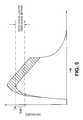
- FIG. 5The effect of the triangular set pulse on cell temperatures in a phase-change memory are illustrated in the exemplary plot of FIG. 5 . It can be seen that even with large variation in temperature (depicted by the shaded band) for a given magnitude and decay rate in the triangular set pulse, the entire memory device is swept through a rapid crystallization temperature interval, so that optimum, i.e. lowest, set resistance is obtained for all cells in the device.
- FIG. 6is a plot of memory cell resistance versus set current for a particular phase-change memory device. The resistance is plotted as the memory cell, beginning in the reset state, responds to the various levels of programming current.
- the sequence for applying the various levels of programming currentis indicated by the arrows, starting from the left and then moving to the right and then coming back to the left.
- the lowest set resistancemay be obtained at a value of set current just prior to its rapid rise towards the reset level.
- the triangular nature of the set pulseallows this lowest set resistance to be ‘locked in’ as the set sweep pulse sweeps back down from its peak value. Assuring the lowest set resistance for each cell in the memory device provides superior margin for memory read operations, higher manufacturing yields, as well as better product reliability.
- FIG. 7depicts a plot of memory cell resistance versus programming current for a large population of memory cells in a memory device.
- This devicesuffers from a relatively wide variation in the population of its constituent memory cells.
- the application (to each cell) of the conventional rectangular pulse of magnitude I resetwill work.
- the conventional programming technique of applying the same rectangular set pulsewould be unable to return every cell in the device to the set state. That's because to do so the current magnitude needs to be at least as high as I conv . But at that magnitude some of the cells, namely those falling within region 704 , will stay at the reset state when the pulse has abruptly ended.
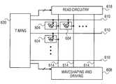
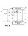
- FIG. 8what is shown is a block diagram of a phase-change material memory device, including waveshaping and driving circuitry that are designed to provide the voltage and current levels needed to program the constituent cells of the device.
- the devicefeatures an array of memory cells 604 where each cell 604 can be accessed by a unique pair of vertical conductors 614 and horizontal conductors 610 .
- the horizontal conductors 610allow a control signal from timing logic 620 to be provided to each cell 604 to close or open a solid state switch therein.
- This solid state switchis in series with a volume of the phase-change material whose other terminal is connected to a power supply or power return node. Current is thus sourced or sunk through the phase-change material when the switch is closed.
- This programming currentis provided through the vertical conductors 614 .
- the sourcing or sinking of the programming currentis performed by either the read circuitry 618 or waveshaping and driving circuitry 608 , depending upon whether a write or read operation is being performed.
- the read circuitry 618may be entirely conventional.
- the waveshaping and driving circuitry 608will be designed so as to provide the voltage and current levels that are needed to program the cells 604 according to the first and second pulses described above, wherein the second pulse has a generally triangular shape.
- the waveshaping circuitrycan be implemented using conventional analog waveshaping circuits such as integrator/ramp circuits, exponential and logarithmic circuits, as well as others.
- the shaped pulsesare then driven by conventional fanout circuitry so that each cell 604 that is connected to a vertical conductor 614 is assured of receiving the desired levels of current and voltage to achieve the set sweep.
- Timing logic 620provides digital control signals to the waveshaping and driving circuitry 608 and the read circuitry 618 so that the latter circuits either measure the resistance of the memory cell 604 (read operation) or provide the reset and set pulses at the correct timing and to the selected memory cell 604 .
- Accesses to the cell 604may be in random fashion where each cell can be accessed individually, or it may be orchestrated according to a row by row basis, depending upon the higher level requirements of the memory system.
- the memory device depicted in FIG. 8may be built using a wide range of different fabrication processes, including a slightly modified version of a conventional complimentary metal oxide semiconductor (CMOS) logic fabrication process.
- CMOScomplimentary metal oxide semiconductor
- the array of cells 604 and the waveshaping and driving circuitry 608may be formed in the same integrated circuit (IC) die if doing so can take advantage of the lower cost of system integration on a single chip.
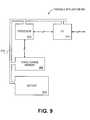
- FIG. 9illustrates a block diagram of a portable application 904 of the phase-change memory programming process described above.
- a phase-change memory 908is operated according to an embodiment of the programming process described above.
- the phase-change memory 908may include one or more integrated circuit dies where each die has a memory array that is programmed according to the various embodiments of the programming techniques described above in FIGS. 1-8. These IC dies may be separate, stand alone memory devices that are arranged in modules such as conventional dynamic random access memory (DRAM) modules, or they may be integrated with other on-chip functionalities. In the latter embodiments, the phase-change memory 908 may be part of an I/O processor or a microcontroller.
- DRAMdynamic random access memory
- the application 904may be for instance a portable notebook computer, a digital still and/or video camera, a personal digital assistant, or a mobile (cellular) hand-held telephone unit.
- an electronic systemincludes a processor 910 that uses the phase-change memory 908 as program memory to store code and data for its execution.
- the phase-change memory 908may be used as a mass storage device for non-volatile storage of code and data.
- the portable application 904communicates with other devices, such as a personal computer or a network of computers via an I/O interface 914 .
- This I/O interface 914may provide access to a computer peripheral bus, a high speed digital communication transmission line, or an antenna for unguided transmissions. Communications between the processor and the phase-change memory 908 and between the processor and the I/O interface 914 may be accomplished using conventional computer bus architectures.
- the above-described components of the portable application 904are powered by a battery 918 via a power supply bus 916 . Since the application 904 is normally battery powered, its functional components including the phase-change memory 908 should be designed to provide the desired performance at low power consumption levels. In addition, due to the restricted size of portable applications, the various components shown in FIG. 9 including the phase-change memory 908 should provide a relatively high density of functionality. Of course, there are other non-portable applications for the phase-change memory 908 that are not shown. These include, for instance, large network servers or other computing devices which may benefit from a non-volatile memory device such as the phase-change memory.
- the phase-change materialmay be Ge2Sb2Te5.
- An exemplary pulsemay have a peak current magnitude of Ireset, where Ireset is sufficiently high to allow the cells of the array to be programmed into the reset state.
- the exemplary pulsemay also have a falling edge that decreases from Ireset to zero current in about 200 nsec.
- phase-change material memory programming techniquereferred to as a set sweep
- set sweepvarious embodiment of a phase-change material memory programming technique
- the phase-change materialmay be a chalcogenide alloy or other suitable structural phase-change material that acts as a programmable resistor.
- the specification and drawingsare, accordingly, to be regarded in an illustrative rather than a restrictive sense.
Landscapes
- Chemical & Material Sciences (AREA)
- Crystallography & Structural Chemistry (AREA)
- Engineering & Computer Science (AREA)
- Computer Hardware Design (AREA)
- Semiconductor Memories (AREA)
Abstract
Description
Claims (60)
Priority Applications (3)
| Application Number | Priority Date | Filing Date | Title |
|---|---|---|---|
| US09/895,135US6570784B2 (en) | 2001-06-29 | 2001-06-29 | Programming a phase-change material memory |
| TW091113634ATWI225652B (en) | 2001-06-29 | 2002-06-21 | Programming a phase-change material memory |
| US10/404,171US6687153B2 (en) | 2001-06-29 | 2003-04-01 | Programming a phase-change material memory |
Applications Claiming Priority (1)
| Application Number | Priority Date | Filing Date | Title |
|---|---|---|---|
| US09/895,135US6570784B2 (en) | 2001-06-29 | 2001-06-29 | Programming a phase-change material memory |
Related Child Applications (1)
| Application Number | Title | Priority Date | Filing Date |
|---|---|---|---|
| US10/404,171DivisionUS6687153B2 (en) | 2001-06-29 | 2003-04-01 | Programming a phase-change material memory |
Publications (2)
| Publication Number | Publication Date |
|---|---|
| US20030002332A1 US20030002332A1 (en) | 2003-01-02 |
| US6570784B2true US6570784B2 (en) | 2003-05-27 |
Family
ID=25404047
Family Applications (2)
| Application Number | Title | Priority Date | Filing Date |
|---|---|---|---|
| US09/895,135Expired - LifetimeUS6570784B2 (en) | 2001-06-29 | 2001-06-29 | Programming a phase-change material memory |
| US10/404,171Expired - LifetimeUS6687153B2 (en) | 2001-06-29 | 2003-04-01 | Programming a phase-change material memory |
Family Applications After (1)
| Application Number | Title | Priority Date | Filing Date |
|---|---|---|---|
| US10/404,171Expired - LifetimeUS6687153B2 (en) | 2001-06-29 | 2003-04-01 | Programming a phase-change material memory |
Country Status (2)
| Country | Link |
|---|---|
| US (2) | US6570784B2 (en) |
| TW (1) | TWI225652B (en) |
Cited By (134)
| Publication number | Priority date | Publication date | Assignee | Title |
|---|---|---|---|---|
| US20020116955A1 (en)* | 2001-02-19 | 2002-08-29 | Sumitomo Electric Industries, Ltd. | Method of forming soot preform |
| US20020168852A1 (en)* | 2001-05-11 | 2002-11-14 | Harshfield Steven T. | PCRAM memory cell and method of making same |
| US20030045049A1 (en)* | 2001-08-29 | 2003-03-06 | Campbell Kristy A. | Method of forming chalcogenide comprising devices |
| US20030047772A1 (en)* | 2001-03-15 | 2003-03-13 | Jiutao Li | Agglomeration elimination for metal sputter deposition of chalcogenides |
| US20030096497A1 (en)* | 2001-11-19 | 2003-05-22 | Micron Technology, Inc. | Electrode structure for use in an integrated circuit |
| US20030117831A1 (en)* | 2001-12-20 | 2003-06-26 | Glen Hush | Programmable conductor random access memory and a method for writing thereto |
| US20030128612A1 (en)* | 2002-01-04 | 2003-07-10 | John Moore | PCRAM rewrite prevention |
| US20030155606A1 (en)* | 2002-02-15 | 2003-08-21 | Campbell Kristy A. | Method to alter chalcogenide glass for improved switching characteristics |
| US20030156468A1 (en)* | 2002-02-20 | 2003-08-21 | Campbell Kristy A. | Resistance variable 'on' memory |
| US20030156463A1 (en)* | 2002-02-19 | 2003-08-21 | Casper Stephen L. | Programmable conductor random access memory and method for sensing same |
| US20030169625A1 (en)* | 2002-03-05 | 2003-09-11 | Glen Hush | Programmable conductor random access memory and method for sensing same |
| US20030173558A1 (en)* | 2002-03-14 | 2003-09-18 | Campbell Kristy A. | Methods and apparatus for resistance variable material cells |
| US20030193059A1 (en)* | 2002-04-10 | 2003-10-16 | Gilton Terry L. | Programmable conductor memory cell structure and method therefor |
| US20030193053A1 (en)* | 2002-04-10 | 2003-10-16 | Gilton Terry L. | Thin film diode integrated with chalcogenide memory cell |
| US20030194865A1 (en)* | 2002-04-10 | 2003-10-16 | Gilton Terry L. | Method of manufacture of programmable conductor memory |
| US20030198118A1 (en)* | 2001-08-02 | 2003-10-23 | Lowery Tyler A. | Method for reading a structural phase-change memory |
| US6674115B2 (en)* | 2001-08-31 | 2004-01-06 | Intel Corporation | Multiple layer phrase-change memory |
| US20040007749A1 (en)* | 2002-07-10 | 2004-01-15 | Campbell Kristy A. | Assemblies displaying differential negative resistance |
| US20040007718A1 (en)* | 2001-08-30 | 2004-01-15 | Campbell Kristy A. | Stoichiometry for chalcogenide glasses useful for memory devices and method of formation |
| US20040022085A1 (en)* | 2002-08-05 | 2004-02-05 | Parkinson Ward D. | Refreshing memory cells of a phase change material memory device |
| US20040029351A1 (en)* | 2002-01-31 | 2004-02-12 | Gilton Terry L. | Methods of forming non-volatile resistance variable devices and methods of forming silver selenide comprising structures |
| US20040038480A1 (en)* | 2002-08-22 | 2004-02-26 | Moore John T. | Method of manufacture of a PCRAM memory cell |
| US20040043553A1 (en)* | 2002-06-06 | 2004-03-04 | Jiutao Li | Elimination of dendrite formation during metal/chalcogenide glass deposition |
| US20040040835A1 (en)* | 2002-08-29 | 2004-03-04 | Jiutao Li | Silver selenide film stoichiometry and morphology control in sputter deposition |
| US20040040837A1 (en)* | 2002-08-29 | 2004-03-04 | Mcteer Allen | Method of forming chalcogenide sputter target |
| US20040043245A1 (en)* | 2002-08-29 | 2004-03-04 | Moore John T. | Method to control silver concentration in a resistance variable memory element |
| US20040053461A1 (en)* | 2002-08-29 | 2004-03-18 | Moore John T. | Graded GexSe100-x concentration in PCRAM |
| US20040114419A1 (en)* | 2002-12-13 | 2004-06-17 | Lowrey Tyler A. | Method and system to store information |
| US20040124406A1 (en)* | 2001-08-29 | 2004-07-01 | Campbell Kristy A. | Method of forming non-volatile resistance variable devices, method of forming a programmable memory cell of memory circuitry, and a non-volatile resistance variable device |
| US20040130598A1 (en)* | 2002-07-10 | 2004-07-08 | Canon Kabushiki Kaisha | Ink jet record head |
| US20040145941A1 (en)* | 2002-10-15 | 2004-07-29 | Rust Thomas F | Phase change media for high density data storage |
| US20040157417A1 (en)* | 2002-08-29 | 2004-08-12 | Moore John T. | Methods to form a memory cell with metal-rich metal chalcogenide |
| US20040161874A1 (en)* | 2001-03-01 | 2004-08-19 | Moore John T. | Method of forming a non-volatile resistance variable device, and non-volatile resistance variable device |
| US20040175859A1 (en)* | 2002-08-29 | 2004-09-09 | Campbell Kristy A. | Single polarity programming of a PCRAM structure |
| US20040180533A1 (en)* | 2003-03-14 | 2004-09-16 | Li Li | Method for filling via with metal |
| US20040179394A1 (en)* | 2003-03-10 | 2004-09-16 | Ovshinsky Stanford R. | Secured phase-change devices |
| US20040192006A1 (en)* | 2002-02-20 | 2004-09-30 | Campbell Kristy A. | Layered resistance variable memory device and method of fabrication |
| US20040202016A1 (en)* | 2003-04-10 | 2004-10-14 | Campbell Kristy A. | Differential negative resistance memory |
| US20040202017A1 (en)* | 2003-04-04 | 2004-10-14 | Se-Ho Lee | Low-current and high-speed phase-change memory devices and methods of driving the same |
| US6809362B2 (en) | 2002-02-20 | 2004-10-26 | Micron Technology, Inc. | Multiple data state memory cell |
| US20040211957A1 (en)* | 2002-08-29 | 2004-10-28 | Moore John T. | Method and apparatus for controlling metal doping of a chalcogenide memory element |
| US6813178B2 (en) | 2003-03-12 | 2004-11-02 | Micron Technology, Inc. | Chalcogenide glass constant current device, and its method of fabrication and operation |
| US20040235235A1 (en)* | 2002-06-06 | 2004-11-25 | Jiutao Li | Co-sputter deposition of metal-doped chalcogenides |
| US20040246804A1 (en)* | 2003-06-03 | 2004-12-09 | Samsung Electronics Co., Ltd. | Device and method for pulse width control in a phase change memory device |
| US6833559B2 (en) | 2001-02-08 | 2004-12-21 | Micron Technology, Inc. | Non-volatile resistance variable device |
| US20040264234A1 (en)* | 2003-06-25 | 2004-12-30 | Moore John T. | PCRAM cell operation method to control on/off resistance variation |
| US20050017233A1 (en)* | 2003-07-21 | 2005-01-27 | Campbell Kristy A. | Performance PCRAM cell |
| US20050018509A1 (en)* | 2001-11-20 | 2005-01-27 | Glen Hush | Complementary bit resistance memory sensor and method of operation |
| US20050026433A1 (en)* | 2001-08-30 | 2005-02-03 | Jiutao Li | Integrated circuit device and fabrication using metal-doped chalcogenide materials |
| US20050036364A1 (en)* | 2003-08-13 | 2005-02-17 | Ha Yong-Ho | Method and driver for programming phase change memory cell |
| US20050054207A1 (en)* | 2002-08-29 | 2005-03-10 | Micron Technology, Inc. | Plasma etching methods and methods of forming memory devices comprising a chalcogenide comprising layer received operably proximate conductive electrodes |
| US20050056910A1 (en)* | 2003-09-17 | 2005-03-17 | Gilton Terry L. | Non-volatile memory structure |
| US20050098814A1 (en)* | 2002-08-20 | 2005-05-12 | Horii Hideki | Methods of fabricating phase changeable memory devices having reduced cell areas |
| US6894304B2 (en) | 2001-08-27 | 2005-05-17 | Micron Technology, Inc. | Apparatus and method for dual cell common electrode PCRAM memory device |
| US20050117387A1 (en)* | 2003-03-27 | 2005-06-02 | Young-Nam Hwang | Phase-change memory and method having restore function |
| US20050122771A1 (en)* | 2003-12-05 | 2005-06-09 | Bomy Chen | Memory device and method of operating same |
| US20050162907A1 (en)* | 2004-01-28 | 2005-07-28 | Campbell Kristy A. | Resistance variable memory elements based on polarized silver-selenide network growth |
| US20050167689A1 (en)* | 2004-01-29 | 2005-08-04 | Campbell Kristy A. | Non-volatile zero field splitting resonance memory |
| US20050195633A1 (en)* | 2004-03-05 | 2005-09-08 | Byung-Gil Choi | Method for programming phase-change memory array to set state and circuit of a phase-change memory device |
| US20050202588A1 (en)* | 2004-03-10 | 2005-09-15 | Brooks Joseph F. | Method of forming a chalcogenide material containing device |
| US20050201174A1 (en)* | 2004-03-10 | 2005-09-15 | Klein Dean A. | Power management control and controlling memory refresh operations |
| US6951805B2 (en) | 2001-08-01 | 2005-10-04 | Micron Technology, Inc. | Method of forming integrated circuitry, method of forming memory circuitry, and method of forming random access memory circuitry |
| US20050232061A1 (en)* | 2004-04-16 | 2005-10-20 | Rust Thomas F | Systems for writing and reading highly resolved domains for high density data storage |
| US20050232004A1 (en)* | 2004-04-16 | 2005-10-20 | Rust Thomas F | Methods for erasing bit cells in a high density data storage device |
| US6961277B2 (en) | 2003-07-08 | 2005-11-01 | Micron Technology, Inc. | Method of refreshing a PCRAM memory device |
| US20050242338A1 (en)* | 2004-04-30 | 2005-11-03 | Hart Mark W | Non-planarized, self-aligned, non-volatile phase-change memory array and method of formation |
| US20060012008A1 (en)* | 2004-07-19 | 2006-01-19 | Campbell Kristy A | Resistance variable memory device and method of fabrication |
| US20060011910A1 (en)* | 2004-07-19 | 2006-01-19 | Micron Technology, Inc. | PCRAM device with switching glass layer |
| US20060033094A1 (en)* | 2004-08-12 | 2006-02-16 | Campbell Kristy A | Resistance variable memory with temperature tolerant materials |
| US20060035403A1 (en)* | 2004-08-12 | 2006-02-16 | Campbell Kristy A | PCRAM device with switching glass layer |
| US20060044906A1 (en)* | 2004-09-01 | 2006-03-02 | Ethan Williford | Sensing of resistance variable memory devices |
| US7010644B2 (en) | 2002-08-29 | 2006-03-07 | Micron Technology, Inc. | Software refreshed memory device and method |
| US20060056233A1 (en)* | 2004-09-10 | 2006-03-16 | Parkinson Ward D | Using a phase change memory as a replacement for a buffered flash memory |
| US20060131556A1 (en)* | 2004-12-22 | 2006-06-22 | Micron Technology, Inc. | Small electrode for resistance variable devices |
| US20060131555A1 (en)* | 2004-12-22 | 2006-06-22 | Micron Technology, Inc. | Resistance variable devices with controllable channels |
| US20060181931A1 (en)* | 2003-08-13 | 2006-08-17 | Ha Yong-Ho | Method and driver for programming phase change memory cell |
| US20060237707A1 (en)* | 2005-04-22 | 2006-10-26 | Micron Technology, Inc. | Memory array for increased bit density and method of forming the same |
| US20060256640A1 (en)* | 2005-05-16 | 2006-11-16 | Micron Technology, Inc. | Power circuits for reducing a number of power supply voltage taps required for sensing a resistive memory |
| US20060270099A1 (en)* | 2001-08-29 | 2006-11-30 | Micron Technology, Inc. | Method of forming non-volatile resistance variable devices and method of forming a programmable memory cell of memory circuitry |
| US20070006455A1 (en)* | 2005-06-24 | 2007-01-11 | Nanochip, Inc. | Methods for forming high density data storage devices with read/write probes with hollow or reinforced tips |
| US20070008768A1 (en)* | 2005-07-08 | 2007-01-11 | Micron Technology, Inc. | Process for erasing chalcogenide variable resistance memory bits |
| US20070008769A1 (en)* | 2005-07-06 | 2007-01-11 | Samsung Electronics Co., Ltd. | Phase-changeable memory device and method of programming the same |
| US20070010054A1 (en)* | 2005-07-08 | 2007-01-11 | Nanochip, Inc. | Method for forming patterned media for a high density data storage device |
| US20070007506A1 (en)* | 2002-02-20 | 2007-01-11 | Micron Technology, Inc. | Layered resistance variable memory device and method of fabrication |
| US20070023744A1 (en)* | 2005-08-01 | 2007-02-01 | Micron Technology, Inc. | Resistance variable memory device with sputtered metal-chalcogenide region and method of fabrication |
| US20070030554A1 (en)* | 2005-08-02 | 2007-02-08 | Micron Technology, Inc. | Method and apparatus for providing color changing thin film material |
| US20070037316A1 (en)* | 2005-08-09 | 2007-02-15 | Micron Technology, Inc. | Memory cell contact using spacers |
| US20070034921A1 (en)* | 2005-08-09 | 2007-02-15 | Micron Technology, Inc. | Access transistor for memory device |
| US20070035990A1 (en)* | 2005-08-15 | 2007-02-15 | Micron Technology, Inc. | Method and apparatus providing a cross-point memory array using a variable resistance memory cell and capacitance |
| US20070047297A1 (en)* | 2005-08-31 | 2007-03-01 | Campbell Kristy A | Resistance variable memory element with threshold device and method of forming the same |
| US20070059882A1 (en)* | 2005-04-22 | 2007-03-15 | Micron Technology, Inc. | Memory elements having patterned electrodes and method of forming the same |
| US7209378B2 (en) | 2002-08-08 | 2007-04-24 | Micron Technology, Inc. | Columnar 1T-N memory cell structure |
| US20070090354A1 (en)* | 2005-08-11 | 2007-04-26 | Micron Technology, Inc. | Chalcogenide-based electrokinetic memory element and method of forming the same |
| US7242019B2 (en)* | 2002-12-13 | 2007-07-10 | Intel Corporation | Shunted phase change memory |
| US7269044B2 (en) | 2005-04-22 | 2007-09-11 | Micron Technology, Inc. | Method and apparatus for accessing a memory array |
| US20070228513A1 (en)* | 2006-03-28 | 2007-10-04 | Min Kyu S | Probe-based memory |
| US7294527B2 (en) | 2002-08-29 | 2007-11-13 | Micron Technology Inc. | Method of forming a memory cell |
| US7317200B2 (en) | 2005-02-23 | 2008-01-08 | Micron Technology, Inc. | SnSe-based limited reprogrammable cell |
| US20080025080A1 (en)* | 2006-07-27 | 2008-01-31 | Cswitch Corporation | Method and apparatus for programming phase change devices |
| US7332735B2 (en) | 2005-08-02 | 2008-02-19 | Micron Technology, Inc. | Phase change memory cell and method of formation |
| US7336524B2 (en) | 2002-10-15 | 2008-02-26 | Nanochip, Inc. | Atomic probes and media for high density data storage |
| US7379412B2 (en) | 2004-04-16 | 2008-05-27 | Nanochip, Inc. | Methods for writing and reading highly resolved domains for high density data storage |
| US7391707B2 (en) | 1998-12-18 | 2008-06-24 | Nanochip, Inc. | Devices and methods of detecting movement between media and probe tip in a probe data storage system |
| US20080151613A1 (en)* | 2006-12-25 | 2008-06-26 | Industrial Technology Research Institute | Programming method for phase change memory |
| US20080170431A1 (en)* | 2007-01-12 | 2008-07-17 | Industrial Technology Research Institute | Driving method and system for a phase change memory |
| US20080219046A1 (en)* | 2007-03-08 | 2008-09-11 | Industrial Technology Research Institute | Writing method and system for a phase change memory |
| US20080273379A1 (en)* | 2006-04-20 | 2008-11-06 | Gordon George A | Programming a normally single phase chalcogenide material for use as a memory of FPLA |
| US7463573B2 (en) | 2005-06-24 | 2008-12-09 | Nanochip, Inc. | Patterned media for a high density data storage device |
| US20080310217A1 (en)* | 2007-06-13 | 2008-12-18 | Pei-Chia Chiang | Writing circuit for a phase change memory |
| US20090073753A1 (en)* | 2005-09-21 | 2009-03-19 | Kenichi Osada | Semiconductor device |
| US20090161415A1 (en)* | 2007-12-21 | 2009-06-25 | Qimonda Ag | Integrated circuit for setting a memory cell based on a reset current distribution |
| US20090244961A1 (en)* | 2008-03-26 | 2009-10-01 | Micron Technology, Incorporated | Phase change memory |
| US20090261316A1 (en)* | 2006-08-29 | 2009-10-22 | Jun Liu | Enhanced memory density resistance variable memory cells, arrays, devices and systems including the same, and methods of fabrication |
| US20100020594A1 (en)* | 2008-07-28 | 2010-01-28 | Stmicroelectronics S.R.L. | Device for programming a pcm cell with discharge of capacitance and method for programming a pcm cell |
| US20100067290A1 (en)* | 2008-09-15 | 2010-03-18 | Savransky Semyon D | Method of programming of phase-change memory and associated devices and materials |
| US20100214829A1 (en)* | 2009-02-24 | 2010-08-26 | International Business Machines Corporation | Memory programming |
| US20100218071A1 (en)* | 2009-02-24 | 2010-08-26 | International Business Machines Corporation | Writing a special symbol to a memory to indicate the absence of a data signal |
| US20110037558A1 (en)* | 2008-08-01 | 2011-02-17 | Boise State University | Continuously variable resistor |
| US20110078387A1 (en)* | 2009-09-28 | 2011-03-31 | International Business Machines Corporation | Writing to memory using shared address buses |
| US20110078392A1 (en)* | 2009-09-28 | 2011-03-31 | International Business Machines Corporation | Writing to memory using adaptive write techniques |
| US7929336B2 (en) | 2008-06-11 | 2011-04-19 | Qimonda Ag | Integrated circuit including a memory element programmed using a seed pulse |
| EP2355105A1 (en) | 2010-02-02 | 2011-08-10 | Nxp B.V. | Phase change memory programming method and phase change memory |
| CN101236779B (en)* | 2007-01-31 | 2012-05-30 | 旺宏电子股份有限公司 | Storage device and programming method thereof |
| US8463985B2 (en) | 2010-03-31 | 2013-06-11 | International Business Machines Corporation | Constrained coding to reduce floating gate coupling in non-volatile memories |
| US8624215B2 (en) | 2005-12-20 | 2014-01-07 | University Of Southampton | Phase change memory devices and methods comprising gallium, lanthanide and chalcogenide compounds |
| US20140160872A1 (en)* | 2012-12-11 | 2014-06-12 | SK Hynix Inc. | Voltage generation circuit, and write driver and semiconductor memory apparatus including the same |
| US9171614B2 (en) | 2008-12-31 | 2015-10-27 | Micron Technology, Inc. | Reliable set operation for phase-change memory cell |
| US9293197B2 (en) | 2011-08-15 | 2016-03-22 | Lockheed Martin Corporation | Reconfigurable phase change material masks for electro-optical compressive sensing |
| US9343149B2 (en)* | 2014-07-10 | 2016-05-17 | Micron Technology, Inc. | Enhancing nucleation in phase-change memory cells |
| US9340446B1 (en) | 2013-02-04 | 2016-05-17 | Lockheed Martin Corporation | Optical apparatus and method of forming a gradient index device |
| US9908808B1 (en) | 2016-08-18 | 2018-03-06 | Lockheed Martin Corporation | Ternary glass materials with low refractive index variability |
| US9969647B2 (en) | 2016-05-17 | 2018-05-15 | Lockheed Martin Energy, Llc | Glass composites having a gradient index of refraction and methods for production thereof |
| US10437083B1 (en) | 2014-10-20 | 2019-10-08 | Lockheed Martin Corporation | Individually addressable infrared mask array |
| US20200066315A1 (en)* | 2018-08-24 | 2020-02-27 | SK Hynix Inc. | Electronic device |
Families Citing this family (52)
| Publication number | Priority date | Publication date | Assignee | Title |
|---|---|---|---|---|
| US6147395A (en)* | 1996-10-02 | 2000-11-14 | Micron Technology, Inc. | Method for fabricating a small area of contact between electrodes |
| US7935951B2 (en)* | 1996-10-28 | 2011-05-03 | Ovonyx, Inc. | Composite chalcogenide materials and devices |
| DE10310573A1 (en)* | 2003-03-11 | 2004-09-30 | Infineon Technologies Ag | Non-volatile, integrated memory cell and method for writing or reading information into / from the memory cell |
| DE102004016408B4 (en)* | 2003-03-27 | 2008-08-07 | Samsung Electronics Co., Ltd., Suwon | Phase change memory module and associated programming method |
| EP1489622B1 (en)* | 2003-06-16 | 2007-08-15 | STMicroelectronics S.r.l. | Writing circuit for a phase change memory device |
| US6965521B2 (en)* | 2003-07-31 | 2005-11-15 | Bae Systems, Information And Electronics Systems Integration, Inc. | Read/write circuit for accessing chalcogenide non-volatile memory cells |
| JP4567963B2 (en) | 2003-12-05 | 2010-10-27 | ルネサスエレクトロニクス株式会社 | Semiconductor integrated circuit device |
| KR100564602B1 (en)* | 2003-12-30 | 2006-03-29 | 삼성전자주식회사 | Set programming method and write driver circuit of phase change memory array |
| DE102005004338B4 (en)* | 2004-02-04 | 2009-04-09 | Samsung Electronics Co., Ltd., Suwon | Phase change memory device and associated programming method |
| US6944041B1 (en)* | 2004-03-26 | 2005-09-13 | Bae Systems Information And Electronic Systems Integration, Inc. | Circuit for accessing a chalcogenide memory array |
| ATE486369T1 (en)* | 2004-03-26 | 2010-11-15 | Nxp Bv | ELECTRICAL DEVICE COMPRISING A PHASE CHANGE MATERIAL |
| KR100618824B1 (en) | 2004-05-08 | 2006-08-31 | 삼성전자주식회사 | Driving circuit and programming method for controlling current pulse width of phase change memory device |
| KR100618836B1 (en)* | 2004-06-19 | 2006-09-08 | 삼성전자주식회사 | Programming Method of Semiconductor Memory Device and Semiconductor Memory Device |
| US7327602B2 (en)* | 2004-10-07 | 2008-02-05 | Ovonyx, Inc. | Methods of accelerated life testing of programmable resistance memory elements |
| KR100564637B1 (en)* | 2004-10-26 | 2006-03-29 | 삼성전자주식회사 | Semiconductor memory device and its programming method |
| KR100564636B1 (en)* | 2004-10-26 | 2006-03-28 | 삼성전자주식회사 | Semiconductor memory device |
| US7272037B2 (en)* | 2004-10-29 | 2007-09-18 | Macronix International Co., Ltd. | Method for programming a multilevel phase change memory device |
| US7495944B2 (en)* | 2005-03-30 | 2009-02-24 | Ovonyx, Inc. | Reading phase change memories |
| KR100855959B1 (en) | 2005-04-04 | 2008-09-02 | 삼성전자주식회사 | Programming Method of Memory Cell Array Using Current Pulse with Pulse Width Control |
| KR100699837B1 (en)* | 2005-04-04 | 2007-03-27 | 삼성전자주식회사 | Programming Method of Semiconductor Memory Device and Semiconductor Memory Device |
| US7525117B2 (en)* | 2005-08-09 | 2009-04-28 | Ovonyx, Inc. | Chalcogenide devices and materials having reduced germanium or telluruim content |
| US7767992B2 (en)* | 2005-08-09 | 2010-08-03 | Ovonyx, Inc. | Multi-layer chalcogenide devices |
| US20070034850A1 (en)* | 2005-08-09 | 2007-02-15 | Ovonyx, Inc. | Chalcogenide devices incorporating chalcogenide materials having reduced germanium or telluruim content |
| US7372725B2 (en)* | 2005-08-15 | 2008-05-13 | Infineon Technologies Ag | Integrated circuit having resistive memory |
| US7796426B2 (en)* | 2005-10-17 | 2010-09-14 | Renesas Technology Corp. | Semiconductor device |
| US20070171705A1 (en)* | 2005-12-15 | 2007-07-26 | Parkinson Ward D | Writing phase change memories |
| US7292466B2 (en)* | 2006-01-03 | 2007-11-06 | Infineon Technologies Ag | Integrated circuit having a resistive memory |
| US7626858B2 (en)* | 2006-06-09 | 2009-12-01 | Qimonda North America Corp. | Integrated circuit having a precharging circuit |
| US7457146B2 (en)* | 2006-06-19 | 2008-11-25 | Qimonda North America Corp. | Memory cell programmed using a temperature controlled set pulse |
| WO2008016833A2 (en)* | 2006-07-31 | 2008-02-07 | Sandisk 3D Llc | Increasing write voltage pulse operations in non-volatile memory |
| US7499355B2 (en)* | 2006-07-31 | 2009-03-03 | Sandisk 3D Llc | High bandwidth one time field-programmable memory |
| US7495947B2 (en)* | 2006-07-31 | 2009-02-24 | Sandisk 3D Llc | Reverse bias trim operations in non-volatile memory |
| US7499304B2 (en)* | 2006-07-31 | 2009-03-03 | Sandisk 3D Llc | Systems for high bandwidth one time field-programmable memory |
| US7492630B2 (en)* | 2006-07-31 | 2009-02-17 | Sandisk 3D Llc | Systems for reverse bias trim operations in non-volatile memory |
| US7522448B2 (en)* | 2006-07-31 | 2009-04-21 | Sandisk 3D Llc | Controlled pulse operations in non-volatile memory |
| US7719874B2 (en)* | 2006-07-31 | 2010-05-18 | Sandisk 3D Llc | Systems for controlled pulse operations in non-volatile memory |
| KR100827703B1 (en)* | 2006-12-14 | 2008-05-07 | 삼성전자주식회사 | Test method of phase change memory device |
| US7969769B2 (en)* | 2007-03-15 | 2011-06-28 | Ovonyx, Inc. | Multi-terminal chalcogenide logic circuits |
| KR100819560B1 (en)* | 2007-03-26 | 2008-04-08 | 삼성전자주식회사 | Phase change memory device and manufacturing method |
| US7704788B2 (en)* | 2007-04-06 | 2010-04-27 | Samsung Electronics Co., Ltd. | Methods of fabricating multi-bit phase-change memory devices and devices formed thereby |
| US7564710B2 (en)* | 2007-04-30 | 2009-07-21 | Qimonda North America Corp. | Circuit for programming a memory element |
| US7571901B2 (en)* | 2007-06-21 | 2009-08-11 | Qimonda North America Corp. | Circuit for programming a memory element |
| US7593255B2 (en) | 2007-12-07 | 2009-09-22 | Qimonda North America Corp. | Integrated circuit for programming a memory element |
| US20090295443A1 (en)* | 2008-06-03 | 2009-12-03 | Qimonda Ag | System and Method For Modifying Signal Characteristics |
| US7978507B2 (en)* | 2008-06-27 | 2011-07-12 | Sandisk 3D, Llc | Pulse reset for non-volatile storage |
| ITTO20080647A1 (en)* | 2008-08-29 | 2010-02-28 | St Microelectronics Srl | COLUMN DECODER FOR NON-VOLATILE MEMORY DEVICES, IN PARTICULAR OF THE PHASE CHANGE TYPE |
| US8386883B2 (en)* | 2009-02-24 | 2013-02-26 | International Business Machines Corporation | Lengthening life of a limited life memory |
| US7944740B2 (en)* | 2009-09-22 | 2011-05-17 | International Business Machines Corporation | Multi-level cell programming of PCM by varying the reset amplitude |
| TWI571872B (en)* | 2013-06-21 | 2017-02-21 | 旺宏電子股份有限公司 | Phase change memory, writing method thereof and reading method thereof |
| CN103714852B (en)* | 2013-12-18 | 2017-03-01 | 华中科技大学 | A kind of precise control micro-nano scale phase change material amorphous rate continually varying method |
| US9543004B1 (en)* | 2015-06-17 | 2017-01-10 | Intel Corporation | Provision of holding current in non-volatile random access memory |
| US9564585B1 (en) | 2015-09-03 | 2017-02-07 | HGST Netherlands B.V. | Multi-level phase change device |
Citations (16)
| Publication number | Priority date | Publication date | Assignee | Title |
|---|---|---|---|---|
| US3271591A (en) | 1963-09-20 | 1966-09-06 | Energy Conversion Devices Inc | Symmetrical current controlling device |
| US3530441A (en) | 1969-01-15 | 1970-09-22 | Energy Conversion Devices Inc | Method and apparatus for storing and retrieving information |
| US5296716A (en) | 1991-01-18 | 1994-03-22 | Energy Conversion Devices, Inc. | Electrically erasable, directly overwritable, multibit single cell memory elements and arrays fabricated therefrom |
| US5687112A (en)* | 1996-04-19 | 1997-11-11 | Energy Conversion Devices, Inc. | Multibit single cell memory element having tapered contact |
| US5789758A (en) | 1995-06-07 | 1998-08-04 | Micron Technology, Inc. | Chalcogenide memory cell with a plurality of chalcogenide electrodes |
| US5879955A (en) | 1995-06-07 | 1999-03-09 | Micron Technology, Inc. | Method for fabricating an array of ultra-small pores for chalcogenide memory cells |
| US5912839A (en)* | 1998-06-23 | 1999-06-15 | Energy Conversion Devices, Inc. | Universal memory element and method of programming same |
| US5933365A (en) | 1997-06-19 | 1999-08-03 | Energy Conversion Devices, Inc. | Memory element with energy control mechanism |
| US5970336A (en) | 1996-08-22 | 1999-10-19 | Micron Technology, Inc. | Method of making memory cell incorporating a chalcogenide element |
| US6031287A (en) | 1997-06-18 | 2000-02-29 | Micron Technology, Inc. | Contact structure and memory element incorporating the same |
| US6075719A (en)* | 1999-06-22 | 2000-06-13 | Energy Conversion Devices, Inc. | Method of programming phase-change memory element |
| US6085341A (en) | 1996-12-31 | 2000-07-04 | Intel Corporation | Memory test mode for wordline resistive defects |
| US6087674A (en) | 1996-10-28 | 2000-07-11 | Energy Conversion Devices, Inc. | Memory element with memory material comprising phase-change material and dielectric material |
| US6141241A (en) | 1998-06-23 | 2000-10-31 | Energy Conversion Devices, Inc. | Universal memory element with systems employing same and apparatus and method for reading, writing and programming same |
| US6229157B1 (en) | 1996-06-18 | 2001-05-08 | Micron Technology, Inc. | Method of forming a polysilicon diode and devices incorporating such diode |
| US6314014B1 (en)* | 1999-12-16 | 2001-11-06 | Ovonyx, Inc. | Programmable resistance memory arrays with reference cells |
Family Cites Families (4)
| Publication number | Priority date | Publication date | Assignee | Title |
|---|---|---|---|---|
| GB1372414A (en) | 1971-11-26 | 1974-10-30 | Marconi Co Ltd | Semiconductor memory device arrangements |
| US6339544B1 (en)* | 2000-09-29 | 2002-01-15 | Intel Corporation | Method to enhance performance of thermal resistor device |
| US6487113B1 (en)* | 2001-06-29 | 2002-11-26 | Ovonyx, Inc. | Programming a phase-change memory with slow quench time |
| US6625054B2 (en)* | 2001-12-28 | 2003-09-23 | Intel Corporation | Method and apparatus to program a phase change memory |
- 2001
- 2001-06-29USUS09/895,135patent/US6570784B2/ennot_activeExpired - Lifetime
- 2002
- 2002-06-21TWTW091113634Apatent/TWI225652B/ennot_activeIP Right Cessation
- 2003
- 2003-04-01USUS10/404,171patent/US6687153B2/ennot_activeExpired - Lifetime
Patent Citations (20)
| Publication number | Priority date | Publication date | Assignee | Title |
|---|---|---|---|---|
| US3271591A (en) | 1963-09-20 | 1966-09-06 | Energy Conversion Devices Inc | Symmetrical current controlling device |
| US3530441A (en) | 1969-01-15 | 1970-09-22 | Energy Conversion Devices Inc | Method and apparatus for storing and retrieving information |
| US5296716A (en) | 1991-01-18 | 1994-03-22 | Energy Conversion Devices, Inc. | Electrically erasable, directly overwritable, multibit single cell memory elements and arrays fabricated therefrom |
| US5789758A (en) | 1995-06-07 | 1998-08-04 | Micron Technology, Inc. | Chalcogenide memory cell with a plurality of chalcogenide electrodes |
| US5879955A (en) | 1995-06-07 | 1999-03-09 | Micron Technology, Inc. | Method for fabricating an array of ultra-small pores for chalcogenide memory cells |
| US5920788A (en) | 1995-06-07 | 1999-07-06 | Micron Technology, Inc. | Chalcogenide memory cell with a plurality of chalcogenide electrodes |
| US6002140A (en) | 1995-06-07 | 1999-12-14 | Micron Technology, Inc. | Method for fabricating an array of ultra-small pores for chalcogenide memory cells |
| US5687112A (en)* | 1996-04-19 | 1997-11-11 | Energy Conversion Devices, Inc. | Multibit single cell memory element having tapered contact |
| US6229157B1 (en) | 1996-06-18 | 2001-05-08 | Micron Technology, Inc. | Method of forming a polysilicon diode and devices incorporating such diode |
| US5998244A (en) | 1996-08-22 | 1999-12-07 | Micron Technology, Inc. | Memory cell incorporating a chalcogenide element and method of making same |
| US5970336A (en) | 1996-08-22 | 1999-10-19 | Micron Technology, Inc. | Method of making memory cell incorporating a chalcogenide element |
| US6153890A (en) | 1996-08-22 | 2000-11-28 | Micron Technology, Inc. | Memory cell incorporating a chalcogenide element |
| US6087674A (en) | 1996-10-28 | 2000-07-11 | Energy Conversion Devices, Inc. | Memory element with memory material comprising phase-change material and dielectric material |
| US6085341A (en) | 1996-12-31 | 2000-07-04 | Intel Corporation | Memory test mode for wordline resistive defects |
| US6031287A (en) | 1997-06-18 | 2000-02-29 | Micron Technology, Inc. | Contact structure and memory element incorporating the same |
| US5933365A (en) | 1997-06-19 | 1999-08-03 | Energy Conversion Devices, Inc. | Memory element with energy control mechanism |
| US6141241A (en) | 1998-06-23 | 2000-10-31 | Energy Conversion Devices, Inc. | Universal memory element with systems employing same and apparatus and method for reading, writing and programming same |
| US5912839A (en)* | 1998-06-23 | 1999-06-15 | Energy Conversion Devices, Inc. | Universal memory element and method of programming same |
| US6075719A (en)* | 1999-06-22 | 2000-06-13 | Energy Conversion Devices, Inc. | Method of programming phase-change memory element |
| US6314014B1 (en)* | 1999-12-16 | 2001-11-06 | Ovonyx, Inc. | Programmable resistance memory arrays with reference cells |
Cited By (402)
| Publication number | Priority date | Publication date | Assignee | Title |
|---|---|---|---|---|
| US7391707B2 (en) | 1998-12-18 | 2008-06-24 | Nanochip, Inc. | Devices and methods of detecting movement between media and probe tip in a probe data storage system |
| US7030410B2 (en) | 2001-02-08 | 2006-04-18 | Micron Technology, Inc. | Resistance variable device |
| US20050019699A1 (en)* | 2001-02-08 | 2005-01-27 | Moore John T. | Non-volatile resistance variable device |
| US6833559B2 (en) | 2001-02-08 | 2004-12-21 | Micron Technology, Inc. | Non-volatile resistance variable device |
| US20020116955A1 (en)* | 2001-02-19 | 2002-08-29 | Sumitomo Electric Industries, Ltd. | Method of forming soot preform |
| US7199444B2 (en) | 2001-03-01 | 2007-04-03 | Micron Technology, Inc. | Memory device, programmable resistance memory cell and memory array |
| US20040161874A1 (en)* | 2001-03-01 | 2004-08-19 | Moore John T. | Method of forming a non-volatile resistance variable device, and non-volatile resistance variable device |
| US6949402B2 (en) | 2001-03-01 | 2005-09-27 | Micron Technology, Inc. | Method of forming a non-volatile resistance variable device |
| US7022555B2 (en) | 2001-03-01 | 2006-04-04 | Micron Technology, Inc. | Methods of forming a semiconductor memory device |
| US20040144968A1 (en)* | 2001-03-15 | 2004-07-29 | Jiutao Li | Agglomeration elimination for metal sputter deposition of chalcogenides |
| US20040144973A1 (en)* | 2001-03-15 | 2004-07-29 | Jiutao Li | Agglomeration elimination for metal sputter deposition of chalcogenides |
| US7528401B2 (en) | 2001-03-15 | 2009-05-05 | Micron Technology, Inc. | Agglomeration elimination for metal sputter deposition of chalcogenides |
| US6878569B2 (en)* | 2001-03-15 | 2005-04-12 | Micron Technology, Inc. | Agglomeration elimination for metal sputter deposition of chalcogenides |
| US20030047772A1 (en)* | 2001-03-15 | 2003-03-13 | Jiutao Li | Agglomeration elimination for metal sputter deposition of chalcogenides |
| US6949453B2 (en) | 2001-03-15 | 2005-09-27 | Micron Technology, Inc. | Agglomeration elimination for metal sputter deposition of chalcogenides |
| US6974965B2 (en) | 2001-03-15 | 2005-12-13 | Micron Technology, Inc. | Agglomeration elimination for metal sputter deposition of chalcogenides |
| US7687793B2 (en) | 2001-05-11 | 2010-03-30 | Micron Technology, Inc. | Resistance variable memory cells |
| US7235419B2 (en) | 2001-05-11 | 2007-06-26 | Micron Technology, Inc. | Method of making a memory cell |
| US20020168852A1 (en)* | 2001-05-11 | 2002-11-14 | Harshfield Steven T. | PCRAM memory cell and method of making same |
| US20070235712A1 (en)* | 2001-05-11 | 2007-10-11 | Harshfield Steven T | Resistance variable memory cells |
| US20060099822A1 (en)* | 2001-05-11 | 2006-05-11 | Harshfield Steven T | Method of making a memory cell |
| US7071021B2 (en) | 2001-05-11 | 2006-07-04 | Micron Technology, Inc. | PCRAM memory cell and method of making same |
| US6951805B2 (en) | 2001-08-01 | 2005-10-04 | Micron Technology, Inc. | Method of forming integrated circuitry, method of forming memory circuitry, and method of forming random access memory circuitry |
| US20030198118A1 (en)* | 2001-08-02 | 2003-10-23 | Lowery Tyler A. | Method for reading a structural phase-change memory |
| US6707712B2 (en)* | 2001-08-02 | 2004-03-16 | Intel Corporation | Method for reading a structural phase-change memory |
| US6894304B2 (en) | 2001-08-27 | 2005-05-17 | Micron Technology, Inc. | Apparatus and method for dual cell common electrode PCRAM memory device |
| US6955940B2 (en) | 2001-08-29 | 2005-10-18 | Micron Technology, Inc. | Method of forming chalcogenide comprising devices |
| US6998697B2 (en) | 2001-08-29 | 2006-02-14 | Micron Technology, Inc. | Non-volatile resistance variable devices |
| US7348205B2 (en) | 2001-08-29 | 2008-03-25 | Micron Technology, Inc. | Method of forming resistance variable devices |
| US20040124406A1 (en)* | 2001-08-29 | 2004-07-01 | Campbell Kristy A. | Method of forming non-volatile resistance variable devices, method of forming a programmable memory cell of memory circuitry, and a non-volatile resistance variable device |
| US20050157573A1 (en)* | 2001-08-29 | 2005-07-21 | Campbell Kristy A. | Method of forming non-volatile resistance variable devices |
| US7863597B2 (en) | 2001-08-29 | 2011-01-04 | Micron Technology, Inc. | Resistance variable memory devices with passivating material |
| US20030045049A1 (en)* | 2001-08-29 | 2003-03-06 | Campbell Kristy A. | Method of forming chalcogenide comprising devices |
| US20080185574A1 (en)* | 2001-08-29 | 2008-08-07 | Campbell Kristy A | Method of forming non-volatile resistance variable devices |
| US20060270099A1 (en)* | 2001-08-29 | 2006-11-30 | Micron Technology, Inc. | Method of forming non-volatile resistance variable devices and method of forming a programmable memory cell of memory circuitry |
| US7396699B2 (en) | 2001-08-29 | 2008-07-08 | Micron Technology, Inc. | Method of forming non-volatile resistance variable devices and method of forming a programmable memory cell of memory circuitry |
| US20040007718A1 (en)* | 2001-08-30 | 2004-01-15 | Campbell Kristy A. | Stoichiometry for chalcogenide glasses useful for memory devices and method of formation |
| US20050026433A1 (en)* | 2001-08-30 | 2005-02-03 | Jiutao Li | Integrated circuit device and fabrication using metal-doped chalcogenide materials |
| US6888155B2 (en) | 2001-08-30 | 2005-05-03 | Micron Technology, Inc. | Stoichiometry for chalcogenide glasses useful for memory devices and method of formation |
| US6674115B2 (en)* | 2001-08-31 | 2004-01-06 | Intel Corporation | Multiple layer phrase-change memory |
| US20030096497A1 (en)* | 2001-11-19 | 2003-05-22 | Micron Technology, Inc. | Electrode structure for use in an integrated circuit |
| US7115504B2 (en) | 2001-11-19 | 2006-10-03 | Micron Technology, Inc. | Method of forming electrode structure for use in an integrated circuit |
| US7332401B2 (en) | 2001-11-19 | 2008-02-19 | Micron Technology, Ing. | Method of fabricating an electrode structure for use in an integrated circuit |
| US20040232551A1 (en)* | 2001-11-19 | 2004-11-25 | Moore John T. | Electrode structure for use in an integrated circuit |
| US7115992B2 (en) | 2001-11-19 | 2006-10-03 | Micron Technology, Inc. | Electrode structure for use in an integrated circuit |
| US20040238958A1 (en)* | 2001-11-19 | 2004-12-02 | Moore John T. | Electrode structure for use in an integrated circuit |
| US20040229423A1 (en)* | 2001-11-19 | 2004-11-18 | Moore John T. | Electrode structure for use in an integrated circuit |
| US6815818B2 (en)* | 2001-11-19 | 2004-11-09 | Micron Technology, Inc. | Electrode structure for use in an integrated circuit |
| US20060245234A1 (en)* | 2001-11-20 | 2006-11-02 | Glen Hush | Method of operating a complementary bit resistance memory sensor and method of operation |
| US7366003B2 (en) | 2001-11-20 | 2008-04-29 | Micron Technology, Inc. | Method of operating a complementary bit resistance memory sensor and method of operation |
| US7002833B2 (en) | 2001-11-20 | 2006-02-21 | Micron Technology, Inc. | Complementary bit resistance memory sensor and method of operation |
| US20050018509A1 (en)* | 2001-11-20 | 2005-01-27 | Glen Hush | Complementary bit resistance memory sensor and method of operation |
| US7242603B2 (en) | 2001-11-20 | 2007-07-10 | Micron Technology, Inc. | Method of operating a complementary bit resistance memory sensor |
| US7869249B2 (en) | 2001-11-20 | 2011-01-11 | Micron Technology, Inc. | Complementary bit PCRAM sense amplifier and method of operation |
| US20060023532A1 (en)* | 2001-11-20 | 2006-02-02 | Glen Hush | Method of operating a complementary bit resistance memory sensor |
| US20030117831A1 (en)* | 2001-12-20 | 2003-06-26 | Glen Hush | Programmable conductor random access memory and a method for writing thereto |
| US6873538B2 (en) | 2001-12-20 | 2005-03-29 | Micron Technology, Inc. | Programmable conductor random access memory and a method for writing thereto |
| US6909656B2 (en) | 2002-01-04 | 2005-06-21 | Micron Technology, Inc. | PCRAM rewrite prevention |
| US6882578B2 (en) | 2002-01-04 | 2005-04-19 | Micron Technology, Inc. | PCRAM rewrite prevention |
| US20030128612A1 (en)* | 2002-01-04 | 2003-07-10 | John Moore | PCRAM rewrite prevention |
| US7224632B2 (en) | 2002-01-04 | 2007-05-29 | Micron Technology, Inc. | Rewrite prevention in a variable resistance memory |
| US20050146958A1 (en)* | 2002-01-04 | 2005-07-07 | John Moore | Rewrite prevention in a variable resistance memory |
| US6812087B2 (en) | 2002-01-31 | 2004-11-02 | Micron Technology, Inc. | Methods of forming non-volatile resistance variable devices and methods of forming silver selenide comprising structures |
| US20040029351A1 (en)* | 2002-01-31 | 2004-02-12 | Gilton Terry L. | Methods of forming non-volatile resistance variable devices and methods of forming silver selenide comprising structures |
| US20040223390A1 (en)* | 2002-02-15 | 2004-11-11 | Campbell Kristy A. | Resistance variable memory element having chalcogenide glass for improved switching characteristics |
| US20030155606A1 (en)* | 2002-02-15 | 2003-08-21 | Campbell Kristy A. | Method to alter chalcogenide glass for improved switching characteristics |
| US6867064B2 (en) | 2002-02-15 | 2005-03-15 | Micron Technology, Inc. | Method to alter chalcogenide glass for improved switching characteristics |
| US20050018493A1 (en)* | 2002-02-19 | 2005-01-27 | Casper Stephen L. | Programmable conductor random access memory and method for sensing same |
| US20030156463A1 (en)* | 2002-02-19 | 2003-08-21 | Casper Stephen L. | Programmable conductor random access memory and method for sensing same |
| US6954385B2 (en) | 2002-02-19 | 2005-10-11 | Micron Technology, Inc. | Method and apparatus for sensing resistive memory state |
| US6791885B2 (en) | 2002-02-19 | 2004-09-14 | Micron Technology, Inc. | Programmable conductor random access memory and method for sensing same |
| US20070007506A1 (en)* | 2002-02-20 | 2007-01-11 | Micron Technology, Inc. | Layered resistance variable memory device and method of fabrication |
| US7498231B2 (en) | 2002-02-20 | 2009-03-03 | Micron Technology, Inc. | Multiple data state memory cell |
| US20030156468A1 (en)* | 2002-02-20 | 2003-08-21 | Campbell Kristy A. | Resistance variable 'on' memory |
| US7087919B2 (en) | 2002-02-20 | 2006-08-08 | Micron Technology, Inc. | Layered resistance variable memory device and method of fabrication |
| US20050157567A1 (en)* | 2002-02-20 | 2005-07-21 | Gilton Terry L. | Multiple data state memory cell |
| US7202520B2 (en) | 2002-02-20 | 2007-04-10 | Micron Technology, Inc. | Multiple data state memory cell |
| US6908808B2 (en) | 2002-02-20 | 2005-06-21 | Micron Technology, Inc. | Method of forming and storing data in a multiple state memory cell |
| US20040192006A1 (en)* | 2002-02-20 | 2004-09-30 | Campbell Kristy A. | Layered resistance variable memory device and method of fabrication |
| US7723713B2 (en) | 2002-02-20 | 2010-05-25 | Micron Technology, Inc. | Layered resistance variable memory device and method of fabrication |
| US6809362B2 (en) | 2002-02-20 | 2004-10-26 | Micron Technology, Inc. | Multiple data state memory cell |
| US20100219391A1 (en)* | 2002-02-20 | 2010-09-02 | Campbell Kristy A | Layered resistance variable memory device and method of fabrication |
| US20070128792A1 (en)* | 2002-02-20 | 2007-06-07 | Micron Technology, Inc. | Multiple data state memory cell |
| US8263958B2 (en) | 2002-02-20 | 2012-09-11 | Micron Technology, Inc. | Layered resistance variable memory device and method of fabrication |
| US20040223357A1 (en)* | 2002-02-20 | 2004-11-11 | Gilton Terry L. | Multiple data state memory cell |
| US6891749B2 (en) | 2002-02-20 | 2005-05-10 | Micron Technology, Inc. | Resistance variable ‘on ’ memory |
| US6937528B2 (en) | 2002-03-05 | 2005-08-30 | Micron Technology, Inc. | Variable resistance memory and method for sensing same |
| US20030169625A1 (en)* | 2002-03-05 | 2003-09-11 | Glen Hush | Programmable conductor random access memory and method for sensing same |
| US6849868B2 (en) | 2002-03-14 | 2005-02-01 | Micron Technology, Inc. | Methods and apparatus for resistance variable material cells |
| US20030173558A1 (en)* | 2002-03-14 | 2003-09-18 | Campbell Kristy A. | Methods and apparatus for resistance variable material cells |
| US6864500B2 (en) | 2002-04-10 | 2005-03-08 | Micron Technology, Inc. | Programmable conductor memory cell structure |
| US20030193059A1 (en)* | 2002-04-10 | 2003-10-16 | Gilton Terry L. | Programmable conductor memory cell structure and method therefor |
| US6855975B2 (en) | 2002-04-10 | 2005-02-15 | Micron Technology, Inc. | Thin film diode integrated with chalcogenide memory cell |
| US20060243973A1 (en)* | 2002-04-10 | 2006-11-02 | Micron Technology, Inc. | Thin film diode integrated with chalcogenide memory cell |
| US20030193053A1 (en)* | 2002-04-10 | 2003-10-16 | Gilton Terry L. | Thin film diode integrated with chalcogenide memory cell |
| US6858482B2 (en) | 2002-04-10 | 2005-02-22 | Micron Technology, Inc. | Method of manufacture of programmable switching circuits and memory cells employing a glass layer |
| US20040171208A1 (en)* | 2002-04-10 | 2004-09-02 | Gilton Terry L. | Method of manufacture of programmable conductor memory |
| US20050101084A1 (en)* | 2002-04-10 | 2005-05-12 | Gilton Terry L. | Thin film diode integrated with chalcogenide memory cell |
| US20030194865A1 (en)* | 2002-04-10 | 2003-10-16 | Gilton Terry L. | Method of manufacture of programmable conductor memory |
| US7112484B2 (en) | 2002-04-10 | 2006-09-26 | Micron Technology, Inc. | Thin film diode integrated with chalcogenide memory cell |
| US7479650B2 (en) | 2002-04-10 | 2009-01-20 | Micron Technology, Inc. | Method of manufacture of programmable conductor memory |
| US7547905B2 (en) | 2002-04-10 | 2009-06-16 | Micron Technology, Inc. | Programmable conductor memory cell structure and method therefor |
| US7964436B2 (en) | 2002-06-06 | 2011-06-21 | Round Rock Research, Llc | Co-sputter deposition of metal-doped chalcogenides |
| US20040235235A1 (en)* | 2002-06-06 | 2004-11-25 | Jiutao Li | Co-sputter deposition of metal-doped chalcogenides |
| US7202104B2 (en) | 2002-06-06 | 2007-04-10 | Micron Technology, Inc. | Co-sputter deposition of metal-doped chalcogenides |
| US7446393B2 (en) | 2002-06-06 | 2008-11-04 | Micron Technology, Inc. | Co-sputter deposition of metal-doped chalcogenides |
| US20090098717A1 (en)* | 2002-06-06 | 2009-04-16 | Jiutao Li | Co-sputter deposition of metal-doped chalcogenides |
| US20040043553A1 (en)* | 2002-06-06 | 2004-03-04 | Jiutao Li | Elimination of dendrite formation during metal/chalcogenide glass deposition |
| US6858465B2 (en) | 2002-06-06 | 2005-02-22 | Micron Technology, Inc. | Elimination of dendrite formation during metal/chalcogenide glass deposition |
| US6890790B2 (en) | 2002-06-06 | 2005-05-10 | Micron Technology, Inc. | Co-sputter deposition of metal-doped chalcogenides |
| US7879646B2 (en) | 2002-07-10 | 2011-02-01 | Micron Technology, Inc. | Assemblies displaying differential negative resistance, semiconductor constructions, and methods of forming assemblies displaying differential negative resistance |
| US20040007749A1 (en)* | 2002-07-10 | 2004-01-15 | Campbell Kristy A. | Assemblies displaying differential negative resistance |
| US20080188034A1 (en)* | 2002-07-10 | 2008-08-07 | Campbell Kristy A | Assemblies displaying differential negative resistance, semiconductor constructions, and methods of forming assemblies displaying differential negative resistance |
| US20040130598A1 (en)* | 2002-07-10 | 2004-07-08 | Canon Kabushiki Kaisha | Ink jet record head |
| US7015494B2 (en) | 2002-07-10 | 2006-03-21 | Micron Technology, Inc. | Assemblies displaying differential negative resistance |
| US20050247927A1 (en)* | 2002-07-10 | 2005-11-10 | Campbell Kristy A | Assemblies displaying differential negative resistance |
| US20040022085A1 (en)* | 2002-08-05 | 2004-02-05 | Parkinson Ward D. | Refreshing memory cells of a phase change material memory device |
| US6768665B2 (en)* | 2002-08-05 | 2004-07-27 | Intel Corporation | Refreshing memory cells of a phase change material memory device |
| US7209378B2 (en) | 2002-08-08 | 2007-04-24 | Micron Technology, Inc. | Columnar 1T-N memory cell structure |
| US20050098814A1 (en)* | 2002-08-20 | 2005-05-12 | Horii Hideki | Methods of fabricating phase changeable memory devices having reduced cell areas |
| US7018863B2 (en) | 2002-08-22 | 2006-03-28 | Micron Technology, Inc. | Method of manufacture of a resistance variable memory cell |
| US20040038480A1 (en)* | 2002-08-22 | 2004-02-26 | Moore John T. | Method of manufacture of a PCRAM memory cell |
| US7550818B2 (en) | 2002-08-22 | 2009-06-23 | Micron Technology, Inc. | Method of manufacture of a PCRAM memory cell |
| US20040238918A1 (en)* | 2002-08-22 | 2004-12-02 | Moore John T. | Method of manufacture of a PCRAM memory cell |
| US20060234425A1 (en)* | 2002-08-22 | 2006-10-19 | Micron Technology, Inc. | Method of manufacture of a PCRAM memory cell |
| US7459764B2 (en) | 2002-08-22 | 2008-12-02 | Micron Technology, Inc. | Method of manufacture of a PCRAM memory cell |
| US7223627B2 (en) | 2002-08-29 | 2007-05-29 | Micron Technology, Inc. | Memory element and its method of formation |
| US6864521B2 (en) | 2002-08-29 | 2005-03-08 | Micron Technology, Inc. | Method to control silver concentration in a resistance variable memory element |
| US20050148150A1 (en)* | 2002-08-29 | 2005-07-07 | Moore John T. | Memory element and its method of formation |
| US20060252176A1 (en)* | 2002-08-29 | 2006-11-09 | Micron Technology, Inc. | Memory element and its method of formation |
| US20040185625A1 (en)* | 2002-08-29 | 2004-09-23 | Moore John T. | Graded GexSe100-x concentration in PCRAM |
| US7364644B2 (en) | 2002-08-29 | 2008-04-29 | Micron Technology, Inc. | Silver selenide film stoichiometry and morphology control in sputter deposition |
| US7944768B2 (en) | 2002-08-29 | 2011-05-17 | Micron Technology, Inc. | Software refreshed memory device and method |
| US7518212B2 (en) | 2002-08-29 | 2009-04-14 | Micron Technology, Inc. | Graded GexSe100-x concentration in PCRAM |
| US7010644B2 (en) | 2002-08-29 | 2006-03-07 | Micron Technology, Inc. | Software refreshed memory device and method |
| US9552986B2 (en) | 2002-08-29 | 2017-01-24 | Micron Technology, Inc. | Forming a memory device using sputtering to deposit silver-selenide film |
| US20050266635A1 (en)* | 2002-08-29 | 2005-12-01 | Moore John T | Graded GexSe100-x concentration in PCRAM |
| US20040157417A1 (en)* | 2002-08-29 | 2004-08-12 | Moore John T. | Methods to form a memory cell with metal-rich metal chalcogenide |
| US6953720B2 (en) | 2002-08-29 | 2005-10-11 | Micron Technology, Inc. | Methods for forming chalcogenide glass-based memory elements |
| US20040043245A1 (en)* | 2002-08-29 | 2004-03-04 | Moore John T. | Method to control silver concentration in a resistance variable memory element |
| US7564731B2 (en) | 2002-08-29 | 2009-07-21 | Micron Technology, Inc. | Software refreshed memory device and method |
| US7692177B2 (en) | 2002-08-29 | 2010-04-06 | Micron Technology, Inc. | Resistance variable memory element and its method of formation |
| US7307908B2 (en) | 2002-08-29 | 2007-12-11 | Micron Technology, Inc. | Software refreshed memory device and method |
| US6867114B2 (en) | 2002-08-29 | 2005-03-15 | Micron Technology Inc. | Methods to form a memory cell with metal-rich metal chalcogenide |
| US20050098428A1 (en)* | 2002-08-29 | 2005-05-12 | Jiutao Li | Silver selenide film stoichiometry and morphology control in sputter deposition |
| US20060104142A1 (en)* | 2002-08-29 | 2006-05-18 | Gilton Terry L | Software refreshed memory device and method |
| US7049009B2 (en) | 2002-08-29 | 2006-05-23 | Micron Technology, Inc. | Silver selenide film stoichiometry and morphology control in sputter deposition |
| US7163837B2 (en) | 2002-08-29 | 2007-01-16 | Micron Technology, Inc. | Method of forming a resistance variable memory element |
| US7056762B2 (en) | 2002-08-29 | 2006-06-06 | Micron Technology, Inc. | Methods to form a memory cell with metal-rich metal chalcogenide |
| US20080210921A1 (en)* | 2002-08-29 | 2008-09-04 | Jiutao Li | Silver selenide film stoichiometry and morphology control in sputter deposition |
| US7294527B2 (en) | 2002-08-29 | 2007-11-13 | Micron Technology Inc. | Method of forming a memory cell |
| US20040040835A1 (en)* | 2002-08-29 | 2004-03-04 | Jiutao Li | Silver selenide film stoichiometry and morphology control in sputter deposition |
| US20070258308A1 (en)* | 2002-08-29 | 2007-11-08 | Gilton Terry L | Software refreshed memory device and method |
| US20090257299A1 (en)* | 2002-08-29 | 2009-10-15 | Gilton Terry L | Software refreshed memory device and method |
| US6867996B2 (en) | 2002-08-29 | 2005-03-15 | Micron Technology, Inc. | Single-polarity programmable resistance-variable memory element |
| US20040053461A1 (en)* | 2002-08-29 | 2004-03-18 | Moore John T. | Graded GexSe100-x concentration in PCRAM |
| US20040040837A1 (en)* | 2002-08-29 | 2004-03-04 | Mcteer Allen | Method of forming chalcogenide sputter target |
| US7087454B2 (en) | 2002-08-29 | 2006-08-08 | Micron Technology, Inc. | Fabrication of single polarity programmable resistance structure |
| US6856002B2 (en) | 2002-08-29 | 2005-02-15 | Micron Technology, Inc. | Graded GexSe100-x concentration in PCRAM |
| US7768861B2 (en) | 2002-08-29 | 2010-08-03 | Micron Technology, Inc. | Software refreshed memory device and method |
| US20040175859A1 (en)* | 2002-08-29 | 2004-09-09 | Campbell Kristy A. | Single polarity programming of a PCRAM structure |
| US20040211957A1 (en)* | 2002-08-29 | 2004-10-28 | Moore John T. | Method and apparatus for controlling metal doping of a chalcogenide memory element |
| US20050054207A1 (en)* | 2002-08-29 | 2005-03-10 | Micron Technology, Inc. | Plasma etching methods and methods of forming memory devices comprising a chalcogenide comprising layer received operably proximate conductive electrodes |
| US7094700B2 (en) | 2002-08-29 | 2006-08-22 | Micron Technology, Inc. | Plasma etching methods and methods of forming memory devices comprising a chalcogenide comprising layer received operably proximate conductive electrodes |
| US6985377B2 (en) | 2002-10-15 | 2006-01-10 | Nanochip, Inc. | Phase change media for high density data storage |
| US20040145941A1 (en)* | 2002-10-15 | 2004-07-29 | Rust Thomas F | Phase change media for high density data storage |
| US7336524B2 (en) | 2002-10-15 | 2008-02-26 | Nanochip, Inc. | Atomic probes and media for high density data storage |
| US6813177B2 (en)* | 2002-12-13 | 2004-11-02 | Ovoynx, Inc. | Method and system to store information |
| US7242019B2 (en)* | 2002-12-13 | 2007-07-10 | Intel Corporation | Shunted phase change memory |
| US20040114419A1 (en)* | 2002-12-13 | 2004-06-17 | Lowrey Tyler A. | Method and system to store information |
| US20040179394A1 (en)* | 2003-03-10 | 2004-09-16 | Ovshinsky Stanford R. | Secured phase-change devices |
| US7085155B2 (en)* | 2003-03-10 | 2006-08-01 | Energy Conversion Devices, Inc. | Secured phase-change devices |
| US6813178B2 (en) | 2003-03-12 | 2004-11-02 | Micron Technology, Inc. | Chalcogenide glass constant current device, and its method of fabrication and operation |
| US20040180533A1 (en)* | 2003-03-14 | 2004-09-16 | Li Li | Method for filling via with metal |
| US7022579B2 (en) | 2003-03-14 | 2006-04-04 | Micron Technology, Inc. | Method for filling via with metal |
| US7042760B2 (en)* | 2003-03-27 | 2006-05-09 | Samsung Electronics Co., Ltd. | Phase-change memory and method having restore function |
| US20050117387A1 (en)* | 2003-03-27 | 2005-06-02 | Young-Nam Hwang | Phase-change memory and method having restore function |
| US7130214B2 (en) | 2003-04-04 | 2006-10-31 | Samsung Electronics Co., Ltd. | Low-current and high-speed phase-change memory devices and methods of driving the same |
| US6967865B2 (en)* | 2003-04-04 | 2005-11-22 | Samsung Electronics Co., Ltd. | Low-current and high-speed phase-change memory devices and methods of driving the same |
| US20040202017A1 (en)* | 2003-04-04 | 2004-10-14 | Se-Ho Lee | Low-current and high-speed phase-change memory devices and methods of driving the same |
| US20050275433A1 (en)* | 2003-04-04 | 2005-12-15 | Se-Ho Lee | Low-current and high-speed phase-change memory devices and methods of driving the same |
| US20080128674A1 (en)* | 2003-04-10 | 2008-06-05 | Campbell Kristy A | Differential negative resistance memory |
| US7329558B2 (en) | 2003-04-10 | 2008-02-12 | Micron Technology, Inc. | Differential negative resistance memory |
| US7050327B2 (en) | 2003-04-10 | 2006-05-23 | Micron Technology, Inc. | Differential negative resistance memory |
| US20040202016A1 (en)* | 2003-04-10 | 2004-10-14 | Campbell Kristy A. | Differential negative resistance memory |
| US7745808B2 (en) | 2003-04-10 | 2010-06-29 | Micron Technology, Inc. | Differential negative resistance memory |
| US7180771B2 (en) | 2003-06-03 | 2007-02-20 | Samsung Electronics Co., Ltd. | Device and method for pulse width control in a phase change memory device |
| US7085154B2 (en)* | 2003-06-03 | 2006-08-01 | Samsung Electronics Co., Ltd. | Device and method for pulse width control in a phase change memory device |
| US20040246804A1 (en)* | 2003-06-03 | 2004-12-09 | Samsung Electronics Co., Ltd. | Device and method for pulse width control in a phase change memory device |
| DE102004025975B4 (en)* | 2003-06-03 | 2010-11-11 | Samsung Electronics Co., Ltd., Suwon | Phase change memory device and programming method |
| US20060181932A1 (en)* | 2003-06-03 | 2006-08-17 | Samsung Electronics, Co., Ltd. | Device and method for pulse width control in a phase change memory device |
| US6930909B2 (en) | 2003-06-25 | 2005-08-16 | Micron Technology, Inc. | Memory device and methods of controlling resistance variation and resistance profile drift |
| US20040264234A1 (en)* | 2003-06-25 | 2004-12-30 | Moore John T. | PCRAM cell operation method to control on/off resistance variation |
| US7385868B2 (en) | 2003-07-08 | 2008-06-10 | Micron Technology, Inc. | Method of refreshing a PCRAM memory device |
| US6961277B2 (en) | 2003-07-08 | 2005-11-01 | Micron Technology, Inc. | Method of refreshing a PCRAM memory device |
| US7061004B2 (en) | 2003-07-21 | 2006-06-13 | Micron Technology, Inc. | Resistance variable memory elements and methods of formation |
| US20050017233A1 (en)* | 2003-07-21 | 2005-01-27 | Campbell Kristy A. | Performance PCRAM cell |
| DE102004039977B4 (en)* | 2003-08-13 | 2008-09-11 | Samsung Electronics Co., Ltd., Suwon | Programming method and driver circuit for a phase change memory cell |
| US20050036364A1 (en)* | 2003-08-13 | 2005-02-17 | Ha Yong-Ho | Method and driver for programming phase change memory cell |
| US7126846B2 (en) | 2003-08-13 | 2006-10-24 | Samsung Electronics Co., Ltd. | Method and driver for programming phase change memory cell |
| US7126847B2 (en) | 2003-08-13 | 2006-10-24 | Samsung Electronics Co., Ltd | Method and driver for programming phase change memory cell |
| US7082051B2 (en)* | 2003-08-13 | 2006-07-25 | Samsung Electronics Co., Ltd. | Method and driver for programming phase change memory cell |
| US20060181933A1 (en)* | 2003-08-13 | 2006-08-17 | Ha Yong-Ho | Method and driver for programming phase change memory cell |
| US20060181931A1 (en)* | 2003-08-13 | 2006-08-17 | Ha Yong-Ho | Method and driver for programming phase change memory cell |
| US6946347B2 (en) | 2003-09-17 | 2005-09-20 | Micron Technology, Inc. | Non-volatile memory structure |
| US6903361B2 (en) | 2003-09-17 | 2005-06-07 | Micron Technology, Inc. | Non-volatile memory structure |
| US7491963B2 (en) | 2003-09-17 | 2009-02-17 | Micron Technology, Inc. | Non-volatile memory structure |
| US20050059187A1 (en)* | 2003-09-17 | 2005-03-17 | Gilton Terry L. | Non-volatile memory structure |
| US20050056910A1 (en)* | 2003-09-17 | 2005-03-17 | Gilton Terry L. | Non-volatile memory structure |
| US7276722B2 (en) | 2003-09-17 | 2007-10-02 | Micron Technology, Inc. | Non-volatile memory structure |
| US20050122771A1 (en)* | 2003-12-05 | 2005-06-09 | Bomy Chen | Memory device and method of operating same |
| US6937507B2 (en) | 2003-12-05 | 2005-08-30 | Silicon Storage Technology, Inc. | Memory device and method of operating same |
| US7153721B2 (en) | 2004-01-28 | 2006-12-26 | Micron Technology, Inc. | Resistance variable memory elements based on polarized silver-selenide network growth |
| US20050286294A1 (en)* | 2004-01-28 | 2005-12-29 | Campbell Kristy A | Resistance variable memory elements based on polarized silver-selenide network growth |
| US20050162907A1 (en)* | 2004-01-28 | 2005-07-28 | Campbell Kristy A. | Resistance variable memory elements based on polarized silver-selenide network growth |
| US7105864B2 (en) | 2004-01-29 | 2006-09-12 | Micron Technology, Inc. | Non-volatile zero field splitting resonance memory |
| US20050167689A1 (en)* | 2004-01-29 | 2005-08-04 | Campbell Kristy A. | Non-volatile zero field splitting resonance memory |
| WO2005077025A3 (en)* | 2004-02-10 | 2006-03-23 | Energy Conversion Devices Inc | Secured phase-change devices |
| US7274586B2 (en)* | 2004-03-05 | 2007-09-25 | Samsung Electronics Co., Ltd. | Method for programming phase-change memory array to set state and circuit of a phase-change memory device |
| US20050195633A1 (en)* | 2004-03-05 | 2005-09-08 | Byung-Gil Choi | Method for programming phase-change memory array to set state and circuit of a phase-change memory device |
| US20060246696A1 (en)* | 2004-03-10 | 2006-11-02 | Micron Technology, Inc. | Method of forming a chalcogenide material containing device |
| US8619485B2 (en) | 2004-03-10 | 2013-12-31 | Round Rock Research, Llc | Power management control and controlling memory refresh operations |
| US7098068B2 (en) | 2004-03-10 | 2006-08-29 | Micron Technology, Inc. | Method of forming a chalcogenide material containing device |
| US7583551B2 (en) | 2004-03-10 | 2009-09-01 | Micron Technology, Inc. | Power management control and controlling memory refresh operations |
| US20090147608A1 (en)* | 2004-03-10 | 2009-06-11 | Klein Dean A | Power management control and controlling memory refresh operations |
| US20050201174A1 (en)* | 2004-03-10 | 2005-09-15 | Klein Dean A. | Power management control and controlling memory refresh operations |
| US20050202588A1 (en)* | 2004-03-10 | 2005-09-15 | Brooks Joseph F. | Method of forming a chalcogenide material containing device |
| US7459336B2 (en) | 2004-03-10 | 2008-12-02 | Micron Technology, Inc. | Method of forming a chalcogenide material containing device |
| US9142263B2 (en) | 2004-03-10 | 2015-09-22 | Round Rock Research, Llc | Power management control and controlling memory refresh operations |
| US20050232061A1 (en)* | 2004-04-16 | 2005-10-20 | Rust Thomas F | Systems for writing and reading highly resolved domains for high density data storage |
| US7414953B2 (en) | 2004-04-16 | 2008-08-19 | Nanochip, Inc. | Memory having a layer with electrical conductivity anisotropy |
| US7379412B2 (en) | 2004-04-16 | 2008-05-27 | Nanochip, Inc. | Methods for writing and reading highly resolved domains for high density data storage |
| US7301887B2 (en) | 2004-04-16 | 2007-11-27 | Nanochip, Inc. | Methods for erasing bit cells in a high density data storage device |
| US20050232004A1 (en)* | 2004-04-16 | 2005-10-20 | Rust Thomas F | Methods for erasing bit cells in a high density data storage device |
| US20050242338A1 (en)* | 2004-04-30 | 2005-11-03 | Hart Mark W | Non-planarized, self-aligned, non-volatile phase-change memory array and method of formation |
| US7038231B2 (en) | 2004-04-30 | 2006-05-02 | International Business Machines Corporation | Non-planarized, self-aligned, non-volatile phase-change memory array and method of formation |
| US7682866B2 (en) | 2004-04-30 | 2010-03-23 | International Business Machines Corporation | Non-planarized, self-aligned, non-volatile phase-change memory array and method of formation |
| US20060145134A1 (en)* | 2004-04-30 | 2006-07-06 | International Business Machines Corporation | Non-planarized, self-aligned, non-volatile phase-change memory array and method of formation |
| US7326950B2 (en) | 2004-07-19 | 2008-02-05 | Micron Technology, Inc. | Memory device with switching glass layer |
| US20060289851A1 (en)* | 2004-07-19 | 2006-12-28 | Campbell Kristy A | Resistance variable memory device and method of fabrication |
| US20070152204A1 (en)* | 2004-07-19 | 2007-07-05 | Campbell Kristy A | PCRAM device with switching glass layer |
| US7749853B2 (en) | 2004-07-19 | 2010-07-06 | Microntechnology, Inc. | Method of forming a variable resistance memory device comprising tin selenide |
| US7759665B2 (en) | 2004-07-19 | 2010-07-20 | Micron Technology, Inc. | PCRAM device with switching glass layer |
| US20070138598A1 (en)* | 2004-07-19 | 2007-06-21 | Campbell Kristy A | Resistance variable memory device and method of fabrication |
| US20060011910A1 (en)* | 2004-07-19 | 2006-01-19 | Micron Technology, Inc. | PCRAM device with switching glass layer |
| US7348209B2 (en) | 2004-07-19 | 2008-03-25 | Micron Technology, Inc. | Resistance variable memory device and method of fabrication |
| US7282783B2 (en) | 2004-07-19 | 2007-10-16 | Micron Technology, Inc. | Resistance variable memory device and method of fabrication |
| US20060012008A1 (en)* | 2004-07-19 | 2006-01-19 | Campbell Kristy A | Resistance variable memory device and method of fabrication |
| US7190048B2 (en) | 2004-07-19 | 2007-03-13 | Micron Technology, Inc. | Resistance variable memory device and method of fabrication |
| US7682992B2 (en) | 2004-08-12 | 2010-03-23 | Micron Technology, Inc. | Resistance variable memory with temperature tolerant materials |
| US7924603B2 (en) | 2004-08-12 | 2011-04-12 | Micron Technology, Inc. | Resistance variable memory with temperature tolerant materials |
| US7586777B2 (en) | 2004-08-12 | 2009-09-08 | Micron Technology, Inc. | Resistance variable memory with temperature tolerant materials |
| US20060033094A1 (en)* | 2004-08-12 | 2006-02-16 | Campbell Kristy A | Resistance variable memory with temperature tolerant materials |
| US7354793B2 (en) | 2004-08-12 | 2008-04-08 | Micron Technology, Inc. | Method of forming a PCRAM device incorporating a resistance-variable chalocogenide element |
| US20060035403A1 (en)* | 2004-08-12 | 2006-02-16 | Campbell Kristy A | PCRAM device with switching glass layer |
| US20100133499A1 (en)* | 2004-08-12 | 2010-06-03 | Campbell Kristy A | Resistance variable memory with temperature tolerant materials |
| US7785976B2 (en) | 2004-08-12 | 2010-08-31 | Micron Technology, Inc. | Method of forming a memory device incorporating a resistance-variable chalcogenide element |
| US20060231824A1 (en)* | 2004-08-12 | 2006-10-19 | Campbell Kristy A | Resistance variable memory with temperature tolerant materials |
| US20070145463A1 (en)* | 2004-08-12 | 2007-06-28 | Campbell Kristy A | PCRAM device with switching glass layer |
| US7393798B2 (en) | 2004-08-12 | 2008-07-01 | Micron Technology, Inc. | Resistance variable memory with temperature tolerant materials |
| US8895401B2 (en) | 2004-08-12 | 2014-11-25 | Micron Technology, Inc. | Method of forming a memory device incorporating a resistance variable chalcogenide element |
| US8487288B2 (en) | 2004-08-12 | 2013-07-16 | Micron Technology, Inc. | Memory device incorporating a resistance variable chalcogenide element |
| US7365411B2 (en) | 2004-08-12 | 2008-04-29 | Micron Technology, Inc. | Resistance variable memory with temperature tolerant materials |
| US7994491B2 (en) | 2004-08-12 | 2011-08-09 | Micron Technology, Inc. | PCRAM device with switching glass layer |
| US8334186B2 (en) | 2004-08-12 | 2012-12-18 | Micron Technology, Inc. | Method of forming a memory device incorporating a resistance variable chalcogenide element |
| US7190608B2 (en) | 2004-09-01 | 2007-03-13 | Micron Technology, Inc. | Sensing of resistance variable memory devices |
| US20060285381A1 (en)* | 2004-09-01 | 2006-12-21 | Ethan Williford | Sensing of resistance variable memory devices |
| US7151688B2 (en) | 2004-09-01 | 2006-12-19 | Micron Technology, Inc. | Sensing of resistance variable memory devices |
| US20060044906A1 (en)* | 2004-09-01 | 2006-03-02 | Ethan Williford | Sensing of resistance variable memory devices |
| US20060056233A1 (en)* | 2004-09-10 | 2006-03-16 | Parkinson Ward D | Using a phase change memory as a replacement for a buffered flash memory |
| US7910397B2 (en) | 2004-12-22 | 2011-03-22 | Micron Technology, Inc. | Small electrode for resistance variable devices |
| US20070166983A1 (en)* | 2004-12-22 | 2007-07-19 | Micron Technology, Inc. | Small electrode for resistance variable devices |
| US20060131555A1 (en)* | 2004-12-22 | 2006-06-22 | Micron Technology, Inc. | Resistance variable devices with controllable channels |
| US20060131556A1 (en)* | 2004-12-22 | 2006-06-22 | Micron Technology, Inc. | Small electrode for resistance variable devices |
| US7374174B2 (en) | 2004-12-22 | 2008-05-20 | Micron Technology, Inc. | Small electrode for resistance variable devices |
| US8101936B2 (en) | 2005-02-23 | 2012-01-24 | Micron Technology, Inc. | SnSe-based limited reprogrammable cell |
| US7317200B2 (en) | 2005-02-23 | 2008-01-08 | Micron Technology, Inc. | SnSe-based limited reprogrammable cell |
| US20070059882A1 (en)* | 2005-04-22 | 2007-03-15 | Micron Technology, Inc. | Memory elements having patterned electrodes and method of forming the same |
| US7663133B2 (en) | 2005-04-22 | 2010-02-16 | Micron Technology, Inc. | Memory elements having patterned electrodes and method of forming the same |
| US20060237707A1 (en)* | 2005-04-22 | 2006-10-26 | Micron Technology, Inc. | Memory array for increased bit density and method of forming the same |
| US20100171091A1 (en)* | 2005-04-22 | 2010-07-08 | Jon Daley | Memory array for increased bit density and method of forming the same |
| US7968927B2 (en) | 2005-04-22 | 2011-06-28 | Micron Technology, Inc. | Memory array for increased bit density and method of forming the same |
| US7427770B2 (en) | 2005-04-22 | 2008-09-23 | Micron Technology, Inc. | Memory array for increased bit density |
| US7700422B2 (en) | 2005-04-22 | 2010-04-20 | Micron Technology, Inc. | Methods of forming memory arrays for increased bit density |
| US7269044B2 (en) | 2005-04-22 | 2007-09-11 | Micron Technology, Inc. | Method and apparatus for accessing a memory array |
| US7709289B2 (en) | 2005-04-22 | 2010-05-04 | Micron Technology, Inc. | Memory elements having patterned electrodes and method of forming the same |
| US20060256640A1 (en)* | 2005-05-16 | 2006-11-16 | Micron Technology, Inc. | Power circuits for reducing a number of power supply voltage taps required for sensing a resistive memory |
| US7269079B2 (en) | 2005-05-16 | 2007-09-11 | Micron Technology, Inc. | Power circuits for reducing a number of power supply voltage taps required for sensing a resistive memory |
| US20070104010A1 (en)* | 2005-05-16 | 2007-05-10 | Micron Technology, Inc. | Power circuits for reducing a number of power supply voltage taps required for sensing a resistive memory |
| US7366045B2 (en) | 2005-05-16 | 2008-04-29 | Micron Technology, Inc. | Power circuits for reducing a number of power supply voltage taps required for sensing a resistive memory |
| US7551509B2 (en) | 2005-05-16 | 2009-06-23 | Micron Technology, Inc. | Power circuits for reducing a number of power supply voltage taps required for sensing a resistive memory |
| US7463573B2 (en) | 2005-06-24 | 2008-12-09 | Nanochip, Inc. | Patterned media for a high density data storage device |
| US7367119B2 (en) | 2005-06-24 | 2008-05-06 | Nanochip, Inc. | Method for forming a reinforced tip for a probe storage device |
| US20070006455A1 (en)* | 2005-06-24 | 2007-01-11 | Nanochip, Inc. | Methods for forming high density data storage devices with read/write probes with hollow or reinforced tips |
| US20070008769A1 (en)* | 2005-07-06 | 2007-01-11 | Samsung Electronics Co., Ltd. | Phase-changeable memory device and method of programming the same |
| CN1892889B (en)* | 2005-07-06 | 2010-12-01 | 三星电子株式会社 | Phase change memory device and method of programming same |
| US7486536B2 (en)* | 2005-07-06 | 2009-02-03 | Samsung Electronics Co., Ltd. | Phase-changeable memory device and method of programming the same |
| US20070010054A1 (en)* | 2005-07-08 | 2007-01-11 | Nanochip, Inc. | Method for forming patterned media for a high density data storage device |
| US20070008768A1 (en)* | 2005-07-08 | 2007-01-11 | Micron Technology, Inc. | Process for erasing chalcogenide variable resistance memory bits |
| US7233520B2 (en) | 2005-07-08 | 2007-06-19 | Micron Technology, Inc. | Process for erasing chalcogenide variable resistance memory bits |
| US20080310208A1 (en)* | 2005-07-08 | 2008-12-18 | Jon Daley | Process for erasing chalcogenide variable resistance memory bits |
| US7309630B2 (en) | 2005-07-08 | 2007-12-18 | Nanochip, Inc. | Method for forming patterned media for a high density data storage device |
| US7643333B2 (en) | 2005-07-08 | 2010-01-05 | Micron Technology, Inc. | Process for erasing chalcogenide variable resistance memory bits |
| US7701760B2 (en) | 2005-08-01 | 2010-04-20 | Micron Technology, Inc. | Resistance variable memory device with sputtered metal-chalcogenide region and method of fabrication |
| US20070023744A1 (en)* | 2005-08-01 | 2007-02-01 | Micron Technology, Inc. | Resistance variable memory device with sputtered metal-chalcogenide region and method of fabrication |
| US7274034B2 (en) | 2005-08-01 | 2007-09-25 | Micron Technology, Inc. | Resistance variable memory device with sputtered metal-chalcogenide region and method of fabrication |
| US20100171088A1 (en)* | 2005-08-01 | 2010-07-08 | Campbell Kristy A | Resistance variable memory device with sputtered metal-chalcogenide region and method of fabrication |
| US7433227B2 (en) | 2005-08-01 | 2008-10-07 | Micron Technolohy, Inc. | Resistance variable memory device with sputtered metal-chalcogenide region and method of fabrication |
| US20090078925A1 (en)* | 2005-08-01 | 2009-03-26 | Campbell Kristy A | Resistance variable memory device with sputtered metal-chalcogenide region and method of fabrication |
| US7940556B2 (en) | 2005-08-01 | 2011-05-10 | Micron Technology, Inc. | Resistance variable memory device with sputtered metal-chalcogenide region and method of fabrication |
| US20080142773A1 (en)* | 2005-08-02 | 2008-06-19 | Micron Technology, Inc. | Phase change memory cell and method of formation |
| US20070030554A1 (en)* | 2005-08-02 | 2007-02-08 | Micron Technology, Inc. | Method and apparatus for providing color changing thin film material |
| US7317567B2 (en) | 2005-08-02 | 2008-01-08 | Micron Technology, Inc. | Method and apparatus for providing color changing thin film material |
| US7332735B2 (en) | 2005-08-02 | 2008-02-19 | Micron Technology, Inc. | Phase change memory cell and method of formation |
| US7663137B2 (en) | 2005-08-02 | 2010-02-16 | Micron Technology, Inc. | Phase change memory cell and method of formation |
| US20070034921A1 (en)* | 2005-08-09 | 2007-02-15 | Micron Technology, Inc. | Access transistor for memory device |
| US20070037316A1 (en)* | 2005-08-09 | 2007-02-15 | Micron Technology, Inc. | Memory cell contact using spacers |
| US8652903B2 (en) | 2005-08-09 | 2014-02-18 | Micron Technology, Inc. | Access transistor for memory device |
| US7709885B2 (en) | 2005-08-09 | 2010-05-04 | Micron Technology, Inc. | Access transistor for memory device |
| US7579615B2 (en) | 2005-08-09 | 2009-08-25 | Micron Technology, Inc. | Access transistor for memory device |
| US20100178741A1 (en)* | 2005-08-09 | 2010-07-15 | Jon Daley | Access transistor for memory device |
| US20070090354A1 (en)* | 2005-08-11 | 2007-04-26 | Micron Technology, Inc. | Chalcogenide-based electrokinetic memory element and method of forming the same |
| US7304368B2 (en) | 2005-08-11 | 2007-12-04 | Micron Technology, Inc. | Chalcogenide-based electrokinetic memory element and method of forming the same |
| US8611136B2 (en) | 2005-08-15 | 2013-12-17 | Micron Technology, Inc. | Method and apparatus providing a cross-point memory array using a variable resistance memory cell and capacitance |
| US8189366B2 (en) | 2005-08-15 | 2012-05-29 | Micron Technology, Inc. | Method and apparatus providing a cross-point memory array using a variable resistance memory cell and capacitance |
| US7251154B2 (en) | 2005-08-15 | 2007-07-31 | Micron Technology, Inc. | Method and apparatus providing a cross-point memory array using a variable resistance memory cell and capacitance |
| US20070247895A1 (en)* | 2005-08-15 | 2007-10-25 | Glen Hush | Method and apparatus providing a cross-point memory array using a variable resistance memory cell and capacitance |
| US20070035990A1 (en)* | 2005-08-15 | 2007-02-15 | Micron Technology, Inc. | Method and apparatus providing a cross-point memory array using a variable resistance memory cell and capacitance |
| US7978500B2 (en) | 2005-08-15 | 2011-07-12 | Micron Technology, Inc. | Method and apparatus providing a cross-point memory array using a variable resistance memory cell and capacitance |
| US7668000B2 (en) | 2005-08-15 | 2010-02-23 | Micron Technology, Inc. | Method and apparatus providing a cross-point memory array using a variable resistance memory cell and capacitance |
| US20070047297A1 (en)* | 2005-08-31 | 2007-03-01 | Campbell Kristy A | Resistance variable memory element with threshold device and method of forming the same |
| US7277313B2 (en) | 2005-08-31 | 2007-10-02 | Micron Technology, Inc. | Resistance variable memory element with threshold device and method of forming the same |
| US7289349B2 (en) | 2005-08-31 | 2007-10-30 | Micron Technology, Inc. | Resistance variable memory element with threshold device and method of forming the same |
| US20070064474A1 (en)* | 2005-08-31 | 2007-03-22 | Micron Technology, Inc. | Resistance variable memory element with threshold device and method of forming the same |
| US8031511B2 (en) | 2005-09-21 | 2011-10-04 | Renesas Electronics Corporation | Semiconductor device |
| US7907435B2 (en)* | 2005-09-21 | 2011-03-15 | Renesas Electronics Corporation | Semiconductor device |
| US20090073753A1 (en)* | 2005-09-21 | 2009-03-19 | Kenichi Osada | Semiconductor device |
| US8624215B2 (en) | 2005-12-20 | 2014-01-07 | University Of Southampton | Phase change memory devices and methods comprising gallium, lanthanide and chalcogenide compounds |
| US9029823B2 (en) | 2005-12-20 | 2015-05-12 | University Of South Hampton | Phase change memory devices and methods comprising gallium, lanthanide and chalcogenide compounds |
| US7498655B2 (en) | 2006-03-28 | 2009-03-03 | Intel Corporation | Probe-based memory |
| US20090146126A1 (en)* | 2006-03-28 | 2009-06-11 | Min Kyu S | Probe-based memory |
| US20070228513A1 (en)* | 2006-03-28 | 2007-10-04 | Min Kyu S | Probe-based memory |
| US7750433B2 (en) | 2006-03-28 | 2010-07-06 | Intel Corporation | Probe-based memory |
| US20080273379A1 (en)* | 2006-04-20 | 2008-11-06 | Gordon George A | Programming a normally single phase chalcogenide material for use as a memory of FPLA |
| US7864567B2 (en)* | 2006-04-20 | 2011-01-04 | Ovonyx, Inc. | Programming a normally single phase chalcogenide material for use as a memory of FPLA |
| US20080025080A1 (en)* | 2006-07-27 | 2008-01-31 | Cswitch Corporation | Method and apparatus for programming phase change devices |
| US7791058B2 (en) | 2006-08-29 | 2010-09-07 | Micron Technology, Inc. | Enhanced memory density resistance variable memory cells, arrays, devices and systems including the same, and methods of fabrication |
| US20100295011A1 (en)* | 2006-08-29 | 2010-11-25 | Jun Liu | Enhanced memory density resistance variable memory cells, arrays, devices and systems including the same, and methods of fabrication |
| US20090261316A1 (en)* | 2006-08-29 | 2009-10-22 | Jun Liu | Enhanced memory density resistance variable memory cells, arrays, devices and systems including the same, and methods of fabrication |
| US8030636B2 (en) | 2006-08-29 | 2011-10-04 | Micron Technology, Inc. | Enhanced memory density resistance variable memory cells, arrays, devices and systems including the same, and methods of fabrication |
| US7660147B2 (en) | 2006-12-25 | 2010-02-09 | Industrial Technology Research Institute | Programming method for phase change memory |
| US20080151613A1 (en)* | 2006-12-25 | 2008-06-26 | Industrial Technology Research Institute | Programming method for phase change memory |
| US7643373B2 (en) | 2007-01-12 | 2010-01-05 | Shyh-Shyuan Sheu | Driving method and system for a phase change memory |
| US20080170431A1 (en)* | 2007-01-12 | 2008-07-17 | Industrial Technology Research Institute | Driving method and system for a phase change memory |
| CN101236779B (en)* | 2007-01-31 | 2012-05-30 | 旺宏电子股份有限公司 | Storage device and programming method thereof |
| US20080219046A1 (en)* | 2007-03-08 | 2008-09-11 | Industrial Technology Research Institute | Writing method and system for a phase change memory |
| US7773409B2 (en) | 2007-03-08 | 2010-08-10 | Industrial Technology Research Institute | Writing method and system for a phase change memory |
| US7672176B2 (en) | 2007-06-13 | 2010-03-02 | Industrial Technology Research Institute | Writing circuit for a phase change memory |
| US20080310217A1 (en)* | 2007-06-13 | 2008-12-18 | Pei-Chia Chiang | Writing circuit for a phase change memory |
| US7646632B2 (en) | 2007-12-21 | 2010-01-12 | Qimonda Ag | Integrated circuit for setting a memory cell based on a reset current distribution |
| US20090161415A1 (en)* | 2007-12-21 | 2009-06-25 | Qimonda Ag | Integrated circuit for setting a memory cell based on a reset current distribution |
| US20090244961A1 (en)* | 2008-03-26 | 2009-10-01 | Micron Technology, Incorporated | Phase change memory |
| US7729163B2 (en) | 2008-03-26 | 2010-06-01 | Micron Technology, Inc. | Phase change memory |
| US8233318B2 (en) | 2008-03-26 | 2012-07-31 | Micron Technology, Inc. | Phase change memory |
| US20100202195A1 (en)* | 2008-03-26 | 2010-08-12 | Micron Technology, Inc. | Phase change memory |
| US7929336B2 (en) | 2008-06-11 | 2011-04-19 | Qimonda Ag | Integrated circuit including a memory element programmed using a seed pulse |
| US8054698B2 (en) | 2008-07-28 | 2011-11-08 | Stmicroelectronics S.R.L. | Device for programming a PCM cell with discharge of capacitance and method for programming a PCM cell |
| US20100020594A1 (en)* | 2008-07-28 | 2010-01-28 | Stmicroelectronics S.R.L. | Device for programming a pcm cell with discharge of capacitance and method for programming a pcm cell |
| US20110037558A1 (en)* | 2008-08-01 | 2011-02-17 | Boise State University | Continuously variable resistor |
| US8467236B2 (en) | 2008-08-01 | 2013-06-18 | Boise State University | Continuously variable resistor |
| US20100067290A1 (en)* | 2008-09-15 | 2010-03-18 | Savransky Semyon D | Method of programming of phase-change memory and associated devices and materials |
| US9171614B2 (en) | 2008-12-31 | 2015-10-27 | Micron Technology, Inc. | Reliable set operation for phase-change memory cell |
| US8166368B2 (en) | 2009-02-24 | 2012-04-24 | International Business Machines Corporation | Writing a special symbol to a memory to indicate the absence of a data signal |
| US20100214829A1 (en)* | 2009-02-24 | 2010-08-26 | International Business Machines Corporation | Memory programming |
| US20100218071A1 (en)* | 2009-02-24 | 2010-08-26 | International Business Machines Corporation | Writing a special symbol to a memory to indicate the absence of a data signal |
| US20110228600A1 (en)* | 2009-02-24 | 2011-09-22 | International Business Machines Corporation | Memory programming |
| US8023345B2 (en) | 2009-02-24 | 2011-09-20 | International Business Machines Corporation | Iteratively writing contents to memory locations using a statistical model |
| US8897062B2 (en) | 2009-02-24 | 2014-11-25 | International Business Machines Corporation | Memory programming for a phase change memory cell |
| US8386739B2 (en) | 2009-09-28 | 2013-02-26 | International Business Machines Corporation | Writing to memory using shared address buses |
| US8230276B2 (en) | 2009-09-28 | 2012-07-24 | International Business Machines Corporation | Writing to memory using adaptive write techniques |
| US20110078387A1 (en)* | 2009-09-28 | 2011-03-31 | International Business Machines Corporation | Writing to memory using shared address buses |
| US20110078392A1 (en)* | 2009-09-28 | 2011-03-31 | International Business Machines Corporation | Writing to memory using adaptive write techniques |
| US8717809B2 (en) | 2010-02-02 | 2014-05-06 | Nxp, B.V. | Phase change memory programming method and phase change memory |
| EP2355105A1 (en) | 2010-02-02 | 2011-08-10 | Nxp B.V. | Phase change memory programming method and phase change memory |
| WO2011095902A1 (en) | 2010-02-02 | 2011-08-11 | Nxp B.V. | Phase change memory programming method and phase change memory |
| US8463985B2 (en) | 2010-03-31 | 2013-06-11 | International Business Machines Corporation | Constrained coding to reduce floating gate coupling in non-volatile memories |
| US9800803B2 (en) | 2011-08-15 | 2017-10-24 | Lockheed Martin Corporation | Reconfigurable phase change material masks for electro-optical compressive sensing |
| US9293197B2 (en) | 2011-08-15 | 2016-03-22 | Lockheed Martin Corporation | Reconfigurable phase change material masks for electro-optical compressive sensing |
| US9117505B2 (en)* | 2012-12-11 | 2015-08-25 | SK Hynik Inc. | Voltage generation circuit, and write driver and semiconductor memory apparatus including the same |
| US20140160872A1 (en)* | 2012-12-11 | 2014-06-12 | SK Hynix Inc. | Voltage generation circuit, and write driver and semiconductor memory apparatus including the same |
| US10132965B2 (en) | 2013-02-04 | 2018-11-20 | Lockheed Martin Corporation | Optical apparatus and method of forming a gradient index device |
| US9340446B1 (en) | 2013-02-04 | 2016-05-17 | Lockheed Martin Corporation | Optical apparatus and method of forming a gradient index device |
| US10276235B2 (en) | 2014-07-10 | 2019-04-30 | Micron Technology, Inc. | Enhancing nucleation in phase-change memory cells |
| US9990989B2 (en) | 2014-07-10 | 2018-06-05 | Micron Technology, Inc. | Enhancing nucleation in phase-change memory cells |
| US9343149B2 (en)* | 2014-07-10 | 2016-05-17 | Micron Technology, Inc. | Enhancing nucleation in phase-change memory cells |
| US10629261B2 (en) | 2014-07-10 | 2020-04-21 | Micron Technology, Inc. | Enhancing nucleation in phase-change memory cells |
| US10437083B1 (en) | 2014-10-20 | 2019-10-08 | Lockheed Martin Corporation | Individually addressable infrared mask array |
| US9969647B2 (en) | 2016-05-17 | 2018-05-15 | Lockheed Martin Energy, Llc | Glass composites having a gradient index of refraction and methods for production thereof |
| US11198637B2 (en) | 2016-05-17 | 2021-12-14 | Lockheed Martin Corporation | Glass composites having a gradient index of refraction and methods for production thereof |
| US9908808B1 (en) | 2016-08-18 | 2018-03-06 | Lockheed Martin Corporation | Ternary glass materials with low refractive index variability |
| US20200066315A1 (en)* | 2018-08-24 | 2020-02-27 | SK Hynix Inc. | Electronic device |
| US10878904B2 (en)* | 2018-08-24 | 2020-12-29 | SK Hynix Inc. | Resistive memory device and method for minimizing time for set program operation |
Also Published As
| Publication number | Publication date |
|---|---|
| US20030218904A1 (en) | 2003-11-27 |
| US6687153B2 (en) | 2004-02-03 |
| TWI225652B (en) | 2004-12-21 |
| US20030002332A1 (en) | 2003-01-02 |
Similar Documents
| Publication | Publication Date | Title |
|---|---|---|
| US6570784B2 (en) | Programming a phase-change material memory | |
| EP1537584B1 (en) | Programming a phase-change material memory | |
| US6487113B1 (en) | Programming a phase-change memory with slow quench time | |
| TWI423263B (en) | Phase change memory | |
| US7259982B2 (en) | Reading phase change memories to reduce read disturbs | |
| US8036013B2 (en) | Using higher current to read a triggered phase change memory | |
| US7787291B2 (en) | Programming a multilevel phase change memory cell | |
| TWI337357B (en) | Method and system for reading memory using bit specific reference level and the memory | |
| US7126846B2 (en) | Method and driver for programming phase change memory cell | |
| US7460389B2 (en) | Write operations for phase-change-material memory | |
| US8503219B2 (en) | Programmable resistance memory with feedback control | |
| US8462546B2 (en) | Reducing temporal changes in phase change memories | |
| US7082051B2 (en) | Method and driver for programming phase change memory cell | |
| US8773899B2 (en) | Variable resistance memory programming | |
| WO2007075392A1 (en) | Writing phase change memories | |
| US9536606B2 (en) | Seasoning phase change memories | |
| US20070238225A1 (en) | Phase change memory with improved temperature stability | |
| CN102246238B (en) | Reversing a potential polarity for reading phase-change cells to shorten a recovery delay after programming | |
| KR100650098B1 (en) | How to Program Phase Change Material Memory | |
| WO2010078483A1 (en) | Capacitor block comprising capacitors that can be connected to each other and method for charging and discharging the capacitors to write a phase change material memory | |
| US20100165727A1 (en) | Phase change material memory having no erase cycle |
Legal Events
| Date | Code | Title | Description |
|---|---|---|---|
| AS | Assignment | Owner name:INTEL CORPORATION, CALIFORNIA Free format text:ASSIGNMENT OF ASSIGNORS INTEREST;ASSIGNOR:LOWREY, TYLER A.;REEL/FRAME:012208/0431 Effective date:20010731 Owner name:OVONYZ, INC., MICHIGAN Free format text:ASSIGNMENT OF ASSIGNORS INTEREST;ASSIGNOR:LOWREY, TYLER A.;REEL/FRAME:012208/0431 Effective date:20010731 | |
| AS | Assignment | Owner name:OVONYX, INC., IDAHO Free format text:ASSIGNMENT OF ASSIGNORS INTEREST;ASSIGNOR:INTEL CORPORATION;REEL/FRAME:013653/0008 Effective date:20021204 | |
| STCF | Information on status: patent grant | Free format text:PATENTED CASE | |
| FEPP | Fee payment procedure | Free format text:PAYOR NUMBER ASSIGNED (ORIGINAL EVENT CODE: ASPN); ENTITY STATUS OF PATENT OWNER: LARGE ENTITY | |
| FPAY | Fee payment | Year of fee payment:4 | |
| FPAY | Fee payment | Year of fee payment:8 | |
| FPAY | Fee payment | Year of fee payment:12 | |
| AS | Assignment | Owner name:CARLOW INNOVATIONS LLC, VIRGINIA Free format text:ASSIGNMENT OF ASSIGNORS INTEREST;ASSIGNOR:OVONYX, INC.;REEL/FRAME:037244/0954 Effective date:20150731 | |
| AS | Assignment | Owner name:OVONYX MEMORY TECHNOLOGY, LLC, VIRGINIA Free format text:CHANGE OF NAME;ASSIGNOR:CARLOW INNOVATIONS, LLC;REEL/FRAME:039379/0077 Effective date:20160708 |