US6570444B2 - Low noise wideband digital predistortion amplifier - Google Patents
Low noise wideband digital predistortion amplifierDownload PDFInfo
- Publication number
- US6570444B2 US6570444B2US09/770,568US77056801AUS6570444B2US 6570444 B2US6570444 B2US 6570444B2US 77056801 AUS77056801 AUS 77056801AUS 6570444 B2US6570444 B2US 6570444B2
- Authority
- US
- United States
- Prior art keywords
- digital
- signal
- analog
- input signal
- subband
- Prior art date
- Legal status (The legal status is an assumption and is not a legal conclusion. Google has not performed a legal analysis and makes no representation as to the accuracy of the status listed.)
- Expired - Lifetime
Links
- 238000012937correctionMethods0.000claimsabstractdescription79
- 238000000034methodMethods0.000claimsabstractdescription46
- 238000012545processingMethods0.000claimsabstractdescription26
- 230000008569processEffects0.000claimsabstractdescription21
- 230000003321amplificationEffects0.000claimsabstractdescription9
- 238000003199nucleic acid amplification methodMethods0.000claimsabstractdescription9
- 230000004044responseEffects0.000claimsdescription7
- 238000001914filtrationMethods0.000claimsdescription5
- 238000013461designMethods0.000abstractdescription26
- 238000006243chemical reactionMethods0.000abstractdescription21
- 230000003044adaptive effectEffects0.000abstractdescription9
- 238000013139quantizationMethods0.000abstractdescription6
- 230000037361pathwayEffects0.000description13
- 239000002131composite materialSubstances0.000description9
- 229920005994diacetyl cellulosePolymers0.000description7
- 238000013459approachMethods0.000description6
- 230000006870functionEffects0.000description5
- 230000006798recombinationEffects0.000description5
- 238000005215recombinationMethods0.000description5
- 230000003595spectral effectEffects0.000description5
- 238000012546transferMethods0.000description5
- 238000004891communicationMethods0.000description4
- 230000000694effectsEffects0.000description4
- 230000008901benefitEffects0.000description3
- 238000005070samplingMethods0.000description3
- 230000001629suppressionEffects0.000description3
- 230000009471actionEffects0.000description2
- 230000005540biological transmissionEffects0.000description2
- 230000000295complement effectEffects0.000description2
- 238000001816coolingMethods0.000description2
- 238000012544monitoring processMethods0.000description2
- 230000010363phase shiftEffects0.000description2
- 230000001105regulatory effectEffects0.000description2
- 230000019491signal transductionEffects0.000description2
- 108010076504Protein Sorting SignalsProteins0.000description1
- 240000002871Tectona grandisSpecies0.000description1
- 230000006978adaptationEffects0.000description1
- 230000002411adverseEffects0.000description1
- 230000003190augmentative effectEffects0.000description1
- 230000006399behaviorEffects0.000description1
- 230000015556catabolic processEffects0.000description1
- 230000001413cellular effectEffects0.000description1
- 230000008859changeEffects0.000description1
- 238000010276constructionMethods0.000description1
- 238000013500data storageMethods0.000description1
- 238000006731degradation reactionMethods0.000description1
- 238000010586diagramMethods0.000description1
- 230000008030eliminationEffects0.000description1
- 238000003379elimination reactionMethods0.000description1
- 238000005516engineering processMethods0.000description1
- 238000000605extractionMethods0.000description1
- 239000003292glueSubstances0.000description1
- 230000017525heat dissipationEffects0.000description1
- 239000011159matrix materialSubstances0.000description1
- 238000012986modificationMethods0.000description1
- 230000004048modificationEffects0.000description1
- 230000003287optical effectEffects0.000description1
- 238000005192partitionMethods0.000description1
- 238000003672processing methodMethods0.000description1
- 230000000135prohibitive effectEffects0.000description1
- 230000009467reductionEffects0.000description1
- 238000000926separation methodMethods0.000description1
- 229910052710siliconInorganic materials0.000description1
- 239000010703siliconSubstances0.000description1
- 238000013519translationMethods0.000description1
- 239000002918waste heatSubstances0.000description1
- 239000002699waste materialSubstances0.000description1
Images


Classifications
- H—ELECTRICITY
- H03—ELECTRONIC CIRCUITRY
- H03F—AMPLIFIERS
- H03F1/00—Details of amplifiers with only discharge tubes, only semiconductor devices or only unspecified devices as amplifying elements
- H03F1/32—Modifications of amplifiers to reduce non-linear distortion
- H03F1/3241—Modifications of amplifiers to reduce non-linear distortion using predistortion circuits
- H03F1/3247—Modifications of amplifiers to reduce non-linear distortion using predistortion circuits using feedback acting on predistortion circuits
- H—ELECTRICITY
- H03—ELECTRONIC CIRCUITRY
- H03H—IMPEDANCE NETWORKS, e.g. RESONANT CIRCUITS; RESONATORS
- H03H11/00—Networks using active elements
- H03H11/02—Multiple-port networks
- H03H11/04—Frequency selective two-port networks
Definitions
- This inventionrelates generally to radio frequency power amplifiers and, more particularly, the invention relates to methods of managing the signal to noise floor ratio as the operational bandwidth of a digital linearized predistortion amplifier is expanded.
- Radio frequency power amplifiersare widely used to transmit signals in communications systems.
- a signal to be transmittedis concentrated around a particular carrier frequency occupying a defined channel.
- Informationis sent in the form of modulation of amplitude, phase, and/or frequency such that the information is represented by energy spread over a band of frequencies around the carrier frequency.
- the carrier itselfis not sent since it is not essential to the communication of the information.
- Distortion products that occur at multiples of the carrier frequencycan also be produced in a non-linear amplifier, but are relatively easy to remove by filtering. Intermodulation is also a problem when multiple signals are amplified in the same amplifier even if individually they do not have amplitude variations. This is because the combination of the multiple signals produces amplitude variations as the various components beat with each other by adding and subtracting as their phase relationships change.
- Amplifierscan introduce some distortion even if they are well designed. Perfect linearity over a wide range of amplitude is difficult to realize in practice. In addition, as any amplifier nears its maximum output power capacity, the output no longer increases as the input increases. At this point the amplifier is not regarded as linear. A typical amplifier becomes significantly non-linear at a small fraction of its maximum output capacity. This means that in order to maintain linearity, the amplifier is often operated at an input and output amplitude which is low enough that the signals to be amplified are in a part of its transfer characteristic that is substantially linear. This is a method of operation, described as “backed off,” in which the amplifier has a low supplied power to transmitted power conversion efficiency.
- a “Class A” amplifier operating in this modemay be linear enough for transmitting a signal cleanly but might typically be only 1% efficient. This wastes power and means that the amplifier has to be large and relatively expensive. In addition, the wasted power is dissipated as heat, which generally must be removed by cooling means.
- Communication schemes using signals which have constant amplitude with frequency and phase modulationcan use highly non-linear amplifiers. These types of signals are unaffected by the distortion and the amplifiers can be smaller, cooler, more power efficient and less expensive. Modulation of this type is used in conventional radio paging systems, which use CPFSK modulation.
- Linearized amplifierscan be made by correcting for the non-linearities of amplifiers using methods such as Cartesian feedback, predistortion, and feedforward correction.
- Cartesian feedbackis a method in which a monitoring system looks at the output of the amplifier and attempts to alter the input of the amplifier so that it produces the intended output. This is accomplished using a direct feedback loop.
- the delay in the feedback pathcan cause the input signal to be modified too slowly to provide effective compensation, especially with signals at higher bandwidths.
- the traditional predistortion methodattempts to correct for the non-linear transfer characteristic of an amplifier by forming an inverse model of its transfer characteristic. This characteristic is applied to the low level signal at the input of the amplifier in a nonlinear memory-less function to predistort the signal such that the amplified signal appears substantially undistorted. This method is capable of excellent results over a relatively small bandwidth.
- the non-linear memory-less functionis updated to account for variations in the amplifier transfer characteristic and this is done by monitoring the output and periodically updating the correction parameters.
- the non-linear coefficients of the memory-less functionmay be changed as often as every sample using the values stored in memory.
- Feedforwardis a method that derives a signal which represents the inverse of the distortions produced by the amplifier. This can be done by comparing the amplifier input and output to extract a distortion signal. A small linear amplifier is used to amplify the distortion signal. The amplified distortion signal is then subtracted from the main amplifier output. This method gives good results over a relatively wide bandwidth. However, balancing the amplitude and delay of the distortion signal so that it cancels the main amplifier errors exactly is difficult to implement.
- feedforward and predistortionare widely used in commercial products which can amplify multiple signals and operate over a wide range of amplitudes. Both methods are quite complex and the power efficiencies are still not excellent. Feedforward amplifiers are typically only 5% efficient. The complicated processing requirements add to the cost and the power used and significant cooling capacity is still required to remove waste heat. Predistortion is capable of excellent results, but only over a relatively small bandwidth.
- the present inventionprovides methods of managing the signal to noise floor ratio exhibited in individual subbands as the operational bandwidth of a digital linearized predistortion amplifier is expanded.
- a digital input signalis separated into subbands of lower bandwidth.
- the digital input signalis preferably a wideband signal that has one or both of the following characteristics: (a) the signal exists at one or more frequencies within an operating bandwidth within a time interval that is the reciprocal of the total information bandwidth; (b) the signal consists of multiple information bearing subcarriers and has a spectral occupancy that exceeds 0.1% of the RF carrier frequency.
- Each of the digital subband signals, which has a lower power than the digital input signalis separately converted to an analog subband signal using a separate DAC.
- the separately converted analog subband signalsare combined to form an analog input signal.
- a digital correction signalis created by taking the difference between a digital predistortion signal and the digital input signal.
- the digital predistortion signalwhich is a signal that is typically passed through a Digital to Analog Converter (DAC) and supplied to a non-linear amplifier, can be created using presently available techniques.
- the digital input signalis removed from the digital predistortion signal to leave only the digital correction signal, which has a much lower power than the digital predistortion signal.
- the digital correction signal and the digital input signal(or its subbands) are separately converted to analog signals using separate DACs.
- the converted analog signalsare combined by analog summation to form an analog predistorted signal.
- the analog predistorted signalis passed on to a non-linear amplifier.
- each DACconverts a digital signal of a lower power.
- the available levels of quantization of each DACare applied to a lower power signal and the lower power per quantum ratio provides a better signal to noise ratio. Accordingly, substantially the entire dynamic range of each DAC can be used to convert a signal to analog form.
- each analog signalis passed through a separate narrow band reconstruction filter before the analog signals are combined.
- Each reconstruction filtercan be configured specifically for a narrow frequency range. By passing each converted signal through a separate narrow reconstruction filter, a significantly higher signal to wideband noise ratio for the composite signal can be achieved.
- the use of separate reconstruction filtersmay introduce relative gain, phase, and delay inconsistencies between the separate signals. These relative inconsistencies are caused by the analog nature of the reconstruction filters, which are preferably configured to handle specific narrow frequency bands.
- a digital correction filteris introduced in-line along each subband signal path before the DAC.
- the correction filtersare driven by an Adaptive Control Processing and Compensation Estimator (ACPCE) block, which adaptively generates compensation parameters for the filters based on observations of the digital input signal and the output of the amplifier.
- ACPCEAdaptive Control Processing and Compensation Estimator
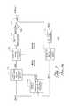
- FIG. 1illustrates the overall design of a typical amplifier system that uses predistortion to compensate for non-linearities in the amplification process.
- FIG. 2illustrates how the noise floor generated by a digital to analog converter remains constant as the signal bandwidth expands.
- FIG. 3illustrates an amplifier design in accordance with one embodiment of the invention.
- FIGS. 4A-Eillustrate how the noise floor can be lowered by separately converting signals to analog along each signal path.
- FIG. 5illustrates how extended FIR filter coefficients can be computed by utilizing an LMS subband equalizer.
- FIGS. 6A-Gillustrate a number of additional and alternative embodiments.
- FIG. 7illustrates a hardware implementation according to one embodiment.
- the North American digital cellular telephony servicesemploy linear modulation schemes to encode baseband information in both the amplitude and phase of a radio frequency (RF) carrier. This is undertaken to achieve an increase in spectral efficiency. If significant intermodulation and distortion products are to be avoided, class A linear amplifiers should be employed. These are generally inefficient and undesirable in systems where cost and heat dissipation are prohibitive factors. To avoid the compromise of constraints between the regulatory spectral emission mask and amplifier efficiency, attempts have been made to harness the efficiency of nonlinear class AB amplifiers by various digital linearization techniques. These techniques usually involve utilizing a digital to analog converter to drive the modulators in the upconversion circuitry with both the desired modulation signal and the correction signal all embedded within a single complex or real data stream.
- RFradio frequency
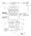
- FIG. 1illustrates the overall design of a typical amplifier system 100 that uses predistortion to compensate for non-linearities in the amplification process.
- the amplifier designincludes the following components: a Digital Compensation Signal Processing (DCSP) block 102 , a generalized digital to analog conversion (DAC) block 104 , an RF up conversion chain 106 , a nonlinear amplifier (or amplifier assembly containing multiple nonlinear amplifiers) 108 , an amplifier sampling structure (e.g., a Lange, Hybrid or Quadrature coupler) 110 , an RF down conversion chain 112 , a generalized analog to digital conversion (ADC) block, 114 and an Adaptive Control Processing and Compensation Estimator (ACPCE) block 116 .
- DCSPDigital Compensation Signal Processing
- DACdigital to analog conversion
- ADCAdaptive Control Processing and Compensation Estimator
- the basic objective of the predistorter designis to digitally compensate an input signal, Vm(t), such that after RF upconversion and amplification by a nonlinear amplifier 108 , the output of the amplifier unit is a scaled replica of the input signal, k.Vm rf (t).
- the degree of scalingis usually defined by the bulk amplifier's gain, k.
- the input signal, Vm(t)is processed by the Digital Compensation Signal Processing (DCSP) block 102 . This compensation processing is undertaken to correct for all upconversion linear imperfections and the nonlinearity of the amplifier.
- DCSPDigital Compensation Signal Processing
- the compensationis undertaken such that the output signal from the Digital Compensation Signal Processing (DCSP) block 102 , Vd(t), is distorted in a manner that is complementary, i.e., opposite in nature, to that incurred by the RF upconversion and amplification process.
- the complementary distortionis such that the composite of the distortion introduced by the Digital Compensation Signal Processing (DCSP) block 102 and by the RF upconversion and amplification processes effectively cancel each other resulting in a linearly amplified version, i.e., scaled, of the input signal Vm(t).
- the Adaptive Control Processing and Compensation Estimator (ACPCE) 116operates by capturing digital samples of the input signal Vm(t) and the output, Vf(t), of the power amplifier unit 108 . These samples are derived from the RF output signal k.Vm rf (t), via the RF power sampling coupler 110 and down conversion circuits 112 which feed an intermediate frequency (IF) or baseband analog to digital converter (ADC) 114 .
- IFintermediate frequency
- ADCanalog to digital converter
- the Adaptive Control Processing and Compensation Estimator (ACPCE) 116computes the time delay difference between digital samples of the observed amplifier output and the ideal input signal. Once this has been achieved the Adaptive Control Processing and Compensation Estimator (ACPCE) 116 can accurately determine the update adjustment, if required, that is to be made to the correction coefficients that the Digital Compensation Signal Processing (DCSP) block 102 currently utilizes. Update adjustments are provided to the DCSP via a state parameter update vector x + (t) that contains one or more sets of correction parameter updates.
- FIG. 2illustrates the aforementioned problem, where the noise floor generated by the DAC 104 remains constant as the signal bandwidth expands. As the signal bandwidth expands, the signal's subband to noise floor ratio steadily falls. This degradation causes current designs of digital linearized amplifiers, such as cartesian predistortion and digitally controlled feedforward designs, to be limited to a maximum bandwidth which currently does not exceed 5 MHz. The limitation is defined because the overall communications system requirement specifications often call for a minimum signal to noise performance ratio within any one subband. Currently, the problem is addressed by employing a single radio transceiver and amplifier for each subband.
- the present inventionovercomes the above problem by separating the wideband input signal into multiple subbands, precompensating or compensating the subbands, and then converting each subband to analog form using a subband-specific DAC.
- an analog correction signalis preferably generated by predistorting the entire wideband input signal, taking the difference between this predistorted signal and the input signal, and converting the result to analog form using still another DAC. The resulting analog signals are combined to form the input to the amplifier.
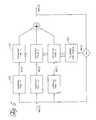
- FIG. 3illustrates an amplifier design 300 in accordance with one embodiment of the invention.
- a bank of frequency demultiplexers 320separates a wideband digital input signal Vm(t) into multiple digital subband signals, each of which falls within a different respective frequency band of Vm(t).
- FIG. 3illustrates three subbands, Vm 1 (t), Vm 2 (t), and Vm 3 (t), however, one or more subbands may be used in other embodiments.
- An embodiment in which the wideband input signal is not divided into subbandsis described separately below with reference to FIG. 6 F.
- the bank of frequency demultiplexers 320may be implemented with digital filters, such as finite impulse response (FIR) filters, infinite impulse response (IIR) filters, or quadrature mirror filters. Each filter may be designed so that the noise floor in each subband will be sufficiently low to meet the applicable system requirements.
- FIRfinite impulse response
- IIRinfinite impulse response
- Each digital subband signalis passed through a respective correction filter 322 to create a precompensated digital subband signal.
- the correction filters 322which may be FIR filters or IIR filters, are configured to correct phase, gain and delay imbalances between the individual pathways. The functionality of the correction filters 322 will be discussed in greater detail below.
- Each of the precompensated digital subband signalsis then converted to an analog subband signal using a separate digital to analog converter (DAC) 324 .
- DACdigital to analog converter
- Each analog subband signalis then passed through a reconstruction filter 326 which has a passband that is comparable to the corresponding signal's subband width.
- the digital input signalis also supplied to a digital predistortion engine 301 which creates a predistorted digital input signal Vp(t).
- the predistortion engine 301includes an amplifier sampling structure (e.g., a Lange, Hybrid or Quadrature coupler) 310 , an RF down conversion chain 312 , a generalized analog to digital conversion (ADC) block 314 , an Adaptive Control Processing and Compensation Estimator (ACPCE) block 316 , and a Digital Compensation Signal Processor (DCSP) 302 . Examples of devices and signal processing methods that may be used to implement these components, and particularly the DCSP 302 and the ACPCE 316 , are set forth in U.S. application Ser. Nos. 09/596,142, filed Jun.
- the digital input signal Vm(t)is removed from the predistorted digital input signal Vp(t) (created by the predistortion engine 301 ) to leave the difference, which is a digital correction signal Vd(t) only.
- the digital input signal Vm(t) that is removedmay be obtained directly or may be derived by summing the subband signals, as shown. Since the correction signal Vd(t) is supplied separately, a separate DAC 334 and a separate narrow band reconstruction filter 336 can be utilized to convert the correction signal. Accordingly, separate digital to analog pathways are used to convert the input signal Vm(t) (or Vm 1 (t), Vm 2 (t), and Vm 3 (t)) and the correction signal.
- the converted analog correction signal Vd(t) and the converted analog input signal Vm(t) (or its subbands)are then combined with an analog summing junction 340 to form a composite predistorted analog input signal.
- the composite signalis then passed on to an RF up conversion chain 306 and a non-linear amplifier 308 (or amplifier assembly containing multiple nonlinear amplifiers) to create an output signal k.Vm rf (t).
- the correction signal Vd(t)is usually significantly wider in bandwidth than the original input signal Vm(t) but significantly lower in power.
- the full dynamic range of the DAC in each pathwaymay be advantageously utilized to maximize the signal to noise ratio.
- a correction signal with a low powerwould have to share all of the levels of quantization of a DAC with an input signal of much higher power. Since the correction signal has a much lower power, only a relatively small number of the quantization levels of the DAC would be effectively used to convert the correction signal.
- the separate narrow band reconstruction filters 326 and 336introduce relative inconsistencies in gain, phase, and delay between the separate signals. These inconsistencies are corrected by the correction filter 322 positioned in-line along each subband signal path before the DACs.
- the correction filters 322are driven by the Adaptive Control Processing and Compensation Estimator (ACPCE) 316 , which adaptively generates compensation parameters for the filters based on observations of the input signal Vm(t) and the feedback signal, Vf(t).
- the ACPCE 316provides corrective updates to the correction filters through a state vector y + (t) to precisely match the gain, phase, and delay of the individual subband paths. This permits substantially perfect analog reconstruction of the input signal when the multiple subbands are recombined by the analog circuitry.
- the functionality of the ACPCE 316will be discussed in greater detail in the next section.
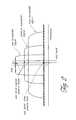
- FIGS. 4A-Eillustrate how separately converting each signal path lowers the noise floor.
- FIG. 4Ashows the noise floor to signal to noise ratio that would be achieved if the entire signal were directly fed to a single (or complex pair) DAC.
- FIG. 4Billustrates the advantage of noise floor suppression if individual DACs are utilized for each subband. The headroom of the DAC to quantization noise floor is maximized for each subband. As a result, the inband signal to noise ratio is maximized while the utilization of tight reconstruction filters permits the out of band or wideband noise floor to be reduced by the roll-off of the reconstruction filters.
- An individual subband contributoris illustrated in FIG. 4 C.
- FIG. 4Dillustrates the Power Spectral Density (PSD) of the correction signal Vd(t).
- the correction signalexhibits a lower signal to noise ratio because the signal is by nature a wideband correction signal.
- the noise flooris not ordinarily of concern, however, since the signal is normally 30 to 40 dB lower than the main signal.
- the wideband noise flooris significantly lower than that of the composite signal and corrective action to lower this component's noise floor is not necessary.
- FIG. 4Eillustrates a composite signal including the correction signal Vd(t) and the information bearing signal Vm(t). In the composite signal, the noise floor is significantly lower because the correction signal contribution is significantly lower in power when compared to the main input signal.
- an adaption predistortion kernelwhich is a configuration of the predistortion engine 301, operates in accordance with the above-referenced wideband applications. Specifically, the ACPCE captures the input signal, Vm(t), and the feedback observational signal, Vf(t), and adaptively computes DCSP predistortion correction coefficients that, when downloaded to the DCSP, will predistort the input signal to eliminate a difference between the amplifier's output signal and the input signal.
- the input signal (decomposed into sub-bands) and the predistortion correction signalare linearly combined in the analog signal processing domain. Due to the imperfections of the analog circuitry, the recombining process is subject to a variety of errors. Specifically, gain, phase, delay, and group delay variations between the independent analog pathways can undermine the efficacy of the predistortion process. These effects can be eliminated using the correction FIR filters. To ensure that recombination occurs in an error free manner, the following analog linear imperfections should be eliminated:
- Correction coefficients to eliminate these effectsare easily computed by the addition of a few simple algorithms to the existing algorithm set as set forth in the wideband applications.
- the result of these new simple algorithms when executed by the ACPCEwill be a set of linear correction FIR filter coefficients that are downloaded from the ACPCE to the correction filters to simply balance each subband signal with respect to the others and the predistortion correction signal pathway.
- Equation (1)The output of the analog subband recombination process may be described by Equation (1):
- Vm a ( t )⁇ 1 e j ⁇ 1 ( ⁇ ( t+ ⁇ 1 ) ⁇ circle around ( ⁇ ) ⁇ h 1 ( t ) ⁇ circle around ( ⁇ ) ⁇ V 1 ( t ))+ ⁇ 2 e j ⁇ 2 ( ⁇ ( t+ ⁇ 2 ) ⁇ circle around ( ⁇ ) ⁇ h 2 ( t ) ⁇ circle around ( ⁇ ) ⁇ V 2 ( t ))+. . .
- Vm a (t)represents the analog recombination of Vm(t) the input signal and ⁇ , ⁇ , ⁇ and h(t) are the independent analog gain, phase, delay and impulse response of the individual analog subband pathways. Assuming that no loss of signal information occurs in the process of creating subbands, then ideally Equation (2) holds.
- each of the independent gain, phase, and delay differencesare estimated and corrected so that the recombination process is accurate and faithfully regenerates the input signal Vm(t). This is achieved very easily by performing a simple correlation between each subband component and the observed feedback signal.
- the correction filter coefficients for each subbandare readily identified from the resulting individual correlation peaks. Each peak identifies the bulk gain, phase, and delay incurred by each subband. When provided with this information, it is a simple and direct computation to compute the coefficients of a FIR filter that equalize these differences between each subband pathway. Once this has been achieved by the ACPCE, the correct coefficients can be downloaded to the correction FIR filters 322 .
- the gain, phase, and bulk delay of the predistortion correction pathwaycan be readily identified or estimated by a simple correlation.
- This particular estimationhas a fairly wide tolerance. Provided that the estimation falls within ninety degrees of phase and the overall absolute delay is matched to the subband pathways within the span of the predistortion engine's memory kernel, the normal predistortion adaption algorithm will immediately respond and correct any residual estimation error by compensating within the DCSP coefficients.
- Initial estimates of the correctioncan be formulated by applying a bulk gain, phase and delay shift equally to all sub-band correction coefficients to ensure that the recombined input signal is aligned with the predistortion correction signal.
- the correctioncan be convolved into the normal starting conditions of the adaption kernel. For simplicity, the foremost option is usually preferred.
- Subsection A abovediscusses the elimination of the bulk gain, phase and delay differences between the individual subband signal pathways, however group delay variations between the individual reconstruction filters utilized in the analog domain will also adversely affect the recombination process and eventually the predistortion process. These effects can also be readily eliminated through the correction FIR filter structure.
- LMSleast mean squares
- N tapsO taps + ⁇ V e V d (3)
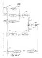
- FIG. 6Aillustrates an extension to the design that permits RF combining as opposed to low IF or baseband combining to be utilized. This approach also permits suppression of wideband phase noise by the upconvertor filtering in addition to wideband quantization effects. Also illustrated in FIG. 6A is a configuration in which the digital input signal Vm(t) is supplied directly to the predistortion engine 301 .
- the designcan be extended to utilize an individual upconversion and modulation process for each subband signal.
- the input wideband signalmay not exercise all subbands yet each subband may be subject to data flow on a moments notice.
- the RF components and analog baseband componentscan drift. Accurate tracking of these changes can be accomplished by injecting antiphase sequences either during transmission or non-transmission events.
- Antiphase sequencesare specially designed sequences that cancel prior to PA amplification in perfectly balanced signal processing chains, as set forth in U.S. Pat. No. 5,990,734, the disclosure of which is hereby incorporated by reference. If perfect balance is not exhibited, the ACPCE is provided with immediate error information in the feedback signal to rectify the situation.
- FIG. 6 CA complex quad mod design is shown in FIG. 6 C.
- the design in FIG. 6Cincludes a quadrature modulator 632 and a quadrature demodulator 634 .
- FIG. 6Dillustrates a design where digital synthesizers (DDS) 642 are utilized to assist in the construction of a single composite wideband signal that is fed to the subband filter bank which then demultiplexes the wideband signal in accordance with the previously described mode of operation.
- FIG. 6Eillustrates a further variation where a routing multiplexer (mux) 652 is utilized to form the individual subbands rather than a filter bank.
- DDSdigital synthesizers
- Another extension that can extend the design's overall operating bandwidthis to use a further modification to the predistortion architecture that permits the correction signal's bandwidth to be minimized.
- the predistortion engineis utilized to create an identical distortion signal to that created by the main amplifier 308 . This signal is then subtracted from the main amplifier's output signal.
- the approachworks because in ultra wideband designs the normal “inverted” correction signal occupies about 7 to 11 times the input signal bandwidth. This approach permits the corrective action to occupy a bandwidth that is only about 3 to 5 times the input signal bandwidth.
- the downsideis that the additional amplifier tends to reduce system efficiency.
- FIG. 6Fillustrates a lower cost embodiment of the invention that trades a reduction in overall noise suppression performance against the number of DACs that are actually used.
- the upper data pathwayis constructed utilizing a correction FIR filter 322 that permits the input signal to be passed directly to the output DACs 314 .
- the bandwidth used by the reconstruction filters 326 along this pathis tight and strictly limited directly to the input signal Vm(t) or composite signal's bandwidth.
- the second pathwayis utilized by the predistortion engine 301 to supply a wide bandwidth predistortion signal Vp(t) but lower power signal to the external analog summing junction 340 .
- the reconstruction filter 336 in this scenariois defined by the predistortion signal's bandwidth, which is ordinarily wider than the input signal bandwidth by a factor of about three to nine.
- This cost reduced embodimentcan be utilized in all of the aforementioned configurations including baseband, IF or RF combining with direct conversion, or digital IF configurations.
- FIG. 6Gillustrates a configuration in which the ACPCE creates the state vector y + (t) (used to configure the correction filters) based upon the reconstructed and combined input signal Vm(t) rather than the amplifier output k.Vm rf (t).
- the reconstructed and combined input signalis passed through an ADC 672 and then on to the ACPCE 316 .
- the digital input signal Vm(t)may be supplied directly to the predistortion engine 301 rather than using a combination of the subbands.
- FIG. 7illustrates an example circuit 700 , which may be used to implement the above-described embodiments of the invention.
- a DCSP core 702preferably includes wideband predistortion architecture, frequency subband demultiplexers, multiple DAC drivers, and a control interface. Due to the fast signal processing requirements of the DCSP 302 , the DCSP core is preferably implemented using dedicated hardware such as a field programmable gate array (FPGA) or dedicated silicon in an ASIC. The ASIC or FPGA may need a modest amount of ‘glue logic’ 704 to interface the DCSP to a standard microprocessor or DSP 710 that implements the ACPCE 316 , which computes and delivers updated DCSP coefficients.
- FPGAfield programmable gate array
- the ACPCE 316preferably operates in non-real time such that a general purpose DSP or microprocessor 710 may be used, such as a TMS320C54, a TMS320C60, a TMS320C40, an ARM 7, or a Motorola 68000.
- This processor 710is preferably augmented with non-volatile ROM 712 for both program storage and factory installed default parameters. Both ROM 712 and Flash ROM 714 are particularly suitable for this purpose.
- a proportional amount of RAM 716is used for general purpose program execution.
- the DCSP core 702can also provide an interface to a data storage RAM 704 where sets of observed amplifier input signal sequences may be stored prior to utilization by the ACPCE.
- This RAM 704may reside on the ASIC chip.
- the ACPCEprovides updated and/or adapted compensation parameters to the DCSP core 702 on a regular basis through the RAM structure 704 .
- a separate RAM structuremay be used for this purpose.
- the DCSPis provided fast access to the compensation parameters through this RAM structure. As digital signal processors evolve in speed, the DCSP process may be performed by a processor such as a TMS320C60 from Texas Instruments or a SHARC processor from Analog Devices.
- a direct conversion up conversion baseband to RF conversionis utilized combined with a RF to IF down conversion which is appropriately sampled to capture IF data and followed by a digital quadrature conversion to complex baseband.
- this embodimentcould readily utilize direct conversion for both RF up and down conversion or utilize digital to IF conversion followed by IF to RF and vice versa for the frequency translation process.
- This inventionis applicable to any digital linearized amplifier technology. Predistortion is utilized here as an exemplary design, and is not intended to limit the scope of the invention. Application to Cartesian, and digital linearized feedforward designs is possible. The approach permits digital amplifier designs to evolve which permit bandlimited wideband RF signals, optical signals or IF signals to be successfully amplified. The invention can be used for multiple signals and for any modulation scheme or combination of modulations. Where multiple signals are amplified they can each have any modulation type.
Landscapes
- Physics & Mathematics (AREA)
- Nonlinear Science (AREA)
- Engineering & Computer Science (AREA)
- Power Engineering (AREA)
- Amplifiers (AREA)
Abstract
Description

Claims (32)
Priority Applications (1)
| Application Number | Priority Date | Filing Date | Title |
|---|---|---|---|
| US09/770,568US6570444B2 (en) | 2000-01-26 | 2001-01-26 | Low noise wideband digital predistortion amplifier |
Applications Claiming Priority (2)
| Application Number | Priority Date | Filing Date | Title |
|---|---|---|---|
| US17822300P | 2000-01-26 | 2000-01-26 | |
| US09/770,568US6570444B2 (en) | 2000-01-26 | 2001-01-26 | Low noise wideband digital predistortion amplifier |
Publications (2)
| Publication Number | Publication Date |
|---|---|
| US20010054974A1 US20010054974A1 (en) | 2001-12-27 |
| US6570444B2true US6570444B2 (en) | 2003-05-27 |
Family
ID=26874113
Family Applications (1)
| Application Number | Title | Priority Date | Filing Date |
|---|---|---|---|
| US09/770,568Expired - LifetimeUS6570444B2 (en) | 2000-01-26 | 2001-01-26 | Low noise wideband digital predistortion amplifier |
Country Status (1)
| Country | Link |
|---|---|
| US (1) | US6570444B2 (en) |
Cited By (57)
| Publication number | Priority date | Publication date | Assignee | Title |
|---|---|---|---|---|
| US20020027958A1 (en)* | 2000-06-22 | 2002-03-07 | Kolanek James C. | Feedback channel signal recovery |
| US20020113905A1 (en)* | 2000-12-28 | 2002-08-22 | Lg Electronics Inc. | Linearization compensation system of digital TV relay apparatus and method thereof |
| US20040027198A1 (en)* | 2002-08-09 | 2004-02-12 | Andrew Corporation, A Delaware Corporation | Linearizing LINC amplifiers using pre-distortion |
| US20040047285A1 (en)* | 2002-09-11 | 2004-03-11 | Foerster Jeffrey R. | Sub-banded ultra-wideband communications system |
| US20040105510A1 (en)* | 2002-12-03 | 2004-06-03 | Motorola, Inc. | Digital predistortion system for linearizing a power amplifier |
| US20040160933A1 (en)* | 2003-02-18 | 2004-08-19 | Odenwalder Joseph P. | Code division multiplexing commands on a code division multiplexed channel |
| US6785342B1 (en)* | 2000-11-06 | 2004-08-31 | Wideband Semiconductors, Inc. | Nonlinear pre-distortion modulator and long loop control |
| US20040228283A1 (en)* | 2003-05-14 | 2004-11-18 | Naguib Ayman Fawzy | Power control and scheduling in an OFDM system |
| US20040228389A1 (en)* | 2003-03-06 | 2004-11-18 | Odenwalder Joseph P. | Systems and methods for using code space in spread-spectrum communications |
| US20040232953A1 (en)* | 2003-02-28 | 2004-11-25 | Infineon Technologies Ag | Line driver |
| US20040252786A1 (en)* | 2003-06-10 | 2004-12-16 | Mchenry Mark Allen | Method and system for transmitting signals with reduced spurious emissions |
| US20050003843A1 (en)* | 2003-02-18 | 2005-01-06 | Ho Sai Yiu Duncan | System and method for scheduling transmissions in a wireless communication system |
| US20050002324A1 (en)* | 2003-05-14 | 2005-01-06 | Arak Sutivong | Interference and noise estimation in an OFDM system |
| US20050221760A1 (en)* | 2004-03-31 | 2005-10-06 | Tinsley Keith R | Pulse shaping signals for ultrawideband communication |
| US20060056536A1 (en)* | 2004-09-10 | 2006-03-16 | Kazuyuki Hori | Delay locked loop circuit, digital predistortion type transmitter using same, and wireless base station |
| US20060109052A1 (en)* | 2003-07-03 | 2006-05-25 | Aryan Saed | Adaptive predistortion for a transmit system |
| WO2005091865A3 (en)* | 2004-03-03 | 2007-06-14 | Powerwave Technologies Inc | Digital predistortion system and method for high efficiency trasmitters |
| US20080082597A1 (en)* | 2006-09-29 | 2008-04-03 | Optichron, Inc. | Low power and low complexity adaptive self-linearization |
| US20080163334A1 (en)* | 2006-12-29 | 2008-07-03 | Filip Perich | Method and device for policy-based control of radio |
| US20080194286A1 (en)* | 2003-02-18 | 2008-08-14 | Qualcomm Incorporated | Systems and methods for performing outer loop power control in wireless communication systems |
| US20080211576A1 (en)* | 2007-02-26 | 2008-09-04 | Harris Corporation | Linearization of RF Power Amplifiers Using an Adaptive Subband Predistorter |
| US20080270082A1 (en)* | 2006-09-29 | 2008-10-30 | Optichron, Inc. | Low-power and low-cost adaptive self-linearization system with fast convergence |
| US20080288199A1 (en)* | 2006-09-29 | 2008-11-20 | Optichron, Inc. | Distortion cancellation using adaptive linearization |
| US20090047920A1 (en)* | 2007-08-15 | 2009-02-19 | Shared Spectrum Company | Methods for detecting and classifying signals transmitted over a radio frequency spectrum |
| US20090112579A1 (en)* | 2007-10-24 | 2009-04-30 | Qnx Software Systems (Wavemakers), Inc. | Speech enhancement through partial speech reconstruction |
| US20090251211A1 (en)* | 2008-04-02 | 2009-10-08 | Harris Corporation | Feedforward linearization of rf power amplifiers |
| US20090268619A1 (en)* | 2007-08-15 | 2009-10-29 | Shared Spectrum Company | Systems and methods for a cognitive radio having adaptable characteristics |
| US20090292536A1 (en)* | 2007-10-24 | 2009-11-26 | Hetherington Phillip A | Speech enhancement with minimum gating |
| US20100008313A1 (en)* | 2006-05-12 | 2010-01-14 | Shared Spectrum Company | Method and System for Determining Spectrum Availability Within a Network |
| US20100075704A1 (en)* | 2008-08-19 | 2010-03-25 | Shared Spectrum Company | Method and System for Dynamic Spectrum Access Using Specialty Detectors and Improved Networking |
| US20100097952A1 (en)* | 2006-05-12 | 2010-04-22 | Shared Spectrum Company | Method and System for Classifying Communication Signals in a Dynamic Spectrum Access System |
| US20100105332A1 (en)* | 2006-05-12 | 2010-04-29 | Shared Spectrum Company | Method and System for Dynamic Spectrum Access Using Detection Periods |
| US20100173586A1 (en)* | 2006-05-12 | 2010-07-08 | Shared Spectrum Company | Method and System for Dynamic Spectrum Access |
| US20100308910A1 (en)* | 2009-06-04 | 2010-12-09 | Xilinx, Inc. | Apparatus and method for predictive over-drive detection |
| US8023950B2 (en) | 2003-02-18 | 2011-09-20 | Qualcomm Incorporated | Systems and methods for using selectable frame durations in a wireless communication system |
| US8023588B1 (en) | 2008-04-08 | 2011-09-20 | Pmc-Sierra, Inc. | Adaptive predistortion of non-linear amplifiers with burst data |
| US8027249B2 (en) | 2006-10-18 | 2011-09-27 | Shared Spectrum Company | Methods for using a detector to monitor and detect channel occupancy |
| US8081598B2 (en) | 2003-02-18 | 2011-12-20 | Qualcomm Incorporated | Outer-loop power control for wireless communication systems |
| USRE43066E1 (en) | 2000-06-13 | 2012-01-03 | Shared Spectrum Company | System and method for reuse of communications spectrum for fixed and mobile applications with efficient method to mitigate interference |
| US8201039B2 (en) | 2003-08-05 | 2012-06-12 | Qualcomm Incorporated | Combining grant, acknowledgement, and rate control commands |
| US20120157017A1 (en)* | 2008-02-11 | 2012-06-21 | Broadcom Corporation | Rf transmitter and integrated circuit with programmable baseband filtering and methods for use therewith |
| US8326616B2 (en) | 2007-10-24 | 2012-12-04 | Qnx Software Systems Limited | Dynamic noise reduction using linear model fitting |
| US8526966B2 (en) | 2003-02-18 | 2013-09-03 | Qualcomm Incorporated | Scheduled and autonomous transmission and acknowledgement |
| US8548387B2 (en) | 2003-03-06 | 2013-10-01 | Qualcomm Incorporated | Method and apparatus for providing uplink signal-to-noise ratio (SNR) estimation in a wireless communication system |
| US8660207B2 (en) | 2011-05-12 | 2014-02-25 | Andrew Llc | Digital pre-distortion with carrier cancellation |
| US8699452B2 (en) | 2003-02-18 | 2014-04-15 | Qualcomm Incorporated | Congestion control in a wireless data network |
| US8824980B2 (en)* | 2012-09-05 | 2014-09-02 | Analog Devices, Inc. | System and method to implement a radio transmitter with digital predistortion having reduced noise |
| US8837633B2 (en) | 2011-10-21 | 2014-09-16 | Xilinx, Inc. | Systems and methods for digital processing based on active signal channels of a communication system |
| US8842033B1 (en) | 2013-09-30 | 2014-09-23 | Agilent Technologies, Inc. | Dynamic linearity corrector for digital-to-analog converters |
| US8903346B2 (en) | 2011-03-28 | 2014-12-02 | Adc Telecommunications, Inc. | External mounted amplifiers with active interference cancelation using diversity antennas |
| US9712193B1 (en) | 2016-04-12 | 2017-07-18 | Cisco Technology, Inc. | High power efficient amplifier through digital pre-distortion and machine learning in cable network environments |
| US9735814B1 (en) | 2016-04-12 | 2017-08-15 | Cisco Technology, Inc. | High power efficient amplification at cable modems through digital pre-distortion and machine learning in cable network environments |
| US9735741B2 (en) | 2014-08-28 | 2017-08-15 | Analog Devices Global | Receivers for digital predistortion |
| US9787335B1 (en)* | 2016-05-23 | 2017-10-10 | Kmw Inc. | Method and apparatus for determining validity of samples for digital pre-distortion apparatus |
| US9998379B2 (en) | 2003-02-18 | 2018-06-12 | Qualcomm Incorporated | Method and apparatus for controlling data rate of a reverse link in a communication system |
| US10797750B2 (en) | 2016-02-24 | 2020-10-06 | Cisco Technology, Inc. | System architecture for supporting digital pre-distortion and full duplex in cable network environments |
| US11038474B2 (en) | 2017-11-01 | 2021-06-15 | Analog Devices Global Unlimited Company | Phased array amplifier linearization |
Families Citing this family (39)
| Publication number | Priority date | Publication date | Assignee | Title |
|---|---|---|---|---|
| US7924937B2 (en) | 2002-03-04 | 2011-04-12 | Stmicroelectronics N.V. | Resonant power converter for radio frequency transmission and method |
| AU2003217890A1 (en)* | 2002-03-04 | 2003-09-22 | Stmicroelectronics, N.V. | Coder apparatus for resonant power conversion and method |
| US6975167B2 (en) | 2003-07-03 | 2005-12-13 | Icefyre Semiconductor Corporation | Adaptive predistortion for a transmit system with gain, phase and delay adjustments |
| US7409193B2 (en)* | 2003-07-03 | 2008-08-05 | Zarbana Digital Fund Llc | Predistortion circuit for a transmit system |
| US7453952B2 (en)* | 2003-07-03 | 2008-11-18 | Saed Aryan | Predistortion circuit for a transmit system |
| US7026871B2 (en)* | 2003-07-03 | 2006-04-11 | Icefyre Semiconductor, Inc. | Adaptive predistortion for a transmit system |
| US7366252B2 (en)* | 2004-01-21 | 2008-04-29 | Powerwave Technologies, Inc. | Wideband enhanced digital injection predistortion system and method |
| US7995490B2 (en)* | 2004-06-29 | 2011-08-09 | Spirent Communications, Inc. | System and method for identifying a signature of a device, in a communication circuit, utilizing distortion products |
| US7933942B2 (en)* | 2006-09-29 | 2011-04-26 | Teradyne, Inc. | Low cost, high purity sign wave generator |
| US8904560B2 (en) | 2007-05-07 | 2014-12-02 | Bruker Nano, Inc. | Closed loop controller and method for fast scanning probe microscopy |
| US8345727B2 (en)* | 2008-05-13 | 2013-01-01 | Metropolitan Area Networks, Inc. | Communication system, apparatus, and methods |
| US8081936B2 (en) | 2009-01-22 | 2011-12-20 | Mediatek Inc. | Method for tuning a digital compensation filter within a transmitter, and associated digital compensation filter and associated calibration circuit |
| WO2010083588A1 (en) | 2009-01-23 | 2010-07-29 | Nortel Networks Limited | High speed signal generator |
| US7859439B2 (en)* | 2009-04-07 | 2010-12-28 | Mediatek Inc. | Processing apparatus for calibrating analog filter according to frequency-related characteristic of analog filter, processing apparatus for generating compensation parameter used to calibrate analog filter, related communication device, and methods thereof |
| CA2729645C (en)* | 2010-02-02 | 2014-11-04 | Vecima Networks Inc. | Multiple reduced-bandwidth processing paths to achieve a full and continuous output band for multiple-channel catv upconversion |
| US9184756B2 (en)* | 2010-11-08 | 2015-11-10 | Analog Devices, Inc. | Variable dynamic range receiver |
| CN102299878B (en)* | 2011-09-06 | 2014-03-19 | 电信科学技术研究院 | Method and device for realizing multi-band digital predistortion (DPD) |
| US8576943B2 (en)* | 2011-09-09 | 2013-11-05 | Telefonaktiebolaget L M Ericsson (Publ) | Linearization for a single power amplifier in a multi-band transmitter |
| US20140029683A1 (en)* | 2012-07-26 | 2014-01-30 | Telefonaktiebolaget L M Ericsson (Publ) | Multi-Band Observation Receiver |
| WO2014092617A1 (en)* | 2012-12-13 | 2014-06-19 | Telefonaktiebolaget L M Ericsson (Publ) | Digital pre-distortion for high bandwidth signals |
| US9007250B1 (en)* | 2013-10-22 | 2015-04-14 | L-3 Communications Corp. | Time-interleaved and sub-band reconstruction approaches to digital-to-analog conversion for high sample rate waveform generation |
| US9967027B2 (en)* | 2016-07-14 | 2018-05-08 | Cisco Technology, Inc. | Optical transceiver compensation, monitoring and alarming |
| CN109428625B (en)* | 2017-08-24 | 2020-12-04 | 大唐移动通信设备有限公司 | Cell signal merging transmission method and device |
| US10917074B2 (en)* | 2019-03-29 | 2021-02-09 | Bose Corporation | Subband adaptive filter for systems with partially acausal transfer functions |
| JP7297549B2 (en)* | 2019-06-21 | 2023-06-26 | エイブリック株式会社 | VOLTAGE-CURRENT CONVERSION CIRCUIT AND CHARGE/DISCHARGE CONTROL DEVICE |
| US11025358B1 (en) | 2020-04-20 | 2021-06-01 | Bae Systems Information And Electronic Systems Integration Inc. | Method of adaptively mitigating common template multi-channel wireless interference |
| US11394414B2 (en)* | 2020-04-20 | 2022-07-19 | Bae Systems Information And Electronic Systems Integration Inc. | Method of wireless interference mitigation with efficient utilization of computational resources |
| US11451329B2 (en)* | 2021-01-25 | 2022-09-20 | Huawei Technologies Co., Ltd. | Method and apparatus of low-complexity pattern dependent lookup table pre-compensation |
| US12231088B2 (en) | 2021-06-18 | 2025-02-18 | Qorvo Us, Inc. | Wideband transmission circuit |
| US12199577B2 (en) | 2021-06-18 | 2025-01-14 | Qorvo Us, Inc. | Envelope tracking voltage correction in a transmission circuit |
| US12206365B2 (en) | 2021-06-18 | 2025-01-21 | Qorvo Us, Inc. | Voltage ripple suppression in a transmission circuit |
| US12401332B2 (en) | 2021-09-16 | 2025-08-26 | Qorvo Us, Inc. | Phase and amplitude error correction in a transmission circuit |
| US12323174B2 (en)* | 2021-09-16 | 2025-06-03 | Qorvo Us, Inc. | Amplitude-to-phase error correction in a transceiver circuit |
| US12284003B2 (en) | 2021-09-16 | 2025-04-22 | Qorvo Us, Inc. | Phase and amplitude error correction in a transmission circuit |
| US12273081B2 (en) | 2022-01-27 | 2025-04-08 | Qorvo Us, Inc. | Voltage ripple reduction in a power management circuit |
| US12381525B2 (en) | 2022-06-28 | 2025-08-05 | Qorvo Us, Inc. | Amplifier system |
| GB2624195A (en)* | 2022-11-09 | 2024-05-15 | Qinetiq Ltd | Signal processor |
| WO2024239223A1 (en)* | 2023-05-23 | 2024-11-28 | Nokia Shanghai Bell Co., Ltd. | Apparatuses for communication |
| WO2025040264A1 (en)* | 2023-08-24 | 2025-02-27 | Telefonaktiebolaget Lm Ericsson (Publ) | Methods and apparatuses for performing quantisation noise suppression |
Citations (8)
| Publication number | Priority date | Publication date | Assignee | Title |
|---|---|---|---|---|
| US4291277A (en)* | 1979-05-16 | 1981-09-22 | Harris Corporation | Adaptive predistortion technique for linearizing a power amplifier for digital data systems |
| US5699383A (en)* | 1995-03-06 | 1997-12-16 | Nec Corporation | High-power linear amplification using periodically updated amplitude and phase correction values |
| US5748678A (en)* | 1995-07-13 | 1998-05-05 | Motorola, Inc. | Radio communications apparatus |
| US5825829A (en)* | 1995-06-30 | 1998-10-20 | Scientific-Atlanta, Inc. | Modulator for a broadband communications system |
| US5959499A (en)* | 1997-09-30 | 1999-09-28 | Motorola, Inc. | Predistortion system and method using analog feedback loop for look-up table training |
| US6091941A (en)* | 1995-09-19 | 2000-07-18 | Fujitsu Limited | Radio apparatus |
| US6240144B1 (en)* | 1998-08-06 | 2001-05-29 | Samsung Electronics Co., Ltd. | Apparatus and method of linearizing a power amplifier in a mobile radio communication system |
| US6304596B1 (en)* | 1997-05-09 | 2001-10-16 | Broadcom Homenetworking, Inc. | Method and apparatus for reducing signal processing requirements for transmitting packet-based data with a modem |
- 2001
- 2001-01-26USUS09/770,568patent/US6570444B2/ennot_activeExpired - Lifetime
Patent Citations (8)
| Publication number | Priority date | Publication date | Assignee | Title |
|---|---|---|---|---|
| US4291277A (en)* | 1979-05-16 | 1981-09-22 | Harris Corporation | Adaptive predistortion technique for linearizing a power amplifier for digital data systems |
| US5699383A (en)* | 1995-03-06 | 1997-12-16 | Nec Corporation | High-power linear amplification using periodically updated amplitude and phase correction values |
| US5825829A (en)* | 1995-06-30 | 1998-10-20 | Scientific-Atlanta, Inc. | Modulator for a broadband communications system |
| US5748678A (en)* | 1995-07-13 | 1998-05-05 | Motorola, Inc. | Radio communications apparatus |
| US6091941A (en)* | 1995-09-19 | 2000-07-18 | Fujitsu Limited | Radio apparatus |
| US6304596B1 (en)* | 1997-05-09 | 2001-10-16 | Broadcom Homenetworking, Inc. | Method and apparatus for reducing signal processing requirements for transmitting packet-based data with a modem |
| US5959499A (en)* | 1997-09-30 | 1999-09-28 | Motorola, Inc. | Predistortion system and method using analog feedback loop for look-up table training |
| US6240144B1 (en)* | 1998-08-06 | 2001-05-29 | Samsung Electronics Co., Ltd. | Apparatus and method of linearizing a power amplifier in a mobile radio communication system |
Cited By (121)
| Publication number | Priority date | Publication date | Assignee | Title |
|---|---|---|---|---|
| USRE43066E1 (en) | 2000-06-13 | 2012-01-03 | Shared Spectrum Company | System and method for reuse of communications spectrum for fixed and mobile applications with efficient method to mitigate interference |
| USRE44492E1 (en) | 2000-06-13 | 2013-09-10 | Shared Spectrum Company | System and method for reuse of communications spectrum for fixed and mobile applications with efficient method to mitigate interference |
| USRE44237E1 (en) | 2000-06-13 | 2013-05-21 | Shared Spectrum Company | System and method for reuse of communications spectrum for fixed and mobile applications with efficient method to mitigate interference |
| USRE46905E1 (en) | 2000-06-13 | 2018-06-19 | Shared Spectrum Company | System and method for reuse of communications spectrum for fixed and mobile applications with efficient method to mitigate interference |
| USRE47120E1 (en) | 2000-06-13 | 2018-11-06 | Shared Spectrum Company | System and method for reuse of communications spectrum for fixed and mobile applications with efficient method to mitigate interference |
| US20020027958A1 (en)* | 2000-06-22 | 2002-03-07 | Kolanek James C. | Feedback channel signal recovery |
| US6785342B1 (en)* | 2000-11-06 | 2004-08-31 | Wideband Semiconductors, Inc. | Nonlinear pre-distortion modulator and long loop control |
| US20020113905A1 (en)* | 2000-12-28 | 2002-08-22 | Lg Electronics Inc. | Linearization compensation system of digital TV relay apparatus and method thereof |
| US6917389B2 (en)* | 2000-12-28 | 2005-07-12 | Lg Electronics Inc. | Linearization compensation system of digital TV relay apparatus and method thereof |
| US6930547B2 (en) | 2002-08-09 | 2005-08-16 | Andrew Corporation | Linearizing LINC amplifiers using pre-distortion |
| US20040027198A1 (en)* | 2002-08-09 | 2004-02-12 | Andrew Corporation, A Delaware Corporation | Linearizing LINC amplifiers using pre-distortion |
| US7532564B2 (en)* | 2002-09-11 | 2009-05-12 | Intel Corporation | Sub-banded ultra-wideband communications systems |
| US20040047285A1 (en)* | 2002-09-11 | 2004-03-11 | Foerster Jeffrey R. | Sub-banded ultra-wideband communications system |
| US6937669B2 (en)* | 2002-12-03 | 2005-08-30 | Motorola, Inc. | Digital predistortion system for linearizing a power amplifier |
| WO2004051844A3 (en)* | 2002-12-03 | 2004-11-25 | Motorola Inc | Digital predistortion system for linearizing a power amplifier |
| US20040105510A1 (en)* | 2002-12-03 | 2004-06-03 | Motorola, Inc. | Digital predistortion system for linearizing a power amplifier |
| US8081598B2 (en) | 2003-02-18 | 2011-12-20 | Qualcomm Incorporated | Outer-loop power control for wireless communication systems |
| US20080194286A1 (en)* | 2003-02-18 | 2008-08-14 | Qualcomm Incorporated | Systems and methods for performing outer loop power control in wireless communication systems |
| US8391249B2 (en) | 2003-02-18 | 2013-03-05 | Qualcomm Incorporated | Code division multiplexing commands on a code division multiplexed channel |
| US20040160933A1 (en)* | 2003-02-18 | 2004-08-19 | Odenwalder Joseph P. | Code division multiplexing commands on a code division multiplexed channel |
| US8699452B2 (en) | 2003-02-18 | 2014-04-15 | Qualcomm Incorporated | Congestion control in a wireless data network |
| US8526966B2 (en) | 2003-02-18 | 2013-09-03 | Qualcomm Incorporated | Scheduled and autonomous transmission and acknowledgement |
| US8150407B2 (en) | 2003-02-18 | 2012-04-03 | Qualcomm Incorporated | System and method for scheduling transmissions in a wireless communication system |
| US8023950B2 (en) | 2003-02-18 | 2011-09-20 | Qualcomm Incorporated | Systems and methods for using selectable frame durations in a wireless communication system |
| US9998379B2 (en) | 2003-02-18 | 2018-06-12 | Qualcomm Incorporated | Method and apparatus for controlling data rate of a reverse link in a communication system |
| US8977283B2 (en) | 2003-02-18 | 2015-03-10 | Qualcomm Incorporated | Scheduled and autonomous transmission and acknowledgement |
| US20050003843A1 (en)* | 2003-02-18 | 2005-01-06 | Ho Sai Yiu Duncan | System and method for scheduling transmissions in a wireless communication system |
| US20040232953A1 (en)* | 2003-02-28 | 2004-11-25 | Infineon Technologies Ag | Line driver |
| US7084677B2 (en)* | 2003-02-28 | 2006-08-01 | Infineon Technologies Ag | Line driver |
| US8576894B2 (en) | 2003-03-06 | 2013-11-05 | Qualcomm Incorporated | Systems and methods for using code space in spread-spectrum communications |
| US8548387B2 (en) | 2003-03-06 | 2013-10-01 | Qualcomm Incorporated | Method and apparatus for providing uplink signal-to-noise ratio (SNR) estimation in a wireless communication system |
| US8705588B2 (en) | 2003-03-06 | 2014-04-22 | Qualcomm Incorporated | Systems and methods for using code space in spread-spectrum communications |
| US20040228389A1 (en)* | 2003-03-06 | 2004-11-18 | Odenwalder Joseph P. | Systems and methods for using code space in spread-spectrum communications |
| US8676128B2 (en) | 2003-03-06 | 2014-03-18 | Qualcomm Incorporated | Method and apparatus for providing uplink signal-to-noise ratio (SNR) estimation in a wireless communication system |
| US20050002324A1 (en)* | 2003-05-14 | 2005-01-06 | Arak Sutivong | Interference and noise estimation in an OFDM system |
| US7012912B2 (en)* | 2003-05-14 | 2006-03-14 | Qualcomm Incorporated | Power control and scheduling in an OFDM system |
| US20040228283A1 (en)* | 2003-05-14 | 2004-11-18 | Naguib Ayman Fawzy | Power control and scheduling in an OFDM system |
| WO2004105294A3 (en)* | 2003-05-14 | 2005-04-28 | Qualcomm Inc | Power control and scheduling in an ofdm system |
| US8477592B2 (en) | 2003-05-14 | 2013-07-02 | Qualcomm Incorporated | Interference and noise estimation in an OFDM system |
| US7409010B2 (en)* | 2003-06-10 | 2008-08-05 | Shared Spectrum Company | Method and system for transmitting signals with reduced spurious emissions |
| US20090052572A1 (en)* | 2003-06-10 | 2009-02-26 | Shared Spectrum Company | Method and System for Transmitting Signals with Reduced Spurious Emissions |
| US20040252786A1 (en)* | 2003-06-10 | 2004-12-16 | Mchenry Mark Allen | Method and system for transmitting signals with reduced spurious emissions |
| US8184678B2 (en) | 2003-06-10 | 2012-05-22 | Shared Spectrum Company | Method and system for transmitting signals with reduced spurious emissions |
| US7236052B2 (en) | 2003-07-03 | 2007-06-26 | Zarbana Digital Fund, Llc | Adaptive predistortion for a transmit system |
| US20060109052A1 (en)* | 2003-07-03 | 2006-05-25 | Aryan Saed | Adaptive predistortion for a transmit system |
| US8201039B2 (en) | 2003-08-05 | 2012-06-12 | Qualcomm Incorporated | Combining grant, acknowledgement, and rate control commands |
| US8489949B2 (en) | 2003-08-05 | 2013-07-16 | Qualcomm Incorporated | Combining grant, acknowledgement, and rate control commands |
| WO2005091865A3 (en)* | 2004-03-03 | 2007-06-14 | Powerwave Technologies Inc | Digital predistortion system and method for high efficiency trasmitters |
| CN101156159B (en)* | 2004-03-03 | 2010-09-01 | 电力波技术公司 | Digital predistortion system and method for high efficiency trasmitters |
| KR100802353B1 (en)* | 2004-03-03 | 2008-02-13 | 파워웨이브 테크놀로지스, 인크. | Digital Predistortion System and Method for High Efficiency Transmitter |
| US7415245B2 (en) | 2004-03-31 | 2008-08-19 | Intel Corporation | Pulse shaping signals for ultrawideband communication |
| US20050221760A1 (en)* | 2004-03-31 | 2005-10-06 | Tinsley Keith R | Pulse shaping signals for ultrawideband communication |
| US7555058B2 (en)* | 2004-09-10 | 2009-06-30 | Hitachi Communication Technologies, Ltd. | Delay locked loop circuit, digital predistortion type transmitter using same, and wireless base station |
| US20060056536A1 (en)* | 2004-09-10 | 2006-03-16 | Kazuyuki Hori | Delay locked loop circuit, digital predistortion type transmitter using same, and wireless base station |
| KR101176223B1 (en) | 2004-09-10 | 2012-08-22 | 가부시키가이샤 히타치세이사쿠쇼 | Delay locked loop circuit, digital predistortion type transmitter using same, and wireless base station |
| US8064840B2 (en) | 2006-05-12 | 2011-11-22 | Shared Spectrum Company | Method and system for determining spectrum availability within a network |
| US9538388B2 (en) | 2006-05-12 | 2017-01-03 | Shared Spectrum Company | Method and system for dynamic spectrum access |
| US9900782B2 (en) | 2006-05-12 | 2018-02-20 | Shared Spectrum Company | Method and system for dynamic spectrum access |
| US20100008313A1 (en)* | 2006-05-12 | 2010-01-14 | Shared Spectrum Company | Method and System for Determining Spectrum Availability Within a Network |
| US20100173586A1 (en)* | 2006-05-12 | 2010-07-08 | Shared Spectrum Company | Method and System for Dynamic Spectrum Access |
| US8326313B2 (en) | 2006-05-12 | 2012-12-04 | Shared Spectrum Company | Method and system for dynamic spectrum access using detection periods |
| US20100105332A1 (en)* | 2006-05-12 | 2010-04-29 | Shared Spectrum Company | Method and System for Dynamic Spectrum Access Using Detection Periods |
| US8155649B2 (en) | 2006-05-12 | 2012-04-10 | Shared Spectrum Company | Method and system for classifying communication signals in a dynamic spectrum access system |
| US20100097952A1 (en)* | 2006-05-12 | 2010-04-22 | Shared Spectrum Company | Method and System for Classifying Communication Signals in a Dynamic Spectrum Access System |
| US20080288199A1 (en)* | 2006-09-29 | 2008-11-20 | Optichron, Inc. | Distortion cancellation using adaptive linearization |
| US8032336B2 (en)* | 2006-09-29 | 2011-10-04 | Netlogic Microsystems, Inc. | Distortion cancellation using adaptive linearization |
| US8620981B2 (en) | 2006-09-29 | 2013-12-31 | Netlogic Microsystems, Inc. | Low power and low complexity adaptive self-linearization |
| US20080270082A1 (en)* | 2006-09-29 | 2008-10-30 | Optichron, Inc. | Low-power and low-cost adaptive self-linearization system with fast convergence |
| US20120029881A1 (en)* | 2006-09-29 | 2012-02-02 | Netlogic Microsystems, Inc. | Distortion cancellation using adaptive linearization |
| US9197262B2 (en) | 2006-09-29 | 2015-11-24 | Broadcom Corporation | Low-power and low-cost adaptive self-linearization system with fast convergence |
| US8041757B2 (en) | 2006-09-29 | 2011-10-18 | Netlogic Microsystems, Inc. | Low power and low complexity adaptive self-linearization |
| US8370113B2 (en)* | 2006-09-29 | 2013-02-05 | Netlogic Microsystems, Inc. | Low-power and low-cost adaptive self-linearization system with fast convergence |
| US8660820B2 (en)* | 2006-09-29 | 2014-02-25 | Netlogic Microsystems, Inc. | Distortion cancellation using adaptive linearization |
| US20080082597A1 (en)* | 2006-09-29 | 2008-04-03 | Optichron, Inc. | Low power and low complexity adaptive self-linearization |
| US10070437B2 (en) | 2006-10-18 | 2018-09-04 | Shared Spectrum Company | Methods for using a detector to monitor and detect channel occupancy |
| US8027249B2 (en) | 2006-10-18 | 2011-09-27 | Shared Spectrum Company | Methods for using a detector to monitor and detect channel occupancy |
| US8559301B2 (en) | 2006-10-18 | 2013-10-15 | Shared Spectrum Company | Methods for using a detector to monitor and detect channel occupancy |
| US9215710B2 (en) | 2006-10-18 | 2015-12-15 | Shared Spectrum Company | Methods for using a detector to monitor and detect channel occupancy |
| US9491636B2 (en) | 2006-10-18 | 2016-11-08 | Shared Spectrum Company | Methods for using a detector to monitor and detect channel occupancy |
| US20080163334A1 (en)* | 2006-12-29 | 2008-07-03 | Filip Perich | Method and device for policy-based control of radio |
| US10484927B2 (en) | 2006-12-29 | 2019-11-19 | Shared Spectrum Company | Method and device for policy-based control of radio |
| US8997170B2 (en) | 2006-12-29 | 2015-03-31 | Shared Spectrum Company | Method and device for policy-based control of radio |
| US20080211576A1 (en)* | 2007-02-26 | 2008-09-04 | Harris Corporation | Linearization of RF Power Amplifiers Using an Adaptive Subband Predistorter |
| US8019015B2 (en) | 2007-02-26 | 2011-09-13 | Harris Corporation | Linearization of RF power amplifiers using an adaptive subband predistorter |
| US8793791B2 (en) | 2007-08-15 | 2014-07-29 | Shared Spectrum Company | Methods for detecting and classifying signals transmitted over a radio frequency spectrum |
| US9854461B2 (en) | 2007-08-15 | 2017-12-26 | Shared Spectrum Company | Methods for detecting and classifying signals transmitted over a radio frequency spectrum |
| US8184653B2 (en) | 2007-08-15 | 2012-05-22 | Shared Spectrum Company | Systems and methods for a cognitive radio having adaptable characteristics |
| US20090047920A1 (en)* | 2007-08-15 | 2009-02-19 | Shared Spectrum Company | Methods for detecting and classifying signals transmitted over a radio frequency spectrum |
| US20090268619A1 (en)* | 2007-08-15 | 2009-10-29 | Shared Spectrum Company | Systems and methods for a cognitive radio having adaptable characteristics |
| US10104555B2 (en) | 2007-08-15 | 2018-10-16 | Shared Spectrum Company | Systems and methods for a cognitive radio having adaptable characteristics |
| US8755754B2 (en) | 2007-08-15 | 2014-06-17 | Shared Spectrum Company | Methods for detecting and classifying signals transmitted over a radio frequency spectrum |
| US8767556B2 (en) | 2007-08-15 | 2014-07-01 | Shared Spectrum Company | Systems and methods for a cognitive radio having adaptable characteristics |
| US8055204B2 (en) | 2007-08-15 | 2011-11-08 | Shared Spectrum Company | Methods for detecting and classifying signals transmitted over a radio frequency spectrum |
| US20090112579A1 (en)* | 2007-10-24 | 2009-04-30 | Qnx Software Systems (Wavemakers), Inc. | Speech enhancement through partial speech reconstruction |
| US20090292536A1 (en)* | 2007-10-24 | 2009-11-26 | Hetherington Phillip A | Speech enhancement with minimum gating |
| US8930186B2 (en) | 2007-10-24 | 2015-01-06 | 2236008 Ontario Inc. | Speech enhancement with minimum gating |
| US8326617B2 (en) | 2007-10-24 | 2012-12-04 | Qnx Software Systems Limited | Speech enhancement with minimum gating |
| US8326616B2 (en) | 2007-10-24 | 2012-12-04 | Qnx Software Systems Limited | Dynamic noise reduction using linear model fitting |
| US8606566B2 (en)* | 2007-10-24 | 2013-12-10 | Qnx Software Systems Limited | Speech enhancement through partial speech reconstruction |
| US8406704B2 (en)* | 2008-02-11 | 2013-03-26 | Broadcom Corporation | RF transmitter and integrated circuit with programmable baseband filtering and methods for use therewith |
| US20120157017A1 (en)* | 2008-02-11 | 2012-06-21 | Broadcom Corporation | Rf transmitter and integrated circuit with programmable baseband filtering and methods for use therewith |
| US20090251211A1 (en)* | 2008-04-02 | 2009-10-08 | Harris Corporation | Feedforward linearization of rf power amplifiers |
| US7642850B2 (en) | 2008-04-02 | 2010-01-05 | Harris Corporation | Feedforward linearization of RF power amplifiers |
| US8023588B1 (en) | 2008-04-08 | 2011-09-20 | Pmc-Sierra, Inc. | Adaptive predistortion of non-linear amplifiers with burst data |
| US8818283B2 (en) | 2008-08-19 | 2014-08-26 | Shared Spectrum Company | Method and system for dynamic spectrum access using specialty detectors and improved networking |
| US20100075704A1 (en)* | 2008-08-19 | 2010-03-25 | Shared Spectrum Company | Method and System for Dynamic Spectrum Access Using Specialty Detectors and Improved Networking |
| US20100308910A1 (en)* | 2009-06-04 | 2010-12-09 | Xilinx, Inc. | Apparatus and method for predictive over-drive detection |
| US8737523B2 (en)* | 2009-06-04 | 2014-05-27 | Xilinx, Inc. | Apparatus and method for predictive over-drive detection |
| US8903346B2 (en) | 2011-03-28 | 2014-12-02 | Adc Telecommunications, Inc. | External mounted amplifiers with active interference cancelation using diversity antennas |
| US8660207B2 (en) | 2011-05-12 | 2014-02-25 | Andrew Llc | Digital pre-distortion with carrier cancellation |
| US8837633B2 (en) | 2011-10-21 | 2014-09-16 | Xilinx, Inc. | Systems and methods for digital processing based on active signal channels of a communication system |
| US8824980B2 (en)* | 2012-09-05 | 2014-09-02 | Analog Devices, Inc. | System and method to implement a radio transmitter with digital predistortion having reduced noise |
| US8842033B1 (en) | 2013-09-30 | 2014-09-23 | Agilent Technologies, Inc. | Dynamic linearity corrector for digital-to-analog converters |
| US9735741B2 (en) | 2014-08-28 | 2017-08-15 | Analog Devices Global | Receivers for digital predistortion |
| US10797750B2 (en) | 2016-02-24 | 2020-10-06 | Cisco Technology, Inc. | System architecture for supporting digital pre-distortion and full duplex in cable network environments |
| US9712193B1 (en) | 2016-04-12 | 2017-07-18 | Cisco Technology, Inc. | High power efficient amplifier through digital pre-distortion and machine learning in cable network environments |
| US9735814B1 (en) | 2016-04-12 | 2017-08-15 | Cisco Technology, Inc. | High power efficient amplification at cable modems through digital pre-distortion and machine learning in cable network environments |
| US9787335B1 (en)* | 2016-05-23 | 2017-10-10 | Kmw Inc. | Method and apparatus for determining validity of samples for digital pre-distortion apparatus |
| US11038474B2 (en) | 2017-11-01 | 2021-06-15 | Analog Devices Global Unlimited Company | Phased array amplifier linearization |
| US11522501B2 (en) | 2017-11-01 | 2022-12-06 | Analog Devices International Unlimited Company | Phased array amplifier linearization |
| US11973473B2 (en) | 2017-11-01 | 2024-04-30 | Analog Devices International Unlimited Company | Phased array amplifier linearization |
Also Published As
| Publication number | Publication date |
|---|---|
| US20010054974A1 (en) | 2001-12-27 |
Similar Documents
| Publication | Publication Date | Title |
|---|---|---|
| US6570444B2 (en) | Low noise wideband digital predistortion amplifier | |
| US11095326B2 (en) | Wide bandwidth digital predistortion system with reduced sampling rate | |
| US12407368B2 (en) | System and method for increasing bandwidth for digital predistortion in multi-channel wideband communication systems | |
| JP4843716B2 (en) | Linearization of RF power amplifier using adaptive subband predistorter | |
| JP4261367B2 (en) | Method and apparatus for improving transmitter performance using baseband conversion | |
| US7043213B2 (en) | Multi-mode amplifier system | |
| EP1492228B1 (en) | Multi-mode multi-amplifier architecture | |
| KR101109861B1 (en) | Predistorter | |
| JP2005045767A (en) | Digital cross cancellation system | |
| EP1501187A1 (en) | System and method for reduced dynamic range and improving linearity in an amplification system | |
| HK1195829A (en) | System and method for increasing bandwidth for digital predistortion in multi-channel wideband communication systems | |
| HK1195829B (en) | System and method for increasing bandwidth for digital predistortion in multi-channel wideband communication systems |
Legal Events
| Date | Code | Title | Description |
|---|---|---|---|
| AS | Assignment | Owner name:PMC-SIERRA, INC., CALIFORNIA Free format text:ASSIGNMENT OF ASSIGNORS INTEREST;ASSIGNOR:WRIGHT, ANDREW S.;REEL/FRAME:012496/0164 Effective date:20011220 | |
| STCF | Information on status: patent grant | Free format text:PATENTED CASE | |
| FEPP | Fee payment procedure | Free format text:PAYOR NUMBER ASSIGNED (ORIGINAL EVENT CODE: ASPN); ENTITY STATUS OF PATENT OWNER: LARGE ENTITY | |
| FPAY | Fee payment | Year of fee payment:4 | |
| FPAY | Fee payment | Year of fee payment:8 | |
| AS | Assignment | Owner name:BANK OF AMERICA, N.A., NORTH CAROLINA Free format text:SECURITY INTEREST IN PATENTS;ASSIGNORS:PMC-SIERRA, INC.;PMC-SIERRA US, INC.;WINTEGRA, INC.;REEL/FRAME:030947/0710 Effective date:20130802 | |
| FPAY | Fee payment | Year of fee payment:12 | |
| AS | Assignment | Owner name:PMC-SIERRA, INC., CALIFORNIA Free format text:RELEASE BY SECURED PARTY;ASSIGNOR:BANK OF AMERICA, N.A.;REEL/FRAME:037675/0129 Effective date:20160115 Owner name:WINTEGRA, INC., CALIFORNIA Free format text:RELEASE BY SECURED PARTY;ASSIGNOR:BANK OF AMERICA, N.A.;REEL/FRAME:037675/0129 Effective date:20160115 Owner name:PMC-SIERRA US, INC., CALIFORNIA Free format text:RELEASE BY SECURED PARTY;ASSIGNOR:BANK OF AMERICA, N.A.;REEL/FRAME:037675/0129 Effective date:20160115 | |
| AS | Assignment | Owner name:MORGAN STANLEY SENIOR FUNDING, INC., NEW YORK Free format text:PATENT SECURITY AGREEMENT;ASSIGNORS:MICROSEMI STORAGE SOLUTIONS, INC. (F/K/A PMC-SIERRA, INC.);MICROSEMI STORAGE SOLUTIONS (U.S.), INC. (F/K/A PMC-SIERRA US, INC.);REEL/FRAME:037689/0719 Effective date:20160115 | |
| AS | Assignment | Owner name:MICROSEMI STORAGE SOLUTIONS, INC., CALIFORNIA Free format text:CHANGE OF NAME;ASSIGNOR:PMC-SIERRA, INC.;REEL/FRAME:038381/0753 Effective date:20160115 | |
| AS | Assignment | Owner name:MICROSEMI STORAGE SOLUTIONS, INC. (FORMERLY KNOW A Free format text:PARTIAL RELEASE OF SECURITY INTEREST IN PATENTS;ASSIGNOR:MORGAN STANLEY SENIOR FUNDING, INC.;REEL/FRAME:038557/0236 Effective date:20160428 Owner name:MICROSEMI STORAGE SOLUTIONS (U.S.), INC. (FORMERLY Free format text:PARTIAL RELEASE OF SECURITY INTEREST IN PATENTS;ASSIGNOR:MORGAN STANLEY SENIOR FUNDING, INC.;REEL/FRAME:038557/0236 Effective date:20160428 | |
| AS | Assignment | Owner name:MAXLINEAR ASIA SINGAPORE PTE LTD., SINGAPORE Free format text:ASSIGNMENT OF ASSIGNORS INTEREST;ASSIGNOR:MICROSEMI STORAGE SOLUTIONS, INC.;REEL/FRAME:039463/0743 Effective date:20160427 | |
| AS | Assignment | Owner name:MICROSEMI STORAGE SOLUTIONS (U.S.), INC., CALIFORN Free format text:RELEASE BY SECURED PARTY;ASSIGNOR:MORGAN STANLEY SENIOR FUNDING, INC.;REEL/FRAME:046251/0271 Effective date:20180529 Owner name:MICROSEMI STORAGE SOLUTIONS, INC., CALIFORNIA Free format text:RELEASE BY SECURED PARTY;ASSIGNOR:MORGAN STANLEY SENIOR FUNDING, INC.;REEL/FRAME:046251/0271 Effective date:20180529 |