US6569751B1 - Low via resistance system - Google Patents
Low via resistance systemDownload PDFInfo
- Publication number
- US6569751B1 US6569751B1US09/617,550US61755000AUS6569751B1US 6569751 B1US6569751 B1US 6569751B1US 61755000 AUS61755000 AUS 61755000AUS 6569751 B1US6569751 B1US 6569751B1
- Authority
- US
- United States
- Prior art keywords
- ion metal
- liner layer
- metal plasma
- deposition chamber
- titanium
- Prior art date
- Legal status (The legal status is an assumption and is not a legal conclusion. Google has not performed a legal analysis and makes no representation as to the accuracy of the status listed.)
- Expired - Lifetime, expires
Links
Images

Classifications
- H—ELECTRICITY
- H01—ELECTRIC ELEMENTS
- H01L—SEMICONDUCTOR DEVICES NOT COVERED BY CLASS H10
- H01L21/00—Processes or apparatus adapted for the manufacture or treatment of semiconductor or solid state devices or of parts thereof
- H01L21/70—Manufacture or treatment of devices consisting of a plurality of solid state components formed in or on a common substrate or of parts thereof; Manufacture of integrated circuit devices or of parts thereof
- H01L21/71—Manufacture of specific parts of devices defined in group H01L21/70
- H01L21/768—Applying interconnections to be used for carrying current between separate components within a device comprising conductors and dielectrics
- H01L21/76838—Applying interconnections to be used for carrying current between separate components within a device comprising conductors and dielectrics characterised by the formation and the after-treatment of the conductors
- H01L21/76841—Barrier, adhesion or liner layers
- H01L21/76843—Barrier, adhesion or liner layers formed in openings in a dielectric
- H01L21/76846—Layer combinations
- C—CHEMISTRY; METALLURGY
- C23—COATING METALLIC MATERIAL; COATING MATERIAL WITH METALLIC MATERIAL; CHEMICAL SURFACE TREATMENT; DIFFUSION TREATMENT OF METALLIC MATERIAL; COATING BY VACUUM EVAPORATION, BY SPUTTERING, BY ION IMPLANTATION OR BY CHEMICAL VAPOUR DEPOSITION, IN GENERAL; INHIBITING CORROSION OF METALLIC MATERIAL OR INCRUSTATION IN GENERAL
- C23C—COATING METALLIC MATERIAL; COATING MATERIAL WITH METALLIC MATERIAL; SURFACE TREATMENT OF METALLIC MATERIAL BY DIFFUSION INTO THE SURFACE, BY CHEMICAL CONVERSION OR SUBSTITUTION; COATING BY VACUUM EVAPORATION, BY SPUTTERING, BY ION IMPLANTATION OR BY CHEMICAL VAPOUR DEPOSITION, IN GENERAL
- C23C14/00—Coating by vacuum evaporation, by sputtering or by ion implantation of the coating forming material
- C23C14/02—Pretreatment of the material to be coated
- C23C14/024—Deposition of sublayers, e.g. to promote adhesion of the coating
- C23C14/025—Metallic sublayers
- C—CHEMISTRY; METALLURGY
- C23—COATING METALLIC MATERIAL; COATING MATERIAL WITH METALLIC MATERIAL; CHEMICAL SURFACE TREATMENT; DIFFUSION TREATMENT OF METALLIC MATERIAL; COATING BY VACUUM EVAPORATION, BY SPUTTERING, BY ION IMPLANTATION OR BY CHEMICAL VAPOUR DEPOSITION, IN GENERAL; INHIBITING CORROSION OF METALLIC MATERIAL OR INCRUSTATION IN GENERAL
- C23C—COATING METALLIC MATERIAL; COATING MATERIAL WITH METALLIC MATERIAL; SURFACE TREATMENT OF METALLIC MATERIAL BY DIFFUSION INTO THE SURFACE, BY CHEMICAL CONVERSION OR SUBSTITUTION; COATING BY VACUUM EVAPORATION, BY SPUTTERING, BY ION IMPLANTATION OR BY CHEMICAL VAPOUR DEPOSITION, IN GENERAL
- C23C14/00—Coating by vacuum evaporation, by sputtering or by ion implantation of the coating forming material
- C23C14/06—Coating by vacuum evaporation, by sputtering or by ion implantation of the coating forming material characterised by the coating material
- C23C14/0641—Nitrides
- C—CHEMISTRY; METALLURGY
- C23—COATING METALLIC MATERIAL; COATING MATERIAL WITH METALLIC MATERIAL; CHEMICAL SURFACE TREATMENT; DIFFUSION TREATMENT OF METALLIC MATERIAL; COATING BY VACUUM EVAPORATION, BY SPUTTERING, BY ION IMPLANTATION OR BY CHEMICAL VAPOUR DEPOSITION, IN GENERAL; INHIBITING CORROSION OF METALLIC MATERIAL OR INCRUSTATION IN GENERAL
- C23C—COATING METALLIC MATERIAL; COATING MATERIAL WITH METALLIC MATERIAL; SURFACE TREATMENT OF METALLIC MATERIAL BY DIFFUSION INTO THE SURFACE, BY CHEMICAL CONVERSION OR SUBSTITUTION; COATING BY VACUUM EVAPORATION, BY SPUTTERING, BY ION IMPLANTATION OR BY CHEMICAL VAPOUR DEPOSITION, IN GENERAL
- C23C14/00—Coating by vacuum evaporation, by sputtering or by ion implantation of the coating forming material
- C23C14/22—Coating by vacuum evaporation, by sputtering or by ion implantation of the coating forming material characterised by the process of coating
- C23C14/34—Sputtering
- C23C14/3435—Applying energy to the substrate during sputtering
- C23C14/345—Applying energy to the substrate during sputtering using substrate bias
- H—ELECTRICITY
- H01—ELECTRIC ELEMENTS
- H01L—SEMICONDUCTOR DEVICES NOT COVERED BY CLASS H10
- H01L21/00—Processes or apparatus adapted for the manufacture or treatment of semiconductor or solid state devices or of parts thereof
- H01L21/02—Manufacture or treatment of semiconductor devices or of parts thereof
- H01L21/04—Manufacture or treatment of semiconductor devices or of parts thereof the devices having potential barriers, e.g. a PN junction, depletion layer or carrier concentration layer
- H01L21/18—Manufacture or treatment of semiconductor devices or of parts thereof the devices having potential barriers, e.g. a PN junction, depletion layer or carrier concentration layer the devices having semiconductor bodies comprising elements of Group IV of the Periodic Table or AIIIBV compounds with or without impurities, e.g. doping materials
- H01L21/28—Manufacture of electrodes on semiconductor bodies using processes or apparatus not provided for in groups H01L21/20 - H01L21/268
- H01L21/283—Deposition of conductive or insulating materials for electrodes conducting electric current
- H01L21/285—Deposition of conductive or insulating materials for electrodes conducting electric current from a gas or vapour, e.g. condensation
- H01L21/28506—Deposition of conductive or insulating materials for electrodes conducting electric current from a gas or vapour, e.g. condensation of conductive layers
- H01L21/28512—Deposition of conductive or insulating materials for electrodes conducting electric current from a gas or vapour, e.g. condensation of conductive layers on semiconductor bodies comprising elements of Group IV of the Periodic Table
- H01L21/2855—Deposition of conductive or insulating materials for electrodes conducting electric current from a gas or vapour, e.g. condensation of conductive layers on semiconductor bodies comprising elements of Group IV of the Periodic Table by physical means, e.g. sputtering, evaporation
Definitions
- This inventionrelates to the field of integrated circuit processing. More particularly the invention relates to a system for reducing contact resistance between metallic interconnection layers in a via structure.
- Viasare structures that are formed to enable electrical contact between different electrical interconnection layers in an integrated circuit.
- the viais typically formed in an insulating layer that is disposed between the two electrical interconnection layers, so that electrical contact only occurs at predetermined locations between the two electrical interconnection layers.
- the viais typically an etched hole that has a relatively high aspect ratio, meaning that it tends to be much deeper than it is wide. This is especially true as device geometries continually shrink.
- a viais filled with a metallic electrical conduction system that makes contact between the underlying conduction layer disposed below the insulating layer in which the via is formed and the overlying conduction layer disposed above the insulating layer in which the via is formed.
- metallic electrical conduction systemthat makes contact between the underlying conduction layer disposed below the insulating layer in which the via is formed and the overlying conduction layer disposed above the insulating layer in which the via is formed.
- several different layers of metallic materialsare used to fill the via.
- a thin titanium liner layeris first deposited as an adhesion layer and as a gettering layer.
- a thin titanium nitride liner layeris then deposited as a barrier layer to protect the underlying layers during subsequent processing.
- a tungsten plugis deposited to completely fill the via.
- the viais a relatively small structure, it is important to reduce any electrical resistance created within the via by as great a degree as possible.
- One source of electrical resistance within the viais contact resistance between the metallic layers of the system as described above, such as can be caused by oxidation of the surfaces of the various layers. Oxidation of a layer tends to occur whenever the layer is exposed to the atmosphere, such as when it is transported from the chamber in which an underlying layer is deposited to the chamber in which an overlying layer is deposited. Oxidation is a particular problem with the titanium liner layer, which oxidizes very quickly in the presence of oxygen.
- a method of forming a metallization interconnection system within a viaA first liner layer of titanium is deposited to a first thickness in the following manner.
- a substrate containing the viais placed within an ion metal plasma deposition chamber that contains a titanium target.
- the ion metal plasma deposition chamberis evacuated to a first base pressure.
- a first flow of argonis introduced to the ion metal plasma deposition chamber at a first deposition pressure.
- the substrateis biased to a first voltage.
- a plasma within the ion metal plasma deposition chamberis energized at a first power for a first length of time.
- a second liner layer of Ti x N yis deposited to a second thickness on top of the first liner layer of titanium in the following manner.
- a first flow of nitrogen and a second flow of argonare introduced to the ion metal plasma deposition chamber at a second deposition pressure.
- the substrateis biased to a second voltage.
- the plasma within the ion metal plasma deposition chamberis energized at a second power for a second length of time, after which the substrate is removed from the ion metal plasma deposition chamber.
- a third liner layer of titanium nitrideis deposited in a second deposition chamber, and a plug of tungsten is deposited.
- the second liner layer of Ti x N yis deposited in the same chamber as the first liner layer of titanium, there is no opportunity for the first liner layer of titanium to oxidize to titanium oxide, which prevents the problems as described above. Further, because the Ti x N y is deposited using ion metal plasma deposition, there is no cusping at the top of the via structure, which further prevents the problems as described herein.
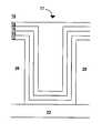
- FIG. 1is not to scale so as to more clearly show the details, and which depicts a partial cross-sectional view of a via filled with a metallization interconnection system according to the present invention
- a metallization interconnection system 10constructed according to a preferred embodiment of the present invention.
- the metallization interconnection system 10is deposited within a via 11 that is defined between sidewalls 20 , such as would be formed in a dielectric layer.
- the metallization interconnection system 10makes ohmic contact between a lower conduction layer 22 and an upper conduction layer that is not depicted.
- the first layer in the metallization system 10is a first liner layer of titanium 12 .
- the first liner layer of titanium 12functions as a gettering layer to clean out impurities that may be present in the via 11 .
- the first liner layer of titanium 12is preferably deposited using an ion metal plasma deposition method.
- ion metal plasma depositionatoms of the metal to be deposited are sputtered from a target and ionized in a plasma with a density of between about 10 10 ions/cm 3 and about 10 13 ions/cm 3 , and most preferably about 10 12 ions/cm 3 .
- the metal ionsare then drawn in a highly directional manner toward the substrate by an electrical bias on the substrate, and are uniformly deposited across the surfaces of the substrate, as mentioned above.
- Ion metal plasma depositionsuch as described herein, can be performed in a deposition chamber such as the Vectra chamber that is integrated on the Endura cluster tool platform, as manufactured by Applied Materials, Inc. of Santa Clara, Calif.
- Ion metal plasma depositionis a physical vapor deposition technique that produces a film that is visually distinguishable from those deposited by other physical vapor deposition techniques, in that it produces a film that has better coverage at the bottom of the via and less top side wall coverage.
- films deposited using ion metal plasma depositionhave good step coverage in comparison to films produced by other physical vapor deposition techniques.
- other forms of physical vapor depositionsuch as sputtering, tend to produce films that cusp at the top edges of the via 11 . This cusping of the deposited film tends to get increasingly worse as additional films are deposited, and often results in an inability to completely fill the via 11 . This situation creates several problems with the integrated circuit, and is preferably avoided.
- the first liner layer of titanium 12 as depicted in the FIGUREhas very good step coverage.
- the cross-sectional profile of the ion metal plasma deposited first liner layer of titanium 12is immediately distinguishable from other physical vapor deposition techniques, which produced a cusped film.
- the substrate on which the via 11 is disposedis brought into an ion metal plasma deposition chamber containing a titanium target, and the ion metal plasma deposition chamber is evacuated to a first base pressure.
- the first base pressureis preferably between about 10 ⁇ 9 Torr and about 10 ⁇ 6 Torr, and most preferably about 5 ⁇ 10 ⁇ 9 Torr.
- a first flow of argonis then introduced to the ion metal plasma deposition chamber.
- the first flow of argonis preferably between about 0.5 sccm and about 200 sccm, and most preferably about 20 sccm.
- the valving leading to the vacuum pumps on the ion metal plasma deposition chamberis adjusted to produce a first pressure inside of the ion metal plasma deposition chamber of between about 10 ⁇ 4 Torr and about 0.1 Torr, and most preferably about 30 ⁇ 10 ⁇ 3 Torr.
- the substrateis biased to a first voltage of between about 0 volts and about ⁇ 500 volts, and most preferably about ⁇ 150 volts, and a plasma is ignited within the ion metal plasma deposition chamber at a first power of between about 1 kilowatts and about 50 kilowatts, and most preferably about 5 kilowatts.
- a direct current power supplyis used to provide the power to ignite the plasma in the preferred embodiment.
- a radio frequency power supplymay be used.
- the substrateis held at a first temperature of between about ⁇ 50 centigrade and about 400 centigrade, and most preferably about 200 centigrade, during the ion metal plasma deposition of the first liner layer of titanium 12 .
- the deposition of the first liner layer of titanium 12proceeds for a first length of time, which is preferably a period of time of between about 1 seconds and about 100 seconds, and most preferably about 20 seconds.
- Ion metal plasma deposition for this length of time under the conditions specified aboveproduces a first liner layer of titanium 12 with a thickness of between about 5 angstroms and about 1,000 angstroms, and most preferably about 150 angstroms.
- a second liner layer of Ti x N yis deposited.
- the first liner layer of titanium 12is exposed to oxygen, such as by bringing the substrate out of the ion metal plasma deposition chamber and into the atmosphere, then the first liner layer of titanium 12 oxidizes at the surface and forms a layer of titanium oxide.
- the layer of titanium oxideincreases the resistance within the metallization interconnection layer 10 , and creates problems with the integrated circuit of which it is a part.
- thisis accomplished by depositing a second liner layer of Ti x N y 14 on top of the first liner layer of titanium 12 .
- the second liner layer of Ti x N y 14is preferably deposited in the same ion metal plasma deposition chamber as that which is used to deposit the first liner layer of titanium 12 . In this manner, there is no opportunity for the first liner layer of titanium 12 to be exposed to oxygen and form a titanium oxide layer.
- the second liner layer of Ti x N y 14is deposited within a separate ion metal plasma deposition chamber within the same cluster tool in which the ion metal plasma deposition chamber for the first liner layer of titanium 12 resides. In this manner, the substrate is again not exposed to the atmosphere between depositions of the first liner layer of titanium 12 and the second liner layer of Ti x N y 14 .
- the second liner layer of Ti x N y 14is deposited using only ion metal plasma deposition, and not any other form of physical vapor deposition or any form of chemical vapor deposition.
- Some of the purposes for this selection of deposition techniqueare to reduce the degree of cusping that is inherent with other forms of physical vapor deposition, as described elsewhere in this discussion, and further to reduce the oxidation of the first liner layer of titanium 14 that are attendant with exposing the first liner layer of titanium 14 to the atmosphere, and may be attendant with various forms of chemical vapor deposition, even if the first liner layer of titanium 14 is not exposed to the atmosphere prior to such deposition.
- a first flow of nitrogenis introduced to the ion metal plasma deposition chamber.
- the first flow of nitrogenis preferably between about 1 sccm and about 200 sccm, and most preferably about 100 sccm.
- the first flow of argonis preferably adjust to a second flow of argon at a flow rate of between about 0.5 sccm and about 100 sccm, and most preferably about 20 sccm.
- the flow rate of the first flow of argonis gradually changed to the flow rate of the second flow of argon, rather than halting the first flow of argon and then commencing the second flow of argon.
- the valving leading to the vacuum pumps on the ion metal plasma deposition chamberis adjusted to produce a second pressure inside of the ion metal plasma deposition chamber of between about 104 Torr and about 0.1 Torr, and most preferably about 30 ⁇ 10 ⁇ 3 Torr.
- the substrateis biased to a second voltage of between about 0 volts and about 400 volts, and most preferably about ⁇ 150 volts.
- the first voltageis gradually changed to the second voltage, rather than halting the first voltage and then applying the second voltage.
- a plasmais ignited within the ion metal plasma deposition chamber at a second power of between about 1 kilowatts and about 50 kilowatts, and most preferably about 2 kilowatts.
- the first power applied to the plasmais gradually adjusted to the second power applied to the plasma; rather than shutting off the first power and then re-igniting the plasma with the application of the second power.
- a direct current power supplyis used to power the plasma in the preferred embodiment.
- a radio frequency power supplymay be used.
- the substrateis held at a second temperature of between about ⁇ 50 centigrade and about 400 centigrade, and most preferably about 200 centrigrade, during the ion metal plasma deposition of the second liner layer of Ti x N y 14 .
- the deposition of the second liner layer of Ti x N y 14proceeds for a second length of time, which is preferably a period of time of between about 0.1 seconds and about 100 seconds, and most preferably about 5 seconds.
- Ion metal plasma deposition for this length of timeunder the conditions specified above produces a second liner layer of Ti x N y 14 with a thickness of between about 1 angstroms and about 300 angstroms, and most preferably about 20 angstroms.
- the plasmais preferably extinguished, and the substrate is removed from the ion metal plasma deposition chamber.
- the second liner layer of Ti x N y 14can be formed in the same chamber in which the first liner layer of titanium 12 is formed.
- the second liner layer of Ti x N y 14acts as a capping layer to the first liner layer of titanium 12 , because the second liner layer of Ti x N y 14 does not oxidize as readily when exposed to oxygen. Therefore, the substrate may be safely removed from the ion metal plasma deposition chamber at this point without fear of oxidizing the first liner layer of titanium 12 and creating the problems as described above.
- the second liner layer of Ti x N y 14is deposited using the ion metal plasma deposition process as described above, it is visually distinguishable from Ti x N y layers that are deposited with other physical vapor deposition techniques, such as sputtering. This is because the other physical vapor deposition techniques tend to produce cusping of the deposited layer at the top of the via 11 , as described above, whereas the ion metal plasma deposition produces a layer that has good step coverage.
- the second liner layer of Ti x N y 14as deposited using ion metal plasma deposition, is also visually distinguishable from layers that are deposited using chemical vapor deposition.
- a layer deposited with ion metal plasma depositionis physically distinguishable from a layer that is deposited using another deposition method.
- the metallization interconnection system 10 as described aboveis further physically distinguishable from other metallization systems in that there is no titanium oxide layer on top of the first liner layer of titanium 12 .
- the second liner layer of Ti x N y 14is purposely recited herein without a specific stoichiometry, because the processing conditions described above do not necessarily produce a film that has a single, set stoichiometry.
- the purpose of the second liner layer of Ti x N y 14is not to have a specific stoichiometry, but rather to provide a capping layer to the first liner layer of titanium 12 , so that it does not oxidize, and to do so in a manner that will not produce cusping and the problems attendant with cusping. This can be accomplished with a wide range of stoichiometries of the second liner layer of Ti x N y 14 .
- the value for Xis between about 0.45 and about 0.8, and most preferably about 0.5
- the value for Yis between about 0.55 and about 0.2, and most preferably about 0.5.
- a third liner layer of titanium nitride (TiN) 16is deposited with a stoichiometry that is more definitely set as compared to the second liner layer of Ti x N y 14 , and which is deposited such as by using a chemical vapor deposition method.
- the stoichiometry of the third liner layer of titanium nitride 16is preferably more definitely set because the third liner layer of titanium nitride 16 is intended to function as a barrier layer during later processing, and thus the third liner layer of titanium nitride 16 requires certain physical properties, such as chemical resistance, that are attendant with its set stoichiometry.
- the via 11is filled with a tungsten plug 18 , such as may be formed with a chemical vapor deposition.
- the metallization interconnection system 10is then preferably planarized and the processing of the substrate continues.
Landscapes
- Chemical & Material Sciences (AREA)
- Engineering & Computer Science (AREA)
- Metallurgy (AREA)
- Chemical Kinetics & Catalysis (AREA)
- Organic Chemistry (AREA)
- Mechanical Engineering (AREA)
- Materials Engineering (AREA)
- Microelectronics & Electronic Packaging (AREA)
- Condensed Matter Physics & Semiconductors (AREA)
- Power Engineering (AREA)
- General Physics & Mathematics (AREA)
- Computer Hardware Design (AREA)
- Physics & Mathematics (AREA)
- Manufacturing & Machinery (AREA)
- Internal Circuitry In Semiconductor Integrated Circuit Devices (AREA)
- Electrodes Of Semiconductors (AREA)
Abstract
Description
Claims (17)
Priority Applications (2)
| Application Number | Priority Date | Filing Date | Title |
|---|---|---|---|
| US09/617,550US6569751B1 (en) | 2000-07-17 | 2000-07-17 | Low via resistance system |
| US10/400,252US6893962B2 (en) | 2000-07-17 | 2003-03-27 | Low via resistance system |
Applications Claiming Priority (1)
| Application Number | Priority Date | Filing Date | Title |
|---|---|---|---|
| US09/617,550US6569751B1 (en) | 2000-07-17 | 2000-07-17 | Low via resistance system |
Related Child Applications (1)
| Application Number | Title | Priority Date | Filing Date |
|---|---|---|---|
| US10/400,252DivisionUS6893962B2 (en) | 2000-07-17 | 2003-03-27 | Low via resistance system |
Publications (1)
| Publication Number | Publication Date |
|---|---|
| US6569751B1true US6569751B1 (en) | 2003-05-27 |
Family
ID=24474090
Family Applications (2)
| Application Number | Title | Priority Date | Filing Date |
|---|---|---|---|
| US09/617,550Expired - LifetimeUS6569751B1 (en) | 2000-07-17 | 2000-07-17 | Low via resistance system |
| US10/400,252Expired - LifetimeUS6893962B2 (en) | 2000-07-17 | 2003-03-27 | Low via resistance system |
Family Applications After (1)
| Application Number | Title | Priority Date | Filing Date |
|---|---|---|---|
| US10/400,252Expired - LifetimeUS6893962B2 (en) | 2000-07-17 | 2003-03-27 | Low via resistance system |
Country Status (1)
| Country | Link |
|---|---|
| US (2) | US6569751B1 (en) |
Cited By (6)
| Publication number | Priority date | Publication date | Assignee | Title |
|---|---|---|---|---|
| US20040082167A1 (en)* | 2002-08-26 | 2004-04-29 | Jung-Hun Seo | Methods of forming aluminum structures in microelectronic articles and articles fabricated thereby |
| US20050026384A1 (en)* | 2003-07-29 | 2005-02-03 | Infineon Technologies Ag | Method for fabricating trench capacitor with insulation collar electrically connected to substrate through buried contact, in particular, for a semiconductor memory cell |
| US7101787B1 (en) | 2004-04-09 | 2006-09-05 | National Semiconductor Corporation | System and method for minimizing increases in via resistance by applying a nitrogen plasma after a titanium liner deposition |
| US20080136032A1 (en)* | 2002-04-29 | 2008-06-12 | Infineon Technologies Ag. | Method for filling a contact hole and integrated circuit arrangement with contact hole |
| US20110079918A1 (en)* | 2009-10-01 | 2011-04-07 | Applied Materials, Inc. | Plasma-based organic mask removal with silicon fluoride |
| US20160086805A1 (en)* | 2014-09-24 | 2016-03-24 | Qualcomm Incorporated | Metal-gate with an amorphous metal layer |
Families Citing this family (4)
| Publication number | Priority date | Publication date | Assignee | Title |
|---|---|---|---|---|
| WO2007023950A1 (en)* | 2005-08-26 | 2007-03-01 | Hitachi, Ltd. | Semiconductor device manufacturing method |
| US20080246124A1 (en)* | 2007-04-04 | 2008-10-09 | James Mathew | Plasma treatment of insulating material |
| JP2013128062A (en)* | 2011-12-19 | 2013-06-27 | Elpida Memory Inc | Semiconductor device manufacturing method |
| CN104157607B (en)* | 2014-09-01 | 2017-02-15 | 上海先进半导体制造股份有限公司 | Optimization method for back side pressure in tungsten deposition process |
Citations (20)
| Publication number | Priority date | Publication date | Assignee | Title |
|---|---|---|---|---|
| GB2298657A (en)* | 1995-03-04 | 1996-09-11 | Hyundai Electronics Ind | Forming metal interconnects with phase transformed titanium nitride layers |
| US5780356A (en)* | 1995-12-15 | 1998-07-14 | Hyundai Electronics Industires Co., Ltd. | Method for forming metal wire of semiconductor device |
| US6054382A (en)* | 1996-03-28 | 2000-04-25 | Texas Instruments Incorporated | Method of improving texture of metal films in semiconductor integrated circuits |
| US6080285A (en)* | 1998-09-14 | 2000-06-27 | Applied Materials, Inc. | Multiple step ionized metal plasma deposition process for conformal step coverage |
| US6100182A (en)* | 1997-06-23 | 2000-08-08 | Hyundai Electronics Industries, Co., Ltd. | Method for forming metal interconnection of semiconductor device |
| US6103618A (en)* | 1998-07-07 | 2000-08-15 | Oki Electric Industry Co., Ltd. | Method for forming an interconnection in a semiconductor element |
| US6140223A (en)* | 1997-11-25 | 2000-10-31 | Samsung Electronics Co., Ltd. | Methods of forming contacts for integrated circuits using chemical vapor deposition and physical vapor deposition |
| US6150720A (en)* | 1997-08-27 | 2000-11-21 | Yamaha Corporation | Semiconductor device having manufacturing wiring structure with buried plugs |
| US6156647A (en)* | 1997-10-27 | 2000-12-05 | Applied Materials, Inc. | Barrier layer structure which prevents migration of silicon into an adjacent metallic layer and the method of fabrication of the barrier layer |
| JP2001044201A (en)* | 1999-07-29 | 2001-02-16 | Hitachi Ltd | Method for manufacturing semiconductor integrated circuit device |
| US6251735B1 (en)* | 1999-10-29 | 2001-06-26 | Taiwan Semiconductor Manufacturing Co., Ltd. | Method of forming shallow trench isolation structure |
| US6271592B1 (en)* | 1998-02-24 | 2001-08-07 | Applied Materials, Inc. | Sputter deposited barrier layers |
| US6291342B2 (en)* | 1998-07-22 | 2001-09-18 | Samsung Electronics Co., Ltd. | Methods of forming titanium nitride composite layers using composite gases having increasing TiCl4 to NH3 ratios |
| US6303490B1 (en)* | 2000-02-09 | 2001-10-16 | Macronix International Co., Ltd. | Method for barrier layer in copper manufacture |
| US6319826B1 (en)* | 1999-01-22 | 2001-11-20 | United Microelectronics Corp. | Method of fabricating barrier layer |
| US6348731B1 (en)* | 1997-05-30 | 2002-02-19 | International Business Machines Corporation | Copper interconnections with enhanced electromigration resistance and reduced defect sensitivity and method of forming same |
| US6383929B1 (en)* | 2001-01-11 | 2002-05-07 | International Business Machines Corporation | Copper vias in low-k technology |
| US6391769B1 (en)* | 1998-08-19 | 2002-05-21 | Samsung Electronics Co., Ltd. | Method for forming metal interconnection in semiconductor device and interconnection structure fabricated thereby |
| US6420260B1 (en)* | 1997-03-27 | 2002-07-16 | Applied Materials, Inc. | Ti/Tinx underlayer which enables a highly <111> oriented aluminum interconnect |
| US6432819B1 (en)* | 1999-09-27 | 2002-08-13 | Applied Materials, Inc. | Method and apparatus of forming a sputtered doped seed layer |
Family Cites Families (3)
| Publication number | Priority date | Publication date | Assignee | Title |
|---|---|---|---|---|
| US5925225A (en)* | 1997-03-27 | 1999-07-20 | Applied Materials, Inc. | Method of producing smooth titanium nitride films having low resistivity |
| US6383915B1 (en)* | 1999-02-03 | 2002-05-07 | Applied Materials, Inc. | Tailoring of a wetting/barrier layer to reduce electromigration in an aluminum interconnect |
| US6403465B1 (en)* | 1999-12-28 | 2002-06-11 | Taiwan Semiconductor Manufacturing Company | Method to improve copper barrier properties |
- 2000
- 2000-07-17USUS09/617,550patent/US6569751B1/ennot_activeExpired - Lifetime
- 2003
- 2003-03-27USUS10/400,252patent/US6893962B2/ennot_activeExpired - Lifetime
Patent Citations (20)
| Publication number | Priority date | Publication date | Assignee | Title |
|---|---|---|---|---|
| GB2298657A (en)* | 1995-03-04 | 1996-09-11 | Hyundai Electronics Ind | Forming metal interconnects with phase transformed titanium nitride layers |
| US5780356A (en)* | 1995-12-15 | 1998-07-14 | Hyundai Electronics Industires Co., Ltd. | Method for forming metal wire of semiconductor device |
| US6054382A (en)* | 1996-03-28 | 2000-04-25 | Texas Instruments Incorporated | Method of improving texture of metal films in semiconductor integrated circuits |
| US6420260B1 (en)* | 1997-03-27 | 2002-07-16 | Applied Materials, Inc. | Ti/Tinx underlayer which enables a highly <111> oriented aluminum interconnect |
| US6348731B1 (en)* | 1997-05-30 | 2002-02-19 | International Business Machines Corporation | Copper interconnections with enhanced electromigration resistance and reduced defect sensitivity and method of forming same |
| US6100182A (en)* | 1997-06-23 | 2000-08-08 | Hyundai Electronics Industries, Co., Ltd. | Method for forming metal interconnection of semiconductor device |
| US6150720A (en)* | 1997-08-27 | 2000-11-21 | Yamaha Corporation | Semiconductor device having manufacturing wiring structure with buried plugs |
| US6156647A (en)* | 1997-10-27 | 2000-12-05 | Applied Materials, Inc. | Barrier layer structure which prevents migration of silicon into an adjacent metallic layer and the method of fabrication of the barrier layer |
| US6140223A (en)* | 1997-11-25 | 2000-10-31 | Samsung Electronics Co., Ltd. | Methods of forming contacts for integrated circuits using chemical vapor deposition and physical vapor deposition |
| US6271592B1 (en)* | 1998-02-24 | 2001-08-07 | Applied Materials, Inc. | Sputter deposited barrier layers |
| US6103618A (en)* | 1998-07-07 | 2000-08-15 | Oki Electric Industry Co., Ltd. | Method for forming an interconnection in a semiconductor element |
| US6291342B2 (en)* | 1998-07-22 | 2001-09-18 | Samsung Electronics Co., Ltd. | Methods of forming titanium nitride composite layers using composite gases having increasing TiCl4 to NH3 ratios |
| US6391769B1 (en)* | 1998-08-19 | 2002-05-21 | Samsung Electronics Co., Ltd. | Method for forming metal interconnection in semiconductor device and interconnection structure fabricated thereby |
| US6080285A (en)* | 1998-09-14 | 2000-06-27 | Applied Materials, Inc. | Multiple step ionized metal plasma deposition process for conformal step coverage |
| US6319826B1 (en)* | 1999-01-22 | 2001-11-20 | United Microelectronics Corp. | Method of fabricating barrier layer |
| JP2001044201A (en)* | 1999-07-29 | 2001-02-16 | Hitachi Ltd | Method for manufacturing semiconductor integrated circuit device |
| US6432819B1 (en)* | 1999-09-27 | 2002-08-13 | Applied Materials, Inc. | Method and apparatus of forming a sputtered doped seed layer |
| US6251735B1 (en)* | 1999-10-29 | 2001-06-26 | Taiwan Semiconductor Manufacturing Co., Ltd. | Method of forming shallow trench isolation structure |
| US6303490B1 (en)* | 2000-02-09 | 2001-10-16 | Macronix International Co., Ltd. | Method for barrier layer in copper manufacture |
| US6383929B1 (en)* | 2001-01-11 | 2002-05-07 | International Business Machines Corporation | Copper vias in low-k technology |
Cited By (9)
| Publication number | Priority date | Publication date | Assignee | Title |
|---|---|---|---|---|
| US20080136032A1 (en)* | 2002-04-29 | 2008-06-12 | Infineon Technologies Ag. | Method for filling a contact hole and integrated circuit arrangement with contact hole |
| US7825510B2 (en)* | 2002-04-29 | 2010-11-02 | Infineon Technologies Ag | Method for filling a contact hole and integrated circuit arrangement with contact hole |
| US20040082167A1 (en)* | 2002-08-26 | 2004-04-29 | Jung-Hun Seo | Methods of forming aluminum structures in microelectronic articles and articles fabricated thereby |
| US20050026384A1 (en)* | 2003-07-29 | 2005-02-03 | Infineon Technologies Ag | Method for fabricating trench capacitor with insulation collar electrically connected to substrate through buried contact, in particular, for a semiconductor memory cell |
| US7273790B2 (en)* | 2003-07-29 | 2007-09-25 | Infineon Technologies Ag | Method for fabricating trench capacitor with insulation collar electrically connected to substrate through buried contact, in particular, for a semiconductor memory cell |
| US7101787B1 (en) | 2004-04-09 | 2006-09-05 | National Semiconductor Corporation | System and method for minimizing increases in via resistance by applying a nitrogen plasma after a titanium liner deposition |
| US7531896B1 (en) | 2004-04-09 | 2009-05-12 | National Semiconductor Corporation | Semiconductor device having a minimal via resistance created by applying a nitrogen plasma to a titanium via liner |
| US20110079918A1 (en)* | 2009-10-01 | 2011-04-07 | Applied Materials, Inc. | Plasma-based organic mask removal with silicon fluoride |
| US20160086805A1 (en)* | 2014-09-24 | 2016-03-24 | Qualcomm Incorporated | Metal-gate with an amorphous metal layer |
Also Published As
| Publication number | Publication date |
|---|---|
| US20030203622A1 (en) | 2003-10-30 |
| US6893962B2 (en) | 2005-05-17 |
Similar Documents
| Publication | Publication Date | Title |
|---|---|---|
| US5801098A (en) | Method of decreasing resistivity in an electrically conductive layer | |
| US6051114A (en) | Use of pulsed-DC wafer bias for filling vias/trenches with metal in HDP physical vapor deposition | |
| US6919275B2 (en) | Method of preventing diffusion of copper through a tantalum-comprising barrier layer | |
| US5882488A (en) | Resputtering to achieve better step coverage | |
| US6080285A (en) | Multiple step ionized metal plasma deposition process for conformal step coverage | |
| US7781327B1 (en) | Resputtering process for eliminating dielectric damage | |
| JP2002118109A (en) | Damascene wiring formation method of semiconductor device and damascene wiring structure formed thereby | |
| US8765596B1 (en) | Atomic layer profiling of diffusion barrier and metal seed layers | |
| KR100501460B1 (en) | Method of filling holes in a semiconductor structure using an adhesion layer deposited from ionized metal | |
| US6569751B1 (en) | Low via resistance system | |
| US5725740A (en) | Adhesion layer for tungsten deposition | |
| US6448657B1 (en) | Structure for reducing junction spiking through a wall surface of an overetched contact via | |
| US6455921B1 (en) | Fabricating plug and near-zero overlap interconnect line | |
| KR19990063873A (en) | Improved interface between titanium and aluminum alloys in metal stacks for integrated circuits | |
| US6559000B2 (en) | Method of manufacturing a capacitor in a semiconductor device | |
| US7199040B2 (en) | Barrier layer structure | |
| KR100458297B1 (en) | Metal wiring formation method of semiconductor device | |
| US6316355B1 (en) | Method for forming metal wire using titanium film in semiconductor device having contact holes | |
| US20040180538A1 (en) | Method for producing a copper connection | |
| WO2002018653A2 (en) | Method for depositing nitride layers |
Legal Events
| Date | Code | Title | Description |
|---|---|---|---|
| AS | Assignment | Owner name:LSI LOGIC CORPORATION, CALIFORNIA Free format text:ASSIGNMENT OF ASSIGNORS INTEREST;ASSIGNORS:TRIPATH, PRABHAKAR P.;WANG, ZHIHAI;LI, WEIDAN;REEL/FRAME:011022/0051 Effective date:20000714 | |
| STCF | Information on status: patent grant | Free format text:PATENTED CASE | |
| FPAY | Fee payment | Year of fee payment:4 | |
| SULP | Surcharge for late payment | ||
| FEPP | Fee payment procedure | Free format text:PAYOR NUMBER ASSIGNED (ORIGINAL EVENT CODE: ASPN); ENTITY STATUS OF PATENT OWNER: LARGE ENTITY | |
| FPAY | Fee payment | Year of fee payment:8 | |
| AS | Assignment | Owner name:DEUTSCHE BANK AG NEW YORK BRANCH, AS COLLATERAL AG Free format text:PATENT SECURITY AGREEMENT;ASSIGNORS:LSI CORPORATION;AGERE SYSTEMS LLC;REEL/FRAME:032856/0031 Effective date:20140506 | |
| AS | Assignment | Owner name:LSI CORPORATION, CALIFORNIA Free format text:CHANGE OF NAME;ASSIGNOR:LSI LOGIC CORPORATION;REEL/FRAME:033102/0270 Effective date:20070406 | |
| FPAY | Fee payment | Year of fee payment:12 | |
| AS | Assignment | Owner name:AVAGO TECHNOLOGIES GENERAL IP (SINGAPORE) PTE. LTD Free format text:ASSIGNMENT OF ASSIGNORS INTEREST;ASSIGNOR:LSI CORPORATION;REEL/FRAME:035390/0388 Effective date:20140814 | |
| AS | Assignment | Owner name:LSI CORPORATION, CALIFORNIA Free format text:TERMINATION AND RELEASE OF SECURITY INTEREST IN PATENT RIGHTS (RELEASES RF 032856-0031);ASSIGNOR:DEUTSCHE BANK AG NEW YORK BRANCH, AS COLLATERAL AGENT;REEL/FRAME:037684/0039 Effective date:20160201 Owner name:AGERE SYSTEMS LLC, PENNSYLVANIA Free format text:TERMINATION AND RELEASE OF SECURITY INTEREST IN PATENT RIGHTS (RELEASES RF 032856-0031);ASSIGNOR:DEUTSCHE BANK AG NEW YORK BRANCH, AS COLLATERAL AGENT;REEL/FRAME:037684/0039 Effective date:20160201 | |
| AS | Assignment | Owner name:BANK OF AMERICA, N.A., AS COLLATERAL AGENT, NORTH CAROLINA Free format text:PATENT SECURITY AGREEMENT;ASSIGNOR:AVAGO TECHNOLOGIES GENERAL IP (SINGAPORE) PTE. LTD.;REEL/FRAME:037808/0001 Effective date:20160201 Owner name:BANK OF AMERICA, N.A., AS COLLATERAL AGENT, NORTH Free format text:PATENT SECURITY AGREEMENT;ASSIGNOR:AVAGO TECHNOLOGIES GENERAL IP (SINGAPORE) PTE. LTD.;REEL/FRAME:037808/0001 Effective date:20160201 | |
| AS | Assignment | Owner name:AVAGO TECHNOLOGIES GENERAL IP (SINGAPORE) PTE. LTD., SINGAPORE Free format text:TERMINATION AND RELEASE OF SECURITY INTEREST IN PATENTS;ASSIGNOR:BANK OF AMERICA, N.A., AS COLLATERAL AGENT;REEL/FRAME:041710/0001 Effective date:20170119 Owner name:AVAGO TECHNOLOGIES GENERAL IP (SINGAPORE) PTE. LTD Free format text:TERMINATION AND RELEASE OF SECURITY INTEREST IN PATENTS;ASSIGNOR:BANK OF AMERICA, N.A., AS COLLATERAL AGENT;REEL/FRAME:041710/0001 Effective date:20170119 | |
| AS | Assignment | Owner name:BELL SEMICONDUCTOR, LLC, ILLINOIS Free format text:ASSIGNMENT OF ASSIGNORS INTEREST;ASSIGNORS:AVAGO TECHNOLOGIES GENERAL IP (SINGAPORE) PTE. LTD.;BROADCOM CORPORATION;REEL/FRAME:044886/0001 Effective date:20171208 Owner name:BELL SEMICONDUCTOR, LLC, ILLINOIS Free format text:ASSIGNMENT OF ASSIGNORS INTEREST;ASSIGNORS:AVAGO TECHNOLOGIES GENERAL IP (SINGAPORE) PTE. LTD.;BROADCOM CORPORATION;REEL/FRAME:044886/0608 Effective date:20171208 | |
| AS | Assignment | Owner name:CORTLAND CAPITAL MARKET SERVICES LLC, AS COLLATERA Free format text:SECURITY INTEREST;ASSIGNORS:HILCO PATENT ACQUISITION 56, LLC;BELL SEMICONDUCTOR, LLC;BELL NORTHERN RESEARCH, LLC;REEL/FRAME:045216/0020 Effective date:20180124 | |
| AS | Assignment | Owner name:BELL NORTHERN RESEARCH, LLC, ILLINOIS Free format text:SECURITY INTEREST;ASSIGNOR:CORTLAND CAPITAL MARKET SERVICES LLC;REEL/FRAME:060885/0001 Effective date:20220401 Owner name:BELL SEMICONDUCTOR, LLC, ILLINOIS Free format text:SECURITY INTEREST;ASSIGNOR:CORTLAND CAPITAL MARKET SERVICES LLC;REEL/FRAME:060885/0001 Effective date:20220401 Owner name:HILCO PATENT ACQUISITION 56, LLC, ILLINOIS Free format text:SECURITY INTEREST;ASSIGNOR:CORTLAND CAPITAL MARKET SERVICES LLC;REEL/FRAME:060885/0001 Effective date:20220401 Owner name:BELL NORTHERN RESEARCH, LLC, ILLINOIS Free format text:RELEASE BY SECURED PARTY;ASSIGNOR:CORTLAND CAPITAL MARKET SERVICES LLC;REEL/FRAME:059720/0719 Effective date:20220401 Owner name:BELL SEMICONDUCTOR, LLC, ILLINOIS Free format text:RELEASE BY SECURED PARTY;ASSIGNOR:CORTLAND CAPITAL MARKET SERVICES LLC;REEL/FRAME:059720/0719 Effective date:20220401 Owner name:HILCO PATENT ACQUISITION 56, LLC, ILLINOIS Free format text:RELEASE BY SECURED PARTY;ASSIGNOR:CORTLAND CAPITAL MARKET SERVICES LLC;REEL/FRAME:059720/0719 Effective date:20220401 |