US6569382B1 - Methods apparatus for the electronic, homogeneous assembly and fabrication of devices - Google Patents
Methods apparatus for the electronic, homogeneous assembly and fabrication of devicesDownload PDFInfo
- Publication number
- US6569382B1 US6569382B1US09/436,311US43631199AUS6569382B1US 6569382 B1US6569382 B1US 6569382B1US 43631199 AUS43631199 AUS 43631199AUS 6569382 B1US6569382 B1US 6569382B1
- Authority
- US
- United States
- Prior art keywords
- devices
- dna
- assembly
- component device
- self
- Prior art date
- Legal status (The legal status is an assumption and is not a legal conclusion. Google has not performed a legal analysis and makes no representation as to the accuracy of the status listed.)
- Expired - Fee Related
Links
Images


Classifications
- C—CHEMISTRY; METALLURGY
- C12—BIOCHEMISTRY; BEER; SPIRITS; WINE; VINEGAR; MICROBIOLOGY; ENZYMOLOGY; MUTATION OR GENETIC ENGINEERING
- C12Q—MEASURING OR TESTING PROCESSES INVOLVING ENZYMES, NUCLEIC ACIDS OR MICROORGANISMS; COMPOSITIONS OR TEST PAPERS THEREFOR; PROCESSES OF PREPARING SUCH COMPOSITIONS; CONDITION-RESPONSIVE CONTROL IN MICROBIOLOGICAL OR ENZYMOLOGICAL PROCESSES
- C12Q1/00—Measuring or testing processes involving enzymes, nucleic acids or microorganisms; Compositions therefor; Processes of preparing such compositions
- H—ELECTRICITY
- H01—ELECTRIC ELEMENTS
- H01L—SEMICONDUCTOR DEVICES NOT COVERED BY CLASS H10
- H01L24/00—Arrangements for connecting or disconnecting semiconductor or solid-state bodies; Methods or apparatus related thereto
- H01L24/93—Batch processes
- H01L24/95—Batch processes at chip-level, i.e. with connecting carried out on a plurality of singulated devices, i.e. on diced chips
- B—PERFORMING OPERATIONS; TRANSPORTING
- B01—PHYSICAL OR CHEMICAL PROCESSES OR APPARATUS IN GENERAL
- B01J—CHEMICAL OR PHYSICAL PROCESSES, e.g. CATALYSIS OR COLLOID CHEMISTRY; THEIR RELEVANT APPARATUS
- B01J19/00—Chemical, physical or physico-chemical processes in general; Their relevant apparatus
- B01J19/0046—Sequential or parallel reactions, e.g. for the synthesis of polypeptides or polynucleotides; Apparatus and devices for combinatorial chemistry or for making molecular arrays
- B—PERFORMING OPERATIONS; TRANSPORTING
- B01—PHYSICAL OR CHEMICAL PROCESSES OR APPARATUS IN GENERAL
- B01J—CHEMICAL OR PHYSICAL PROCESSES, e.g. CATALYSIS OR COLLOID CHEMISTRY; THEIR RELEVANT APPARATUS
- B01J19/00—Chemical, physical or physico-chemical processes in general; Their relevant apparatus
- B01J19/0093—Microreactors, e.g. miniaturised or microfabricated reactors
- B—PERFORMING OPERATIONS; TRANSPORTING
- B01—PHYSICAL OR CHEMICAL PROCESSES OR APPARATUS IN GENERAL
- B01L—CHEMICAL OR PHYSICAL LABORATORY APPARATUS FOR GENERAL USE
- B01L3/00—Containers or dishes for laboratory use, e.g. laboratory glassware; Droppers
- B01L3/50—Containers for the purpose of retaining a material to be analysed, e.g. test tubes
- B01L3/502—Containers for the purpose of retaining a material to be analysed, e.g. test tubes with fluid transport, e.g. in multi-compartment structures
- B01L3/5027—Containers for the purpose of retaining a material to be analysed, e.g. test tubes with fluid transport, e.g. in multi-compartment structures by integrated microfluidic structures, i.e. dimensions of channels and chambers are such that surface tension forces are important, e.g. lab-on-a-chip
- B01L3/502707—Containers for the purpose of retaining a material to be analysed, e.g. test tubes with fluid transport, e.g. in multi-compartment structures by integrated microfluidic structures, i.e. dimensions of channels and chambers are such that surface tension forces are important, e.g. lab-on-a-chip characterised by the manufacture of the container or its components
- B—PERFORMING OPERATIONS; TRANSPORTING
- B01—PHYSICAL OR CHEMICAL PROCESSES OR APPARATUS IN GENERAL
- B01L—CHEMICAL OR PHYSICAL LABORATORY APPARATUS FOR GENERAL USE
- B01L3/00—Containers or dishes for laboratory use, e.g. laboratory glassware; Droppers
- B01L3/50—Containers for the purpose of retaining a material to be analysed, e.g. test tubes
- B01L3/502—Containers for the purpose of retaining a material to be analysed, e.g. test tubes with fluid transport, e.g. in multi-compartment structures
- B01L3/5027—Containers for the purpose of retaining a material to be analysed, e.g. test tubes with fluid transport, e.g. in multi-compartment structures by integrated microfluidic structures, i.e. dimensions of channels and chambers are such that surface tension forces are important, e.g. lab-on-a-chip
- B01L3/502715—Containers for the purpose of retaining a material to be analysed, e.g. test tubes with fluid transport, e.g. in multi-compartment structures by integrated microfluidic structures, i.e. dimensions of channels and chambers are such that surface tension forces are important, e.g. lab-on-a-chip characterised by interfacing components, e.g. fluidic, electrical, optical or mechanical interfaces
- B—PERFORMING OPERATIONS; TRANSPORTING
- B01—PHYSICAL OR CHEMICAL PROCESSES OR APPARATUS IN GENERAL
- B01L—CHEMICAL OR PHYSICAL LABORATORY APPARATUS FOR GENERAL USE
- B01L3/00—Containers or dishes for laboratory use, e.g. laboratory glassware; Droppers
- B01L3/50—Containers for the purpose of retaining a material to be analysed, e.g. test tubes
- B01L3/502—Containers for the purpose of retaining a material to be analysed, e.g. test tubes with fluid transport, e.g. in multi-compartment structures
- B01L3/5027—Containers for the purpose of retaining a material to be analysed, e.g. test tubes with fluid transport, e.g. in multi-compartment structures by integrated microfluidic structures, i.e. dimensions of channels and chambers are such that surface tension forces are important, e.g. lab-on-a-chip
- B01L3/502761—Containers for the purpose of retaining a material to be analysed, e.g. test tubes with fluid transport, e.g. in multi-compartment structures by integrated microfluidic structures, i.e. dimensions of channels and chambers are such that surface tension forces are important, e.g. lab-on-a-chip specially adapted for handling suspended solids or molecules independently from the bulk fluid flow, e.g. for trapping or sorting beads, for physically stretching molecules
- B—PERFORMING OPERATIONS; TRANSPORTING
- B01—PHYSICAL OR CHEMICAL PROCESSES OR APPARATUS IN GENERAL
- B01L—CHEMICAL OR PHYSICAL LABORATORY APPARATUS FOR GENERAL USE
- B01L9/00—Supporting devices; Holding devices
- B01L9/52—Supports specially adapted for flat sample carriers, e.g. for plates, slides, chips
- B—PERFORMING OPERATIONS; TRANSPORTING
- B82—NANOTECHNOLOGY
- B82B—NANOSTRUCTURES FORMED BY MANIPULATION OF INDIVIDUAL ATOMS, MOLECULES, OR LIMITED COLLECTIONS OF ATOMS OR MOLECULES AS DISCRETE UNITS; MANUFACTURE OR TREATMENT THEREOF
- B82B3/00—Manufacture or treatment of nanostructures by manipulation of individual atoms or molecules, or limited collections of atoms or molecules as discrete units
- B—PERFORMING OPERATIONS; TRANSPORTING
- B82—NANOTECHNOLOGY
- B82Y—SPECIFIC USES OR APPLICATIONS OF NANOSTRUCTURES; MEASUREMENT OR ANALYSIS OF NANOSTRUCTURES; MANUFACTURE OR TREATMENT OF NANOSTRUCTURES
- B82Y10/00—Nanotechnology for information processing, storage or transmission, e.g. quantum computing or single electron logic
- B—PERFORMING OPERATIONS; TRANSPORTING
- B82—NANOTECHNOLOGY
- B82Y—SPECIFIC USES OR APPLICATIONS OF NANOSTRUCTURES; MEASUREMENT OR ANALYSIS OF NANOSTRUCTURES; MANUFACTURE OR TREATMENT OF NANOSTRUCTURES
- B82Y20/00—Nanooptics, e.g. quantum optics or photonic crystals
- B—PERFORMING OPERATIONS; TRANSPORTING
- B82—NANOTECHNOLOGY
- B82Y—SPECIFIC USES OR APPLICATIONS OF NANOSTRUCTURES; MEASUREMENT OR ANALYSIS OF NANOSTRUCTURES; MANUFACTURE OR TREATMENT OF NANOSTRUCTURES
- B82Y30/00—Nanotechnology for materials or surface science, e.g. nanocomposites
- B—PERFORMING OPERATIONS; TRANSPORTING
- B82—NANOTECHNOLOGY
- B82Y—SPECIFIC USES OR APPLICATIONS OF NANOSTRUCTURES; MEASUREMENT OR ANALYSIS OF NANOSTRUCTURES; MANUFACTURE OR TREATMENT OF NANOSTRUCTURES
- B82Y40/00—Manufacture or treatment of nanostructures
- C—CHEMISTRY; METALLURGY
- C07—ORGANIC CHEMISTRY
- C07H—SUGARS; DERIVATIVES THEREOF; NUCLEOSIDES; NUCLEOTIDES; NUCLEIC ACIDS
- C07H21/00—Compounds containing two or more mononucleotide units having separate phosphate or polyphosphate groups linked by saccharide radicals of nucleoside groups, e.g. nucleic acids
- C—CHEMISTRY; METALLURGY
- C07—ORGANIC CHEMISTRY
- C07K—PEPTIDES
- C07K1/00—General methods for the preparation of peptides, i.e. processes for the organic chemical preparation of peptides or proteins of any length
- C07K1/04—General methods for the preparation of peptides, i.e. processes for the organic chemical preparation of peptides or proteins of any length on carriers
- C07K1/045—General methods for the preparation of peptides, i.e. processes for the organic chemical preparation of peptides or proteins of any length on carriers using devices to improve synthesis, e.g. reactors, special vessels
- C—CHEMISTRY; METALLURGY
- C07—ORGANIC CHEMISTRY
- C07K—PEPTIDES
- C07K1/00—General methods for the preparation of peptides, i.e. processes for the organic chemical preparation of peptides or proteins of any length
- C07K1/04—General methods for the preparation of peptides, i.e. processes for the organic chemical preparation of peptides or proteins of any length on carriers
- C07K1/047—Simultaneous synthesis of different peptide species; Peptide libraries
- G—PHYSICS
- G01—MEASURING; TESTING
- G01N—INVESTIGATING OR ANALYSING MATERIALS BY DETERMINING THEIR CHEMICAL OR PHYSICAL PROPERTIES
- G01N33/00—Investigating or analysing materials by specific methods not covered by groups G01N1/00 - G01N31/00
- G01N33/48—Biological material, e.g. blood, urine; Haemocytometers
- G01N33/50—Chemical analysis of biological material, e.g. blood, urine; Testing involving biospecific ligand binding methods; Immunological testing
- G01N33/53—Immunoassay; Biospecific binding assay; Materials therefor
- G01N33/543—Immunoassay; Biospecific binding assay; Materials therefor with an insoluble carrier for immobilising immunochemicals
- G01N33/54366—Apparatus specially adapted for solid-phase testing
- G—PHYSICS
- G02—OPTICS
- G02B—OPTICAL ELEMENTS, SYSTEMS OR APPARATUS
- G02B6/00—Light guides; Structural details of arrangements comprising light guides and other optical elements, e.g. couplings
- G02B6/10—Light guides; Structural details of arrangements comprising light guides and other optical elements, e.g. couplings of the optical waveguide type
- G02B6/12—Light guides; Structural details of arrangements comprising light guides and other optical elements, e.g. couplings of the optical waveguide type of the integrated circuit kind
- G02B6/122—Basic optical elements, e.g. light-guiding paths
- G02B6/1225—Basic optical elements, e.g. light-guiding paths comprising photonic band-gap structures or photonic lattices
- G—PHYSICS
- G06—COMPUTING OR CALCULATING; COUNTING
- G06N—COMPUTING ARRANGEMENTS BASED ON SPECIFIC COMPUTATIONAL MODELS
- G06N3/00—Computing arrangements based on biological models
- G06N3/002—Biomolecular computers, i.e. using biomolecules, proteins, cells
- G—PHYSICS
- G06—COMPUTING OR CALCULATING; COUNTING
- G06N—COMPUTING ARRANGEMENTS BASED ON SPECIFIC COMPUTATIONAL MODELS
- G06N3/00—Computing arrangements based on biological models
- G06N3/02—Neural networks
- G06N3/06—Physical realisation, i.e. hardware implementation of neural networks, neurons or parts of neurons
- G06N3/061—Physical realisation, i.e. hardware implementation of neural networks, neurons or parts of neurons using biological neurons, e.g. biological neurons connected to an integrated circuit
- G—PHYSICS
- G06—COMPUTING OR CALCULATING; COUNTING
- G06N—COMPUTING ARRANGEMENTS BASED ON SPECIFIC COMPUTATIONAL MODELS
- G06N3/00—Computing arrangements based on biological models
- G06N3/12—Computing arrangements based on biological models using genetic models
- G06N3/123—DNA computing
- G—PHYSICS
- G11—INFORMATION STORAGE
- G11B—INFORMATION STORAGE BASED ON RELATIVE MOVEMENT BETWEEN RECORD CARRIER AND TRANSDUCER
- G11B7/00—Recording or reproducing by optical means, e.g. recording using a thermal beam of optical radiation by modifying optical properties or the physical structure, reproducing using an optical beam at lower power by sensing optical properties; Record carriers therefor
- G11B7/004—Recording, reproducing or erasing methods; Read, write or erase circuits therefor
- G11B7/0045—Recording
- G11B7/00455—Recording involving reflectivity, absorption or colour changes
- G—PHYSICS
- G11—INFORMATION STORAGE
- G11B—INFORMATION STORAGE BASED ON RELATIVE MOVEMENT BETWEEN RECORD CARRIER AND TRANSDUCER
- G11B7/00—Recording or reproducing by optical means, e.g. recording using a thermal beam of optical radiation by modifying optical properties or the physical structure, reproducing using an optical beam at lower power by sensing optical properties; Record carriers therefor
- G11B7/004—Recording, reproducing or erasing methods; Read, write or erase circuits therefor
- G11B7/005—Reproducing
- G11B7/0052—Reproducing involving reflectivity, absorption or colour changes
- G—PHYSICS
- G11—INFORMATION STORAGE
- G11B—INFORMATION STORAGE BASED ON RELATIVE MOVEMENT BETWEEN RECORD CARRIER AND TRANSDUCER
- G11B7/00—Recording or reproducing by optical means, e.g. recording using a thermal beam of optical radiation by modifying optical properties or the physical structure, reproducing using an optical beam at lower power by sensing optical properties; Record carriers therefor
- G11B7/24—Record carriers characterised by shape, structure or physical properties, or by the selection of the material
- G11B7/241—Record carriers characterised by shape, structure or physical properties, or by the selection of the material characterised by the selection of the material
- G11B7/242—Record carriers characterised by shape, structure or physical properties, or by the selection of the material characterised by the selection of the material of recording layers
- G11B7/244—Record carriers characterised by shape, structure or physical properties, or by the selection of the material characterised by the selection of the material of recording layers comprising organic materials only
- G—PHYSICS
- G11—INFORMATION STORAGE
- G11C—STATIC STORES
- G11C13/00—Digital stores characterised by the use of storage elements not covered by groups G11C11/00, G11C23/00, or G11C25/00
- G11C13/0002—Digital stores characterised by the use of storage elements not covered by groups G11C11/00, G11C23/00, or G11C25/00 using resistive RAM [RRAM] elements
- G11C13/0009—RRAM elements whose operation depends upon chemical change
- G11C13/0014—RRAM elements whose operation depends upon chemical change comprising cells based on organic memory material
- G11C13/0019—RRAM elements whose operation depends upon chemical change comprising cells based on organic memory material comprising bio-molecules
- G—PHYSICS
- G11—INFORMATION STORAGE
- G11C—STATIC STORES
- G11C19/00—Digital stores in which the information is moved stepwise, e.g. shift registers
- H—ELECTRICITY
- H01—ELECTRIC ELEMENTS
- H01L—SEMICONDUCTOR DEVICES NOT COVERED BY CLASS H10
- H01L25/00—Assemblies consisting of a plurality of semiconductor or other solid state devices
- H01L25/50—Multistep manufacturing processes of assemblies consisting of devices, the devices being individual devices of subclass H10D or integrated devices of class H10
- H—ELECTRICITY
- H10—SEMICONDUCTOR DEVICES; ELECTRIC SOLID-STATE DEVICES NOT OTHERWISE PROVIDED FOR
- H10D—INORGANIC ELECTRIC SEMICONDUCTOR DEVICES
- H10D30/00—Field-effect transistors [FET]
- H10D30/01—Manufacture or treatment
- H10D30/021—Manufacture or treatment of FETs having insulated gates [IGFET]
- H10D30/0223—Manufacture or treatment of FETs having insulated gates [IGFET] having source and drain regions or source and drain extensions self-aligned to sides of the gate
- H10D30/0227—Manufacture or treatment of FETs having insulated gates [IGFET] having source and drain regions or source and drain extensions self-aligned to sides of the gate having both lightly-doped source and drain extensions and source and drain regions self-aligned to the sides of the gate, e.g. lightly-doped drain [LDD] MOSFET or double-diffused drain [DDD] MOSFET
- H—ELECTRICITY
- H10—SEMICONDUCTOR DEVICES; ELECTRIC SOLID-STATE DEVICES NOT OTHERWISE PROVIDED FOR
- H10D—INORGANIC ELECTRIC SEMICONDUCTOR DEVICES
- H10D30/00—Field-effect transistors [FET]
- H10D30/01—Manufacture or treatment
- H10D30/021—Manufacture or treatment of FETs having insulated gates [IGFET]
- H10D30/027—Manufacture or treatment of FETs having insulated gates [IGFET] of lateral single-gate IGFETs
- H10D30/0275—Manufacture or treatment of FETs having insulated gates [IGFET] of lateral single-gate IGFETs forming single crystalline semiconductor source or drain regions resulting in recessed gates, e.g. forming raised source or drain regions
- H—ELECTRICITY
- H10—SEMICONDUCTOR DEVICES; ELECTRIC SOLID-STATE DEVICES NOT OTHERWISE PROVIDED FOR
- H10D—INORGANIC ELECTRIC SEMICONDUCTOR DEVICES
- H10D30/00—Field-effect transistors [FET]
- H10D30/60—Insulated-gate field-effect transistors [IGFET]
- H10D30/601—Insulated-gate field-effect transistors [IGFET] having lightly-doped drain or source extensions, e.g. LDD IGFETs or DDD IGFETs
- H10D30/608—Insulated-gate field-effect transistors [IGFET] having lightly-doped drain or source extensions, e.g. LDD IGFETs or DDD IGFETs having non-planar bodies, e.g. having recessed gate electrodes
- H—ELECTRICITY
- H10—SEMICONDUCTOR DEVICES; ELECTRIC SOLID-STATE DEVICES NOT OTHERWISE PROVIDED FOR
- H10D—INORGANIC ELECTRIC SEMICONDUCTOR DEVICES
- H10D64/00—Electrodes of devices having potential barriers
- H10D64/01—Manufacture or treatment
- H10D64/021—Manufacture or treatment using multiple gate spacer layers, e.g. bilayered sidewall spacers
- H—ELECTRICITY
- H10—SEMICONDUCTOR DEVICES; ELECTRIC SOLID-STATE DEVICES NOT OTHERWISE PROVIDED FOR
- H10K—ORGANIC ELECTRIC SOLID-STATE DEVICES
- H10K10/00—Organic devices specially adapted for rectifying, amplifying, oscillating or switching; Organic capacitors or resistors having potential barriers
- H10K10/701—Organic molecular electronic devices
- B—PERFORMING OPERATIONS; TRANSPORTING
- B01—PHYSICAL OR CHEMICAL PROCESSES OR APPARATUS IN GENERAL
- B01J—CHEMICAL OR PHYSICAL PROCESSES, e.g. CATALYSIS OR COLLOID CHEMISTRY; THEIR RELEVANT APPARATUS
- B01J2219/00—Chemical, physical or physico-chemical processes in general; Their relevant apparatus
- B01J2219/00274—Sequential or parallel reactions; Apparatus and devices for combinatorial chemistry or for making arrays; Chemical library technology
- B01J2219/00277—Apparatus
- B01J2219/00279—Features relating to reactor vessels
- B01J2219/00306—Reactor vessels in a multiple arrangement
- B01J2219/00313—Reactor vessels in a multiple arrangement the reactor vessels being formed by arrays of wells in blocks
- B01J2219/00315—Microtiter plates
- B01J2219/00317—Microwell devices, i.e. having large numbers of wells
- B—PERFORMING OPERATIONS; TRANSPORTING
- B01—PHYSICAL OR CHEMICAL PROCESSES OR APPARATUS IN GENERAL
- B01J—CHEMICAL OR PHYSICAL PROCESSES, e.g. CATALYSIS OR COLLOID CHEMISTRY; THEIR RELEVANT APPARATUS
- B01J2219/00—Chemical, physical or physico-chemical processes in general; Their relevant apparatus
- B01J2219/00274—Sequential or parallel reactions; Apparatus and devices for combinatorial chemistry or for making arrays; Chemical library technology
- B01J2219/00277—Apparatus
- B01J2219/00351—Means for dispensing and evacuation of reagents
- B01J2219/00427—Means for dispensing and evacuation of reagents using masks
- B01J2219/00432—Photolithographic masks
- B—PERFORMING OPERATIONS; TRANSPORTING
- B01—PHYSICAL OR CHEMICAL PROCESSES OR APPARATUS IN GENERAL
- B01J—CHEMICAL OR PHYSICAL PROCESSES, e.g. CATALYSIS OR COLLOID CHEMISTRY; THEIR RELEVANT APPARATUS
- B01J2219/00—Chemical, physical or physico-chemical processes in general; Their relevant apparatus
- B01J2219/00274—Sequential or parallel reactions; Apparatus and devices for combinatorial chemistry or for making arrays; Chemical library technology
- B01J2219/00277—Apparatus
- B01J2219/00497—Features relating to the solid phase supports
- B01J2219/00527—Sheets
- B01J2219/00529—DNA chips
- B—PERFORMING OPERATIONS; TRANSPORTING
- B01—PHYSICAL OR CHEMICAL PROCESSES OR APPARATUS IN GENERAL
- B01J—CHEMICAL OR PHYSICAL PROCESSES, e.g. CATALYSIS OR COLLOID CHEMISTRY; THEIR RELEVANT APPARATUS
- B01J2219/00—Chemical, physical or physico-chemical processes in general; Their relevant apparatus
- B01J2219/00274—Sequential or parallel reactions; Apparatus and devices for combinatorial chemistry or for making arrays; Chemical library technology
- B01J2219/00277—Apparatus
- B01J2219/00497—Features relating to the solid phase supports
- B01J2219/00527—Sheets
- B01J2219/00536—Sheets in the shape of disks
- B—PERFORMING OPERATIONS; TRANSPORTING
- B01—PHYSICAL OR CHEMICAL PROCESSES OR APPARATUS IN GENERAL
- B01J—CHEMICAL OR PHYSICAL PROCESSES, e.g. CATALYSIS OR COLLOID CHEMISTRY; THEIR RELEVANT APPARATUS
- B01J2219/00—Chemical, physical or physico-chemical processes in general; Their relevant apparatus
- B01J2219/00274—Sequential or parallel reactions; Apparatus and devices for combinatorial chemistry or for making arrays; Chemical library technology
- B01J2219/00277—Apparatus
- B01J2219/0054—Means for coding or tagging the apparatus or the reagents
- B01J2219/00545—Colours
- B—PERFORMING OPERATIONS; TRANSPORTING
- B01—PHYSICAL OR CHEMICAL PROCESSES OR APPARATUS IN GENERAL
- B01J—CHEMICAL OR PHYSICAL PROCESSES, e.g. CATALYSIS OR COLLOID CHEMISTRY; THEIR RELEVANT APPARATUS
- B01J2219/00—Chemical, physical or physico-chemical processes in general; Their relevant apparatus
- B01J2219/00274—Sequential or parallel reactions; Apparatus and devices for combinatorial chemistry or for making arrays; Chemical library technology
- B01J2219/00583—Features relative to the processes being carried out
- B01J2219/00585—Parallel processes
- B—PERFORMING OPERATIONS; TRANSPORTING
- B01—PHYSICAL OR CHEMICAL PROCESSES OR APPARATUS IN GENERAL
- B01J—CHEMICAL OR PHYSICAL PROCESSES, e.g. CATALYSIS OR COLLOID CHEMISTRY; THEIR RELEVANT APPARATUS
- B01J2219/00—Chemical, physical or physico-chemical processes in general; Their relevant apparatus
- B01J2219/00274—Sequential or parallel reactions; Apparatus and devices for combinatorial chemistry or for making arrays; Chemical library technology
- B01J2219/00583—Features relative to the processes being carried out
- B01J2219/0059—Sequential processes
- B—PERFORMING OPERATIONS; TRANSPORTING
- B01—PHYSICAL OR CHEMICAL PROCESSES OR APPARATUS IN GENERAL
- B01J—CHEMICAL OR PHYSICAL PROCESSES, e.g. CATALYSIS OR COLLOID CHEMISTRY; THEIR RELEVANT APPARATUS
- B01J2219/00—Chemical, physical or physico-chemical processes in general; Their relevant apparatus
- B01J2219/00274—Sequential or parallel reactions; Apparatus and devices for combinatorial chemistry or for making arrays; Chemical library technology
- B01J2219/00583—Features relative to the processes being carried out
- B01J2219/00596—Solid-phase processes
- B—PERFORMING OPERATIONS; TRANSPORTING
- B01—PHYSICAL OR CHEMICAL PROCESSES OR APPARATUS IN GENERAL
- B01J—CHEMICAL OR PHYSICAL PROCESSES, e.g. CATALYSIS OR COLLOID CHEMISTRY; THEIR RELEVANT APPARATUS
- B01J2219/00—Chemical, physical or physico-chemical processes in general; Their relevant apparatus
- B01J2219/00274—Sequential or parallel reactions; Apparatus and devices for combinatorial chemistry or for making arrays; Chemical library technology
- B01J2219/00583—Features relative to the processes being carried out
- B01J2219/00603—Making arrays on substantially continuous surfaces
- B01J2219/00605—Making arrays on substantially continuous surfaces the compounds being directly bound or immobilised to solid supports
- B01J2219/00608—DNA chips
- B—PERFORMING OPERATIONS; TRANSPORTING
- B01—PHYSICAL OR CHEMICAL PROCESSES OR APPARATUS IN GENERAL
- B01J—CHEMICAL OR PHYSICAL PROCESSES, e.g. CATALYSIS OR COLLOID CHEMISTRY; THEIR RELEVANT APPARATUS
- B01J2219/00—Chemical, physical or physico-chemical processes in general; Their relevant apparatus
- B01J2219/00274—Sequential or parallel reactions; Apparatus and devices for combinatorial chemistry or for making arrays; Chemical library technology
- B01J2219/00583—Features relative to the processes being carried out
- B01J2219/00603—Making arrays on substantially continuous surfaces
- B01J2219/00605—Making arrays on substantially continuous surfaces the compounds being directly bound or immobilised to solid supports
- B01J2219/00612—Making arrays on substantially continuous surfaces the compounds being directly bound or immobilised to solid supports the surface being inorganic
- B—PERFORMING OPERATIONS; TRANSPORTING
- B01—PHYSICAL OR CHEMICAL PROCESSES OR APPARATUS IN GENERAL
- B01J—CHEMICAL OR PHYSICAL PROCESSES, e.g. CATALYSIS OR COLLOID CHEMISTRY; THEIR RELEVANT APPARATUS
- B01J2219/00—Chemical, physical or physico-chemical processes in general; Their relevant apparatus
- B01J2219/00274—Sequential or parallel reactions; Apparatus and devices for combinatorial chemistry or for making arrays; Chemical library technology
- B01J2219/00583—Features relative to the processes being carried out
- B01J2219/00603—Making arrays on substantially continuous surfaces
- B01J2219/00605—Making arrays on substantially continuous surfaces the compounds being directly bound or immobilised to solid supports
- B01J2219/00614—Delimitation of the attachment areas
- B—PERFORMING OPERATIONS; TRANSPORTING
- B01—PHYSICAL OR CHEMICAL PROCESSES OR APPARATUS IN GENERAL
- B01J—CHEMICAL OR PHYSICAL PROCESSES, e.g. CATALYSIS OR COLLOID CHEMISTRY; THEIR RELEVANT APPARATUS
- B01J2219/00—Chemical, physical or physico-chemical processes in general; Their relevant apparatus
- B01J2219/00274—Sequential or parallel reactions; Apparatus and devices for combinatorial chemistry or for making arrays; Chemical library technology
- B01J2219/00583—Features relative to the processes being carried out
- B01J2219/00603—Making arrays on substantially continuous surfaces
- B01J2219/00605—Making arrays on substantially continuous surfaces the compounds being directly bound or immobilised to solid supports
- B01J2219/00623—Immobilisation or binding
- B01J2219/00626—Covalent
- B—PERFORMING OPERATIONS; TRANSPORTING
- B01—PHYSICAL OR CHEMICAL PROCESSES OR APPARATUS IN GENERAL
- B01J—CHEMICAL OR PHYSICAL PROCESSES, e.g. CATALYSIS OR COLLOID CHEMISTRY; THEIR RELEVANT APPARATUS
- B01J2219/00—Chemical, physical or physico-chemical processes in general; Their relevant apparatus
- B01J2219/00274—Sequential or parallel reactions; Apparatus and devices for combinatorial chemistry or for making arrays; Chemical library technology
- B01J2219/00583—Features relative to the processes being carried out
- B01J2219/00603—Making arrays on substantially continuous surfaces
- B01J2219/00605—Making arrays on substantially continuous surfaces the compounds being directly bound or immobilised to solid supports
- B01J2219/00632—Introduction of reactive groups to the surface
- B01J2219/00637—Introduction of reactive groups to the surface by coating it with another layer
- B—PERFORMING OPERATIONS; TRANSPORTING
- B01—PHYSICAL OR CHEMICAL PROCESSES OR APPARATUS IN GENERAL
- B01J—CHEMICAL OR PHYSICAL PROCESSES, e.g. CATALYSIS OR COLLOID CHEMISTRY; THEIR RELEVANT APPARATUS
- B01J2219/00—Chemical, physical or physico-chemical processes in general; Their relevant apparatus
- B01J2219/00274—Sequential or parallel reactions; Apparatus and devices for combinatorial chemistry or for making arrays; Chemical library technology
- B01J2219/00583—Features relative to the processes being carried out
- B01J2219/00603—Making arrays on substantially continuous surfaces
- B01J2219/00653—Making arrays on substantially continuous surfaces the compounds being bound to electrodes embedded in or on the solid supports
- B—PERFORMING OPERATIONS; TRANSPORTING
- B01—PHYSICAL OR CHEMICAL PROCESSES OR APPARATUS IN GENERAL
- B01J—CHEMICAL OR PHYSICAL PROCESSES, e.g. CATALYSIS OR COLLOID CHEMISTRY; THEIR RELEVANT APPARATUS
- B01J2219/00—Chemical, physical or physico-chemical processes in general; Their relevant apparatus
- B01J2219/00274—Sequential or parallel reactions; Apparatus and devices for combinatorial chemistry or for making arrays; Chemical library technology
- B01J2219/00583—Features relative to the processes being carried out
- B01J2219/00603—Making arrays on substantially continuous surfaces
- B01J2219/00659—Two-dimensional arrays
- B—PERFORMING OPERATIONS; TRANSPORTING
- B01—PHYSICAL OR CHEMICAL PROCESSES OR APPARATUS IN GENERAL
- B01J—CHEMICAL OR PHYSICAL PROCESSES, e.g. CATALYSIS OR COLLOID CHEMISTRY; THEIR RELEVANT APPARATUS
- B01J2219/00—Chemical, physical or physico-chemical processes in general; Their relevant apparatus
- B01J2219/00274—Sequential or parallel reactions; Apparatus and devices for combinatorial chemistry or for making arrays; Chemical library technology
- B01J2219/00583—Features relative to the processes being carried out
- B01J2219/00603—Making arrays on substantially continuous surfaces
- B01J2219/00677—Ex-situ synthesis followed by deposition on the substrate
- B—PERFORMING OPERATIONS; TRANSPORTING
- B01—PHYSICAL OR CHEMICAL PROCESSES OR APPARATUS IN GENERAL
- B01J—CHEMICAL OR PHYSICAL PROCESSES, e.g. CATALYSIS OR COLLOID CHEMISTRY; THEIR RELEVANT APPARATUS
- B01J2219/00—Chemical, physical or physico-chemical processes in general; Their relevant apparatus
- B01J2219/00274—Sequential or parallel reactions; Apparatus and devices for combinatorial chemistry or for making arrays; Chemical library technology
- B01J2219/0068—Means for controlling the apparatus of the process
- B01J2219/00686—Automatic
- B01J2219/00689—Automatic using computers
- B—PERFORMING OPERATIONS; TRANSPORTING
- B01—PHYSICAL OR CHEMICAL PROCESSES OR APPARATUS IN GENERAL
- B01J—CHEMICAL OR PHYSICAL PROCESSES, e.g. CATALYSIS OR COLLOID CHEMISTRY; THEIR RELEVANT APPARATUS
- B01J2219/00—Chemical, physical or physico-chemical processes in general; Their relevant apparatus
- B01J2219/00274—Sequential or parallel reactions; Apparatus and devices for combinatorial chemistry or for making arrays; Chemical library technology
- B01J2219/0068—Means for controlling the apparatus of the process
- B01J2219/00702—Processes involving means for analysing and characterising the products
- B01J2219/00707—Processes involving means for analysing and characterising the products separated from the reactor apparatus
- B—PERFORMING OPERATIONS; TRANSPORTING
- B01—PHYSICAL OR CHEMICAL PROCESSES OR APPARATUS IN GENERAL
- B01J—CHEMICAL OR PHYSICAL PROCESSES, e.g. CATALYSIS OR COLLOID CHEMISTRY; THEIR RELEVANT APPARATUS
- B01J2219/00—Chemical, physical or physico-chemical processes in general; Their relevant apparatus
- B01J2219/00274—Sequential or parallel reactions; Apparatus and devices for combinatorial chemistry or for making arrays; Chemical library technology
- B01J2219/00709—Type of synthesis
- B01J2219/00711—Light-directed synthesis
- B—PERFORMING OPERATIONS; TRANSPORTING
- B01—PHYSICAL OR CHEMICAL PROCESSES OR APPARATUS IN GENERAL
- B01J—CHEMICAL OR PHYSICAL PROCESSES, e.g. CATALYSIS OR COLLOID CHEMISTRY; THEIR RELEVANT APPARATUS
- B01J2219/00—Chemical, physical or physico-chemical processes in general; Their relevant apparatus
- B01J2219/00274—Sequential or parallel reactions; Apparatus and devices for combinatorial chemistry or for making arrays; Chemical library technology
- B01J2219/00709—Type of synthesis
- B01J2219/00713—Electrochemical synthesis
- B—PERFORMING OPERATIONS; TRANSPORTING
- B01—PHYSICAL OR CHEMICAL PROCESSES OR APPARATUS IN GENERAL
- B01J—CHEMICAL OR PHYSICAL PROCESSES, e.g. CATALYSIS OR COLLOID CHEMISTRY; THEIR RELEVANT APPARATUS
- B01J2219/00—Chemical, physical or physico-chemical processes in general; Their relevant apparatus
- B01J2219/00274—Sequential or parallel reactions; Apparatus and devices for combinatorial chemistry or for making arrays; Chemical library technology
- B01J2219/00718—Type of compounds synthesised
- B01J2219/0072—Organic compounds
- B01J2219/00722—Nucleotides
- B—PERFORMING OPERATIONS; TRANSPORTING
- B01—PHYSICAL OR CHEMICAL PROCESSES OR APPARATUS IN GENERAL
- B01J—CHEMICAL OR PHYSICAL PROCESSES, e.g. CATALYSIS OR COLLOID CHEMISTRY; THEIR RELEVANT APPARATUS
- B01J2219/00—Chemical, physical or physico-chemical processes in general; Their relevant apparatus
- B01J2219/00274—Sequential or parallel reactions; Apparatus and devices for combinatorial chemistry or for making arrays; Chemical library technology
- B01J2219/00718—Type of compounds synthesised
- B01J2219/0072—Organic compounds
- B01J2219/00725—Peptides
- B—PERFORMING OPERATIONS; TRANSPORTING
- B01—PHYSICAL OR CHEMICAL PROCESSES OR APPARATUS IN GENERAL
- B01J—CHEMICAL OR PHYSICAL PROCESSES, e.g. CATALYSIS OR COLLOID CHEMISTRY; THEIR RELEVANT APPARATUS
- B01J2219/00—Chemical, physical or physico-chemical processes in general; Their relevant apparatus
- B01J2219/00274—Sequential or parallel reactions; Apparatus and devices for combinatorial chemistry or for making arrays; Chemical library technology
- B01J2219/00718—Type of compounds synthesised
- B01J2219/0072—Organic compounds
- B01J2219/00731—Saccharides
- B—PERFORMING OPERATIONS; TRANSPORTING
- B01—PHYSICAL OR CHEMICAL PROCESSES OR APPARATUS IN GENERAL
- B01L—CHEMICAL OR PHYSICAL LABORATORY APPARATUS FOR GENERAL USE
- B01L2200/00—Solutions for specific problems relating to chemical or physical laboratory apparatus
- B01L2200/02—Adapting objects or devices to another
- B01L2200/025—Align devices or objects to ensure defined positions relative to each other
- B—PERFORMING OPERATIONS; TRANSPORTING
- B01—PHYSICAL OR CHEMICAL PROCESSES OR APPARATUS IN GENERAL
- B01L—CHEMICAL OR PHYSICAL LABORATORY APPARATUS FOR GENERAL USE
- B01L2200/00—Solutions for specific problems relating to chemical or physical laboratory apparatus
- B01L2200/02—Adapting objects or devices to another
- B01L2200/028—Modular arrangements
- B—PERFORMING OPERATIONS; TRANSPORTING
- B01—PHYSICAL OR CHEMICAL PROCESSES OR APPARATUS IN GENERAL
- B01L—CHEMICAL OR PHYSICAL LABORATORY APPARATUS FOR GENERAL USE
- B01L2200/00—Solutions for specific problems relating to chemical or physical laboratory apparatus
- B01L2200/12—Specific details about manufacturing devices
- B—PERFORMING OPERATIONS; TRANSPORTING
- B01—PHYSICAL OR CHEMICAL PROCESSES OR APPARATUS IN GENERAL
- B01L—CHEMICAL OR PHYSICAL LABORATORY APPARATUS FOR GENERAL USE
- B01L2300/00—Additional constructional details
- B01L2300/08—Geometry, shape and general structure
- B01L2300/0809—Geometry, shape and general structure rectangular shaped
- B01L2300/0819—Microarrays; Biochips
- B—PERFORMING OPERATIONS; TRANSPORTING
- B01—PHYSICAL OR CHEMICAL PROCESSES OR APPARATUS IN GENERAL
- B01L—CHEMICAL OR PHYSICAL LABORATORY APPARATUS FOR GENERAL USE
- B01L2400/00—Moving or stopping fluids
- B01L2400/04—Moving fluids with specific forces or mechanical means
- B01L2400/0403—Moving fluids with specific forces or mechanical means specific forces
- B01L2400/0415—Moving fluids with specific forces or mechanical means specific forces electrical forces, e.g. electrokinetic
- B01L2400/0418—Moving fluids with specific forces or mechanical means specific forces electrical forces, e.g. electrokinetic electro-osmotic flow [EOF]
- B—PERFORMING OPERATIONS; TRANSPORTING
- B82—NANOTECHNOLOGY
- B82Y—SPECIFIC USES OR APPLICATIONS OF NANOSTRUCTURES; MEASUREMENT OR ANALYSIS OF NANOSTRUCTURES; MANUFACTURE OR TREATMENT OF NANOSTRUCTURES
- B82Y5/00—Nanobiotechnology or nanomedicine, e.g. protein engineering or drug delivery
- C—CHEMISTRY; METALLURGY
- C07—ORGANIC CHEMISTRY
- C07B—GENERAL METHODS OF ORGANIC CHEMISTRY; APPARATUS THEREFOR
- C07B2200/00—Indexing scheme relating to specific properties of organic compounds
- C07B2200/11—Compounds covalently bound to a solid support
- C—CHEMISTRY; METALLURGY
- C40—COMBINATORIAL TECHNOLOGY
- C40B—COMBINATORIAL CHEMISTRY; LIBRARIES, e.g. CHEMICAL LIBRARIES
- C40B40/00—Libraries per se, e.g. arrays, mixtures
- C40B40/04—Libraries containing only organic compounds
- C40B40/06—Libraries containing nucleotides or polynucleotides, or derivatives thereof
- C—CHEMISTRY; METALLURGY
- C40—COMBINATORIAL TECHNOLOGY
- C40B—COMBINATORIAL CHEMISTRY; LIBRARIES, e.g. CHEMICAL LIBRARIES
- C40B40/00—Libraries per se, e.g. arrays, mixtures
- C40B40/04—Libraries containing only organic compounds
- C40B40/10—Libraries containing peptides or polypeptides, or derivatives thereof
- C—CHEMISTRY; METALLURGY
- C40—COMBINATORIAL TECHNOLOGY
- C40B—COMBINATORIAL CHEMISTRY; LIBRARIES, e.g. CHEMICAL LIBRARIES
- C40B40/00—Libraries per se, e.g. arrays, mixtures
- C40B40/04—Libraries containing only organic compounds
- C40B40/12—Libraries containing saccharides or polysaccharides, or derivatives thereof
- C—CHEMISTRY; METALLURGY
- C40—COMBINATORIAL TECHNOLOGY
- C40B—COMBINATORIAL CHEMISTRY; LIBRARIES, e.g. CHEMICAL LIBRARIES
- C40B60/00—Apparatus specially adapted for use in combinatorial chemistry or with libraries
- C40B60/14—Apparatus specially adapted for use in combinatorial chemistry or with libraries for creating libraries
- C—CHEMISTRY; METALLURGY
- C40—COMBINATORIAL TECHNOLOGY
- C40B—COMBINATORIAL CHEMISTRY; LIBRARIES, e.g. CHEMICAL LIBRARIES
- C40B70/00—Tags or labels specially adapted for combinatorial chemistry or libraries, e.g. fluorescent tags or bar codes
- G—PHYSICS
- G11—INFORMATION STORAGE
- G11C—STATIC STORES
- G11C13/00—Digital stores characterised by the use of storage elements not covered by groups G11C11/00, G11C23/00, or G11C25/00
- G11C13/04—Digital stores characterised by the use of storage elements not covered by groups G11C11/00, G11C23/00, or G11C25/00 using optical elements ; using other beam accessed elements, e.g. electron or ion beam
- H—ELECTRICITY
- H01—ELECTRIC ELEMENTS
- H01L—SEMICONDUCTOR DEVICES NOT COVERED BY CLASS H10
- H01L2224/00—Indexing scheme for arrangements for connecting or disconnecting semiconductor or solid-state bodies and methods related thereto as covered by H01L24/00
- H01L2224/93—Batch processes
- H01L2224/95—Batch processes at chip-level, i.e. with connecting carried out on a plurality of singulated devices, i.e. on diced chips
- H01L2224/95053—Bonding environment
- H01L2224/95085—Bonding environment being a liquid, e.g. for fluidic self-assembly
- H—ELECTRICITY
- H01—ELECTRIC ELEMENTS
- H01L—SEMICONDUCTOR DEVICES NOT COVERED BY CLASS H10
- H01L2224/00—Indexing scheme for arrangements for connecting or disconnecting semiconductor or solid-state bodies and methods related thereto as covered by H01L24/00
- H01L2224/93—Batch processes
- H01L2224/95—Batch processes at chip-level, i.e. with connecting carried out on a plurality of singulated devices, i.e. on diced chips
- H01L2224/9512—Aligning the plurality of semiconductor or solid-state bodies
- H01L2224/95143—Passive alignment, i.e. self alignment, e.g. using surface energy, chemical reactions, thermal equilibrium
- H01L2224/95145—Electrostatic alignment, i.e. polarity alignment with Coulomb charges
- H—ELECTRICITY
- H01—ELECTRIC ELEMENTS
- H01L—SEMICONDUCTOR DEVICES NOT COVERED BY CLASS H10
- H01L2224/00—Indexing scheme for arrangements for connecting or disconnecting semiconductor or solid-state bodies and methods related thereto as covered by H01L24/00
- H01L2224/93—Batch processes
- H01L2224/95—Batch processes at chip-level, i.e. with connecting carried out on a plurality of singulated devices, i.e. on diced chips
- H01L2224/9512—Aligning the plurality of semiconductor or solid-state bodies
- H01L2224/95143—Passive alignment, i.e. self alignment, e.g. using surface energy, chemical reactions, thermal equilibrium
- H01L2224/95147—Passive alignment, i.e. self alignment, e.g. using surface energy, chemical reactions, thermal equilibrium by molecular lock-key, e.g. by DNA
- H—ELECTRICITY
- H01—ELECTRIC ELEMENTS
- H01L—SEMICONDUCTOR DEVICES NOT COVERED BY CLASS H10
- H01L2924/00—Indexing scheme for arrangements or methods for connecting or disconnecting semiconductor or solid-state bodies as covered by H01L24/00
- H01L2924/01—Chemical elements
- H01L2924/01005—Boron [B]
- H—ELECTRICITY
- H01—ELECTRIC ELEMENTS
- H01L—SEMICONDUCTOR DEVICES NOT COVERED BY CLASS H10
- H01L2924/00—Indexing scheme for arrangements or methods for connecting or disconnecting semiconductor or solid-state bodies as covered by H01L24/00
- H01L2924/01—Chemical elements
- H01L2924/01006—Carbon [C]
- H—ELECTRICITY
- H01—ELECTRIC ELEMENTS
- H01L—SEMICONDUCTOR DEVICES NOT COVERED BY CLASS H10
- H01L2924/00—Indexing scheme for arrangements or methods for connecting or disconnecting semiconductor or solid-state bodies as covered by H01L24/00
- H01L2924/01—Chemical elements
- H01L2924/01011—Sodium [Na]
- H—ELECTRICITY
- H01—ELECTRIC ELEMENTS
- H01L—SEMICONDUCTOR DEVICES NOT COVERED BY CLASS H10
- H01L2924/00—Indexing scheme for arrangements or methods for connecting or disconnecting semiconductor or solid-state bodies as covered by H01L24/00
- H01L2924/01—Chemical elements
- H01L2924/01013—Aluminum [Al]
- H—ELECTRICITY
- H01—ELECTRIC ELEMENTS
- H01L—SEMICONDUCTOR DEVICES NOT COVERED BY CLASS H10
- H01L2924/00—Indexing scheme for arrangements or methods for connecting or disconnecting semiconductor or solid-state bodies as covered by H01L24/00
- H01L2924/01—Chemical elements
- H01L2924/01015—Phosphorus [P]
- H—ELECTRICITY
- H01—ELECTRIC ELEMENTS
- H01L—SEMICONDUCTOR DEVICES NOT COVERED BY CLASS H10
- H01L2924/00—Indexing scheme for arrangements or methods for connecting or disconnecting semiconductor or solid-state bodies as covered by H01L24/00
- H01L2924/01—Chemical elements
- H01L2924/01018—Argon [Ar]
- H—ELECTRICITY
- H01—ELECTRIC ELEMENTS
- H01L—SEMICONDUCTOR DEVICES NOT COVERED BY CLASS H10
- H01L2924/00—Indexing scheme for arrangements or methods for connecting or disconnecting semiconductor or solid-state bodies as covered by H01L24/00
- H01L2924/01—Chemical elements
- H01L2924/01019—Potassium [K]
- H—ELECTRICITY
- H01—ELECTRIC ELEMENTS
- H01L—SEMICONDUCTOR DEVICES NOT COVERED BY CLASS H10
- H01L2924/00—Indexing scheme for arrangements or methods for connecting or disconnecting semiconductor or solid-state bodies as covered by H01L24/00
- H01L2924/01—Chemical elements
- H01L2924/0102—Calcium [Ca]
- H—ELECTRICITY
- H01—ELECTRIC ELEMENTS
- H01L—SEMICONDUCTOR DEVICES NOT COVERED BY CLASS H10
- H01L2924/00—Indexing scheme for arrangements or methods for connecting or disconnecting semiconductor or solid-state bodies as covered by H01L24/00
- H01L2924/01—Chemical elements
- H01L2924/01023—Vanadium [V]
- H—ELECTRICITY
- H01—ELECTRIC ELEMENTS
- H01L—SEMICONDUCTOR DEVICES NOT COVERED BY CLASS H10
- H01L2924/00—Indexing scheme for arrangements or methods for connecting or disconnecting semiconductor or solid-state bodies as covered by H01L24/00
- H01L2924/01—Chemical elements
- H01L2924/01027—Cobalt [Co]
- H—ELECTRICITY
- H01—ELECTRIC ELEMENTS
- H01L—SEMICONDUCTOR DEVICES NOT COVERED BY CLASS H10
- H01L2924/00—Indexing scheme for arrangements or methods for connecting or disconnecting semiconductor or solid-state bodies as covered by H01L24/00
- H01L2924/01—Chemical elements
- H01L2924/01033—Arsenic [As]
- H—ELECTRICITY
- H01—ELECTRIC ELEMENTS
- H01L—SEMICONDUCTOR DEVICES NOT COVERED BY CLASS H10
- H01L2924/00—Indexing scheme for arrangements or methods for connecting or disconnecting semiconductor or solid-state bodies as covered by H01L24/00
- H01L2924/01—Chemical elements
- H01L2924/01039—Yttrium [Y]
- H—ELECTRICITY
- H01—ELECTRIC ELEMENTS
- H01L—SEMICONDUCTOR DEVICES NOT COVERED BY CLASS H10
- H01L2924/00—Indexing scheme for arrangements or methods for connecting or disconnecting semiconductor or solid-state bodies as covered by H01L24/00
- H01L2924/01—Chemical elements
- H01L2924/01044—Ruthenium [Ru]
- H—ELECTRICITY
- H01—ELECTRIC ELEMENTS
- H01L—SEMICONDUCTOR DEVICES NOT COVERED BY CLASS H10
- H01L2924/00—Indexing scheme for arrangements or methods for connecting or disconnecting semiconductor or solid-state bodies as covered by H01L24/00
- H01L2924/01—Chemical elements
- H01L2924/01047—Silver [Ag]
- H—ELECTRICITY
- H01—ELECTRIC ELEMENTS
- H01L—SEMICONDUCTOR DEVICES NOT COVERED BY CLASS H10
- H01L2924/00—Indexing scheme for arrangements or methods for connecting or disconnecting semiconductor or solid-state bodies as covered by H01L24/00
- H01L2924/01—Chemical elements
- H01L2924/01049—Indium [In]
- H—ELECTRICITY
- H01—ELECTRIC ELEMENTS
- H01L—SEMICONDUCTOR DEVICES NOT COVERED BY CLASS H10
- H01L2924/00—Indexing scheme for arrangements or methods for connecting or disconnecting semiconductor or solid-state bodies as covered by H01L24/00
- H01L2924/01—Chemical elements
- H01L2924/01052—Tellurium [Te]
- H—ELECTRICITY
- H01—ELECTRIC ELEMENTS
- H01L—SEMICONDUCTOR DEVICES NOT COVERED BY CLASS H10
- H01L2924/00—Indexing scheme for arrangements or methods for connecting or disconnecting semiconductor or solid-state bodies as covered by H01L24/00
- H01L2924/01—Chemical elements
- H01L2924/01072—Hafnium [Hf]
- H—ELECTRICITY
- H01—ELECTRIC ELEMENTS
- H01L—SEMICONDUCTOR DEVICES NOT COVERED BY CLASS H10
- H01L2924/00—Indexing scheme for arrangements or methods for connecting or disconnecting semiconductor or solid-state bodies as covered by H01L24/00
- H01L2924/01—Chemical elements
- H01L2924/01074—Tungsten [W]
- H—ELECTRICITY
- H01—ELECTRIC ELEMENTS
- H01L—SEMICONDUCTOR DEVICES NOT COVERED BY CLASS H10
- H01L2924/00—Indexing scheme for arrangements or methods for connecting or disconnecting semiconductor or solid-state bodies as covered by H01L24/00
- H01L2924/01—Chemical elements
- H01L2924/01075—Rhenium [Re]
- H—ELECTRICITY
- H01—ELECTRIC ELEMENTS
- H01L—SEMICONDUCTOR DEVICES NOT COVERED BY CLASS H10
- H01L2924/00—Indexing scheme for arrangements or methods for connecting or disconnecting semiconductor or solid-state bodies as covered by H01L24/00
- H01L2924/01—Chemical elements
- H01L2924/01078—Platinum [Pt]
- H—ELECTRICITY
- H01—ELECTRIC ELEMENTS
- H01L—SEMICONDUCTOR DEVICES NOT COVERED BY CLASS H10
- H01L2924/00—Indexing scheme for arrangements or methods for connecting or disconnecting semiconductor or solid-state bodies as covered by H01L24/00
- H01L2924/01—Chemical elements
- H01L2924/01079—Gold [Au]
- H—ELECTRICITY
- H01—ELECTRIC ELEMENTS
- H01L—SEMICONDUCTOR DEVICES NOT COVERED BY CLASS H10
- H01L2924/00—Indexing scheme for arrangements or methods for connecting or disconnecting semiconductor or solid-state bodies as covered by H01L24/00
- H01L2924/01—Chemical elements
- H01L2924/01082—Lead [Pb]
- H—ELECTRICITY
- H01—ELECTRIC ELEMENTS
- H01L—SEMICONDUCTOR DEVICES NOT COVERED BY CLASS H10
- H01L2924/00—Indexing scheme for arrangements or methods for connecting or disconnecting semiconductor or solid-state bodies as covered by H01L24/00
- H01L2924/013—Alloys
- H01L2924/0132—Binary Alloys
- H01L2924/01322—Eutectic Alloys, i.e. obtained by a liquid transforming into two solid phases
- H—ELECTRICITY
- H01—ELECTRIC ELEMENTS
- H01L—SEMICONDUCTOR DEVICES NOT COVERED BY CLASS H10
- H01L2924/00—Indexing scheme for arrangements or methods for connecting or disconnecting semiconductor or solid-state bodies as covered by H01L24/00
- H01L2924/013—Alloys
- H01L2924/014—Solder alloys
- H—ELECTRICITY
- H01—ELECTRIC ELEMENTS
- H01L—SEMICONDUCTOR DEVICES NOT COVERED BY CLASS H10
- H01L2924/00—Indexing scheme for arrangements or methods for connecting or disconnecting semiconductor or solid-state bodies as covered by H01L24/00
- H01L2924/10—Details of semiconductor or other solid state devices to be connected
- H01L2924/102—Material of the semiconductor or solid state bodies
- H01L2924/1025—Semiconducting materials
- H01L2924/10251—Elemental semiconductors, i.e. Group IV
- H01L2924/10253—Silicon [Si]
- H—ELECTRICITY
- H01—ELECTRIC ELEMENTS
- H01L—SEMICONDUCTOR DEVICES NOT COVERED BY CLASS H10
- H01L2924/00—Indexing scheme for arrangements or methods for connecting or disconnecting semiconductor or solid-state bodies as covered by H01L24/00
- H01L2924/10—Details of semiconductor or other solid state devices to be connected
- H01L2924/102—Material of the semiconductor or solid state bodies
- H01L2924/1025—Semiconducting materials
- H01L2924/1026—Compound semiconductors
- H01L2924/1032—III-V
- H01L2924/10329—Gallium arsenide [GaAs]
- H—ELECTRICITY
- H01—ELECTRIC ELEMENTS
- H01L—SEMICONDUCTOR DEVICES NOT COVERED BY CLASS H10
- H01L2924/00—Indexing scheme for arrangements or methods for connecting or disconnecting semiconductor or solid-state bodies as covered by H01L24/00
- H01L2924/10—Details of semiconductor or other solid state devices to be connected
- H01L2924/11—Device type
- H01L2924/12—Passive devices, e.g. 2 terminal devices
- H01L2924/1204—Optical Diode
- H01L2924/12041—LED
- H—ELECTRICITY
- H01—ELECTRIC ELEMENTS
- H01L—SEMICONDUCTOR DEVICES NOT COVERED BY CLASS H10
- H01L2924/00—Indexing scheme for arrangements or methods for connecting or disconnecting semiconductor or solid-state bodies as covered by H01L24/00
- H01L2924/10—Details of semiconductor or other solid state devices to be connected
- H01L2924/11—Device type
- H01L2924/12—Passive devices, e.g. 2 terminal devices
- H01L2924/1204—Optical Diode
- H01L2924/12042—LASER
- H—ELECTRICITY
- H01—ELECTRIC ELEMENTS
- H01L—SEMICONDUCTOR DEVICES NOT COVERED BY CLASS H10
- H01L2924/00—Indexing scheme for arrangements or methods for connecting or disconnecting semiconductor or solid-state bodies as covered by H01L24/00
- H01L2924/10—Details of semiconductor or other solid state devices to be connected
- H01L2924/11—Device type
- H01L2924/14—Integrated circuits
- H—ELECTRICITY
- H01—ELECTRIC ELEMENTS
- H01L—SEMICONDUCTOR DEVICES NOT COVERED BY CLASS H10
- H01L2924/00—Indexing scheme for arrangements or methods for connecting or disconnecting semiconductor or solid-state bodies as covered by H01L24/00
- H01L2924/10—Details of semiconductor or other solid state devices to be connected
- H01L2924/146—Mixed devices
- H01L2924/1461—MEMS
- H—ELECTRICITY
- H01—ELECTRIC ELEMENTS
- H01L—SEMICONDUCTOR DEVICES NOT COVERED BY CLASS H10
- H01L2924/00—Indexing scheme for arrangements or methods for connecting or disconnecting semiconductor or solid-state bodies as covered by H01L24/00
- H01L2924/30—Technical effects
- H01L2924/301—Electrical effects
- H01L2924/30105—Capacitance
- H—ELECTRICITY
- H01—ELECTRIC ELEMENTS
- H01L—SEMICONDUCTOR DEVICES NOT COVERED BY CLASS H10
- H01L2924/00—Indexing scheme for arrangements or methods for connecting or disconnecting semiconductor or solid-state bodies as covered by H01L24/00
- H01L2924/30—Technical effects
- H01L2924/301—Electrical effects
- H01L2924/3025—Electromagnetic shielding
- H—ELECTRICITY
- H10—SEMICONDUCTOR DEVICES; ELECTRIC SOLID-STATE DEVICES NOT OTHERWISE PROVIDED FOR
- H10K—ORGANIC ELECTRIC SOLID-STATE DEVICES
- H10K85/00—Organic materials used in the body or electrodes of devices covered by this subclass
- H10K85/761—Biomolecules or bio-macromolecules, e.g. proteins, chlorophyl, lipids or enzymes
Definitions
- This inventionrelates to methodologies and techniques for the design, fabrication and use of a fluidic system incorporating means by which electric fields are applied to carry out the assembly of micron to nanoscale materials.
- the inventionsserve to form microelectronic, micromechanical, microoptical and mixed function devices or assemblies both in two dimensions and three dimensions.
- This inventionalso relates to associated microelectronic and optoelectronic devices, systems, and manufacturing platforms which provide electric field transport, and optionally, selective addressing of components, including self-assembling, nanostructures, sub-micron and micron sized components to selected locations on the device itself or onto other substrate materials.
- Nanotechnologyis defined as a projected technology based on a generalized ability to build objects to complex atomic specifications. Drexler, Proc. Natl. Acad. Sci USA, 78:5275-5278, (1981). Nanotechnology generally means an atom-by-atom or molecule-by-molecule control for organizing and building complex structures all the way to the macroscopic level. Nanotechnology is a bottom-up approach, in contrast to a top-down strategy like present lithographic techniques used in the semiconductor and integrated circuit industries.
- nucleic Acids ResearchIn addition to the molecular biology of nucleic acids, great progress has also been made in the area of the chemical synthesis of nucleic acids. This technology has developed so automated instruments can now efficiently synthesize sequences over 100 nucleotides in length, at synthesis rates of 15 nucleotides per hour. Also, many techniques have been developed for the modification of nucleic acids with functional groups, including: fluorophores, chromophores, affinity labels, metal chelates, chemically reactive groups and enzymes. Smith et al., Nature, 321:674-679 (1986); Agarawal et al., Nucleic Acids Research, 14:6227-6245 (1986); Chu et al., Nucleic Acids Research, 16:3671-3691 (1988).
- Förster nonradiative energy transferis a process by which a fluorescent donor group excited at one wavelength transfers its absorbed energy by a resonant dipole coupling process to a suitable fluorescent acceptor group.
- the efficiency of energy transfer between a suitable donor and acceptor grouphas a 1/r 6 distance dependency (see Lakowicz et al., “Principles of Fluorescent Spectroscopy,” Plenum Press, New York, N.Y., Chap. 10, pp. 305-337 (1983)).
- photonic devicesAs to photonic devices, they can generally be fabricated in dense arrays using well developed micro-fabrication techniques. However, they can only be integrated over small areas limited by the relatively high defect densities of the substrates employed. In order to be useful and economically viable, these devices must in many cases, be used within large area silicon integrated circuits. A good example of this issue is the vertical cavity surface emitting lasers. To address many potential applications, it would be highly desirable to integrate these devices with large area silicon IC's. A major obstacle in the integration of these new devices with silicon is the existence of material and geometrical incompatibilities. These devices need to be integrated on silicon in large sparse arrays with minimal performance degradation, and without affecting the underlying silicon circuits.
- the prior arthas no integration technique that is capable of creating a sparse array of devices distributed over a large area, when the devices are originally fabricated densely over small areas. This makes large area components made up from integration of micron size devices economically unfeasible.
- the electronics industryemploys a hierarchy of packaging techniques. However, this problem remains unsolved when a regular array of devices is needed on large areas with a relatively small pitch. This problem is probably most noticeable through the high cost associated with the implementation of matrix addressed displays, where the silicon active matrix consists of small transistors that need to be distributed over a large area.
- prior art microfabrication techniqueslimit devices to small area components where a dense array of devices are integrated. However, there are a number of important applications that could benefit from specialty devices being integrated more sparsely over large areas.
- the solutionsinclude using various types of memory which have different attributes. For example, it is common to use a relatively small amount of fast, and typically expensive, memory directly associated with the processor units, typically called cache memory. Additionally, larger capacity, but generally slower, memory such as DRAM or SRAM is associated with the CPU. This intermediate memory is often large enough for a small number of current applications, but not large enough to hold all system programs and data. Mass storage memory, which is ordinary very large, but relatively inexpensive, is relatively slow. While advances have been continually made in improving the size and speed of all types of memory, and generally reducing the cost per bit of memory, there remains a substantial need especially to serve yet faster processors.
- Magnetic mediahave been used for both “floppy” (flexible) disks or “hard” disk drives. Information is stored by the presence or absence of magnetization at defined physical locations on the disk. Ordinarily, magnetic media are “read-write” memories in that the memory may be both written to and read from by the system. Data is written to or read from the disk by heads placed close to the surface of the disk.
- optical mediaA more recent development in rotating mass storage media are the optical media.
- Compact disksare read only memory in which the presence or absence of physical deformations in the disk indicates the data. The information is read by use of a focused laser beam, in which the change in reflectance properties from the disk indicate the data states.
- various optical memorieswhich utilize magnetooptic properties in the writing and reading of data. These disks are both read only, write once read many (“WORM”) drives and multiple read-write memories.
- WORMwrite once read many
- optical mediahave proved to have a larger storage capacity, but higher costs per bit and limited write ability, as compared with magnetic media.
- optical memories described abovesuffer from the particular problem of requiring use of optical systems which are diffraction limited. This imposes size restrictions upon the minimum size of a data bit, thereby limiting memory density. This is an inherent limit in systems which store a single bit of data at a given physical memory location.
- the informationis stored on a bit-by-bit basis, such that only a single bit of data is obtained by accessing a giving physical location in memory.
- word-wide memory access systemsdo exist, generally they store but a single bit of information at a given location, thereby requiring substantially the same amount of physical memory space whether accessed in a bit manner or word-wide manner.
- the inventionin this respect relates to a method for the fabrication of micro scale and nanoscale devices comprising the steps of fabricating first component devices on a first support, releasing at least one first component device from the first support, transporting the first component device to a second support, and attaching the first component device to the second support.
- electrostatic, electrophoretic and electroosmotic forcesmay be employed to transport,,position and orient components upon a suitably designed substrate either in sequential steps or in parallel.
- nucleic acid hybridization or other forms of molecular biological or other forms of reversibly binding systemsmay be employed to promote self-assembly and self-sorting of materials as components within or between components of these assemblies.
- a further aspect of this inventioninvolves carrying out the various electric filed assisted assembly processed under low gravity conditions, which may improved the overall performance.
- This inventionrelates to the means of enabling micron and nanoscale assembly in a fluid medium by use of electric fields for placement of components and subassemblies.
- This inventionalso encompasses the design, composition and manufacture of components, assembly substrates or platforms and component delivery systems as well as the composition of the fluid medium.
- This technologylends itself to scaling dimensions ranging from the molecular (sub-nanometer) to the micron.
- self-organizing or self-assembling moleculessuch as polynucleic acids can serve to augment the overall utility of this approach.
- This broad flexibilityis unique to this technology and represents a novel application of electric fields, devices and materials.
- the heterogeneous assembly of microelectronic, microoptical and micromechanical components upon an integrated silicon circuitrepresents one such use of this approach.
- this inventionrelates to the employment of electric fields, the nature and scale of materials to be assembled, the electrical and chemical properties of the assembly surface or environment, the means by which electrical interconnects may be formed and the potential utility of such assembled devices.
- the electric fields relating to this inventioncan be either electrostatic, electrophoretic, electroosmotic, or dielectrophoretic in nature.
- the resultant forces used for component positioningmay be comprised of various combinations of these.
- a fluid mediumtypically aqueous in composition, would be deposited onto the assembly surface. This surface has one or more microlocations which govern the application of these electric fields through the fluid medium.
- Devices or components for assemblyare added to the fluid medium and then are targeted by control of the electric fields to defined positions upon the assembly surface. Transport is accomplished by interactions between the device and the nature and effects of the forces engendered by the electric fields. In particular, if net charges are present upon the components or devices, electrophoretic or possibly electrostatic forces would be factors governing movement of the materials.
- forcessuch as electroosmosis which enables bulk fluid movement or dielectrophoresis may be employed to maneuver and locate the devices at specific locations upon the surface.
- electrophoretic and electroosmoticmay work in combination to guide position and orientation of component assembly.
- Such a platformcontains electrodes on the assembly surface enabling the formation of electric fields that establish the forces necessary for transport of devices and components during the assembly process. These electrodes may either be at the point to which the components are to be located or adjacent to these locations (i.e. “drive” electrodes). The latter form of electrodes would typically not serve as electrical connection points to the assembly, but rather as aids to the assembly process. Other electrodes may serve both roles, operating both as driving points for assembly and as locations for electrical contact between the components and the underlying assembly platform. Combinations of both drive electrodes and “contact” electrodes may be present at any one assembly location or throughout the assembly platform.
- the surface of the assembly platformmay be adopted or modified through lithographic techniques to present stop points or recesses into which the components can be electronically positioned. These arresting points by themselves are constructed such that, in the absence of applied electronic control, movement of devices and components as well as their orientation at these positions would not be possible.
- composition of the assembly surfaceis also modifiable in order to more precisely match the needs of the assembly process.
- the surfacecan be covered with a permeable layer composed of hydrogels, SiO2, or other related materials suitable for providing sites of attachment for molecules useful for anchoring devices, components, nanoscale and molecular scale materials as well as serving as a means of distancing the assembly site from the reactive zone set up when electrolysis of water occurs.
- the other form of coatingwould be one which modifies the inherent charge of the surface and velocity of fluid, either augmenting, neutralizing or reversing electroosmotic flow along this surface.
- this surface modifying coatwould be functioning not at the active electrodes per se but at the assembly surface between electrode locations.
- a new class of components or deviceswould be designed for use with this system. That is, these components would contain features both enabling derivatization with suitable chemistry in order to provide charge and/or sites of attachment for molecules providing charge and/or self-assembly functionality, e.g. nucleic acids, and would be constructed in such a fashion as to provide contact features enabling electric connection between the component and either the underlying assembly platform or other devices or materials attached to this component itself. Contacts could be so constructed as to remove the need for specific orientation of the device on the assembly platform. That is, by use of concentric ring electrodes on the component device, the need to orient the device upon the assembly platform is removed by having an infinite number of orientations while in that plane being suitable.
- the outside faces of the component or devicemight be shaped such as to enable locating into modified assembly surface features, e.g., use of matching shaped devices with corresponding surface depressions or stops.
- Such designswould serve to provide alignment of electrical and mechanical contacts for the devices and components to the assembly platform and to other components, devices, and sub-assemblies.
- a microfluidic delivery headcomprised of both the means to contain components prior to application to the working platform and the counter electrode necessary to set the appropriate electric field geometry aiding assembly is one such design that may be employed.
- Each of these two aspectsrepresents novel application (and modification) of existing technology, e.g. microfluidics and electrode design.
- the means of fluidic delivery itselfmay be combined with the counter electrode such that devices are either electrophoretically or electroosmotically transported through the device head into fluid overlaying the assembly platform.
- a device platformmay receive a motherboard and provide the return electrode or conduction path for electrode sites on the motherboard. In this way, the number of electrodes on the motherboard may be reduced, and the device simplified.
- the device platformmay contain sources of component devices, such as substrates from which component devices are subject to lift-off.
- Electrical or mechanical connections between assembled componentsmay take place either serially, as each set of components is arranged or as a final step in the assembly process. These connections depend in part upon the surfaces to be joined and the type of joint to be formed. In particular, we have discovered that metals can be electrodeposited through permeation layers to form electrical contact to materials positioned at these locations. In addition, conductive materials, e.g. organic polymers, could be used to coat the polynucleotide scaffolding employed for self-assembly.
- Some potential applications for these techniquesare: (1) Fabricating light emitter arrays over large surfaces; (2) assembly of two or three-dimensional photonic crystal structures; (3) two and three dimensional high density data storage materials, devices and systems; and (4) manufacturing of various hybrid-integrated components including flat panel displays, wireless/RF integrated devices, lab on a chip devices, microcantiliver sensor devices, atomic force microscope devices, integrated MEMS/optical/microelectronic devices, integrated microscopic analytical and diagnostic devices, and compact/handheld medical diagnostic devices and systems.
- LEDslight emitting diodes
- a lift-off techniquea technique for removing the LEDs from the motherboard or target device.
- Component devicessuch as the LEDs may then be placed on the motherboard or target device generally in the target position through use of electroosmotic force. Once the component device has been appropriately placed, substantially permanent electrical contact with the motherboard or target device is then effected.
- the component deviceis subject to a soldering technique, such as through a solder reflow technique.
- electrical transportpreferably electrostatic or electrophoretic, but also possibly electroosmotic or dielectrophoretic, may be utilized in a low gravity environment to place devices from a source of devices onto target structures or motherboards and to then affixed and activate those devices on that target device or motherboard.
- micron and sub-micronincluding nanotechnology
- affix and, if required by the nature of the deviceto activate the device through cooperation with the target device or motherboard.
- these inventionsseek to employ electrical forces, such as electrostatic, electrophoretic and electroosmotic forces, to transport, position and orient components upon a designed substrate.
- the methods and apparatusare designed to optimally provide parallel actions, such as through the parallel transport of various component devices to multiple target locations.
- FIGS. 1A and 1Bshow DNA structure and its related physical dimensions.
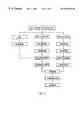
- FIG. 2is a flow diagram of the overall process at one level of generality.
- FIG. 3is a flow diagram of self-assembly processes.
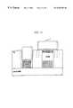
- FIG. 4Ais a perspective drawing of the apparatus and method for redistribution of photonic devices fabricated as dense arrays onto the host substrate without mother substrate layout constraints.
- FIG. 4Bis a perspective view of a clustering of nanospheres by DNA assisted self-assembly to form synthetic photonic crystals.
- FIG. 5is a plan view of the contact and lead portions of the target substrate or motherboard.
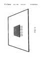
- FIG. 6is a cross-sectional view of a light emitting diode (LED) adapted to be transported through a fluidic medium to the target shown in FIG. 5 .
- LEDlight emitting diode
- FIG. 7is a plan view of a LED positioned adjacent locating electrodes.
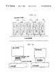
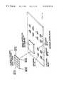
- FIGS. 8A, 8 B and 8 Cshow a motherboard and associated device for placement and attachment, including fluidic flow paths, FIGS. 8A and 8B showing flow paths from a drive electrode and FIG. 8C showing the flow path for the center electrode.
- FIG. 9is a perspective view of a flip-chip bonding arrangement which conserves the geometrical dimensions leading to the coupling of small dense arrays of specialty devices onto local regions of mother boards.
- FIG. 10shows a perspective view of global distribution of small dense structures from small dense chips on to less dense mother boards.
- FIG. 11shows a cross-sectional view of a structure for the self-assembly of micro or nanostructures utilizing a selective glue in which specialty devices of the given type are provided with a specific DNA polymer glue, the areas where these devices must attach being covered with the complimentary DNA glue.
- FIG. 12shows a cross-sectional view of selective electric field deposition of DNA onto the specially derivitized microelectrode surfaces.
- FIG. 13shows a cross-sectional view of a micro or nanoscale structure coupled to its host mother board substrate by selective DNA hybridization between complimentary DNA strands.
- FIG. 14shows a cross-sectional view of nanostructures held in place via a DNA bond (left-hand side) and nanostructure held by a metallurgical contact after a high temperature cycle (right-hand side).
- FIG. 15shows a cross-sectional view of an apparatus for the orientation of specialty devices prior to hybridization by physical masking and charge guiding.
- FIG. 16shows an apparatus for attachment and orientation of larger sized devices onto a substrate or motherboard.
- FIG. 17shows an apparatus for fabrication of nanostructures.
- Synthetic DNApossesses a number of important properties which make it a useful material for the applications of these inventions. The most important are the molecular recognition (via base pairing) and self-assembly (via hybridization) properties which are inherent in all DNA molecules. Other important advantages include the ability to easily synthesize DNA, and to readily modify its structure with a variety of functional groups. We have extensively investigated the photonic and electronic energy transfer mechanisms in self-assembled arrangements of synthetic DNA functionalized with a wide variety of donor and acceptor chromophore groups. We have paid particular attention to the basic problems involved in communicating or getting information in and out of these molecular structures.
- the DNA moleculeis considered important to certain aspects of this invention and the proposed applications because it is inherently programmable and can self-assemble. Designing, synthesizing, and organizing these systems requires nanometer range control which few other synthetic polymer systems can match. Additionally, DNA molecules are relatively stable and have a number of other attributes which make them a preferred material for nanofabrication.
- DNA polymershave three important advantages over any of the present polymeric materials used for electronic, and photonic applications.
- First, DNA polymersprovide a way to encode highly specific binding-site identities o semiconductor or photonic surfaces. These sites, produced at defined locations, could be of microscopic (micron), sub-micron, or even molecular (nanometer) dimension.
- Second, DNA polymersprovide a way to specifically connect any of these locations. The pre-programmed DNA polymers self-organize automatically.
- DNA polymersprovide the building blocks for nanotechnology; they are self-organizing materials for creating true molecular-level electronic and photonic devices.
- DNA polymersto be used to form programmable self-assembling structures.
- a photonic devicehas one specific DNA polymer sequence attached to it, it will only bind (hybridize) to a device or surface coated with the complementary DNA polymer sequence. Since a large variety of DNA sequences can be used, multiple devices, each attached to a different DNA sequence can in principle be self-assembled simultaneously. The following lists the important advantages of using DNA polymers for self-assembling nanofabrication applications:
- DNA polymerscan by synthesized both rapidly and efficiently with automated instruments. Conventional polymer chemistries can be significantly more complex and costly to develop.
- DNA polymerscan be synthesized in lengths from 2 to 150 nucleotides, which is the appropriate size range (1 nm to 60 nm) for self-assembling unit cells.
- DNA polymerscan be synthesized with any desired base sequence, therein providing programmable recognition for an almost unlimited number of specific connections.
- DNA polymers with unique sequences of as few as ten nucleotidesare highly specific and will bind only to their complementary sequence. Thus, the material allows specific connections as small as 3.4 nm to be made between molecular units.
- DNA polymerscan be covalently labeled with fluorophores, chromophores, affinity labels, metal chelates, chemically reactive functional groups and enzymes. This allows important photonic and electronic properties to be directly incorporated into the DNA polymers.
- DNA polymerscan be modified at any position in their sequence, and at several places within the individual nucleotide unit. This provides a means to position functional groups for maximum performance.
- DNA polymerscan be both covalently and non-covalently linked to solid surfaces: glass, metals, silicon, organic polymers, and bio-polymers. These attachment chemistries are both existing and easily developed.
- the backbone structure of the DNA molecule itselfcan be highly modified to produce different properties. Thus, there is compatibility with existing semiconductor and photonic substrate materials.
- Modified DNA polymerscan be used to form three-dimensional structures, thus leading to ultra high density secondary storage schemes.
- DNA polymerscan be reversibly assembled and disassembled by cooling and heating, or modified to remain in the assembled state. This is a critical property for self-organizing materials as it allows for more options in the manufacture of resulting systems.
- DNA polymersnucleic acids in general
- DNA polymersare well understood and can be easily modeled by simple computer programs. Thus, more complex molecular photonic and electronic devices can be designed.
- FIG. 2is a flow chart showing major components typically included in implementation of these inventions.
- the inventionsutilize the combination of fluidics and electronics for the transport and placement of a component device on a target device (sometimes referred to as a motherboard).
- Various modes of transport utilizing electronicstypically in a medium, most typically a fluid medium, include electrophoretic transport, electroosmotic transport, and dielectrophoretic action, including orientation and transport.
- Electrostatic potentialsmay be utilized with or without the presence of fluid.
- Electroosmotic transportis typically considered to be surface phenomenon, and accordingly, such transport is typically found close to the surface, most typically a charged surface, which results in a net fluid flow.
- FIG. 2identifies two primary components, a chip or motherboard 20 and a component device 22 .
- the chip or motherboard 20will include certain design aspects, described below, which aid in the achieving of the functions of placement, attachment and activation, if required, of the component device 22 .
- the component device 22is designed and fabricated to achieve the requirements of placement, attachment and activation, if required.
- the component device 22is delivered at step 24 to the vicinity of the chip or motherboard 20 .
- the component device 22may be delivered at step 24 in numerous ways, described below, though in the preferred embodiment, at least a portion of the delivery path includes a fluidic delivery portion.
- the placement step 26serves to position the component device 22 in proper relationship to the chip or motherboard 20 to permit the effective attachment and activation, if required, of the component device 22 .
- Attachment step 28may be achieved by any technique consistent with the other stated goals in functions of the invention, though in the preferred embodiment comprising a solder reflow technique. Namely, solder previously positioned on the chip or motherboard 20 , and/or the component device 22 may be made to form a electrical and mechanical attachment of the component device 22 to the chip/motherboard 20 . Additional mechanical attachment structures or forces may be utilized as necessary. If required by the nature of the device, activation step 30 serves to permit electronic interaction between the chip or motherboard 20 and component device 22 .
- FIG. 2includes certain specifics regarding the placement, attachment and activation of a light emitting diode (LED) as a component device 22 .
- a chip or motherboard 20may be designed and fabricated such that the LED component device 22 may be attached to it and made active through the operation of the chip or motherboard 20 .
- the LED component device 22is of a size (approximately 20 microns in diameter) and weight such that effective electrophoretic placement would not be feasible. Such transport would not be feasible if the charge to mass ratio necessary to effect electrophoretic transport was so high as to cause damage to the component device 22 , or could not be achieved through placement of charge on the component device 22 .
- electroosmotic flowmay be utilized, either alone or in combination with other forces (fluidic, electrostatic, electrophoretic and/or dielectrophoretic) in order to move the component device 22 relative to the chip or motherboard 20 to achieve the desired placement.
- forcesfluidic, electrostatic, electrophoretic and/or dielectrophoretic
- electrical attachmentmay be achieved, such as in the preferred embodiment by performing a solder reflow step 28 .
- provision of power from the chip or motherboard 20may result in LED activation.
- these inventionsrelate to methodologies, techniques, and devices which utilize self-assembling DNA polymers, modified DNA polymers, DNA derivitized structures and other affinity binding moieties for nanofabrication and microfabrication of electronic and photonic mechanisms, devices and systems.
- This inventionalso relates to processes which allow multiplex and multi-step fabrication, organization or assembly of modified DNA polymers, DNA derivitized structures, and other types of affinity or charged structures into more complex structures on or within silicon or other surfaces.
- DNA polymersis broadly defined as polymeric or oligomeric forms (linear or three-dimensional) of nucleic acids including: deoxyribonucleic acid, ribonucleic acids (synthetic or natural); peptide nucleic acids (PNA); methyphosphonates; and other forms of DNA in which the backbone structure has been modified to produce negative, positive or neutral species, or linkages other than the natural phosphate ester.
- nucleotide or polynucleotide unitsare interspersed with other units including but not limited to phosphate ester spacer moieties, amino acids, peptides, polysaccharides, synthetic organic polymers, silicon or inorganic polymers, conductive polymers, chromophoric polymers and nanoparticles or nanostructures.
- electroosmoticis broadly defined as an aspect of electrophoresis where the electric field causes the relative motion of water molecules and other entities to occur at or near a charged surface.
- electrosenoreticis broadly defined as a process for transporting electrically charged entities in solution using an electric field.
- dielectrophoreticis broadly defined as a process involving high frequency AC electric fields which causes the relative movement of molecules or other entities in solution.
- electrostaticis broadly defined as the net electric charge (positive or negative) on a molecule or other entity.
- Modified or Derivitized DNA polymersare broadly defined as nucleic acids which have been functionalized with chemical or biological moieties (e.g., amines, thiols, aldehydes, carboxyl groups, active esters, biotin and haptens) which allow the DNA to be attached covalently or non-covalently to other molecules, structures, or materials. Also included are forms of DNA which have been modified or Derivitized with chromophores, fluorophores, chelates, metal ions, amino acids, peptides, proteins, enzymes, antibodies, or aliphatic or aromatic moieties which change solubility, and moieties which change the net charge on the DNA molecule.
- chemical or biological moietiese.g., amines, thiols, aldehydes, carboxyl groups, active esters, biotin and haptens
- forms of DNAwhich have been modified or Derivitized with chromophores, fluorophores, chelates, metal
- DNA Derivitized structuresare broadly defined as nanostructures (organic, inorganic, biological); nanoparticles (gold, silica, and other inorganic materials); organic or polymeric nanobeads; submicron devices, components, particles, (silicon based devices produced by photolithography or E-beam lithography); and micron scale devices or particles which have been functionalized with a specific DNA sequence which allows the structure to be specifically attached or interconnected to another structure, device, or to a specific location on a surface.
- nanostructurerefers to sub-micron sized structures, terms such as “nano” or “micro” are not intended to be limited in the sense that a micron scale device can be functionalized with DNA polymers which technically have lengths of 10-180 nanometers.
- DNAprovides a programmable recognition code (via the DNA base sequence) which can be used for specific placement and alignment of sub-micron and nanoscale structures.
- the basic chemistry and technology required to attach specific DNA sequences to organic, semiconductor, and metallic compoundsis known to the art and specific chemistries are described for carrying out such applications.
- This fabrication techniquehas major applications in the field of optoelectronics and in the manufacturing of various hybrid-integrated components including flat panel displays, medical diagnostic equipment and data storage systems.
- Novel devices with very small physical dimensionstake advantage of various quantum confinement techniques. In most cases, these devices are preferably distributed over large areas (e.g. smart pixels and displays). Other devices may be brought together in dense regular crystal lattices (e.g. photonic bandgap crystals). In both cases, the physics of the devices are now understood, and viable fabrication techniques of these inventions are required. With regard to new processing techniques, DNA self-assembly technology allows these devices to be constructed.
- DNA self-assembly fabrication technologyinvolves the following steps. Synthetic DNA polymers are designed with highly specific binding affinities. When covalently attached to nanoscale organic, metallic or semiconductor component devices, DNA polymers provide a self-assembly fabrication mechanism. This mechanism can be used for both the selective grafting of devices to specific pre-programmed locations on a desired surface, and for the clustering of devices into pre-programmed 2 and 3 dimensional lattices.
- DNA polymers with complementary sequencesare first synthesized as shown in FIG. 2 .
- the photonic component devices and desired areas of the host substrate (receptor areas)are coated with the complementary DNA sequences.
- the host substrateis then introduced into a hybridization solution.
- the devices coated with the specific DNA polymersare also released from their mother substrate into the solution.
- the released devicescan be actively transported to their receptor areas under the influence of electrically or optically induced local fields (electrophoresis).
- Hybridizationis carried out by carefully controlling the solution temperature, ionic strength, or the electric field strength. Once the devices are grafted via hybridization to their specific receptor areas, the solution is removed and the substrate is dried.
- Metallurgical (or eutectic) bondingcan now be carried out at a higher temperature to fully bond the devices to the host substrate material.
- the clustering of sub-micron and nanoscale elements into 2-D or 3-D structurese.g., photonic band-gap crystals
- the host substrateis replaced by other nanoscale elements.
- the self-assembly fabrication technique based on DNA polymersoffers two unique features. First, by removing the requirement for conservation of relative device spacing (as defined by the mother substrate) during the device grafting (hybridization) process, the technique enables the micron, sub-micron or nanoscale devices to be fabricated densely on their mother substrates and then be redistributed in a preprogrammed fashion onto the host substrate (FIG. 4 A).
- the second featureis the ability to manipulate and orient with respect to each other a large number of nanoscale devices (e.g. organic or metallic nanospheres). This feature allows the “growth” of synthetic photonic crystals with large lattice constants possessing desired orientation symmetries for exhibiting photonic bandgap properties (FIG. 4 B).
- bonding structuressuch as gold, tin or solder structures as bonding pads, e.g., to achieve low cost or unassisted die-to-die processing, e.g., for flip-chip applications.
- these applicationsrequire four steps in the process.
- the firstinvolves the design and synthesis of the DNA polymer sequences and their selective attachment to the sub-micron and nanoscale devices of interest.
- Secondattachment of specific complementary DNA polymers to pre-selected receptor locations on a host substrate surface.
- Thirdthe self-assembly of the devices by the DNA hybridization process.
- the fourth processinvolves establishing the electrical contacts.
- This inventionbrings together molecular biological (DNA structure and function) and photonic and electronic device principles in a synergistic manner.
- novel deviceswith very small physical dimensions take advantage of various quantum confinement techniques. In most cases, these devices must be distributed over large areas (e.g. smart pixels and displays). In other cases, these devices must be brought together densely to form regular crystal lattices (e.g. photonic bandgap crystals).
- processing techniquesself-assembly DNA techniques with its well developed base of DNA synthesis, modification, and hybridization is an enabling technology for these applications.
- DNA linkage to solid supports and various other materialsis possible via a variety of processes for attaching DNA selectively to silicon, gold, aluminum and other inorganic and organic materials.
- a number of thin film processing techniquesare highly complementary with these DNA processes. For example, as will be described later, the lift-off process can be easily adapted to produce micron, and sub-micron devices with attached DNA sequences.
- FIG. 5is a plan view of the contacts and structures on the chip or motherboard.
- FIG. 6is a cross-sectional drawing of a component device LED adapted to be placed, attached, and activated through the contact structure of FIG. 5 .
- FIG. 5shows a generally planar structure having a first electrode 52 , second electrode 54 and lead 56 disposed on the surface or substrate 50 of the chip or motherboard.
- the first electrode 52is shown having a horseshoe shape, being an annularly shaped electrode being substantially continuous throughout the electrode region, and having two terminal ends.
- the second electrode 54may also be termed a center electrode or contact or anode contact. As shown, the center contact 54 is directly and electrically connected to lead 56 .
- Lead 56is disposed between, but spaced apart from, the terminal ends of the first electrode 52 .
- FIG. 6shows one implementation of a light emitting diode/component structure 60 .
- a substrate 62includes a first layer 64 disposed thereon, and a second layer 66 in contact with the first layer 64 . The interface between the first layer 64 and second layer 66 serve to generate light from the LED 60 . The light is generally emitted from the LED 60 in a downward direction as shown in FIG. 6 through the substrate 62 .
- a first electrode 68is disposed on the device 60 so as to contact the second layer 66 and first layer 64 .
- the first electrode 68is generally annular in shape and forms a continuous ring or band around the device 60 .
- the second electrode 70is disposed on the outward facing portion of the second layer 66 .
- the second electrode 70is of a circular disk-like shape.
- the second electrode 70comprises the anode contact for the P-region which constitutes the second layer 66 .
- the first electrode 68serves as the electrical contact for the first layer 64 which constitutes the end-region.
- the LED of FIG. 6When placed in an assembled condition, the LED of FIG. 6 is positioned such that the first electrode 68 in its annular portion disposed on the outward facing surface of the second layer 66 is in contact with the first electrode 52 of FIG. 5 .
- the second electrode 70contacts the center contact 54 on the substrate 50 .
- FIG. 7shows a microphotograph in plan view of a target site and LED.
- the LED 72is disposed above, and obscures, a center contact 54 and horseshoe shaped cathode 52 (previously described in connection with FIG. 5 ).
- Lead 74connects directly to the center contact 54 and lead 76 electrically contacts the center contact 54 and lead 76 electrically contacts the center contact.
- a first drive electrode 80is disposed proximal to the target location for the LED 72 .
- a second drive electrode 84is disposed in a mirror image relative to the transported device, that is, the LED 72 .
- the drive electrodes 80 , 84are contacted with a first drive electrode lead 82 and a second drive electrode lead 86 , respectively.
- each of the drive electrodes 80 , 84is quasi-kidney shaped. Alternate shapes consistent with the functionality of transport, placement and/or attachment may be utilized. For example, sections of an annular ring may be utilized.
- FIG. 8is a cross-sectional, diagrammatic view of an advantageous technique for the placement or positioning of a movable component device 90 .
- a host device or motherboard 92includes a surface 94 .
- the surface 94is generally disposed in an upward oriented configuration, and is adapted to receive the movable component device 90 .
- the surface 94is horizontally disposed, such that the movable component device 90 is subject to no or minimal lateral gravitational forces.
- the controllable electrical forcese.g., electroosmotic force, serves to place the movable component device 90 in the desired location.
- the surface 94receives the solution, typically a buffer solution, in which the movable component device 90 is placed.
- FIG. 8shows one advantageous mode of operation of a motherboard in order to place a movable component device 90 at a desired electrode location 96 .
- FIG. 8Ashows the movable component device 90 disposed above the surface 94 of the substrate 92 .
- the electroosmotic flow current 100is shown moving in a generally rightward direction on the surface 94 of the substrate 92 .
- a drive electrode 98is the active electrode for the creation of the electroosmotic current and flow 100 .
- the movable component device 90is subject to a lateral force in a rightward direction, causing its motion toward the target location, namely, the electrode location 96 .
- the electroosmotic flow 100 as it reaches the drive electrode 98is in a generally upward direction. As shown in FIG.
- FIG. 8Bshows an advantageous technique for the placement of the movable component device 90 more precisely on the electrode location 96 .
- the movable component devicecan be caused to be affirmatively pressed to the electrode 96 through the action of the electroosmotic flow and pressure generated therefrom. In this manner, the gross or rough positioning or placement of the movable component device 90 through action of the drive electrode 98 may be achieved, followed by the precise positioning of the movable component device 90 achieved through action of the electrode location 96 .
- the electrode array chipsundergo a O 2 plasma cleaning followed by a Ar plasma cleaning step (10 min each).
- the chipsare then placed in a medium sized plastic petri dish containing two droplets of water and about 100 ⁇ l of (Heptadecafluoro-1,1,2,2-tetrahydrodecyl)dimethylchlorosilane (Gelest).
- the petri dishis partially covered and evacuated (house vacuum) for about 15 min.
- the chipsare placed in a clean glass petri dish and cured at 90 C. for 15-30 min.
- the active electrode areais determined for each chip by running a cyclic voltamogramm (CV) in an aqueous solution of 0.1 M. K 2 K 3 Fe(CN) 6 and 0.5 M KCl and comparing with the CV obtained from a 80 ⁇ m circular electrode. The determined area is then used to calculate the necessary current corresponding to 3.75 ⁇ A on a 80 ⁇ m circular electrode.
- the chip surfaceis thoroughly rinsed with water and then covered with tin-lead (40:60) electroplating solution (Techni Solder Matte NF 820 HS, Technic Inc.) A constant current is applied for several seconds to produce the desired plating height. The plating solution is immediately removed and replaced by a 0.1M pH 5.2 sodium acetate buffer solution. Vigorous stirring is necessary to dissolve any precipitates.
- the chipsis thoroughly rinsed with water and air dried.
- the GaAs substrateis removed from the attached Si wafer by heating above 100 C. to melt the wax that is used for attachment.
- the freed GaAs waferis then soaked in dichloromethane for 15-45 min (to remove the wax), followed by a rinse with isopropanol and water. After drying the wafer is immersed in buffered HF (6:1) for 150 sec and then soaked in water. After drying the wafer is immersed in conc. HCl for 60 sec and then soaked in water. At this point usually a majority of the LEDs can be removed from their sockets with a micromanipulator tip.
- LEDs once lift-offtend to re-adhere strongly to the substrate over time. They can be re-released by short exposure (30 sec) to conc. HCl.
- Plasma cleaning(Ar or O 2 ) has no effect on the lift-off of LEDs. However, it has an impact on the behavior of LEDs in solution. Ar plasma cleaned LEDs adhere strongly to the SiO 2 chip surface and can hardly be flipped gold side down. Once flipped they tend to flip back very easily.
- New LEDsare first soaked in acetone followed by isopropanol and water and then air dried. Used LEDs are O 2 /Ar plasma cleaned (10+10 min). The cleaned LEDs (on their substrate) are immersed in 1-10% solutions of the respective thiol in 1:1 isopropanol/water for 60-120 min and then soaked in 1:1 isopropanol/water followed by water.
- the LEDsPrior to deposition the LEDs are O 2 plasma cleaned (10 min). Volatile silanes are deposited as vapors at ambient or reduced pressure for 15 min. Curing is performed at 90 C. for 15-30 min.
- Non-volatile silanesare deposited from 2% solutions in 200 proof ethanol (10 min). After deposition the samples are rinsed with ethanol and cured at 90 C. for 15-30 min.
- a water soluble glueis prepared by mixing 5-6 g of Ficol 400 into 2.5 ml glycol and 0.5 ml water. This mixture is very hygroscopic and relatively quickly changes its consistency. Ideally, the glue should stay at the tip of a fine micro-manipulator tip without wicking back by capillary force. LEDs are removed from their sockets with a clean probe tip. The very tip of the probe is brought in contact with the glue. A minimal amount of glue is used to pick-up and transfer the LED. The probe tip with the LED is moved to the surface of a dry chip. Water is added to the chip and the LED is released from the probe tip due to dissolution of the glue. The probe tip is removed and cleaned.
- the chipis rinsed 2 ⁇ with water, soaked for 1 min and then rinsed once more (Eppendorf pipette). After removal of the water, 10 mM aminocaproic acid solution is added to the chip. If the LED is oriented the wrong way, it can be flipped either by introducing turbulence with a probe tip or by moving the LED close to an electrode followed by application of a short pulse of current (100-200 nA).
- LEDs that are oriented with their gold contacts facing upwardstend to stick to the surface and do not move. If the gold contacts are facing towards the substrate surface the LEDs tend to hover and can be easily moved (electronically, by probe tip movement or by convection).
- a cathodic current(100-300 nA) is applied to one of the two drive electrodes (the one that is more distant from the LED) using the ring electrodes as counter electrodes.
- the currentis continuously adjusted to maintain a steady movement. (If the movement is too slow the LEDs can get stuck to the surface. If the movement is too fast the LEDs can get flipped in vicinity of the electrodes.)
- the second drive electrodeis activated without increasing the current. At this point current levels of about 10-30 nA should be sufficient to keep the LED close to the contact electrodes.
- the LEDis centered above the contact electrodes.
- the outer contact electrodeis activated as counter electrode while the ring electrodes are disconnected.
- the current (2-15 nA) now flowing between the drive electrodes and the outer contact electrodeforces the LED down onto the surface. If the LED is not sufficiently centered the previous step is reverted and then repeated. Immediately after this step the liquid is removed and the electrodes disconnected (over time larger currents are needed to keep the LED positioned).
- the LED/substrate assemblyis air dried and then exposed to an Ar plasma (ca. 250 W at 250 mTorr) for 10 min. This process physically attaches the LED to the contact electrodes.
- Ar plasmaca. 250 W at 250 mTorr
- a few microliters of flux(Alphametals 2491-121) are applied to the surface.
- the sampleis enclosed in a reflow chamber that is purged with a gentle flow of forming gas (95% N 2 , 5% H 2 ).
- the flux solventis dried off at 60 C. until the solid flux components precipitate.
- the sampleis then heated at a rate of about 90 C./min to a final temperature of 250 C. The heater is turned off and the forming gas flow is increased to let the sample cool down.
- One aspect of this inventionconcerns the potential to improve the performance of electric field assisted pick and place processes for heterogeneous integration under low gravity conditions.
- Low gravity conditionswould allow the pick the electric field assisted processes to be carried out under overall lower field conditions than under normal gravity.
- larger and heavier micron-scale objectscould now be transported, orientated, and positioned much more effectively then under normal gravity conditions.
- the electric field assisted processesmay prove more useful and viable when carried out in space platforms (space stations) were low gravity conditions exist.
- electric field assisted assembly under low gravity conditionsmay be carried out without the need for a fluidic environment, by using controlled electric fields to transport and manipulate objects which have an electrostatic charge.
- DNA sequencesare synthesized using automated DNA synthesizer and phosphoramidite chemistry procedures and reagents, using well known procedures.
- DNA polymerspolynucleotide, oligonucleotides, oligomers
- DNA polymerscan have primary amine groups incorporated at chemical bonding sites for subsequent attachment or functionalization reactions. These primary amine groups can be incorporated at precise locations on the DNA structure, according to the need for that particular sequence.
- Attachment sequencescan also contain a terminal ribonucleotide group for subsequent surface coupling reactions.
- Sequencesincluding the amino modified oligomers, can be purified by preparative gel electrophoresis (PAGE) or high pressure liquid chromatography (HPLC). Attachment sequences with terminal amino groups can be designed for covalent bonding to gold, silver, or aluminum metalized features or to small areas where silicon dioxide is present. These sequences can be further Derivitized with a thiolation reagent called succinimidyl 3-(2-pyridyldithio)propionate (SPDP). This particular reagent produces a sequence with a terminal sulfhydryl group which can be used for subsequent attachment to metal surfaces. Other attachment sequences containing a terminal ribonucleotide group can be converted to a dialdehyde derivative via Schiff s base reaction.
- SPDPsuccinimidyl 3-(2-pyridyldithio)propionate
- attachment sequencescan then be coupled to aminopropylated silicon dioxide surfaces.
- Specific sequences designed for electronic or photonic transfer responsescan be functionalized with their appropriate chromophore, fluorophore, or charge transfer groups. Many of these groups are available off-the-shelf as activated reagents that readily couple with the chemical bonding sites described above to form stable derivatives.
- This stepinvolves the covalent coupling of the attachment sequences to solid support materials.
- sequenceshave been covalently attached to a number of materials which include: (i) Glass (SiO 2 ), (ii) Silicon (Si), (iii) Metals (Gold, Silver, Aluminum), and (iv) Langmuir-Blodgett (LB) films.
- Glass, silicon, and aluminum structureshave been prepared in the following manner. Glass and silicon (SiO 2 ) are first treated with dilute sodium hydroxide solution and aluminum with dilute hydrogen fluoride solution. The materials are then Derivitized for covalent coupling with the attachment sequences by treatment with 3-aminopropyltriethoxysilane (APS).
- APS3-aminopropyltriethoxysilane
- a selective attachment procedure for the complementary DNA polymermay be carried out.
- the selective attachmentcan be realized by using the inherent selectivity of DNA sequences, selective attachment chemistries, or by directed electrophoretic transport. Alternatively after attachment, the DNA strands in unwanted regions can be destroyed by UV radiation. This approach is useful only when one group of devices need to be self-assembled. This approach would in normal operation preclude subsequent DNA attachment processes, and would not allow for the self-assembly of several specialty device groups. Attachment chemistry is strongly dependent upon the materials used to which the DNA polymers may be attached.
- the aluminum regionsare activated by dipping the sample for a short period of time into a dilute buffered HF solution.
- the end result of this processis that only a few DNA strands are attached to the protective glass layer while the exposed aluminum pads are highly reactive to DNA.
- This material selectivityis a convenient and general way to attach DNA to the desired regions. When material selectivity is combined with UV directed inactivation and electrophoretic transport, this allows for repeatable attachment processes to be carried out sequentially.
- each pad groupneeds to be coated with a specific DNA sequence complementary to the DNA sequence attached to the specialty device that it would be bonded to.
- each DNA sequenceis attached sequentially to the proper pads. This can be easily achieved by using the electrophoretic transport process and by applying a negative potential to the pads where DNA attachment is not desired. Simultaneously, a positive voltage can be applied to enhance attachment to the desired locations. Alternatively, an optically induced electric field can be used to migrate the DNA strands to desired locations. For a second set of DNA sequence attachment, the procedure is repeated. It should be pointed out that when only one type of device needs to be self-assembled on the host substrate, the use of the material selectivity of the DNA attachment chemistry alone is sufficient. UV radiation of the regions where DNA hybridization is not desired, would be carried out.
- Another key step for the self-assembly processis the preparation of the sub-micron and micron-scale component devices for DNA attachment, their handling during the attachment process, and their final release into solution prior to hybridization.
- the epitaxial lift-off (ELO) processcan substantially improve these aspects of this technique.
- Epitaxial films in the thickness range of 20 nm to 10 mmhave been separated from their growth substrates, handled and manipulated.
- thin III-V semiconductor filmshave been direct-bonded to foreign substrates, such as processed silicon wafers.
- Prior to lift-offvarious devices can be fabricated on the films while still on their mother substrates.
- the first step in our self-assembly techniqueis the preparation of the photonic devices that are to be grafted. FIG.
- the photonic devicesare fabricated in a standard fashion on their mother substrates on a sacrificial layer as required by the ELO process.
- a suitable coating layeris then deposited on these devices.
- the behavior of the devices once released into the saline solutioncan be controlled.
- the direction of the devices in the solutioncan be controlled.
- a thick polyamide filmis spun to provide a physical support to the devices after the ELO process.
- the ELO processis carried out and the thin film devices are separated from their mother substrates. By using plasma etching, the polyamide holding membrane is recessed in areas with no devices.
- a metal layercan be deposited to assure good electrical contacts to the photonic devices.
- the DNA attachment processis then carried out and a specific DNA sequence is covalently attached on all metal surfaces.
- the photonic devicesare used as a self-aligned mask enabling exposure of polyamide areas coated with DNA polymer. In these areas, the DNA polymers react to a form that is not suitable for further hybridization.
- the polyamidemay then be removed and the devices released into the saline solution used for the further hybridization processes.
- all devicesmay be released simultaneously into the solution.
- hybridization of the complementary DNA strandstakes place as the proper device-receptor pairs come into contact.
- the probability of hybridization taking placemay be related directly to the probability of the proper device-host pad pairs coming into contact. Since the probability distribution is most likely random, this process may take longer to achieve reasonable hybridization yields on large area surfaces unless the solution is saturated with the devices.
- several controlled heating and cooling cyclesmay be carried out during the hybridization process. During the heat cycle, weakly hybridized components are dissociated away to increase the chances of forming stronger bonds.
- the motherboard itself or another electrode array manufacturing deviceare used to produce localized electric fields which attract and concentrate selected component devices at selected locations.
- the motherboard or manufacturing devicehas sites which can be used as an electrodes.
- a potentialis applied across the solution between selected receptor sites and auxiliary electrodes.
- Receptor sites biased opposite (+) to the net charge ( ⁇ ) on selected devicesnow affect the electrophoretic transport and concentration of these devices thereby increasing the rate of hybridization and binding.
- These sitescan be selectively switched on or off using electronic or photonic addressing.
- a pulsing DC or biased AC electric fieldcan be applied at a suitable frequency to eliminate the screening effect of the unwanted device types.
- the electric field effectcan also be used in a protective manner.
- the receptor padsare now biased the same ( ⁇ ) as the net charge ( ⁇ ) on the devices.
- the devicesare then repelled from these regions and interact or bind only to those locations which have the opposite charge (+) or are neutral.
- Active electric field transportcan be used to carry out multiplex and multi-step addressing of component devices and structures to any location on the motherboard array.
- Another important consideration during hybridizationis the alignment accuracy of the photonic devices on the motherboard or host substrate. It is assumed cylindrical photonic devices that rotation is invariant. In this case, if the device and host pad diameter is d, an alignment accuracy of d/2 may be first achieved with the natural hybridization process prior to the drying process. Devices that are mis-aligned with more than d/2 misalignment will not form a strong bond during the hybridization process and will not be held in place during the heating and cooling cycles of the hybridization process. Better alignment accuracy and orientation are possible when active electric field hybridization is used. Once the substrates are removed from the solution, increased surface tension during the drying process could further improve the alignment accuracy.
- the specialty devicesare held in their proper places through the formation of the double-stranded DNA structure which has a very high bonding strength.
- the entire assemblyis then cleaned by rinsing and then dried.
- the DNA bond strengthremains in the solid state and serves to keep the devices in place.
- One method to achieve a metallurgical bond exhibiting an ohmic contact between the host substrate and the photonic devicesis to use conductive materials on the pads and devices that can be bonded together eutectically at low temperatures.
- a second methodis to use metals with low melting temperatures like solder or indium under a metal layer that is active for DNA attachment. While the photonic devices are held in place by the DNA bonds, the application of heat will result in the formation of a metallurgical bond.
- the DNA polymerwill disintegrate within the bond but may only contribute to an increased contact resistance depending on the initial DNA loading factor used.
- emitter arrayscan be advantageously formed.
- Specific DNA polymer sequencesmay be covalently attached to semiconductor light emitting diodes (LED) and the complementary DNA sequences may be attached to receptor pads on the host silicon substrate.
- UV/DNA patterning techniquesmay be used for selective activation/inactivation of DNA on the coated surfaces. All DNA Derivitized test structures and materials will then be tested for selective hybridizability using complementary fluorescent DNA probes. LED test devices Derivitized with specific DNA sequences may be hybridized to test substrates Derivitized with complementary DNA sequences.
- Photonic or crystalsmay be formed using the DNA self-assembly technique.
- Photonic Bandgap Structuresare artificial periodic lattice structures in two- or three-dimensional arrangements and composed of elements of proper dimensions, density and separations. Such structures result in the modification of photonic density of states and a gap in the electromagnetic wave dispersion. Indeed, photonic bandgap structures operating at specific optical wavelengths have been demonstrated. Potential applications of photonic bandgap materials include tailoring of the spontaneous emission of a laser to achieve ultra-low threshold lazing, improved wave guiding structures without radiation loss, novel optical modulators, etc.
- DNA polymer sequences described abovein the 20-mer to 50-mer size range, may be synthesized on automated DNA synthesizers using phosphoramidite chemistry.
- Longer DNA sequencesare generally required to bind larger objects to surfaces because the binding force must be sufficient to overcome forces (e.g., shearing forces) tending to remove the object.
- Longer DNA sequences(>50 mers) may be constructed using the polymerize chain reaction (PCR) technique.
- PCRpolymerize chain reaction
- the DNA sequencesmay be further Derivitized with appropriate functional groups (amines, thiols, aldehydes, fluorophores, etc.). All sequences may be purified by either PAGE gel electrophoresis or HPLC. After purification, all sequences may be checked on analytical PAGE gels for purity, and then tested for specificity by hybridization analysis.
- DNA sequencesmay be used to develop and test additional chemistries for the covalently attachment to various, organic polymer based nanospheres, semiconductor, and other material substrates (glass, gold, indium tin oxide, etc.). Additional attachment chemistries provide more options and flexibility for attachment selectivity to different semi-conductor materials.
- Specific DNA polymer sequencesmay be covalently attached to semi-conductor test structures and the complementary DNA sequences to test substrate (motherboard) materials. UV/DNA patterning techniques may be used for selective activation/inactivation of DNA on the coated surfaces. All DNA Derivitized test structures and materials will then be tested for selective hybridizability using complementary fluorescent DNA probes.
- Nanospheres, nanoparticles, and semi-conductor test structures Derivitized with specific DNA sequenceswill now be hybridized using both conventional (temperature, salt, and chaotropic agents) and electronic (electrophoretic) techniques to the test substrates (motherboards) Derivitized with complementary DNA sequences.
- the hybridization techniquesmay be optimized for highest selectivity and least amount of non-specific binding.
- Specific DNA polymer sequencesmay be covalently attached to semi-conductor light emitting diode (LED) component devices and the complementary DNA sequences to motherboard materials. UV/DNA patterning techniques may be used for selective activation/inactivation of DNA on the coated surfaces. LED component devices Derivitized with specific DNA sequences are then hybridized to test substrates (motherboards) Derivitized with complementary DNA sequences.
- LEDsemi-conductor light emitting diode
- Nanoparticles Derivitized with specific DNA sequenceswill now hybridized to the emitter test devices located on the substrates (motherboards) Derivitized with complementary DNA polymers.
- This inventionprovides for assembling specialty devices in parallel and over larger areas (up to several meters on a side) using a “self-assembly” technique.
- each device to be graftedsomehow “knows” where it is destined to be on the motherboard.
- This inventionrelates to a new integration technique based on programmable self-assembly principles encountered in biological systems. This new technique removes the requirement of dimension conservation during the grafting process.
- Our objectiveis to demonstrate the self-assembly of micro/nano structures on silicon using DNA (Deoxyribonucleic Acid) polymers as “selective glues”, thereby developing techniques for integrating these structures sparsely onto large area motherboards.
- This approachrelies on the principles of programmable self-assembly found in all biological systems, and uses existing well-understood synthetic DNA chemistry as the enabling process. These techniques include: 1) remove the specialty devices from their mother substrates using the epitaxial lift-off process, 2) attach selective DNA polymer sequences onto the specialty devices using DNA attachment chemistry specially developed in our company, 3) selectively attach complementary DNA polymer sequences to proper locations on the motherboard substrate, and 4) carry out self-assembly by using hybridization of the complementary DNA strands. This uses DNA polymer sequences as a smart and very selective glue to attach micron/nanosize specialty devices to designated areas on a motherboard (see FIG. 11 ).
- the secondis a method for electrophoretically transporting DNA-nanostructures (nanostructures to which specific DNA sequences are attached) to selected locations on substrate materials.
- the technique for UV lithography with DNAinvolves first coating a substrate material with a molecular layer of specific attachment DNA polymer sequences. An appropriate mask can be used to imprint a pattern into the attachment layer of DNA by exposure to UV irradiation (300 nm) for several seconds. The DNA in the area on the substrate exposed to UV light becomes in-active to hybridization with its complementary DNA sequence i.e., it is not able to form the double-stranded structure.
- FIG. 7show fluorescent DNA on a silicon structure was patterned with 10 micron lines using an electron microscope grid pattern.
- the first step in our self-assembly techniqueis the preparation of the specialty devices to grafting.
- the specialty devicesare fabricated in a standard fashion on their mother substrates on a sacrificial layer as required by the ELO process.
- a suitable coating layeris then deposited on these devices to assure they have a Brownian like motion in the saline solution.
- the behavior of the devices once released into the saline solutioncan be controlled. For example, by controlling the coating material properties we could control the direction of the devices in the solution.
- a thick polyamide filmmay be spun to provide a physical support to the devices after the ELO process.
- the ELO processmay be carried out and the thin film devices may be separated from their mother substrates.
- the polyamide filmmay be recessed to provide sufficient steps to prevent the metal layer from being continuous.
- the DNA attachment processis then carried out and a specific DNA sequence may be covalently attach on all the metal surfaces.
- the DNA areas that are exposed and not protectedmay be destroyed or put in a form that is not suitable for further hybridization.
- the polyamidewill then be removed and the devices may be released into the saline solution used for the further hybridization processes.
- a selective attachment procedure for the complementary DNA polymermust be carried out.
- the selective attachmentcan be realized by using the inherent selectivity of DNA sequences, selective attachment chemistries, or by directed electrophoretic transport. Alternatively after attachment, the DNA strands in unwanted regions can be destroyed by UV radiation. This approach is useful only when one group of devices need to be self-assembled.
- DNA attachment chemistryis strongly dependent on the materials used to which the DNA polymers may be attached.
- we first activate the aluminum regionsby dipping the sample for a short period of time into a dilute buffered HF solution.
- the end result of this processis that only a few DNA strands are attached to the protective glass layer while the exposed aluminum pads are highly reactive to DNA.
- This material selectivityis a convenient and general way to attach DNA to the desired regions. When material selectivity is combined with UV directed inactivation and electrophoretic transport process, this allows for repeatable attachment processes to be carried out sequentially. Consider the simultaneous self-assembly of several types of specialty devices.
- each pad groupneeds to be coated with a specific DNA sequence complementary to the DNA sequence attached to the specialty device that it would be bonded to.
- each DNA sequencecan be attached sequentially to the proper pads. This can be easily achieved by using the electrophoresis process and by applying a negative potential to the pads where DNA attachment is not desired. Simultaneously, a positive voltage can be applied to enhance attachment to the desired locations. For a second set of DNA sequence attachment, the procedure may be repeated with a different set of programming voltages.
- the motherboard receiving padsmay be programmed by applying a proper set of positive and negative potentials to the pads.
- the use of the material selectivity of the DNA attachment chemistry aloneis sufficient.
- the probability of a hybridization process taking placemay be related directly to the probability of the proper device-pad pairs to come into contact.
- the probability of a hybridization P hmay be roughly related to the ratio of the total available pad area A p to the mother board area A mb
- Nis the real density of one of the specialty device groups in the solution. Since the probability distribution is expected to be random, this process may take very long times to achieve reasonable hybridization yields. Alternatively it may require the solution to be saturated with the specialty devices. This may increase the cost of the process and limit the number of types of specialty devices that can be self-assembled. In order to improve the selectivity and alignment accuracy several heating and cooling cycles will be carried out during the hybridization process. During the heat cycle, weakly hybridized components may be dissociated away to increase the chance of forming stronger bonds.
- a key part of the self-assembly processis the preparation of the micro/nano scale devices for DNA attachment, their handling during the attachment and finally their release into the saline solution prior to hybridization.
- the most popular ELO approachis to employ the selectivity of dilute HF acid on the Al GaAs series of alloys.
- the Aluminum rich alloysetch at a rate of approximately 1 mm/hr, while the etch rate of Gallium rich alloys is almost undetectable, less than 0.1 nm/hr.
- An intermediate layer of AlAsdissolves, allowing upper epitaxial layers to simply float away from the substrate.
- Other separation methodshave also been used, including mechanical cleavage (CLEFT), and total substrate etching down to an etch stop layer.
- Epitaxial films in the thickness range between 20 nm and 10 mmhave been separated from their growth substrates, handled and manipulated.
- ELOis a true thin-film technology, allowing thin-film metal wiring which passes back and forth over the edge of a thin III-V film and onto a silicon micro-chip substrate. At the same time, the thin film is grown lattice-matched and essentially homo-epitaxially. Material quality, of the utmost importance for minority carrier devices such as light emitters, is never compromised.
- the ELOmay offer more in this aspect than the solder bump technique.
- ELO films grafting on processed silicon micro-circuitsrequires consideration of the ultra-fine scale roughness of the deposited oxide surfaces of the micro-chip. Surface roughness interferes with the quality of the Van der Waals or metallurgical bond.
- a second methodis to introduce each device group separately and to confine the specialty devices within regions near the positively biased pads. This confinement can be done under the influence of a DC electric field by applying a suitable positive voltage to the pads. The effect of the electric field can then be viewed as increasing the ratio of the areas, or equivalently increasing the device density, N, in the above equation.
- each device groupmust be introduced sequentially, so the unwanted device groups do not screen the right devices from reaching the pad.
- An alternative methodis to introduce all device types concurrently into the solution, to apply an initial DC voltage to create a distribution of the devices around each pad, and then to apply an AC voltage at a suitable frequency to eliminate the screening effect of the unwanted devices types.
- the effect of the AC fieldcan be seen as a stronger stirring mechanism.
- the specialty devicesare held in their proper places through the formation of the double-stranded DNA structure which has very high bonding strength.
- the entire assemblyis then cleaned by rinsing and then dried. At this point there is no electrical contact between the motherboard and the specialty devices.
- the DNA bond strengthremains in the solid state and serves to keep the devices in place.
- One method to achieve a metallurgical bond with ohmic contactis to use conductive materials on the pads and devices that can be bonded together eutectically at low temperatures.
- a second methodis to use metals with low melting temperatures like solder or indium under a metal layer that is active for DNA attachment. In this case the bumps must be made in nanometer dimensions.
- FIG. 14shows a the process described above.
- the devicesmay be self-aligned to the pads in a similar fashion as with the C4 technology used for flip-chip bonding.
Landscapes
- Chemical & Material Sciences (AREA)
- Engineering & Computer Science (AREA)
- Health & Medical Sciences (AREA)
- Physics & Mathematics (AREA)
- Life Sciences & Earth Sciences (AREA)
- Organic Chemistry (AREA)
- Biophysics (AREA)
- General Health & Medical Sciences (AREA)
- Molecular Biology (AREA)
- Nanotechnology (AREA)
- General Physics & Mathematics (AREA)
- Analytical Chemistry (AREA)
- Theoretical Computer Science (AREA)
- Biomedical Technology (AREA)
- Crystallography & Structural Chemistry (AREA)
- Biochemistry (AREA)
- Chemical Kinetics & Catalysis (AREA)
- Genetics & Genomics (AREA)
- Microelectronics & Electronic Packaging (AREA)
- Hematology (AREA)
- Immunology (AREA)
- Clinical Laboratory Science (AREA)
- Medicinal Chemistry (AREA)
- Mathematical Physics (AREA)
- Proteomics, Peptides & Aminoacids (AREA)
- Manufacturing & Machinery (AREA)
- General Engineering & Computer Science (AREA)
- Artificial Intelligence (AREA)
- Spectroscopy & Molecular Physics (AREA)
- Software Systems (AREA)
- Condensed Matter Physics & Semiconductors (AREA)
- Computational Linguistics (AREA)
- Data Mining & Analysis (AREA)
- Evolutionary Computation (AREA)
- Computing Systems (AREA)
- Dispersion Chemistry (AREA)
- Biotechnology (AREA)
- Bioinformatics & Cheminformatics (AREA)
- Bioinformatics & Computational Biology (AREA)
- Power Engineering (AREA)
Abstract
Description
Claims (12)
Priority Applications (15)
| Application Number | Priority Date | Filing Date | Title |
|---|---|---|---|
| US09/436,311US6569382B1 (en) | 1991-11-07 | 1999-11-08 | Methods apparatus for the electronic, homogeneous assembly and fabrication of devices |
| US09/489,855US6706473B1 (en) | 1996-12-06 | 2000-01-24 | Systems and devices for photoelectrophoretic transport and hybridization of oligonucleotides |
| DK00976960.5TDK1230340T3 (en) | 1999-11-08 | 2000-11-03 | Methods for electronic, homogeneous assembly and manufacturing of appliances |
| KR1020027005963AKR20030014345A (en) | 1999-11-08 | 2000-11-03 | Methods and apparatus for the electronic, homogeneous assembly and fabrication of devices |
| AT00976960TATE517173T1 (en) | 1999-11-08 | 2000-11-03 | METHOD FOR ELECTRONIC, HOMOGENEOUS ASSEMBLY AND MANUFACTURING OF OBJECTS |
| JP2001537462AJP4334798B2 (en) | 1999-11-08 | 2000-11-03 | Methods for electroosmotic transport and bonding of microscale and nanoscale component devices |
| AU14662/01AAU1466201A (en) | 1999-11-08 | 2000-11-03 | Methods and apparatus for the electronic, homogeneous assembly and fabrication of devices |
| EP00976960AEP1230340B1 (en) | 1999-11-08 | 2000-11-03 | Methods for the electronic, homogeneous assembly and fabrication of devices |
| PT00976960TPT1230340E (en) | 1999-11-08 | 2000-11-03 | METHODS FOR THE ASSEMBLY AND HOMOGENEOUS DEVICE ASSEMBLY AND MANUFACTURING |
| PCT/US2000/030480WO2001034765A1 (en) | 1999-11-08 | 2000-11-03 | Methods and apparatus for the electronic, homogeneous assembly and fabrication of devices |
| CA2389314ACA2389314C (en) | 1999-11-08 | 2000-11-03 | Methods and apparatus for the electronic, homogeneous assembly and fabrication of devices |
| ES00976960TES2370081T3 (en) | 1999-11-08 | 2000-11-03 | METHODS FOR HOMOGENICAL, ELECTRONIC ASSEMBLY AND DEVICE MANUFACTURING. |
| US10/337,450US7060224B2 (en) | 1999-11-08 | 2003-01-06 | Methods for the electronic, homogeneous assembly and fabrication of devices |
| US10/772,744US20040209355A1 (en) | 1996-12-06 | 2004-02-04 | Systems and devices for photoelectrophoretic transport and hybridization of oligonucleotides |
| US11/401,713US8630807B2 (en) | 1993-11-01 | 2006-04-11 | Methods for the electronic, homogeneous assembly and fabrication of devices |
Applications Claiming Priority (14)
| Application Number | Priority Date | Filing Date | Title |
|---|---|---|---|
| US79026291A | 1991-11-07 | 1991-11-07 | |
| US08/232,233US5565322A (en) | 1991-11-07 | 1992-11-06 | Hybridization of polynucleotides conjugated with chromophores and fluorophores to generate donor-to donor energy transfer system |
| US08/146,504US5605662A (en) | 1993-11-01 | 1993-11-01 | Active programmable electronic devices for molecular biological analysis and diagnostics |
| US08/258,168US5787032A (en) | 1991-11-07 | 1994-06-10 | Deoxyribonucleic acid(DNA) optical storage using non-radiative energy transfer between a donor group, an acceptor group and a quencher group |
| US08/271,882US6017696A (en) | 1993-11-01 | 1994-07-07 | Methods for electronic stringency control for molecular biological analysis and diagnostics |
| US08/304,657US5632957A (en) | 1993-11-01 | 1994-09-09 | Molecular biological diagnostic systems including electrodes |
| US08/534,454US5849486A (en) | 1993-11-01 | 1995-09-27 | Methods for hybridization analysis utilizing electrically controlled hybridization |
| US08/703,601US5849489A (en) | 1991-11-07 | 1996-08-23 | Hybridization of polynucleotides conjugated with chromophores and fluorophores to generate donor-to-donor energy transfer system |
| US08/760,933US6652808B1 (en) | 1991-11-07 | 1996-12-06 | Methods for the electronic assembly and fabrication of devices |
| US08/855,058US6048690A (en) | 1991-11-07 | 1997-05-14 | Methods for electronic fluorescent perturbation for analysis and electronic perturbation catalysis for synthesis |
| US08/906,569US5835404A (en) | 1991-11-07 | 1997-08-05 | DNA optical storage device utilizing non-radiative energy transfer |
| US08/986,065US6051380A (en) | 1993-11-01 | 1997-12-05 | Methods and procedures for molecular biological analysis and diagnostics |
| US09/129,740US6067246A (en) | 1991-11-07 | 1998-08-05 | Method for writing data to and reading multiple bit data words from a DNA optical storage device |
| US09/436,311US6569382B1 (en) | 1991-11-07 | 1999-11-08 | Methods apparatus for the electronic, homogeneous assembly and fabrication of devices |
Related Parent Applications (3)
| Application Number | Title | Priority Date | Filing Date |
|---|---|---|---|
| US08/703,601Continuation-In-PartUS5849489A (en) | 1991-11-07 | 1996-08-23 | Hybridization of polynucleotides conjugated with chromophores and fluorophores to generate donor-to-donor energy transfer system |
| US08/760,933Continuation-In-PartUS6652808B1 (en) | 1991-11-07 | 1996-12-06 | Methods for the electronic assembly and fabrication of devices |
| US09/129,470Continuation-In-PartUS6329143B1 (en) | 1989-06-07 | 1998-08-04 | Very large scale immobilized polymer synthesis |
Related Child Applications (4)
| Application Number | Title | Priority Date | Filing Date |
|---|---|---|---|
| US08/232,233Continuation-In-PartUS5565322A (en) | 1991-11-07 | 1992-11-06 | Hybridization of polynucleotides conjugated with chromophores and fluorophores to generate donor-to donor energy transfer system |
| US08/271,882Continuation-In-PartUS6017696A (en) | 1991-11-07 | 1994-07-07 | Methods for electronic stringency control for molecular biological analysis and diagnostics |
| US09/489,855Continuation-In-PartUS6706473B1 (en) | 1996-12-06 | 2000-01-24 | Systems and devices for photoelectrophoretic transport and hybridization of oligonucleotides |
| US10/337,450ContinuationUS7060224B2 (en) | 1993-11-01 | 2003-01-06 | Methods for the electronic, homogeneous assembly and fabrication of devices |
Publications (1)
| Publication Number | Publication Date |
|---|---|
| US6569382B1true US6569382B1 (en) | 2003-05-27 |
Family
ID=23731946
Family Applications (3)
| Application Number | Title | Priority Date | Filing Date |
|---|---|---|---|
| US09/436,311Expired - Fee RelatedUS6569382B1 (en) | 1991-11-07 | 1999-11-08 | Methods apparatus for the electronic, homogeneous assembly and fabrication of devices |
| US10/337,450Expired - LifetimeUS7060224B2 (en) | 1993-11-01 | 2003-01-06 | Methods for the electronic, homogeneous assembly and fabrication of devices |
| US11/401,713Expired - Fee RelatedUS8630807B2 (en) | 1993-11-01 | 2006-04-11 | Methods for the electronic, homogeneous assembly and fabrication of devices |
Family Applications After (2)
| Application Number | Title | Priority Date | Filing Date |
|---|---|---|---|
| US10/337,450Expired - LifetimeUS7060224B2 (en) | 1993-11-01 | 2003-01-06 | Methods for the electronic, homogeneous assembly and fabrication of devices |
| US11/401,713Expired - Fee RelatedUS8630807B2 (en) | 1993-11-01 | 2006-04-11 | Methods for the electronic, homogeneous assembly and fabrication of devices |
Country Status (11)
| Country | Link |
|---|---|
| US (3) | US6569382B1 (en) |
| EP (1) | EP1230340B1 (en) |
| JP (1) | JP4334798B2 (en) |
| KR (1) | KR20030014345A (en) |
| AT (1) | ATE517173T1 (en) |
| AU (1) | AU1466201A (en) |
| CA (1) | CA2389314C (en) |
| DK (1) | DK1230340T3 (en) |
| ES (1) | ES2370081T3 (en) |
| PT (1) | PT1230340E (en) |
| WO (1) | WO2001034765A1 (en) |
Cited By (58)
| Publication number | Priority date | Publication date | Assignee | Title |
|---|---|---|---|---|
| US20020183996A1 (en)* | 2000-06-27 | 2002-12-05 | Fluidigm Corporation | Computer aided design method and system for developing a microfluidic system |
| US20030072519A1 (en)* | 2001-10-17 | 2003-04-17 | Bolanos Miguel Holgado | Photonic device, optical logic circuit incorporting the photonic device and method of manufacturing thereof |
| US20030146095A1 (en)* | 1999-11-08 | 2003-08-07 | Nanogen, Inc. | Methods for the electronic, Homogeneous assembly and fabrication of devices |
| US20030204369A1 (en)* | 2002-04-30 | 2003-10-30 | Hamlin Christopher L. | Collaborative integration of hybrid electronic and micro and sub-micro level aggregates |
| US20040115696A1 (en)* | 1996-12-06 | 2004-06-17 | Nanotronics, Inc. | Affinity based self-assembly systems and devices for photonic and electronic applications |
| US20040209355A1 (en)* | 1996-12-06 | 2004-10-21 | Nanogen, Inc. | Systems and devices for photoelectrophoretic transport and hybridization of oligonucleotides |
| US20040217345A1 (en)* | 2003-05-01 | 2004-11-04 | Clemson University | DNA-based memory device and method of reading and writing same |
| US20050019792A1 (en)* | 2001-11-30 | 2005-01-27 | Fluidigm Corporation | Microfluidic device and methods of using same |
| US20050053952A1 (en)* | 2002-10-02 | 2005-03-10 | California Institute Of Technology | Microfluidic nucleic acid analysis |
| US20050129581A1 (en)* | 2003-04-03 | 2005-06-16 | Fluidigm Corporation | Microfluidic devices and methods of using same |
| US20050215067A1 (en)* | 2004-03-26 | 2005-09-29 | Kiyotaka Mori | Combination insulator and organic semiconductor formed from self-assembling block co-polymers |
| US20050218398A1 (en)* | 2004-04-06 | 2005-10-06 | Availableip.Com | NANO-electronics |
| US20050252773A1 (en)* | 2003-04-03 | 2005-11-17 | Fluidigm Corporation | Thermal reaction device and method for using the same |
| US20060014151A1 (en)* | 2002-12-25 | 2006-01-19 | Jun Ogura | Optical dna sensor, dna reading apparatus, identification method of dna and manufacturing method of optical dna sensor |
| US20060048384A1 (en)* | 2004-09-03 | 2006-03-09 | Eastman Kodak Company | Thermally controlled fluidic self-assembly and conductive support |
| US20060099116A1 (en)* | 2000-10-13 | 2006-05-11 | Mycometrix Corporation | Microfluidic-based electrospray source for analytical devices |
| US20060210993A1 (en)* | 2005-02-23 | 2006-09-21 | Aref Chowdhury | DNA structures on ferroelectrics and semiconductors |
| US20070138024A1 (en)* | 2004-09-21 | 2007-06-21 | Swanson Paul D | Electrode based patterning of thin film self-assembled nanoparticles |
| KR100808966B1 (en) | 2000-07-25 | 2008-03-04 | 더블유엠. 마쉬 라이스 유니버시티 | Programmable Molecular Devices |
| US20080119371A1 (en)* | 2002-06-20 | 2008-05-22 | Affymetrix, Inc. | Antireflective coatings for high-resolution photolithographic synthesis of dna arrays |
| US20080157786A1 (en)* | 2006-12-28 | 2008-07-03 | Gordon Holt | Quality control methods for the manufacture of polymer arrays |
| US20080176762A1 (en)* | 2007-01-24 | 2008-07-24 | Arrayomics, Inc. | Microdevice Arrays Formed by Magnetic Assembly |
| US7413712B2 (en) | 2003-08-11 | 2008-08-19 | California Institute Of Technology | Microfluidic rotary flow reactor matrix |
| US7452726B2 (en) | 2002-04-01 | 2008-11-18 | Fluidigm Corporation | Microfluidic particle-analysis systems |
| US7476363B2 (en) | 2003-04-03 | 2009-01-13 | Fluidigm Corporation | Microfluidic devices and methods of using same |
| US20090093381A1 (en)* | 2006-12-28 | 2009-04-09 | Wei Wang | Solid phase electrochemical synthesis with controlled product cleavage |
| US20090236310A1 (en)* | 2005-04-14 | 2009-09-24 | Vincent Linder | Adjustable solubility in sacrificial layers for microfabrication |
| US7820427B2 (en) | 2001-11-30 | 2010-10-26 | Fluidigm Corporation | Microfluidic device and methods of using same |
| US7833708B2 (en) | 2001-04-06 | 2010-11-16 | California Institute Of Technology | Nucleic acid amplification using microfluidic devices |
| CN101400599B (en)* | 2006-03-10 | 2010-12-01 | 松下电器产业株式会社 | Mounting method of anisotropic shape parts |
| US7867454B2 (en) | 2003-04-03 | 2011-01-11 | Fluidigm Corporation | Thermal reaction device and method for using the same |
| US20110035043A1 (en)* | 2009-08-07 | 2011-02-10 | Taiwan Semiconductor Manufacturing Company, Ltd. | Method and apparatus for wireless transmission of diagnostic information |
| US8105821B2 (en) | 2002-06-20 | 2012-01-31 | Affymetrix, Inc. | Silane mixtures |
| US8440093B1 (en) | 2001-10-26 | 2013-05-14 | Fuidigm Corporation | Methods and devices for electronic and magnetic sensing of the contents of microfluidic flow channels |
| DE102006016275B4 (en)* | 2006-03-31 | 2013-12-19 | Asm Assembly Systems Gmbh & Co. Kg | Method for placing electrically contactable components on a circuit carrier |
| US8658418B2 (en) | 2002-04-01 | 2014-02-25 | Fluidigm Corporation | Microfluidic particle-analysis systems |
| US8828663B2 (en) | 2005-03-18 | 2014-09-09 | Fluidigm Corporation | Thermal reaction device and method for using the same |
| US8961764B2 (en) | 2010-10-15 | 2015-02-24 | Lockheed Martin Corporation | Micro fluidic optic design |
| US9067207B2 (en) | 2009-06-04 | 2015-06-30 | University Of Virginia Patent Foundation | Optical approach for microfluidic DNA electrophoresis detection |
| US9322054B2 (en) | 2012-02-22 | 2016-04-26 | Lockheed Martin Corporation | Microfluidic cartridge |
| US9714443B2 (en) | 2002-09-25 | 2017-07-25 | California Institute Of Technology | Microfabricated structure having parallel and orthogonal flow channels controlled by row and column multiplexors |
| WO2018217284A1 (en)* | 2017-05-26 | 2018-11-29 | Nlight, Inc. | Multi-function semiconductor and electronics processing |
| US10434600B2 (en) | 2015-11-23 | 2019-10-08 | Nlight, Inc. | Fine-scale temporal control for laser material processing |
| US10486153B2 (en) | 2013-09-27 | 2019-11-26 | Illumina, Inc. | Method to produce chemical pattern in micro-fluidic structure |
| US10520671B2 (en) | 2015-07-08 | 2019-12-31 | Nlight, Inc. | Fiber with depressed central index for increased beam parameter product |
| US10535973B2 (en) | 2015-01-26 | 2020-01-14 | Nlight, Inc. | High-power, single-mode fiber sources |
| US10649241B2 (en) | 2016-09-29 | 2020-05-12 | Nlight, Inc. | Multi-function semiconductor and electronics processing |
| US10656330B2 (en) | 2016-09-29 | 2020-05-19 | Nlight, Inc. | Use of variable beam parameters to control solidification of a material |
| US10730785B2 (en) | 2016-09-29 | 2020-08-04 | Nlight, Inc. | Optical fiber bending mechanisms |
| USRE48219E1 (en) | 2008-05-05 | 2020-09-22 | Illumina, Inc. | Compensator for multiple surface imaging |
| US10838939B2 (en)* | 2016-10-28 | 2020-11-17 | Integrated Dna Technologies, Inc. | DNA data storage using reusable nucleic acids |
| US10971885B2 (en) | 2014-06-02 | 2021-04-06 | Nlight, Inc. | Scalable high power fiber laser |
| US10971884B2 (en) | 2015-03-26 | 2021-04-06 | Nlight, Inc. | Fiber source with cascaded gain stages and/or multimode delivery fiber with low splice loss |
| US11008644B2 (en) | 2013-02-21 | 2021-05-18 | Nlight, Inc. | Laser patterning of multi-layer structures |
| US11179807B2 (en) | 2015-11-23 | 2021-11-23 | Nlight, Inc. | Fine-scale temporal control for laser material processing |
| EP3899543A4 (en)* | 2018-12-17 | 2022-08-17 | Illumina, Inc. | FLOW CELL AND SEQUENCING KIT |
| US12083514B2 (en) | 2018-07-03 | 2024-09-10 | Illumina, Inc. | Interposer with first and second adhesive layers |
| US12390810B2 (en) | 2019-08-23 | 2025-08-19 | The Regents Of The University Of California | Electrokinetic microelectrode devices and methods for biomarker analysis |
Families Citing this family (36)
| Publication number | Priority date | Publication date | Assignee | Title |
|---|---|---|---|---|
| US6780696B1 (en) | 2000-09-12 | 2004-08-24 | Alien Technology Corporation | Method and apparatus for self-assembly of functional blocks on a substrate facilitated by electrode pairs |
| GB0205455D0 (en) | 2002-03-07 | 2002-04-24 | Molecular Sensing Plc | Nucleic acid probes, their synthesis and use |
| EP1509816B1 (en)* | 2002-05-21 | 2012-12-26 | Northwestern University | Electrostatically driven lithography |
| US20070157873A1 (en)* | 2003-09-12 | 2007-07-12 | Hauptmann Jonas R | Method of fabrication and device comprising elongated nanosize elements |
| JP4321854B2 (en)* | 2003-10-02 | 2009-08-26 | ソニー株式会社 | Hybridization and other interaction detection units and DNA chips and other bioassay substrates provided with the detection units |
| US7612370B2 (en)* | 2003-12-31 | 2009-11-03 | Intel Corporation | Thermal interface |
| US7862624B2 (en)* | 2004-04-06 | 2011-01-04 | Bao Tran | Nano-particles on fabric or textile |
| US7019391B2 (en)* | 2004-04-06 | 2006-03-28 | Bao Tran | NANO IC packaging |
| US7330369B2 (en)* | 2004-04-06 | 2008-02-12 | Bao Tran | NANO-electronic memory array |
| US20050218397A1 (en)* | 2004-04-06 | 2005-10-06 | Availableip.Com | NANO-electronics for programmable array IC |
| JP2006047153A (en)* | 2004-08-05 | 2006-02-16 | Sony Corp | Manufacturing method and manufacturing system of dna chip, detection method and detection system of hybridization, and substrate processing device and substrate processing method |
| US7671398B2 (en)* | 2005-02-23 | 2010-03-02 | Tran Bao Q | Nano memory, light, energy, antenna and strand-based systems and methods |
| WO2006110846A2 (en)* | 2005-04-08 | 2006-10-19 | Abeygunaratne Thusara Sugat Ch | Method and device for probing changes in a membrane by applying an in-plane electric field |
| CN100417117C (en)* | 2005-06-15 | 2008-09-03 | 华为技术有限公司 | Recognition Method of Node Reachability in Automatic Switched Optical Network |
| JP2008545264A (en)* | 2005-07-05 | 2008-12-11 | コーニンクレッカ フィリップス エレクトロニクス エヌ ヴィ | Packaged semiconductor sensor chip for use in liquids |
| GB0516278D0 (en)* | 2005-08-08 | 2005-09-14 | Xaar Technology Ltd | Device and method of forming a device |
| WO2007088406A1 (en)* | 2006-02-01 | 2007-08-09 | Alma Mater Studiorum- Universita'di Bologna | Use of dna or fragments or analogs thereof as a molecular glue |
| US7393699B2 (en) | 2006-06-12 | 2008-07-01 | Tran Bao Q | NANO-electronics |
| US7803588B2 (en)* | 2006-09-07 | 2010-09-28 | Abeygunaratne Thusara Sugat Chandra | Method and device to probe a membrane by applying an in-plane electric field |
| US7892719B2 (en)* | 2006-11-03 | 2011-02-22 | Intel Corporation | Photonic crystal EUV photoresists |
| US20090077553A1 (en)* | 2007-09-13 | 2009-03-19 | Jian Tang | Parallel processing of platform level changes during system quiesce |
| WO2009055862A1 (en)* | 2007-11-01 | 2009-05-07 | Newsouth Innovations Pty Limited | Method of component assembly on a substrate |
| US8722437B2 (en) | 2007-11-01 | 2014-05-13 | Mogul Solutions Llc | Method of component assembly on a substrate |
| US8049183B1 (en) | 2007-11-09 | 2011-11-01 | Carnegie Mellon University | Apparatuses and methods for control and self-assembly of particles into adaptable monolayers |
| US9551026B2 (en) | 2007-12-03 | 2017-01-24 | Complete Genomincs, Inc. | Method for nucleic acid detection using voltage enhancement |
| EP2414800A1 (en)* | 2009-03-31 | 2012-02-08 | FemtoTools GmbH | Micro force sensor package for sub-millinewton electromechanical measurements |
| US8828246B2 (en)* | 2010-02-18 | 2014-09-09 | Anpac Bio-Medical Science Co., Ltd. | Method of fabricating micro-devices |
| EP2625522B1 (en)* | 2010-10-05 | 2019-09-25 | ANPAC Bio-Medical Science Co., Ltd. | Micro-devices for disease detection |
| CN103562728B (en) | 2011-03-24 | 2016-08-17 | 安派科生物医学科技有限公司 | Micro element for disease detection |
| US10837879B2 (en) | 2011-11-02 | 2020-11-17 | Complete Genomics, Inc. | Treatment for stabilizing nucleic acid arrays |
| EP2867018B1 (en)* | 2012-06-29 | 2019-05-01 | Northeastern University | Three-dimensional hybrid nanostructures fabricated by electric field directed assembly of nanoelements |
| US10039194B2 (en) | 2012-08-02 | 2018-07-31 | Osram Sylvania Inc. | Dual solder layer for fluidic self assembly and electrical component substrate and method employing same |
| US10014261B2 (en) | 2012-10-15 | 2018-07-03 | Palo Alto Research Center Incorporated | Microchip charge patterning |
| US9275871B2 (en) | 2014-01-09 | 2016-03-01 | Micron Technology, Inc. | Nanostructures having low defect density and methods of forming thereof |
| US9739751B2 (en) | 2015-02-05 | 2017-08-22 | International Business Machines Corporation | Devices for trapping and controlling microparticles with radiation |
| CN107922182A (en)* | 2015-06-08 | 2018-04-17 | 查尔斯·斯塔克·德雷珀实验室公司 | Nanoscale and micrometric objects are assembled into the method for three-dimensional structure |
Citations (66)
| Publication number | Priority date | Publication date | Assignee | Title |
|---|---|---|---|---|
| US3950738A (en) | 1973-07-13 | 1976-04-13 | Agency Of Industrial Science & Technology | Semi-conductor non-volatile optical memory device |
| US3995190A (en) | 1974-09-19 | 1976-11-30 | Butler, Binion, Rice, Cook & Knapp | Mobile ion film memory |
| US4032901A (en) | 1975-02-12 | 1977-06-28 | Cyrus Levinthal | System for storing and retrieving information at the molecular level |
| GB2156074A (en) | 1984-02-17 | 1985-10-02 | Orion Yhtymae Oy | Improved nucleic acid reagents and methods for their preparation |
| US4563419A (en) | 1981-10-16 | 1986-01-07 | Orion Corporation Ltd. | Detection of microbial nucleic acids by a one-step sandwich hybridization test |
| US4580895A (en) | 1983-10-28 | 1986-04-08 | Dynatech Laboratories, Incorporated | Sample-scanning photometer |
| US4584075A (en) | 1984-11-26 | 1986-04-22 | Ionics Incorporated | Process and apparatus for electrically desorbing components selectively sorbed on an electrolytically conducting barrier |
| US4594135A (en) | 1985-02-20 | 1986-06-10 | Ionics Incorporated | Process and apparatus for electrically desorbing components selectively sorbed on granules |
| WO1986003782A1 (en) | 1984-12-19 | 1986-07-03 | Blair Malcolm A D | Improved sandwich hybridisation technique for the detection of nucleotide sequences |
| EP0228075A2 (en) | 1986-01-03 | 1987-07-08 | Molecular Diagnostics, Inc. | Eucaryotic genomic dna dot-blot hybridization method |
| US4728724A (en) | 1985-04-08 | 1988-03-01 | Hoechst Celanese Corporation | Optical data storage medium comprising a chromophore/polymer information layer |
| US4751177A (en) | 1985-06-13 | 1988-06-14 | Amgen | Methods and kits for performing nucleic acid hybridization assays |
| WO1988008528A1 (en) | 1987-05-01 | 1988-11-03 | Biotronic Systems Corporation | Added array of molecular chains for interfering with electrical fields |
| US4787963A (en) | 1987-05-04 | 1988-11-29 | Syntro Corporation | Method and means for annealing complementary nucleic acid molecules at an accelerated rate |
| WO1989001159A1 (en) | 1987-07-27 | 1989-02-09 | Commonwealth Scientific And Industrial Research Or | Receptor membranes |
| US4804625A (en) | 1984-09-27 | 1989-02-14 | Amoco Corporation | Assay procedures |
| US4816418A (en) | 1985-07-22 | 1989-03-28 | Sequoia-Turner Corporation | Method and apparatus for performing automated, multi-sequential immunoassays |
| US4822566A (en) | 1985-11-19 | 1989-04-18 | The Johns Hopkins University | Optimized capacitive sensor for chemical analysis and measurement |
| US4822746A (en) | 1986-06-25 | 1989-04-18 | Trustees Of Tufts College | Radiative and non-radiative energy transfer and absorbance modulated fluorescence detection methods and sensors |
| US4824776A (en) | 1985-07-25 | 1989-04-25 | Molecular Biosystems, Inc. | Method for increasing the sensitivity of nucleic acid hybridization assays |
| US4859583A (en) | 1985-02-25 | 1989-08-22 | Amoco Corporation | Chemiluminescent immunochemical technique for low molecular weight antigens |
| US4868103A (en) | 1986-02-19 | 1989-09-19 | Enzo Biochem, Inc. | Analyte detection by means of energy transfer |
| WO1989010977A1 (en) | 1988-05-03 | 1989-11-16 | Isis Innovation Limited | Analysing polynucleotide sequences |
| WO1990001564A1 (en) | 1988-08-09 | 1990-02-22 | Microprobe Corporation | Methods for multiple target analyses through nucleic acid hybridization |
| US4908112A (en) | 1988-06-16 | 1990-03-13 | E. I. Du Pont De Nemours & Co. | Silicon semiconductor wafer for analyzing micronic biological samples |
| US4996143A (en) | 1985-12-23 | 1991-02-26 | Syngene, Inc. | Fluorescent stokes shift probes for polynucleotide hybridization |
| EP0229943B1 (en) | 1985-12-23 | 1991-09-04 | Molecular Biosystems, Inc. | Fluorescent stokes shift probes for polynucleotide hybridization assays |
| US5063081A (en) | 1988-11-14 | 1991-11-05 | I-Stat Corporation | Method of manufacturing a plurality of uniform microfabricated sensing devices having an immobilized ligand receptor |
| US5075077A (en) | 1988-08-02 | 1991-12-24 | Abbott Laboratories | Test card for performing assays |
| US5096807A (en) | 1985-03-06 | 1992-03-17 | Murex Corporation | Imaging immunoassay detection system with background compensation and its use |
| WO1992004470A1 (en) | 1990-09-12 | 1992-03-19 | Scientific Generics Limited | Electrochemical denaturation of double-stranded nucleic acid |
| US5126022A (en) | 1990-02-28 | 1992-06-30 | Soane Tecnologies, Inc. | Method and device for moving molecules by the application of a plurality of electrical fields |
| US5125748A (en) | 1986-03-26 | 1992-06-30 | Beckman Instruments, Inc. | Optical detection module for use in an automated laboratory work station |
| US5143854A (en) | 1989-06-07 | 1992-09-01 | Affymax Technologies N.V. | Large scale photolithographic solid phase synthesis of polypeptides and receptor binding screening thereof |
| US5164319A (en) | 1985-08-22 | 1992-11-17 | Molecular Devices Corporation | Multiple chemically modulated capacitance determination |
| US5166063A (en) | 1990-06-29 | 1992-11-24 | Eli Lilly And Company | Immobolization of biomolecules by enhanced electrophoretic precipitation |
| US5200051A (en) | 1988-11-14 | 1993-04-06 | I-Stat Corporation | Wholly microfabricated biosensors and process for the manufacture and use thereof |
| US5202231A (en) | 1987-04-01 | 1993-04-13 | Drmanac Radoje T | Method of sequencing of genomes by hybridization of oligonucleotide probes |
| WO1993009128A1 (en) | 1991-11-07 | 1993-05-13 | Nanotronics, Inc. | Hybridization of polynucleotides conjugated with chromophores and fluorophores to generate donor-to-donor energy transfer system |
| US5219726A (en) | 1989-06-02 | 1993-06-15 | The Salk Institute For Biological Studies | Physical mapping of complex genomes |
| US5227265A (en) | 1990-11-30 | 1993-07-13 | Eastman Kodak Company | Migration imaging system |
| US5231626A (en) | 1987-06-12 | 1993-07-27 | Mitsubishi Denki K.K. | Wavelength selective optical recording and reproducing method |
| US5234566A (en) | 1988-08-18 | 1993-08-10 | Australian Membrane And Biotechnology Research Institute Ltd. | Sensitivity and selectivity of ion channel biosensor membranes |
| WO1993021663A1 (en) | 1992-04-08 | 1993-10-28 | Georgia Tech Research Corporation | Process for lift-off of thin film materials from a growth substrate |
| WO1993022678A2 (en) | 1992-04-23 | 1993-11-11 | Massachusetts Institute Of Technology | Optical and electrical methods and apparatus for molecule detection |
| US5278051A (en) | 1991-12-12 | 1994-01-11 | New York University | Construction of geometrical objects from polynucleotides |
| US5304187A (en) | 1992-06-30 | 1994-04-19 | United States Surgical Corporation | Surgical element deployment apparatus |
| US5312527A (en) | 1992-10-06 | 1994-05-17 | Concordia University | Voltammetric sequence-selective sensor for target polynucleotide sequences |
| US5316900A (en) | 1989-09-22 | 1994-05-31 | Sanyo Electric Co., Ltd. | Optical recording medium having a constant birefringent property and an alterable photochromic property |
| US5346789A (en) | 1991-12-06 | 1994-09-13 | Cornell Research Foundation, Inc. | Oriented biological material for optical information storage and processing |
| EP0617303A1 (en) | 1993-03-19 | 1994-09-28 | Akzo Nobel N.V. | A method of integrating a semiconductor component with a polymeric optical waveguide component, and an electro-optical device comprising an integrated structure so attainable |
| US5355577A (en) | 1992-06-23 | 1994-10-18 | Cohn Michael B | Method and apparatus for the assembly of microfabricated devices |
| US5380833A (en) | 1984-10-16 | 1995-01-10 | Chiron Corporation | Polynucleotide reagents containing selectable cleavage sites |
| WO1995007363A1 (en) | 1993-09-10 | 1995-03-16 | Genevue, Inc. | Optical detection of position of oligonucleotides on large dna molecules |
| US5399451A (en) | 1991-03-14 | 1995-03-21 | Matsushita Electric Industrial Co., Ltd. | Optical recording medium and method for using the same |
| US5434049A (en) | 1992-02-28 | 1995-07-18 | Hitachi, Ltd. | Separation of polynucleotides using supports having a plurality of electrode-containing cells |
| WO1996001836A1 (en) | 1994-07-07 | 1996-01-25 | Nanogen, Inc. | Self-addressable self-assembling microelectronic systems and devices for molecular biological analysis and diagnostics |
| US5505700A (en) | 1994-06-14 | 1996-04-09 | Cordis Corporation | Electro-osmotic infusion catheter |
| US5561043A (en) | 1994-01-31 | 1996-10-01 | Trustees Of Boston University | Self-assembling multimeric nucleic acid constructs |
| US5637458A (en) | 1994-07-20 | 1997-06-10 | Sios, Inc. | Apparatus and method for the detection and assay of organic molecules |
| US5674743A (en) | 1993-02-01 | 1997-10-07 | Seq, Ltd. | Methods and apparatus for DNA sequencing |
| US5741462A (en) | 1995-04-25 | 1998-04-21 | Irori | Remotely programmable matrices with memories |
| US5795714A (en) | 1992-11-06 | 1998-08-18 | Trustees Of Boston University | Method for replicating an array of nucleic acid probes |
| US5965410A (en)* | 1997-09-02 | 1999-10-12 | Caliper Technologies Corp. | Electrical current for controlling fluid parameters in microchannels |
| US5972187A (en) | 1996-06-28 | 1999-10-26 | Caliper Technologies Corporation | Electropipettor and compensation means for electrophoretic bias |
| US6033546A (en) | 1994-08-01 | 2000-03-07 | Lockheed Martin Energy Research Corporation | Apparatus and method for performing microfluidic manipulations for chemical analysis and synthesis |
Family Cites Families (30)
| Publication number | Priority date | Publication date | Assignee | Title |
|---|---|---|---|---|
| US4599303A (en)* | 1983-12-12 | 1986-07-08 | Hri Associates, Inc. | Nucleic acid hybridization assay employing probes crosslinkable to target sequences |
| US6054270A (en)* | 1988-05-03 | 2000-04-25 | Oxford Gene Technology Limited | Analying polynucleotide sequences |
| US4908453A (en)* | 1989-01-23 | 1990-03-13 | E. I. Du Pont De Nemours And Company | Reagents for the preparation of 5'-biotinylated oligonucleotides |
| JPH05507025A (en)* | 1990-04-11 | 1993-10-14 | ルドヴィグ・インスティテュート・フォー・キャンサー・リサーチ | Method and apparatus capable of sequential chemical reactions |
| GB9009980D0 (en)* | 1990-05-03 | 1990-06-27 | Amersham Int Plc | Phosphoramidite derivatives,their preparation and the use thereof in the incorporation of reporter groups on synthetic oligonucleotides |
| US5527670A (en)* | 1990-09-12 | 1996-06-18 | Scientific Generics Limited | Electrochemical denaturation of double-stranded nucleic acid |
| US5776672A (en)* | 1990-09-28 | 1998-07-07 | Kabushiki Kaisha Toshiba | Gene detection method |
| GB2258236B (en)* | 1991-07-30 | 1995-03-22 | Hitachi Europ Ltd | Molecular synthesis |
| US5632957A (en)* | 1993-11-01 | 1997-05-27 | Nanogen | Molecular biological diagnostic systems including electrodes |
| US5605662A (en)* | 1993-11-01 | 1997-02-25 | Nanogen, Inc. | Active programmable electronic devices for molecular biological analysis and diagnostics |
| US5849486A (en)* | 1993-11-01 | 1998-12-15 | Nanogen, Inc. | Methods for hybridization analysis utilizing electrically controlled hybridization |
| US6569382B1 (en) | 1991-11-07 | 2003-05-27 | Nanogen, Inc. | Methods apparatus for the electronic, homogeneous assembly and fabrication of devices |
| US6051380A (en)* | 1993-11-01 | 2000-04-18 | Nanogen, Inc. | Methods and procedures for molecular biological analysis and diagnostics |
| US6652808B1 (en)* | 1991-11-07 | 2003-11-25 | Nanotronics, Inc. | Methods for the electronic assembly and fabrication of devices |
| US6048690A (en)* | 1991-11-07 | 2000-04-11 | Nanogen, Inc. | Methods for electronic fluorescent perturbation for analysis and electronic perturbation catalysis for synthesis |
| US5605665A (en)* | 1992-03-27 | 1997-02-25 | Abbott Laboratories | Reaction vessel |
| US5304487A (en)* | 1992-05-01 | 1994-04-19 | Trustees Of The University Of Pennsylvania | Fluid handling in mesoscale analytical devices |
| US5965452A (en)* | 1996-07-09 | 1999-10-12 | Nanogen, Inc. | Multiplexed active biologic array |
| US5545291A (en) | 1993-12-17 | 1996-08-13 | The Regents Of The University Of California | Method for fabricating self-assembling microstructures |
| US5514501A (en)* | 1994-06-07 | 1996-05-07 | The United States Of America As Represented By The Secretary Of Commerce | Process for UV-photopatterning of thiolate monolayers self-assembled on gold, silver and other substrates |
| EP0690306A1 (en)* | 1994-06-28 | 1996-01-03 | Mochida Pharmaceutical Co., Ltd. | Method and device for specific binding assay |
| US5874214A (en)* | 1995-04-25 | 1999-02-23 | Irori | Remotely programmable matrices with memories |
| US5925562A (en)* | 1995-04-25 | 1999-07-20 | Irori | Remotely programmable matrices with memories |
| US5751629A (en)* | 1995-04-25 | 1998-05-12 | Irori | Remotely programmable matrices with memories |
| US6025129A (en)* | 1995-04-25 | 2000-02-15 | Irori | Remotely programmable matrices with memories and uses thereof |
| US5968745A (en)* | 1995-06-27 | 1999-10-19 | The University Of North Carolina At Chapel Hill | Polymer-electrodes for detecting nucleic acid hybridization and method of use thereof |
| ES2288760T3 (en)* | 1996-04-25 | 2008-01-16 | Bioarray Solutions Ltd. | ELECTROCINETIC ASSEMBLY CONTROLLED BY LIGHT OF PARTICLES NEXT TO SURFACES. |
| US6706473B1 (en)* | 1996-12-06 | 2004-03-16 | Nanogen, Inc. | Systems and devices for photoelectrophoretic transport and hybridization of oligonucleotides |
| US6507989B1 (en)* | 1997-03-13 | 2003-01-21 | President And Fellows Of Harvard College | Self-assembly of mesoscale objects |
| US6783856B1 (en)* | 2003-04-07 | 2004-08-31 | Ensci Inc | Metal oxyanion coated porous substrates |
- 1999
- 1999-11-08USUS09/436,311patent/US6569382B1/ennot_activeExpired - Fee Related
- 2000
- 2000-11-03WOPCT/US2000/030480patent/WO2001034765A1/enactiveApplication Filing
- 2000-11-03JPJP2001537462Apatent/JP4334798B2/ennot_activeExpired - Fee Related
- 2000-11-03KRKR1020027005963Apatent/KR20030014345A/ennot_activeCeased
- 2000-11-03ATAT00976960Tpatent/ATE517173T1/enactive
- 2000-11-03AUAU14662/01Apatent/AU1466201A/ennot_activeAbandoned
- 2000-11-03EPEP00976960Apatent/EP1230340B1/ennot_activeExpired - Lifetime
- 2000-11-03CACA2389314Apatent/CA2389314C/ennot_activeExpired - Fee Related
- 2000-11-03PTPT00976960Tpatent/PT1230340E/enunknown
- 2000-11-03DKDK00976960.5Tpatent/DK1230340T3/enactive
- 2000-11-03ESES00976960Tpatent/ES2370081T3/ennot_activeExpired - Lifetime
- 2003
- 2003-01-06USUS10/337,450patent/US7060224B2/ennot_activeExpired - Lifetime
- 2006
- 2006-04-11USUS11/401,713patent/US8630807B2/ennot_activeExpired - Fee Related
Patent Citations (68)
| Publication number | Priority date | Publication date | Assignee | Title |
|---|---|---|---|---|
| US3950738A (en) | 1973-07-13 | 1976-04-13 | Agency Of Industrial Science & Technology | Semi-conductor non-volatile optical memory device |
| US3995190A (en) | 1974-09-19 | 1976-11-30 | Butler, Binion, Rice, Cook & Knapp | Mobile ion film memory |
| US4032901A (en) | 1975-02-12 | 1977-06-28 | Cyrus Levinthal | System for storing and retrieving information at the molecular level |
| US4563419A (en) | 1981-10-16 | 1986-01-07 | Orion Corporation Ltd. | Detection of microbial nucleic acids by a one-step sandwich hybridization test |
| US4580895A (en) | 1983-10-28 | 1986-04-08 | Dynatech Laboratories, Incorporated | Sample-scanning photometer |
| GB2156074A (en) | 1984-02-17 | 1985-10-02 | Orion Yhtymae Oy | Improved nucleic acid reagents and methods for their preparation |
| US4804625A (en) | 1984-09-27 | 1989-02-14 | Amoco Corporation | Assay procedures |
| US5380833A (en) | 1984-10-16 | 1995-01-10 | Chiron Corporation | Polynucleotide reagents containing selectable cleavage sites |
| US4584075A (en) | 1984-11-26 | 1986-04-22 | Ionics Incorporated | Process and apparatus for electrically desorbing components selectively sorbed on an electrolytically conducting barrier |
| WO1986003782A1 (en) | 1984-12-19 | 1986-07-03 | Blair Malcolm A D | Improved sandwich hybridisation technique for the detection of nucleotide sequences |
| US4594135A (en) | 1985-02-20 | 1986-06-10 | Ionics Incorporated | Process and apparatus for electrically desorbing components selectively sorbed on granules |
| US4859583A (en) | 1985-02-25 | 1989-08-22 | Amoco Corporation | Chemiluminescent immunochemical technique for low molecular weight antigens |
| US5096807A (en) | 1985-03-06 | 1992-03-17 | Murex Corporation | Imaging immunoassay detection system with background compensation and its use |
| US4728724A (en) | 1985-04-08 | 1988-03-01 | Hoechst Celanese Corporation | Optical data storage medium comprising a chromophore/polymer information layer |
| US4751177A (en) | 1985-06-13 | 1988-06-14 | Amgen | Methods and kits for performing nucleic acid hybridization assays |
| US4816418A (en) | 1985-07-22 | 1989-03-28 | Sequoia-Turner Corporation | Method and apparatus for performing automated, multi-sequential immunoassays |
| US4824776A (en) | 1985-07-25 | 1989-04-25 | Molecular Biosystems, Inc. | Method for increasing the sensitivity of nucleic acid hybridization assays |
| US5164319A (en) | 1985-08-22 | 1992-11-17 | Molecular Devices Corporation | Multiple chemically modulated capacitance determination |
| US4822566A (en) | 1985-11-19 | 1989-04-18 | The Johns Hopkins University | Optimized capacitive sensor for chemical analysis and measurement |
| US4996143A (en) | 1985-12-23 | 1991-02-26 | Syngene, Inc. | Fluorescent stokes shift probes for polynucleotide hybridization |
| EP0229943B1 (en) | 1985-12-23 | 1991-09-04 | Molecular Biosystems, Inc. | Fluorescent stokes shift probes for polynucleotide hybridization assays |
| EP0228075A2 (en) | 1986-01-03 | 1987-07-08 | Molecular Diagnostics, Inc. | Eucaryotic genomic dna dot-blot hybridization method |
| US4868103A (en) | 1986-02-19 | 1989-09-19 | Enzo Biochem, Inc. | Analyte detection by means of energy transfer |
| US5125748A (en) | 1986-03-26 | 1992-06-30 | Beckman Instruments, Inc. | Optical detection module for use in an automated laboratory work station |
| US4822746A (en) | 1986-06-25 | 1989-04-18 | Trustees Of Tufts College | Radiative and non-radiative energy transfer and absorbance modulated fluorescence detection methods and sensors |
| US5202231A (en) | 1987-04-01 | 1993-04-13 | Drmanac Radoje T | Method of sequencing of genomes by hybridization of oligonucleotide probes |
| WO1988008528A1 (en) | 1987-05-01 | 1988-11-03 | Biotronic Systems Corporation | Added array of molecular chains for interfering with electrical fields |
| US4787963A (en) | 1987-05-04 | 1988-11-29 | Syntro Corporation | Method and means for annealing complementary nucleic acid molecules at an accelerated rate |
| US5231626A (en) | 1987-06-12 | 1993-07-27 | Mitsubishi Denki K.K. | Wavelength selective optical recording and reproducing method |
| WO1989001159A1 (en) | 1987-07-27 | 1989-02-09 | Commonwealth Scientific And Industrial Research Or | Receptor membranes |
| WO1989010977A1 (en) | 1988-05-03 | 1989-11-16 | Isis Innovation Limited | Analysing polynucleotide sequences |
| US4908112A (en) | 1988-06-16 | 1990-03-13 | E. I. Du Pont De Nemours & Co. | Silicon semiconductor wafer for analyzing micronic biological samples |
| US5075077A (en) | 1988-08-02 | 1991-12-24 | Abbott Laboratories | Test card for performing assays |
| WO1990001564A1 (en) | 1988-08-09 | 1990-02-22 | Microprobe Corporation | Methods for multiple target analyses through nucleic acid hybridization |
| US5234566A (en) | 1988-08-18 | 1993-08-10 | Australian Membrane And Biotechnology Research Institute Ltd. | Sensitivity and selectivity of ion channel biosensor membranes |
| US5063081A (en) | 1988-11-14 | 1991-11-05 | I-Stat Corporation | Method of manufacturing a plurality of uniform microfabricated sensing devices having an immobilized ligand receptor |
| US5200051A (en) | 1988-11-14 | 1993-04-06 | I-Stat Corporation | Wholly microfabricated biosensors and process for the manufacture and use thereof |
| US5219726A (en) | 1989-06-02 | 1993-06-15 | The Salk Institute For Biological Studies | Physical mapping of complex genomes |
| US5143854A (en) | 1989-06-07 | 1992-09-01 | Affymax Technologies N.V. | Large scale photolithographic solid phase synthesis of polypeptides and receptor binding screening thereof |
| US5316900A (en) | 1989-09-22 | 1994-05-31 | Sanyo Electric Co., Ltd. | Optical recording medium having a constant birefringent property and an alterable photochromic property |
| US5126022A (en) | 1990-02-28 | 1992-06-30 | Soane Tecnologies, Inc. | Method and device for moving molecules by the application of a plurality of electrical fields |
| US5166063A (en) | 1990-06-29 | 1992-11-24 | Eli Lilly And Company | Immobolization of biomolecules by enhanced electrophoretic precipitation |
| WO1992004470A1 (en) | 1990-09-12 | 1992-03-19 | Scientific Generics Limited | Electrochemical denaturation of double-stranded nucleic acid |
| US5227265A (en) | 1990-11-30 | 1993-07-13 | Eastman Kodak Company | Migration imaging system |
| US5399451A (en) | 1991-03-14 | 1995-03-21 | Matsushita Electric Industrial Co., Ltd. | Optical recording medium and method for using the same |
| WO1993009128A1 (en) | 1991-11-07 | 1993-05-13 | Nanotronics, Inc. | Hybridization of polynucleotides conjugated with chromophores and fluorophores to generate donor-to-donor energy transfer system |
| US5565322A (en) | 1991-11-07 | 1996-10-15 | Nanogen, Inc. | Hybridization of polynucleotides conjugated with chromophores and fluorophores to generate donor-to donor energy transfer system |
| US5653939A (en) | 1991-11-19 | 1997-08-05 | Massachusetts Institute Of Technology | Optical and electrical methods and apparatus for molecule detection |
| US5346789A (en) | 1991-12-06 | 1994-09-13 | Cornell Research Foundation, Inc. | Oriented biological material for optical information storage and processing |
| US5278051A (en) | 1991-12-12 | 1994-01-11 | New York University | Construction of geometrical objects from polynucleotides |
| US5434049A (en) | 1992-02-28 | 1995-07-18 | Hitachi, Ltd. | Separation of polynucleotides using supports having a plurality of electrode-containing cells |
| WO1993021663A1 (en) | 1992-04-08 | 1993-10-28 | Georgia Tech Research Corporation | Process for lift-off of thin film materials from a growth substrate |
| WO1993022678A2 (en) | 1992-04-23 | 1993-11-11 | Massachusetts Institute Of Technology | Optical and electrical methods and apparatus for molecule detection |
| US5355577A (en) | 1992-06-23 | 1994-10-18 | Cohn Michael B | Method and apparatus for the assembly of microfabricated devices |
| US5304187A (en) | 1992-06-30 | 1994-04-19 | United States Surgical Corporation | Surgical element deployment apparatus |
| US5312527A (en) | 1992-10-06 | 1994-05-17 | Concordia University | Voltammetric sequence-selective sensor for target polynucleotide sequences |
| US5795714A (en) | 1992-11-06 | 1998-08-18 | Trustees Of Boston University | Method for replicating an array of nucleic acid probes |
| US5674743A (en) | 1993-02-01 | 1997-10-07 | Seq, Ltd. | Methods and apparatus for DNA sequencing |
| EP0617303A1 (en) | 1993-03-19 | 1994-09-28 | Akzo Nobel N.V. | A method of integrating a semiconductor component with a polymeric optical waveguide component, and an electro-optical device comprising an integrated structure so attainable |
| WO1995007363A1 (en) | 1993-09-10 | 1995-03-16 | Genevue, Inc. | Optical detection of position of oligonucleotides on large dna molecules |
| US5561043A (en) | 1994-01-31 | 1996-10-01 | Trustees Of Boston University | Self-assembling multimeric nucleic acid constructs |
| US5505700A (en) | 1994-06-14 | 1996-04-09 | Cordis Corporation | Electro-osmotic infusion catheter |
| WO1996001836A1 (en) | 1994-07-07 | 1996-01-25 | Nanogen, Inc. | Self-addressable self-assembling microelectronic systems and devices for molecular biological analysis and diagnostics |
| US5637458A (en) | 1994-07-20 | 1997-06-10 | Sios, Inc. | Apparatus and method for the detection and assay of organic molecules |
| US6033546A (en) | 1994-08-01 | 2000-03-07 | Lockheed Martin Energy Research Corporation | Apparatus and method for performing microfluidic manipulations for chemical analysis and synthesis |
| US5741462A (en) | 1995-04-25 | 1998-04-21 | Irori | Remotely programmable matrices with memories |
| US5972187A (en) | 1996-06-28 | 1999-10-26 | Caliper Technologies Corporation | Electropipettor and compensation means for electrophoretic bias |
| US5965410A (en)* | 1997-09-02 | 1999-10-12 | Caliper Technologies Corp. | Electrical current for controlling fluid parameters in microchannels |
Non-Patent Citations (74)
| Title |
|---|
| Anand et al., "Pulsed Field Gel Electrophoresis" Gel Electrophoresis Of Nucleic Acids-A Practical Approach,. 2nd Ed., Eds. D.Rickwood & B.D.Hames (New York:IRL Press), 101-123 (1990). |
| Anderson et al., "Quantitative Filter Hybridization", Nucleic Acid Hybridization-A Practical Approach. Eds. B.D.Hames & S.J.Higgins (Washington D.C.:IRL Press), 73-111 (1985). |
| Bains, "Setting A Sequence To Sequence A Sequence", Bio/Technology, 10, 757-758, Jul. 10, 1992. |
| Barinaga, "Will "DNA Chip'Speed Genome Initiative?", Science, 253, 1489, Sep. 27, 1991. |
| Bauer et al., "Robotic Nanomanipulation With An SPM In A Networked Computing Environment", website printout, http://alicudi.usc.edu:80, 1-7, Nov. 20, 1997. |
| Beattie et al., The 1992 San Diego Conference: "Genosensor Technology", Genetic Revolution, 1-5, Nov. (1992). |
| Beltz et al., "Isolation Of Multigene Families & Determination Of Homologies By Filter Hybridization Methods", Methods In Enzymology, 100, 26-285 (1983). |
| Brown et al., "Electrochemically Induced Adsorption Of Radio-Labelled DNA On Gold & HOPG Substrates For STM Investigations". Ultramicroscopy, 38, 253-264 (1991). |
| Bugart et al., "Multiplex Polymerase Chain Reaction", Modern Pathology, 5, (3), 320-323, May, 1992. |
| Callahan et al., "Alignable Liftoff Transfer Of Device Arrays Via A Single Polymeric Carrier Membrane", Electronics Letters, 29, 951-953, May 27, 1993. |
| Cardullo et al., "Detection Of Nucleic Acid Hybridizations With Synthetic Olognucleotides", Proc.Natl.Acad.Sci. USA, 85, 8790-8794, Dec., 1988. |
| Cardullo et al., "Detection Of Nucleic Acid Hybridizations With Synthetic Olognucleotides", Proc.Natl.Acad.Sci. USA, Vol. 85, Pages 8790-8794, Dec., 1988. |
| Connor et al., "Detection Of Sickle Cell beta3-Globin Allele By Hybridization With Synthetic Oligonucleotides". Proc.Natl.Acad.Sci. USA, 80, 278-282, Jan., 1983. |
| Connor et al., "Detection Of Sickle Cell β3-Globin Allele By Hybridization With Synthetic Oligonucleotides". Proc.Natl.Acad.Sci. USA, 80, 278-282, Jan., 1983. |
| Cuberes, "Room Temperature Repositioning Of Individual C60 Molecules At Cu Steps: Operation Of A Molecular Counting Device", Appl.Phys.Lett., 69, (20), 3016-3018 (1996). |
| Dagani, "Putting The Nano Finger On Atoms", C& EN, 20-23, Dec. 2, 1996. |
| Drmanac et al., "DNA Sequence Determination By Hybridization: A Strategy For Efficient Large Scale Sequencing". Science, 260, 1649-1652, Jun. 11, 1993. |
| Drmanac et al., "Sequencing Of Megabase Plus DNA By Hybridization: A Strategy For Efficient Large Scale Sequencing". Genomics, 4, 114-128 (1989). |
| Esener et al., "Design Considerations For Three-Terminal Optically Addressed MQW Spatial Light Modulators". Presented at The Annual Meeting Of OSA, at Seattle, Wash, Oct., 1986. |
| Esener et al., "One Dimensional Silicon/PLZT Spatial Light Modulators". Opt.Eng., 26, (5), 406-413, (Also in: Proc.SPIE Annual Meeting In San Diego, 8/86), May, 1987. |
| Esener et al., "Punch-Through Current Under Diffusion Limited Injection: Analysis & Applications". J.Appl.Phys., 12, 1380-1387, Aug., 1985. |
| Fan et al., "Fundamental Bandgap & Schottky Barrier Height Of Quarternary In AlGa As Grown On GaAs". MRS Meeting, Spring, 1992. |
| Fan et al., "Quantum-Confined Stark Effect Modulators At 1.06 mum On GaAs", accepted for publication, IEEE Photonics Technology Letter, 6, (12), 1383-1385, Dec., 1993. |
| Fan et al., "Quantum-Confined Stark Effect Modulators At 1.06 μm On GaAs", accepted for publication, IEEE Photonics Technology Letter, 6, (12), 1383-1385, Dec., 1993. |
| Feldman et al., "A Comparison Of Electrical & Free Space Optical Interconnections" Appl. Opt., 1742-1751 (1998). |
| Fodor et al., "Light Directed, Spatially Addressable Parallel Chemical Synthesis". Science, 251, 767-773 (1991). |
| Fodor et al., "Multiplexed Biochemical Assays With Biological Chips". Nature, 364, 555-556 (1993). |
| Garner et al., "Absorption Detection In Capillary Electrophoresis By Fluorescence Energy Transfer". Anal.Chemistry, 62, (2), 2193-2198, Oct. 15, 1990. |
| Glazer et al., "Emerging Techniques Physofluor Probes", Trends In Biochemical Sciences, 9, (10), 423-427.(1984). |
| Haddon et al., "The Molecular Electronic Device & The Biochip Computer: Present Status", Proc.Natl.Acad.Sci.USA, 82, 1874-1878 (1985). |
| Halfhill, "New Memory Architectures To Boost Performance", Byte, 86-87, Jul., 1993. |
| Heller et al., "Chemiluminescent & Fluorescent DNA Probes In Hybridization Systems", Rapid Detection & Identification Of Infectious Agents. Eds. Kingsbury et al. (New York: Academic Press), 345-365 (1985). |
| Heller et al., "Fluorescent Detection Methods In PCR Analysis", The Polymerase Chain Reaction. Eds. Mullis et al. (Birkhanuser) (1994). |
| Heller et al., "Interaction Of Divalent Manganese Ion With Adenosine Triphosphate & Related Compounds", Biochemistry, 9, (25), 4970 (1970). |
| Heller et al., "Interactions Of Miracil D With Double-Stranded Polyadenylic Acid & Polyuridylic Acid", Biochemistry, 13, 1623 (1974). |
| Heller et al., "Microelectrophoresis For The Separation Of DNA Fragments", Electrophoresis, 13, 512-520 (1992). |
| Heller et al., "Self-Organizing Structures Based On Functional Synthetic Nucleic Acid Polymers", Nanotechnology, 2, 165-171 (1991). |
| Heller et al., Rapid Detection & Infection Of Infectious Diseases. Eds. Kingsbury et al. (New York: Academic Press), 245-256 (1986). |
| Heller, "An Active Microelectronics Device For Multiplex DNA Analysis", IEEE Engineering In Medicine & Biology, 15, (2), 100-104, Mar.-Apr., 1996. |
| Hopfield et al., "A Molecular Shift Register Based On Electron Transfer", Science, 241, 817-820, Aug. 12, 1988. |
| Horejsí et al., "Determination Of Dissociation Constants Of Lectin Sugar Complexes By Means Of Affinity Electrophoresis", Biochemica et Biophysica Acta, 499, 290-300 (1977). |
| Horejsí et al., "Some Theoretical Aspects Of Affinity Electrophoresis", Jnl. Of Chromatography, 1-13 (1979). |
| Iakoubova et al., "Oncogene Amplification Screening By Labeled Primer Multiiplex Polymerase Chain Reaction", Modern Pathology, 7, (7), 784-789, Sep., 1994. |
| Keller et al., DNA Probes. (New York: Stockton Press), 104-108 (1989). |
| Kornberg, DNA Synthesis. Eds. William H. Freeman (San Francisco) (1974). |
| Krishnakumar et al., "Deposition Characterization Of Thin Ferroelectric Lead Lanthaum Zircontate Titanate (PLTZ) Films On Sapphire For Spatial Light Modulators Applications", IEEE Transactions On Ultrasonics, Ferroelectrics & Frequency Control, 38, (6), 585-590, Nov., 1991. |
| Lee et al., "Interfacial Properties Of InA1As/InGaAs High FETs & MIS Capacitors", Semiconductor Science & Technology, 5, 716-720 (1990). |
| Lin et al., "Two Dimensional Spatial Light Modulators Fabricated In Si/PLZT", Appl.Opt, 29, (11), Apr., 1990. |
| Mansoonian et al., "A Comparison Of Transmitter Technologies For Digital Free-Space Optical Interconnection", Submitted To Applied Optics, Jul., 1994. |
| McAlear et al., Molecular Electronic Devices II. Eds. Carter (New York: Marcel Dekker), 623-633 (1987). |
| Mizuno, The Organic Chemistry Of Nucleic Acids (Tokyo: Elsevier), 181-200 (1986). |
| Morrison et al., "Solution Phasing Detection Of Polynucleotides Using Interacting Fluorescent Labels & Competitive Hybridization", Anal.Biochem., 183, 231-244 (1989). |
| Moses, "Bioelectronics: Biochips", Biotechnology: The Science & The Business, ch 21, 371-378 (1991). |
| Niemeyer, "DNA As A Material For Nanotechnology", Angew Chem.Int.Ed.Engl., 36, 585-587 (1997). |
| Palecek, "New Trends In Electrochemical Analysis Of Nucleic Acids", Bioelectrochemistry & Bioenergetics, 20, 179-194 (1988). |
| Ranki et al., "Sandwich Hybridization As A Convenient Method For Detection Of Nucleic Acids In Crude Samples", Gene, 21, 77-85 (1983). |
| Requicha, "Nanorobotics", web site printout, http://alicudi.usc.edu:80, 1-13, Nov. 20, 1997. |
| Robinson et al., "The Design Of A Biochip: A Self-Assembling Molecular Scale Memory Device", Protein Eng., 1, 295-300 (1987). |
| Saiki, "Amplification Of Genomica DNA", PCR Protocols: A Guide To Methods & Applications. (Academic Press), 13-20 (1990). |
| Shih et al., "Integration Of InAlGaAs./InGaAs MODFET's On MQW Modulators On GaAs Substrates", Electronic Letters, 30, (20), Sep., 1994. |
| Shih et al., "Quantum-Confined Stark Effective Modulatos On GaAs Substrates", Electronic Letters, 30, (20), Sep., 1994. |
| Southern et al., "Analyzing & Comparing Nucleic Acid Sequences By Hybridization To Arrays Of Oligonucleotides Evaluation Using Experimental Models", Genomics, 13, 1008-1017 (1992). |
| Stezoska et al., "DNA Sequencing By Hybridization: 100 Bases Ready By A Non-gel Based Method", Proc.Natl.Acad.Sci. USA, 88, 10089-10093 (1991). |
| Stroscio et al., "Atomic & Molecular Manipulation With The Scanning Tunneling Microscope", Science, 254, 1319-1326 (1991). |
| Tu et al.., "Structure & Stability Of Metal Nucleoside Phosphate Complexes", Metal Ions & Biological System, 1, chap 1., Eds. Siegal (New York: Marcel Dekker) (1974). |
| Uchida et al., "Single Atom Manipulation On The Si(III) 7x7 Surface By The Scanning Tunneling Microscope (STM)". Surface Science, 287/288, 1056-1061 (1993). |
| Wallace et al., "Hybridization of Synthetic Oligodeoxyribonucleotides To phi x 174 DNA: The Effect Of Single Base Pair Mismatch", Nucleic Acid Res. 6, (11), 3543-3557 (1979). |
| Wallace et al., "Hybridization of Synthetic Oligodeoxyribonucleotides To φ x 174 DNA: The Effect Of Single Base Pair Mismatch", Nucleic Acid Res. 6, (11), 3543-3557 (1979). |
| Washizu, "Electrostatic Manipulation Of Biological Objects", Journal of Electrostatics, 25, 109-123 (1990). |
| Washizu, "Electrostatic Manipulation Of DNA In Microfabricated Structures", IEEE Transactions On Industry Applications, 26, (6), 1165-1172, Nov.-Dec., 1990. |
| Whitesides et al., "Molecular Self-Assembly & Nanochemistry: A Chemical Synthesis Of Nanostructures". Science, 254, 1312-1318 (1994). |
| Wilke et al., "Use Of Thiazole Orange Homodimer As An Alternative To Ethidium Bromide For DNA Detection In Agarose Gels", Modern Pathology, 7, (3), 385-387, Apr., 1994. |
| Yu et al., "A Novel In GaAs PIN Photodiode On Semi-Insulating InP", Optical & Quantum Electronics, 18, 174-176 (1986). |
| Yu et al., "Self Aligned Diffusion Technique For N-Imp JFETS", Electron Lett, 23, 981-982, 1987. |
Cited By (132)
| Publication number | Priority date | Publication date | Assignee | Title |
|---|---|---|---|---|
| US8630807B2 (en) | 1993-11-01 | 2014-01-14 | Gamida For Life B.V. | Methods for the electronic, homogeneous assembly and fabrication of devices |
| US20060216740A1 (en)* | 1993-11-01 | 2006-09-28 | Edman Carl F | Methods for the electronic, homogeneous assembly and fabrication of devices |
| US20040115696A1 (en)* | 1996-12-06 | 2004-06-17 | Nanotronics, Inc. | Affinity based self-assembly systems and devices for photonic and electronic applications |
| US20040209355A1 (en)* | 1996-12-06 | 2004-10-21 | Nanogen, Inc. | Systems and devices for photoelectrophoretic transport and hybridization of oligonucleotides |
| US20030146095A1 (en)* | 1999-11-08 | 2003-08-07 | Nanogen, Inc. | Methods for the electronic, Homogeneous assembly and fabrication of devices |
| US7060224B2 (en) | 1999-11-08 | 2006-06-13 | Nanogen, Inc. | Methods for the electronic, homogeneous assembly and fabrication of devices |
| US7526741B2 (en) | 2000-06-27 | 2009-04-28 | Fluidigm Corporation | Microfluidic design automation method and system |
| US7062418B2 (en)* | 2000-06-27 | 2006-06-13 | Fluidigm Corporation | Computer aided design method and system for developing a microfluidic system |
| US9926521B2 (en) | 2000-06-27 | 2018-03-27 | Fluidigm Corporation | Microfluidic particle-analysis systems |
| US20050065735A1 (en)* | 2000-06-27 | 2005-03-24 | Fluidigm Corporation | Microfluidic design automation method and system |
| US20020183996A1 (en)* | 2000-06-27 | 2002-12-05 | Fluidigm Corporation | Computer aided design method and system for developing a microfluidic system |
| US20060036416A1 (en)* | 2000-06-27 | 2006-02-16 | Fluidigm Corporation | Computer aided design method and system for developing a microfluidic system |
| KR100808966B1 (en) | 2000-07-25 | 2008-03-04 | 더블유엠. 마쉬 라이스 유니버시티 | Programmable Molecular Devices |
| US20060099116A1 (en)* | 2000-10-13 | 2006-05-11 | Mycometrix Corporation | Microfluidic-based electrospray source for analytical devices |
| US7442556B2 (en) | 2000-10-13 | 2008-10-28 | Fluidigm Corporation | Microfluidic-based electrospray source for analytical devices with a rotary fluid flow channel for sample preparation |
| US8936764B2 (en) | 2001-04-06 | 2015-01-20 | California Institute Of Technology | Nucleic acid amplification using microfluidic devices |
| US7833708B2 (en) | 2001-04-06 | 2010-11-16 | California Institute Of Technology | Nucleic acid amplification using microfluidic devices |
| US8486636B2 (en) | 2001-04-06 | 2013-07-16 | California Institute Of Technology | Nucleic acid amplification using microfluidic devices |
| US20030072519A1 (en)* | 2001-10-17 | 2003-04-17 | Bolanos Miguel Holgado | Photonic device, optical logic circuit incorporting the photonic device and method of manufacturing thereof |
| US8845914B2 (en) | 2001-10-26 | 2014-09-30 | Fluidigm Corporation | Methods and devices for electronic sensing |
| US9103761B2 (en) | 2001-10-26 | 2015-08-11 | Fluidigm Corporation | Methods and devices for electronic sensing |
| US8440093B1 (en) | 2001-10-26 | 2013-05-14 | Fuidigm Corporation | Methods and devices for electronic and magnetic sensing of the contents of microfluidic flow channels |
| US8343442B2 (en) | 2001-11-30 | 2013-01-01 | Fluidigm Corporation | Microfluidic device and methods of using same |
| US7837946B2 (en) | 2001-11-30 | 2010-11-23 | Fluidigm Corporation | Microfluidic device and methods of using same |
| US7691333B2 (en) | 2001-11-30 | 2010-04-06 | Fluidigm Corporation | Microfluidic device and methods of using same |
| US7820427B2 (en) | 2001-11-30 | 2010-10-26 | Fluidigm Corporation | Microfluidic device and methods of using same |
| US20050019792A1 (en)* | 2001-11-30 | 2005-01-27 | Fluidigm Corporation | Microfluidic device and methods of using same |
| US9643178B2 (en) | 2001-11-30 | 2017-05-09 | Fluidigm Corporation | Microfluidic device with reaction sites configured for blind filling |
| US8163492B2 (en) | 2001-11-30 | 2012-04-24 | Fluidign Corporation | Microfluidic device and methods of using same |
| US8658418B2 (en) | 2002-04-01 | 2014-02-25 | Fluidigm Corporation | Microfluidic particle-analysis systems |
| US7452726B2 (en) | 2002-04-01 | 2008-11-18 | Fluidigm Corporation | Microfluidic particle-analysis systems |
| US20030204369A1 (en)* | 2002-04-30 | 2003-10-30 | Hamlin Christopher L. | Collaborative integration of hybrid electronic and micro and sub-micro level aggregates |
| US7016748B2 (en)* | 2002-04-30 | 2006-03-21 | Lsi Logic Corporation | Collaborative integration of hybrid electronic and micro and sub-micro level aggregates |
| US9556360B2 (en) | 2002-06-20 | 2017-01-31 | Affymetrix, Inc. | Silane mixtures |
| US20080119371A1 (en)* | 2002-06-20 | 2008-05-22 | Affymetrix, Inc. | Antireflective coatings for high-resolution photolithographic synthesis of dna arrays |
| US8105821B2 (en) | 2002-06-20 | 2012-01-31 | Affymetrix, Inc. | Silane mixtures |
| US20110003716A1 (en)* | 2002-06-20 | 2011-01-06 | Affymetrix, Inc. | Antireflective coatings for high-resolution photolithographic synthesis of dna array |
| US8114584B2 (en) | 2002-06-20 | 2012-02-14 | Affymetrix, Inc. | Antireflective coatings for high-resolution photolithographic synthesis of DNA array |
| US8859196B2 (en) | 2002-06-20 | 2014-10-14 | Affymetrix, Inc. | Antireflective coatings for high-resolution photolithographic synthesis of DNA arrays |
| US7790389B2 (en) | 2002-06-20 | 2010-09-07 | Affymetrix, Inc. | Antireflective coatings for high-resolution photolithographic synthesis of DNA arrays |
| US10213762B2 (en) | 2002-06-20 | 2019-02-26 | Affymetrix, Inc. | Silane mixtures |
| US9714443B2 (en) | 2002-09-25 | 2017-07-25 | California Institute Of Technology | Microfabricated structure having parallel and orthogonal flow channels controlled by row and column multiplexors |
| US10940473B2 (en) | 2002-10-02 | 2021-03-09 | California Institute Of Technology | Microfluidic nucleic acid analysis |
| US8871446B2 (en) | 2002-10-02 | 2014-10-28 | California Institute Of Technology | Microfluidic nucleic acid analysis |
| US9579650B2 (en) | 2002-10-02 | 2017-02-28 | California Institute Of Technology | Microfluidic nucleic acid analysis |
| US20050053952A1 (en)* | 2002-10-02 | 2005-03-10 | California Institute Of Technology | Microfluidic nucleic acid analysis |
| US10328428B2 (en) | 2002-10-02 | 2019-06-25 | California Institute Of Technology | Apparatus for preparing cDNA libraries from single cells |
| US20060014151A1 (en)* | 2002-12-25 | 2006-01-19 | Jun Ogura | Optical dna sensor, dna reading apparatus, identification method of dna and manufacturing method of optical dna sensor |
| US10131934B2 (en) | 2003-04-03 | 2018-11-20 | Fluidigm Corporation | Thermal reaction device and method for using the same |
| US8247178B2 (en) | 2003-04-03 | 2012-08-21 | Fluidigm Corporation | Thermal reaction device and method for using the same |
| US20090142236A1 (en)* | 2003-04-03 | 2009-06-04 | Fluidigm Corporation | Microfluidic Devices and Methods of Using Same |
| US7749737B2 (en) | 2003-04-03 | 2010-07-06 | Fluidigm Corporation | Thermal reaction device and method for using the same |
| US20090061428A1 (en)* | 2003-04-03 | 2009-03-05 | Fluidigm Corporation | Thermal Reaction Device and Method for Using the Same |
| US7476363B2 (en) | 2003-04-03 | 2009-01-13 | Fluidigm Corporation | Microfluidic devices and methods of using same |
| US20050252773A1 (en)* | 2003-04-03 | 2005-11-17 | Fluidigm Corporation | Thermal reaction device and method for using the same |
| US9150913B2 (en) | 2003-04-03 | 2015-10-06 | Fluidigm Corporation | Thermal reaction device and method for using the same |
| US7604965B2 (en) | 2003-04-03 | 2009-10-20 | Fluidigm Corporation | Thermal reaction device and method for using the same |
| US20050129581A1 (en)* | 2003-04-03 | 2005-06-16 | Fluidigm Corporation | Microfluidic devices and methods of using same |
| US7666361B2 (en) | 2003-04-03 | 2010-02-23 | Fluidigm Corporation | Microfluidic devices and methods of using same |
| US7867454B2 (en) | 2003-04-03 | 2011-01-11 | Fluidigm Corporation | Thermal reaction device and method for using the same |
| US8007746B2 (en) | 2003-04-03 | 2011-08-30 | Fluidigm Corporation | Microfluidic devices and methods of using same |
| US7659590B2 (en) | 2003-05-01 | 2010-02-09 | Clemson University | DNA-based memory device and method of reading and writing same |
| US7659175B2 (en) | 2003-05-01 | 2010-02-09 | Clemson University | DNA-based memory device and method of reading and writing same |
| US20040217345A1 (en)* | 2003-05-01 | 2004-11-04 | Clemson University | DNA-based memory device and method of reading and writing same |
| US20050243618A1 (en)* | 2003-05-01 | 2005-11-03 | Thomas Boland | DNA-based memory device and method of reading and writing same |
| US20080213923A1 (en)* | 2003-05-01 | 2008-09-04 | Clemson University | DNA-Based Memory Device and Method of Reading and Writing Same |
| US6943417B2 (en)* | 2003-05-01 | 2005-09-13 | Clemson University | DNA-based memory device and method of reading and writing same |
| WO2004099107A3 (en)* | 2003-05-01 | 2005-04-14 | Univ Clemson | Dna-based memory device and method of reading and writing same |
| US20090087356A1 (en)* | 2003-08-11 | 2009-04-02 | California Institute Of Technology | Microfluidic Rotary Flow Reactor Matrix |
| US7413712B2 (en) | 2003-08-11 | 2008-08-19 | California Institute Of Technology | Microfluidic rotary flow reactor matrix |
| US20100104477A1 (en)* | 2003-08-11 | 2010-04-29 | California Institute Of Technology | Microfluidic rotary flow reactor matrix |
| US7964139B2 (en) | 2003-08-11 | 2011-06-21 | California Institute Of Technology | Microfluidic rotary flow reactor matrix |
| US7176147B2 (en) | 2004-03-26 | 2007-02-13 | Matsushita Electric Industrial Co., Ltd. | Combination insulator and organic semiconductor formed from self-assembling block co-polymers |
| US20050215067A1 (en)* | 2004-03-26 | 2005-09-29 | Kiyotaka Mori | Combination insulator and organic semiconductor formed from self-assembling block co-polymers |
| WO2005098939A3 (en)* | 2004-03-26 | 2005-12-08 | Matsushita Electric Industrial Co Ltd | Combination insulator and organic semiconductor formed from self-assembling block co-polymers |
| US20050218398A1 (en)* | 2004-04-06 | 2005-10-06 | Availableip.Com | NANO-electronics |
| US20060048384A1 (en)* | 2004-09-03 | 2006-03-09 | Eastman Kodak Company | Thermally controlled fluidic self-assembly and conductive support |
| US7251882B2 (en)* | 2004-09-03 | 2007-08-07 | Eastman Kodak Company | Method for assembling micro-components to binding sites |
| US20070138024A1 (en)* | 2004-09-21 | 2007-06-21 | Swanson Paul D | Electrode based patterning of thin film self-assembled nanoparticles |
| US7828954B2 (en) | 2004-09-21 | 2010-11-09 | Gamida For Life B.V. | Electrode based patterning of thin film self-assembled nanoparticles |
| US8569042B2 (en)* | 2005-02-23 | 2013-10-29 | Alcatel Lucent | DNA structures on ferroelectrics and semiconductors |
| US20060210993A1 (en)* | 2005-02-23 | 2006-09-21 | Aref Chowdhury | DNA structures on ferroelectrics and semiconductors |
| US8828663B2 (en) | 2005-03-18 | 2014-09-09 | Fluidigm Corporation | Thermal reaction device and method for using the same |
| US20090236310A1 (en)* | 2005-04-14 | 2009-09-24 | Vincent Linder | Adjustable solubility in sacrificial layers for microfabrication |
| US8357616B2 (en) | 2005-04-14 | 2013-01-22 | President And Fellows Of Harvard College | Adjustable solubility in sacrificial layers for microfabrication |
| CN101400599B (en)* | 2006-03-10 | 2010-12-01 | 松下电器产业株式会社 | Mounting method of anisotropic shape parts |
| DE102006016275B4 (en)* | 2006-03-31 | 2013-12-19 | Asm Assembly Systems Gmbh & Co. Kg | Method for placing electrically contactable components on a circuit carrier |
| US20110224092A1 (en)* | 2006-12-28 | 2011-09-15 | Intel Corporation | Method and apparatus for combined electrochemical synthesis and detection of analytes |
| US8486631B2 (en) | 2006-12-28 | 2013-07-16 | Intel Corporation | Quality control methods for the manufacture of polymer arrays |
| US20090093381A1 (en)* | 2006-12-28 | 2009-04-09 | Wei Wang | Solid phase electrochemical synthesis with controlled product cleavage |
| US20080157786A1 (en)* | 2006-12-28 | 2008-07-03 | Gordon Holt | Quality control methods for the manufacture of polymer arrays |
| US8338097B2 (en) | 2006-12-28 | 2012-12-25 | Intel Corporation | Method and apparatus for combined electrochemical synthesis and detection of analytes |
| US8603803B2 (en) | 2006-12-28 | 2013-12-10 | Intel Corporation | Solid phase electrochemical synthesis with controlled product cleavage |
| US8647821B2 (en) | 2006-12-28 | 2014-02-11 | Intel Corporation | Method and apparatus for combined electrochemical synthesis and detection of analytes |
| US8614086B2 (en)* | 2006-12-28 | 2013-12-24 | Intel Corporation | Quality control methods for the manufacture of polymer arrays |
| US9152905B2 (en)* | 2007-01-24 | 2015-10-06 | Arrayomics, Inc. | Microdevice arrays formed by magnetic assembly |
| US20080176762A1 (en)* | 2007-01-24 | 2008-07-24 | Arrayomics, Inc. | Microdevice Arrays Formed by Magnetic Assembly |
| USRE48561E1 (en) | 2008-05-05 | 2021-05-18 | Illumina, Inc. | Compensator for multiple surface imaging |
| USRE48219E1 (en) | 2008-05-05 | 2020-09-22 | Illumina, Inc. | Compensator for multiple surface imaging |
| USRE49884E1 (en) | 2008-05-05 | 2024-03-26 | Illumina, Inc. | Compensator for multiple surface imaging |
| US9067207B2 (en) | 2009-06-04 | 2015-06-30 | University Of Virginia Patent Foundation | Optical approach for microfluidic DNA electrophoresis detection |
| US9656261B2 (en) | 2009-06-04 | 2017-05-23 | Leidos Innovations Technology, Inc. | DNA analyzer |
| US9649631B2 (en) | 2009-06-04 | 2017-05-16 | Leidos Innovations Technology, Inc. | Multiple-sample microfluidic chip for DNA analysis |
| US8712571B2 (en)* | 2009-08-07 | 2014-04-29 | Taiwan Semiconductor Manufacturing Company, Ltd. | Method and apparatus for wireless transmission of diagnostic information |
| US20110035043A1 (en)* | 2009-08-07 | 2011-02-10 | Taiwan Semiconductor Manufacturing Company, Ltd. | Method and apparatus for wireless transmission of diagnostic information |
| US8961764B2 (en) | 2010-10-15 | 2015-02-24 | Lockheed Martin Corporation | Micro fluidic optic design |
| US9988676B2 (en) | 2012-02-22 | 2018-06-05 | Leidos Innovations Technology, Inc. | Microfluidic cartridge |
| US9322054B2 (en) | 2012-02-22 | 2016-04-26 | Lockheed Martin Corporation | Microfluidic cartridge |
| US11008644B2 (en) | 2013-02-21 | 2021-05-18 | Nlight, Inc. | Laser patterning of multi-layer structures |
| US12303888B2 (en) | 2013-09-27 | 2025-05-20 | Illumina, Inc. | Method to produce chemical pattern in micro-fluidic structure |
| US11298697B2 (en) | 2013-09-27 | 2022-04-12 | Illumina, Inc. | Method to produce chemical pattern in micro-fluidic structure |
| US10486153B2 (en) | 2013-09-27 | 2019-11-26 | Illumina, Inc. | Method to produce chemical pattern in micro-fluidic structure |
| US10971885B2 (en) | 2014-06-02 | 2021-04-06 | Nlight, Inc. | Scalable high power fiber laser |
| US10535973B2 (en) | 2015-01-26 | 2020-01-14 | Nlight, Inc. | High-power, single-mode fiber sources |
| US10916908B2 (en) | 2015-01-26 | 2021-02-09 | Nlight, Inc. | High-power, single-mode fiber sources |
| US10971884B2 (en) | 2015-03-26 | 2021-04-06 | Nlight, Inc. | Fiber source with cascaded gain stages and/or multimode delivery fiber with low splice loss |
| US10520671B2 (en) | 2015-07-08 | 2019-12-31 | Nlight, Inc. | Fiber with depressed central index for increased beam parameter product |
| US11179807B2 (en) | 2015-11-23 | 2021-11-23 | Nlight, Inc. | Fine-scale temporal control for laser material processing |
| US11331756B2 (en) | 2015-11-23 | 2022-05-17 | Nlight, Inc. | Fine-scale temporal control for laser material processing |
| US10434600B2 (en) | 2015-11-23 | 2019-10-08 | Nlight, Inc. | Fine-scale temporal control for laser material processing |
| US11794282B2 (en) | 2015-11-23 | 2023-10-24 | Nlight, Inc. | Fine-scale temporal control for laser material processing |
| US10656330B2 (en) | 2016-09-29 | 2020-05-19 | Nlight, Inc. | Use of variable beam parameters to control solidification of a material |
| US10649241B2 (en) | 2016-09-29 | 2020-05-12 | Nlight, Inc. | Multi-function semiconductor and electronics processing |
| US10663767B2 (en) | 2016-09-29 | 2020-05-26 | Nlight, Inc. | Adjustable beam characteristics |
| US10730785B2 (en) | 2016-09-29 | 2020-08-04 | Nlight, Inc. | Optical fiber bending mechanisms |
| US11308055B2 (en)* | 2016-10-28 | 2022-04-19 | Integrated Dna Technologies, Inc. | DNA data storage using reusable nucleic acids |
| US10838939B2 (en)* | 2016-10-28 | 2020-11-17 | Integrated Dna Technologies, Inc. | DNA data storage using reusable nucleic acids |
| WO2018217284A1 (en)* | 2017-05-26 | 2018-11-29 | Nlight, Inc. | Multi-function semiconductor and electronics processing |
| US12083514B2 (en) | 2018-07-03 | 2024-09-10 | Illumina, Inc. | Interposer with first and second adhesive layers |
| EP3899543A4 (en)* | 2018-12-17 | 2022-08-17 | Illumina, Inc. | FLOW CELL AND SEQUENCING KIT |
| US11841310B2 (en) | 2018-12-17 | 2023-12-12 | Illumina, Inc. | Flow cells and sequencing kits |
| US12390810B2 (en) | 2019-08-23 | 2025-08-19 | The Regents Of The University Of California | Electrokinetic microelectrode devices and methods for biomarker analysis |
Also Published As
| Publication number | Publication date |
|---|---|
| WO2001034765A1 (en) | 2001-05-17 |
| CA2389314A1 (en) | 2001-05-17 |
| ES2370081T3 (en) | 2011-12-12 |
| US8630807B2 (en) | 2014-01-14 |
| US20030146095A1 (en) | 2003-08-07 |
| US7060224B2 (en) | 2006-06-13 |
| KR20030014345A (en) | 2003-02-17 |
| EP1230340A4 (en) | 2003-05-21 |
| ATE517173T1 (en) | 2011-08-15 |
| CA2389314C (en) | 2011-07-12 |
| JP4334798B2 (en) | 2009-09-30 |
| EP1230340B1 (en) | 2011-07-20 |
| US20060216740A1 (en) | 2006-09-28 |
| PT1230340E (en) | 2011-10-13 |
| WO2001034765A9 (en) | 2002-05-16 |
| AU1466201A (en) | 2001-06-06 |
| JP2004500247A (en) | 2004-01-08 |
| DK1230340T3 (en) | 2011-10-31 |
| EP1230340A1 (en) | 2002-08-14 |
Similar Documents
| Publication | Publication Date | Title |
|---|---|---|
| US6569382B1 (en) | Methods apparatus for the electronic, homogeneous assembly and fabrication of devices | |
| EP0943158B1 (en) | Affinity based self-assembly systems and devices for photonic and electronic applications | |
| US6706473B1 (en) | Systems and devices for photoelectrophoretic transport and hybridization of oligonucleotides | |
| Morris et al. | Self-assembly for microscale and nanoscale packaging: Steps toward self-packaging | |
| ES2649962T3 (en) | Matrices of microparticles and their preparation procedures | |
| US20020027124A1 (en) | Bio-mediated assembly of micrometer-scale and nanometer-scale structures | |
| Lee et al. | Electric-field-mediated assembly of silicon islands coated with charged molecules | |
| US7828954B2 (en) | Electrode based patterning of thin film self-assembled nanoparticles | |
| Esener et al. | DNA-assisted microassembly: a hetrogeneous integration technology for optoelectronics | |
| WO2001053799A1 (en) | Systems and devices for photoelectrophoretic transport and hybridization of oligonucleotides | |
| Sharma | Thermally controlled fluidic self-assembly | |
| AU2754602A (en) | Affinity based self-assembly systems and devices for photonic and electronic applications | |
| CA2564293A1 (en) | Affinity based self-assembly systems and devices for photonic and electronic applications | |
| Lee et al. | Biological-and Chemical-Mediated Self-Assembly of Artificial Micro-and Nanostructures | |
| Song et al. | Electric Field–Directed Assembly of Bioderivatized Nanoparticles | |
| Heller et al. | Use of electric field array devices for assisted assembly of DNA nanocomponents and other nanofabrication applications |
Legal Events
| Date | Code | Title | Description |
|---|---|---|---|
| AS | Assignment | Owner name:NANOGEN, INC., CALIFORNIA Free format text:ASSIGNMENT OF ASSIGNORS INTEREST;ASSIGNORS:EDMAN, CARL F.;HELLER, MICHAEL J.;FORMOSA, RACHEL;AND OTHERS;REEL/FRAME:010611/0163 Effective date:20000207 | |
| AS | Assignment | Owner name:AIR FORCE, UNITED STATES, NEW YORK Free format text:CONFIRMATORY LICENSE;ASSIGNOR:NANONGEN, INC.;REEL/FRAME:010900/0085 Effective date:20000620 | |
| FPAY | Fee payment | Year of fee payment:4 | |
| FEPP | Fee payment procedure | Free format text:PAT HOLDER CLAIMS SMALL ENTITY STATUS, ENTITY STATUS SET TO SMALL (ORIGINAL EVENT CODE: LTOS); ENTITY STATUS OF PATENT OWNER: SMALL ENTITY | |
| REFU | Refund | Free format text:REFUND - PAYMENT OF MAINTENANCE FEE, 4TH YEAR, LARGE ENTITY (ORIGINAL EVENT CODE: R1551); ENTITY STATUS OF PATENT OWNER: SMALL ENTITY | |
| AS | Assignment | Owner name:PORTSIDE GROWTH & OPPORTUNITY FUND, AS COLLATERAL Free format text:GRANT OF SECURITY INTEREST;ASSIGNOR:NANOGEN, INC.;REEL/FRAME:021291/0605 Effective date:20080327 | |
| FEPP | Fee payment procedure | Free format text:PAYER NUMBER DE-ASSIGNED (ORIGINAL EVENT CODE: RMPN); ENTITY STATUS OF PATENT OWNER: SMALL ENTITY Free format text:PAYOR NUMBER ASSIGNED (ORIGINAL EVENT CODE: ASPN); ENTITY STATUS OF PATENT OWNER: SMALL ENTITY | |
| REMI | Maintenance fee reminder mailed | ||
| AS | Assignment | Owner name:ELITECH HOLDING B.V., NETHERLANDS Free format text:ORDER RELEASING SECURITY AGREEMENTS AND AUTHORIZING ASSIGNMENT;ASSIGNOR:PORTSIDE GROWTH & OPPORTUNITY FUND;REEL/FRAME:025690/0537 Effective date:20090624 | |
| LAPS | Lapse for failure to pay maintenance fees | ||
| STCH | Information on status: patent discontinuation | Free format text:PATENT EXPIRED DUE TO NONPAYMENT OF MAINTENANCE FEES UNDER 37 CFR 1.362 | |
| FP | Lapsed due to failure to pay maintenance fee | Effective date:20110527 | |
| AS | Assignment | Owner name:GAMIDA FOR LIFE, B.V., NETHERLANDS Free format text:ASSIGNMENT OF ASSIGNORS INTEREST;ASSIGNOR:ELITECH HOLDING B.V.;REEL/FRAME:028260/0154 Effective date:20091208 |