US6566177B1 - Silicon-on-insulator vertical array device trench capacitor DRAM - Google Patents
Silicon-on-insulator vertical array device trench capacitor DRAMDownload PDFInfo
- Publication number
- US6566177B1 US6566177B1US09/427,257US42725799AUS6566177B1US 6566177 B1US6566177 B1US 6566177B1US 42725799 AUS42725799 AUS 42725799AUS 6566177 B1US6566177 B1US 6566177B1
- Authority
- US
- United States
- Prior art keywords
- layer
- forming
- trench
- trenches
- silicon
- Prior art date
- Legal status (The legal status is an assumption and is not a legal conclusion. Google has not performed a legal analysis and makes no representation as to the accuracy of the status listed.)
- Expired - Lifetime
Links
Images


Classifications
- H—ELECTRICITY
- H10—SEMICONDUCTOR DEVICES; ELECTRIC SOLID-STATE DEVICES NOT OTHERWISE PROVIDED FOR
- H10B—ELECTRONIC MEMORY DEVICES
- H10B12/00—Dynamic random access memory [DRAM] devices
- H10B12/01—Manufacture or treatment
- H10B12/02—Manufacture or treatment for one transistor one-capacitor [1T-1C] memory cells
- H10B12/03—Making the capacitor or connections thereto
- H10B12/038—Making the capacitor or connections thereto the capacitor being in a trench in the substrate
- H10B12/0383—Making the capacitor or connections thereto the capacitor being in a trench in the substrate wherein the transistor is vertical
- H—ELECTRICITY
- H10—SEMICONDUCTOR DEVICES; ELECTRIC SOLID-STATE DEVICES NOT OTHERWISE PROVIDED FOR
- H10B—ELECTRONIC MEMORY DEVICES
- H10B12/00—Dynamic random access memory [DRAM] devices
- H10B12/01—Manufacture or treatment
- H10B12/02—Manufacture or treatment for one transistor one-capacitor [1T-1C] memory cells
- H10B12/03—Making the capacitor or connections thereto
- H10B12/038—Making the capacitor or connections thereto the capacitor being in a trench in the substrate
- H10B12/0387—Making the trench
Definitions
- the present inventiongenerally relates to semiconductor memories and, more particularly, to a trench capacitor dynamic random access memory cell with a vertical silicon on insulator access transistor for semiconductor memories.
- DRAMDynamic Random Access Memory
- a DRAM cellis essentially a capacitor for storing charge and a pass transistor (also called a pass gate or access transistor) for transferring charge to and from the capacitor.
- Data (1 bit) stored in the cellis determined by the absence or presence of charge on the storage capacitor. Because cell size determines chip density, size and cost, reducing cell area is one of the DRAM designer's primary goals. Reducing cell area is done, normally, by reducing feature size to shrink the cell.
- the most effective way to reduce cell areais to reduce the largest feature in the cell, typically, the area of the storage capacitor.
- shrinking the capacitor plate areareduces capacitance and, consequently, reduces stored charge.
- Reduced chargemeans that what charge is stored in the DRAM is more susceptible to noise, soft errors, leakage and other well known DRAM problems. Consequently, another primary goal for DRAM cell designers is to maintain storage capacitance while reducing cell area.
- trench capacitorsare formed by etching long deep trenches in a silicon wafer and, then, placing each capacitor on its side in the trench, orienting the capacitors vertically with respect to the chip's surface.
- the surface area required for the storage capacitoris dramatically reduced without sacrificing capacitance, and correspondingly, storable charge.
- U.S. Pat. No. 5,103,276 entitled “High Performance Composed Pillar DRAM Cell” to Shen et al.U.S. Pat. No. 5,300,450 entitled “High Performance Composed Pillar DRAM Cell” to Shen et al. and U.S. Pat. No. 5,334,548 entitled “High Performance Composed Pillar DRAM Cell” to Shen et al. teach etching a grid-like pattern to form individual pillars.
- a common capacitor plateis formed at the bottom of the pillars.
- a diffusion on all sides of the bottom of the cell pillarserves as a cell storage node.
- Each pillar's storage diffusionis isolated from adjacent pillars by a dielectric pocket formed beneath the common capacitor plate.
- An access transistor channelis along one side of each pillar and disposed between the storage node and a bitline diffusion, which is at the top of the pillar.
- the access transistor gateis formed on one side of the pillar, above the common capacitor plate.
- U.S. Pat. No. 5,504,357 entitled “Dynamic Random Access Memory having A Vertical Transistor” to Kim et al.teaches a buried bitline transistor with the bitline formed at the bottom of a trench and the storage capacitor is formed above the transistor, at the wafer surface.
- SOISilicon-on-insulator
- DRAMSSilicon-on-insulator
- Koh et al.teaches a SOI DRAM formed in a dual sided wafer circuit fabrication process. In the dual sided wafer fabrication process of Koh et al. storage capacitors are formed on one side of the wafer and, the access transistors are formed on the other side of the wafer.
- DRAMDynamic Random Access Memory
- DRAMDynamic Random Access Memory
- the present inventionis a vertical trench-capacitor Dynamic Random Access Memory (DRAM) cell and array in a Silicon-On-Insulator (SOI) substrate and an SOI DRAM chip.
- the cellhas a vertical trench capacitor and an insulated gate Field Effect Transistor (FET) formed on the trench sidewall.
- FETField Effect Transistor
- a buried oxide layer (BOX) in the SOI substrateforms a protective sidewall collar along the upper edge of the capacitor region.
- the vertical FETis formed along the upper sidewall of the trench, above the trench capacitor.
- a polysilicon strap formed along the sidewall at the BOX layerforms a self-aligned contact between the trench capacitor and the vertical FET.
- the celloccupies less horizontal chip area than a conventional planar DRAM cell.
- the cellsare formed in a silicon wafer by first forming the buried oxide layer in the wafer. Deep trenches are etched, initially, through the SOI layer and the BOX layer and protective sidewalls are formed. Then, the deep trenches are etched into the substrate. The trench volume in the substrate is expanded to form a bottle shaped trench. A polysilicon capacitor plate is formed in the deep trenches. Conductive polysilicon straps are formed in the trenches between the capacitor plates and the SOI layer sidewalls. Device regions are defined and a sidewall transistor gate is formed in the deep trenches. Shallow trenches isolation (STI) is used to isolate and define cells. Bitlines and wordlines are formed.
- STIShallow trenches isolation
- FIG. 1is a flow diagram of the preferred embodiment process for forming a vertical DRAM cell
- FIGS. 2A-Jillustrate the steps of the process of forming vertical DRAM cells according to FIG. 1;
- FIG. 3shows a top-down example of a portion of a preferred embodiment memory array of SOI Vertical Array Device Trench Capacitor DRAM of FIG. 2 J.
- FIG. 1shows a flow diagram of the preferred embodiment silicon-on-insulator (SOI) process for forming vertical DRAM cells.
- SOIsilicon-on-insulator
- the SOI waferis prepared from a semiconductor wafer.
- the initial waferis a single crystal silicon wafer.
- a buried oxide (BOX) layeris formed in the silicon wafer.
- the BOX layerisolates a silicon layer (SOI layer) above the BOX layer from a thick substrate below the BOX layer, which is much thicker than the silicon layer.
- a deep trench location patternis formed, preferably, using a typical photolithographic process.
- Deep trenchesare partially etched into the wafer, etching through the silicon layer and the BOX layer down to the thicker substrate.
- a protective spaceris formed along the sidewalls of the partially etched trenches to protect the SOI layer sidewalls.
- step 104the deep trenches are completed, etching into the thick substrate to the full trench depth.
- step 106the trench volume is expanded below the BOX layer to form bottle shaped trenches.
- the trench capacitor formationbegins in step 108 by forming a buried capacitor plate in the expanded portion of the bottle shaped trench. Then, in step 110 , the upper portion of the protective sidewall spacers are removed, along the SOI layer, and the spacers are recessed (but not removed) below the upper surface of the buried plate. In step 112 a conformal strap layer is formed filling the recesses. The strap layer forms a conductive strap between the capacitor plate and the silicon layer sidewall. In step 114 the straps are defined when excess strap material is removed, preferably using an appropriate well known photolithographic process. In step 115 oxide is formed on top of the capacitor plate, i.e., trench top oxide (TTO).
- TTOtrench top oxide
- step 116the wafer is implanted to define n-wells, p-wells and a buried n-type region (n-band) that couples the storage capacitors' reference plates (i.e., the substrate sidewall) in common.
- a gate oxideis grown on the sidewalls.
- the trenchesare filled with gate conductor material, in step 118 and shallow trenches are formed which define isolated silicon islands of the SOI layer. Also, the shallow trenches isolate cells on the islands from cells on adjacent islands. Wordline and bitline formation complete cell formation.
- FIGS. 2A-Jillustrate the steps of the process of forming a vertical DPAM cell in a deep trench 120 in an SOI wafer according to the steps of FIG. 1 .
- the BOX layer 122is formed in a single crystal silicon wafer.
- the BOX layer 122separates the surface SOI silicon layer 124 from the remaining thicker silicon substrate 126 .
- the BOX layer 122is formed using a high-dose oxygen ion implantation in the single crystal wafer.
- any other suitable SOI techniquemay be employed.
- the preferred BOX layer 122 thicknessis 300 nm, but the BOX layer 122 may be 10 nm to 500 nm thick.
- BOX layer 122 thicknessmay be selected by adjusting ion implantation dose and energy.
- the SOI surface layer 124preferably, is 500 nm thick. However, depending on the desired cell access transistor channel length, the SOI layer 124 may be 100 nm to 1000 nm thick.
- the SOI layer 124 thicknessmay be adjusted using a combination of chemical vapor deposition (CVD) epitaxial growth and/or etching and polishing. Having thus prepared the layered SOI wafer, memory cells may be formed according to the present invention.
- CVDchemical vapor deposition
- a pad layer 128 of an insulating material such as silicon nitride (SiN)is formed on the upper surface 130 of silicon layer 124 .
- the pad layer 128may be formed using, for example, low-pressure CVD (LPCVD) depositing SiN to a thickness of 10 nm to 500 nm, preferably 200 nm.
- LPCVDlow-pressure CVD
- a thin (2 nm to 10 nm, preferably 5 nm) thermal oxide layermay be formed on the SOI silicon layer 124 .
- Cell locations 120are identified as deep trenches are patterned and opened, initially, through the SOI layer 124 and BOX layer 122 in step 102 .
- a hard mask layer 132 of a suitable masking material such as silicon dioxideis deposited on pad layer 128 to a thickness of 100 nm to 2000 nm, preferably 1000 nm.
- the hard mask layer 132is patterned using a conventional photolithography technique.
- deep trenches 120are defined and partially formed using an anisotropic dry etch technique, such as a Reactive Ion Etch (RIE), etching through pad layer 128 , silicon layer 124 , BOX layer 122 and stopping at the silicon substrate 126 .
- the mask patternmay be opened with the same RIE used to partially open the trenches 120 .
- Sidewall spacers 134are formed along sidewalls 136 , 138 .
- a thin insulator layerpreferably SiN, is conformally deposited (LPCVD) and then anisotropically dry etched, preferably using RIE. Sidewall spacers 134 protect the trench sidewalls of SOI layer 124 and BOX layer 122 during subsequent processing steps.
- the deep trenches 120are completed, etching lower area 140 into substrate 126 in step 104 .
- RIEis used to etch the trenches 120 to their full depth of 3 ⁇ m to 10 ⁇ m, preferably 6 ⁇ m.
- the hard mask 132is removed, preferably, using a hydrofluoric acid solution.
- the sidewall spacers 134protect the silicon layer 126 trench sidewalls 136 , 138 and the BOX layer 122 trench sidewalls.
- the lower region 140 of the trench 120is enlarged to form a trench with a bottle shaped cross section in step 106 .
- a suitable wet or dry etch processis used to etch away exposed substrate silicon from the sidewalls in the lower region 140 .
- the SOI layer 124remains protected by the sidewall spacers 134 , BOX 122 and pad film 128 .
- the extent of substrate silicon removed in this lower trench area 140is limited laterally by the selected array cell spacing and, preferably, is such that the trench is expanded in this lower area 140 by less than 30% of the distance to the nearest neighboring trench.
- the substrate thickness between neighboring trench sidewalls in this lower area 140is >70% of the trench 120 separation at the surface.
- the exposed substrate in the lower trench area 140may be doped to form a common capacitor plate 142 .
- the lower trench area 140is doped with an n-type dopant to a concentration of 10 18 -10 19 using a gas-phase doping or other suitable doping techniques.
- NFETn-type FET
- a thin capacitor dielectric 144is formed on trench 120 surfaces, preferably using LPCVD SiN.
- the thin SiN dielectric layer 144is preferably 3.5 nm thick and may be from 2-10 nm thick.
- a conductive materialpreferably doped polysilicon, is deposited of sufficient thickness to fill the trench 120 using LPCVD.
- the waferis planarized to remove surface polysilicon.
- the plateis completed by recessing the polysilicon to a point just above the BOX layer 122 , preferably, using a SF 6 plasma dry etch.
- the thin SiN dielectric layer 144is stripped and the sidewall spacer 134 is removed along the SOI layer and sub-etched beneath the polysilicon plate 146 in step 110 to form recesses 148 around the upper surface of plate 146 .
- Protective spacers 134 ′remain along the BOX layer 122 sidewalls.
- the sidewall spacer materialis subetched using a wet etch such as a hydrofluoric acid solution.
- an interfacial treatment of a thin dielectric surface layer(not shown), such as a 1 nm oxide or nitride layer, is formed on SOT sidewalls 136 , 138 and in the recesses 148 along the exposed sides of polysilicon plate 146 .
- the interfacial treatmentis a thin nitride layer between 0.5 nm and 2 nm, preferably 1 nm, formed with a thermal nitridation.
- This thin dielectric, interfacial treatment layercontrols and limits the extent of outdiffusion from the polysilicon plate 134 into SOI layer 124 . Therefore, the thin dielectric interfacial treatment layer is not completely isolating, but is electrically conductive for electron tunneling along the side of polysilicon plate 146 and at the sidewalls 138 , 136 of SOT layer 124 .
- a strap layer 150is formed in step 112 .
- the strap layer 150is formed by depositing a conformal layer of heavily doped polysilicon using LPCVD.
- the polysilicon strap layeris 10 nm-50 nm thick, preferably 30 nm, and doped with n-type dopant. Further, the strap layer completely fills the recessed spacer region 148 above protective spacers 134 ′.
- straps 152are defined in step 114 . Exposed horizontal and vertical areas of strap layer 150 are isotopically etched away to define straps 152 which strap cell capacitor plates to access transistor source regions. Polysilicon straps 152 are defined in recess area 148 using a selective wet or dry etch, selective to nitride, to remove the exposed strap layer 148 along the sidewalls 136 , 138 and above the pad nitride 128 . Each polysilicon strap 152 is a self-aligned buried strap that makes an electrical connection between the polysilicon plate 146 and the trench sidewalls 136 , 138 of SOI layer 124 and, essentially, completes cell storage capacitor definition.
- a trench-top-oxide (TTO) pad 154is formed above the strapped polysilicon plug 146 .
- TTO pad 154isolates the cell storage capacitor from the cell transfer gate FET formed thereabove in step 115 .
- the TTO pad 146is formed by anisotropically depositing an oxide layer on the horizontal surfaces of the wafer, which includes the top 156 of polysilicon plates 146 . Then, using a suitable chemical mechanical polishing (CMP) process, the oxide layer is removed from the pad SiN layer 128 but, remains in the trenches 120 on polysilicon plugs 146 . Then, the pad nitride layer 128 is stripped away using conventional wet etch.
- CMPchemical mechanical polishing
- a sacrificial thermal oxide layeris grown on the wafer to a thickness of 5 nm to 20 nm, preferably 10 nm.
- the sacrificial oxide layeris formed to heal any damage to the SOI layer 124 sidewalls 136 , 138 and on the surface 130 of the SOI layer 124 that may have occurred during the previous steps.
- step 116device regions are defined.
- Device wells 158 , p-wells,are defined by implanting a p-type dopant, in this example, into the wafer.
- the common capacitor plate diffusions 142 in adjacent array cellsare connected together by a layer of an n-type dopant implanted into substrate 126 to form an n-band layer 160 .
- the sacrificial surface oxideis stripped using a HF solution, and gate oxide 162 is grown along surface 130 and on sidewalls 136 , 138 using thermal oxidation.
- the gate oxide 162is 2 nm to 20 nm, preferably 5 nm.
- a drain diffusion layer 164 in FIG. 2Jis implanted and diffused into the upper is surface 130 of the SOI layer 124 .
- dopant outdiffuses from remaining straps 152forming self-aligned source diffusion 166 .
- the diffusion that forms from this outdiffusionconnects the source of the cell transfer device to the cell storage capacitor plate 146 .
- the cell's access transistor gateis formed, cells are isolated and word and bit lines are defined and formed in step 118 .
- a layer of conductive materialis deposited of sufficient thickness to fill the trenches 120 , preferably, using LPCVD to deposit doped polysilicon.
- a protective nitride pad layer(not shown) is deposited on the polysilicon layer.
- device isolation trenches 168are formed using a conventional shallow trench isolation (STI) process, such as photolithography and a dry etch, e.g, RIE.
- RIEdry etch
- the shallow trenches 168essentially form isolated silicon islands of the SOI layer 124 on BOX layer 122 with a polysilicon gate 170 along the remaining deep trench sidewall 136 , thereby forming the cell's access transistor gate.
- the shallow trenches 168are filled with insulating material such as silicon dioxide using, preferably, an anisotropic high density plasma (HDP) deposition.
- HDPhigh density plasma
- a wordline layerpreferably a polysilicon layer, is formed on the surface.
- the wordline layeris patterned to form wordlines (WL) 172 in contact with the access transistor gates 170 using a well known word line definition technique.
- a bitline contact 174is formed at the drain diffusion layer 164 using conventional a bitline formation technique.
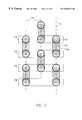
- FIG. 3shows a top-down example of a portion of a preferred embodiment memory array of SOI Vertical Array Device Trench Capacitor DRAM of FIG. 2 J.
- the bitline (BL) diffusions 164are shared by cell pairs at opposite sides of the SOI islands and are connected to bit line contacts 174 represented by X's.
- Bitlines 176are represented by vertical dashed lines and wordlines 178 are spaced horizontally. Accordingly, the preferred embodiment cells form an array of a densely packed DRAM cell for high density, high capacity high performance DRAM chips.
- bitline contact 174 and bitline diffusion regions 164being shared by two adjacent cell structures as shown in FIG. 2 J.
- bitline contacts structures 174 , 164may also be formed without departing in spirit or scope from the present invention.
Landscapes
- Engineering & Computer Science (AREA)
- Manufacturing & Machinery (AREA)
- Semiconductor Memories (AREA)
Abstract
Description
1. Field of the Invention
The present invention generally relates to semiconductor memories and, more particularly, to a trench capacitor dynamic random access memory cell with a vertical silicon on insulator access transistor for semiconductor memories.
2. Background Description
Dynamic Random Access Memory (DRAM) cells are well known. A DRAM cell is essentially a capacitor for storing charge and a pass transistor (also called a pass gate or access transistor) for transferring charge to and from the capacitor. Data (1 bit) stored in the cell is determined by the absence or presence of charge on the storage capacitor. Because cell size determines chip density, size and cost, reducing cell area is one of the DRAM designer's primary goals. Reducing cell area is done, normally, by reducing feature size to shrink the cell.
Besides shrinking the cell features, the most effective way to reduce cell area is to reduce the largest feature in the cell, typically, the area of the storage capacitor. Unfortunately, shrinking the capacitor plate area reduces capacitance and, consequently, reduces stored charge. Reduced charge means that what charge is stored in the DRAM is more susceptible to noise, soft errors, leakage and other well known DRAM problems. Consequently, another primary goal for DRAM cell designers is to maintain storage capacitance while reducing cell area.
One way to accomplish this density goal without sacrificing storage capacitance is to use trench capacitors in the cells. Typically, trench capacitors are formed by etching long deep trenches in a silicon wafer and, then, placing each capacitor on its side in the trench, orienting the capacitors vertically with respect to the chip's surface. Thus, the surface area required for the storage capacitor is dramatically reduced without sacrificing capacitance, and correspondingly, storable charge.
However, since using a trench capacitor eliminates much of the cell surface area, i.e., that portion of cell area which was formerly required for the storage capacitor, the cell's access transistor has become the dominant cell feature determining array area. As a result, to further reduce cell and array area, efforts have been made to reduce access transistor area, which include making a vertical access transistor in the capacitor trench. See, for example, U.S. Pat. No. 5,006,909 entitled “DRAM With A Vertical Capacitor And Transistor” to Kosa.
Other approaches to using a vertical access transistor include U.S. Pat. No. 4,673,962 entitled “Vertical DRAM Cell and Method” to Chatterjee et al. and U.S. Pat. No. 5,102,817 entitled “Vertical DRAM Cell and Method” to Chatterjee et al. which both teach a vertical DRAM cell with a polysilicon channel access transistor. The polysilicon channel access transistor is formed in the same vertical polysilicon layer that serves as the cell storage capacitor plate.
U.S. Pat. No. 5,164,917 entitled “Vertical One-transistor DRAM With Enhanced Capacitance And Process for Fabricating” to Shichijo, U.S. Pat. No. 5,208,657 entitled “DRAM Cell With Trench Capacitor And Vertical Channel in Substrate” to Chatterjee et al., U.S. Pat. No. 5,225,697 entitled “Vertical DRAM Cell and Method” to Malhi et al. and U.S. Pat. No. 5,252,845 entitled “Trench DRAM Cell With Vertical Transistor” to Kim et al. all teach memory cells formed in small square deep trenches that have vertical access transistors. Further, the access transistor is annular, essentially, and formed on the trench sidewalls above the cell trench capacitor. Both Kim et al. and Shichijo teach DRAM cells wherein a layered storage capacitor is formed in and entirely enclosed in the trench.
For another approach, U.S. Pat. No. 5,103,276 entitled “High Performance Composed Pillar DRAM Cell” to Shen et al., U.S. Pat. No. 5,300,450 entitled “High Performance Composed Pillar DRAM Cell” to Shen et al. and U.S. Pat. No. 5,334,548 entitled “High Performance Composed Pillar DRAM Cell” to Shen et al. teach etching a grid-like pattern to form individual pillars. A common capacitor plate is formed at the bottom of the pillars. A diffusion on all sides of the bottom of the cell pillar serves as a cell storage node. Each pillar's storage diffusion is isolated from adjacent pillars by a dielectric pocket formed beneath the common capacitor plate. An access transistor channel is along one side of each pillar and disposed between the storage node and a bitline diffusion, which is at the top of the pillar. The access transistor gate is formed on one side of the pillar, above the common capacitor plate.
U.S. Pat. No. 5,281,837 entitled “Semiconductor Memory Device Having Cross-Point DRAM Cell Structure” to Kohyama, U.S. Pat. No. 5,362,665 entitled “Method of Making Vertical DRAM Cross-Point Memory Cell” to Lu and U.S. Pat. No. 5,710,056 entitled “DRAM With a Vertical Channel Structure And Process For Manufacturing The Same” to Hsu teach yet another approach wherein DRAM cells have their storage capacitor formed above the access transistor. U.S. Pat. No. 5,504,357 entitled “Dynamic Random Access Memory having A Vertical Transistor” to Kim et al. teaches a buried bitline transistor with the bitline formed at the bottom of a trench and the storage capacitor is formed above the transistor, at the wafer surface.
Performance is equally as important as density to DRAM design. Silicon-on-insulator (SOI) has be used to decrease parasitic capacitance and hence to improve integrated circuit chip performance. SOI reduces parasitic capacitance within the integrated circuit to reduce individual circuit loads, thereby improving circuit and chip performance. However, reducing parasitic capacitance is at odds with increasing or maintaining cell storage capacitance. Accordingly, SOI is seldom used for DRAM manufacture. One attempt at using SOI for DRAMS is taught in U.S. Pat. No. 5,888,864 entitled “Manufacturing Method of DRAM Cell Formed on An Insulating Layer Having a Vertical Channel” to Koh et al. Koh et al. teaches a SOI DRAM formed in a dual sided wafer circuit fabrication process. In the dual sided wafer fabrication process of Koh et al. storage capacitors are formed on one side of the wafer and, the access transistors are formed on the other side of the wafer.
Thus, there is a need for increasing the number of stored data bits per chip of Dynamic Random Access Memory (DRAM) products. There is also a need for improving DRAM electrical performance without impairing cell charge storage.
It is therefore a purpose of the present invention to increase the Dynamic Random Access Memory (DRAM) integration packing density;
It is another purpose of the present invention to decrease DRAM cell area;
It is yet another purpose of the present invention to increase the number of bits per DRAM chip;
It is yet another purpose of the present invention to reduce parasitic capacitance within DRAM chips;
It is yet another purpose of the present invention to improve DRAM electrical performance;
It is yet another purpose of the invention to achieve trench capacitor DRAM cell density while benefitting from the reduced parasitic capacitance, leakage and improved performance of silicon on insulator technology.
The present invention is a vertical trench-capacitor Dynamic Random Access Memory (DRAM) cell and array in a Silicon-On-Insulator (SOI) substrate and an SOI DRAM chip. The cell has a vertical trench capacitor and an insulated gate Field Effect Transistor (FET) formed on the trench sidewall. A buried oxide layer (BOX) in the SOI substrate forms a protective sidewall collar along the upper edge of the capacitor region. The vertical FET is formed along the upper sidewall of the trench, above the trench capacitor. A polysilicon strap formed along the sidewall at the BOX layer forms a self-aligned contact between the trench capacitor and the vertical FET. Thus, the cell occupies less horizontal chip area than a conventional planar DRAM cell.
The cells are formed in a silicon wafer by first forming the buried oxide layer in the wafer. Deep trenches are etched, initially, through the SOI layer and the BOX layer and protective sidewalls are formed. Then, the deep trenches are etched into the substrate. The trench volume in the substrate is expanded to form a bottle shaped trench. A polysilicon capacitor plate is formed in the deep trenches. Conductive polysilicon straps are formed in the trenches between the capacitor plates and the SOI layer sidewalls. Device regions are defined and a sidewall transistor gate is formed in the deep trenches. Shallow trenches isolation (STI) is used to isolate and define cells. Bitlines and wordlines are formed.
The foregoing and other objects, aspects and advantages will be better understood from the following detailed preferred embodiment description with reference to the drawings, in which:
FIG. 1 is a flow diagram of the preferred embodiment process for forming a vertical DRAM cell;
FIGS. 2A-J illustrate the steps of the process of forming vertical DRAM cells according to FIG. 1;
FIG. 3 shows a top-down example of a portion of a preferred embodiment memory array of SOI Vertical Array Device Trench Capacitor DRAM of FIG.2J.
Referring now to the drawings, and more particularly, FIG. 1 shows a flow diagram of the preferred embodiment silicon-on-insulator (SOI) process for forming vertical DRAM cells. First, if a SOI wafer has not been previously prepared, then, instep 100, the SOI wafer is prepared from a semiconductor wafer. Preferably, the initial wafer is a single crystal silicon wafer. A buried oxide (BOX) layer is formed in the silicon wafer. The BOX layer isolates a silicon layer (SOI layer) above the BOX layer from a thick substrate below the BOX layer, which is much thicker than the silicon layer. Then, in step102 a deep trench location pattern is formed, preferably, using a typical photolithographic process. Deep trenches are partially etched into the wafer, etching through the silicon layer and the BOX layer down to the thicker substrate. A protective spacer is formed along the sidewalls of the partially etched trenches to protect the SOI layer sidewalls. Instep 104 the deep trenches are completed, etching into the thick substrate to the full trench depth. Then, instep 106, the trench volume is expanded below the BOX layer to form bottle shaped trenches.
The trench capacitor formation begins instep 108 by forming a buried capacitor plate in the expanded portion of the bottle shaped trench. Then, instep 110, the upper portion of the protective sidewall spacers are removed, along the SOI layer, and the spacers are recessed (but not removed) below the upper surface of the buried plate. In step112 a conformal strap layer is formed filling the recesses. The strap layer forms a conductive strap between the capacitor plate and the silicon layer sidewall. Instep 114 the straps are defined when excess strap material is removed, preferably using an appropriate well known photolithographic process. Instep 115 oxide is formed on top of the capacitor plate, i.e., trench top oxide (TTO). Instep 116 the wafer is implanted to define n-wells, p-wells and a buried n-type region (n-band) that couples the storage capacitors' reference plates (i.e., the substrate sidewall) in common. A gate oxide is grown on the sidewalls. The trenches are filled with gate conductor material, instep 118 and shallow trenches are formed which define isolated silicon islands of the SOI layer. Also, the shallow trenches isolate cells on the islands from cells on adjacent islands. Wordline and bitline formation complete cell formation.
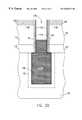
FIGS. 2A-J illustrate the steps of the process of forming a vertical DPAM cell in adeep trench 120 in an SOI wafer according to the steps of FIG.1. As noted above, theBOX layer 122 is formed in a single crystal silicon wafer. TheBOX layer 122 separates the surfaceSOI silicon layer 124 from the remainingthicker silicon substrate 126. Preferably, theBOX layer 122 is formed using a high-dose oxygen ion implantation in the single crystal wafer. However, any other suitable SOI technique may be employed. Thepreferred BOX layer 122 thickness is 300 nm, but theBOX layer 122 may be 10 nm to 500 nm thick. Further,BOX layer 122 thickness may be selected by adjusting ion implantation dose and energy. TheSOI surface layer 124, preferably, is 500 nm thick. However, depending on the desired cell access transistor channel length, theSOI layer 124 may be 100 nm to 1000 nm thick. TheSOI layer 124 thickness may be adjusted using a combination of chemical vapor deposition (CVD) epitaxial growth and/or etching and polishing. Having thus prepared the layered SOI wafer, memory cells may be formed according to the present invention.
Apad layer 128 of an insulating material such as silicon nitride (SiN) is formed on theupper surface 130 ofsilicon layer 124. Thepad layer 128 may be formed using, for example, low-pressure CVD (LPCVD) depositing SiN to a thickness of 10 nm to 500 nm, preferably 200 nm. Optionally, prior to forming the padLPCVD SiN layer 128, a thin (2 nm to 10 nm, preferably 5 nm) thermal oxide layer (not shown) may be formed on theSOI silicon layer 124.
In FIG. 2B, thedeep trenches 120 are completed, etchinglower area 140 intosubstrate 126 instep 104. Preferably RIE is used to etch thetrenches 120 to their full depth of 3 μm to 10 μm, preferably 6 μm. Then, thehard mask 132 is removed, preferably, using a hydrofluoric acid solution. As intended, thesidewall spacers 134 protect thesilicon layer 126trench sidewalls BOX layer 122 trench sidewalls.
In FIG. 2C thelower region 140 of thetrench 120 is enlarged to form a trench with a bottle shaped cross section instep 106. A suitable wet or dry etch process is used to etch away exposed substrate silicon from the sidewalls in thelower region 140. Again, theSOI layer 124 remains protected by thesidewall spacers 134,BOX 122 andpad film 128. The extent of substrate silicon removed in thislower trench area 140 is limited laterally by the selected array cell spacing and, preferably, is such that the trench is expanded in thislower area 140 by less than 30% of the distance to the nearest neighboring trench. Thus, the substrate thickness between neighboring trench sidewalls in thislower area 140 is >70% of thetrench 120 separation at the surface. Optionally, at this point, the exposed substrate in thelower trench area 140 may be doped to form acommon capacitor plate 142. If doped, thelower trench area 140 is doped with an n-type dopant to a concentration of 1018-1019using a gas-phase doping or other suitable doping techniques.
It should be noted that the preferred embodiment described herein is described with device regions being doped for a particular device type, i.e., n-type FET (NFET). The selected device type described herein is for example only and not intended as a limitation. A person of ordinary skill would understand how to replace NFETs with p-type FETs (PFETs) and n-type dopant with p-type dopant where appropriate without departing from the spirit or scope of the invention.
Returning to the drawings, in FIG. 2D individual cell storage capacitor plates are formed in the expandedlower region 140 instep 108. First, athin capacitor dielectric 144 is formed ontrench 120 surfaces, preferably using LPCVD SiN. The thinSiN dielectric layer 144 is preferably 3.5 nm thick and may be from 2-10 nm thick. Then, a conductive material, preferably doped polysilicon, is deposited of sufficient thickness to fill thetrench 120 using LPCVD. The wafer is planarized to remove surface polysilicon. The plate is completed by recessing the polysilicon to a point just above theBOX layer 122, preferably, using a SF6plasma dry etch.
In FIG. 2E the thinSiN dielectric layer 144 is stripped and thesidewall spacer 134 is removed along the SOI layer and sub-etched beneath thepolysilicon plate 146 instep 110 to formrecesses 148 around the upper surface ofplate 146.Protective spacers 134′ remain along theBOX layer 122 sidewalls. Preferably, the sidewall spacer material is subetched using a wet etch such as a hydrofluoric acid solution.
Next, an interfacial treatment of a thin dielectric surface layer (not shown), such as a 1 nm oxide or nitride layer, is formed onSOT sidewalls recesses 148 along the exposed sides ofpolysilicon plate 146. Preferably, the interfacial treatment is a thin nitride layer between 0.5 nm and 2 nm, preferably 1 nm, formed with a thermal nitridation. This thin dielectric, interfacial treatment layer controls and limits the extent of outdiffusion from thepolysilicon plate 134 intoSOI layer 124. Therefore, the thin dielectric interfacial treatment layer is not completely isolating, but is electrically conductive for electron tunneling along the side ofpolysilicon plate 146 and at thesidewalls SOT layer 124.
Turning to FIG. 2F, astrap layer 150 is formed instep 112. Preferably, thestrap layer 150 is formed by depositing a conformal layer of heavily doped polysilicon using LPCVD. The polysilicon strap layer is 10 nm-50 nm thick, preferably 30 nm, and doped with n-type dopant. Further, the strap layer completely fills the recessedspacer region 148 aboveprotective spacers 134′.
Then, as shown by the cross section of FIG. 2G, straps152 are defined instep 114. Exposed horizontal and vertical areas ofstrap layer 150 are isotopically etched away to definestraps 152 which strap cell capacitor plates to access transistor source regions. Polysilicon straps152 are defined inrecess area 148 using a selective wet or dry etch, selective to nitride, to remove the exposedstrap layer 148 along thesidewalls pad nitride 128. Eachpolysilicon strap 152 is a self-aligned buried strap that makes an electrical connection between thepolysilicon plate 146 and thetrench sidewalls SOI layer 124 and, essentially, completes cell storage capacitor definition.
In FIG. 2H a trench-top-oxide (TTO)pad 154 is formed above the strappedpolysilicon plug 146.TTO pad 154 isolates the cell storage capacitor from the cell transfer gate FET formed thereabove instep 115. So, theTTO pad 146 is formed by anisotropically depositing an oxide layer on the horizontal surfaces of the wafer, which includes the top156 ofpolysilicon plates 146. Then, using a suitable chemical mechanical polishing (CMP) process, the oxide layer is removed from thepad SiN layer 128 but, remains in thetrenches 120 on polysilicon plugs146. Then, thepad nitride layer 128 is stripped away using conventional wet etch. A sacrificial thermal oxide layer is grown on the wafer to a thickness of 5 nm to 20 nm, preferably 10 nm. Primarily, the sacrificial oxide layer is formed to heal any damage to theSOI layer 124sidewalls surface 130 of theSOI layer 124 that may have occurred during the previous steps.
Next instep 116, as shown in FIG. 2I, device regions are defined.Device wells 158, p-wells, are defined by implanting a p-type dopant, in this example, into the wafer. The commoncapacitor plate diffusions 142 in adjacent array cells are connected together by a layer of an n-type dopant implanted intosubstrate 126 to form an n-band layer 160. Then, the sacrificial surface oxide is stripped using a HF solution, andgate oxide 162 is grown alongsurface 130 and onsidewalls gate oxide 162 is 2 nm to 20 nm, preferably 5 nm.
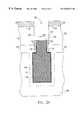
Then, adrain diffusion layer 164 in FIG. 2J, preferably n-type, is implanted and diffused into the upper issurface 130 of theSOI layer 124. During subsequent thermal processing and coincidentally with diffusing thedrain diffusion layer 164, dopant outdiffuses from remainingstraps 152 forming self-alignedsource diffusion 166. The diffusion that forms from this outdiffusion connects the source of the cell transfer device to the cellstorage capacitor plate 146.
Then, the cell's access transistor gate is formed, cells are isolated and word and bit lines are defined and formed instep 118. A layer of conductive material is deposited of sufficient thickness to fill thetrenches 120, preferably, using LPCVD to deposit doped polysilicon. A protective nitride pad layer (not shown) is deposited on the polysilicon layer. Then,device isolation trenches 168 are formed using a conventional shallow trench isolation (STI) process, such as photolithography and a dry etch, e.g, RIE. The RIE-formedshallow trenches 168 remove onedeep trench sidewall 138 and extend down through theSOI silicon layer 124 and partially through theBOX layer 122 and at least to the top of theprotective spacer 134′. Thus, theshallow trenches 168, essentially form isolated silicon islands of theSOI layer 124 onBOX layer 122 with apolysilicon gate 170 along the remainingdeep trench sidewall 136, thereby forming the cell's access transistor gate. Theshallow trenches 168 are filled with insulating material such as silicon dioxide using, preferably, an anisotropic high density plasma (HDP) deposition.
Then, excess silicon dioxide is removed and the wafer surface is planarized to the protective pad SiN surface using a conventional CMP process. The protective pad SiN is stripped from the wafer using a standard wet etch. A wordline layer, preferably a polysilicon layer, is formed on the surface. The wordline layer is patterned to form wordlines (WL)172 in contact with theaccess transistor gates 170 using a well known word line definition technique. Abitline contact 174 is formed at thedrain diffusion layer 164 using conventional a bitline formation technique.
FIG. 3 shows a top-down example of a portion of a preferred embodiment memory array of SOI Vertical Array Device Trench Capacitor DRAM of FIG.2J. The bitline (BL) diffusions164 are shared by cell pairs at opposite sides of the SOI islands and are connected to bitline contacts 174 represented by X's.Bitlines 176 are represented by vertical dashed lines andwordlines 178 are spaced horizontally. Accordingly, the preferred embodiment cells form an array of a densely packed DRAM cell for high density, high capacity high performance DRAM chips.
It should be noted that the preferred embodiment as described herein withbitline contact 174 andbitline diffusion regions 164 being shared by two adjacent cell structures as shown in FIG.2J. Those skilled in the art will recognize that other cell layouts, such as those that do not sharebitline contacts structures
While the invention has been described in terms of preferred embodiments, those skilled in the art will recognize that the invention can be practiced with modification within the spirit and scope of the appended claims.
Claims (9)
1. A method of forming a memory cell in a layered semiconductor wafer, said layered semiconductor wafer comprising the steps of:
a) forming a buried oxide (BOX) layer in said layered semiconductor wafer;
b) etching through said BOX layer to form a trench capacitor;
c) forming a conductive strap from a plate of said trench capacitor to a trench sidewall of a top layer of said layered semiconductor wafer;
d) forming a vertical transistor along said trench sidewall of said semiconductor layer; and
e) forming semiconductor islands of said top semiconductor layer, said vertical transistor being one of said semiconductor islands.
2. The method ofclaim 1 , wherein said semiconductor wafer is a silicon wafer, said BOX layer isolating the top silicon layer from a thicker silicon substrate beneath said BOX layer, and the step b) of forming a trench capacitor comprises forming a bottle shaped trench in said layered wafer, said trench capacitor being formed in said bottle shaped trench.
3. The method ofclaim 2 , wherein forming the bottle shaped trench comprises the steps of:
i) etching an upper portion of a first trench through said silicon layer and said BOX layer;
ii) forming protective sidewall layer in said upper portion of said first trench; and
iii) etching said first trench into the thicker silicon substrate.
4. The method ofclaim 3 , wherein forming the bottle shaped trench further comprises:
iv) expanding said trenches in said thicker silicon substrate; and
v) forming a polysilicon plate in said bottle shaped trench.
5. The method ofclaim 4 , wherein the step (c) of forming the conductive strap comprises:
i) partially removing said protective sidewall layers to a point below a top of said polysilicon plate, recesses being formed between said polysilicon plate and sidewalls of said bottle shaped trench;
ii) forming a conductive strap layer in said trenches, said conductive strap layer filling said recesses; and
iii) selectively removing said conductive strap layer from said trenches, conductive straps remaining in said recesses.
6. The method ofclaim 5 , wherein the step (d) of forming the vertical transistor comprises the steps of:
i) forming an oxide layer on the polysilicon plate and said conductive strap;
ii) forming a gate oxide layer on sidewalls of said top silicon layer;
iii) filling said trench with gate material; and
iv) forming a conductive region at an upper surface of said top silicon layer.
7. The method ofclaim 6 , wherein the conductive region is a drain diffusion region and wherein when said drain diffusion region is formed dopant outdiffuses from said conductive strap into a lower portion of said top silicon layer forming a source diffusion region.
8. The method ofclaim 7 , wherein the step (e) of forming the silicon islands comprises the steps of:
i) forming a plurality of isolation trenches through said top silicon layer and partially through said BOX layer; and
ii) filling said isolation trenches with insulating material.
9. A method of forming a memory array of memory cells as inclaim 8 , said further comprising the steps of:
e) forming wordlines connected to a plurality of said vertical transistor gates; and
f) forming a plurality of bitlines connected to a plurality of vertical transistor drain diffusions.
Priority Applications (1)
| Application Number | Priority Date | Filing Date | Title |
|---|---|---|---|
| US09/427,257US6566177B1 (en) | 1999-10-25 | 1999-10-25 | Silicon-on-insulator vertical array device trench capacitor DRAM |
Applications Claiming Priority (1)
| Application Number | Priority Date | Filing Date | Title |
|---|---|---|---|
| US09/427,257US6566177B1 (en) | 1999-10-25 | 1999-10-25 | Silicon-on-insulator vertical array device trench capacitor DRAM |
Publications (1)
| Publication Number | Publication Date |
|---|---|
| US6566177B1true US6566177B1 (en) | 2003-05-20 |
Family
ID=23694123
Family Applications (1)
| Application Number | Title | Priority Date | Filing Date |
|---|---|---|---|
| US09/427,257Expired - LifetimeUS6566177B1 (en) | 1999-10-25 | 1999-10-25 | Silicon-on-insulator vertical array device trench capacitor DRAM |
Country Status (1)
| Country | Link |
|---|---|
| US (1) | US6566177B1 (en) |
Cited By (102)
| Publication number | Priority date | Publication date | Assignee | Title |
|---|---|---|---|---|
| US20030071616A1 (en)* | 2001-09-08 | 2003-04-17 | Henning Hauenstein | Device for measuring the strength of a vector component of a magnetic field, current-measuring device and use of a field-effect transistor |
| US20030073271A1 (en)* | 2001-10-12 | 2003-04-17 | Albert Birner | Method of forming a vertical field-effect transistor device |
| US20030132504A1 (en)* | 2000-05-31 | 2003-07-17 | International Business Machines Corporation | Structures and methods of anti-fuse formation in SOI |
| US6696717B2 (en)* | 2002-07-09 | 2004-02-24 | Nanya Technology Corporation | Memory cell with vertical transistor and trench capacitor |
| US20040124488A1 (en)* | 2001-06-18 | 2004-07-01 | Pierre Fazan | Semiconductor device |
| US20040157389A1 (en)* | 2001-03-09 | 2004-08-12 | Wolfgang Gustin | Semiconductor memory cell and method for fabricating the memory cell |
| US6787838B1 (en)* | 2003-06-18 | 2004-09-07 | International Business Machines Corporation | Trench capacitor DRAM cell using buried oxide as array top oxide |
| US20040227166A1 (en)* | 2003-05-13 | 2004-11-18 | Lionel Portmann | Reference current generator, and method of programming, adjusting and/or operating same |
| US20040228168A1 (en)* | 2003-05-13 | 2004-11-18 | Richard Ferrant | Semiconductor memory device and method of operating same |
| US20040238890A1 (en)* | 2002-04-18 | 2004-12-02 | Pierre Fazan | Semiconductor device |
| US20040240306A1 (en)* | 2002-04-18 | 2004-12-02 | Pierre Fazan | Data storage device and refreshing method for use with such device |
| US20050013163A1 (en)* | 2003-05-13 | 2005-01-20 | Richard Ferrant | Semiconductor memory cell, array, architecture and device, and method of operating same |
| US20050017240A1 (en)* | 2003-07-22 | 2005-01-27 | Pierre Fazan | Integrated circuit device, and method of fabricating same |
| US20050063224A1 (en)* | 2003-09-24 | 2005-03-24 | Pierre Fazan | Low power programming technique for a floating body memory transistor, memory cell, and memory array |
| US20050285175A1 (en)* | 2004-06-23 | 2005-12-29 | International Business Machines Corporation | Vertical SOI Device |
| US20060091462A1 (en)* | 2004-11-04 | 2006-05-04 | Serguei Okhonin | Memory cell having an electrically floating body transistor and programming technique therefor |
| US20060098481A1 (en)* | 2004-11-10 | 2006-05-11 | Serguei Okhonin | Circuitry for and method of improving statistical distribution of integrated circuits |
| US20060124936A1 (en)* | 2004-12-09 | 2006-06-15 | International Business Machines Corporation | Soi device with different crystallographic orientations |
| US20060126374A1 (en)* | 2004-12-13 | 2006-06-15 | Waller William K | Sense amplifier circuitry and architecture to write data into and/or read from memory cells |
| US20060131650A1 (en)* | 2004-12-22 | 2006-06-22 | Serguei Okhonin | Bipolar reading technique for a memory cell having an electrically floating body transistor |
| US20060163636A1 (en)* | 2005-01-21 | 2006-07-27 | International Business Machines Corporation | Trench capacitor array having well contacting merged plate |
| US20060175660A1 (en)* | 2005-02-10 | 2006-08-10 | International Business Machines Corporation | Vertical body-contacted soi transistor |
| US20070023833A1 (en)* | 2005-07-28 | 2007-02-01 | Serguei Okhonin | Method for reading a memory cell having an electrically floating body transistor, and memory cell and array implementing same |
| US20070045697A1 (en)* | 2005-08-31 | 2007-03-01 | International Business Machines Corporation | Body-contacted semiconductor structures and methods of fabricating such body-contacted semiconductor structures |
| US20070045698A1 (en)* | 2005-08-31 | 2007-03-01 | International Business Machines Corporation | Semiconductor structures with body contacts and fabrication methods thereof |
| US20070058427A1 (en)* | 2005-09-07 | 2007-03-15 | Serguei Okhonin | Memory cell and memory cell array having an electrically floating body transistor, and methods of operating same |
| US20070064489A1 (en)* | 2005-09-19 | 2007-03-22 | Philippe Bauser | Method and circuitry to generate a reference current for reading a memory cell, and device implementing same |
| US20070085140A1 (en)* | 2005-10-19 | 2007-04-19 | Cedric Bassin | One transistor memory cell having strained electrically floating body region, and method of operating same |
| US20070138530A1 (en)* | 2005-12-19 | 2007-06-21 | Serguei Okhonin | Electrically floating body memory cell and array, and method of operating or controlling same |
| US20070176237A1 (en)* | 2002-05-13 | 2007-08-02 | Kabushiki Kaisha Toshiba | Semiconductor device and manufacturing method thereof |
| US20070187775A1 (en)* | 2006-02-16 | 2007-08-16 | Serguei Okhonin | Multi-bit memory cell having electrically floating body transistor, and method of programming and reading same |
| US20070235801A1 (en)* | 2006-04-04 | 2007-10-11 | International Business Machines Corporation | Self-aligned body contact for a semicondcutor-on-insulator trench device and method of fabricating same |
| US20070285982A1 (en)* | 2006-04-07 | 2007-12-13 | Eric Carman | Memory array having a programmable word length, and method of operating same |
| US20070284612A1 (en)* | 2006-06-09 | 2007-12-13 | International Business Machines Corporation | Semiconductor devices with one-sided buried straps |
| US20080013359A1 (en)* | 2006-07-11 | 2008-01-17 | David Fisch | Integrated circuit including memory array having a segmented bit line architecture and method of controlling and/or operating same |
| US20080230822A1 (en)* | 2007-03-20 | 2008-09-25 | International Business Machines Corporation | Vertical trench memory cell with insulating ring |
| US20080242096A1 (en)* | 2007-03-30 | 2008-10-02 | Promos Technologies Inc. | Method for preparing bottle-shaped deep trenches |
| US20080258268A1 (en)* | 2007-04-18 | 2008-10-23 | International Business Machines Corporation | Trench structure and method of forming the trench structure |
| US20080308855A1 (en)* | 2007-06-12 | 2008-12-18 | Micron Technology, Inc. | Memory devices with isolation structures and methods of forming and programming the same |
| US20090016101A1 (en)* | 2007-06-01 | 2009-01-15 | Serguei Okhonin | Reading Technique for Memory Cell With Electrically Floating Body Transistor |
| US20090032855A1 (en)* | 2007-07-31 | 2009-02-05 | Patrick Press | Method for forming a deep trench in an soi device by reducing the shielding effect of the active layer during the deep trench etch process |
| US20090108306A1 (en)* | 2007-10-31 | 2009-04-30 | International Business Machines Corporation | Uniform recess of a material in a trench independent of incoming topography |
| US20090176347A1 (en)* | 2008-01-04 | 2009-07-09 | International Business Machines Corporation | Hybrid orientation substrate compatible deep trench capacitor embedded dram |
| US20090201723A1 (en)* | 2008-02-06 | 2009-08-13 | Serguei Okhonin | Single Transistor Memory Cell |
| US20090230471A1 (en)* | 2008-03-14 | 2009-09-17 | International Business Machines Corporation | Trench memory with self-aligned strap formed by self-limiting process |
| US20090230508A1 (en)* | 2008-03-14 | 2009-09-17 | International Business Machines Corporation | Soi protection for buried plate implant and dt bottle etch |
| US7606098B2 (en) | 2006-04-18 | 2009-10-20 | Innovative Silicon Isi Sa | Semiconductor memory array architecture with grouped memory cells, and method of controlling same |
| US20090289291A1 (en)* | 2008-05-21 | 2009-11-26 | International Business Machines Corporation | Soi deep trench capacitor employing a non-conformal inner spacer |
| US20100038745A1 (en)* | 2008-08-18 | 2010-02-18 | Promos Technologies Inc. | Integrated circuit structure having bottle-shaped isolation |
| US20100142294A1 (en)* | 2008-12-05 | 2010-06-10 | Eric Carman | Vertical Transistor Memory Cell and Array |
| US20100144106A1 (en)* | 2008-12-08 | 2010-06-10 | Advanced Micro Devices, Inc. | Dynamic random access memory (dram) cells and methods for fabricating the same |
| US20100258904A1 (en)* | 2009-04-14 | 2010-10-14 | International Business Machines Corporation | Bottle-shaped trench capacitor with enhanced capacitance |
| US20100296327A1 (en)* | 2009-05-22 | 2010-11-25 | Innovative Silicon Isi Sa | Techniques for providing a direct injection semiconductor memory device |
| US7924630B2 (en) | 2008-10-15 | 2011-04-12 | Micron Technology, Inc. | Techniques for simultaneously driving a plurality of source lines |
| US20110084332A1 (en)* | 2009-10-08 | 2011-04-14 | Vishay General Semiconductor, Llc. | Trench termination structure |
| US7933142B2 (en) | 2006-05-02 | 2011-04-26 | Micron Technology, Inc. | Semiconductor memory cell and array using punch-through to program and read same |
| US7933140B2 (en) | 2008-10-02 | 2011-04-26 | Micron Technology, Inc. | Techniques for reducing a voltage swing |
| US7947543B2 (en) | 2008-09-25 | 2011-05-24 | Micron Technology, Inc. | Recessed gate silicon-on-insulator floating body device with self-aligned lateral isolation |
| US20110122687A1 (en)* | 2009-11-24 | 2011-05-26 | Innovative Silicon Isi Sa | Techniques for reducing disturbance in a semiconductor device |
| US7957206B2 (en) | 2008-04-04 | 2011-06-07 | Micron Technology, Inc. | Read circuitry for an integrated circuit having memory cells and/or a memory cell array, and method of operating same |
| US20110199848A1 (en)* | 2010-02-12 | 2011-08-18 | Innovative Silicon Isi Sa | Techniques for controlling a semiconductor memory device |
| US8008160B2 (en) | 2008-01-21 | 2011-08-30 | International Business Machines Corporation | Method and structure for forming trench DRAM with asymmetric strap |
| US8064274B2 (en) | 2007-05-30 | 2011-11-22 | Micron Technology, Inc. | Integrated circuit having voltage generation circuitry for memory cell array, and method of operating and/or controlling same |
| US8069377B2 (en) | 2006-06-26 | 2011-11-29 | Micron Technology, Inc. | Integrated circuit having memory array including ECC and column redundancy and method of operating the same |
| US20110316061A1 (en)* | 2010-06-24 | 2011-12-29 | International Business Machines Corporation | Structure and method to control bottom corner threshold in an soi device |
| US8139418B2 (en) | 2009-04-27 | 2012-03-20 | Micron Technology, Inc. | Techniques for controlling a direct injection semiconductor memory device |
| US8189376B2 (en) | 2008-02-08 | 2012-05-29 | Micron Technology, Inc. | Integrated circuit having memory cells including gate material having high work function, and method of manufacturing same |
| US8194487B2 (en) | 2007-09-17 | 2012-06-05 | Micron Technology, Inc. | Refreshing data of memory cells with electrically floating body transistors |
| US8199595B2 (en) | 2009-09-04 | 2012-06-12 | Micron Technology, Inc. | Techniques for sensing a semiconductor memory device |
| US8223574B2 (en) | 2008-11-05 | 2012-07-17 | Micron Technology, Inc. | Techniques for block refreshing a semiconductor memory device |
| US8227311B2 (en) | 2010-10-07 | 2012-07-24 | International Business Machines Corporation | Method of forming enhanced capacitance trench capacitor |
| US8241981B1 (en) | 2011-01-31 | 2012-08-14 | International Business Machines Corporation | Method of fabricating a deep trench (DT) metal-insulator-metal (MIM) capacitor |
| US8264041B2 (en) | 2007-01-26 | 2012-09-11 | Micron Technology, Inc. | Semiconductor device with electrically floating body |
| WO2012099838A3 (en)* | 2011-01-19 | 2012-10-26 | International Business Machines Corporation | Structure and method for hard mask removal on an soi substrate without using cmp process |
| US8310893B2 (en) | 2009-12-16 | 2012-11-13 | Micron Technology, Inc. | Techniques for reducing impact of array disturbs in a semiconductor memory device |
| US8315099B2 (en) | 2009-07-27 | 2012-11-20 | Micron Technology, Inc. | Techniques for providing a direct injection semiconductor memory device |
| US8319294B2 (en) | 2009-02-18 | 2012-11-27 | Micron Technology, Inc. | Techniques for providing a source line plane |
| US20120305998A1 (en)* | 2011-05-31 | 2012-12-06 | International Business Machines Corporation | High density memory cells using lateral epitaxy |
| US8349662B2 (en) | 2007-12-11 | 2013-01-08 | Micron Technology, Inc. | Integrated circuit having memory cell array, and method of manufacturing same |
| US8369177B2 (en) | 2010-03-05 | 2013-02-05 | Micron Technology, Inc. | Techniques for reading from and/or writing to a semiconductor memory device |
| US8411513B2 (en) | 2010-03-04 | 2013-04-02 | Micron Technology, Inc. | Techniques for providing a semiconductor memory device having hierarchical bit lines |
| US8411524B2 (en) | 2010-05-06 | 2013-04-02 | Micron Technology, Inc. | Techniques for refreshing a semiconductor memory device |
| US20130102123A1 (en)* | 2011-10-19 | 2013-04-25 | Nanya Technology Corporation | Method for fabricating single-sided buried strap in a semiconductor device |
| US8455875B2 (en) | 2010-05-10 | 2013-06-04 | International Business Machines Corporation | Embedded DRAM for extremely thin semiconductor-on-insulator |
| US8508994B2 (en) | 2009-04-30 | 2013-08-13 | Micron Technology, Inc. | Semiconductor device with floating gate and electrically floating body |
| US8518774B2 (en) | 2007-03-29 | 2013-08-27 | Micron Technology, Inc. | Manufacturing process for zero-capacitor random access memory circuits |
| US8531878B2 (en) | 2011-05-17 | 2013-09-10 | Micron Technology, Inc. | Techniques for providing a semiconductor memory device |
| US8536628B2 (en) | 2007-11-29 | 2013-09-17 | Micron Technology, Inc. | Integrated circuit having memory cell array including barriers, and method of manufacturing same |
| US8537610B2 (en) | 2009-07-10 | 2013-09-17 | Micron Technology, Inc. | Techniques for providing a semiconductor memory device |
| US8547738B2 (en) | 2010-03-15 | 2013-10-01 | Micron Technology, Inc. | Techniques for providing a semiconductor memory device |
| US8576631B2 (en) | 2010-03-04 | 2013-11-05 | Micron Technology, Inc. | Techniques for sensing a semiconductor memory device |
| US8637365B2 (en) | 2012-06-06 | 2014-01-28 | International Business Machines Corporation | Spacer isolation in deep trench |
| US8710566B2 (en) | 2009-03-04 | 2014-04-29 | Micron Technology, Inc. | Techniques for forming a contact to a buried diffusion layer in a semiconductor memory device |
| US8748959B2 (en) | 2009-03-31 | 2014-06-10 | Micron Technology, Inc. | Semiconductor memory device |
| US8773933B2 (en) | 2012-03-16 | 2014-07-08 | Micron Technology, Inc. | Techniques for accessing memory cells |
| US8907396B2 (en) | 2012-01-04 | 2014-12-09 | Micron Technology, Inc | Source/drain zones with a delectric plug over an isolation region between active regions and methods |
| US9105691B2 (en) | 2013-04-09 | 2015-08-11 | International Business Machines Corporation | Contact isolation scheme for thin buried oxide substrate devices |
| US9214378B2 (en)* | 2012-06-29 | 2015-12-15 | International Business Machines Corporation | Undercut insulating regions for silicon-on-insulator device |
| US9406683B2 (en)* | 2014-12-04 | 2016-08-02 | International Business Machines Corporation | Wet bottling process for small diameter deep trench capacitors |
| US9559216B2 (en) | 2011-06-06 | 2017-01-31 | Micron Technology, Inc. | Semiconductor memory device and method for biasing same |
| US20200135634A1 (en)* | 2018-10-26 | 2020-04-30 | Taiwan Semiconductor Manufacturing Company, Ltd. | Buried Power Rail and Method Forming Same |
| TWI767651B (en)* | 2020-05-07 | 2022-06-11 | 美商應用材料股份有限公司 | Structures and methods for forming dynamic random-access memory devices |
Citations (25)
| Publication number | Priority date | Publication date | Assignee | Title |
|---|---|---|---|---|
| US4673962A (en) | 1985-03-21 | 1987-06-16 | Texas Instruments Incorporated | Vertical DRAM cell and method |
| US5006909A (en) | 1989-10-30 | 1991-04-09 | Motorola, Inc. | Dram with a vertical capacitor and transistor |
| US5065273A (en)* | 1990-12-04 | 1991-11-12 | International Business Machines Corporation | High capacity DRAM trench capacitor and methods of fabricating same |
| US5102817A (en) | 1985-03-21 | 1992-04-07 | Texas Instruments Incorporated | Vertical DRAM cell and method |
| US5164917A (en) | 1985-06-26 | 1992-11-17 | Texas Instruments Incorporated | Vertical one-transistor DRAM with enhanced capacitance and process for fabricating |
| US5208657A (en) | 1984-08-31 | 1993-05-04 | Texas Instruments Incorporated | DRAM Cell with trench capacitor and vertical channel in substrate |
| US5225697A (en) | 1984-09-27 | 1993-07-06 | Texas Instruments, Incorporated | dRAM cell and method |
| US5252845A (en) | 1990-04-02 | 1993-10-12 | Electronics And Telecommunications Research Institute | Trench DRAM cell with vertical transistor |
| US5281837A (en) | 1990-05-28 | 1994-01-25 | Kabushiki Kaisha Toshiba | Semiconductor memory device having cross-point DRAM cell structure |
| US5300450A (en) | 1988-06-01 | 1994-04-05 | Texas Instruments Incorporated | High performance composed pillar DRAM cell |
| US5362665A (en) | 1994-02-14 | 1994-11-08 | Industrial Technology Research Institute | Method of making vertical DRAM cross point memory cell |
| US5369049A (en)* | 1993-12-17 | 1994-11-29 | International Business Machines Corporation | DRAM cell having raised source, drain and isolation |
| US5384277A (en)* | 1993-12-17 | 1995-01-24 | International Business Machines Corporation | Method for forming a DRAM trench cell capacitor having a strap connection |
| US5389559A (en)* | 1993-12-02 | 1995-02-14 | International Business Machines Corporation | Method of forming integrated interconnect for very high density DRAMs |
| US5422289A (en)* | 1992-04-27 | 1995-06-06 | National Semiconductor Corporation | Method of manufacturing a fully planarized MOSFET and resulting structure |
| US5504357A (en) | 1991-09-26 | 1996-04-02 | Hyundai Electronics Industries, Co., Ltd. | Dynamic random access memory having a vertical transistor |
| US5627092A (en)* | 1994-09-26 | 1997-05-06 | Siemens Aktiengesellschaft | Deep trench dram process on SOI for low leakage DRAM cell |
| US5710056A (en) | 1996-06-29 | 1998-01-20 | United Microelectronics Corporation | DRAM with a vertical channel structure and process for manufacturing the same |
| US5888864A (en) | 1996-10-22 | 1999-03-30 | Hyundai Electronics Industries Co., Ltd. | Manufacturing method of DRAM Cell formed on an insulating layer having a vertical channel |
| US5909044A (en)* | 1997-07-18 | 1999-06-01 | International Business Machines Corporation | Process for forming a high density semiconductor device |
| US6091094A (en)* | 1998-06-11 | 2000-07-18 | Siemens Aktiengesellschaft | Vertical device formed adjacent to a wordline sidewall and method for semiconductor chips |
| JP2000269494A (en)* | 1999-03-18 | 2000-09-29 | Toshiba Corp | Semiconductor element |
| US6180509B1 (en)* | 1995-07-28 | 2001-01-30 | Stmicroelectronics, Inc. | Method for forming planarized multilevel metallization in an integrated circuit |
| US6190971B1 (en)* | 1999-05-13 | 2001-02-20 | International Business Machines Corporation | Formation of 5F2 cell with partially vertical transistor and gate conductor aligned buried strap with raised shallow trench isolation region |
| US6211008B1 (en)* | 2000-03-17 | 2001-04-03 | Chartered Semiconductor Manufacturing, Ltd. | Method for forming high-density high-capacity capacitor |
- 1999
- 1999-10-25USUS09/427,257patent/US6566177B1/ennot_activeExpired - Lifetime
Patent Citations (28)
| Publication number | Priority date | Publication date | Assignee | Title |
|---|---|---|---|---|
| US5208657A (en) | 1984-08-31 | 1993-05-04 | Texas Instruments Incorporated | DRAM Cell with trench capacitor and vertical channel in substrate |
| US5225697A (en) | 1984-09-27 | 1993-07-06 | Texas Instruments, Incorporated | dRAM cell and method |
| US5102817A (en) | 1985-03-21 | 1992-04-07 | Texas Instruments Incorporated | Vertical DRAM cell and method |
| US4673962A (en) | 1985-03-21 | 1987-06-16 | Texas Instruments Incorporated | Vertical DRAM cell and method |
| US5164917A (en) | 1985-06-26 | 1992-11-17 | Texas Instruments Incorporated | Vertical one-transistor DRAM with enhanced capacitance and process for fabricating |
| US5300450A (en) | 1988-06-01 | 1994-04-05 | Texas Instruments Incorporated | High performance composed pillar DRAM cell |
| US5334548A (en) | 1988-06-01 | 1994-08-02 | Texas Instruments Incorporated | High performance composed pillar dRAM cell |
| US5006909A (en) | 1989-10-30 | 1991-04-09 | Motorola, Inc. | Dram with a vertical capacitor and transistor |
| US5252845A (en) | 1990-04-02 | 1993-10-12 | Electronics And Telecommunications Research Institute | Trench DRAM cell with vertical transistor |
| US5281837A (en) | 1990-05-28 | 1994-01-25 | Kabushiki Kaisha Toshiba | Semiconductor memory device having cross-point DRAM cell structure |
| US5065273A (en)* | 1990-12-04 | 1991-11-12 | International Business Machines Corporation | High capacity DRAM trench capacitor and methods of fabricating same |
| US5504357A (en) | 1991-09-26 | 1996-04-02 | Hyundai Electronics Industries, Co., Ltd. | Dynamic random access memory having a vertical transistor |
| US5422289A (en)* | 1992-04-27 | 1995-06-06 | National Semiconductor Corporation | Method of manufacturing a fully planarized MOSFET and resulting structure |
| US5389559A (en)* | 1993-12-02 | 1995-02-14 | International Business Machines Corporation | Method of forming integrated interconnect for very high density DRAMs |
| US5384277A (en)* | 1993-12-17 | 1995-01-24 | International Business Machines Corporation | Method for forming a DRAM trench cell capacitor having a strap connection |
| US5369049A (en)* | 1993-12-17 | 1994-11-29 | International Business Machines Corporation | DRAM cell having raised source, drain and isolation |
| US5362665A (en) | 1994-02-14 | 1994-11-08 | Industrial Technology Research Institute | Method of making vertical DRAM cross point memory cell |
| US5627092A (en)* | 1994-09-26 | 1997-05-06 | Siemens Aktiengesellschaft | Deep trench dram process on SOI for low leakage DRAM cell |
| US6180509B1 (en)* | 1995-07-28 | 2001-01-30 | Stmicroelectronics, Inc. | Method for forming planarized multilevel metallization in an integrated circuit |
| US6191484B1 (en)* | 1995-07-28 | 2001-02-20 | Stmicroelectronics, Inc. | Method of forming planarized multilevel metallization in an integrated circuit |
| US5710056A (en) | 1996-06-29 | 1998-01-20 | United Microelectronics Corporation | DRAM with a vertical channel structure and process for manufacturing the same |
| US5888864A (en) | 1996-10-22 | 1999-03-30 | Hyundai Electronics Industries Co., Ltd. | Manufacturing method of DRAM Cell formed on an insulating layer having a vertical channel |
| US5909044A (en)* | 1997-07-18 | 1999-06-01 | International Business Machines Corporation | Process for forming a high density semiconductor device |
| US6204112B1 (en)* | 1997-07-18 | 2001-03-20 | International Business Machines Corporation | Process for forming a high density semiconductor device |
| US6091094A (en)* | 1998-06-11 | 2000-07-18 | Siemens Aktiengesellschaft | Vertical device formed adjacent to a wordline sidewall and method for semiconductor chips |
| JP2000269494A (en)* | 1999-03-18 | 2000-09-29 | Toshiba Corp | Semiconductor element |
| US6190971B1 (en)* | 1999-05-13 | 2001-02-20 | International Business Machines Corporation | Formation of 5F2 cell with partially vertical transistor and gate conductor aligned buried strap with raised shallow trench isolation region |
| US6211008B1 (en)* | 2000-03-17 | 2001-04-03 | Chartered Semiconductor Manufacturing, Ltd. | Method for forming high-density high-capacity capacitor |
Cited By (278)
| Publication number | Priority date | Publication date | Assignee | Title |
|---|---|---|---|---|
| US6972220B2 (en)* | 2000-05-31 | 2005-12-06 | International Business Machines Corporation | Structures and methods of anti-fuse formation in SOI |
| US20030132504A1 (en)* | 2000-05-31 | 2003-07-17 | International Business Machines Corporation | Structures and methods of anti-fuse formation in SOI |
| US20050145983A1 (en)* | 2000-05-31 | 2005-07-07 | Bertin Claude L. | Structures and methods of anti-fuse formation in SOI |
| US7226816B2 (en) | 2000-05-31 | 2007-06-05 | International Business Machines Corporation | Method of forming connection and anti-fuse in layered substrate such as SOI |
| US20040157389A1 (en)* | 2001-03-09 | 2004-08-12 | Wolfgang Gustin | Semiconductor memory cell and method for fabricating the memory cell |
| US6828192B2 (en)* | 2001-03-09 | 2004-12-07 | Infineon Technologies Ag | Semiconductor memory cell and method for fabricating the memory cell |
| US20080068882A1 (en)* | 2001-06-18 | 2008-03-20 | Pierre Fazan | Semiconductor device |
| US20050213379A1 (en)* | 2001-06-18 | 2005-09-29 | Pierre Fazan | Semiconductor device |
| US20040124488A1 (en)* | 2001-06-18 | 2004-07-01 | Pierre Fazan | Semiconductor device |
| US20040159876A1 (en)* | 2001-06-18 | 2004-08-19 | Pierre Fazan | Semiconductor device |
| US20080055974A1 (en)* | 2001-06-18 | 2008-03-06 | Pierre Fazan | Semiconductor device |
| US20050280028A1 (en)* | 2001-06-18 | 2005-12-22 | Pierre Fazan | Semiconductor device |
| US7732816B2 (en) | 2001-06-18 | 2010-06-08 | Innovative Silicon Isi Sa | Semiconductor device |
| US6925006B2 (en) | 2001-06-18 | 2005-08-02 | Innovative Silicon S.A. | Semiconductor device |
| US20040135202A1 (en)* | 2001-06-18 | 2004-07-15 | Pierre Fazan | Semiconductor device |
| US7239549B2 (en) | 2001-06-18 | 2007-07-03 | Innovative Silicon S.A. | Semiconductor device |
| US6969662B2 (en) | 2001-06-18 | 2005-11-29 | Pierre Fazan | Semiconductor device |
| US7541616B2 (en) | 2001-06-18 | 2009-06-02 | Innovative Silicon Isi Sa | Semiconductor device |
| US7280399B2 (en) | 2001-06-18 | 2007-10-09 | Innovative Silicon S.A. | Semiconductor device |
| US6930918B2 (en) | 2001-06-18 | 2005-08-16 | Innovative Silicon S.A. | Semiconductor device |
| US6873539B1 (en) | 2001-06-18 | 2005-03-29 | Pierre Fazan | Semiconductor device |
| US6937516B2 (en) | 2001-06-18 | 2005-08-30 | Innovative Silicon S.A. | Semiconductor device |
| US6934186B2 (en) | 2001-06-18 | 2005-08-23 | Innovative Silicon S.A. | Semiconductor device |
| US20030071616A1 (en)* | 2001-09-08 | 2003-04-17 | Henning Hauenstein | Device for measuring the strength of a vector component of a magnetic field, current-measuring device and use of a field-effect transistor |
| US6744250B2 (en)* | 2001-09-08 | 2004-06-01 | Robert Bosch Gmbh | Device for measuring the strength of a vector component of a magnetic field, current-measuring device and use of a field-effect transistor |
| US6660582B2 (en)* | 2001-10-12 | 2003-12-09 | Infineon Technologies Ag | Method of forming a vertical field-effect transistor device |
| US20030073271A1 (en)* | 2001-10-12 | 2003-04-17 | Albert Birner | Method of forming a vertical field-effect transistor device |
| US20040240306A1 (en)* | 2002-04-18 | 2004-12-02 | Pierre Fazan | Data storage device and refreshing method for use with such device |
| US7061050B2 (en) | 2002-04-18 | 2006-06-13 | Innovative Silicon S.A. | Semiconductor device utilizing both fully and partially depleted devices |
| US7170807B2 (en) | 2002-04-18 | 2007-01-30 | Innovative Silicon S.A. | Data storage device and refreshing method for use with such device |
| US20050128851A1 (en)* | 2002-04-18 | 2005-06-16 | Pierre Fazan | Data storage device and refreshing method for use with such device |
| US7342842B2 (en) | 2002-04-18 | 2008-03-11 | Innovative Silicon, S.A. | Data storage device and refreshing method for use with such device |
| US20070109896A1 (en)* | 2002-04-18 | 2007-05-17 | Pierre Fazan | Data storage device and refreshing method for use with such device |
| US20040238890A1 (en)* | 2002-04-18 | 2004-12-02 | Pierre Fazan | Semiconductor device |
| US7514748B2 (en) | 2002-04-18 | 2009-04-07 | Innovative Silicon Isi Sa | Semiconductor device |
| US6982918B2 (en) | 2002-04-18 | 2006-01-03 | Pierre Fazan | Data storage device and refreshing method for use with such device |
| US20070176237A1 (en)* | 2002-05-13 | 2007-08-02 | Kabushiki Kaisha Toshiba | Semiconductor device and manufacturing method thereof |
| US7537978B2 (en)* | 2002-05-13 | 2009-05-26 | Kabushiki Kaisha Toshiba | Semiconductor device and manufacturing method thereof |
| US6696717B2 (en)* | 2002-07-09 | 2004-02-24 | Nanya Technology Corporation | Memory cell with vertical transistor and trench capacitor |
| US20050013163A1 (en)* | 2003-05-13 | 2005-01-20 | Richard Ferrant | Semiconductor memory cell, array, architecture and device, and method of operating same |
| US7085156B2 (en) | 2003-05-13 | 2006-08-01 | Innovative Silicon S.A. | Semiconductor memory device and method of operating same |
| US20050157580A1 (en)* | 2003-05-13 | 2005-07-21 | Richard Ferrant | Semiconductor memory device and method of operating same |
| US20080205114A1 (en)* | 2003-05-13 | 2008-08-28 | Richard Ferrant | Semiconductor memory device and method of operating same |
| US6912150B2 (en) | 2003-05-13 | 2005-06-28 | Lionel Portman | Reference current generator, and method of programming, adjusting and/or operating same |
| US7359229B2 (en) | 2003-05-13 | 2008-04-15 | Innovative Silicon S.A. | Semiconductor memory device and method of operating same |
| US6980461B2 (en) | 2003-05-13 | 2005-12-27 | Innovative Silicon S.A. | Reference current generator, and method of programming, adjusting and/or operating same |
| US20050162931A1 (en)* | 2003-05-13 | 2005-07-28 | Lionel Portmann | Reference current generator, and method of programming, adjusting and/or operating same |
| US7085153B2 (en) | 2003-05-13 | 2006-08-01 | Innovative Silicon S.A. | Semiconductor memory cell, array, architecture and device, and method of operating same |
| US20040228168A1 (en)* | 2003-05-13 | 2004-11-18 | Richard Ferrant | Semiconductor memory device and method of operating same |
| US20040227166A1 (en)* | 2003-05-13 | 2004-11-18 | Lionel Portmann | Reference current generator, and method of programming, adjusting and/or operating same |
| US20070159911A1 (en)* | 2003-05-13 | 2007-07-12 | Richard Ferrant | Semiconductor memory device and method of operating same |
| US7733693B2 (en) | 2003-05-13 | 2010-06-08 | Innovative Silicon Isi Sa | Semiconductor memory device and method of operating same |
| US7187581B2 (en) | 2003-05-13 | 2007-03-06 | Innovative Silicon S.A. | Semiconductor memory device and method of operating same |
| US20050174873A1 (en)* | 2003-05-13 | 2005-08-11 | Richard Ferrant | Semiconductor memory device and method of operating same |
| US20050064710A1 (en)* | 2003-06-18 | 2005-03-24 | Dureseti Chidambarrao | Trench capacitor DRAM cell using buried oxide as array top oxide |
| US6787838B1 (en)* | 2003-06-18 | 2004-09-07 | International Business Machines Corporation | Trench capacitor DRAM cell using buried oxide as array top oxide |
| US7195972B2 (en) | 2003-06-18 | 2007-03-27 | International Business Machines Corporation | Trench capacitor DRAM cell using buried oxide as array top oxide |
| US20080153213A1 (en)* | 2003-07-22 | 2008-06-26 | Pierre Fazan | Integrated circuit device, and method of fabricating same |
| US20050017240A1 (en)* | 2003-07-22 | 2005-01-27 | Pierre Fazan | Integrated circuit device, and method of fabricating same |
| US7736959B2 (en) | 2003-07-22 | 2010-06-15 | Innovative Silicon Isi Sa | Integrated circuit device, and method of fabricating same |
| US7335934B2 (en) | 2003-07-22 | 2008-02-26 | Innovative Silicon S.A. | Integrated circuit device, and method of fabricating same |
| US7177175B2 (en) | 2003-09-24 | 2007-02-13 | Innovative Silicon S.A. | Low power programming technique for a floating body memory transistor, memory cell, and memory array |
| US7184298B2 (en) | 2003-09-24 | 2007-02-27 | Innovative Silicon S.A. | Low power programming technique for a floating body memory transistor, memory cell, and memory array |
| US20050063224A1 (en)* | 2003-09-24 | 2005-03-24 | Pierre Fazan | Low power programming technique for a floating body memory transistor, memory cell, and memory array |
| US20060114717A1 (en)* | 2003-09-24 | 2006-06-01 | Pierre Fazan | Low power programming technique for a floating body memory transistor, memory cell, and memory array |
| US20050285175A1 (en)* | 2004-06-23 | 2005-12-29 | International Business Machines Corporation | Vertical SOI Device |
| US7476939B2 (en) | 2004-11-04 | 2009-01-13 | Innovative Silicon Isi Sa | Memory cell having an electrically floating body transistor and programming technique therefor |
| US20060091462A1 (en)* | 2004-11-04 | 2006-05-04 | Serguei Okhonin | Memory cell having an electrically floating body transistor and programming technique therefor |
| US7251164B2 (en) | 2004-11-10 | 2007-07-31 | Innovative Silicon S.A. | Circuitry for and method of improving statistical distribution of integrated circuits |
| US20060098481A1 (en)* | 2004-11-10 | 2006-05-11 | Serguei Okhonin | Circuitry for and method of improving statistical distribution of integrated circuits |
| CN100385647C (en)* | 2004-12-09 | 2008-04-30 | 国际商业机器公司 | SOI devices with different crystallographic orientations |
| US20060124936A1 (en)* | 2004-12-09 | 2006-06-15 | International Business Machines Corporation | Soi device with different crystallographic orientations |
| US7132324B2 (en) | 2004-12-09 | 2006-11-07 | International Business Machines Corporation | SOI device with different crystallographic orientations |
| US7301838B2 (en) | 2004-12-13 | 2007-11-27 | Innovative Silicon S.A. | Sense amplifier circuitry and architecture to write data into and/or read from memory cells |
| US20060126374A1 (en)* | 2004-12-13 | 2006-06-15 | Waller William K | Sense amplifier circuitry and architecture to write data into and/or read from memory cells |
| US7486563B2 (en) | 2004-12-13 | 2009-02-03 | Innovative Silicon Isi Sa | Sense amplifier circuitry and architecture to write data into and/or read from memory cells |
| US7477540B2 (en) | 2004-12-22 | 2009-01-13 | Innovative Silicon Isi Sa | Bipolar reading technique for a memory cell having an electrically floating body transistor |
| US7301803B2 (en) | 2004-12-22 | 2007-11-27 | Innovative Silicon S.A. | Bipolar reading technique for a memory cell having an electrically floating body transistor |
| US20060131650A1 (en)* | 2004-12-22 | 2006-06-22 | Serguei Okhonin | Bipolar reading technique for a memory cell having an electrically floating body transistor |
| US20080025083A1 (en)* | 2004-12-22 | 2008-01-31 | Serguei Okhonin | Bipolar reading technique for a memory cell having an electrically floating body transistor |
| US7256439B2 (en) | 2005-01-21 | 2007-08-14 | International Business Machines Corporation | Trench capacitor array having well contacting merged plate |
| US20060163636A1 (en)* | 2005-01-21 | 2006-07-27 | International Business Machines Corporation | Trench capacitor array having well contacting merged plate |
| US20080102569A1 (en)* | 2005-02-10 | 2008-05-01 | Kangguo Cheng | Method of fabricating vertical body-contacted SOI transistor |
| US7759188B2 (en)* | 2005-02-10 | 2010-07-20 | International Business Machines Corporation | Method of fabricating vertical body-contacted SOI transistor |
| US7439568B2 (en) | 2005-02-10 | 2008-10-21 | International Business Machines Corporation | Vertical body-contacted SOI transistor |
| US20060175660A1 (en)* | 2005-02-10 | 2006-08-10 | International Business Machines Corporation | Vertical body-contacted soi transistor |
| US20070023833A1 (en)* | 2005-07-28 | 2007-02-01 | Serguei Okhonin | Method for reading a memory cell having an electrically floating body transistor, and memory cell and array implementing same |
| US7611931B2 (en) | 2005-08-31 | 2009-11-03 | International Business Machines Corporation | Semiconductor structures with body contacts and fabrication methods thereof |
| US20080044959A1 (en)* | 2005-08-31 | 2008-02-21 | International Business Machines Corporation | Body-contacted semiconductor structures and methods of fabricating such body-contacted semiconductor structures |
| US20080050873A1 (en)* | 2005-08-31 | 2008-02-28 | International Business Machines Corporation | Semiconductor structures with body contacts and fabrication methods thereof |
| US7608506B2 (en) | 2005-08-31 | 2009-10-27 | International Business Machines Corporation | Body-contacted semiconductor structures and methods of fabricating such body-contacted semiconductor structures |
| US20070045697A1 (en)* | 2005-08-31 | 2007-03-01 | International Business Machines Corporation | Body-contacted semiconductor structures and methods of fabricating such body-contacted semiconductor structures |
| US20070045698A1 (en)* | 2005-08-31 | 2007-03-01 | International Business Machines Corporation | Semiconductor structures with body contacts and fabrication methods thereof |
| US10418091B2 (en) | 2005-09-07 | 2019-09-17 | Ovonyx Memory Technology, Llc | Memory cell and memory cell array having an electrically floating body transistor, and methods of operating same |
| US20100020597A1 (en)* | 2005-09-07 | 2010-01-28 | Serguei Okhonin | Memory Cell and Memory Cell Array Having an Electrically Floating Body Transistor, and Methods of Operating Same |
| US11031069B2 (en) | 2005-09-07 | 2021-06-08 | Ovonyx Memory Technology, Llc | Memory cell and memory cell array having an electrically floating body transistor, and methods of operating same |
| US7606066B2 (en) | 2005-09-07 | 2009-10-20 | Innovative Silicon Isi Sa | Memory cell and memory cell array having an electrically floating body transistor, and methods of operating same |
| US8873283B2 (en) | 2005-09-07 | 2014-10-28 | Micron Technology, Inc. | Memory cell and memory cell array having an electrically floating body transistor, and methods of operating same |
| US20070058427A1 (en)* | 2005-09-07 | 2007-03-15 | Serguei Okhonin | Memory cell and memory cell array having an electrically floating body transistor, and methods of operating same |
| US7499358B2 (en) | 2005-09-19 | 2009-03-03 | Innovative Silicon Isi Sa | Method and circuitry to generate a reference current for reading a memory cell, and device implementing same |
| US20070064489A1 (en)* | 2005-09-19 | 2007-03-22 | Philippe Bauser | Method and circuitry to generate a reference current for reading a memory cell, and device implementing same |
| US7355916B2 (en) | 2005-09-19 | 2008-04-08 | Innovative Silicon S.A. | Method and circuitry to generate a reference current for reading a memory cell, and device implementing same |
| US20070085140A1 (en)* | 2005-10-19 | 2007-04-19 | Cedric Bassin | One transistor memory cell having strained electrically floating body region, and method of operating same |
| US7683430B2 (en) | 2005-12-19 | 2010-03-23 | Innovative Silicon Isi Sa | Electrically floating body memory cell and array, and method of operating or controlling same |
| US20070138530A1 (en)* | 2005-12-19 | 2007-06-21 | Serguei Okhonin | Electrically floating body memory cell and array, and method of operating or controlling same |
| US7542345B2 (en) | 2006-02-16 | 2009-06-02 | Innovative Silicon Isi Sa | Multi-bit memory cell having electrically floating body transistor, and method of programming and reading same |
| US20070187775A1 (en)* | 2006-02-16 | 2007-08-16 | Serguei Okhonin | Multi-bit memory cell having electrically floating body transistor, and method of programming and reading same |
| US7439135B2 (en) | 2006-04-04 | 2008-10-21 | International Business Machines Corporation | Self-aligned body contact for a semiconductor-on-insulator trench device and method of fabricating same |
| US7935998B2 (en) | 2006-04-04 | 2011-05-03 | International Business Machines Corporation | Self-aligned body contact for a semiconductor-on-insulator trench device and method of fabricating same |
| US20080169494A1 (en)* | 2006-04-04 | 2008-07-17 | Kangguo Cheng | Self-aligned body contact for a semiconductor-on-insulator trench device and method of fabricating same |
| WO2007115002A3 (en)* | 2006-04-04 | 2008-11-06 | Ibm | Self-aligned body contact for an semiconductor-on-insulator trench device and method of fabricating same |
| US20070235801A1 (en)* | 2006-04-04 | 2007-10-11 | International Business Machines Corporation | Self-aligned body contact for a semicondcutor-on-insulator trench device and method of fabricating same |
| TWI412086B (en)* | 2006-04-04 | 2013-10-11 | Ibm | Self-aligning body contact for semiconductor trench device on insulating layer and manufacturing method thereof |
| US20070285982A1 (en)* | 2006-04-07 | 2007-12-13 | Eric Carman | Memory array having a programmable word length, and method of operating same |
| US7940559B2 (en) | 2006-04-07 | 2011-05-10 | Micron Technology, Inc. | Memory array having a programmable word length, and method of operating same |
| US7492632B2 (en) | 2006-04-07 | 2009-02-17 | Innovative Silicon Isi Sa | Memory array having a programmable word length, and method of operating same |
| US8134867B2 (en) | 2006-04-07 | 2012-03-13 | Micron Technology, Inc. | Memory array having a programmable word length, and method of operating same |
| US7606098B2 (en) | 2006-04-18 | 2009-10-20 | Innovative Silicon Isi Sa | Semiconductor memory array architecture with grouped memory cells, and method of controlling same |
| US8295078B2 (en) | 2006-05-02 | 2012-10-23 | Micron Technology, Inc. | Semiconductor memory cell and array using punch-through to program and read same |
| US7933142B2 (en) | 2006-05-02 | 2011-04-26 | Micron Technology, Inc. | Semiconductor memory cell and array using punch-through to program and read same |
| US20070284612A1 (en)* | 2006-06-09 | 2007-12-13 | International Business Machines Corporation | Semiconductor devices with one-sided buried straps |
| US8402326B2 (en) | 2006-06-26 | 2013-03-19 | Micron Technology, Inc. | Integrated circuit having memory array including ECC and column redundancy and method of operating same |
| US8069377B2 (en) | 2006-06-26 | 2011-11-29 | Micron Technology, Inc. | Integrated circuit having memory array including ECC and column redundancy and method of operating the same |
| US20090231898A1 (en)* | 2006-07-11 | 2009-09-17 | David Fisch | Integrated Circuit Including Memory Array Having a Segmented Bit Line Architecture and Method of Controlling and/or Operating Same |
| US7969779B2 (en) | 2006-07-11 | 2011-06-28 | Micron Technology, Inc. | Integrated circuit including memory array having a segmented bit line architecture and method of controlling and/or operating same |
| US8395937B2 (en) | 2006-07-11 | 2013-03-12 | Micron Technology, Inc. | Integrated circuit including memory array having a segmented bit line architecture and method of controlling and/or operating same |
| US7542340B2 (en) | 2006-07-11 | 2009-06-02 | Innovative Silicon Isi Sa | Integrated circuit including memory array having a segmented bit line architecture and method of controlling and/or operating same |
| US20080013359A1 (en)* | 2006-07-11 | 2008-01-17 | David Fisch | Integrated circuit including memory array having a segmented bit line architecture and method of controlling and/or operating same |
| US8796770B2 (en) | 2007-01-26 | 2014-08-05 | Micron Technology, Inc. | Semiconductor device with electrically floating body |
| US8264041B2 (en) | 2007-01-26 | 2012-09-11 | Micron Technology, Inc. | Semiconductor device with electrically floating body |
| US8492209B2 (en) | 2007-01-26 | 2013-07-23 | Micron Technology, Inc. | Semiconductor device with electrically floating body |
| US20080230822A1 (en)* | 2007-03-20 | 2008-09-25 | International Business Machines Corporation | Vertical trench memory cell with insulating ring |
| US7528035B2 (en) | 2007-03-20 | 2009-05-05 | International Business Machines Corporation | Vertical trench memory cell with insulating ring |
| US8518774B2 (en) | 2007-03-29 | 2013-08-27 | Micron Technology, Inc. | Manufacturing process for zero-capacitor random access memory circuits |
| US9276000B2 (en) | 2007-03-29 | 2016-03-01 | Micron Technology, Inc. | Manufacturing process for zero-capacitor random access memory circuits |
| US20080242096A1 (en)* | 2007-03-30 | 2008-10-02 | Promos Technologies Inc. | Method for preparing bottle-shaped deep trenches |
| US20100252873A1 (en)* | 2007-04-18 | 2010-10-07 | International Business Machines Corporation | Trench structure and method of forming the trench structure |
| US8680598B2 (en) | 2007-04-18 | 2014-03-25 | International Business Machines Corporation | Trench structure and method of forming the trench structure |
| US8236644B2 (en) | 2007-04-18 | 2012-08-07 | International Business Machines Corporation | Trench structure and method of forming the trench structure |
| US20080258268A1 (en)* | 2007-04-18 | 2008-10-23 | International Business Machines Corporation | Trench structure and method of forming the trench structure |
| US7808028B2 (en) | 2007-04-18 | 2010-10-05 | International Business Machines Corporation | Trench structure and method of forming trench structure |
| US9257155B2 (en) | 2007-05-30 | 2016-02-09 | Micron Technology, Inc. | Integrated circuit having voltage generation circuitry for memory cell array, and method of operating and/or controlling same |
| US8064274B2 (en) | 2007-05-30 | 2011-11-22 | Micron Technology, Inc. | Integrated circuit having voltage generation circuitry for memory cell array, and method of operating and/or controlling same |
| US8659956B2 (en) | 2007-05-30 | 2014-02-25 | Micron Technology, Inc. | Integrated circuit having voltage generation circuitry for memory cell array, and method of operating and/or controlling same |
| US8085594B2 (en) | 2007-06-01 | 2011-12-27 | Micron Technology, Inc. | Reading technique for memory cell with electrically floating body transistor |
| US20090016101A1 (en)* | 2007-06-01 | 2009-01-15 | Serguei Okhonin | Reading Technique for Memory Cell With Electrically Floating Body Transistor |
| US8659948B2 (en) | 2007-06-01 | 2014-02-25 | Micron Technology, Inc. | Techniques for reading a memory cell with electrically floating body transistor |
| US8654592B2 (en) | 2007-06-12 | 2014-02-18 | Micron Technology, Inc. | Memory devices with isolation structures |
| US9361981B2 (en) | 2007-06-12 | 2016-06-07 | Micron Technology, Inc. | Methods of forming and programming memory devices with isolation structures |
| US20080308855A1 (en)* | 2007-06-12 | 2008-12-18 | Micron Technology, Inc. | Memory devices with isolation structures and methods of forming and programming the same |
| US10229922B2 (en) | 2007-06-12 | 2019-03-12 | Micron Technology, Inc. | Methods of forming memory devices with isolation structures |
| US20090032855A1 (en)* | 2007-07-31 | 2009-02-05 | Patrick Press | Method for forming a deep trench in an soi device by reducing the shielding effect of the active layer during the deep trench etch process |
| US8797819B2 (en) | 2007-09-17 | 2014-08-05 | Micron Technology, Inc. | Refreshing data of memory cells with electrically floating body transistors |
| US8194487B2 (en) | 2007-09-17 | 2012-06-05 | Micron Technology, Inc. | Refreshing data of memory cells with electrically floating body transistors |
| US8446794B2 (en) | 2007-09-17 | 2013-05-21 | Micron Technology, Inc. | Refreshing data of memory cells with electrically floating body transistors |
| US20090108306A1 (en)* | 2007-10-31 | 2009-04-30 | International Business Machines Corporation | Uniform recess of a material in a trench independent of incoming topography |
| US7833872B2 (en) | 2007-10-31 | 2010-11-16 | International Business Machines Corporation | Uniform recess of a material in a trench independent of incoming topography |
| US10304837B2 (en) | 2007-11-29 | 2019-05-28 | Ovonyx Memory Technology, Llc | Integrated circuit having memory cell array including barriers, and method of manufacturing same |
| US8536628B2 (en) | 2007-11-29 | 2013-09-17 | Micron Technology, Inc. | Integrated circuit having memory cell array including barriers, and method of manufacturing same |
| US11081486B2 (en) | 2007-11-29 | 2021-08-03 | Ovonyx Memory Technology, Llc | Integrated circuit having memory cell array including barriers, and method of manufacturing same |
| US8349662B2 (en) | 2007-12-11 | 2013-01-08 | Micron Technology, Inc. | Integrated circuit having memory cell array, and method of manufacturing same |
| US20090176347A1 (en)* | 2008-01-04 | 2009-07-09 | International Business Machines Corporation | Hybrid orientation substrate compatible deep trench capacitor embedded dram |
| US7713814B2 (en) | 2008-01-04 | 2010-05-11 | International Business Machines Corporation | Hybrid orientation substrate compatible deep trench capacitor embedded DRAM |
| US8008160B2 (en) | 2008-01-21 | 2011-08-30 | International Business Machines Corporation | Method and structure for forming trench DRAM with asymmetric strap |
| US9019788B2 (en) | 2008-01-24 | 2015-04-28 | Micron Technology, Inc. | Techniques for accessing memory cells |
| US8325515B2 (en) | 2008-02-06 | 2012-12-04 | Micron Technology, Inc. | Integrated circuit device |
| US20090201723A1 (en)* | 2008-02-06 | 2009-08-13 | Serguei Okhonin | Single Transistor Memory Cell |
| US8014195B2 (en) | 2008-02-06 | 2011-09-06 | Micron Technology, Inc. | Single transistor memory cell |
| US8189376B2 (en) | 2008-02-08 | 2012-05-29 | Micron Technology, Inc. | Integrated circuit having memory cells including gate material having high work function, and method of manufacturing same |
| US7749835B2 (en) | 2008-03-14 | 2010-07-06 | International Business Machines Corporation | Trench memory with self-aligned strap formed by self-limiting process |
| US8110464B2 (en)* | 2008-03-14 | 2012-02-07 | International Business Machines Corporation | SOI protection for buried plate implant and DT bottle ETCH |
| US20090230471A1 (en)* | 2008-03-14 | 2009-09-17 | International Business Machines Corporation | Trench memory with self-aligned strap formed by self-limiting process |
| US7893480B2 (en) | 2008-03-14 | 2011-02-22 | International Business Machines Corporation | Trench memory with self-aligned strap formed by self-limiting process |
| US20090230508A1 (en)* | 2008-03-14 | 2009-09-17 | International Business Machines Corporation | Soi protection for buried plate implant and dt bottle etch |
| US20100102373A1 (en)* | 2008-03-14 | 2010-04-29 | International Business Machines Corporation | Trench memory with self-aligned strap formed by self-limiting process |
| US7957206B2 (en) | 2008-04-04 | 2011-06-07 | Micron Technology, Inc. | Read circuitry for an integrated circuit having memory cells and/or a memory cell array, and method of operating same |
| US8274849B2 (en) | 2008-04-04 | 2012-09-25 | Micron Technology, Inc. | Read circuitry for an integrated circuit having memory cells and/or a memory cell array, and method of operating same |
| US20090289291A1 (en)* | 2008-05-21 | 2009-11-26 | International Business Machines Corporation | Soi deep trench capacitor employing a non-conformal inner spacer |
| US7791124B2 (en) | 2008-05-21 | 2010-09-07 | International Business Machines Corporation | SOI deep trench capacitor employing a non-conformal inner spacer |
| US20100038745A1 (en)* | 2008-08-18 | 2010-02-18 | Promos Technologies Inc. | Integrated circuit structure having bottle-shaped isolation |
| US7932565B2 (en) | 2008-08-18 | 2011-04-26 | Promos Technologies Inc. | Integrated circuit structure having bottle-shaped isolation |
| US7947543B2 (en) | 2008-09-25 | 2011-05-24 | Micron Technology, Inc. | Recessed gate silicon-on-insulator floating body device with self-aligned lateral isolation |
| US8790968B2 (en) | 2008-09-25 | 2014-07-29 | Micron Technology, Inc. | Recessed gate silicon-on-insulator floating body device with self-aligned lateral isolation |
| US9553186B2 (en) | 2008-09-25 | 2017-01-24 | Micron Technology, Inc. | Recessed gate silicon-on-insulator floating body device with self-aligned lateral isolation |
| US8315083B2 (en) | 2008-10-02 | 2012-11-20 | Micron Technology Inc. | Techniques for reducing a voltage swing |
| US7933140B2 (en) | 2008-10-02 | 2011-04-26 | Micron Technology, Inc. | Techniques for reducing a voltage swing |
| US7924630B2 (en) | 2008-10-15 | 2011-04-12 | Micron Technology, Inc. | Techniques for simultaneously driving a plurality of source lines |
| US8223574B2 (en) | 2008-11-05 | 2012-07-17 | Micron Technology, Inc. | Techniques for block refreshing a semiconductor memory device |
| US20100142294A1 (en)* | 2008-12-05 | 2010-06-10 | Eric Carman | Vertical Transistor Memory Cell and Array |
| US8213226B2 (en) | 2008-12-05 | 2012-07-03 | Micron Technology, Inc. | Vertical transistor memory cell and array |
| US20100144106A1 (en)* | 2008-12-08 | 2010-06-10 | Advanced Micro Devices, Inc. | Dynamic random access memory (dram) cells and methods for fabricating the same |
| US7977172B2 (en) | 2008-12-08 | 2011-07-12 | Advanced Micro Devices, Inc. | Dynamic random access memory (DRAM) cells and methods for fabricating the same |
| US20110204429A1 (en)* | 2008-12-08 | 2011-08-25 | Advanced Micro Devices, Inc. | Dynamic random access memory (dram) cells and methods for fabricating the same |
| US8618592B2 (en) | 2008-12-08 | 2013-12-31 | Advanced Micro Devices, Inc. | Dynamic random access memory (DRAM) cells and methods for fabricating the same |
| US8319294B2 (en) | 2009-02-18 | 2012-11-27 | Micron Technology, Inc. | Techniques for providing a source line plane |
| US8710566B2 (en) | 2009-03-04 | 2014-04-29 | Micron Technology, Inc. | Techniques for forming a contact to a buried diffusion layer in a semiconductor memory device |
| US9064730B2 (en) | 2009-03-04 | 2015-06-23 | Micron Technology, Inc. | Techniques for forming a contact to a buried diffusion layer in a semiconductor memory device |
| US8748959B2 (en) | 2009-03-31 | 2014-06-10 | Micron Technology, Inc. | Semiconductor memory device |
| US9093311B2 (en) | 2009-03-31 | 2015-07-28 | Micron Technology, Inc. | Techniques for providing a semiconductor memory device |
| US20100258904A1 (en)* | 2009-04-14 | 2010-10-14 | International Business Machines Corporation | Bottle-shaped trench capacitor with enhanced capacitance |
| US8021945B2 (en) | 2009-04-14 | 2011-09-20 | International Business Machines Corporation | Bottle-shaped trench capacitor with enhanced capacitance |
| US8861247B2 (en) | 2009-04-27 | 2014-10-14 | Micron Technology, Inc. | Techniques for providing a direct injection semiconductor memory device |
| US8139418B2 (en) | 2009-04-27 | 2012-03-20 | Micron Technology, Inc. | Techniques for controlling a direct injection semiconductor memory device |
| US8351266B2 (en) | 2009-04-27 | 2013-01-08 | Micron Technology, Inc. | Techniques for controlling a direct injection semiconductor memory device |
| US9425190B2 (en) | 2009-04-27 | 2016-08-23 | Micron Technology, Inc. | Techniques for providing a direct injection semiconductor memory device |
| US8400811B2 (en) | 2009-04-27 | 2013-03-19 | Micron Technology, Inc. | Techniques for providing a direct injection semiconductor memory device having ganged carrier injection lines |
| US8508970B2 (en) | 2009-04-27 | 2013-08-13 | Micron Technology, Inc. | Techniques for providing a direct injection semiconductor memory device |
| US9240496B2 (en) | 2009-04-30 | 2016-01-19 | Micron Technology, Inc. | Semiconductor device with floating gate and electrically floating body |
| US8508994B2 (en) | 2009-04-30 | 2013-08-13 | Micron Technology, Inc. | Semiconductor device with floating gate and electrically floating body |
| US8792276B2 (en) | 2009-04-30 | 2014-07-29 | Micron Technology, Inc. | Semiconductor device with floating gate and electrically floating body |
| US8982633B2 (en) | 2009-05-22 | 2015-03-17 | Micron Technology, Inc. | Techniques for providing a direct injection semiconductor memory device |
| US20100296327A1 (en)* | 2009-05-22 | 2010-11-25 | Innovative Silicon Isi Sa | Techniques for providing a direct injection semiconductor memory device |
| US8498157B2 (en) | 2009-05-22 | 2013-07-30 | Micron Technology, Inc. | Techniques for providing a direct injection semiconductor memory device |
| US8817534B2 (en) | 2009-07-10 | 2014-08-26 | Micron Technology, Inc. | Techniques for providing a semiconductor memory device |
| US9331083B2 (en) | 2009-07-10 | 2016-05-03 | Micron Technology, Inc. | Techniques for providing a semiconductor memory device |
| US8537610B2 (en) | 2009-07-10 | 2013-09-17 | Micron Technology, Inc. | Techniques for providing a semiconductor memory device |
| US9679612B2 (en) | 2009-07-27 | 2017-06-13 | Micron Technology, Inc. | Techniques for providing a direct injection semiconductor memory device |
| US8315099B2 (en) | 2009-07-27 | 2012-11-20 | Micron Technology, Inc. | Techniques for providing a direct injection semiconductor memory device |
| US9076543B2 (en) | 2009-07-27 | 2015-07-07 | Micron Technology, Inc. | Techniques for providing a direct injection semiconductor memory device |
| US8587996B2 (en) | 2009-07-27 | 2013-11-19 | Micron Technology, Inc. | Techniques for providing a direct injection semiconductor memory device |
| US8947965B2 (en) | 2009-07-27 | 2015-02-03 | Micron Technology Inc. | Techniques for providing a direct injection semiconductor memory device |
| US8964461B2 (en) | 2009-07-27 | 2015-02-24 | Micron Technology, Inc. | Techniques for providing a direct injection semiconductor memory device |
| US8199595B2 (en) | 2009-09-04 | 2012-06-12 | Micron Technology, Inc. | Techniques for sensing a semiconductor memory device |
| US20110084332A1 (en)* | 2009-10-08 | 2011-04-14 | Vishay General Semiconductor, Llc. | Trench termination structure |
| US8699289B2 (en) | 2009-11-24 | 2014-04-15 | Micron Technology, Inc. | Techniques for reducing disturbance in a semiconductor memory device |
| US8760906B2 (en) | 2009-11-24 | 2014-06-24 | Micron Technology, Inc. | Techniques for reducing disturbance in a semiconductor memory device |
| US9812179B2 (en) | 2009-11-24 | 2017-11-07 | Ovonyx Memory Technology, Llc | Techniques for reducing disturbance in a semiconductor memory device |
| US8174881B2 (en) | 2009-11-24 | 2012-05-08 | Micron Technology, Inc. | Techniques for reducing disturbance in a semiconductor device |
| US20110122687A1 (en)* | 2009-11-24 | 2011-05-26 | Innovative Silicon Isi Sa | Techniques for reducing disturbance in a semiconductor device |
| US8310893B2 (en) | 2009-12-16 | 2012-11-13 | Micron Technology, Inc. | Techniques for reducing impact of array disturbs in a semiconductor memory device |
| US8416636B2 (en) | 2010-02-12 | 2013-04-09 | Micron Technology, Inc. | Techniques for controlling a semiconductor memory device |
| US20110199848A1 (en)* | 2010-02-12 | 2011-08-18 | Innovative Silicon Isi Sa | Techniques for controlling a semiconductor memory device |
| US8964479B2 (en) | 2010-03-04 | 2015-02-24 | Micron Technology, Inc. | Techniques for sensing a semiconductor memory device |
| US8576631B2 (en) | 2010-03-04 | 2013-11-05 | Micron Technology, Inc. | Techniques for sensing a semiconductor memory device |
| US8411513B2 (en) | 2010-03-04 | 2013-04-02 | Micron Technology, Inc. | Techniques for providing a semiconductor memory device having hierarchical bit lines |
| US8369177B2 (en) | 2010-03-05 | 2013-02-05 | Micron Technology, Inc. | Techniques for reading from and/or writing to a semiconductor memory device |
| US9524971B2 (en) | 2010-03-15 | 2016-12-20 | Micron Technology, Inc. | Techniques for providing a semiconductor memory device |
| US9019759B2 (en) | 2010-03-15 | 2015-04-28 | Micron Technology, Inc. | Techniques for providing a semiconductor memory device |
| US8547738B2 (en) | 2010-03-15 | 2013-10-01 | Micron Technology, Inc. | Techniques for providing a semiconductor memory device |
| US8630126B2 (en) | 2010-05-06 | 2014-01-14 | Micron Technology, Inc. | Techniques for refreshing a semiconductor memory device |
| US8411524B2 (en) | 2010-05-06 | 2013-04-02 | Micron Technology, Inc. | Techniques for refreshing a semiconductor memory device |
| US9142264B2 (en) | 2010-05-06 | 2015-09-22 | Micron Technology, Inc. | Techniques for refreshing a semiconductor memory device |
| US9059213B2 (en) | 2010-05-10 | 2015-06-16 | International Business Machines Corporation | Embedded DRAM for extremely thin semiconductor-on-insulator |
| US8455875B2 (en) | 2010-05-10 | 2013-06-04 | International Business Machines Corporation | Embedded DRAM for extremely thin semiconductor-on-insulator |
| US9484269B2 (en)* | 2010-06-24 | 2016-11-01 | Globalfoundries Inc. | Structure and method to control bottom corner threshold in an SOI device |
| US20110316061A1 (en)* | 2010-06-24 | 2011-12-29 | International Business Machines Corporation | Structure and method to control bottom corner threshold in an soi device |
| US8492821B2 (en) | 2010-10-07 | 2013-07-23 | International Business Machines Corporation | Enhanced capacitance trench capacitor |
| US8227311B2 (en) | 2010-10-07 | 2012-07-24 | International Business Machines Corporation | Method of forming enhanced capacitance trench capacitor |
| DE112012000255B4 (en) | 2011-01-19 | 2020-07-16 | International Business Machines Corporation | Process for hard mask removal on an SOI substrate without using a CMP process |
| GB2502215B (en)* | 2011-01-19 | 2014-10-08 | Ibm | Structure and method for hard mask removal on an soi substrate without using CMP process |
| WO2012099838A3 (en)* | 2011-01-19 | 2012-10-26 | International Business Machines Corporation | Structure and method for hard mask removal on an soi substrate without using cmp process |
| GB2502215A (en)* | 2011-01-19 | 2013-11-20 | Ibm | Structure and method for hard mask removal on an soi substrate without using CMP process |
| US10115725B2 (en) | 2011-01-19 | 2018-10-30 | International Business Machines Corporation | Structure and method for hard mask removal on an SOI substrate without using CMP process |
| US8241981B1 (en) | 2011-01-31 | 2012-08-14 | International Business Machines Corporation | Method of fabricating a deep trench (DT) metal-insulator-metal (MIM) capacitor |
| US9263133B2 (en) | 2011-05-17 | 2016-02-16 | Micron Technology, Inc. | Techniques for providing a semiconductor memory device |
| US8531878B2 (en) | 2011-05-17 | 2013-09-10 | Micron Technology, Inc. | Techniques for providing a semiconductor memory device |
| US8829585B2 (en)* | 2011-05-31 | 2014-09-09 | International Business Machines Corporation | High density memory cells using lateral epitaxy |
| US20120305998A1 (en)* | 2011-05-31 | 2012-12-06 | International Business Machines Corporation | High density memory cells using lateral epitaxy |
| US9559216B2 (en) | 2011-06-06 | 2017-01-31 | Micron Technology, Inc. | Semiconductor memory device and method for biasing same |
| US20130102123A1 (en)* | 2011-10-19 | 2013-04-25 | Nanya Technology Corporation | Method for fabricating single-sided buried strap in a semiconductor device |
| US8907396B2 (en) | 2012-01-04 | 2014-12-09 | Micron Technology, Inc | Source/drain zones with a delectric plug over an isolation region between active regions and methods |
| US9530683B2 (en) | 2012-01-04 | 2016-12-27 | Micron Technology, Inc. | Forming source/drain zones with a dielectric plug over an isolation region between active regions |
| US8773933B2 (en) | 2012-03-16 | 2014-07-08 | Micron Technology, Inc. | Techniques for accessing memory cells |
| US8637365B2 (en) | 2012-06-06 | 2014-01-28 | International Business Machines Corporation | Spacer isolation in deep trench |
| US8754461B2 (en) | 2012-06-06 | 2014-06-17 | International Business Machines Corporation | Spacer isolation in deep trench |
| US9472616B2 (en) | 2012-06-29 | 2016-10-18 | International Business Machines Corporation | Undercut insulating regions for silicon-on-insulator device |
| US9214378B2 (en)* | 2012-06-29 | 2015-12-15 | International Business Machines Corporation | Undercut insulating regions for silicon-on-insulator device |
| US9105691B2 (en) | 2013-04-09 | 2015-08-11 | International Business Machines Corporation | Contact isolation scheme for thin buried oxide substrate devices |
| US9406683B2 (en)* | 2014-12-04 | 2016-08-02 | International Business Machines Corporation | Wet bottling process for small diameter deep trench capacitors |
| TWI715266B (en)* | 2018-10-26 | 2021-01-01 | 台灣積體電路製造股份有限公司 | Integrated circuit structure and the method for forming the same |
| US10872818B2 (en)* | 2018-10-26 | 2020-12-22 | Taiwan Semiconductor Manufacturing Company, Ltd. | Buried power rail and method forming same |
| CN111106059A (en)* | 2018-10-26 | 2020-05-05 | 台湾积体电路制造股份有限公司 | Integrated circuit structure and method of forming an integrated circuit structure |
| US20200135634A1 (en)* | 2018-10-26 | 2020-04-30 | Taiwan Semiconductor Manufacturing Company, Ltd. | Buried Power Rail and Method Forming Same |
| CN111106059B (en)* | 2018-10-26 | 2022-08-05 | 台湾积体电路制造股份有限公司 | Integrated circuit structure and method of forming an integrated circuit structure |
| DE102019106763B4 (en) | 2018-10-26 | 2023-10-26 | Taiwan Semiconductor Manufacturing Co., Ltd. | METHOD FOR FORMING AN INTEGRATED CIRCUIT STRUCTURE AND INTEGRATED CIRCUIT STRUCTURE |
| TWI767651B (en)* | 2020-05-07 | 2022-06-11 | 美商應用材料股份有限公司 | Structures and methods for forming dynamic random-access memory devices |
| TWI798083B (en)* | 2020-05-07 | 2023-04-01 | 美商應用材料股份有限公司 | Structures and methods for forming dynamic random-access memory devices |
| US11700721B2 (en) | 2020-05-07 | 2023-07-11 | Applied Materials, Inc. | Structures and methods for forming dynamic random-access devices |
Similar Documents
| Publication | Publication Date | Title |
|---|---|---|
| US6566177B1 (en) | Silicon-on-insulator vertical array device trench capacitor DRAM | |
| US6426252B1 (en) | Silicon-on-insulator vertical array DRAM cell with self-aligned buried strap | |
| US5981332A (en) | Reduced parasitic leakage in semiconductor devices | |
| US6350653B1 (en) | Embedded DRAM on silicon-on-insulator substrate | |
| US5395786A (en) | Method of making a DRAM cell with trench capacitor | |
| US5945704A (en) | Trench capacitor with epi buried layer | |
| US5831301A (en) | Trench storage dram cell including a step transfer device | |
| US6236079B1 (en) | Dynamic semiconductor memory device having a trench capacitor | |
| US6018174A (en) | Bottle-shaped trench capacitor with epi buried layer | |
| US5348905A (en) | Method of making diffused buried plate trench DRAM cell array | |
| US6008104A (en) | Method of fabricating a trench capacitor with a deposited isolation collar | |
| JP4061291B2 (en) | Integrated circuit device and manufacturing method thereof | |
| US4988637A (en) | Method for fabricating a mesa transistor-trench capacitor memory cell structure | |
| US6437401B1 (en) | Structure and method for improved isolation in trench storage cells | |
| US5223447A (en) | DRAM-cell having an isolation merged trench and its method of manufacture | |
| US6080618A (en) | Controllability of a buried device layer | |
| US6787838B1 (en) | Trench capacitor DRAM cell using buried oxide as array top oxide | |
| US6309924B1 (en) | Method of forming self-limiting polysilicon LOCOS for DRAM cell | |
| US7563669B2 (en) | Integrated circuit with a trench capacitor structure and method of manufacture | |
| US5034787A (en) | Structure and fabrication method for a double trench memory cell device | |
| US6974991B2 (en) | DRAM cell with buried collar and self-aligned buried strap | |
| US7157329B2 (en) | Trench capacitor with buried strap | |
| WO2002027797A2 (en) | Shallow trench transistor deep trench capacitor memory cell | |
| US7208789B2 (en) | DRAM cell structure with buried surrounding capacitor and process for manufacturing the same | |
| HK1017146A (en) | Trench capacitor dram cell |
Legal Events
| Date | Code | Title | Description |
|---|---|---|---|
| AS | Assignment | Owner name:INTERNATIONAL BUSINESS MACHINES CORPORATION, NEW Y Free format text:ASSIGNMENT OF ASSIGNORS INTEREST;ASSIGNORS:RADENS, CARL J.;BRONNER, GARY B.;CHEN, TZE-CHIANG;AND OTHERS;REEL/FRAME:010345/0841;SIGNING DATES FROM 19991011 TO 19991022 | |
| STCF | Information on status: patent grant | Free format text:PATENTED CASE | |
| FPAY | Fee payment | Year of fee payment:4 | |
| REMI | Maintenance fee reminder mailed | ||
| FPAY | Fee payment | Year of fee payment:8 | |
| SULP | Surcharge for late payment | Year of fee payment:7 | |
| AS | Assignment | Owner name:GOOGLE INC., CALIFORNIA Free format text:ASSIGNMENT OF ASSIGNORS INTEREST;ASSIGNOR:INTERNATIONAL BUSINESS MACHINES CORPORATION;REEL/FRAME:026664/0866 Effective date:20110503 | |
| FPAY | Fee payment | Year of fee payment:12 | |
| AS | Assignment | Owner name:GOOGLE LLC, CALIFORNIA Free format text:CHANGE OF NAME;ASSIGNOR:GOOGLE INC.;REEL/FRAME:044127/0735 Effective date:20170929 |