US6566164B1 - Exposed copper strap in a semiconductor package - Google Patents
Exposed copper strap in a semiconductor packageDownload PDFInfo
- Publication number
- US6566164B1 US6566164B1US09/733,148US73314800AUS6566164B1US 6566164 B1US6566164 B1US 6566164B1US 73314800 AUS73314800 AUS 73314800AUS 6566164 B1US6566164 B1US 6566164B1
- Authority
- US
- United States
- Prior art keywords
- substrate
- die
- semiconductor device
- strap
- cover portion
- Prior art date
- Legal status (The legal status is an assumption and is not a legal conclusion. Google has not performed a legal analysis and makes no representation as to the accuracy of the status listed.)
- Expired - Lifetime
Links
Images


Classifications
- H—ELECTRICITY
- H01—ELECTRIC ELEMENTS
- H01L—SEMICONDUCTOR DEVICES NOT COVERED BY CLASS H10
- H01L24/00—Arrangements for connecting or disconnecting semiconductor or solid-state bodies; Methods or apparatus related thereto
- H01L24/01—Means for bonding being attached to, or being formed on, the surface to be connected, e.g. chip-to-package, die-attach, "first-level" interconnects; Manufacturing methods related thereto
- H01L24/34—Strap connectors, e.g. copper straps for grounding power devices; Manufacturing methods related thereto
- H01L24/39—Structure, shape, material or disposition of the strap connectors after the connecting process
- H01L24/40—Structure, shape, material or disposition of the strap connectors after the connecting process of an individual strap connector
- H—ELECTRICITY
- H01—ELECTRIC ELEMENTS
- H01L—SEMICONDUCTOR DEVICES NOT COVERED BY CLASS H10
- H01L23/00—Details of semiconductor or other solid state devices
- H01L23/48—Arrangements for conducting electric current to or from the solid state body in operation, e.g. leads, terminal arrangements ; Selection of materials therefor
- H01L23/488—Arrangements for conducting electric current to or from the solid state body in operation, e.g. leads, terminal arrangements ; Selection of materials therefor consisting of soldered or bonded constructions
- H01L23/495—Lead-frames or other flat leads
- H01L23/49517—Additional leads
- H01L23/49524—Additional leads the additional leads being a tape carrier or flat leads
- H—ELECTRICITY
- H01—ELECTRIC ELEMENTS
- H01L—SEMICONDUCTOR DEVICES NOT COVERED BY CLASS H10
- H01L23/00—Details of semiconductor or other solid state devices
- H01L23/48—Arrangements for conducting electric current to or from the solid state body in operation, e.g. leads, terminal arrangements ; Selection of materials therefor
- H01L23/488—Arrangements for conducting electric current to or from the solid state body in operation, e.g. leads, terminal arrangements ; Selection of materials therefor consisting of soldered or bonded constructions
- H01L23/495—Lead-frames or other flat leads
- H01L23/49541—Geometry of the lead-frame
- H01L23/49562—Geometry of the lead-frame for individual devices of subclass H10D
- H—ELECTRICITY
- H01—ELECTRIC ELEMENTS
- H01L—SEMICONDUCTOR DEVICES NOT COVERED BY CLASS H10
- H01L24/00—Arrangements for connecting or disconnecting semiconductor or solid-state bodies; Methods or apparatus related thereto
- H01L24/01—Means for bonding being attached to, or being formed on, the surface to be connected, e.g. chip-to-package, die-attach, "first-level" interconnects; Manufacturing methods related thereto
- H01L24/34—Strap connectors, e.g. copper straps for grounding power devices; Manufacturing methods related thereto
- H01L24/36—Structure, shape, material or disposition of the strap connectors prior to the connecting process
- H01L24/37—Structure, shape, material or disposition of the strap connectors prior to the connecting process of an individual strap connector
- H—ELECTRICITY
- H01—ELECTRIC ELEMENTS
- H01L—SEMICONDUCTOR DEVICES NOT COVERED BY CLASS H10
- H01L24/00—Arrangements for connecting or disconnecting semiconductor or solid-state bodies; Methods or apparatus related thereto
- H01L24/80—Methods for connecting semiconductor or other solid state bodies using means for bonding being attached to, or being formed on, the surface to be connected
- H01L24/84—Methods for connecting semiconductor or other solid state bodies using means for bonding being attached to, or being formed on, the surface to be connected using a strap connector
- H—ELECTRICITY
- H01—ELECTRIC ELEMENTS
- H01L—SEMICONDUCTOR DEVICES NOT COVERED BY CLASS H10
- H01L2224/00—Indexing scheme for arrangements for connecting or disconnecting semiconductor or solid-state bodies and methods related thereto as covered by H01L24/00
- H01L2224/01—Means for bonding being attached to, or being formed on, the surface to be connected, e.g. chip-to-package, die-attach, "first-level" interconnects; Manufacturing methods related thereto
- H01L2224/02—Bonding areas; Manufacturing methods related thereto
- H01L2224/04—Structure, shape, material or disposition of the bonding areas prior to the connecting process
- H01L2224/05—Structure, shape, material or disposition of the bonding areas prior to the connecting process of an individual bonding area
- H01L2224/0554—External layer
- H01L2224/0555—Shape
- H01L2224/05552—Shape in top view
- H01L2224/05553—Shape in top view being rectangular
- H—ELECTRICITY
- H01—ELECTRIC ELEMENTS
- H01L—SEMICONDUCTOR DEVICES NOT COVERED BY CLASS H10
- H01L2224/00—Indexing scheme for arrangements for connecting or disconnecting semiconductor or solid-state bodies and methods related thereto as covered by H01L24/00
- H01L2224/01—Means for bonding being attached to, or being formed on, the surface to be connected, e.g. chip-to-package, die-attach, "first-level" interconnects; Manufacturing methods related thereto
- H01L2224/02—Bonding areas; Manufacturing methods related thereto
- H01L2224/04—Structure, shape, material or disposition of the bonding areas prior to the connecting process
- H01L2224/05—Structure, shape, material or disposition of the bonding areas prior to the connecting process of an individual bonding area
- H01L2224/0554—External layer
- H01L2224/0555—Shape
- H01L2224/05552—Shape in top view
- H01L2224/05554—Shape in top view being square
- H—ELECTRICITY
- H01—ELECTRIC ELEMENTS
- H01L—SEMICONDUCTOR DEVICES NOT COVERED BY CLASS H10
- H01L2224/00—Indexing scheme for arrangements for connecting or disconnecting semiconductor or solid-state bodies and methods related thereto as covered by H01L24/00
- H01L2224/01—Means for bonding being attached to, or being formed on, the surface to be connected, e.g. chip-to-package, die-attach, "first-level" interconnects; Manufacturing methods related thereto
- H01L2224/02—Bonding areas; Manufacturing methods related thereto
- H01L2224/04—Structure, shape, material or disposition of the bonding areas prior to the connecting process
- H01L2224/06—Structure, shape, material or disposition of the bonding areas prior to the connecting process of a plurality of bonding areas
- H01L2224/0601—Structure
- H01L2224/0603—Bonding areas having different sizes, e.g. different heights or widths
- H—ELECTRICITY
- H01—ELECTRIC ELEMENTS
- H01L—SEMICONDUCTOR DEVICES NOT COVERED BY CLASS H10
- H01L2224/00—Indexing scheme for arrangements for connecting or disconnecting semiconductor or solid-state bodies and methods related thereto as covered by H01L24/00
- H01L2224/01—Means for bonding being attached to, or being formed on, the surface to be connected, e.g. chip-to-package, die-attach, "first-level" interconnects; Manufacturing methods related thereto
- H01L2224/26—Layer connectors, e.g. plate connectors, solder or adhesive layers; Manufacturing methods related thereto
- H01L2224/31—Structure, shape, material or disposition of the layer connectors after the connecting process
- H01L2224/32—Structure, shape, material or disposition of the layer connectors after the connecting process of an individual layer connector
- H01L2224/321—Disposition
- H01L2224/32151—Disposition the layer connector connecting between a semiconductor or solid-state body and an item not being a semiconductor or solid-state body, e.g. chip-to-substrate, chip-to-passive
- H01L2224/32221—Disposition the layer connector connecting between a semiconductor or solid-state body and an item not being a semiconductor or solid-state body, e.g. chip-to-substrate, chip-to-passive the body and the item being stacked
- H01L2224/32245—Disposition the layer connector connecting between a semiconductor or solid-state body and an item not being a semiconductor or solid-state body, e.g. chip-to-substrate, chip-to-passive the body and the item being stacked the item being metallic
- H—ELECTRICITY
- H01—ELECTRIC ELEMENTS
- H01L—SEMICONDUCTOR DEVICES NOT COVERED BY CLASS H10
- H01L2224/00—Indexing scheme for arrangements for connecting or disconnecting semiconductor or solid-state bodies and methods related thereto as covered by H01L24/00
- H01L2224/01—Means for bonding being attached to, or being formed on, the surface to be connected, e.g. chip-to-package, die-attach, "first-level" interconnects; Manufacturing methods related thereto
- H01L2224/34—Strap connectors, e.g. copper straps for grounding power devices; Manufacturing methods related thereto
- H01L2224/36—Structure, shape, material or disposition of the strap connectors prior to the connecting process
- H01L2224/37—Structure, shape, material or disposition of the strap connectors prior to the connecting process of an individual strap connector
- H01L2224/37001—Core members of the connector
- H01L2224/3701—Shape
- H01L2224/37011—Shape comprising apertures or cavities
- H—ELECTRICITY
- H01—ELECTRIC ELEMENTS
- H01L—SEMICONDUCTOR DEVICES NOT COVERED BY CLASS H10
- H01L2224/00—Indexing scheme for arrangements for connecting or disconnecting semiconductor or solid-state bodies and methods related thereto as covered by H01L24/00
- H01L2224/01—Means for bonding being attached to, or being formed on, the surface to be connected, e.g. chip-to-package, die-attach, "first-level" interconnects; Manufacturing methods related thereto
- H01L2224/34—Strap connectors, e.g. copper straps for grounding power devices; Manufacturing methods related thereto
- H01L2224/36—Structure, shape, material or disposition of the strap connectors prior to the connecting process
- H01L2224/37—Structure, shape, material or disposition of the strap connectors prior to the connecting process of an individual strap connector
- H01L2224/37001—Core members of the connector
- H01L2224/37099—Material
- H01L2224/371—Material with a principal constituent of the material being a metal or a metalloid, e.g. boron [B], silicon [Si], germanium [Ge], arsenic [As], antimony [Sb], tellurium [Te] and polonium [Po], and alloys thereof
- H01L2224/37138—Material with a principal constituent of the material being a metal or a metalloid, e.g. boron [B], silicon [Si], germanium [Ge], arsenic [As], antimony [Sb], tellurium [Te] and polonium [Po], and alloys thereof the principal constituent melting at a temperature of greater than or equal to 950°C and less than 1550°C
- H01L2224/37147—Copper [Cu] as principal constituent
- H—ELECTRICITY
- H01—ELECTRIC ELEMENTS
- H01L—SEMICONDUCTOR DEVICES NOT COVERED BY CLASS H10
- H01L2224/00—Indexing scheme for arrangements for connecting or disconnecting semiconductor or solid-state bodies and methods related thereto as covered by H01L24/00
- H01L2224/01—Means for bonding being attached to, or being formed on, the surface to be connected, e.g. chip-to-package, die-attach, "first-level" interconnects; Manufacturing methods related thereto
- H01L2224/34—Strap connectors, e.g. copper straps for grounding power devices; Manufacturing methods related thereto
- H01L2224/39—Structure, shape, material or disposition of the strap connectors after the connecting process
- H01L2224/40—Structure, shape, material or disposition of the strap connectors after the connecting process of an individual strap connector
- H01L2224/4005—Shape
- H01L2224/4009—Loop shape
- H01L2224/40095—Kinked
- H—ELECTRICITY
- H01—ELECTRIC ELEMENTS
- H01L—SEMICONDUCTOR DEVICES NOT COVERED BY CLASS H10
- H01L2224/00—Indexing scheme for arrangements for connecting or disconnecting semiconductor or solid-state bodies and methods related thereto as covered by H01L24/00
- H01L2224/01—Means for bonding being attached to, or being formed on, the surface to be connected, e.g. chip-to-package, die-attach, "first-level" interconnects; Manufacturing methods related thereto
- H01L2224/34—Strap connectors, e.g. copper straps for grounding power devices; Manufacturing methods related thereto
- H01L2224/39—Structure, shape, material or disposition of the strap connectors after the connecting process
- H01L2224/40—Structure, shape, material or disposition of the strap connectors after the connecting process of an individual strap connector
- H01L2224/401—Disposition
- H01L2224/40151—Connecting between a semiconductor or solid-state body and an item not being a semiconductor or solid-state body, e.g. chip-to-substrate, chip-to-passive
- H01L2224/40221—Connecting between a semiconductor or solid-state body and an item not being a semiconductor or solid-state body, e.g. chip-to-substrate, chip-to-passive the body and the item being stacked
- H01L2224/40245—Connecting between a semiconductor or solid-state body and an item not being a semiconductor or solid-state body, e.g. chip-to-substrate, chip-to-passive the body and the item being stacked the item being metallic
- H01L2224/40247—Connecting the strap to a bond pad of the item
- H—ELECTRICITY
- H01—ELECTRIC ELEMENTS
- H01L—SEMICONDUCTOR DEVICES NOT COVERED BY CLASS H10
- H01L2224/00—Indexing scheme for arrangements for connecting or disconnecting semiconductor or solid-state bodies and methods related thereto as covered by H01L24/00
- H01L2224/01—Means for bonding being attached to, or being formed on, the surface to be connected, e.g. chip-to-package, die-attach, "first-level" interconnects; Manufacturing methods related thereto
- H01L2224/42—Wire connectors; Manufacturing methods related thereto
- H01L2224/44—Structure, shape, material or disposition of the wire connectors prior to the connecting process
- H01L2224/45—Structure, shape, material or disposition of the wire connectors prior to the connecting process of an individual wire connector
- H01L2224/45001—Core members of the connector
- H01L2224/45099—Material
- H—ELECTRICITY
- H01—ELECTRIC ELEMENTS
- H01L—SEMICONDUCTOR DEVICES NOT COVERED BY CLASS H10
- H01L2224/00—Indexing scheme for arrangements for connecting or disconnecting semiconductor or solid-state bodies and methods related thereto as covered by H01L24/00
- H01L2224/01—Means for bonding being attached to, or being formed on, the surface to be connected, e.g. chip-to-package, die-attach, "first-level" interconnects; Manufacturing methods related thereto
- H01L2224/42—Wire connectors; Manufacturing methods related thereto
- H01L2224/47—Structure, shape, material or disposition of the wire connectors after the connecting process
- H01L2224/48—Structure, shape, material or disposition of the wire connectors after the connecting process of an individual wire connector
- H01L2224/4805—Shape
- H01L2224/4809—Loop shape
- H01L2224/48091—Arched
- H—ELECTRICITY
- H01—ELECTRIC ELEMENTS
- H01L—SEMICONDUCTOR DEVICES NOT COVERED BY CLASS H10
- H01L2224/00—Indexing scheme for arrangements for connecting or disconnecting semiconductor or solid-state bodies and methods related thereto as covered by H01L24/00
- H01L2224/01—Means for bonding being attached to, or being formed on, the surface to be connected, e.g. chip-to-package, die-attach, "first-level" interconnects; Manufacturing methods related thereto
- H01L2224/42—Wire connectors; Manufacturing methods related thereto
- H01L2224/47—Structure, shape, material or disposition of the wire connectors after the connecting process
- H01L2224/48—Structure, shape, material or disposition of the wire connectors after the connecting process of an individual wire connector
- H01L2224/481—Disposition
- H01L2224/48151—Connecting between a semiconductor or solid-state body and an item not being a semiconductor or solid-state body, e.g. chip-to-substrate, chip-to-passive
- H01L2224/48221—Connecting between a semiconductor or solid-state body and an item not being a semiconductor or solid-state body, e.g. chip-to-substrate, chip-to-passive the body and the item being stacked
- H01L2224/48245—Connecting between a semiconductor or solid-state body and an item not being a semiconductor or solid-state body, e.g. chip-to-substrate, chip-to-passive the body and the item being stacked the item being metallic
- H01L2224/48247—Connecting between a semiconductor or solid-state body and an item not being a semiconductor or solid-state body, e.g. chip-to-substrate, chip-to-passive the body and the item being stacked the item being metallic connecting the wire to a bond pad of the item
- H—ELECTRICITY
- H01—ELECTRIC ELEMENTS
- H01L—SEMICONDUCTOR DEVICES NOT COVERED BY CLASS H10
- H01L2224/00—Indexing scheme for arrangements for connecting or disconnecting semiconductor or solid-state bodies and methods related thereto as covered by H01L24/00
- H01L2224/01—Means for bonding being attached to, or being formed on, the surface to be connected, e.g. chip-to-package, die-attach, "first-level" interconnects; Manufacturing methods related thereto
- H01L2224/42—Wire connectors; Manufacturing methods related thereto
- H01L2224/47—Structure, shape, material or disposition of the wire connectors after the connecting process
- H01L2224/49—Structure, shape, material or disposition of the wire connectors after the connecting process of a plurality of wire connectors
- H01L2224/491—Disposition
- H01L2224/4912—Layout
- H01L2224/49175—Parallel arrangements
- H—ELECTRICITY
- H01—ELECTRIC ELEMENTS
- H01L—SEMICONDUCTOR DEVICES NOT COVERED BY CLASS H10
- H01L2224/00—Indexing scheme for arrangements for connecting or disconnecting semiconductor or solid-state bodies and methods related thereto as covered by H01L24/00
- H01L2224/73—Means for bonding being of different types provided for in two or more of groups H01L2224/10, H01L2224/18, H01L2224/26, H01L2224/34, H01L2224/42, H01L2224/50, H01L2224/63, H01L2224/71
- H01L2224/732—Location after the connecting process
- H01L2224/73201—Location after the connecting process on the same surface
- H01L2224/73221—Strap and wire connectors
- H—ELECTRICITY
- H01—ELECTRIC ELEMENTS
- H01L—SEMICONDUCTOR DEVICES NOT COVERED BY CLASS H10
- H01L2224/00—Indexing scheme for arrangements for connecting or disconnecting semiconductor or solid-state bodies and methods related thereto as covered by H01L24/00
- H01L2224/73—Means for bonding being of different types provided for in two or more of groups H01L2224/10, H01L2224/18, H01L2224/26, H01L2224/34, H01L2224/42, H01L2224/50, H01L2224/63, H01L2224/71
- H01L2224/732—Location after the connecting process
- H01L2224/73251—Location after the connecting process on different surfaces
- H01L2224/73265—Layer and wire connectors
- H—ELECTRICITY
- H01—ELECTRIC ELEMENTS
- H01L—SEMICONDUCTOR DEVICES NOT COVERED BY CLASS H10
- H01L2224/00—Indexing scheme for arrangements for connecting or disconnecting semiconductor or solid-state bodies and methods related thereto as covered by H01L24/00
- H01L2224/80—Methods for connecting semiconductor or other solid state bodies using means for bonding being attached to, or being formed on, the surface to be connected
- H01L2224/84—Methods for connecting semiconductor or other solid state bodies using means for bonding being attached to, or being formed on, the surface to be connected using a strap connector
- H01L2224/848—Bonding techniques
- H01L2224/84801—Soldering or alloying
- H—ELECTRICITY
- H01—ELECTRIC ELEMENTS
- H01L—SEMICONDUCTOR DEVICES NOT COVERED BY CLASS H10
- H01L2224/00—Indexing scheme for arrangements for connecting or disconnecting semiconductor or solid-state bodies and methods related thereto as covered by H01L24/00
- H01L2224/80—Methods for connecting semiconductor or other solid state bodies using means for bonding being attached to, or being formed on, the surface to be connected
- H01L2224/84—Methods for connecting semiconductor or other solid state bodies using means for bonding being attached to, or being formed on, the surface to be connected using a strap connector
- H01L2224/848—Bonding techniques
- H01L2224/8485—Bonding techniques using a polymer adhesive, e.g. an adhesive based on silicone, epoxy, polyimide, polyester
- H—ELECTRICITY
- H01—ELECTRIC ELEMENTS
- H01L—SEMICONDUCTOR DEVICES NOT COVERED BY CLASS H10
- H01L2224/00—Indexing scheme for arrangements for connecting or disconnecting semiconductor or solid-state bodies and methods related thereto as covered by H01L24/00
- H01L2224/80—Methods for connecting semiconductor or other solid state bodies using means for bonding being attached to, or being formed on, the surface to be connected
- H01L2224/85—Methods for connecting semiconductor or other solid state bodies using means for bonding being attached to, or being formed on, the surface to be connected using a wire connector
- H01L2224/8538—Bonding interfaces outside the semiconductor or solid-state body
- H01L2224/85399—Material
- H—ELECTRICITY
- H01—ELECTRIC ELEMENTS
- H01L—SEMICONDUCTOR DEVICES NOT COVERED BY CLASS H10
- H01L24/00—Arrangements for connecting or disconnecting semiconductor or solid-state bodies; Methods or apparatus related thereto
- H01L24/01—Means for bonding being attached to, or being formed on, the surface to be connected, e.g. chip-to-package, die-attach, "first-level" interconnects; Manufacturing methods related thereto
- H01L24/42—Wire connectors; Manufacturing methods related thereto
- H01L24/47—Structure, shape, material or disposition of the wire connectors after the connecting process
- H01L24/48—Structure, shape, material or disposition of the wire connectors after the connecting process of an individual wire connector
- H—ELECTRICITY
- H01—ELECTRIC ELEMENTS
- H01L—SEMICONDUCTOR DEVICES NOT COVERED BY CLASS H10
- H01L24/00—Arrangements for connecting or disconnecting semiconductor or solid-state bodies; Methods or apparatus related thereto
- H01L24/01—Means for bonding being attached to, or being formed on, the surface to be connected, e.g. chip-to-package, die-attach, "first-level" interconnects; Manufacturing methods related thereto
- H01L24/42—Wire connectors; Manufacturing methods related thereto
- H01L24/47—Structure, shape, material or disposition of the wire connectors after the connecting process
- H01L24/49—Structure, shape, material or disposition of the wire connectors after the connecting process of a plurality of wire connectors
- H—ELECTRICITY
- H01—ELECTRIC ELEMENTS
- H01L—SEMICONDUCTOR DEVICES NOT COVERED BY CLASS H10
- H01L2924/00—Indexing scheme for arrangements or methods for connecting or disconnecting semiconductor or solid-state bodies as covered by H01L24/00
- H01L2924/0001—Technical content checked by a classifier
- H01L2924/00014—Technical content checked by a classifier the subject-matter covered by the group, the symbol of which is combined with the symbol of this group, being disclosed without further technical details
- H—ELECTRICITY
- H01—ELECTRIC ELEMENTS
- H01L—SEMICONDUCTOR DEVICES NOT COVERED BY CLASS H10
- H01L2924/00—Indexing scheme for arrangements or methods for connecting or disconnecting semiconductor or solid-state bodies as covered by H01L24/00
- H01L2924/01—Chemical elements
- H01L2924/01029—Copper [Cu]
- H—ELECTRICITY
- H01—ELECTRIC ELEMENTS
- H01L—SEMICONDUCTOR DEVICES NOT COVERED BY CLASS H10
- H01L2924/00—Indexing scheme for arrangements or methods for connecting or disconnecting semiconductor or solid-state bodies as covered by H01L24/00
- H01L2924/01—Chemical elements
- H01L2924/01033—Arsenic [As]
- H—ELECTRICITY
- H01—ELECTRIC ELEMENTS
- H01L—SEMICONDUCTOR DEVICES NOT COVERED BY CLASS H10
- H01L2924/00—Indexing scheme for arrangements or methods for connecting or disconnecting semiconductor or solid-state bodies as covered by H01L24/00
- H01L2924/01—Chemical elements
- H01L2924/01047—Silver [Ag]
- H—ELECTRICITY
- H01—ELECTRIC ELEMENTS
- H01L—SEMICONDUCTOR DEVICES NOT COVERED BY CLASS H10
- H01L2924/00—Indexing scheme for arrangements or methods for connecting or disconnecting semiconductor or solid-state bodies as covered by H01L24/00
- H01L2924/01—Chemical elements
- H01L2924/01082—Lead [Pb]
- H—ELECTRICITY
- H01—ELECTRIC ELEMENTS
- H01L—SEMICONDUCTOR DEVICES NOT COVERED BY CLASS H10
- H01L2924/00—Indexing scheme for arrangements or methods for connecting or disconnecting semiconductor or solid-state bodies as covered by H01L24/00
- H01L2924/10—Details of semiconductor or other solid state devices to be connected
- H01L2924/11—Device type
- H01L2924/13—Discrete devices, e.g. 3 terminal devices
- H01L2924/1304—Transistor
- H01L2924/1306—Field-effect transistor [FET]
- H01L2924/13091—Metal-Oxide-Semiconductor Field-Effect Transistor [MOSFET]
- H—ELECTRICITY
- H01—ELECTRIC ELEMENTS
- H01L—SEMICONDUCTOR DEVICES NOT COVERED BY CLASS H10
- H01L2924/00—Indexing scheme for arrangements or methods for connecting or disconnecting semiconductor or solid-state bodies as covered by H01L24/00
- H01L2924/10—Details of semiconductor or other solid state devices to be connected
- H01L2924/11—Device type
- H01L2924/14—Integrated circuits
- H—ELECTRICITY
- H01—ELECTRIC ELEMENTS
- H01L—SEMICONDUCTOR DEVICES NOT COVERED BY CLASS H10
- H01L2924/00—Indexing scheme for arrangements or methods for connecting or disconnecting semiconductor or solid-state bodies as covered by H01L24/00
- H01L2924/15—Details of package parts other than the semiconductor or other solid state devices to be connected
- H01L2924/181—Encapsulation
Definitions
- This inventionis related to the packaging of semiconductor dies in general and, in particular, to a method and apparatus for connecting the die of a high power semiconductor device to an associated substrate with a metal strap that is exposed through a protective body of material encapsulating the entire assembly, thus providing for low electrical resistance and high thermal dissipation.
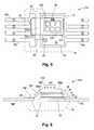
- FIGS. 1 and 2are top plan and side elevation views, respectively, of a prior art embodiment of an 8-lead standard outline integrated circuit (“SOIC-8”) lead frame-type of power MOSFET semiconductor device 10 that has a conductive metal strap 12 electrically connecting a semiconductor die 14 to a metal portion 16 B of a lead-frame-type substrate 16 .
- SOIC-8standard outline integrated circuit
- the drain terminals of one or more individual MOSFETs (not visualized) formed in the die 14are electrically connected to a metal or polysilicon first conductive layer 23 located on a downwardly-oriented first surface of the die.
- First conductive layer 23 ofis, in turn, electrically connected to the metal die paddle 20 of a first portion 16 A of the lead frame 16 by, e.g., a layer 22 of solder or an electrically conductive adhesive.
- the die paddle 20is integrally connected to each of four leads ( 5 - 8 ) of the first portion 16 A in this embodiment.
- the source terminals of the one or more individual MOSFETs in the die 14are connected to a metal or polysilicon second conductive layer 24 (FIG. 2) on an opposing upwardly oriented second surface of the die.
- the second conductive layer 24 on the die 14is electrically connected to a second portion 16 B of substrate 16 through an electrically conductive layer 36 , metal strap 12 , and electrically conductive layer 38 .
- Second portion 16 Bincludes leads 1 - 3 in this embodiment.
- the strap 12comprises a planar cover portion 30 at an inner first end thereof, a planar flange portion 34 at an opposite outer second end thereof, and an oblique connection portion 32 between cover portion 30 and flange portion 34 .
- Cover portion 30includes a first surface 30 a that is electrically connected to the second conductive layer 24 by electrically conductive layer 36 , and an opposite second surface 30 b that faces toward the top of the package when oriented as shown in FIG. 2 .
- Second surface 30 b and all other portions of strap 12are covered by encapsulant 18 .
- the flange portion 34 of the strap 12connects to the second portion 16 B of the substrate 16 by a lap joint using an electrically conductive layer 38 .
- the metal strap 12is made of a conductive metal, typically copper or a copper alloy. As illustrated in FIG. 2, with the device 10 oriented as shown, the first surface 30 a of the cover 30 and bottom surface of flange 34 portions of the strap 12 lap over the top surfaces of the die 14 and the second portion 16 B of the substrate 16 , respectively, and are respectively joined thereto with layers 36 , 38 of, e.g., solder or an electrically conductive epoxy.
- the gate terminals of the individual MOSFETsare connected to a third conductive layer, or gate pad 26 , located on the upper second surface of the die 14 (i.e., the same surface of die 14 as second conductive layer 24 ).
- the gate pad 26which is electrically isolated from the second conductive layer 24 , is electrically connected to a third portion 16 C of substrate 16 by a bond wire 28 (see FIG. 1 ).
- Third portion 16 Cincludes a lead 4 , and is electrically isolated from, but coplanar with, first and second portions 16 A and 16 B of substrate 16 .
- Encapsulant 18fully encloses die 14 and metal strap 12 , and encloses a portion of the lead frame substrate 16 , leaving the ends of leads 1 - 8 exposed for connection to other circuit components.
- Encapsulant 18is typically molded plastic.
- Pertinent dimensions of device 10include: an area of die 14 that is 2 by 2 to 8 by 8 mm ⁇ mm; a height of die 14 that is 0.2 to 0.3 mm; a height of cover portion 30 that is 0.1 to 0.2 mm; and a thickness of encapsulant 18 above second surface 30 b that is 0.1 to 0.3 mm.
- the width of strap 12is primarily a function of the area of die 14 and second conductive layer 24 .
- the length of strap 12is a function of the area of die 14 and second conductive layer 24 and the closeness of paddle 20 to second portion 16 B of substrate 16 .
- Metal strap 12 of device 10provides for improved thermal dissipation characteristics and lower electrical resistance in comparison to earlier configurations in which bond wires were used rather than metal strap 12 . Despite the improvements offered by the use of metal strap 12 , however, a need exists for a method and apparatus that provides an even greater degree of heat dissipation.
- the present inventionprovides methods and apparatuses for packaging a semiconductor die.
- the packagesprovide increased heat dissipation capabilities compared to prior art designs.
- a high power semiconductor dieis electrically connected to a substrate on which the die is mounted, e.g., a lead frame, with a metal strap.
- the die, substrate, and metal strapare encapsulated by an insulative, protective body in such a way that a portion of the metal strap is exposed to the outside environment.
- the exposed surfaceallows for increased thermal dissipation and less heat buildup during operation of the device.
- An exemplary method for making such a packageincludes the provision of a semiconductor die, an interconnective substrate, and a conductive metal strap. After the die, substrate, and metal strap are electrically interconnected, an insulative encapsulant is provided (e.g., by molding) over the die and portions of the substrate and strap in a manner that leaves an upper surface of the strap above the die exposed to the environment. In other embodiments, recesses may be formed in the exposed surface of the strap to further increase heat dissipation. In a further alternative embodiment, heat-radiating metal protrusions may be formed on, or fastened, to the exposed surface of the metal strap.
- a first surface of a metal strapis thermally connected, but not electrically connected, to an active surface of a memory, logic, or microprocessor die within rows of edge bond pads formed on the active surface of the die.
- An opposite surface of the strapis exposed to ambient through the encapsulant, which results in improved thermal dissipation.
- FIGS. 1 and 2are top plan and side elevation views, respectively, of a conventional power semiconductor device having a fully encapsulated metal strap that electrically connects a power MOSFET die therein to a substrate.
- FIGS. 3 and 4are top plan and side elevation views, respectively, of a semiconductor device having an exposed metal strap in accordance with one embodiment of the present invention.
- FIG. 5is a top plan view of a semiconductor device having an exposed metal strap in accordance with a second embodiment of the present invention, wherein recesses are formed in the exposed surface of the metal strap.
- FIG. 6is a side elevation view of a semiconductor device having an exposed metal strap in accordance with a third embodiment of the present invention, wherein heat-radiating protrusions are formed on the exposed surface of the metal strap.
- FIG. 7is a top plan view of a semiconductor device having an exposed metal strap in accordance with a fourth embodiment of the present invention.
- FIG. 8is a top plan view of a semiconductor device having an exposed metal strap in accordance with a fifth embodiment of the present invention.
- FIGS. 3 and 4show a first embodiment of a semiconductor device 110 within the present invention.
- the exemplar packagehas many of the same features as shown in FIGS. 1 and 2, except for changes to the metal strap 12 .
- Elements similar to those in the prior art device 10 illustrated in FIGS. 1 and 2are given the same identifying reference number.
- Metal strap 112 of FIGS. 3 and 4has a thicker cover portion 130 than strap 12 of FIGS. 1 and 2. Because cover portion 130 is thicker than cover portion 30 of FIGS. 1 and 2, surface 130 b of cover portion 130 is exposed through the nonconductive encapsulating body 118 . The exposed second surface 130 b of cover portion 130 radiates heat effectively to the exterior. In this instance, second surface 130 b is fully planar and is in the plane of the planar top surface of body 118 . For instance, where cover portion 30 of FIG. 2 had a height of between 0.1 to 0.2 mm, cover portion 130 may have a height of between 0.2 and 0.5 mm.
- the method of making device 110 of FIGS. 3 and 4is similar to the above described method of making device 10 , except for the molding step.
- Die 14 of FIG. 3is mounted on and electrically connected to die paddle 20 of first portion 16 A of substrate 16 and strap 112 is electrically and thermally connected to second conductive layer 24 of die 14 with an electrically and thermally conductive layer 36 (e.g., solder or silver-filled epoxy).
- encapsulant 18is molded in such a way that second surface 130 b of the cover portion 130 is exposed through an exterior surface of the plastic encapsulant 118 . This may be accomplished by abutting second surface 130 b of cover portion 130 of strap 112 against an inner wall of the top pocket of the mold.
- the thickness of cover portion 130is made to be sufficient to allow cover portion 130 to abut the inner wall of the mold pocket.
- strap 12 of FIGS. 1 and 2is used, but the thickness of encapsulant 18 above second surface 30 b of cover portion 30 is reduced so that second surface 30 b is exposed. This typically would require a shallower mold or some sort of a shim within the mold used to make device 10 of FIG. 1 .
- FIG. 5shows the top plan view of a semiconductor device 210 in accordance with another embodiment of the present invention.
- a side elevation viewis not shown but, similar to what is shown in FIG. 4, metal strap 212 has a thicker cover portion 230 than the prior art cover portion 30 of FIG. 1 .
- a matrix of square recesses 242are formed in the exposed second surface 230 b of the cover portion 230 of FIG. 5 .
- Recesses 242increase the surface area of cover portion 230 that is exposed to ambient for increased heat dissipation.
- a waffle pattern of recessesis shown, it is to be understood that the number of recesses, and their particular shape, orientation and dimensions can vary.
- FIG. 6shows a side elevation view of a packaged semiconductor device 310 of another embodiment of the present invention.
- the metal strap 312has a thicker cover portion 330 than the prior art device shown in FIGS. 1 and 2, and second surface 330 b of the cover portion 330 is exposed through the top of encapsulant 18 .
- fin-like vertical protrusions 340are formed on (or attached to) the exposed surface of the cover strap 330 and extend vertically from second surface 330 b for increased heat dissipation.
- the number, shape, size, and orientation of the protrusionsmay vary in other embodiments.
- FIG. 7shows a high power semiconductor device 410 .
- the differences between the embodiment of FIG. 7 and the embodiment of FIGS. 3 and 4include that, in FIG. 7, the die is inverted. In addition, the substrate is rearranged. As a result, bond wire 28 of FIG. 1 is eliminated.
- Die 14 of FIG. 7is a power MOSFET or some other three terminal device.
- a two terminal devicesuch a diode may be provided, which would eliminate the need for third portion 416 C of substrate 16 .
- die 14is inverted in FIG. 7 so that second conductive layer 24 (i.e., the source terminals) (not shown) faces and is electrically connected by conductive layer 22 to the juxtaposed die paddle 420 of second portion 416 B of substrate 416 , which includes integrally connected leads 1 - 3 .
- the gate pad 26faces and is electrically connected to a juxtaposed extension of third portion 416 C of substrate 416 .
- Third portion 416 Cis coplanar with, but electrically isolated from, first and second portions 416 A and 416 B of substrate 416 .
- Third portion 416 Cincludes a lead 4 that is electrically isolated from leads 1 - 3 and 5 - 8 .
- First conductive layer 23(i.e., the drain terminals) faces the top of the package in the embodiment of FIG. 7 .
- First conductive layer 23is electrically and thermally connected by an electrically and thermally conductive layer 36 (which may be solder or a filled electrically and thermally conductive epoxy or other adhesive) to planar first surface 430 a (not shown) of cover portion 430 of strap 412 .
- the opposing second surface 430 b of cover portion 430is exposed at the top of the package through the encapsulating body 18 .
- Recesses 442are provided in the form of three parallel rectilinear grooves that extend across second surface 430 b of cover portion 430 .
- Recesses 442increase the heat dissipation from cover portion 430 due to increased surface area and exposure to ambient. As above, the number, orientation, and dimensions of recesses 442 will vary. For example, the grooves may have tapered sidewalls. Alternatively, vertical fins may be provided on second surface 430 b , as in FIG. 6 .
- Metal strap 412 of FIG. 7includes a flange portion 434 opposite cover portion 430 and a connector portion that is between flange portion 434 and cover portion 430 .
- the connector portionhas an inner horizontal portion 432 a and an outer oblique portion 432 b in this embodiment.
- Flange portion 434is electrically connected to first portion 416 A of the substrate 416 by a conductive layer 38 (e.g., solder or a conductive adhesive such as silver-filled epoxy).
- First substrate portion 416 Aincludes one or more integrally connected leads (leads 5 - 8 in the embodiment illustrated).
- flange portion 434is set in a recess 440 that is formed in the upper surface of first portion 416 A of substrate 416 .
- Conductive layer 38attaches flange portion 434 to first portion 416 A within recess 440 .
- a hole 444is formed through flange portion 434 so that the material of layer 38 can wick upwards, thereby forming a key in hole 444 . Accordingly, a strong bond is formed.
- the above examples of the present inventioninvolved power devices, wherein the encapsulated die has conductive layers on its top and bottom surfaces that are electrically connected to the substrate and serve as input and output terminals for the device.
- the present inventionalso applies to other types of semiconductor devices, such as memory, logic, or microprocessor devices, that have an active surface with bond pads thereon and an opposing inactive surface.
- FIG. 8is a top plan view of a semiconductor device 500 having an exposed metal strap 212 , comprised of 230 b , 232 and 234 as shown in FIG. 5 .
- Device 500includes a semiconductor die 502 having several discrete conductive edge bond pads 504 on active upper first surface 506 of die 502 .
- An opposite inactive lower second surface (not shown) of die 502is attached to a planar metal die pad 510 using adhesive 513 , which may be electrically and/or thermally conductive.
- a plurality of leads 514surround die 502 .
- Conductive wires 516electrically connect some of the individual leads 514 to individual bond pads 504 , thereby providing input and output paths for die 502 .
- Metal strap 212comprised of 230 b , 232 and 234 of FIG. 8 is thermally connected to die 502 and some of the leads 514 .
- first surface 230 a (not shown) of cover portion 230 of strap 212is connected to first surface 506 of die 502 through a thermally conductive, but not electrically conductive, adhesive layer 536 that is attached to an insulated area of first surface 506 of die 502 .
- Layer 536may be diamond filled epoxy or an epoxy filled with some other thermally conductive, but not electrically conductive, material.
- An opposite second surface 230 b of cover portion 230is exposed at the top of the package through encapsulant 518 .
- strap 212conducts heat away from die 502 through exposed upper surface 230 b of cover portion 230 of strap 212 .
- flange portion 234 of strap 212is thermally connected to a metal bar 515 , which in turn is integrally connected to four leads 514 . Similar to FIG. 7, flange portion 234 is positioned in a groove 522 in bar 515 , and is thermally attached to bar 512 with a thermally conductive adhesive 520 . The opposing ends of the leads 514 extending from bar 515 may be thermally connected to a grounded heat sink.
- the lead frame substrate of FIGS. 3-7may be replaced by a single-piece, laminated substrate, such as a multi-layer printed circuit board (“PCB”), formed of layers of, e.g., epoxy-impregnated fiberglass and copper, with etched metal traces replacing the leads 1 - 8 .
- PCBprinted circuit board
- Solder ballstypically are fused to metallizations on the lower exposed surface of the PCB. Vias through the substrate electrically connect the solder balls to the metal traces. Accordingly, leads equivalent to leads 1 - 8 are formed of FIGS. 1-7 are formed.
- the methods described aboveare fully compatible with the techniques of high volume device production in which a plurality of identical devices are fabricated simultaneously in the form of a connected strip or array of devices that is subsequently encapsulated, and then cut apart, or “singulated,” into individual devices.
Landscapes
- Engineering & Computer Science (AREA)
- Computer Hardware Design (AREA)
- Microelectronics & Electronic Packaging (AREA)
- Power Engineering (AREA)
- Physics & Mathematics (AREA)
- Condensed Matter Physics & Semiconductors (AREA)
- General Physics & Mathematics (AREA)
- Lead Frames For Integrated Circuits (AREA)
Abstract
Description
Claims (19)
Priority Applications (2)
| Application Number | Priority Date | Filing Date | Title |
|---|---|---|---|
| US09/733,148US6566164B1 (en) | 2000-12-07 | 2000-12-07 | Exposed copper strap in a semiconductor package |
| US10/356,046US6723582B2 (en) | 2000-12-07 | 2003-01-31 | Method of making a semiconductor package having exposed metal strap |
Applications Claiming Priority (1)
| Application Number | Priority Date | Filing Date | Title |
|---|---|---|---|
| US09/733,148US6566164B1 (en) | 2000-12-07 | 2000-12-07 | Exposed copper strap in a semiconductor package |
Related Child Applications (1)
| Application Number | Title | Priority Date | Filing Date |
|---|---|---|---|
| US10/356,046DivisionUS6723582B2 (en) | 2000-12-07 | 2003-01-31 | Method of making a semiconductor package having exposed metal strap |
Publications (1)
| Publication Number | Publication Date |
|---|---|
| US6566164B1true US6566164B1 (en) | 2003-05-20 |
Family
ID=24946428
Family Applications (2)
| Application Number | Title | Priority Date | Filing Date |
|---|---|---|---|
| US09/733,148Expired - LifetimeUS6566164B1 (en) | 2000-12-07 | 2000-12-07 | Exposed copper strap in a semiconductor package |
| US10/356,046Expired - LifetimeUS6723582B2 (en) | 2000-12-07 | 2003-01-31 | Method of making a semiconductor package having exposed metal strap |
Family Applications After (1)
| Application Number | Title | Priority Date | Filing Date |
|---|---|---|---|
| US10/356,046Expired - LifetimeUS6723582B2 (en) | 2000-12-07 | 2003-01-31 | Method of making a semiconductor package having exposed metal strap |
Country Status (1)
| Country | Link |
|---|---|
| US (2) | US6566164B1 (en) |
Cited By (16)
| Publication number | Priority date | Publication date | Assignee | Title |
|---|---|---|---|---|
| US20020038904A1 (en)* | 1997-12-04 | 2002-04-04 | Hyundai Electronics Industries Co., Ltd. | Area array type semiconductor package and fabrication method |
| US20030038360A1 (en)* | 1999-02-17 | 2003-02-27 | Toshinori Hirashima | Semiconductor device and a method of manufacturing the same |
| US20040056362A1 (en)* | 2002-09-19 | 2004-03-25 | Kabushiki Kaisha Toshiba | Semiconductor device |
| US20050023670A1 (en)* | 2003-07-31 | 2005-02-03 | Renesas Technology Corp. | Semiconductor device and a method of manufacturing the same |
| US6873041B1 (en)* | 2001-11-07 | 2005-03-29 | Amkor Technology, Inc. | Power semiconductor package with strap |
| US20050287699A1 (en)* | 2004-06-23 | 2005-12-29 | Brauer Eric A | Electrical package employing segmented connector and solder joint |
| US20060049505A1 (en)* | 2002-12-10 | 2006-03-09 | Koninklijke Philips Electronics N.V. | High density interconnect power and ground strap and method therefor |
| US20060055027A1 (en)* | 2003-09-04 | 2006-03-16 | Makoto Kitabatake | Semiconductor device |
| US20060186516A1 (en)* | 2002-09-05 | 2006-08-24 | Kabushiki Kaisha Toshiba | Semiconductor device with semiconductor chip mounted in package |
| US20070044998A1 (en)* | 2005-08-26 | 2007-03-01 | Chan Aik H | Electronic package and circuit board having segmented contact pads |
| US20070176266A1 (en)* | 2005-12-15 | 2007-08-02 | Renesas Technology Corp. | Semiconductor device |
| US20090001559A1 (en)* | 2003-02-28 | 2009-01-01 | Renesas Technology Corp. | Semiconductor device, a method of manufacturing the same and an electronic device |
| US20090166850A1 (en)* | 2008-01-02 | 2009-07-02 | Oseob Jeon | High-Power Semiconductor Die Packages With Integrated Heat-Sink Capability and Methods of Manufacturing the Same |
| US8531016B2 (en) | 2011-05-19 | 2013-09-10 | International Rectifier Corporation | Thermally enhanced semiconductor package with exposed parallel conductive clip |
| CN104821304A (en)* | 2014-01-31 | 2015-08-05 | 株式会社东芝 | Semiconductor device and manufacturing method of the same |
| US9414528B2 (en) | 2014-11-06 | 2016-08-09 | International Business Machines Corporation | Thermal spreading for an externally pluggable electronic module |
Families Citing this family (23)
| Publication number | Priority date | Publication date | Assignee | Title |
|---|---|---|---|---|
| US6784540B2 (en)* | 2001-10-10 | 2004-08-31 | International Rectifier Corp. | Semiconductor device package with improved cooling |
| US7034385B2 (en)* | 2003-08-05 | 2006-04-25 | International Rectifier Corporation | Topless semiconductor package |
| US8390131B2 (en)* | 2004-06-03 | 2013-03-05 | International Rectifier Corporation | Semiconductor device with reduced contact resistance |
| US7084494B2 (en)* | 2004-06-18 | 2006-08-01 | Texas Instruments Incorporated | Semiconductor package having integrated metal parts for thermal enhancement |
| US7759775B2 (en)* | 2004-07-20 | 2010-07-20 | Alpha And Omega Semiconductor Incorporated | High current semiconductor power device SOIC package |
| JP2006173437A (en)* | 2004-12-17 | 2006-06-29 | Toshiba Corp | Semiconductor device |
| DE102005011159B4 (en)* | 2005-03-09 | 2013-05-16 | Infineon Technologies Ag | Semiconductor device having surface mount external contact pads and method of making the same |
| US7230333B2 (en) | 2005-04-21 | 2007-06-12 | International Rectifier Corporation | Semiconductor package |
| US7504733B2 (en) | 2005-08-17 | 2009-03-17 | Ciclon Semiconductor Device Corp. | Semiconductor die package |
| US7560808B2 (en)* | 2005-10-19 | 2009-07-14 | Texas Instruments Incorporated | Chip scale power LDMOS device |
| US7446375B2 (en)* | 2006-03-14 | 2008-11-04 | Ciclon Semiconductor Device Corp. | Quasi-vertical LDMOS device having closed cell layout |
| US20080036078A1 (en)* | 2006-08-14 | 2008-02-14 | Ciclon Semiconductor Device Corp. | Wirebond-less semiconductor package |
| US8138587B2 (en) | 2008-09-30 | 2012-03-20 | Infineon Technologies Ag | Device including two mounting surfaces |
| US8049312B2 (en)* | 2009-01-12 | 2011-11-01 | Texas Instruments Incorporated | Semiconductor device package and method of assembly thereof |
| US8344464B2 (en) | 2011-05-19 | 2013-01-01 | International Rectifier Corporation | Multi-transistor exposed conductive clip for high power semiconductor packages |
| JP2013258387A (en)* | 2012-05-15 | 2013-12-26 | Rohm Co Ltd | Power-module semiconductor device |
| US20140001480A1 (en)* | 2012-07-02 | 2014-01-02 | Infineon Technologies Ag | Lead Frame Packages and Methods of Formation Thereof |
| US9478484B2 (en)* | 2012-10-19 | 2016-10-25 | Infineon Technologies Austria Ag | Semiconductor packages and methods of formation thereof |
| JP2015144217A (en)* | 2014-01-31 | 2015-08-06 | 株式会社東芝 | Connector frame and semiconductor device |
| US11088046B2 (en) | 2018-06-25 | 2021-08-10 | Semiconductor Components Industries, Llc | Semiconductor device package with clip interconnect and dual side cooling |
| DE102019206824A1 (en)* | 2019-05-10 | 2020-11-12 | Robert Bosch Gmbh | Contact arrangement and power module |
| JP7266508B2 (en)* | 2019-10-21 | 2023-04-28 | ルネサスエレクトロニクス株式会社 | semiconductor equipment |
| US20240113064A1 (en)* | 2022-09-29 | 2024-04-04 | Stmicroelectronics, Inc. | Power leadframe package with reduced solder voids |
Citations (44)
| Publication number | Priority date | Publication date | Assignee | Title |
|---|---|---|---|---|
| GB720225A (en) | 1951-07-17 | 1954-12-15 | Standard Telephones Cables Ltd | Improvements in or relating to radio receivers having a built-in antenna |
| GB720234A (en) | 1952-09-01 | 1954-12-15 | Victor Kiernan Scavullo | Improvements in or relating to the manufacture of metal hollow-ware |
| US4189342A (en) | 1971-10-07 | 1980-02-19 | U.S. Philips Corporation | Semiconductor device comprising projecting contact layers |
| JPS5745959A (en) | 1980-09-02 | 1982-03-16 | Nec Corp | Resin-sealed semiconductor device |
| JPS60116239A (en) | 1983-11-28 | 1985-06-22 | Nec Corp | Radio communication equipment |
| JPS6139555A (en) | 1984-07-31 | 1986-02-25 | Toshiba Corp | Resin sealed type semiconductor device with heat sink |
| WO1988002929A1 (en) | 1986-10-14 | 1988-04-21 | Hughes Aircraft Company | Low resistance electrical interconnection for synchronous rectifiers |
| JPS63233555A (en) | 1987-03-23 | 1988-09-29 | Toshiba Corp | Resin-encapsulated semiconductor device |
| US4935803A (en) | 1988-09-09 | 1990-06-19 | Motorola, Inc. | Self-centering electrode for power devices |
| US4942452A (en) | 1987-02-25 | 1990-07-17 | Hitachi, Ltd. | Lead frame and semiconductor device |
| US4987478A (en) | 1990-02-20 | 1991-01-22 | Unisys Corporation | Micro individual integrated circuit package |
| US5041902A (en) | 1989-12-14 | 1991-08-20 | Motorola, Inc. | Molded electronic package with compression structures |
| US5218231A (en) | 1989-08-30 | 1993-06-08 | Kabushiki Kaisha Toshiba | Mold-type semiconductor device |
| US5266834A (en) | 1989-03-13 | 1993-11-30 | Hitachi Ltd. | Semiconductor device and an electronic device with the semiconductor devices mounted thereon |
| US5278446A (en) | 1992-07-06 | 1994-01-11 | Motorola, Inc. | Reduced stress plastic package |
| US5328870A (en) | 1992-01-17 | 1994-07-12 | Amkor Electronics, Inc. | Method for forming plastic molded package with heat sink for integrated circuit devices |
| US5477160A (en) | 1992-08-12 | 1995-12-19 | Fujitsu Limited | Module test card |
| JPH0864634A (en) | 1994-08-23 | 1996-03-08 | Hitachi Ltd | Semiconductor device and manufacturing method thereof |
| US5544412A (en) | 1994-05-24 | 1996-08-13 | Motorola, Inc. | Method for coupling a power lead to a bond pad in an electronic module |
| US5663597A (en) | 1992-10-26 | 1997-09-02 | Texas Instruments Incorporated | RF device package for high frequency applications |
| US5665996A (en) | 1994-12-30 | 1997-09-09 | Siliconix Incorporated | Vertical power mosfet having thick metal layer to reduce distributed resistance |
| US5701034A (en) | 1994-05-03 | 1997-12-23 | Amkor Electronics, Inc. | Packaged semiconductor die including heat sink with locking feature |
| US5708567A (en) | 1995-11-15 | 1998-01-13 | Anam Industrial Co., Ltd. | Ball grid array semiconductor package with ring-type heat sink |
| US5731709A (en)* | 1996-01-26 | 1998-03-24 | Motorola, Inc. | Method for testing a ball grid array semiconductor device and a device for such testing |
| US5767527A (en) | 1994-07-07 | 1998-06-16 | Fujitsu Limited | Semiconductor device suitable for testing |
| US5807768A (en) | 1995-09-04 | 1998-09-15 | Anam Industrial Co., Ltd. | Method for fabricating a heat sink-integrated semiconductor package |
| US5814884A (en) | 1996-10-24 | 1998-09-29 | International Rectifier Corporation | Commonly housed diverse semiconductor die |
| US5854511A (en) | 1995-11-17 | 1998-12-29 | Anam Semiconductor, Inc. | Semiconductor package including heat sink with layered conductive plate and non-conductive tape bonding to leads |
| US5866949A (en)* | 1996-12-02 | 1999-02-02 | Minnesota Mining And Manufacturing Company | Chip scale ball grid array for integrated circuit packaging |
| US5877043A (en) | 1996-02-01 | 1999-03-02 | International Business Machines Corporation | Electronic package with strain relief means and method of making |
| US6028354A (en) | 1997-10-14 | 2000-02-22 | Amkor Technology, Inc. | Microelectronic device package having a heat sink structure for increasing the thermal conductivity of the package |
| US6040626A (en) | 1998-09-25 | 2000-03-21 | International Rectifier Corp. | Semiconductor package |
| US6127727A (en) | 1998-04-06 | 2000-10-03 | Delco Electronics Corp. | Semiconductor substrate subassembly with alignment and stress relief features |
| US6144093A (en) | 1998-04-27 | 2000-11-07 | International Rectifier Corp. | Commonly housed diverse semiconductor die with reduced inductance |
| US6187611B1 (en) | 1998-10-23 | 2001-02-13 | Microsemi Microwave Products, Inc. | Monolithic surface mount semiconductor device and method for fabricating same |
| US6223429B1 (en) | 1995-06-13 | 2001-05-01 | Hitachi Chemical Company, Ltd. | Method of production of semiconductor device |
| US6229204B1 (en) | 1998-09-03 | 2001-05-08 | Micron Technology, Inc. | Chip on board with heat sink attachment |
| US6242283B1 (en)* | 1999-12-30 | 2001-06-05 | Siliconware Precision Industries Co., Ltd. | Wafer level packaging process of semiconductor |
| US6249041B1 (en) | 1998-06-02 | 2001-06-19 | Siliconix Incorporated | IC chip package with directly connected leads |
| US6252300B1 (en) | 1999-01-14 | 2001-06-26 | United Microelectronics Corp. | Direct contact through hole type wafer structure |
| US6256200B1 (en) | 1999-05-27 | 2001-07-03 | Allen K. Lam | Symmetrical package for semiconductor die |
| US6255672B1 (en) | 1997-11-26 | 2001-07-03 | Kabushiki Kaisha Toshiba | Semiconductor device |
| US6306680B1 (en)* | 1999-02-22 | 2001-10-23 | General Electric Company | Power overlay chip scale packages for discrete power devices |
| US6309916B1 (en)* | 1999-11-17 | 2001-10-30 | Amkor Technology, Inc | Method of molding plastic semiconductor packages |
Family Cites Families (2)
| Publication number | Priority date | Publication date | Assignee | Title |
|---|---|---|---|---|
| US5767546A (en) | 1994-12-30 | 1998-06-16 | Siliconix Incorporated | Laternal power mosfet having metal strap layer to reduce distributed resistance |
| US6319755B1 (en)* | 1999-12-01 | 2001-11-20 | Amkor Technology, Inc. | Conductive strap attachment process that allows electrical connector between an integrated circuit die and leadframe |
- 2000
- 2000-12-07USUS09/733,148patent/US6566164B1/ennot_activeExpired - Lifetime
- 2003
- 2003-01-31USUS10/356,046patent/US6723582B2/ennot_activeExpired - Lifetime
Patent Citations (47)
| Publication number | Priority date | Publication date | Assignee | Title |
|---|---|---|---|---|
| GB720225A (en) | 1951-07-17 | 1954-12-15 | Standard Telephones Cables Ltd | Improvements in or relating to radio receivers having a built-in antenna |
| GB720234A (en) | 1952-09-01 | 1954-12-15 | Victor Kiernan Scavullo | Improvements in or relating to the manufacture of metal hollow-ware |
| US4189342A (en) | 1971-10-07 | 1980-02-19 | U.S. Philips Corporation | Semiconductor device comprising projecting contact layers |
| JPS5745959A (en) | 1980-09-02 | 1982-03-16 | Nec Corp | Resin-sealed semiconductor device |
| JPS60116239A (en) | 1983-11-28 | 1985-06-22 | Nec Corp | Radio communication equipment |
| JPS6139555A (en) | 1984-07-31 | 1986-02-25 | Toshiba Corp | Resin sealed type semiconductor device with heat sink |
| WO1988002929A1 (en) | 1986-10-14 | 1988-04-21 | Hughes Aircraft Company | Low resistance electrical interconnection for synchronous rectifiers |
| US4942452A (en) | 1987-02-25 | 1990-07-17 | Hitachi, Ltd. | Lead frame and semiconductor device |
| JPS63233555A (en) | 1987-03-23 | 1988-09-29 | Toshiba Corp | Resin-encapsulated semiconductor device |
| US4935803A (en) | 1988-09-09 | 1990-06-19 | Motorola, Inc. | Self-centering electrode for power devices |
| US5266834A (en) | 1989-03-13 | 1993-11-30 | Hitachi Ltd. | Semiconductor device and an electronic device with the semiconductor devices mounted thereon |
| US5218231A (en) | 1989-08-30 | 1993-06-08 | Kabushiki Kaisha Toshiba | Mold-type semiconductor device |
| US5041902A (en) | 1989-12-14 | 1991-08-20 | Motorola, Inc. | Molded electronic package with compression structures |
| US4987478A (en) | 1990-02-20 | 1991-01-22 | Unisys Corporation | Micro individual integrated circuit package |
| US5328870A (en) | 1992-01-17 | 1994-07-12 | Amkor Electronics, Inc. | Method for forming plastic molded package with heat sink for integrated circuit devices |
| US5455462A (en) | 1992-01-17 | 1995-10-03 | Amkor Electronics, Inc. | Plastic molded package with heat sink for integrated circuit devices |
| US5278446A (en) | 1992-07-06 | 1994-01-11 | Motorola, Inc. | Reduced stress plastic package |
| US5477160A (en) | 1992-08-12 | 1995-12-19 | Fujitsu Limited | Module test card |
| US5663597A (en) | 1992-10-26 | 1997-09-02 | Texas Instruments Incorporated | RF device package for high frequency applications |
| US5701034A (en) | 1994-05-03 | 1997-12-23 | Amkor Electronics, Inc. | Packaged semiconductor die including heat sink with locking feature |
| US5722161A (en) | 1994-05-03 | 1998-03-03 | Amkor Electronics, Inc. | Method of making a packaged semiconductor die including heat sink with locking feature |
| US5544412A (en) | 1994-05-24 | 1996-08-13 | Motorola, Inc. | Method for coupling a power lead to a bond pad in an electronic module |
| US5767527A (en) | 1994-07-07 | 1998-06-16 | Fujitsu Limited | Semiconductor device suitable for testing |
| JPH0864634A (en) | 1994-08-23 | 1996-03-08 | Hitachi Ltd | Semiconductor device and manufacturing method thereof |
| US5665996A (en) | 1994-12-30 | 1997-09-09 | Siliconix Incorporated | Vertical power mosfet having thick metal layer to reduce distributed resistance |
| US6223429B1 (en) | 1995-06-13 | 2001-05-01 | Hitachi Chemical Company, Ltd. | Method of production of semiconductor device |
| US5807768A (en) | 1995-09-04 | 1998-09-15 | Anam Industrial Co., Ltd. | Method for fabricating a heat sink-integrated semiconductor package |
| US5708567A (en) | 1995-11-15 | 1998-01-13 | Anam Industrial Co., Ltd. | Ball grid array semiconductor package with ring-type heat sink |
| US5854511A (en) | 1995-11-17 | 1998-12-29 | Anam Semiconductor, Inc. | Semiconductor package including heat sink with layered conductive plate and non-conductive tape bonding to leads |
| US5731709A (en)* | 1996-01-26 | 1998-03-24 | Motorola, Inc. | Method for testing a ball grid array semiconductor device and a device for such testing |
| US5877043A (en) | 1996-02-01 | 1999-03-02 | International Business Machines Corporation | Electronic package with strain relief means and method of making |
| US5814884A (en) | 1996-10-24 | 1998-09-29 | International Rectifier Corporation | Commonly housed diverse semiconductor die |
| US5814884C1 (en) | 1996-10-24 | 2002-01-29 | Int Rectifier Corp | Commonly housed diverse semiconductor die |
| US5866949A (en)* | 1996-12-02 | 1999-02-02 | Minnesota Mining And Manufacturing Company | Chip scale ball grid array for integrated circuit packaging |
| US6028354A (en) | 1997-10-14 | 2000-02-22 | Amkor Technology, Inc. | Microelectronic device package having a heat sink structure for increasing the thermal conductivity of the package |
| US6255672B1 (en) | 1997-11-26 | 2001-07-03 | Kabushiki Kaisha Toshiba | Semiconductor device |
| US6127727A (en) | 1998-04-06 | 2000-10-03 | Delco Electronics Corp. | Semiconductor substrate subassembly with alignment and stress relief features |
| US6144093A (en) | 1998-04-27 | 2000-11-07 | International Rectifier Corp. | Commonly housed diverse semiconductor die with reduced inductance |
| US6249041B1 (en) | 1998-06-02 | 2001-06-19 | Siliconix Incorporated | IC chip package with directly connected leads |
| US6229204B1 (en) | 1998-09-03 | 2001-05-08 | Micron Technology, Inc. | Chip on board with heat sink attachment |
| US6040626A (en) | 1998-09-25 | 2000-03-21 | International Rectifier Corp. | Semiconductor package |
| US6187611B1 (en) | 1998-10-23 | 2001-02-13 | Microsemi Microwave Products, Inc. | Monolithic surface mount semiconductor device and method for fabricating same |
| US6252300B1 (en) | 1999-01-14 | 2001-06-26 | United Microelectronics Corp. | Direct contact through hole type wafer structure |
| US6306680B1 (en)* | 1999-02-22 | 2001-10-23 | General Electric Company | Power overlay chip scale packages for discrete power devices |
| US6256200B1 (en) | 1999-05-27 | 2001-07-03 | Allen K. Lam | Symmetrical package for semiconductor die |
| US6309916B1 (en)* | 1999-11-17 | 2001-10-30 | Amkor Technology, Inc | Method of molding plastic semiconductor packages |
| US6242283B1 (en)* | 1999-12-30 | 2001-06-05 | Siliconware Precision Industries Co., Ltd. | Wafer level packaging process of semiconductor |
Non-Patent Citations (3)
| Title |
|---|
| http://www.siliconix.com, "New Package Technology Yields Nearly Twofold Improvement Over Previous State-of-the-Art," Vishay Siliconix Press Release, Dec. 9, 1998. |
| Internet Website Article, Electronic Design-Mar. 22, 1999, vol. 47, No. 6- MOSFETs Break Out Of The Shackles Of Wirebonding. |
| Provisional Patent Application No. 60/101810. |
Cited By (44)
| Publication number | Priority date | Publication date | Assignee | Title |
|---|---|---|---|---|
| US20020038904A1 (en)* | 1997-12-04 | 2002-04-04 | Hyundai Electronics Industries Co., Ltd. | Area array type semiconductor package and fabrication method |
| US7122401B2 (en)* | 1997-12-04 | 2006-10-17 | Hyundai Electronics Industries Co., Ltd. | Area array type semiconductor package fabrication method |
| US7812464B2 (en) | 1999-02-17 | 2010-10-12 | Renesas Electronics Corporation | Semiconductor device and a method of manufacturing for high output MOSFET |
| US6812554B2 (en)* | 1999-02-17 | 2004-11-02 | Renesas Technology Corp. | Semiconductor device and a method of manufacturing the same |
| US20050023671A1 (en)* | 1999-02-17 | 2005-02-03 | Renesas Technology Corp. | Semiconductor device and a method of manufacturing the same |
| US20080211082A1 (en)* | 1999-02-17 | 2008-09-04 | Hitachi, Ltd. | Semiconductor device and a method of manufacturing the same |
| US20030038360A1 (en)* | 1999-02-17 | 2003-02-27 | Toshinori Hirashima | Semiconductor device and a method of manufacturing the same |
| US7385279B2 (en) | 1999-02-17 | 2008-06-10 | Renesas Technology Corp. | Semiconductor device and a method of manufacturing the same |
| US20070158819A1 (en)* | 1999-02-17 | 2007-07-12 | Toshinori Hirashima | Semiconductor device and a method of manufacturing the same |
| US7160760B2 (en) | 1999-02-17 | 2007-01-09 | Renesas Technology Corp. | Semiconductor device and a method of manufacturing the same |
| US6873041B1 (en)* | 2001-11-07 | 2005-03-29 | Amkor Technology, Inc. | Power semiconductor package with strap |
| US7554210B2 (en)* | 2002-09-05 | 2009-06-30 | Kabushiki Kaisha Toshiba | Semiconductor device with semiconductor chip mounted in package |
| US20060186516A1 (en)* | 2002-09-05 | 2006-08-24 | Kabushiki Kaisha Toshiba | Semiconductor device with semiconductor chip mounted in package |
| US6768188B2 (en)* | 2002-09-19 | 2004-07-27 | Kabushiki Kaisha Toshiba | Semiconductor device |
| US20040056362A1 (en)* | 2002-09-19 | 2004-03-25 | Kabushiki Kaisha Toshiba | Semiconductor device |
| US20060049505A1 (en)* | 2002-12-10 | 2006-03-09 | Koninklijke Philips Electronics N.V. | High density interconnect power and ground strap and method therefor |
| US7728416B2 (en)* | 2003-02-28 | 2010-06-01 | Renesas Technology Corp. | Semiconductor device, a method of manufacturing the same and an electronic device |
| US20090001559A1 (en)* | 2003-02-28 | 2009-01-01 | Renesas Technology Corp. | Semiconductor device, a method of manufacturing the same and an electronic device |
| US20100193934A1 (en)* | 2003-02-28 | 2010-08-05 | Renesas Technology Corp. | Semiconductor device, a method of manufacturing the same and an electronic device |
| US8022518B2 (en) | 2003-02-28 | 2011-09-20 | Renesas Electronics Corporation | Semiconductor device having a sealing body and partially exposed conductors |
| US8698289B2 (en) | 2003-02-28 | 2014-04-15 | Renesas Electronics Corporation | Semiconductor device, a method of manufacturing the same and an electronic device |
| US7408251B2 (en) | 2003-07-31 | 2008-08-05 | Renesas Technology Corp. | Semiconductor packaging device comprising a semiconductor chip including a MOSFET |
| US20050023670A1 (en)* | 2003-07-31 | 2005-02-03 | Renesas Technology Corp. | Semiconductor device and a method of manufacturing the same |
| US6992386B2 (en)* | 2003-07-31 | 2006-01-31 | Renesas Technology Corp. | Semiconductor device and a method of manufacturing the same |
| US20080272472A1 (en)* | 2003-07-31 | 2008-11-06 | Renesas Technology Corp. | Semiconductor packaging device comprising a semiconductor chip including a MOSFET |
| US20060097391A1 (en)* | 2003-07-31 | 2006-05-11 | Renesas Technology Corp. | Semiconductor device and a method of manufacturing the same |
| US7586180B2 (en) | 2003-07-31 | 2009-09-08 | Renesas Technology Corp. | Semiconductor packaging device comprising a semiconductor chip including a MOSFET |
| US7786565B2 (en)* | 2003-09-04 | 2010-08-31 | Panasonic Corporation | Semiconductor apparatus including power semiconductor device constructed by using wide band gap semiconductor |
| US20060055027A1 (en)* | 2003-09-04 | 2006-03-16 | Makoto Kitabatake | Semiconductor device |
| US7049171B2 (en) | 2004-06-23 | 2006-05-23 | Delphi Technologies, Inc. | Electrical package employing segmented connector and solder joint |
| US20050287699A1 (en)* | 2004-06-23 | 2005-12-29 | Brauer Eric A | Electrical package employing segmented connector and solder joint |
| US20070044998A1 (en)* | 2005-08-26 | 2007-03-01 | Chan Aik H | Electronic package and circuit board having segmented contact pads |
| US7280370B2 (en) | 2005-08-26 | 2007-10-09 | Delphi Technologies, Inc. | Electronic package and circuit board having segmented contact pads |
| US20110156274A1 (en)* | 2005-12-15 | 2011-06-30 | Renesas Technology Corp. | Semiconductor device |
| US20070176266A1 (en)* | 2005-12-15 | 2007-08-02 | Renesas Technology Corp. | Semiconductor device |
| US7800219B2 (en)* | 2008-01-02 | 2010-09-21 | Fairchild Semiconductor Corporation | High-power semiconductor die packages with integrated heat-sink capability and methods of manufacturing the same |
| US20110059580A1 (en)* | 2008-01-02 | 2011-03-10 | Oseob Jeon | High-power semiconductor die packages with integrated heat-sink capability and methods of manufacturing the same |
| US8193043B2 (en) | 2008-01-02 | 2012-06-05 | Fairchild Semiconductor Corporation | High-power semiconductor die packages with integrated heat-sink capability and methods of manufacturing the same |
| US20090166850A1 (en)* | 2008-01-02 | 2009-07-02 | Oseob Jeon | High-Power Semiconductor Die Packages With Integrated Heat-Sink Capability and Methods of Manufacturing the Same |
| US8531016B2 (en) | 2011-05-19 | 2013-09-10 | International Rectifier Corporation | Thermally enhanced semiconductor package with exposed parallel conductive clip |
| CN104821304A (en)* | 2014-01-31 | 2015-08-05 | 株式会社东芝 | Semiconductor device and manufacturing method of the same |
| US20150221580A1 (en)* | 2014-01-31 | 2015-08-06 | Kabushiki Kaisha Toshiba | Semiconductor device and manufacturing method of the same |
| US9414528B2 (en) | 2014-11-06 | 2016-08-09 | International Business Machines Corporation | Thermal spreading for an externally pluggable electronic module |
| US9414527B2 (en) | 2014-11-06 | 2016-08-09 | International Business Machines Corporation | Thermal spreading for an externally pluggable electronic module |
Also Published As
| Publication number | Publication date |
|---|---|
| US20030113954A1 (en) | 2003-06-19 |
| US6723582B2 (en) | 2004-04-20 |
Similar Documents
| Publication | Publication Date | Title |
|---|---|---|
| US6566164B1 (en) | Exposed copper strap in a semiconductor package | |
| US6781242B1 (en) | Thin ball grid array package | |
| US7208818B2 (en) | Power semiconductor package | |
| US6777800B2 (en) | Semiconductor die package including drain clip | |
| US6873041B1 (en) | Power semiconductor package with strap | |
| US7781265B2 (en) | DFN semiconductor package having reduced electrical resistance | |
| US6853070B2 (en) | Die-down ball grid array package with die-attached heat spreader and method for making the same | |
| US7508060B2 (en) | Multi-chip semiconductor connector assemblies | |
| US20090230540A1 (en) | High performance multi-chip flip chip package | |
| US6614660B1 (en) | Thermally enhanced IC chip package | |
| US20100193922A1 (en) | Semiconductor chip package | |
| US7633140B2 (en) | Inverted J-lead for power devices | |
| US7692276B2 (en) | Thermally enhanced ball grid array package formed in strip with one-piece die-attached exposed heat spreader | |
| CN1711639B (en) | Folded flexible bondwire-less multi-chip power package | |
| US5939781A (en) | Thermally enhanced integrated circuit packaging system | |
| US7566967B2 (en) | Semiconductor package structure for vertical mount and method | |
| US7102211B2 (en) | Semiconductor device and hybrid integrated circuit device | |
| US20060145312A1 (en) | Dual flat non-leaded semiconductor package | |
| US20050194698A1 (en) | Integrated circuit package with keep-out zone overlapping undercut zone | |
| US7951651B2 (en) | Dual flat non-leaded semiconductor package | |
| US11715676B2 (en) | Semiconductor device | |
| KR100212392B1 (en) | Semiconductor package | |
| US9040356B2 (en) | Semiconductor including cup-shaped leadframe packaging techniques | |
| CN119419196A (en) | Packaging structure and forming method thereof | |
| EP1353375A1 (en) | A thermally enhanced IC chip package |
Legal Events
| Date | Code | Title | Description |
|---|---|---|---|
| AS | Assignment | Owner name:AMKOR TECHNOLOGY, INC., ARIZONA Free format text:ASSIGNMENT OF ASSIGNORS INTEREST;ASSIGNORS:GLENN, THOMAS P.;GILLETT, BLAKE A.;REEL/FRAME:011361/0184;SIGNING DATES FROM 20001127 TO 20001128 | |
| STCF | Information on status: patent grant | Free format text:PATENTED CASE | |
| AS | Assignment | Owner name:CITICORP NORTH AMERICA, INC. AS ADMINISTRATIVE AGE Free format text:SECURITY AGREEMENT;ASSIGNORS:AMKOR TECHNOLOGY, INC.;GUARDIAN ASSETS, INC.;REEL/FRAME:014885/0691 Effective date:20040629 | |
| AS | Assignment | Owner name:CITICORP NORTH AMERICA, INC. AS "AGENT", NEW YORK Free format text:SECURITY AGREEMENT;ASSIGNORS:AMKOR TECHNOLOGY, INC.;GUARDIAN ASSETS, INC.;REEL/FRAME:015942/0521 Effective date:20041027 | |
| AS | Assignment | Owner name:BANK OF AMERICA, N.A., TEXAS Free format text:SECURITY AGREEMENT;ASSIGNOR:AMKOR TECHNOLOGY, INC.;REEL/FRAME:017379/0630 Effective date:20051123 Owner name:AMKOR TECHNOLOGY, INC., ARIZONA Free format text:TERMINATION & RELEASE OF PATENT SECURITY AGREEMENT;ASSIGNOR:CITICORP NORTH AMERICA, INC.;REEL/FRAME:017388/0868 Effective date:20051128 | |
| FPAY | Fee payment | Year of fee payment:4 | |
| FPAY | Fee payment | Year of fee payment:8 | |
| FPAY | Fee payment | Year of fee payment:12 | |
| AS | Assignment | Owner name:BANK OF AMERICA, N.A., AS AGENT, CALIFORNIA Free format text:SECURITY INTEREST;ASSIGNOR:AMKOR TECHNOLOGY, INC.;REEL/FRAME:046683/0139 Effective date:20180713 | |
| AS | Assignment | Owner name:AMKOR TECHNOLOGY SINGAPORE HOLDING PTE.LTD., SINGAPORE Free format text:ASSIGNMENT OF ASSIGNORS INTEREST;ASSIGNOR:AMKOR TECHNOLOGY, INC.;REEL/FRAME:054067/0135 Effective date:20191119 |