US6564269B1 - Bi-directional data transfer using the video blanking period in a digital data stream - Google Patents
Bi-directional data transfer using the video blanking period in a digital data streamDownload PDFInfo
- Publication number
- US6564269B1 US6564269B1US09/392,229US39222999AUS6564269B1US 6564269 B1US6564269 B1US 6564269B1US 39222999 AUS39222999 AUS 39222999AUS 6564269 B1US6564269 B1US 6564269B1
- Authority
- US
- United States
- Prior art keywords
- data
- processor
- digital
- transmitting
- pixel data
- Prior art date
- Legal status (The legal status is an assumption and is not a legal conclusion. Google has not performed a legal analysis and makes no representation as to the accuracy of the status listed.)
- Expired - Lifetime
Links
Images


Classifications
- G—PHYSICS
- G06—COMPUTING OR CALCULATING; COUNTING
- G06F—ELECTRIC DIGITAL DATA PROCESSING
- G06F3/00—Input arrangements for transferring data to be processed into a form capable of being handled by the computer; Output arrangements for transferring data from processing unit to output unit, e.g. interface arrangements
- G06F3/14—Digital output to display device ; Cooperation and interconnection of the display device with other functional units
- G—PHYSICS
- G09—EDUCATION; CRYPTOGRAPHY; DISPLAY; ADVERTISING; SEALS
- G09G—ARRANGEMENTS OR CIRCUITS FOR CONTROL OF INDICATING DEVICES USING STATIC MEANS TO PRESENT VARIABLE INFORMATION
- G09G5/00—Control arrangements or circuits for visual indicators common to cathode-ray tube indicators and other visual indicators
- G09G5/003—Details of a display terminal, the details relating to the control arrangement of the display terminal and to the interfaces thereto
- G09G5/006—Details of the interface to the display terminal
- H—ELECTRICITY
- H04—ELECTRIC COMMUNICATION TECHNIQUE
- H04N—PICTORIAL COMMUNICATION, e.g. TELEVISION
- H04N11/00—Colour television systems
- H04N11/04—Colour television systems using pulse code modulation
- H04N11/042—Codec means
- H—ELECTRICITY
- H04—ELECTRIC COMMUNICATION TECHNIQUE
- H04N—PICTORIAL COMMUNICATION, e.g. TELEVISION
- H04N7/00—Television systems
- H04N7/08—Systems for the simultaneous or sequential transmission of more than one television signal, e.g. additional information signals, the signals occupying wholly or partially the same frequency band, e.g. by time division
- H04N7/083—Systems for the simultaneous or sequential transmission of more than one television signal, e.g. additional information signals, the signals occupying wholly or partially the same frequency band, e.g. by time division with signal insertion during the vertical and the horizontal blanking interval, e.g. MAC data signals
- G—PHYSICS
- G09—EDUCATION; CRYPTOGRAPHY; DISPLAY; ADVERTISING; SEALS
- G09G—ARRANGEMENTS OR CIRCUITS FOR CONTROL OF INDICATING DEVICES USING STATIC MEANS TO PRESENT VARIABLE INFORMATION
- G09G2370/00—Aspects of data communication
- G09G2370/04—Exchange of auxiliary data, i.e. other than image data, between monitor and graphics controller
Definitions
- Most computer systemsconsist of a processor unit and a number of peripheral devices coupled to the processor unit.
- the peripheral devicessend and receive information to and from the processor and, typically, each peripheral device is separately connected to the processor unit by an individual set of cables, with each set of cables having a number of wires.
- the wiresmay be used for transferring information from the processor unit to the peripheral, as in the case of digital pixel data transferred to an active matrix flat panel display; or, the wires may used for transferring digital information from the peripherals to the processor unit, as in the case of digital data transferred from a keyboard or mouse to the processor unit.
- the informationmay be transferred serially or in parallel, depending upon the number of wires and the communications protocol used to transmit the information.
- FIG. 1illustrates a conventional computer system 100 having a processor unit 101 and a number of peripherals coupled to the processor.
- the peripheralsinclude a keyboard 102 , a mouse 103 , a display 104 , a digital camera 105 , and a pair of speakers 106 a and 106 b.
- each of the peripheralsis coupled to the processor unit through an individual cable assembly.
- the display 104is coupled to the processor 101 through cable assembly 110
- the keyboard 102is coupled to the processor 101 through cable assembly 111
- the mouse 103is coupled to the processor 101 through cable assembly 112
- the digital camera 105is coupled to the processor 101 through cable assembly 114
- the pair of speakers 106 a and 106 bare coupled to the processor 101 through cable assemblies 115 a and 115 b.
- Each cable assemblymay require a number of wires for communicating information back and forth between the processor 101 and the particular peripheral.
- this conventional computer system 100requires a large number of wires to be coupled directly to the processor 101 . This configuration is undesirable for a myriad of reasons, which should be obvious to one of ordinary skill in the art.
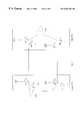
- FIG. 2illustrates a computer system 200 having a hub system 201 coupled to a processor unit 202 .
- the hub system 201is implemented within a display 203 and is fully integrated within the display 203 .
- Additional peripheralssuch as a keyboard 204 , a mouse 205 , a digital camera 206 and a pair of speakers 207 a and 207 b are each coupled to the hub system 201 .
- the hub system 201acts as a pass through port or routing system and routes information between each of the peripherals and the processor unit 202 .
- the processor unit 202 and the hub system 201are coupled together by two different cable assemblies 210 a and 210 b.
- one of the cable assemblies 210 ais used for transferring digital pixel data to the display 203 in a first direction; and, the other cable assembly 210 b is used for communicating serial digital data back and forth between the processor unit 202 and each of the other peripherals coupled to the hub system 201 .
- Each cable assemblyhas a limited number of wires, such that this configuration is preferable over the prior art system illustrated in FIG. 1 .
- cable assembly 210 amay be configured to transmit digital pixel data to display 203 using any one of several applicable transmission protocols such as TDMS (Transition Minimized Differential Sensing), LVDS (Low Voltage Differential Sensing), or analog RGB communications.
- Cable assembly 210 bmay be configured to transmit digital data using any applicable digital communications protocol such as the USB (Universal Serial Bus) standards.
- Digital pixel data intended to be displayed by display 203is received over the first cable assembly 210 a, retained, and properly processed for display by the display 203 .
- the serial digital data intended for any of the other peripheralsis received over the second cable assembly 210 b, passed through the hub system 201 , and routed to the proper peripheral. Accordingly, each of the other peripherals sends information to the processor unit 202 or receives information from the processor unit 202 through the hub system 201 over cable assembly 210 b; while the display 203 receives digital pixel data over cable assembly 210 a.
- cable assembly 210 aIn a computer system wherein TDMS communications are used for transferring digital pixel data, cable assembly 210 a will include four twisted wire differential pairs. Alternatively, in a computer system in which LVDS communications are used for transferring digital pixel data, cable assembly 210 a will include five twisted wire differential pairs. In TDMS communications, one twisted wire differential pair is used for each of the primary red, green and blue digital pixel data streams and the fourth twisted wire differential pair is used for transmitting a clock signal. Systems which use LVDS communications transmit digital pixel data over four dual wire pairs, with a fifth dual wire pair used for transmitting a clock signal.
- TMDS and LVDS communicationsrequire a horizontal video blanking period between the transmission of digital pixel data for each line in a display, and a vertical blanking period between the transmission of each frame to be displayed.
- FIG. 3further illustrates the communication of digital pixel data over cable assembly 210 a between processing unit 202 and display 203 in a computer system which utilizes TDMS communications.
- a transmitter 301is implemented within the processor 202 for transmitting digital pixel data from the processor 202 to the display 203 .
- a receiver 302is implemented within the display 203 having a hub system for receiving digital pixel data for display from the processor 202 .
- Cable assembly 210 ais comprised of four twisted wire pairs, with a first twisted wire pair 305 a used for transmitting red pixel data from the processor 202 to display 203 , a second twisted wire pair 305 b used for transmitting green pixel data from the processor 202 to display 203 , and a third twisted pair 305 c used for transferring blue pixel data from the processor 202 to display 203 .
- the fourth twisted wire pair 305 dis used for routing a clock signal from the processor 202 to the display 203 for synchronizing the digital pixel data at the receiver 302 .
- an enable signal DATA ENABLEis coupled to transmitter 301 . When the DATA ENABLE signal is active, digital pixel data is actively transmitted over twisted wire differential pairs 305 a - 305 c to display 203 .
- FIG. 4illustrates a timing diagram which shows waveforms for the forward transfer of digital pixel data to the display 203 .
- the DATA ENABLE signalwhen the DATA ENABLE signal is active, digital pixel data for a single line in the display is transferred to display 203 over twisted wire differential pairs 305 a - 305 c.
- the DATA ENABLE signalWhen the DATA ENABLE signal is inactive, no valid digital pixel data is transmitted over the twisted wire differential pairs 305 a - 305 c. Between lines this is known as the horizontal video blanking period. Between frames this is known as the vertical video blanking period.
- FIG. 4illustrates both the horizontal and vertical video blanking periods. As shown, the vertical blanking period is much longer than that horizontal video blanking period.
- a brief sampling of synchronization datais pulsed over all three twisted wire differential pairs 305 a - 305 c during the horizontal and vertical video blanking periods in order to resynchronize the three color channels (red, green and blue) before digital pixel data for a next line to be displayed or a first line in a next frame is transferred.
- the transmission of the synchronization datais only a small segment of the horizontal or vertical blanking period.
- no datais transferred over the three twisted wire differential pairs 305 a - 305 c.
- cable assembly 210 bwill also include a number of wires for transferring digital data back and forth between each of the peripherals coupled to the display with built-in hub system and the processor unit.
- the number of wiresis dependent upon the particular system configuration. For example, it is desirable to be able to transmit digital data from the digital camera to the processor, while also transmitting data from the mouse or keyboard and accordingly multiple wires are required.
- the processor unit 202further includes a receiver 310 , while the display 203 with hub system includes a transmitter 315 .
- the transmitter 315 of the display 203 with hub systemroutes digital information incoming from the other peripherals coupled to the display 203 to the receiver in the processor 202
- While the computer system illustrated in FIG. 3may reduce the overall number of cable assemblies coupled directly to the processor 202 , it is still undesirable because it still requires a large number of wires and two different cable assemblies. Accordingly, what is needed is a simpler system for linking the processor unit with the hub system without requiring multiple cabling assemblies which also reduces the number of wires coupled to the processor, thereby reducing costs and improving the ease of use of the system.
- Digital pixel datais transferred from a computer system to video display hardware in one direction using a known communications protocol such as TDMS or LVDS.
- TDMSTime Division Multiple Access
- LVDSLow-power Digital pixel data
- This inventiondescribes a method of sending digital data from any number of peripherals to a processor in a computer system in a reverse direction over a set of lines couple between the processor and a display. Transmission of video data over a set of lines coupled between the processor and the display typically requires horizontal and vertical video blanking periods during which special characters are used to resynchronize the forward transmission of a next line or a first line in a next frame of digital pixel data to a clock signal.
- some or all of the forward direction data pathscan be “turned around” in order to transmit digital data in a reverse direction during the horizontal and vertical video blanking periods.
- the beginning and end of the usable portion of the horizontal and vertical video blanking periodsmay be automatically programmed such that all of the lines may be used for reverse transmission of digital data, wherein the usable portion is predefined and all lines automatically switch back and forth from forward direction to reverse direction and back again at predefined times.
- one of the linesmay be used to mark the usable portion of the horizontal and verical video blanking periods, wherein all other lines are “turned around” and the one line continues to transmit data in a forward direction, thereby indicating the useable portion of the horizontal and vertical video blanking periods.
- a separate line carrying a clock signalmay be used to clock data in both directions of data transmission.
- FIG. 1illustrates a conventional computer system having a processor unit and a number of peripherals coupled to the processor;
- FIG. 2illustrates a conventional embodiment of a computer system having a hub system coupled to a processor unit which utilizes two uni-directional cable assemblies for communications between the processor unit and the hub system;
- FIG. 3illustrates a prior art system for transmitting digital pixel data in a forward direction over a first set of wires coupled between a processing unit and a display and receiving digital data in a second direction over a second set of wires coupled between the processing unit and the display;
- FIG. 4illustrates a timing diagram which shows waveforms for the conventional forward direction transfer of digital pixel data to a display
- FIG. 5illustrates a preferred embodiment of a computer system having a processor and display terminal coupled together with bi-directional data transfer over a single set of wires in accordance with the present invention
- FIGS. 6 a - 6 billustrate waveforms showing the transmission of digital data in a reverse direction in a preferred embodiment of the present invention
- FIG. 7illustrates an alternate embodiment for bi-directional data transfer over a single set of wires in accordance with the present invention.
- FIGS. 8 a - 8 cillustrate waveforms showing the transmission of digital data in a reverse direction in an alternate embodiment of the present invention.
- digital pixel data for each line in a video displayis transferred from the processor to the video display in a first direction over a series of wires or differential pairs whenever a data enable signal is active.
- digital pixel data for and corresponding control signals for a next line in the video displayare resynchronized. This is known as a horizontal video blanking period. During this horizontal video blanking period, no valid digital pixel data is transferred over the series of wires or differential pairs.
- the data enable signalis also inactive and digital pixel data and corresponding control signals for a first line in a new frame to be displayed are synchronized. This is known as the vertical video blanking period.
- the inventionallows for bidirectional data transfer over the series of wires or differential pairs coupled between between the processor and the video display with built-in hub system during the horizontal and vertical video blanking periods.
- red, green and blue digital pixel datais transferred over a plurality of wires in a first direction using a know digital communications protocol such as TDMS or LVDS.
- the digital pixel datais transferred from the processor to the display terminal whenever a data enable signal is active.
- digital datamay be serially transmitted in a reverse direction from the display terminal with hub system over all or some of the wires in the plurality. In this way, bidirectional data transfer is accomplished and the number of wires coupled between the processor and display terminal with hub system is reduced.
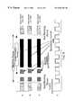
- FIG. 5illustrates a computer system which incorporates a preferred embodiment of the bidirectional data transfer system of the present invention.
- a processor 401includes a transmitter 406 , a receiver 410 , and a first transmit/receive circuit 420 which is coupled to both the transmitter 406 and the receiver 410 .
- a TDMS communications protocolis used to transfer digital pixel data from processor 401 to a video display terminal 402 Accordingly, the processor is coupled to a video display terminal 402 through four twisted wire pairs 405 a-d.
- the video display terminal 402is an active matrix flat panel display; however, it is understood that any other video display terminal may be used in alternate embodiments, so long as the communications between the processor 401 and the display terminal 402 are in a digital format.
- the four twisted wire pairs 405 a-dare preferably implemented within a single cable assembly.
- the display terminal 402includes a receiver 407 , a transmitter 415 , and a second transmit/receive circuit 430 coupled to both the receiver 407 and the transmitter 415 .
- the second transmit/receive circuit 430couples incoming digital pixel data to the receiver 407 , which receives the incoming digital pixel data and routes the data to row and column driver circuitry within the display terminal 402 .
- Row and column driver circuitryis well known in the art and is not an aspect of this invention. Accordingly, the display terminal 402 may embody any type of row and column driver circuitry known in the art for producing a displayed image on the display terminal 402 .
- the transmitter 415 in the display terminal 402receives incoming digital data from a number of peripherals which may be coupled to the display terminal 402 and transmits this digital data through the second transmit/receive circuit 430 to the processor unit 401 .
- peripheralsmay include a keyboard, a mouse, a digital camera, or a pair of audio speakers. It is understood that other peripherals may be coupled to the display terminal 402 .
- the display terminal of FIG. 5is similar to the display terminal illustrated in FIG. 2 .
- display terminal 402 shown in FIG. 5is coupled to the processor 401 through a single cable assembly having four twisted wire pairs 405 a-d. No additional wires or wire pairs are required to transmit digital data in a reverse direction.
- the computer system of FIG. 5is able to transfer digital pixel data from the processor 401 to the display terminal 402 in a forward direction, and is further able to transfer digital data from any of the peripherals coupled to the display terminal 402 to the processor 301 in a reverse direction over the four twisted wire pairs 405 a-d within a single cable assembly.
- the processorgenerates digital pixel data for display on the display terminal 402 and this digital pixel data is transferred in a forward direction from the processor 401 to the display terminal 402 over three of the four wire pairs 405 a, 405 b and 405 c whenever the data enable signal is active.
- the digital pixel datais transferred using the TDMS communications protocol.
- the data enable signalis inactive, no valid digital pixel data is transferred from the processor 401 to the display terminal 402 . This may occur during the horizontal video blanking period or the vertical video blanking period.
- the processorresynchronizes digital pixel data and the clock signal for a next line to be displayed on the display terminal or a first line in a next frame.
- the resynchronization processrequires only a fraction of the horizontal or vertical video blanking period.
- no valid datais transferred over wire pairs 405 a, 405 b, and 405 c while the data enable signal remains inactive. It is during this extra time period that digital data may be transferred back to the processor 401 from the display terminal 402 in a reverse direction using the present invention.
- the processor 401includes a transmitter 406 , a receiver 410 unit, and a first transmit/receive circuit 420 coupled to both the transmitter 406 and the receiver 410 .
- the display terminal 402also includes a receiver 407 , a transmitter 415 , and a second transmit/receive circuit 430 coupled to both the receiver 407 and the transmitter 415 .
- Four twisted wire pairs 405 a-dare coupled between the processor and the hub system of the display terminal 402 .
- the four wire pairsare implemented within a single cable assembly.
- One twisted pair 405 ais used for transmitting red digital pixel data and control signals from the processor 401 to the display terminal 402
- a second twisted pair 405 bused for transmitting green digital pixel data and control signals from the processor 401 to the display terminal 402
- a third twisted pair 405 cis used for transmitting blue digital pixel data and control signals from the processor 401 to the display terminal 402
- a fourth twisted pair 405 dis used for transmitting a differential clock signal from the processor 401 to the display terminal 402 .
- the red, green and blue digital pixel datais transferred from the processor to the display terminal whenever a data enable signal is active.
- the first and second twisted wire pairs 405 a and 405 bare used for transmitting digital data from any number of peripherals which may be coupled to the display terminal 402 to the processor 401 .
- the third twisted wire pairis preferably used to mark the beginning and ending of that portion of the horizontal or vertical video blanking period which may be used for bidirectional data transfer.
- all three linesmay use for bidirectional data transfer.
- the systemhas horizontal and vertical video blanking periods of known duration.
- Digital pixel datamay be transferred in a reverse direction from the peripherals to the processor during the useable portion of these video blanking periods and all lines may be programmed to automatically switch back and forth from forward to reverse direction and then back again at predetermined time intervals during the horizontal and vertical video blanking periods.
- FIGS. 6 a - 6 billustrate the transmission of digital data in a reverse direction in a first preferred embodiment of the present invention.
- digital datais transmitted in a reverse direction over the first and second twisted wire pairs from the display terminal 402 to the processor 401 , and the third twisted wire pair 405 c is used to track the usable portions of the horizontal and vertical video blanking periods which may be used for transmitting digital data in a reverse direction over lines 405 a and 405 b.
- the data enable signalis inactive, digital pixel data is not transmitted from the processor 402 . This occurs during the horizontal and vertical video blanking periods.
- a re-synchronization pulseis preferably transmitted over all three twisted wire pairs 405 a, 405 b and 405 c in order to forward synchronize the lines for the next transmission of digital pixel data.
- the re-synchronization pulseis only a fraction of the entire video blanking period whether the period is horizontal or vertical.
- the twisted wire pairs 405 a, 405 b and 405 cwill ordinarily remain inactive until digital pixel data for a next line or a first line in a next image to be displayed is transmitted. It is during this time that bidirectional data transfer is accomplished using the present invention.
- the first and second twisted wire pairs 405 a and 405 bare used for transmitting digital information from peripherals coupled to the display terminal 402 in a reverse direction to processor 401 .
- the processor 401immediately following the transmission of the forward direction re-synchronization pulses over all three twisted wire pairs 405 a, 405 b and 405 c, the processor 401 causes the first transmit/receive circuit 420 to reroute the first and second dual wire pairs 405 a and 405 b to the receiver 410 in processor 410 .
- the processor 401also transmits a start blanking pulse STARTBLANK over the third wire pair 405 .
- FIG. 6 bshows the transmission of STARTBLANK over the third dual wire pair 405 c.
- the start blanking pulse STARTBLANKcauses the second transmit/receive circuit 430 to reroute the first and second wire pairs 405 a and 405 b to the transmitter 415 in display 402 , thereby allowing digital data to be transmitted over these two dual wire pairs 405 a and 405 b.
- Digital datamay then be serially transmitted from the transmitter 415 of the display terminal 402 to the receiver 410 of the processor 401 via the first and second twisted wire pairs 405 a and 405 b.
- the display terminal 402begins transmitting data over the first and second twisted wire pairs 405 in a reverse direction.
- the display terminal 402will first transmit a synchronization pulse in the opposite direction in order to ensure synchronization at the receiver 410 in the processor 401 .
- the transmitter 415 in the display terminal 402then begins serially transmitting digital data in a reverse direction over the first and second twisted wires pairs 405 a and 405 b to the receiver 410 in the processor 401 .
- the digital datais routed from any one of several peripherals which may be coupled to the display terminal 402 .
- the processor 401transmits a signal indicating the end of the blanking period END BLANK over the third wire pair 405 c.
- the first transmit/receive circuit 420once again reroutes the first and second dual wire pairs 405 a and 405 b to the transmitter 406 in the processor 401
- the ENDBLANK signalinstructs the display terminal to stop transmitting data in the reverse direction and the second transmit/receive circuit 430 once again reroutes the first and second twisted wire pairs 405 a and 405 b to receiver 407 in the display terminal 402 .
- the display terminal 402switches into receive mode and prepares to receive the next transmission of digital pixel data over the first, second and third twisted wire pairs 405 a, 405 b and 405 c. Accordingly, the third twisted wire pair 405 c is used to signal when the blanking period begins and ends, and controls the transmission of data over the first and second twisted wire pairs 405 a and 405 b in the reverse direction.
- the transmitted clock signalprovides the necessary frequency information to transmit the data in the backwards direction.
- the backwards transmitted datahas its own re-synchronization pulse which sets the phase of the data in the same way that it is for the forward direction.
- the clock signal in the processor 401is used to control the receipt of digital data over the two signaling lines 405 a and 405 b in the reverse direction, as well as control the transmission of digital information over the third line 405 c in the forward direction.
- the display terminal 402may have its own clock signal generator and one of the lines 405 a or 405 b may be used for transmitting a clock signal from the display 402 to processor 401 in order to transmit digital data in a reverse direction at a different clock rate.
- digital data which is to be transferred in the reverse direction from the display terminal to the processoris preferably gated or buffered in a first-in-first-out memory until the horizontal or vertical video blanking periods occur. This allows the digital data to be accepted at any time from the peripherals and stored in the display 402 until it can be transmitted when the reverse channels are available.
- FIGS. 5 and 6have described the preferred embodiment with reference to a system which uses TDMS communications and four twisted wire differential pairs, it is understood the embodiment is nearly identical in a system using LVDS and five twisted wire pairs. In such an embodiment, these wires pairs are then available for the reverse transmission with the fourth wire pair used for signaling those portions of the horizontal and vertical video blanking periods which may be used. The fifth wire pair would be used for transmitting a clock signal.
- FIG. 7illustrates another preferred embodiment for implementing the present invention for convenience.
- FIG. 7illustrates the implementation over a single twisted wire pair, and it is understood that in a system utilizing TDMS communications all four twisted wire differential pairs may include the design set forth in FIG. 7 or in a system utilizing LVDS communications all five twisted wire differential pairs may include the design set forth in FIG. 7 .
- a twisted wire pair 700is coupled between the processor 701 and the display with built in hub system 702 for bidirectional transfer of information.
- Digital pixel datais transferred in a forward direction from the processor 701 to the display with built in hub system 702 whenever a data enable signal is active.
- transistors X 1 and X 2 in the processor 701are activated as digital pixel data is applied to their gates, while transistors XS 3 and XS 4 remain inactive.
- Transistors XS 1 and XS 2 in the displayare also activated, while transistors XR 1 and XR 2 are inactive.
- the transistors X 1 and X 2 in the processor 701are activated, the voltages at the inputs to the amplifier AMP 1 in the display with built in hub system 702 are modulated and the output from the amplifier AMP 1 reflects the changes in digital pixel data applied to the gates of transistors X 1 and X 2 .
- the transistors X 1 and X 2 in the processor 701are turned off and the transistors XS 3 and XS 4 in the processor are turned on.
- the transistors XS 1 and XS 2are each turned off, while the transistors XR 1 and XR 2 are activated as digital pixel data received from peripherals coupled to the hub system of the display 702 is applied to their gates.
- the transistors XR 1 and XR 2 in the processor 701are activated with digital pixel data
- the voltages at the inputs to the amplifier AMP 2 in the processor 702are modulated and the output from the amplifier AMP 2 reflects the changes in digital pixel data applied to the gates of transistors XR 1 and XR 2 .
- Digital datais thus transmitted in a reverse direction over the twisted wire differential pair until the end of the horizontal or vertical video blanking period. It is understood, that alternate embodiments may exist for transferring digital data in a reverse direction.
- FIGS. 8 a- 8 cillustrate a preferred embodiment wherein digital data may be transferred in a reverse direction from the transmitter 415 in the display 402 to the receiver 410 in the processor 401 .
- the start and stop times of the switchingare predetermined and last for a predetermined number of clock cycles.
- the structure of this embodimentmay be identical to that shown in FIG. 5 or FIG. 7, except that in this particular embodiment, all three data lines 405 a-c in a TDMS system (or all four data lines in a LVDS system) can switch orientation for a predetermined length of time.
- the receiver 407 in the display 402will include a counter which is coupled to the incoming clock signal from the dedicated clock line (line 405 d in FIG. 4 ). This counter keeps track of the number of clock pulses which are transmitted over the dedicated clock line.
- the horizontal and video blanking periodsare each of a known duration or length of time (which is measured in clock pulses) and transfer of digital data in a reverse direction is controlled by the clock signal.
- the processor 401reroutes all three of the dual wire pairs 405 a-c to the receiver 410 .
- the forward synchronization pulseis then received at the receiver 407 in display 402 .
- the display 402reroutes all three twisted wire pairs 405 a-c to the transmitter 415 and the reverse transmission of digital data can ensue.
- a reverse synchronization pulsewill be translated over each line to ensure synchronization of received data with the clock in the processor 401 .
- the horizontal and vertical video blanking periodslast for a predetermined number of clock periods and the display 402 includes a counter for tracking the number of clock signals received.
- FIG. 8dshows the clock pulse which is transmitted from the processor 401 to the display 402 over a separate line.
- the transmitter 415 in the display 402stops transmitting digital data in a reverse direction and the display 402 reroutes the three signal lines 405 a-c to the receiver 407 in display 402 .
- FIGS. 8 a-dillustrate that on the rising edge of the last clock pulse in transmitted during the video blanking period (horizontal or vertial) the data transmission in the reverse direction stops over all three data lines.
- the processorthen automatically reroutes the data lines 405 a-c to the transmitter 406 in the processor 401 , and the processor 402 will begin to transmit digital pixel data for a next line, or a first line in a next frame, to the display 402 .
- the transmission rate and the number of blanking periods per secondallow for most applications.
- the data rate for an XGA (1024 ⁇ 768) display at 24 bits per pixel (8 bits per red, green and blue subpixels) and 60 Hz refreshis 142 MBytes per second. Accordingly, if the horizontal and vertical blanking periods are used for transmitting digital data in the reverse direction (with approximately 10% of the blanking period used for overhead to switch data flow direction) then a reverse data rate of 21 Mbytes per second can be achieved.
Landscapes
- Engineering & Computer Science (AREA)
- Multimedia (AREA)
- Signal Processing (AREA)
- Theoretical Computer Science (AREA)
- Physics & Mathematics (AREA)
- General Physics & Mathematics (AREA)
- Power Engineering (AREA)
- Computer Hardware Design (AREA)
- Human Computer Interaction (AREA)
- General Engineering & Computer Science (AREA)
- Controls And Circuits For Display Device (AREA)
- Control Of Indicators Other Than Cathode Ray Tubes (AREA)
- Television Systems (AREA)
- Two-Way Televisions, Distribution Of Moving Picture Or The Like (AREA)
- Digital Computer Display Output (AREA)
- Time-Division Multiplex Systems (AREA)
Abstract
Description
Claims (23)
Priority Applications (8)
| Application Number | Priority Date | Filing Date | Title |
|---|---|---|---|
| US09/392,229US6564269B1 (en) | 1998-09-10 | 1999-09-08 | Bi-directional data transfer using the video blanking period in a digital data stream |
| PCT/US1999/020839WO2000014626A1 (en) | 1998-09-10 | 1999-09-09 | Bi-directional data transfer using the video blanking period in a digital data stream |
| AU60340/99AAU6034099A (en) | 1998-09-10 | 1999-09-09 | Bi-directional data transfer using the video blanking period in a digital data stream |
| CA002343122ACA2343122A1 (en) | 1998-09-10 | 1999-09-09 | Bi-directional data transfer using the video blanking period in a digital data stream |
| JP2000569306AJP5053484B2 (en) | 1998-09-10 | 1999-09-09 | Bidirectional data transmission using video blanking period of digital data stream |
| KR1020017003046AKR100655843B1 (en) | 1998-09-10 | 1999-09-09 | Bidirectional data transmission using video blanking period of digital data stream |
| JP2010165603AJP5438616B2 (en) | 1998-09-10 | 2010-07-23 | Bidirectional data transmission using video blanking period of digital data stream |
| JP2013229919AJP5738963B2 (en) | 1998-09-10 | 2013-11-06 | Bidirectional data transmission using video blanking period of digital data stream |
Applications Claiming Priority (2)
| Application Number | Priority Date | Filing Date | Title |
|---|---|---|---|
| US9982198P | 1998-09-10 | 1998-09-10 | |
| US09/392,229US6564269B1 (en) | 1998-09-10 | 1999-09-08 | Bi-directional data transfer using the video blanking period in a digital data stream |
Publications (1)
| Publication Number | Publication Date |
|---|---|
| US6564269B1true US6564269B1 (en) | 2003-05-13 |
Family
ID=26796511
Family Applications (1)
| Application Number | Title | Priority Date | Filing Date |
|---|---|---|---|
| US09/392,229Expired - LifetimeUS6564269B1 (en) | 1998-09-10 | 1999-09-08 | Bi-directional data transfer using the video blanking period in a digital data stream |
Country Status (6)
| Country | Link |
|---|---|
| US (1) | US6564269B1 (en) |
| JP (3) | JP5053484B2 (en) |
| KR (1) | KR100655843B1 (en) |
| AU (1) | AU6034099A (en) |
| CA (1) | CA2343122A1 (en) |
| WO (1) | WO2000014626A1 (en) |
Cited By (32)
| Publication number | Priority date | Publication date | Assignee | Title |
|---|---|---|---|---|
| US20020056137A1 (en)* | 1994-01-05 | 2002-05-09 | Cybex Computer Products Corporation | Twisted pair communications line system |
| US20020149545A1 (en)* | 1999-11-15 | 2002-10-17 | Ryotaro Hanayama | Head mounted display system |
| US20030071799A1 (en)* | 2001-10-17 | 2003-04-17 | Myers Robert L. | System for bi-directional video signal transmission |
| US20040080523A1 (en)* | 2002-10-24 | 2004-04-29 | Myers Robert L. | System and method for transferring data through a video interface |
| US20040217948A1 (en)* | 2003-04-30 | 2004-11-04 | Sony Corporation | Method and system for wireless digital video presentation |
| US6831924B1 (en)* | 2000-07-20 | 2004-12-14 | Silicon Graphics, Inc. | Variable mode bi-directional and uni-directional computer communication system |
| US20050025260A1 (en)* | 2003-07-31 | 2005-02-03 | Analog Devices, Inc. | Structures and methods for capturing data from data bit streams |
| WO2005029857A1 (en)* | 2003-09-22 | 2005-03-31 | Inova Semiconductors Gmbh | System and method for lossless reduction of bandwidth of a data stream transmitted via a digital multimedia link |
| US20050136990A1 (en)* | 2003-12-22 | 2005-06-23 | Sony Corporation | Method and system for wireless digital multimedia presentation |
| US20060179201A1 (en)* | 2003-09-22 | 2006-08-10 | Inova Semiconductors Gmbh | Reducing bandwidth of a data stream transmitted via a digital multimedia link without losing data |
| US7230650B2 (en)* | 2001-02-01 | 2007-06-12 | Sony Corporation | Data transmission method, data receiving method, video data transmission apparatus and video data receiving apparatus |
| US20080068323A1 (en)* | 2006-09-19 | 2008-03-20 | Novatek Microelectronics Corp. | Integrated display panel |
| US20080086749A1 (en)* | 2006-10-06 | 2008-04-10 | Netanel Goldberg | Device, method and system of wireless communication of user input to a video source |
| US7558326B1 (en)* | 2001-09-12 | 2009-07-07 | Silicon Image, Inc. | Method and apparatus for sending auxiliary data on a TMDS-like link |
| US7643018B1 (en) | 1994-01-05 | 2010-01-05 | Avocent Corporation | Twisted pair communications line system |
| US7792152B1 (en) | 2004-06-08 | 2010-09-07 | Owlink Technology, Inc. | Scheme for transmitting video and audio data of variable formats over a serial link of a fixed data rate |
| US20120151537A1 (en)* | 2010-12-14 | 2012-06-14 | Samsung Electronics Co., Ltd. | Method and system for asynchronous and isochronous data transmission in a high speed video network |
| US20130050216A1 (en)* | 2011-08-31 | 2013-02-28 | Colin Whitby-Strevens | Methods and apparatus for low power audio visual interface interoperability |
| US8995596B1 (en) | 2012-02-08 | 2015-03-31 | Altera Corporation | Techniques for calibrating a clock signal |
| US20160028534A1 (en)* | 2013-10-03 | 2016-01-28 | Qualcomm Incorporated | Multi-lane n-factorial (n!) and other multi-wire communication systems |
| US20160125840A1 (en)* | 2014-11-05 | 2016-05-05 | Silicon Works Co., Ltd. | Display device |
| EP3163564A1 (en)* | 2015-10-30 | 2017-05-03 | LG Display Co., Ltd. | Organic light emitting diode display device |
| US9673961B2 (en) | 2014-04-10 | 2017-06-06 | Qualcomm Incorporated | Multi-lane N-factorial (N!) and other multi-wire communication systems |
| US9673968B2 (en) | 2013-03-20 | 2017-06-06 | Qualcomm Incorporated | Multi-wire open-drain link with data symbol transition based clocking |
| US9673969B2 (en) | 2013-03-07 | 2017-06-06 | Qualcomm Incorporated | Transcoding method for multi-wire signaling that embeds clock information in transition of signal state |
| US20170193877A1 (en)* | 2015-12-31 | 2017-07-06 | Lg Display Co., Ltd. | Organic Light Emitting Diode Display Device |
| US9755818B2 (en) | 2013-10-03 | 2017-09-05 | Qualcomm Incorporated | Method to enhance MIPI D-PHY link rate with minimal PHY changes and no protocol changes |
| US20170315652A1 (en)* | 2016-04-27 | 2017-11-02 | Qualcomm Incorporated | Variable rate display interfaces |
| US9852103B2 (en) | 2014-04-14 | 2017-12-26 | Lattice Semiconductor Corporation | Bidirectional transmission of USB data using audio/video data channel |
| US20180145822A1 (en)* | 2015-06-15 | 2018-05-24 | Sony Corporation | Transmission device, reception device, communication system, signal transmission method, signal reception method, and communication method |
| CN110399113A (en)* | 2018-04-24 | 2019-11-01 | 京东方科技集团股份有限公司 | Data transmission method, device and display device |
| CN117560460A (en)* | 2024-01-12 | 2024-02-13 | 杭州海康威视数字技术股份有限公司 | Conversion circuit for video analog signal transmission |
Families Citing this family (15)
| Publication number | Priority date | Publication date | Assignee | Title |
|---|---|---|---|---|
| WO2002009443A1 (en) | 2000-07-21 | 2002-01-31 | Matsushita Electric Industrial Co., Ltd. | Signal transmitting device and signal receiving device |
| US7327381B2 (en) | 2000-09-25 | 2008-02-05 | Matsushita Electric Industrial Co., Ltd. | Signal transmission system, signal transmitter, and signal receiver |
| JP4008688B2 (en) | 2000-10-12 | 2007-11-14 | 松下電器産業株式会社 | Signal transmitting apparatus and signal receiving apparatus |
| JP4320117B2 (en)* | 2000-11-22 | 2009-08-26 | 富士フイルム株式会社 | Image display method and image display apparatus |
| CN1227908C (en) | 2000-12-18 | 2005-11-16 | 松下电器产业株式会社 | Encryption transmission system |
| EP1233626A1 (en)* | 2001-01-24 | 2002-08-21 | Broadcom Corporation | Digital video interface supporting transport of audio and auxiliary data |
| US7356051B2 (en) | 2001-01-24 | 2008-04-08 | Broadcom Corporation | Digital visual interface with audio and auxiliary data cross reference to related applications |
| US20020097869A1 (en)* | 2001-01-24 | 2002-07-25 | Christopher Pasqualino | System and method for increased data capacity of a digital video link |
| JP3903721B2 (en) | 2001-03-12 | 2007-04-11 | ソニー株式会社 | Information transmitting apparatus and method, information receiving apparatus and method, information transmitting / receiving system and method, recording medium, and program |
| EP1357752A4 (en)* | 2001-06-25 | 2010-06-02 | Panasonic Corp | VIDEO TRANSMITTER SYSTEM WITH BASE BAND |
| US7019791B2 (en) | 2001-11-09 | 2006-03-28 | Hitachi, Ltd. | Video processing device |
| KR101459772B1 (en)* | 2007-09-04 | 2014-11-13 | 한국전자통신연구원 | Apparatus for tranceiving point to point moving signal recepting high channel using hotrizontal blanking interval and method for excuting the apparatus |
| US8941592B2 (en)* | 2010-09-24 | 2015-01-27 | Intel Corporation | Techniques to control display activity |
| JP6039707B2 (en)* | 2015-01-19 | 2016-12-07 | 日立マクセル株式会社 | Video signal processing apparatus and method |
| JP6809079B2 (en)* | 2016-09-22 | 2021-01-06 | 三菱電機株式会社 | Image display device |
Citations (10)
| Publication number | Priority date | Publication date | Assignee | Title |
|---|---|---|---|---|
| US4414626A (en)* | 1977-10-12 | 1983-11-08 | Tokyo Shibaura Denki Kabushiki Kaisha | Input/output control system and methods |
| US5097410A (en)* | 1988-12-30 | 1992-03-17 | International Business Machines Corporation | Multimode data system for transferring control and data information in an i/o subsystem |
| WO1993006587A1 (en) | 1991-09-20 | 1993-04-01 | Icl Personal Systems Oy | A method for controlling a display device in a display system, and a display system and a display device |
| US5457473A (en) | 1992-02-20 | 1995-10-10 | Hitachi, Ltd. | Image display apparatus |
| EP0692760A2 (en) | 1994-07-15 | 1996-01-17 | International Business Machines Corporation | Data processing apparatus |
| US5675813A (en) | 1995-10-26 | 1997-10-07 | Microsoft Corporation | System and method for power control in a universal serial bus |
| JPH10116139A (en) | 1996-05-07 | 1998-05-06 | Samsung Electron Co Ltd | Display device and power supply control method thereof |
| US5781028A (en) | 1996-06-21 | 1998-07-14 | Microsoft Corporation | System and method for a switched data bus termination |
| US5796269A (en)* | 1996-04-09 | 1998-08-18 | Xilinx, Inc. | Composable memory array for a programmable logic device and method for implementing same |
| US5954813A (en)* | 1994-11-10 | 1999-09-21 | Motorola, Inc. | Data processor with transparent operation during a background mode and method therefor |
Family Cites Families (10)
| Publication number | Priority date | Publication date | Assignee | Title |
|---|---|---|---|---|
| JPH01276987A (en)* | 1988-04-28 | 1989-11-07 | Fuji Facom Corp | Time division multiplexing transmission system |
| JPH0535242A (en)* | 1991-07-31 | 1993-02-12 | Fujitsu Kiden Ltd | Image data transmission system |
| JP3396889B2 (en)* | 1991-11-26 | 2003-04-14 | ミノルタ株式会社 | Printer |
| JPH076571A (en)* | 1993-06-21 | 1995-01-10 | Mitsubishi Electric Corp | Recording / playback device with transmission function |
| JPH08186753A (en)* | 1994-12-28 | 1996-07-16 | Hitachi Ltd | Imaging device |
| JPH08221046A (en)* | 1995-02-17 | 1996-08-30 | Nec Eng Ltd | Bi-directional crt interface circuit |
| JPH0954569A (en)* | 1995-08-15 | 1997-02-25 | Toshiba Corp | Image display system and image display method |
| EP0778517A3 (en)* | 1995-11-27 | 1998-02-11 | Texas Instruments Incorporated | Improvements in or relating to the encoding of an image control signal |
| JPH10105298A (en)* | 1996-09-30 | 1998-04-24 | Canon Inc | Switching device |
| JPH10233955A (en)* | 1997-02-21 | 1998-09-02 | Canon Inc | Imaging device |
- 1999
- 1999-09-08USUS09/392,229patent/US6564269B1/ennot_activeExpired - Lifetime
- 1999-09-09AUAU60340/99Apatent/AU6034099A/ennot_activeAbandoned
- 1999-09-09JPJP2000569306Apatent/JP5053484B2/ennot_activeExpired - Lifetime
- 1999-09-09KRKR1020017003046Apatent/KR100655843B1/ennot_activeExpired - Lifetime
- 1999-09-09WOPCT/US1999/020839patent/WO2000014626A1/enactiveIP Right Grant
- 1999-09-09CACA002343122Apatent/CA2343122A1/ennot_activeAbandoned
- 2010
- 2010-07-23JPJP2010165603Apatent/JP5438616B2/ennot_activeExpired - Lifetime
- 2013
- 2013-11-06JPJP2013229919Apatent/JP5738963B2/ennot_activeExpired - Lifetime
Patent Citations (10)
| Publication number | Priority date | Publication date | Assignee | Title |
|---|---|---|---|---|
| US4414626A (en)* | 1977-10-12 | 1983-11-08 | Tokyo Shibaura Denki Kabushiki Kaisha | Input/output control system and methods |
| US5097410A (en)* | 1988-12-30 | 1992-03-17 | International Business Machines Corporation | Multimode data system for transferring control and data information in an i/o subsystem |
| WO1993006587A1 (en) | 1991-09-20 | 1993-04-01 | Icl Personal Systems Oy | A method for controlling a display device in a display system, and a display system and a display device |
| US5457473A (en) | 1992-02-20 | 1995-10-10 | Hitachi, Ltd. | Image display apparatus |
| EP0692760A2 (en) | 1994-07-15 | 1996-01-17 | International Business Machines Corporation | Data processing apparatus |
| US5954813A (en)* | 1994-11-10 | 1999-09-21 | Motorola, Inc. | Data processor with transparent operation during a background mode and method therefor |
| US5675813A (en) | 1995-10-26 | 1997-10-07 | Microsoft Corporation | System and method for power control in a universal serial bus |
| US5796269A (en)* | 1996-04-09 | 1998-08-18 | Xilinx, Inc. | Composable memory array for a programmable logic device and method for implementing same |
| JPH10116139A (en) | 1996-05-07 | 1998-05-06 | Samsung Electron Co Ltd | Display device and power supply control method thereof |
| US5781028A (en) | 1996-06-21 | 1998-07-14 | Microsoft Corporation | System and method for a switched data bus termination |
Cited By (55)
| Publication number | Priority date | Publication date | Assignee | Title |
|---|---|---|---|---|
| US7643018B1 (en) | 1994-01-05 | 2010-01-05 | Avocent Corporation | Twisted pair communications line system |
| US7206348B2 (en)* | 1994-01-05 | 2007-04-17 | Avocent Corporation | Twisted pair communications line system |
| US20020056137A1 (en)* | 1994-01-05 | 2002-05-09 | Cybex Computer Products Corporation | Twisted pair communications line system |
| US20020149545A1 (en)* | 1999-11-15 | 2002-10-17 | Ryotaro Hanayama | Head mounted display system |
| US6831924B1 (en)* | 2000-07-20 | 2004-12-14 | Silicon Graphics, Inc. | Variable mode bi-directional and uni-directional computer communication system |
| US7230650B2 (en)* | 2001-02-01 | 2007-06-12 | Sony Corporation | Data transmission method, data receiving method, video data transmission apparatus and video data receiving apparatus |
| US7558326B1 (en)* | 2001-09-12 | 2009-07-07 | Silicon Image, Inc. | Method and apparatus for sending auxiliary data on a TMDS-like link |
| US6914597B2 (en)* | 2001-10-17 | 2005-07-05 | Hewlett-Packard Development Company, L.P. | System for bi-directional video signal transmission |
| US20030071799A1 (en)* | 2001-10-17 | 2003-04-17 | Myers Robert L. | System for bi-directional video signal transmission |
| US6989827B2 (en)* | 2002-10-24 | 2006-01-24 | Hewlett-Packard Development Company, Lp. | System and method for transferring data through a video interface |
| US20040080523A1 (en)* | 2002-10-24 | 2004-04-29 | Myers Robert L. | System and method for transferring data through a video interface |
| US7965837B2 (en) | 2003-04-30 | 2011-06-21 | Sony Corporation | Method and system for wireless digital video presentation |
| US20040217948A1 (en)* | 2003-04-30 | 2004-11-04 | Sony Corporation | Method and system for wireless digital video presentation |
| US20050025260A1 (en)* | 2003-07-31 | 2005-02-03 | Analog Devices, Inc. | Structures and methods for capturing data from data bit streams |
| US7359458B2 (en) | 2003-07-31 | 2008-04-15 | Analog Devices, Inc. | Structures and methods for capturing data from data bit streams |
| US20060179201A1 (en)* | 2003-09-22 | 2006-08-10 | Inova Semiconductors Gmbh | Reducing bandwidth of a data stream transmitted via a digital multimedia link without losing data |
| WO2005029857A1 (en)* | 2003-09-22 | 2005-03-31 | Inova Semiconductors Gmbh | System and method for lossless reduction of bandwidth of a data stream transmitted via a digital multimedia link |
| US8000350B2 (en) | 2003-09-22 | 2011-08-16 | Inova Semiconductors Gmbh | Reducing bandwidth of a data stream transmitted via a digital multimedia link without losing data |
| US7562379B2 (en) | 2003-12-22 | 2009-07-14 | Sony Corporation | Method and system for wireless digital multimedia presentation |
| US20090235304A1 (en)* | 2003-12-22 | 2009-09-17 | Sony Corporation | Method and system for wireless digital multimedia presentation |
| US20050136990A1 (en)* | 2003-12-22 | 2005-06-23 | Sony Corporation | Method and system for wireless digital multimedia presentation |
| US7792152B1 (en) | 2004-06-08 | 2010-09-07 | Owlink Technology, Inc. | Scheme for transmitting video and audio data of variable formats over a serial link of a fixed data rate |
| US20080068323A1 (en)* | 2006-09-19 | 2008-03-20 | Novatek Microelectronics Corp. | Integrated display panel |
| US20080086749A1 (en)* | 2006-10-06 | 2008-04-10 | Netanel Goldberg | Device, method and system of wireless communication of user input to a video source |
| US20120151537A1 (en)* | 2010-12-14 | 2012-06-14 | Samsung Electronics Co., Ltd. | Method and system for asynchronous and isochronous data transmission in a high speed video network |
| US8831161B2 (en)* | 2011-08-31 | 2014-09-09 | Apple Inc. | Methods and apparatus for low power audio visual interface interoperability |
| US20130050216A1 (en)* | 2011-08-31 | 2013-02-28 | Colin Whitby-Strevens | Methods and apparatus for low power audio visual interface interoperability |
| US8995596B1 (en) | 2012-02-08 | 2015-03-31 | Altera Corporation | Techniques for calibrating a clock signal |
| US9673969B2 (en) | 2013-03-07 | 2017-06-06 | Qualcomm Incorporated | Transcoding method for multi-wire signaling that embeds clock information in transition of signal state |
| US9673968B2 (en) | 2013-03-20 | 2017-06-06 | Qualcomm Incorporated | Multi-wire open-drain link with data symbol transition based clocking |
| US9853806B2 (en) | 2013-10-03 | 2017-12-26 | Qualcomm Incorporated | Method to enhance MIPI D-PHY link rate with minimal PHY changes and no protocol changes |
| US20160028534A1 (en)* | 2013-10-03 | 2016-01-28 | Qualcomm Incorporated | Multi-lane n-factorial (n!) and other multi-wire communication systems |
| US9755818B2 (en) | 2013-10-03 | 2017-09-05 | Qualcomm Incorporated | Method to enhance MIPI D-PHY link rate with minimal PHY changes and no protocol changes |
| US9735948B2 (en)* | 2013-10-03 | 2017-08-15 | Qualcomm Incorporated | Multi-lane N-factorial (N!) and other multi-wire communication systems |
| US9673961B2 (en) | 2014-04-10 | 2017-06-06 | Qualcomm Incorporated | Multi-lane N-factorial (N!) and other multi-wire communication systems |
| US9852103B2 (en) | 2014-04-14 | 2017-12-26 | Lattice Semiconductor Corporation | Bidirectional transmission of USB data using audio/video data channel |
| US20160125840A1 (en)* | 2014-11-05 | 2016-05-05 | Silicon Works Co., Ltd. | Display device |
| US10380971B2 (en)* | 2014-11-05 | 2019-08-13 | Silicon Works Co., Ltd. | Display device |
| US10944536B2 (en)* | 2015-06-15 | 2021-03-09 | Sony Corporation | Transmission device, reception device, communication system, signal transmission method, signal reception method, and communication method |
| TWI705666B (en)* | 2015-06-15 | 2020-09-21 | 日商新力股份有限公司 | Transmission device, receiving device, communication system |
| US20200127805A1 (en)* | 2015-06-15 | 2020-04-23 | Sony Corporation | Transmission device, reception device, communication system, signal transmission method, signal reception method, and communication method |
| US10419200B2 (en)* | 2015-06-15 | 2019-09-17 | Sony Corporation | Transmission device, reception device, communication system, signal transmission method, signal reception method, and communication method |
| US20180145822A1 (en)* | 2015-06-15 | 2018-05-24 | Sony Corporation | Transmission device, reception device, communication system, signal transmission method, signal reception method, and communication method |
| CN107045853A (en)* | 2015-10-30 | 2017-08-15 | 乐金显示有限公司 | Organic LED display device |
| EP3163564A1 (en)* | 2015-10-30 | 2017-05-03 | LG Display Co., Ltd. | Organic light emitting diode display device |
| US10276093B2 (en) | 2015-10-30 | 2019-04-30 | Lg Display Co., Ltd. | Organic light emitting diode display device using vertical synchronization signals with different phase |
| US10013906B2 (en)* | 2015-12-31 | 2018-07-03 | Lg Display Co., Ltd. | Organic light emitting diode display device |
| CN106935175A (en)* | 2015-12-31 | 2017-07-07 | 乐金显示有限公司 | Organic LED display device |
| US20170193877A1 (en)* | 2015-12-31 | 2017-07-06 | Lg Display Co., Ltd. | Organic Light Emitting Diode Display Device |
| US20170315652A1 (en)* | 2016-04-27 | 2017-11-02 | Qualcomm Incorporated | Variable rate display interfaces |
| US10698522B2 (en)* | 2016-04-27 | 2020-06-30 | Qualcomm Incorporated | Variable rate display interfaces |
| CN110399113A (en)* | 2018-04-24 | 2019-11-01 | 京东方科技集团股份有限公司 | Data transmission method, device and display device |
| US11257439B2 (en) | 2018-04-24 | 2022-02-22 | Beijing Boe Display Technology Co., Ltd. | Data transmission method and device, display screen, and display device |
| CN117560460A (en)* | 2024-01-12 | 2024-02-13 | 杭州海康威视数字技术股份有限公司 | Conversion circuit for video analog signal transmission |
| CN117560460B (en)* | 2024-01-12 | 2024-04-09 | 杭州海康威视数字技术股份有限公司 | Conversion circuit for video analog signal transmission |
Also Published As
| Publication number | Publication date |
|---|---|
| CA2343122A1 (en) | 2000-03-16 |
| JP5053484B2 (en) | 2012-10-17 |
| JP5438616B2 (en) | 2014-03-12 |
| AU6034099A (en) | 2000-03-27 |
| WO2000014626A8 (en) | 2000-06-08 |
| KR100655843B1 (en) | 2006-12-12 |
| KR20010086391A (en) | 2001-09-10 |
| WO2000014626A1 (en) | 2000-03-16 |
| JP2002524949A (en) | 2002-08-06 |
| JP2014064298A (en) | 2014-04-10 |
| JP2010288298A (en) | 2010-12-24 |
| JP5738963B2 (en) | 2015-06-24 |
Similar Documents
| Publication | Publication Date | Title |
|---|---|---|
| US6564269B1 (en) | Bi-directional data transfer using the video blanking period in a digital data stream | |
| US8463961B2 (en) | Video switch | |
| US6963968B2 (en) | Signal transmission device and method | |
| US6693895B1 (en) | Multiple synchronous data stream format for an optical data link | |
| JP3352600B2 (en) | Display device | |
| EP0424743A2 (en) | Audio-video data interface for a high speed communication link in a video-graphics display window environment | |
| US20020049879A1 (en) | Cable and connection with integrated DVI and IEEE 1394 capabilities | |
| US20050165994A1 (en) | Signal transmission over a wire pair | |
| US11936927B2 (en) | Transmission control system of multi-media signal, transmitter control circuit and receiver control circuit | |
| US8332518B2 (en) | Bidirectional communication protocol between a serializer and a deserializer | |
| EP0778517A2 (en) | Improvements in or relating to the encoding of an image control signal | |
| US7062596B2 (en) | Self-synchronizing half duplex matrix switch | |
| JPH02127688A (en) | Control system for cathode-ray tube display device | |
| US6754240B1 (en) | Format for an optical data link | |
| JPH08298532A (en) | Data transmission system and signal selection connection device | |
| CA1256553A (en) | Digital transmission system | |
| JPH01276987A (en) | Time division multiplexing transmission system | |
| KR20010061844A (en) | Bidirectional system for transferring signal in liquid crystal display | |
| WO1993022759A1 (en) | Computer display system | |
| JPH1174856A (en) | Data transfer system | |
| GB2380889A (en) | Digital video switching | |
| JPH02136000A (en) | Data transfer system |
Legal Events
| Date | Code | Title | Description |
|---|---|---|---|
| AS | Assignment | Owner name:SILICON IMAGE, INC, CALIFORNIA Free format text:ASSIGNMENT OF ASSIGNORS INTEREST;ASSIGNOR:MARTIN, RUSSEL A.;REEL/FRAME:010401/0560 Effective date:19991026 | |
| STCF | Information on status: patent grant | Free format text:PATENTED CASE | |
| FEPP | Fee payment procedure | Free format text:PAYOR NUMBER ASSIGNED (ORIGINAL EVENT CODE: ASPN); ENTITY STATUS OF PATENT OWNER: LARGE ENTITY | |
| FPAY | Fee payment | Year of fee payment:4 | |
| FEPP | Fee payment procedure | Free format text:PAT HOLDER NO LONGER CLAIMS SMALL ENTITY STATUS, ENTITY STATUS SET TO UNDISCOUNTED (ORIGINAL EVENT CODE: STOL); ENTITY STATUS OF PATENT OWNER: LARGE ENTITY | |
| FPAY | Fee payment | Year of fee payment:8 | |
| FPAY | Fee payment | Year of fee payment:12 | |
| AS | Assignment | Owner name:JEFFERIES FINANCE LLC, NEW YORK Free format text:SECURITY INTEREST;ASSIGNORS:LATTICE SEMICONDUCTOR CORPORATION;SIBEAM, INC.;SILICON IMAGE, INC.;AND OTHERS;REEL/FRAME:035220/0226 Effective date:20150310 | |
| AS | Assignment | Owner name:LATTICE SEMICONDUCTOR CORPORATION, OREGON Free format text:MERGER;ASSIGNOR:SILICON IMAGE, INC.;REEL/FRAME:036419/0792 Effective date:20150513 | |
| AS | Assignment | Owner name:DVDO, INC., OREGON Free format text:RELEASE BY SECURED PARTY;ASSIGNOR:JEFFERIES FINANCE LLC;REEL/FRAME:049827/0326 Effective date:20190517 Owner name:SILICON IMAGE, INC., OREGON Free format text:RELEASE BY SECURED PARTY;ASSIGNOR:JEFFERIES FINANCE LLC;REEL/FRAME:049827/0326 Effective date:20190517 Owner name:LATTICE SEMICONDUCTOR CORPORATION, OREGON Free format text:RELEASE BY SECURED PARTY;ASSIGNOR:JEFFERIES FINANCE LLC;REEL/FRAME:049827/0326 Effective date:20190517 Owner name:SIBEAM, INC., OREGON Free format text:RELEASE BY SECURED PARTY;ASSIGNOR:JEFFERIES FINANCE LLC;REEL/FRAME:049827/0326 Effective date:20190517 | |
| AS | Assignment | Owner name:WELLS FARGO BANK, NATIONAL ASSOCIATION, AS ADMINIS Free format text:SECURITY INTEREST;ASSIGNOR:LATTICE SEMICONDUCTOR CORPORATION;REEL/FRAME:049795/0481 Effective date:20190718 Owner name:WELLS FARGO BANK, NATIONAL ASSOCIATION, AS ADMINISTRATIVE AGENT, COLORADO Free format text:SECURITY INTEREST;ASSIGNOR:LATTICE SEMICONDUCTOR CORPORATION;REEL/FRAME:049795/0481 Effective date:20190718 |