US6563739B2 - System and method for transferring data between different types of memory using a common data bus - Google Patents
System and method for transferring data between different types of memory using a common data busDownload PDFInfo
- Publication number
- US6563739B2 US6563739B2US09/740,802US74080200AUS6563739B2US 6563739 B2US6563739 B2US 6563739B2US 74080200 AUS74080200 AUS 74080200AUS 6563739 B2US6563739 B2US 6563739B2
- Authority
- US
- United States
- Prior art keywords
- memory
- controller
- types
- data
- address
- Prior art date
- Legal status (The legal status is an assumption and is not a legal conclusion. Google has not performed a legal analysis and makes no representation as to the accuracy of the status listed.)
- Expired - Lifetime
Links
Images


Classifications
- G—PHYSICS
- G06—COMPUTING OR CALCULATING; COUNTING
- G06F—ELECTRIC DIGITAL DATA PROCESSING
- G06F12/00—Accessing, addressing or allocating within memory systems or architectures
- G06F12/02—Addressing or allocation; Relocation
- G06F12/06—Addressing a physical block of locations, e.g. base addressing, module addressing, memory dedication
- G06F12/0638—Combination of memories, e.g. ROM and RAM such as to permit replacement or supplementing of words in one module by words in another module
Definitions
- This inventionrelates to a memory controller and in particular to a memory controller for controlling the transmission of data to and from a memory array comprising at least a first type and a second type of memory.
- a memory controllerfor controlling the transfer of data to and from a memory array, wherein the memory array includes a first type of memory and a second type of memory, the first type having a different signalling protocol from the second type of memory, wherein the memory controller comprises:
- an address decoderhaving an input for receiving a memory access request, said memory access request including the address of the memory array to be accessed, and an output for outputting the address of the memory array to be accessed;
- a first sub-controllerfor generating a plurality of memory interface signals for controlling the first type of memory, said first sub-controller being operated in response to addresses within a first range of addresses output by the address decoder;
- a second sub-controllerfor generating a plurality of memory interface signals for controlling the second type of memory, said second sub-controller being operated in response to addresses within a second, non-overlapping range of addresses output by the address decoder.
- a usercan therefore define the areas of memory to be dedicated to a particular type of memory and add these types of memory as and when required.
- Such a memory controllertherefore provides a user with the flexibility to connect different types of memory to a device via a single bus and to store information as to the address range to be allocated to a particular type of memory.
- the memory controller of the inventionmay be used in a variety of electronic devices such as portable radio telecommunications devices (e.g. telephones and communicators).
- portable radio telecommunications devicese.g. telephones and communicators.
- the first type of memoryis a burst mode type of memory, in particular flash memory.
- the memorymay be synchronous or asynchronous.
- the addressing protocolmay include multiplexed address and data.
- parameters of the memory controllerare configurable e.g. the first and second range of addresses may be configurable.
- a method of controlling the transfer of data to and from a memory array in an electronic devicewherein the memory array includes a first type of memory and a second type of memory, the first type having a different signalling protocol from the second type of memory, wherein the method comprises:
- FIG. 1shows the components of a memory controller in accordance with the invention
- FIG. 2shows an example of the memory interface signals generated by a first sub-controller
- FIG. 3shows an example of the memory interface signals generated by a second sub-controller
- FIG. 4shows an example of an implementation of a memory controller according to the invention.
- a memory controller 2in accordance with the invention comprises an address decoder 22 and at least a first sub-controller 24 and a second sub-controller 26 .
- the memory controller 2controls the transfer of data to and from a memory array 4 and operates under control of a microprocessor 6 .
- the memory array 4comprises at least a first type of memory 42 and a second type of memory 44 .
- the first type of memory 42is of a burst mode type, preferably a synchronous burst mode type e.g. the flash memory chip 28F160F3 from Intel Corporation.
- the second memory typeis a Synchronous Dynamic Random Access Memory (SDRAM).
- SDRAMSynchronous Dynamic Random Access Memory
- Generally softwareis stored in the SDRAM whilst it is not running in the burst mode memory.
- the burst mode memoryis used for the storage of code that is accessed frequently.
- Flashis the preferred type of burst mode memory since Flash memory is a non-volatile memory that can be erased in blocks. Flash is used to store application programs and user data and also provides “execute in place” functionality.
- Mask-ROMis another example of burst mode memory.
- the memory controller 2operates under control of a microprocessor 6 , which may be dedicated to this task. However the microprocessor 6 may also be a microprocessor shared between many resources of the device with which the memory controller operates.
- the processor 6is connected to the memory controller 2 via the internal system bus 8 of the ASIC of the device with which the memory controller 2 is associated.
- the microprocessorexecutes code that may be stored in the microprocessor itself or in the memory array 4 .
- the microprocessorhas to access the memory array 4 via the memory controller 2 to transfer data to and from the memory array.
- the address decoderhas an input 220 for receiving a memory access request from the microprocessor 6 .
- the memory access requestincludes the address of the memory array 4 to be accessed.
- the address decoder 22has an output 222 for outputting the address to be accessed.
- the address decoderalso has an output 224 for outputting a sub-controller select signal CS for selecting the sub-controller 24 or 26 .
- the first sub-controller 24has an input 240 for receiving the address to be accessed and an input 242 for receiving the sub-controller select signal CS. In response to an appropriate CS signal the first sub-controller 24 generates a plurality of memory signals for controlling the Flash memory 42 .
- the second sub-controller 24has an input 260 for receiving the address to be accessed and an input 262 for receiving the sub-controller select signal CS. In response to an appropriate CS signal the second sub-controller 24 generates a plurality of memory signals for controlling the SDRAM memory 44 .
- outputs 222 and 224are shown as dedicated outputs, a common data bus may be provided between the address decoder 22 and the sub-controllers 24 , 26 .
- a range of addressesis allocated to each type of memory in the memory array 4 .
- the total capacity of the memory array 4is 2 GB.
- the addresses 0 to 16 MBare allocated to the Flash memory 42 and addresses above 16 MB are allocated to the SDRAM 44 . This information is stored in the address decoder 22 .
- the address decoder 22decodes and examines the address of the memory access request and selects the appropriate sub-controller 24 , 26 on the basis of the address. If the address to be accessed is within the range of addresses allocated to the first type of memory 42 , the address decoder outputs a sub-controller select signal CS 1 . If the address to be accessed is within the range of addresses allocated to the second type of memory 44 , the address decoder outputs a sub-controller select signal CS 2 . The appropriate sub-controller then generates the appropriate memory access protocol signals.
- the sub-controller 24In response to the sub-controller select signal CS 1 , the sub-controller 24 generates a plurality of memory interface signals for controlling the burst type memory 42 .
- FIG. 2shows an example of the memory interface signals generated by the first sub-controller 24 .
- the sub-controller 24generates: a 22-bit address signal ADDR; a DATA signal that comprises at least one burst of 16 bits; and an address valid signal ADV. When the ADV signal is low, the address information is transmitted.
- the sub-controller 26In response to the sub-controller select signal CS 2 , the sub-controller 26 generates a plurality of memory interface signals for controlling the SDRAM memory 44 .
- FIG. 3shows an example of the memory interface signals generated by the second sub-controller 26 .
- the sub-controller 26generates: a 12 bit address signal ADDR that includes a column address COL and a row address ROW; a column address signal CAS and a row address signal RAS, which indicate when column or row data respectively is being transmitted; a DATA signal that comprises at least 16 bits; and a clock signal CLK.
- the ROW addressmay be transmitted before the COL address and that the CAS and RAS signals may be active high (as shown) or active low.
- the processor 6may configure the parameters of the sub-controllers 24 , 26 .
- the sub-controller parameters that the processor may configureare the clock frequency of the memory bus, number of wait states, size of the memory type associated with the sub-controller etc.
- the parameters of the address decodermay also be configurable so that the address ranges allocated to each type of memory may be altered.
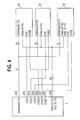
- FIG. 4shows the pin implementation of a memory controller 2 according to a second embodiment of the invention.
- the memory controlleris arranged to operate with three types of memory: Flash memory 42 , first SDRAM 44 and second SDRAM 46 .
- a first pin 201outputs the first 14 bits of the address for the SDRAM memory 44 or 46 and the last 6 bits (bits 16 - 21 ) of the address for the Flash memory 42 .
- Pin 202outputs the 16 bit data for the SDRAM memory and the 16 bit data or the 16 MSB of the address for the Flash memory 42 .
- Pin 203outputs the chip select signal CS 1 for the Flash memory 42 .
- Pin 204outputs the chip select signal CS 2 for the SDRAM memory 44 .
- Pin 205outputs the chip select signal CS 3 for the SDRAM memory 46 .
- Pin 206outputs a Clock Enable signal CKE 1 for the Flash memory 42 .
- Pin 207outputs a CKE 2 signal for the SDRAM memory 44 .
- Pin 208outputs a CKE 3 signal for the SDRAM memory 46 .
- the memory controllermay also include Read Only Memory (ROM) 29 . This is used to store the code used by the device on start-up. When the microprocessor is reset (e.g. the device is switched on) the microprocessor 6 interrogates the ROM. Stored in the ROM is information regarding the type of memory to be accessed when the device is reset. For instance the ROM may include instructions that the memory controller should always access the Flash memory on reset.
- the Flash memorymay store information regarding the address ranges to be used by the memory controller 2 . This information is read by the microprocessor and stored in the address decoder 22 of the memory controller. The address information (i.e. ranges and type of memory) may either be hardwired into the address decoder 22 or this information may be downloaded from the boot ROM 29 .
- the memory controller 2 or boot ROM 29may be programmed with instructions as to how and from where to download this information.
- the method for accessing the first memorycan be found from the BOOT ROM/hardwired logic of the memory controller, then the device will gain access to the first memory during boot up and by downloading information from the first memory it will gain access to other memories.
- the devicemay access this information via an external interface (such as RS232) during boot up from Boot ROM 29 or the hardwired logic of memory controller 2 and by using this interface it may download information needed for accessing memories.
- an external interfacesuch as RS232
Landscapes
- Engineering & Computer Science (AREA)
- Theoretical Computer Science (AREA)
- Physics & Mathematics (AREA)
- General Engineering & Computer Science (AREA)
- General Physics & Mathematics (AREA)
- Dram (AREA)
Abstract
Description
Claims (19)
Applications Claiming Priority (3)
| Application Number | Priority Date | Filing Date | Title |
|---|---|---|---|
| GB9930413AGB2357602A (en) | 1999-12-22 | 1999-12-22 | Memory controller for a memory array comprising different memory types |
| GB9930413 | 1999-12-22 | ||
| GB9930413.1 | 1999-12-22 |
Publications (2)
| Publication Number | Publication Date |
|---|---|
| US20010019509A1 US20010019509A1 (en) | 2001-09-06 |
| US6563739B2true US6563739B2 (en) | 2003-05-13 |
Family
ID=10866881
Family Applications (1)
| Application Number | Title | Priority Date | Filing Date |
|---|---|---|---|
| US09/740,802Expired - LifetimeUS6563739B2 (en) | 1999-12-22 | 2000-12-21 | System and method for transferring data between different types of memory using a common data bus |
Country Status (3)
| Country | Link |
|---|---|
| US (1) | US6563739B2 (en) |
| EP (1) | EP1132819A2 (en) |
| GB (1) | GB2357602A (en) |
Cited By (6)
| Publication number | Priority date | Publication date | Assignee | Title |
|---|---|---|---|---|
| US20020046306A1 (en)* | 2000-03-03 | 2002-04-18 | Hideaki Io | Entertainment apparatus |
| US20070247933A1 (en)* | 2006-04-24 | 2007-10-25 | Sandisk Corporation | Method of High-Performance Flash Memory Data Transfer |
| US20080019189A1 (en)* | 2006-07-19 | 2008-01-24 | Sandisk Corporation | Method of High-Performance Flash Memory Data Transfer |
| US20080019196A1 (en)* | 2006-07-19 | 2008-01-24 | Sandisk Corporation | High-Performance Flash Memory Data Transfer |
| US20090037641A1 (en)* | 2007-07-31 | 2009-02-05 | Bresniker Kirk M | Memory controller with multi-protocol interface |
| US20120131267A1 (en)* | 2006-03-13 | 2012-05-24 | Micron Technology, Inc. | Memory device distributed controller system |
Families Citing this family (42)
| Publication number | Priority date | Publication date | Assignee | Title |
|---|---|---|---|---|
| WO2002048860A2 (en)* | 2000-12-14 | 2002-06-20 | Psion Digital Limited | Synchronous memory controller |
| WO2003021800A1 (en)* | 2001-08-29 | 2003-03-13 | Analog Devices, Inc. | Methods and apparatus for clock and power control in wireless systems |
| WO2004051484A2 (en)* | 2002-12-05 | 2004-06-17 | Nokia Corporation | Device and method for operating memory components |
| JP2004348464A (en)* | 2003-05-22 | 2004-12-09 | Hitachi Ltd | Storage device and communication signal shaping circuit |
| JP4060235B2 (en) | 2003-05-22 | 2008-03-12 | 株式会社日立製作所 | Disk array device and disk array device control method |
| JP4156499B2 (en)* | 2003-11-28 | 2008-09-24 | 株式会社日立製作所 | Disk array device |
| JP4497918B2 (en)* | 2003-12-25 | 2010-07-07 | 株式会社日立製作所 | Storage system |
| JP4634049B2 (en) | 2004-02-04 | 2011-02-16 | 株式会社日立製作所 | Error notification control in disk array system |
| US9507739B2 (en) | 2005-06-24 | 2016-11-29 | Google Inc. | Configurable memory circuit system and method |
| US8359187B2 (en) | 2005-06-24 | 2013-01-22 | Google Inc. | Simulating a different number of memory circuit devices |
| US8055833B2 (en) | 2006-10-05 | 2011-11-08 | Google Inc. | System and method for increasing capacity, performance, and flexibility of flash storage |
| US8130560B1 (en) | 2006-11-13 | 2012-03-06 | Google Inc. | Multi-rank partial width memory modules |
| US7609567B2 (en) | 2005-06-24 | 2009-10-27 | Metaram, Inc. | System and method for simulating an aspect of a memory circuit |
| US8081474B1 (en) | 2007-12-18 | 2011-12-20 | Google Inc. | Embossed heat spreader |
| US8386722B1 (en) | 2008-06-23 | 2013-02-26 | Google Inc. | Stacked DIMM memory interface |
| US9171585B2 (en) | 2005-06-24 | 2015-10-27 | Google Inc. | Configurable memory circuit system and method |
| US10013371B2 (en) | 2005-06-24 | 2018-07-03 | Google Llc | Configurable memory circuit system and method |
| US8060774B2 (en) | 2005-06-24 | 2011-11-15 | Google Inc. | Memory systems and memory modules |
| US8111566B1 (en) | 2007-11-16 | 2012-02-07 | Google, Inc. | Optimal channel design for memory devices for providing a high-speed memory interface |
| US8090897B2 (en) | 2006-07-31 | 2012-01-03 | Google Inc. | System and method for simulating an aspect of a memory circuit |
| US8077535B2 (en) | 2006-07-31 | 2011-12-13 | Google Inc. | Memory refresh apparatus and method |
| US8397013B1 (en)* | 2006-10-05 | 2013-03-12 | Google Inc. | Hybrid memory module |
| US8327104B2 (en) | 2006-07-31 | 2012-12-04 | Google Inc. | Adjusting the timing of signals associated with a memory system |
| US8438328B2 (en)* | 2008-02-21 | 2013-05-07 | Google Inc. | Emulation of abstracted DIMMs using abstracted DRAMs |
| US20080082763A1 (en) | 2006-10-02 | 2008-04-03 | Metaram, Inc. | Apparatus and method for power management of memory circuits by a system or component thereof |
| US9542352B2 (en) | 2006-02-09 | 2017-01-10 | Google Inc. | System and method for reducing command scheduling constraints of memory circuits |
| US20080028136A1 (en) | 2006-07-31 | 2008-01-31 | Schakel Keith R | Method and apparatus for refresh management of memory modules |
| US8796830B1 (en) | 2006-09-01 | 2014-08-05 | Google Inc. | Stackable low-profile lead frame package |
| US7386656B2 (en) | 2006-07-31 | 2008-06-10 | Metaram, Inc. | Interface circuit system and method for performing power management operations in conjunction with only a portion of a memory circuit |
| US8089795B2 (en) | 2006-02-09 | 2012-01-03 | Google Inc. | Memory module with memory stack and interface with enhanced capabilities |
| US8041881B2 (en) | 2006-07-31 | 2011-10-18 | Google Inc. | Memory device with emulated characteristics |
| US8244971B2 (en) | 2006-07-31 | 2012-08-14 | Google Inc. | Memory circuit system and method |
| US8335894B1 (en) | 2008-07-25 | 2012-12-18 | Google Inc. | Configurable memory system with interface circuit |
| WO2007028109A2 (en) | 2005-09-02 | 2007-03-08 | Metaram, Inc. | Methods and apparatus of stacking drams |
| US9632929B2 (en) | 2006-02-09 | 2017-04-25 | Google Inc. | Translating an address associated with a command communicated between a system and memory circuits |
| EP4451270A3 (en) | 2007-04-12 | 2024-12-25 | Rambus Inc. | Memory system with point-to point request interconnect |
| US8080874B1 (en) | 2007-09-14 | 2011-12-20 | Google Inc. | Providing additional space between an integrated circuit and a circuit board for positioning a component therebetween |
| DE202010017690U1 (en) | 2009-06-09 | 2012-05-29 | Google, Inc. | Programming dimming terminating resistor values |
| US10360143B2 (en)* | 2010-07-01 | 2019-07-23 | Qualcomm Incorporated | Parallel use of integrated non-volatile memory and main volatile memory within a mobile device |
| US9323457B2 (en)* | 2013-12-09 | 2016-04-26 | Xilinx, Inc. | Memory arrangement for implementation of high-throughput key-value stores |
| US9711194B2 (en)* | 2015-01-28 | 2017-07-18 | Xilinx, Inc. | Circuits for and methods of controlling the operation of a hybrid memory system |
| US20230236742A1 (en)* | 2022-01-22 | 2023-07-27 | Micron Technology, Inc. | NONVOLATILE MEMORY EXPRESS (NVMe) OVER COMPUTE EXPRESS LINK (CXL) |
Citations (10)
| Publication number | Priority date | Publication date | Assignee | Title |
|---|---|---|---|---|
| US4281392A (en) | 1979-05-01 | 1981-07-28 | Allen-Bradley Company | Memory circuit for programmable machines |
| US5040153A (en) | 1987-10-23 | 1991-08-13 | Chips And Technologies, Incorporated | Addressing multiple types of memory devices |
| US5200600A (en)* | 1988-08-29 | 1993-04-06 | Hitachi Maxell, Ltd. | IC card and method for writing information therein |
| US5528758A (en)* | 1991-11-01 | 1996-06-18 | Yeh; Keming W. | Method and apparatus for providing a portable computer with integrated circuit (IC) memory card storage in custom and standard formats |
| EP0782077A1 (en) | 1995-12-29 | 1997-07-02 | Siemens Aktiengesellschaft | Method and arrangement for converting memory addresses into memory control signals |
| US5838603A (en)* | 1994-10-11 | 1998-11-17 | Matsushita Electric Industrial Co., Ltd. | Semiconductor device and method for fabricating the same, memory core chip and memory peripheral circuit chip |
| US5848247A (en)* | 1994-09-13 | 1998-12-08 | Hitachi, Ltd. | Microprocessor having PC card interface |
| US6026020A (en)* | 1992-03-17 | 2000-02-15 | Hitachi, Ltd. | Data line disturbance free memory block divided flash memory and microcomputer having flash memory therein |
| US6253297B1 (en)* | 1998-04-29 | 2001-06-26 | Texas Instruments Incorporated | Memory control using memory state information for reducing access latency |
| US6273335B1 (en)* | 1998-03-05 | 2001-08-14 | Visa International Service Association | System and method for locking and unlocking an application in a smart card |
- 1999
- 1999-12-22GBGB9930413Apatent/GB2357602A/ennot_activeWithdrawn
- 2000
- 2000-12-15EPEP00311268Apatent/EP1132819A2/ennot_activeWithdrawn
- 2000-12-21USUS09/740,802patent/US6563739B2/ennot_activeExpired - Lifetime
Patent Citations (12)
| Publication number | Priority date | Publication date | Assignee | Title |
|---|---|---|---|---|
| US4281392A (en) | 1979-05-01 | 1981-07-28 | Allen-Bradley Company | Memory circuit for programmable machines |
| US5040153A (en) | 1987-10-23 | 1991-08-13 | Chips And Technologies, Incorporated | Addressing multiple types of memory devices |
| US5200600A (en)* | 1988-08-29 | 1993-04-06 | Hitachi Maxell, Ltd. | IC card and method for writing information therein |
| US5528758A (en)* | 1991-11-01 | 1996-06-18 | Yeh; Keming W. | Method and apparatus for providing a portable computer with integrated circuit (IC) memory card storage in custom and standard formats |
| US5574859A (en)* | 1991-11-01 | 1996-11-12 | Yeh; Keming W. | Method and apparatus for using a software configurable connector to connect a palmtop computer having a custom port to a host having a standard port |
| US5666495A (en)* | 1991-11-01 | 1997-09-09 | Yeh; Keming W. | Method and structure for data transfer between a standard port of a host computer and a custom port of a palmtop computer using a docking station |
| US6026020A (en)* | 1992-03-17 | 2000-02-15 | Hitachi, Ltd. | Data line disturbance free memory block divided flash memory and microcomputer having flash memory therein |
| US5848247A (en)* | 1994-09-13 | 1998-12-08 | Hitachi, Ltd. | Microprocessor having PC card interface |
| US5838603A (en)* | 1994-10-11 | 1998-11-17 | Matsushita Electric Industrial Co., Ltd. | Semiconductor device and method for fabricating the same, memory core chip and memory peripheral circuit chip |
| EP0782077A1 (en) | 1995-12-29 | 1997-07-02 | Siemens Aktiengesellschaft | Method and arrangement for converting memory addresses into memory control signals |
| US6273335B1 (en)* | 1998-03-05 | 2001-08-14 | Visa International Service Association | System and method for locking and unlocking an application in a smart card |
| US6253297B1 (en)* | 1998-04-29 | 2001-06-26 | Texas Instruments Incorporated | Memory control using memory state information for reducing access latency |
Cited By (14)
| Publication number | Priority date | Publication date | Assignee | Title |
|---|---|---|---|---|
| US6823420B2 (en)* | 2000-03-03 | 2004-11-23 | Sony Computer Entertainment Inc. | Entertainment apparatus |
| US20020046306A1 (en)* | 2000-03-03 | 2002-04-18 | Hideaki Io | Entertainment apparatus |
| US10359944B2 (en) | 2006-03-13 | 2019-07-23 | Micron Technology, Inc. | Memory devices having distributed controller systems |
| US9772779B2 (en) | 2006-03-13 | 2017-09-26 | Micron Technology, Inc. | Methods for operating a distributed controller system in a memory device |
| US9317459B2 (en)* | 2006-03-13 | 2016-04-19 | Micron Technology, Inc. | Memory device distributed controller system |
| US20120131267A1 (en)* | 2006-03-13 | 2012-05-24 | Micron Technology, Inc. | Memory device distributed controller system |
| US7525855B2 (en)* | 2006-04-24 | 2009-04-28 | Sandisk Corporation | Method of high-performance flash memory data transfer |
| US20070247933A1 (en)* | 2006-04-24 | 2007-10-25 | Sandisk Corporation | Method of High-Performance Flash Memory Data Transfer |
| US20080019189A1 (en)* | 2006-07-19 | 2008-01-24 | Sandisk Corporation | Method of High-Performance Flash Memory Data Transfer |
| US7499369B2 (en) | 2006-07-19 | 2009-03-03 | Sandisk Corporation | Method of high-performance flash memory data transfer |
| US7499339B2 (en)* | 2006-07-19 | 2009-03-03 | Sandisk Corporation | High-performance flash memory data transfer |
| US20080019196A1 (en)* | 2006-07-19 | 2008-01-24 | Sandisk Corporation | High-Performance Flash Memory Data Transfer |
| US8347005B2 (en)* | 2007-07-31 | 2013-01-01 | Hewlett-Packard Development Company, L.P. | Memory controller with multi-protocol interface |
| US20090037641A1 (en)* | 2007-07-31 | 2009-02-05 | Bresniker Kirk M | Memory controller with multi-protocol interface |
Also Published As
| Publication number | Publication date |
|---|---|
| GB2357602A (en) | 2001-06-27 |
| US20010019509A1 (en) | 2001-09-06 |
| GB9930413D0 (en) | 2000-02-16 |
| EP1132819A2 (en) | 2001-09-12 |
Similar Documents
| Publication | Publication Date | Title |
|---|---|---|
| US6563739B2 (en) | System and method for transferring data between different types of memory using a common data bus | |
| KR100867900B1 (en) | Sdram memory device with an embedded nand flash controller | |
| US7930530B2 (en) | Multi-processor system that reads one of a plurality of boot codes via memory interface buffer in response to requesting processor | |
| US6771526B2 (en) | Method and apparatus for data transfer | |
| KR100262030B1 (en) | Memory system and semiconductor memory device used therefor | |
| US20040017724A1 (en) | Semiconductor processing device | |
| US6888733B2 (en) | Multiple chip system including a plurality of non-volatile semiconductor memory devices | |
| US6601130B1 (en) | Memory interface unit with programmable strobes to select different memory devices | |
| US5787299A (en) | Pin selection system for microcontroller having multiplexer selects between address/data signals and special signals produced by special function device | |
| US20080195795A1 (en) | Pipelined burst memory access | |
| US4849931A (en) | Data processing system having interfacing circuits assigned to a common I/O port address by utilizing a specific bit line of a common bus | |
| US6584528B1 (en) | Microprocessor allocating no wait storage of variable capacity to plurality of resources, and memory device therefor | |
| US7162563B2 (en) | Semiconductor integrated circuit having changeable bus width of external data signal | |
| US20050144372A1 (en) | Memory device controlled with user-defined commands | |
| US20070028037A1 (en) | Memory system with automatic dual-buffering | |
| US6754760B1 (en) | Programmable interface for a configurable system bus | |
| US6725346B1 (en) | Method and apparatus for overlaying memory in a data processing system | |
| JP2003223412A (en) | Semiconductor integrated circuit | |
| KR20040045446A (en) | Interfacing processors with external memory supporting burst mode | |
| US6813697B1 (en) | Data processor and data processing system | |
| US6202140B1 (en) | Memory addressing system and method therefor | |
| JP4121373B2 (en) | Harvard architecture microprocessor with linear addressable space. | |
| GB2304209A (en) | Starting up a processor system | |
| KR100526531B1 (en) | Address Decoding Circuit of Memory Device | |
| KR940003328B1 (en) | Map network interface device |
Legal Events
| Date | Code | Title | Description |
|---|---|---|---|
| AS | Assignment | Owner name:NOKIA MOBILE PHONES LIMITED, FINLAND Free format text:ASSIGNMENT OF ASSIGNORS INTEREST;ASSIGNORS:AHO, ARI;FLOMAN, MATTI;LIPPONEN, MARRKU;REEL/FRAME:011714/0300;SIGNING DATES FROM 20010322 TO 20010326 | |
| AS | Assignment | Owner name:NOKIA MOBILE PHONES LIMITED, FINLAND Free format text:ASSIGNMENT OF ASSIGNORS INTEREST;ASSIGNORS:AHO, ARI;FLOMAN, MATTI;LIPPONEN, MARKKU;REEL/FRAME:012318/0240;SIGNING DATES FROM 20010322 TO 20010326 | |
| STCF | Information on status: patent grant | Free format text:PATENTED CASE | |
| FPAY | Fee payment | Year of fee payment:4 | |
| FPAY | Fee payment | Year of fee payment:8 | |
| FPAY | Fee payment | Year of fee payment:12 | |
| AS | Assignment | Owner name:NOKIA TECHNOLOGIES OY, FINLAND Free format text:ASSIGNMENT OF ASSIGNORS INTEREST;ASSIGNOR:NOKIA CORPORATION;REEL/FRAME:036067/0222 Effective date:20150116 | |
| AS | Assignment | Owner name:PROVENANCE ASSET GROUP LLC, CONNECTICUT Free format text:ASSIGNMENT OF ASSIGNORS INTEREST;ASSIGNORS:NOKIA TECHNOLOGIES OY;NOKIA SOLUTIONS AND NETWORKS BV;ALCATEL LUCENT SAS;REEL/FRAME:043877/0001 Effective date:20170912 Owner name:NOKIA USA INC., CALIFORNIA Free format text:SECURITY INTEREST;ASSIGNORS:PROVENANCE ASSET GROUP HOLDINGS, LLC;PROVENANCE ASSET GROUP LLC;REEL/FRAME:043879/0001 Effective date:20170913 Owner name:CORTLAND CAPITAL MARKET SERVICES, LLC, ILLINOIS Free format text:SECURITY INTEREST;ASSIGNORS:PROVENANCE ASSET GROUP HOLDINGS, LLC;PROVENANCE ASSET GROUP, LLC;REEL/FRAME:043967/0001 Effective date:20170913 | |
| AS | Assignment | Owner name:NOKIA US HOLDINGS INC., NEW JERSEY Free format text:ASSIGNMENT AND ASSUMPTION AGREEMENT;ASSIGNOR:NOKIA USA INC.;REEL/FRAME:048370/0682 Effective date:20181220 | |
| AS | Assignment | Owner name:PROVENANCE ASSET GROUP LLC, CONNECTICUT Free format text:RELEASE BY SECURED PARTY;ASSIGNOR:CORTLAND CAPITAL MARKETS SERVICES LLC;REEL/FRAME:058983/0104 Effective date:20211101 Owner name:PROVENANCE ASSET GROUP HOLDINGS LLC, CONNECTICUT Free format text:RELEASE BY SECURED PARTY;ASSIGNOR:CORTLAND CAPITAL MARKETS SERVICES LLC;REEL/FRAME:058983/0104 Effective date:20211101 Owner name:PROVENANCE ASSET GROUP LLC, CONNECTICUT Free format text:RELEASE BY SECURED PARTY;ASSIGNOR:NOKIA US HOLDINGS INC.;REEL/FRAME:058363/0723 Effective date:20211129 Owner name:PROVENANCE ASSET GROUP HOLDINGS LLC, CONNECTICUT Free format text:RELEASE BY SECURED PARTY;ASSIGNOR:NOKIA US HOLDINGS INC.;REEL/FRAME:058363/0723 Effective date:20211129 | |
| AS | Assignment | Owner name:RPX CORPORATION, CALIFORNIA Free format text:ASSIGNMENT OF ASSIGNORS INTEREST;ASSIGNOR:PROVENANCE ASSET GROUP LLC;REEL/FRAME:059352/0001 Effective date:20211129 |