US6563183B1 - Gate array with multiple dielectric properties and method for forming same - Google Patents
Gate array with multiple dielectric properties and method for forming sameDownload PDFInfo
- Publication number
- US6563183B1 US6563183B1US10/085,949US8594902AUS6563183B1US 6563183 B1US6563183 B1US 6563183B1US 8594902 AUS8594902 AUS 8594902AUS 6563183 B1US6563183 B1US 6563183B1
- Authority
- US
- United States
- Prior art keywords
- dielectric layer
- dielectric
- channel region
- integrated circuit
- gate
- Prior art date
- Legal status (The legal status is an assumption and is not a legal conclusion. Google has not performed a legal analysis and makes no representation as to the accuracy of the status listed.)
- Expired - Fee Related
Links
- 238000000034methodMethods0.000titledescription50
- 229910021420polycrystalline siliconInorganic materials0.000claimsabstractdescription71
- 229920005591polysiliconPolymers0.000claimsabstractdescription71
- 239000000758substrateSubstances0.000claimsabstractdescription46
- 239000003989dielectric materialSubstances0.000claimsabstractdescription26
- 230000005669field effectEffects0.000claimsabstractdescription20
- 239000004065semiconductorSubstances0.000claimsabstractdescription18
- 239000000463materialSubstances0.000claimsdescription40
- GWEVSGVZZGPLCZ-UHFFFAOYSA-NTitan oxideChemical compoundO=[Ti]=OGWEVSGVZZGPLCZ-UHFFFAOYSA-N0.000claimsdescription14
- MCMNRKCIXSYSNV-UHFFFAOYSA-NZirconium dioxideChemical compoundO=[Zr]=OMCMNRKCIXSYSNV-UHFFFAOYSA-N0.000claimsdescription8
- RUDFQVOCFDJEEF-UHFFFAOYSA-Nyttrium(III) oxideInorganic materials[O-2].[O-2].[O-2].[Y+3].[Y+3]RUDFQVOCFDJEEF-UHFFFAOYSA-N0.000claimsdescription7
- PNEYBMLMFCGWSK-UHFFFAOYSA-Naluminium oxideInorganic materials[O-2].[O-2].[O-2].[Al+3].[Al+3]PNEYBMLMFCGWSK-UHFFFAOYSA-N0.000claimsdescription4
- CETPSERCERDGAM-UHFFFAOYSA-Nceric oxideChemical compoundO=[Ce]=OCETPSERCERDGAM-UHFFFAOYSA-N0.000claimsdescription4
- 229910000422cerium(IV) oxideInorganic materials0.000claimsdescription4
- 229910052593corundumInorganic materials0.000claimsdescription4
- CJNBYAVZURUTKZ-UHFFFAOYSA-Nhafnium(IV) oxideInorganic materialsO=[Hf]=OCJNBYAVZURUTKZ-UHFFFAOYSA-N0.000claimsdescription4
- 229910044991metal oxideInorganic materials0.000claimsdescription4
- 150000004706metal oxidesChemical group0.000claimsdescription4
- 229910001845yogo sapphireInorganic materials0.000claimsdescription4
- 229910002938(Ba,Sr)TiO3Inorganic materials0.000claimsdescription3
- 229910003781PbTiO3Inorganic materials0.000claimsdescription3
- 229910002370SrTiO3Inorganic materials0.000claimsdescription3
- 150000004645aluminatesChemical class0.000claimsdescription3
- 229910052454barium strontium titanateInorganic materials0.000claimsdescription3
- 229910002113barium titanateInorganic materials0.000claimsdescription3
- MRELNEQAGSRDBK-UHFFFAOYSA-Nlanthanum oxideInorganic materials[O-2].[O-2].[O-2].[La+3].[La+3]MRELNEQAGSRDBK-UHFFFAOYSA-N0.000claimsdescription3
- 229910052451lead zirconate titanateInorganic materials0.000claimsdescription3
- KTUFCUMIWABKDW-UHFFFAOYSA-Noxo(oxolanthaniooxy)lanthanumChemical compoundO=[La]O[La]=OKTUFCUMIWABKDW-UHFFFAOYSA-N0.000claimsdescription3
- 150000004760silicatesChemical class0.000claimsdescription3
- PBCFLUZVCVVTBY-UHFFFAOYSA-Ntantalum pentoxideInorganic materialsO=[Ta](=O)O[Ta](=O)=OPBCFLUZVCVVTBY-UHFFFAOYSA-N0.000claimsdescription3
- VYPSYNLAJGMNEJ-UHFFFAOYSA-NSilicium dioxideChemical compoundO=[Si]=OVYPSYNLAJGMNEJ-UHFFFAOYSA-N0.000abstractdescription24
- 235000012239silicon dioxideNutrition0.000abstractdescription12
- 239000000377silicon dioxideSubstances0.000abstractdescription12
- 229920002120photoresistant polymerPolymers0.000description48
- 238000000151depositionMethods0.000description32
- 238000004519manufacturing processMethods0.000description30
- 238000005530etchingMethods0.000description14
- 230000008569processEffects0.000description14
- XUIMIQQOPSSXEZ-UHFFFAOYSA-NSiliconChemical compound[Si]XUIMIQQOPSSXEZ-UHFFFAOYSA-N0.000description9
- 238000005286illuminationMethods0.000description9
- 238000001459lithographyMethods0.000description9
- 229910052710siliconInorganic materials0.000description9
- 239000010703siliconSubstances0.000description9
- 230000004888barrier functionEffects0.000description8
- 230000001427coherent effectEffects0.000description6
- 238000000059patterningMethods0.000description6
- 239000006117anti-reflective coatingSubstances0.000description5
- 230000008878couplingEffects0.000description4
- 238000010168coupling processMethods0.000description4
- 238000005859coupling reactionMethods0.000description4
- 238000010586diagramMethods0.000description4
- 230000004048modificationEffects0.000description4
- 238000012986modificationMethods0.000description4
- 230000003667anti-reflective effectEffects0.000description3
- 238000000231atomic layer depositionMethods0.000description3
- 229910021419crystalline siliconInorganic materials0.000description3
- 230000003247decreasing effectEffects0.000description3
- 238000005137deposition processMethods0.000description3
- 238000010849ion bombardmentMethods0.000description3
- 238000004518low pressure chemical vapour depositionMethods0.000description3
- 230000003647oxidationEffects0.000description3
- 238000007254oxidation reactionMethods0.000description3
- 125000006850spacer groupChemical group0.000description3
- 238000005406washingMethods0.000description3
- 230000000694effectsEffects0.000description2
- 150000004767nitridesChemical class0.000description2
- 241000237519BivalviaSpecies0.000description1
- 238000003491arrayMethods0.000description1
- 230000008901benefitEffects0.000description1
- 235000020639clamNutrition0.000description1
- 239000011248coating agentSubstances0.000description1
- 238000000576coating methodMethods0.000description1
- 239000011261inert gasSubstances0.000description1
- 238000002347injectionMethods0.000description1
- 239000007924injectionSubstances0.000description1
- 230000000873masking effectEffects0.000description1
- 238000005498polishingMethods0.000description1
- 238000000926separation methodMethods0.000description1
- 230000005641tunnelingEffects0.000description1
Images


Classifications
- H—ELECTRICITY
- H10—SEMICONDUCTOR DEVICES; ELECTRIC SOLID-STATE DEVICES NOT OTHERWISE PROVIDED FOR
- H10D—INORGANIC ELECTRIC SEMICONDUCTOR DEVICES
- H10D84/00—Integrated devices formed in or on semiconductor substrates that comprise only semiconducting layers, e.g. on Si wafers or on GaAs-on-Si wafers
- H10D84/01—Manufacture or treatment
- H10D84/0123—Integrating together multiple components covered by H10D12/00 or H10D30/00, e.g. integrating multiple IGBTs
- H10D84/0126—Integrating together multiple components covered by H10D12/00 or H10D30/00, e.g. integrating multiple IGBTs the components including insulated gates, e.g. IGFETs
- H10D84/013—Manufacturing their source or drain regions, e.g. silicided source or drain regions
- H10D84/0133—Manufacturing common source or drain regions between multiple IGFETs
- H—ELECTRICITY
- H10—SEMICONDUCTOR DEVICES; ELECTRIC SOLID-STATE DEVICES NOT OTHERWISE PROVIDED FOR
- H10D—INORGANIC ELECTRIC SEMICONDUCTOR DEVICES
- H10D84/00—Integrated devices formed in or on semiconductor substrates that comprise only semiconducting layers, e.g. on Si wafers or on GaAs-on-Si wafers
- H10D84/01—Manufacture or treatment
- H10D84/0123—Integrating together multiple components covered by H10D12/00 or H10D30/00, e.g. integrating multiple IGBTs
- H10D84/0126—Integrating together multiple components covered by H10D12/00 or H10D30/00, e.g. integrating multiple IGBTs the components including insulated gates, e.g. IGFETs
- H10D84/0144—Manufacturing their gate insulating layers
- H—ELECTRICITY
- H10—SEMICONDUCTOR DEVICES; ELECTRIC SOLID-STATE DEVICES NOT OTHERWISE PROVIDED FOR
- H10D—INORGANIC ELECTRIC SEMICONDUCTOR DEVICES
- H10D84/00—Integrated devices formed in or on semiconductor substrates that comprise only semiconducting layers, e.g. on Si wafers or on GaAs-on-Si wafers
- H10D84/01—Manufacture or treatment
- H10D84/02—Manufacture or treatment characterised by using material-based technologies
- H10D84/03—Manufacture or treatment characterised by using material-based technologies using Group IV technology, e.g. silicon technology or silicon-carbide [SiC] technology
- H10D84/038—Manufacture or treatment characterised by using material-based technologies using Group IV technology, e.g. silicon technology or silicon-carbide [SiC] technology using silicon technology, e.g. SiGe
Definitions
- the present inventionrelates to methods for fabricating an array of field effect transistors on a semiconductor substrate, and more particularly for fabricating an array wherein each gate has a the gate dielectric with dielectric properties independent of other gates in the array.
- Integrated circuitstypically utilize an array of field effect transistors, each of which comprises a polysilicon gate positioned over a channel region within a silicon substrate.
- An insulating layertypically called a gate oxide, separates the polysilicon gate from the channel region.
- the typical process for fabricating a polysilicon gateis to first grow an oxide on the surface of a substrate followed by applying a polysilicon layer. An anti-reflective coating and a photoresist layer are then deposited over the polysilicon layer, patterned, and-developed to mask the polysilicon gate. An anisotropic etch is then used to remove the un-masked polysilicon such that the polysilicon gate is formed.
- Decreasing the gate sizepermits decreasing the size of each individual silicon device. Decreasing the size of each device provides the ability to increase the density of the transistor array fabricated on the substrate which provides the ability to fabricate a more complex circuit on a substrate of a given size. Additionally, a smaller channel region beneath a smaller gate reduces capacitance across the channel/source junction and the channel drain junction which provides for faster operating speed and reduced power consumption.
- Reducing the gate sizerequires reducing the thickness of the gate oxide to maintain adequate capacitive coupling between the gate and the channel region. Further, there exists a minimum physical thickness of the gate oxide at which the oxide no longer isolates the gate from the channel region. Therefore, there exists a minimum gate size that can be achieved when silicon dioxide is used as the gate oxide. Therefore, it has been proposed to use other dielectrics with dielectric constants greater than the dielectric constant of silicon dioxide (e.g high K dielectrics) in the dielectric layer to replace silicon dioxide such that capacitive coupling is improved (e.g. smaller electrical thickness) while a larger physical thickness is maintained. With the use of high K dielectrics, very small transistor structures and dense transistor arrays can be fabricated. It is envisioned that such complex circuits will require the use of transistors with different operating properties.
- each transistormay be fabricated with a gate dielectric that includes dielectric properties independent of dielectric properties of adjacent transistors.
- a first aspect of the present inventionis to provide an integrated circuit fabricated on a semiconductor substrate.
- the integrated circuitcomprises a first field effect transistor and a second field effect transistor.
- the first field effect transistorcomprises a first polysilicon gate positioned above a first channel region of the substrate and isolated from the first channel region by a first dielectric layer extending the entire length of the first polysilicon gate.
- the first dielectric layercomprises a first dielectric material with a first dielectric constant.
- the second field effect transistorcomprises a second polysilicon gate positioned above a second channel region on the substrate and isolated from the second channel region by a second dielectric layer extending the entire length of the second polysilicon gate.
- the second dielectric layercomprises a second dielectric material with a second dielectric constant.
- the first dielectric constant and the second dielectric constantmay be different and both may be greater than the dielectric constant of silicon dioxide.
- the second dielectric layermay itself comprise multiple layers.
- the second dielectric layermay comprise a third dielectric layer adjacent to the second dielectric layer (and adjacent to either the second polysilicon gate or adjacent to the substrate) extending the entire length of the second polysilicon gate.
- the third dielectric layermay comprise a third dielectric material which may, or may not, be the same as the first dielectric material.
- the thickness of the first dielectric layer and the second dielectric layer(as measured between the substrate and the polysilicon gate) may or may not be the same. Further, the thickness of the first polysilicon gate and the second polysilicon gate may or may not be the same.
- a second aspect of the present inventionis to provide a method of fabricating an integrated circuit on a semiconductor substrate.
- the methodcomprises: a) depositing a first high K dielectric on the substrate; b) fabricating a mask on the surface of the first high K dielectric to mask a first portion and to expose a second portion; c) removing the first high K dielectric to expose the substrate in the second portion; d) depositing a second high K dielectric on the substrate in the second portion; e) depositing a polysilicon layer over the first portion and the second portion; f) fabricating a mask on the surface of the polysilicon layer to mask a first gate in the first portion and to mask a second gate in the second portion; and g) etching the polysilicon layer, the first high K dielectric and the second high K dielectric to form the first gate and the second gate.
- the step of depositing the second high K dielectric on the substrate in the second portionmay comprise depositing the second high K dielectric over the entire surface including the substrate in the second portion and at least one of the mask and the first high K dielectric in the first portion. Thereafter, the wafer may be polished to expose the first high K dielectric in the first portion.
- a third aspect of the present inventionis to provide an alternative method of fabricating an integrated circuit on a semiconductor substrate.
- the alternative methodcomprises: a) depositing a first high K dielectric on the substrate; b) fabricating a mask on the surface of the first high K dielectric to mask a first portion and to expose a second portion; c) altering the dielectric properties of the first high K dielectric in the second portion; d) depositing a polysilicon layer over the first portion and the second portion; e) fabricating a mask on the surface of the polysilicon layer to mask a first gate in the first portion and to mask a second gate in the second portion; and f) etching the polysilicon layer, the first high K dielectric, and the second high K dielectric to form the first gate and the second gate.
- the step of altering the dielectric property of the first high K dielectricmay comprise implanting the first high K dielectric with at least one of N + , Hf + , Al + , and Zr + .
- the step of altering the dielectric property of the first high K dielectricmay comprise subjecting the first high K dielectric to a plasma environment to modify the work function of the first high K dielectric.
- a fourth aspect of the present inventionis to provide yet another alternative method of fabricating an integrated circuit on a semiconductor substrate.
- the methodcomprising: a) depositing a first high K dielectric on the substrate; b) fabricating a mask on the surface of the first high K dielectric to mask a first portion and to expose a second portion; c) removing the first high K dielectric to expose the substrate in the second portion; d) altering the dielectric properties of the first high K dielectric in the second portion; e) depositing a second high K dielectric on the substrate in the second portion; f) depositing a polysilicon layer over the first portion and the second portion; g) fabricating a mask on the surface of the polysilicon layer to mask a first gate in the first portion and to mask a second gate in the second portion; and h) etching the polysilicon layer, the first high K dielectric, and the second high K dielectric to form the first gate and the second gate.
- the step of altering the dielectric property of the first high K dielectricmay comprise implanting the first high K dielectric with at least one of N + , Hf + , Al + , and Zr + .
- the step of altering the dielectric property of the first high K dielectricmay comprise subjecting the first high K dielectric to a plasma environment to modify the work function of the first high K dielectric.
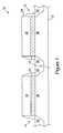
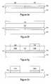
- FIG. 1is a schematic cross sectional view of an integrated circuit in accordance with one embodiment of the present invention.
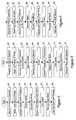
- FIG. 2is a flow chart representing a method of fabricating an integrated circuit in accordance with one embodiment of the present invention
- FIG. 3is a flow chart representing a method of fabricating an integrated circuit in accordance with one embodiment of the present invention
- FIG. 4is a flow chart representing a method of fabricating an integrated circuit in accordance with one embodiment of the present invention.
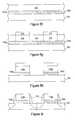
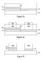
- FIG. 5 ais a cross sectional view of one processing step in the fabrication of the integrated circuit in accordance with the method of the flowchart of FIG. 2;
- FIG. 5 bis a cross sectional view of one processing step in the fabrication of the integrated circuit in accordance with the method of the flowchart of FIG. 2;
- FIG. 5 cis a cross sectional view of one processing step in the fabrication of the integrated circuit in accordance with the method of the flowchart of FIG. 2;
- FIG. 5 dis a cross sectional view of one processing step in the fabrication of the integrated circuit in accordance with the method of the flowchart of FIG. 2;
- FIG. 5 eis a cross sectional view of one processing step in the fabrication of the integrated circuit in accordance with the method of the flowchart of FIG. 2;
- FIG. 5 fis a cross sectional view of one processing step in the fabrication of the integrated circuit in accordance with the method of the flowchart of FIG. 2;
- FIG. 5 gis a cross sectional view of one processing step in the fabrication of the integrated circuit in accordance with the method of the flowchart of FIG. 2;
- FIG. 5 his a cross sectional view of one processing step in the fabrication of the integrated circuit in accordance with the method of the flowchart of FIG. 2;
- FIG. 5 iis a cross sectional view of one processing step in the fabrication of the integrated circuit in accordance with the method of the flowchart of FIG. 2;
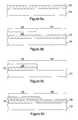
- FIG. 6 ais a cross sectional view of one processing step in the fabrication of the integrated circuit in accordance with the method of the flowchart of FIG. 3;
- FIG. 6 bis a cross sectional view of one processing step in the fabrication of the integrated circuit in accordance with the method of the flowchart of FIG. 3;
- FIG. 6 cis a cross sectional view of one processing step in the fabrication of the integrated circuit in accordance with the method of the flowchart of FIG. 3;
- FIG. 6 dis a cross sectional view of one processing step in the fabrication of the integrated circuit in accordance with the method of the flowchart of FIG. 3;
- FIG. 6 eis a cross sectional view of one processing step in the fabrication of the integrated circuit in accordance with the method of the flowchart of FIG. 3;
- FIG. 6 fis a cross sectional view of one processing step in the fabrication of the integrated circuit in accordance with the method of the flowchart of FIG. 3;
- FIG. 6 gis a cross sectional view of one processing step in the fabrication of the integrated circuit in accordance with the method of the flowchart of FIG. 3;
- FIG. 6 his a cross sectional view of one processing step in the fabrication of the integrated circuit in accordance with the method of the flowchart of FIG. 3;
- FIG. 7 ais a cross sectional view of one processing step in the fabrication of the integrated circuit in accordance with the method of the flowchart of FIG. 4;
- FIG. 7 bis a cross sectional view of one processing step in the fabrication of the integrated circuit in accordance with the method of the flowchart of FIG. 4;
- FIG. 7 cis a cross sectional view of one processing step in the fabrication of the integrated circuit in accordance with the method of the flowchart of FIG. 4;
- FIG. 7 dis a cross sectional view of one processing step in the fabrication of the integrated circuit in accordance with the method of the flowchart of FIG. 4;
- FIG. 7 eis a cross sectional view of one processing step in the fabrication of the integrated circuit in accordance with the method of the flowchart of FIG. 4;
- FIG. 7 fis a cross sectional view of one processing step in the fabrication of the integrated circuit in accordance with the method of the flowchart of FIG. 4 .
- the integrated circuit 10includes two field effect transistors 14 and 16 fabricated on a semiconductor substrate 12 .
- Each field effect transistor 14 and 16comprises a semiconductor gate 18 and 20 respectively positioned horizontally over a channel region 36 and 38 within the substrate 12 .
- a source region 26 and 30 and a drain region 28 and 32are positioned within the substrate 12 adjacent the channel region 36 and 38 respectively and define a length of the channel region 36 and 38 respectively. Because each semiconductor gate 18 and 20 is typically used for masking each channel region 36 and 38 when implanting each source regions 26 and 30 and each drain region 28 and 32 , the length of each channel region 36 and 38 is approximately the same length as the length of the semiconductor gate 18 and 20 that masks such channel region 36 and 38 .
- a first dielectric layer 22isolates the gate 18 from the channel region 36 and a second dielectric layer 24 isolates the gate 20 from the channel region 38 .
- the first dielectric layer 22laterally extends the entire length of the gate 18 and has a physical thickness (separation distance between the channel region 36 and the gate 18 ) adequate to prevent charge from migrating (e.g. charge tunneling or charge injection) between the channel region 36 and the gate 18 .
- the first dielectric layer 22comprises at least one horizontal layer of a dielectric material with a dielectric constant greater than that of silicon dioxide (e.g. high K dielectric material) such that the gate 18 and the channel region 36 capacitively couple through the first dielectric layer 22 as required for operation of field effect transistor 14 .
- the strength of the capacitive coupling required for operation of the field effect transistor 14is a function of the operating speed and voltage of the field effect transistor 14 as well as the physical dimensions and material properties of the gate 18 and the channel region 36 .
- the second dielectric layer 24laterally extends the entire length of the gate 20 and has a physical thickness adequate to prevent charge from migrating between the channel region 38 and the gate 20 .
- the physical thickness of the second dielectric layer 24may be different than the physical thickness of the first dielectric layer 22 .
- the second dielectric layer 24comprises at least one horizontal layer comprising a high K dielectric material such that the gate 20 and the channel region 38 capacitively couple through the second dielectric layer 24 as required for operation of field effect transistor 14 .
- the strength of the capacitive coupling required for operation of the field effect transistor 16is a function of the operating speed and voltage of the field effect transistor 16 as well as the physical dimensions and material properties of the gate 20 and the channel region 38 .
- the material comprising the second dielectric layer 24may be different than the material comprising the first dielectric layer 22 in an embodiment wherein each of the first dielectric layer 22 and the second dielectric layer 24 comprise only a single homogenous material.
- the material comprising at least one horizontal layer of the second dielectric layer 24may be different than at least one horizontal layer of the first dielectric layer 22 in an embodiment wherein at least one of the first dielectric layer 22 and the second dielectric layer 24 comprise multiple horizontal layers of dielectric materials.
- FIG. 5 ashows an exemplary semiconductor substrate 100 such as monocrystaline silicon.
- the monocrystaline silicon substrate 100may be lightly doped either p-type or n-type.
- Step 40 40 orepresents depositing a first high K dielectric layer 102 on the surface of the substrate 100 as is shown in FIG. 5 b .
- the first high K dielectric layer 102may comprise a material selected from the group of TiO 2 , Y 2 O 3 , Ta 2 O 5 , La 2 O 3 ,or their silicates or aluminates, BaTiO 3 , SrTiO 3 , BST ((Ba,Sr)TiO 3 ), PbTiO 3 , PZT, HfO 2 , ZrO 2 , CeO 2 , Al 2 O 3 , TiO 2 , Y 2 O 3 , and other binary and tertiary metal oxides and ferroelectric material having a dielectric constant greater than 20.
- the first high K dielectric layer 102may be deposited on the substrate 100 using a low pressure chemical vapor deposition process. Because some of the high K materials in the group listed above may form an incompatible boundary with crystalline silicon, a barrier interface layer may be formed below the high-K dielectric layer 102 to provide a buffer interface between the high K material and the silicon substrate 100 .
- the buffer interface layermay be silicon dioxide having a thickness of about 0.5 nm to about 0.7 nm and may be deposited on the surface of the silicon substrate 100 prior to the high K dielectric layer 102 using low temperature thermal oxidation, a remote plasma deposition process, an atomic layer deposition process, or a similar process for fabricating silicon dioxide on silicon to an approximate thickness of 0.5 nm-0.7 nm.
- Step 42represents fabricating a mask 104 over a first portion 106 of the first high K dielectric layer 102 .
- the maskmay be a photoresist masked fabricating using typical lithography techniques which may include depositing photoresist across the entire surface of the first high K dielectric layer 102 followed by patterning the photoresist using coherent UV illumination and developing the photoresist to wash away the photoresist over a second portion 108 of the first high K dielectric layer 102 while leaving the mask 104 over the first portion 106 .
- an anti reflective barrier materialmay be deposited over the first high K dielectric layer 102 prior to depositing the photoresist and fabricating the mask 104 .
- Step 44represents modifying the dielectric properties of the first high K dielectric layer 102 in the second portion 108 as is shown in FIG. 5 d .
- Step 44may include exposing the second portion 108 of the high K dielectric layer 102 to a plasma environment to modify the work function of the high K dielectric material.
- step 44may represent implanting the exposed high K dielectric material with at least one of N + , Hf + , Al + , and Zr + .
- the mask 106prevents modification of the high K dielectric material in the first portion 106 .
- Step 46represents removing the photoresist mask 104 leaving both of the first portion 106 and the second portion 108 of the high K dielectric layer 102 exposed. It should be appreciated that after the modification of the dielectric layer 102 in the first portion at step 44 , the first portion no longer has the same dielectric properties as the second portion. As such in FIG. 5 e , the first portion is referred to as the first dielectric layer 102 a and the second portion is referred to as the second dielectric layer 102 b.
- Step 48represents depositing a layer of semiconductor material 110 across both the first dielectric layer 102 a and the second dielectric layer 102 b .
- the layer of semiconductor material 110may be polysilicon. Again, because incompatibility may exist between either the material of the first dielectric layer 102 a and polysilicon or the material of the second dielectric layer 102 b and polysilicon, a barrier interface layer may be deposited on the surface of both the first dielectric layer 102 a and the second dielectric layer 102 b prior to depositing the polysilicon.
- Step 50represents depositing and patterning a gate mask 112 on the surface of the polysilicon layer 110 .
- the maskmay be a photoresist mask fabricating using typical lithography techniques which may include depositing an antireflective coating such as nitride across the entire surface of the polysilicon layer 110 followed by depositing a layer of photoresist across the entire surface of the anti reflective coating.
- the photoresistmay then be patterned using coherent UV illumination and developing the photoresist to harden the photoresist mask 112 in gate regions 114 while washing away the photoresist over other regions.
- Step 52represents etching the polysilicon and the dielectric layers 102 a and 102 b to form the transistor gates 116 a and 116 b over the first dielectric layer 102 a and the second dielectric layer 102 b respectively as is shown in FIG. 5 h .
- Etching of the polysiliconmay include an ion bombardment etch using HBr, CF 4 , CL 2 in combination with HeO 2 to increase the selectivity between the polysilicon and the high K materials.
- Increasing selectivity between the polysilicon and the high K materialenables the polysilicon etch to be performed with an increased bias power and a reduced pressure which improves the vertical side wall tolerance of the gate profile.
- Etching of the high K dielectricsmay be performed using an etch chemistry of HBr, He, or CF 4 in the environment which is selective between the high K material and polysilicon. As such, the etching of the high K dielectrics does not significantly effect the sidewall profile of the gates 116 a and 116 b and does not significantly penetrate into the polysilicon substrate 100 .
- Step 54represents removing the gate mask and step 56 represents implanting the source and drain and fabricating insulating side wall spacers 118 as is shown in FIG. 5 i.
- FIG. 3in conjunction with the cross section diagrams of FIGS. 6 a through 6 h , a second process for fabrication of an integrated circuit in accordance with the present invention is shown.
- Step 58represents depositing a first high K dielectric layer 122 on the surface of a substrate 120 as is shown in FIG. 6 a .
- the first high K dielectric layer 122may comprise a material selected from the group of TiO 2 , Y 2 O 3 , Ta 2 O 5 , La 2 O 3 ,or their silicates or aluminates, BaTiO 3 , SrTiO 3 , BST ((Ba,Sr)TiO 3 ), PbTiO 3 , PZT, HfO 2 , ZrO 2 , CeO 2 , Al 2 O 3 , TiO 2 , Y 2 O 3 , and other binary and tertiary metal oxides and ferroelectric material having a dielectric constant greater than 20.
- the first high K dielectric layer 122may be deposited on the substrate 120 using a low pressure chemical vapor deposition process. Again, because some of the high K materials in the group listed above may form an incompatible boundary with crystalline silicon, a barrier interface layer may be formed below the high-K dielectric layer 122 to provide a buffer interface between the high K material and the silicon substrate 120 .
- the buffer interface layermay be silicon dioxide having a thickness of about 0.5 nm to about 0.7 nm and may be deposited on the surface of the silicon substrate 120 prior to the high K dielectric layer 122 using low temperature thermal oxidation, a remote plasma deposition process, an atomic layer deposition process, or a similar process for fabricating silicon dioxide.
- Step 60represents fabricating a mask 124 over a first portion 126 of the first high K dielectric layer 122 .
- the maskmay be a photoresist masked fabricating using typical lithography techniques which may include depositing photoresist across the entire surface of the first high K dielectric layer 122 followed by patterning the photoresist using coherent UV illumination and developing the photoresist to wash away the photoresist over a second portion 128 of the first high K dielectric layer 122 while leaving the mask 124 over the first portion 126 .
- an anti reflective barrier materialmay be deposited over the first high K dielectric layer 102 prior to depositing the photoresist and fabricating the mask 124 .
- Step 62represents removing the first high K dielectric layer 122 in the second portion 128 to expose the substrate 120 as is shown in FIG. 6 c .
- Removing the high K dielectricmay be performed using an etch chemistry of HBr, He, or CF 4 in an inert gas environment which is selective between the high K material and polysilicon.
- Step 64represents removing the photoresist mask and step 66 represents depositing a second high K dielectric layer 130 over the surface of the first high K dielectric in the first portion 126 and over the exposed substrate 120 in the second portion.
- a barrier interface layersuch as silicon dioxide may be deposited prior to depositing the second high K dielectric layer 130 .
- the buffer interface layerhave a thickness of about 0.5 nm to about 0.7 nm and may be deposited using low temperature thermal oxidation, a remote plasma deposition process, an atomic layer deposition process, or a similar process.
- Step 68represents polishing the wafer to level the surface thereby removing the second dielectric layer 130 and exposing the first dielectric layer 122 in the first portion 126 while leaving the second dielectric layer 130 in the second portion 128 as is shown in FIG. 6 e.
- Step 70represents depositing a layer of semiconductor material 132 across both the first dielectric layer 122 and the second dielectric layer 130 and an antireflection coating and a layer of photoresist 134 across the surface of the semiconductor material 132 as is shown in FIG. 6 f .
- the layer of semiconductor material 132may be polysilicon.
- a barrier interface layersuch as 0.5 nm to 0.7 nm of silicon dioxide, may be deposited on the surface of both the first dielectric layer 122 and the second dielectric layer 130 prior to depositing the polysilicon.
- Step 72represents patterning and developing the photoresist to form a photoresist mask 136 on the surface of the polysilicon layer 110 .
- the maskmay be patterned using typical lithography techniques which may include exposing the photoresist to patterned coherent UV illumination and developing the photoresist to harden the photoresist mask 136 in gate regions 138 a and 138 b while washing away the photoresist over other regions.
- Step 74represents etching the polysilicon layer 110 and the dielectric layers 122 and 130 to form the transistor gates 140 a and 140 b over the first dielectric layer 122 and the second dielectric layer 130 respectively as is shown in FIG. 5 h .
- Etching of the polysiliconmay include an ion bombardment etch using HBr, CF 4 , CL 2 in combination with HeO 2 to increase the selectivity between the polysilicon and the high K materials.
- Increasing selectivity between the polysilicon and the high K materialenables the polysilicon etch to be performed with an increased bias power and a reduced pressure which improves the vertical side wall tolerance of the gate profile.
- Etching of the high K dielectricsmay be performed using an etch chemistry of HBr, He, or CF 4 in the environment which is selective between the high K material and polysilicon. As such, the etching of the high K dielectrics does not significantly effect the sidewall profile of the gates 140 a and 140 b and does not significantly penetrate into the polysilicon substrate 120 .
- Step 76represents removing the gate mask and step 78 represents implanting the source and drain and forming insulating side wall spacers.
- step 80represents depositing a third dielectric layer 142 on the surface of the exposed first dielectric layer 122 and the second dielectric layer 130 .
- the third dielectric layermay be deposited using low pressure chemical vapor deposition and may comprise a material selected from the group of HfO 2 , ZrO 2 , CeO 2 , Al 2 O 3 , TiO 2 , Y 2 O 3 , and other binary and tertiary metal oxides and ferroelectric material having a dielectric constant greater than 20.
- Step 82represents fabricating a mask 146 over a third portion 146 of the third dielectric layer 142 .
- the third portionis may or may not correspond to the first portion 126 or the second portion 128 (FIGS. 6 b - 6 d ).
- the mask 146may be a photoresist mask fabricated using typical lithography techniques which may include depositing photoresist across the entire surface of the third high K dielectric layer 142 followed by patterning the photoresist using coherent UV illumination and developing the photoresist to wash away the photoresist over a fourth portion 148 of the third high K dielectric layer 142 while leaving the mask 146 over the third portion 144 .
- an anti reflective barrier materialmay be deposited over the first high K dielectric layer 122 and the second high K dielectric layer 130 prior to depositing the photoresist and fabricating the mask 146 .
- Step 84represents removing the third high K dielectric layer 142 in the fourth portion as is shown in FIG. 7 c .
- Removing the third high K dielectric layer 142may be performed using an etch chemistry selective between the third high K dielectric layer 142 and the second high K dielectric layer 130 .
- Step 86represents removing the mask to expose the surface of the third high K dielectric layer 142 in the third portion 144 as is shown in FIG. 7 c.
- Step 88represents depositing a polysilicon layer 150 over the surface of the third high K dielectric layer 142 in the third portion and over the second high K dielectric layer 130 in the fourth portion as is shown as is shown in FIG. 7 d.
- Step 90represents depositing and patterning a photoresist mask 152 on the surface of the polysilicon layer 150 .
- the maskmay be a photoresist mask fabricating using typical lithography techniques which may include depositing an antireflective coating such as nitride across the entire surface of the polysilicon layer 150 followed depositing a layer of photoresist across the entire surface of the anti reflective coating.
- the photoresistmay then be patterned using coherent UV illumination and developing the photoresist to harden the photoresist mask 152 in gate regions 154 a and 154 b while washing away the photoresist over other regions.
- Step 92represents etching the polysilicon layer 150 and the dielectric layers 122 , 142 , and 130 to form the transistor gates 156 a and 156 b over the third dielectric layer 142 and the second dielectric layer 130 respectively as is shown in FIG. 6 f .
- etching of the polysiliconmay include an ion bombardment etch using HBr, CF 4 , CL 2 in combination with HeO 2 to increase the selectivity between the polysilicon and the high K materials.
- Etching of the high K dielectricsmay be performed using an etch chemistry of HBr, He, or CF 4 in the environment which is selective between the high K material and polysilicon.
- Step 94represents removing the photoresist mask and step 96 represents implanting the source and drain and fabricating side wall spacers.
- the integrated circuit with a plurality of transistorseach of which may have a gate dielectric with properties independent of the gate dielectric for adjacent transistors provides for the ability to fabricate more complex circuits on a semiconductor substrate.
- the methods of fabricating such an integrated circuit structuresfurther enhance the flexibility of integrated circuit design.
Landscapes
- Metal-Oxide And Bipolar Metal-Oxide Semiconductor Integrated Circuits (AREA)
Abstract
Description
Claims (4)
Priority Applications (1)
| Application Number | Priority Date | Filing Date | Title |
|---|---|---|---|
| US10/085,949US6563183B1 (en) | 2001-12-31 | 2002-02-28 | Gate array with multiple dielectric properties and method for forming same |
Applications Claiming Priority (2)
| Application Number | Priority Date | Filing Date | Title |
|---|---|---|---|
| US34582101P | 2001-12-31 | 2001-12-31 | |
| US10/085,949US6563183B1 (en) | 2001-12-31 | 2002-02-28 | Gate array with multiple dielectric properties and method for forming same |
Publications (1)
| Publication Number | Publication Date |
|---|---|
| US6563183B1true US6563183B1 (en) | 2003-05-13 |
Family
ID=26773269
Family Applications (1)
| Application Number | Title | Priority Date | Filing Date |
|---|---|---|---|
| US10/085,949Expired - Fee RelatedUS6563183B1 (en) | 2001-12-31 | 2002-02-28 | Gate array with multiple dielectric properties and method for forming same |
Country Status (1)
| Country | Link |
|---|---|
| US (1) | US6563183B1 (en) |
Cited By (42)
| Publication number | Priority date | Publication date | Assignee | Title |
|---|---|---|---|---|
| US20040029321A1 (en)* | 2002-08-07 | 2004-02-12 | Chartered Semiconductor Manufacturing Ltd. | Method for forming gate insulating layer having multiple dielectric constants and multiple equivalent oxide thicknesses |
| US6716707B1 (en)* | 2003-03-11 | 2004-04-06 | Intel Corporation | Method for making a semiconductor device having a high-k gate dielectric |
| US20040110375A1 (en)* | 2002-09-27 | 2004-06-10 | Tokyo Electron Limited | Method and system for etching high-k dielectric materials |
| US20050074982A1 (en)* | 2001-02-02 | 2005-04-07 | Samsung Electronics Co., Ltd. | Dielectric layer for semiconductor device and method of manufacturing the same |
| US20050098839A1 (en)* | 2003-11-12 | 2005-05-12 | Lee Jong-Ho | Semiconductor devices having different gate dielectrics and methods for manufacturing the same |
| US20050158590A1 (en)* | 2004-01-16 | 2005-07-21 | Honeywell International Inc. | Atomic layer deposition for turbine components |
| EP1531496A3 (en)* | 2003-11-12 | 2005-08-10 | Samsung Electronics Co., Ltd. | Semiconductor devices having transistors and method for manufacturing the same |
| US20050179095A1 (en)* | 2003-11-06 | 2005-08-18 | Ching-Hsiang Hsu | Non-volatile memory cell |
| US20050205896A1 (en)* | 2004-03-18 | 2005-09-22 | Hong-Jyh Li | Transistor with dopant-bearing metal in source and drain |
| US20050269648A1 (en)* | 2004-06-04 | 2005-12-08 | Cem Basceri | Gated field effect devices |
| US20050280104A1 (en)* | 2004-06-17 | 2005-12-22 | Hong-Jyh Li | CMOS transistor with dual high-k gate dielectric and method of manufacture thereof |
| US20050282329A1 (en)* | 2004-06-17 | 2005-12-22 | Hong-Jyh Li | CMOS transistors with dual high-k gate dielectric and methods of manufacture thereof |
| US20060001106A1 (en)* | 2004-06-30 | 2006-01-05 | Metz Matthew V | Using different gate dielectrics with NMOS and PMOS transistors of a complementary metal oxide semiconductor integrated circuit |
| US20060052947A1 (en)* | 2004-05-17 | 2006-03-09 | Evelyn Hu | Biofabrication of transistors including field effect transistors |
| US20060054937A1 (en)* | 2004-09-10 | 2006-03-16 | Gerald Lucovsky | Semiconductor devices having an interfacial dielectric layer and related methods |
| US20060131652A1 (en)* | 2004-12-20 | 2006-06-22 | Hong-Jyh Li | Transistor device and method of manufacture thereof |
| US7071051B1 (en)* | 2004-01-20 | 2006-07-04 | Advanced Micro Devices, Inc. | Method for forming a thin, high quality buffer layer in a field effect transistor and related structure |
| US20070023842A1 (en)* | 2003-11-12 | 2007-02-01 | Hyung-Suk Jung | Semiconductor devices having different gate dielectric layers and methods of manufacturing the same |
| US20070048942A1 (en)* | 2005-08-30 | 2007-03-01 | Micron Technology, Inc. | Methods of forming field effect transistors on substrates |
| US20070052036A1 (en)* | 2005-09-02 | 2007-03-08 | Hongfa Luan | Transistors and methods of manufacture thereof |
| US20070052037A1 (en)* | 2005-09-02 | 2007-03-08 | Hongfa Luan | Semiconductor devices and methods of manufacture thereof |
| US20070075351A1 (en)* | 2005-09-30 | 2007-04-05 | Thomas Schulz | Semiconductor devices and methods of manufacture thereof |
| US20070075384A1 (en)* | 2005-03-21 | 2007-04-05 | Hongfa Luan | Transistor device and methods of manufacture thereof |
| KR100717809B1 (en) | 2005-06-30 | 2007-05-11 | 주식회사 하이닉스반도체 | Method for manufacturing semiconductor device with dual polysilicon gate |
| US20070141797A1 (en)* | 2005-12-16 | 2007-06-21 | Hong-Jyh Li | Semiconductor devices and methods of manufacture thereof |
| US20080042179A1 (en)* | 2006-08-21 | 2008-02-21 | Micron Technology, Inc. | Memory arrays and methods of fabricating memory arrays |
| US20080050898A1 (en)* | 2006-08-23 | 2008-02-28 | Hongfa Luan | Semiconductor devices and methods of manufacture thereof |
| US20080067606A1 (en)* | 2003-11-12 | 2008-03-20 | Samsung Electronics Co., Ltd. | Semiconductor device having different metal gate structures |
| US20080145985A1 (en)* | 2006-12-15 | 2008-06-19 | Semiconductor Manufacturing International (Shanghai) Corporation | Embedded semiconductor memory devices and methods for fabricating the same |
| US20080142882A1 (en)* | 2004-09-01 | 2008-06-19 | Tang Sanh D | Transistors |
| US20080164536A1 (en)* | 2005-04-14 | 2008-07-10 | Hongfa Luan | Transistors and Methods of Manufacture Thereof |
| US20090311845A1 (en)* | 2006-09-07 | 2009-12-17 | Micron Technology, Inc. | One Transistor Memory Cell with Bias Gate |
| US7700441B2 (en) | 2006-02-02 | 2010-04-20 | Micron Technology, Inc. | Methods of forming field effect transistors, methods of forming field effect transistor gates, methods of forming integrated circuitry comprising a transistor gate array and circuitry peripheral to the gate array, and methods of forming integrated circuitry comprising a transistor gate array including first gates and second grounded isolation gates |
| US7709901B2 (en) | 2004-12-06 | 2010-05-04 | Infineon Technologies Ag | CMOS transistor and method of manufacture thereof |
| US7897460B2 (en) | 2005-03-25 | 2011-03-01 | Micron Technology, Inc. | Methods of forming recessed access devices associated with semiconductor constructions |
| US20110318915A1 (en)* | 2002-04-18 | 2011-12-29 | Taiwan Semiconductor Manufacturing Company, Ltd. | Process to make high-k transistor dielectrics |
| US8399920B2 (en) | 2005-07-08 | 2013-03-19 | Werner Juengling | Semiconductor device comprising a transistor gate having multiple vertically oriented sidewalls |
| TWI392061B (en)* | 2007-10-24 | 2013-04-01 | Taiwan Semiconductor Mfg | Dual work function semiconductor device and method of manufacturing same |
| US8551823B2 (en) | 2006-07-17 | 2013-10-08 | Micron Technology, Inc. | Methods of forming lines of capacitorless one transistor DRAM cells, methods of patterning substrates, and methods of forming two conductive lines |
| CN103378100A (en)* | 2012-04-12 | 2013-10-30 | 格罗方德半导体公司 | Semiconductor device comprising ferroelectric elements and fast high-k metal gate transistors |
| US10515801B2 (en) | 2007-06-04 | 2019-12-24 | Micron Technology, Inc. | Pitch multiplication using self-assembling materials |
| US20210324800A1 (en)* | 2019-06-06 | 2021-10-21 | Raytheon Technologies Corporation | Reflective coating and coating process therefor |
Citations (12)
| Publication number | Priority date | Publication date | Assignee | Title |
|---|---|---|---|---|
| US4558407A (en)* | 1981-12-17 | 1985-12-10 | Telefonaktiebolaget Lm Ericsson | Electrical safety device controlled by mutually independently generated pulse trains |
| US4590663A (en)* | 1982-02-01 | 1986-05-27 | Texas Instruments Incorporated | High voltage CMOS technology with N-channel source/drain extensions |
| US6015739A (en)* | 1997-10-29 | 2000-01-18 | Advanced Micro Devices | Method of making gate dielectric for sub-half micron MOS transistors including a graded dielectric constant |
| US6060755A (en)* | 1999-07-19 | 2000-05-09 | Sharp Laboratories Of America, Inc. | Aluminum-doped zirconium dielectric film transistor structure and deposition method for same |
| US6238977B1 (en)* | 1999-03-05 | 2001-05-29 | United Integrated Circuits Corp | Method for fabricating a nonvolatile memory including implanting the source region, forming the first spacers, implanting the drain regions, forming the second spacers, and forming a source line on the source and second spacers |
| US6255669B1 (en) | 1999-04-23 | 2001-07-03 | The University Of Cincinnati | Visible light emitting device formed from wide band gap semiconductor doped with a rare earth element |
| US6268251B1 (en)* | 2000-07-12 | 2001-07-31 | Chartered Semiconductor Manufacturing Inc. | Method of forming MOS/CMOS devices with dual or triple gate oxide |
| US20010013629A1 (en)* | 1998-06-30 | 2001-08-16 | Gang Bai | Multi-layer gate dielectric |
| US6297539B1 (en)* | 1999-07-19 | 2001-10-02 | Sharp Laboratories Of America, Inc. | Doped zirconia, or zirconia-like, dielectric film transistor structure and deposition method for same |
| US20010032995A1 (en)* | 2000-01-19 | 2001-10-25 | Jon-Paul Maria | Lanthanum oxide-based gate dielectrics for integrated circuit field effect transistors and methods of fabricating same |
| US6368907B1 (en)* | 1999-11-29 | 2002-04-09 | Matsushita Electric Industrial Co., Ltd. | Method of fabricating semiconductor device |
| US20020135030A1 (en)* | 2001-03-22 | 2002-09-26 | Mitsubishi Denki Kabushiki Kaisha | Semiconductor device and manufacturing method thereof |
- 2002
- 2002-02-28USUS10/085,949patent/US6563183B1/ennot_activeExpired - Fee Related
Patent Citations (13)
| Publication number | Priority date | Publication date | Assignee | Title |
|---|---|---|---|---|
| US4558407A (en)* | 1981-12-17 | 1985-12-10 | Telefonaktiebolaget Lm Ericsson | Electrical safety device controlled by mutually independently generated pulse trains |
| US4590663A (en)* | 1982-02-01 | 1986-05-27 | Texas Instruments Incorporated | High voltage CMOS technology with N-channel source/drain extensions |
| US6015739A (en)* | 1997-10-29 | 2000-01-18 | Advanced Micro Devices | Method of making gate dielectric for sub-half micron MOS transistors including a graded dielectric constant |
| US20010013629A1 (en)* | 1998-06-30 | 2001-08-16 | Gang Bai | Multi-layer gate dielectric |
| US6238977B1 (en)* | 1999-03-05 | 2001-05-29 | United Integrated Circuits Corp | Method for fabricating a nonvolatile memory including implanting the source region, forming the first spacers, implanting the drain regions, forming the second spacers, and forming a source line on the source and second spacers |
| US6255669B1 (en) | 1999-04-23 | 2001-07-03 | The University Of Cincinnati | Visible light emitting device formed from wide band gap semiconductor doped with a rare earth element |
| US6060755A (en)* | 1999-07-19 | 2000-05-09 | Sharp Laboratories Of America, Inc. | Aluminum-doped zirconium dielectric film transistor structure and deposition method for same |
| US6207589B1 (en)* | 1999-07-19 | 2001-03-27 | Sharp Laboratories Of America, Inc. | Method of forming a doped metal oxide dielectric film |
| US6297539B1 (en)* | 1999-07-19 | 2001-10-02 | Sharp Laboratories Of America, Inc. | Doped zirconia, or zirconia-like, dielectric film transistor structure and deposition method for same |
| US6368907B1 (en)* | 1999-11-29 | 2002-04-09 | Matsushita Electric Industrial Co., Ltd. | Method of fabricating semiconductor device |
| US20010032995A1 (en)* | 2000-01-19 | 2001-10-25 | Jon-Paul Maria | Lanthanum oxide-based gate dielectrics for integrated circuit field effect transistors and methods of fabricating same |
| US6268251B1 (en)* | 2000-07-12 | 2001-07-31 | Chartered Semiconductor Manufacturing Inc. | Method of forming MOS/CMOS devices with dual or triple gate oxide |
| US20020135030A1 (en)* | 2001-03-22 | 2002-09-26 | Mitsubishi Denki Kabushiki Kaisha | Semiconductor device and manufacturing method thereof |
Cited By (113)
| Publication number | Priority date | Publication date | Assignee | Title |
|---|---|---|---|---|
| US20050074982A1 (en)* | 2001-02-02 | 2005-04-07 | Samsung Electronics Co., Ltd. | Dielectric layer for semiconductor device and method of manufacturing the same |
| US7112539B2 (en)* | 2001-02-02 | 2006-09-26 | Samsung Electronic Co., Ltd. | Dielectric layer for semiconductor device and method of manufacturing the same |
| US8785272B2 (en)* | 2002-04-18 | 2014-07-22 | Taiwan Semiconductor Manufacturing Company, Ltd. | Process to make high-K transistor dielectrics |
| US20110318915A1 (en)* | 2002-04-18 | 2011-12-29 | Taiwan Semiconductor Manufacturing Company, Ltd. | Process to make high-k transistor dielectrics |
| EP1388889A3 (en)* | 2002-08-07 | 2005-01-19 | Chartered Semiconductor Manufacturing Pte Ltd. | Method to form a gate insulator layer comprised with multiple dielectric constants and multiple thicknesses |
| US20040029321A1 (en)* | 2002-08-07 | 2004-02-12 | Chartered Semiconductor Manufacturing Ltd. | Method for forming gate insulating layer having multiple dielectric constants and multiple equivalent oxide thicknesses |
| US20070155181A1 (en)* | 2002-09-27 | 2007-07-05 | Tokyo Electron Limited | Method and system for etching high-k dielectric materials |
| US20040110375A1 (en)* | 2002-09-27 | 2004-06-10 | Tokyo Electron Limited | Method and system for etching high-k dielectric materials |
| US7781340B2 (en) | 2002-09-27 | 2010-08-24 | Tokyo Electron Limited | Method and system for etching high-k dielectric materials |
| US7202169B2 (en)* | 2002-09-27 | 2007-04-10 | Tokyo Electron Limited | Method and system for etching high-k dielectric materials |
| US6716707B1 (en)* | 2003-03-11 | 2004-04-06 | Intel Corporation | Method for making a semiconductor device having a high-k gate dielectric |
| US20050179095A1 (en)* | 2003-11-06 | 2005-08-18 | Ching-Hsiang Hsu | Non-volatile memory cell |
| US20080067606A1 (en)* | 2003-11-12 | 2008-03-20 | Samsung Electronics Co., Ltd. | Semiconductor device having different metal gate structures |
| US7952118B2 (en) | 2003-11-12 | 2011-05-31 | Samsung Electronics Co., Ltd. | Semiconductor device having different metal gate structures |
| US20110193181A1 (en)* | 2003-11-12 | 2011-08-11 | Samsung Electronics Co., Ltd. | Semiconductor device having different metal gate structures |
| US20070176242A1 (en)* | 2003-11-12 | 2007-08-02 | Lee Jong-Ho | Semiconductor devices having different gate dielectrics and methods for manufacturing the same |
| US20070023842A1 (en)* | 2003-11-12 | 2007-02-01 | Hyung-Suk Jung | Semiconductor devices having different gate dielectric layers and methods of manufacturing the same |
| EP1531496A3 (en)* | 2003-11-12 | 2005-08-10 | Samsung Electronics Co., Ltd. | Semiconductor devices having transistors and method for manufacturing the same |
| US7586159B2 (en) | 2003-11-12 | 2009-09-08 | Samsung Electronics Co., Ltd. | Semiconductor devices having different gate dielectrics and methods for manufacturing the same |
| US20050098839A1 (en)* | 2003-11-12 | 2005-05-12 | Lee Jong-Ho | Semiconductor devices having different gate dielectrics and methods for manufacturing the same |
| CN100442517C (en)* | 2003-11-12 | 2008-12-10 | 三星电子株式会社 | Semiconductor device with different gate dielectrics and manufacturing method thereof |
| US20080038578A1 (en)* | 2004-01-16 | 2008-02-14 | Honeywell International, Inc. | Atomic layer deposition for turbine components |
| US7285312B2 (en)* | 2004-01-16 | 2007-10-23 | Honeywell International, Inc. | Atomic layer deposition for turbine components |
| US20050158590A1 (en)* | 2004-01-16 | 2005-07-21 | Honeywell International Inc. | Atomic layer deposition for turbine components |
| US7071051B1 (en)* | 2004-01-20 | 2006-07-04 | Advanced Micro Devices, Inc. | Method for forming a thin, high quality buffer layer in a field effect transistor and related structure |
| US20050205896A1 (en)* | 2004-03-18 | 2005-09-22 | Hong-Jyh Li | Transistor with dopant-bearing metal in source and drain |
| US20090026555A1 (en)* | 2004-03-18 | 2009-01-29 | Hong-Jyh Li | Transistor with Dopant-Bearing Metal in Source and Drain |
| US7446379B2 (en) | 2004-03-18 | 2008-11-04 | Infineon Technologies Ag | Transistor with dopant-bearing metal in source and drain |
| US8390080B2 (en) | 2004-03-18 | 2013-03-05 | Infineon Technologies Ag | Transistor with dopant-bearing metal in source and drain |
| US20060052947A1 (en)* | 2004-05-17 | 2006-03-09 | Evelyn Hu | Biofabrication of transistors including field effect transistors |
| US7161203B2 (en) | 2004-06-04 | 2007-01-09 | Micron Technology, Inc. | Gated field effect device comprising gate dielectric having different K regions |
| US7687358B2 (en)* | 2004-06-04 | 2010-03-30 | Micron Technology, Inc. | Methods of forming a gated device |
| US7442977B2 (en) | 2004-06-04 | 2008-10-28 | Micron Technology, Inc. | Gated field effect devices |
| WO2005122270A3 (en)* | 2004-06-04 | 2006-03-02 | Micron Technology Inc | Gated field effect devices and methods of forming a gated field effect device |
| US20060038244A1 (en)* | 2004-06-04 | 2006-02-23 | Cem Basceri | Gated field effect devices |
| US20060001072A1 (en)* | 2004-06-04 | 2006-01-05 | Micron Technology, Inc. | Methods of forming a gated device |
| US20050269648A1 (en)* | 2004-06-04 | 2005-12-08 | Cem Basceri | Gated field effect devices |
| US8476678B2 (en) | 2004-06-17 | 2013-07-02 | Infineon Technologies Ag | CMOS Transistor with dual high-k gate dielectric |
| US7592678B2 (en)* | 2004-06-17 | 2009-09-22 | Infineon Technologies Ag | CMOS transistors with dual high-k gate dielectric and methods of manufacture thereof |
| US20050280104A1 (en)* | 2004-06-17 | 2005-12-22 | Hong-Jyh Li | CMOS transistor with dual high-k gate dielectric and method of manufacture thereof |
| US20050282329A1 (en)* | 2004-06-17 | 2005-12-22 | Hong-Jyh Li | CMOS transistors with dual high-k gate dielectric and methods of manufacture thereof |
| US8729633B2 (en) | 2004-06-17 | 2014-05-20 | Infineon Technologies Ag | CMOS transistor with dual high-k gate dielectric |
| US8178902B2 (en) | 2004-06-17 | 2012-05-15 | Infineon Technologies Ag | CMOS transistor with dual high-k gate dielectric and method of manufacture thereof |
| US9269635B2 (en) | 2004-06-17 | 2016-02-23 | Infineon Technologies Ag | CMOS Transistor with dual high-k gate dielectric |
| US8637357B2 (en) | 2004-06-17 | 2014-01-28 | Infineon Technologies Ag | CMOS Transistor with dual high-k gate dielectric and method of manufacture thereof |
| US20060001106A1 (en)* | 2004-06-30 | 2006-01-05 | Metz Matthew V | Using different gate dielectrics with NMOS and PMOS transistors of a complementary metal oxide semiconductor integrated circuit |
| WO2006012311A1 (en)* | 2004-06-30 | 2006-02-02 | Intel Corporation | Using different gate dielectrics with nmos and pmos transistors of a complementary metal oxide semiconductor integrated circuit |
| US7060568B2 (en) | 2004-06-30 | 2006-06-13 | Intel Corporation | Using different gate dielectrics with NMOS and PMOS transistors of a complementary metal oxide semiconductor integrated circuit |
| US20110012182A1 (en)* | 2004-09-01 | 2011-01-20 | Micron Technology Inc. | Semiconductor Constructions and Transistors, and Methods of Forming Semiconductor Constructions and Transistors |
| US8120101B2 (en) | 2004-09-01 | 2012-02-21 | Micron Technology, Inc. | Semiconductor constructions and transistors, and methods of forming semiconductor constructions and transistors |
| US20080142882A1 (en)* | 2004-09-01 | 2008-06-19 | Tang Sanh D | Transistors |
| US7825462B2 (en) | 2004-09-01 | 2010-11-02 | Micron Technology, Inc. | Transistors |
| US20060054937A1 (en)* | 2004-09-10 | 2006-03-16 | Gerald Lucovsky | Semiconductor devices having an interfacial dielectric layer and related methods |
| US7507629B2 (en) | 2004-09-10 | 2009-03-24 | Gerald Lucovsky | Semiconductor devices having an interfacial dielectric layer and related methods |
| EP1635398A3 (en)* | 2004-09-10 | 2006-12-06 | North Carolina State University | Semiconductor devices having an interfacial dielectric layer and related methods |
| US7709901B2 (en) | 2004-12-06 | 2010-05-04 | Infineon Technologies Ag | CMOS transistor and method of manufacture thereof |
| US8685814B2 (en) | 2004-12-20 | 2014-04-01 | Infineon Technologies Ag | Transistor device and method of manufacture thereof |
| US20080233694A1 (en)* | 2004-12-20 | 2008-09-25 | Hong-Jyh Li | Transistor Device and Method of Manufacture Thereof |
| US20110223728A1 (en)* | 2004-12-20 | 2011-09-15 | Hong-Jyh Li | Transistor Device and Method of Manufacture Thereof |
| US8399934B2 (en) | 2004-12-20 | 2013-03-19 | Infineon Technologies Ag | Transistor device |
| US7964460B2 (en) | 2004-12-20 | 2011-06-21 | Infineon Technologies Ag | Method of manufacturing an NMOS device and a PMOS device |
| US20060131652A1 (en)* | 2004-12-20 | 2006-06-22 | Hong-Jyh Li | Transistor device and method of manufacture thereof |
| US8669154B2 (en) | 2004-12-20 | 2014-03-11 | Infineon Technologies Ag | Transistor device and method of manufacture thereof |
| US8269289B2 (en) | 2005-03-21 | 2012-09-18 | Infineon Technologies Ag | Transistor device and methods of manufacture thereof |
| US8017484B2 (en) | 2005-03-21 | 2011-09-13 | Infineon Technologies Ag | Transistor device and methods of manufacture thereof |
| US20070075384A1 (en)* | 2005-03-21 | 2007-04-05 | Hongfa Luan | Transistor device and methods of manufacture thereof |
| US20110117725A1 (en)* | 2005-03-25 | 2011-05-19 | Micron Technology, Inc. | Methods of Forming Recessed Access Devices Associated with Semiconductor Constructions |
| US7897460B2 (en) | 2005-03-25 | 2011-03-01 | Micron Technology, Inc. | Methods of forming recessed access devices associated with semiconductor constructions |
| US8067286B2 (en) | 2005-03-25 | 2011-11-29 | Micron Technology, Inc. | Methods of forming recessed access devices associated with semiconductor constructions |
| US20080164536A1 (en)* | 2005-04-14 | 2008-07-10 | Hongfa Luan | Transistors and Methods of Manufacture Thereof |
| KR100717809B1 (en) | 2005-06-30 | 2007-05-11 | 주식회사 하이닉스반도체 | Method for manufacturing semiconductor device with dual polysilicon gate |
| US8916912B2 (en) | 2005-07-08 | 2014-12-23 | Micron Technology, Inc. | Semiconductor device comprising a transistor gate having multiple vertically oriented sidewalls |
| US8399920B2 (en) | 2005-07-08 | 2013-03-19 | Werner Juengling | Semiconductor device comprising a transistor gate having multiple vertically oriented sidewalls |
| US9536971B2 (en) | 2005-07-08 | 2017-01-03 | Micron Technology, Inc. | Semiconductor device comprising a transistor gate having multiple vertically oriented sidewalls |
| DE112006001809B4 (en)* | 2005-07-21 | 2012-11-15 | Infineon Technologies Ag | Method for producing a semiconductor device |
| US7867851B2 (en) | 2005-08-30 | 2011-01-11 | Micron Technology, Inc. | Methods of forming field effect transistors on substrates |
| US8426273B2 (en) | 2005-08-30 | 2013-04-23 | Micron Technology, Inc. | Methods of forming field effect transistors on substrates |
| US20070048942A1 (en)* | 2005-08-30 | 2007-03-01 | Micron Technology, Inc. | Methods of forming field effect transistors on substrates |
| US8877589B2 (en) | 2005-08-30 | 2014-11-04 | Micron Technology, Inc. | Methods of forming field effect transistors on substrates |
| US20070052036A1 (en)* | 2005-09-02 | 2007-03-08 | Hongfa Luan | Transistors and methods of manufacture thereof |
| US20070052037A1 (en)* | 2005-09-02 | 2007-03-08 | Hongfa Luan | Semiconductor devices and methods of manufacture thereof |
| US8722473B2 (en) | 2005-09-30 | 2014-05-13 | Infineon Technologies Ag | Semiconductor devices and methods of manufacture thereof |
| US8188551B2 (en) | 2005-09-30 | 2012-05-29 | Infineon Technologies Ag | Semiconductor devices and methods of manufacture thereof |
| US9659962B2 (en) | 2005-09-30 | 2017-05-23 | Infineon Technologies Ag | Semiconductor devices and methods of manufacture thereof |
| US20070075351A1 (en)* | 2005-09-30 | 2007-04-05 | Thomas Schulz | Semiconductor devices and methods of manufacture thereof |
| US20090166752A1 (en)* | 2005-12-16 | 2009-07-02 | Hong-Jyh Li | Semiconductor Devices and Methods of Manufacture Thereof |
| US8004047B2 (en) | 2005-12-16 | 2011-08-23 | Infineon Technologies Ag | Semiconductor devices and methods of manufacture thereof |
| US20070141797A1 (en)* | 2005-12-16 | 2007-06-21 | Hong-Jyh Li | Semiconductor devices and methods of manufacture thereof |
| US7510943B2 (en) | 2005-12-16 | 2009-03-31 | Infineon Technologies Ag | Semiconductor devices and methods of manufacture thereof |
| US7902028B2 (en) | 2006-02-02 | 2011-03-08 | Micron Technology, Inc. | Methods of forming field effect transistors, methods of forming field effect transistor gates, methods of forming integrated circuitry comprising a transistor gate array and circuitry peripheral to the gate array, and methods of forming integrated circuitry comprising a transistor gate array including first gates and second grounded isolation gates |
| US8389363B2 (en) | 2006-02-02 | 2013-03-05 | Micron Technology, Inc. | Methods of forming field effect transistors, methods of forming field effect transistor gates, methods of forming integrated circuitry comprising a transistor gate array and circuitry peripheral to the gate array, and methods of forming integrated circuitry comprising a transistor gate array including first gates and second grounded isolation gates |
| US7700441B2 (en) | 2006-02-02 | 2010-04-20 | Micron Technology, Inc. | Methods of forming field effect transistors, methods of forming field effect transistor gates, methods of forming integrated circuitry comprising a transistor gate array and circuitry peripheral to the gate array, and methods of forming integrated circuitry comprising a transistor gate array including first gates and second grounded isolation gates |
| US20100173456A1 (en)* | 2006-02-02 | 2010-07-08 | Micron Technology, Inc. | Methods of Forming Field Effect Transistors, Methods of Forming Field Effect Transistor Gates, Methods of Forming Integrated Circuitry Comprising a Transistor Gate Array and Circuitry Peripheral to the Gate Array, and Methods of Forming Integrated Circuitry Comprising a Transistor Gate Array Including First Gates and Second Grounded Isolation Gates |
| US8551823B2 (en) | 2006-07-17 | 2013-10-08 | Micron Technology, Inc. | Methods of forming lines of capacitorless one transistor DRAM cells, methods of patterning substrates, and methods of forming two conductive lines |
| US9129847B2 (en) | 2006-07-17 | 2015-09-08 | Micron Technology, Inc. | Transistor structures and integrated circuitry comprising an array of transistor structures |
| US20100273303A1 (en)* | 2006-08-21 | 2010-10-28 | Micron Technology, Inc. | Memory Arrays and Methods of Fabricating Memory Arrays |
| US7772632B2 (en) | 2006-08-21 | 2010-08-10 | Micron Technology, Inc. | Memory arrays and methods of fabricating memory arrays |
| US8394699B2 (en) | 2006-08-21 | 2013-03-12 | Micron Technology, Inc. | Memory arrays and methods of fabricating memory arrays |
| US20080042179A1 (en)* | 2006-08-21 | 2008-02-21 | Micron Technology, Inc. | Memory arrays and methods of fabricating memory arrays |
| US20080050898A1 (en)* | 2006-08-23 | 2008-02-28 | Hongfa Luan | Semiconductor devices and methods of manufacture thereof |
| US20090311845A1 (en)* | 2006-09-07 | 2009-12-17 | Micron Technology, Inc. | One Transistor Memory Cell with Bias Gate |
| US8446762B2 (en) | 2006-09-07 | 2013-05-21 | Micron Technology, Inc. | Methods of making a semiconductor memory device |
| US7944743B2 (en) | 2006-09-07 | 2011-05-17 | Micron Technology, Inc. | Methods of making a semiconductor memory device |
| US20110171802A1 (en)* | 2006-09-07 | 2011-07-14 | Micron Technology, Inc. | Methods of Making a Semiconductor Memory Device |
| US20080145985A1 (en)* | 2006-12-15 | 2008-06-19 | Semiconductor Manufacturing International (Shanghai) Corporation | Embedded semiconductor memory devices and methods for fabricating the same |
| US10515801B2 (en) | 2007-06-04 | 2019-12-24 | Micron Technology, Inc. | Pitch multiplication using self-assembling materials |
| TWI392061B (en)* | 2007-10-24 | 2013-04-01 | Taiwan Semiconductor Mfg | Dual work function semiconductor device and method of manufacturing same |
| CN103378100A (en)* | 2012-04-12 | 2013-10-30 | 格罗方德半导体公司 | Semiconductor device comprising ferroelectric elements and fast high-k metal gate transistors |
| US9349842B2 (en) | 2012-04-12 | 2016-05-24 | Globalfoundries Inc. | Methods of forming semiconductor devices comprising ferroelectric elements and fast high-K metal gate transistors |
| CN103378100B (en)* | 2012-04-12 | 2016-08-31 | 格罗方德半导体公司 | Including ferroelectricity assembly and the semiconductor equipment of quick high dielectric metal gate transistor |
| US9564521B2 (en) | 2012-04-12 | 2017-02-07 | Globalfoundries Inc. | Semiconductor device comprising ferroelectric elements and fast high-K metal gate transistors |
| US20210324800A1 (en)* | 2019-06-06 | 2021-10-21 | Raytheon Technologies Corporation | Reflective coating and coating process therefor |
| US11852078B2 (en)* | 2019-06-06 | 2023-12-26 | Rtx Corporation | Reflective coating and coating process therefor |
Similar Documents
| Publication | Publication Date | Title |
|---|---|---|
| US6563183B1 (en) | Gate array with multiple dielectric properties and method for forming same | |
| US6764898B1 (en) | Implantation into high-K dielectric material after gate etch to facilitate removal | |
| US5621681A (en) | Device and manufacturing method for a ferroelectric memory | |
| US6995437B1 (en) | Semiconductor device with core and periphery regions | |
| US6790782B1 (en) | Process for fabrication of a transistor gate including high-K gate dielectric with in-situ resist trim, gate etch, and high-K dielectric removal | |
| US7018876B2 (en) | Transistor with vertical dielectric structure | |
| US7323419B2 (en) | Method of fabricating semiconductor device | |
| US20080001209A1 (en) | Non-volatile memory device and method of manufacturing the non-volatile memory device | |
| US9418864B2 (en) | Method of forming a non volatile memory device using wet etching | |
| US6933219B1 (en) | Tightly spaced gate formation through damascene process | |
| US7163880B2 (en) | Gate stack and gate stack etch sequence for metal gate integration | |
| US7169681B2 (en) | Method of forming dual gate dielectric layer | |
| US7214590B2 (en) | Method of forming an electronic device | |
| US7300883B2 (en) | Method for patterning sub-lithographic features in semiconductor manufacturing | |
| US8039345B2 (en) | Methods of forming semiconductor devices | |
| CN101140873A (en) | Method of preparing semiconductor device grids | |
| US6905971B1 (en) | Treatment of dielectric material to enhance etch rate | |
| CN106486529A (en) | Memory element and manufacturing method thereof | |
| US6586291B1 (en) | High density memory with storage capacitor | |
| KR20070002298A (en) | Manufacturing method of NAND flash memory device | |
| US7262098B2 (en) | Manufacturing process of a semiconductor non-volatile memory cell | |
| KR100400531B1 (en) | Process for producing a non-volatile memory cell | |
| KR100580581B1 (en) | Manufacturing Method of Semiconductor Device | |
| KR20030056666A (en) | Method for providing a stacked gate flash memory cell in a semiconductor manufacturing process | |
| US7273792B2 (en) | Semiconductor device and fabricating method thereof |
Legal Events
| Date | Code | Title | Description |
|---|---|---|---|
| AS | Assignment | Owner name:ADVANCED MICRO DEVICES, INC., CALIFORNIA Free format text:ASSIGNMENT OF ASSIGNORS INTEREST;ASSIGNORS:EN, WILLIAM G.;HALLIYAL, ARVIND;LIN, MING-REN;AND OTHERS;REEL/FRAME:012660/0436;SIGNING DATES FROM 20020221 TO 20020225 | |
| FEPP | Fee payment procedure | Free format text:PAYOR NUMBER ASSIGNED (ORIGINAL EVENT CODE: ASPN); ENTITY STATUS OF PATENT OWNER: LARGE ENTITY | |
| FPAY | Fee payment | Year of fee payment:4 | |
| AS | Assignment | Owner name:GLOBALFOUNDRIES INC., CAYMAN ISLANDS Free format text:AFFIRMATION OF PATENT ASSIGNMENT;ASSIGNOR:ADVANCED MICRO DEVICES, INC.;REEL/FRAME:023119/0083 Effective date:20090630 | |
| FPAY | Fee payment | Year of fee payment:8 | |
| REMI | Maintenance fee reminder mailed | ||
| LAPS | Lapse for failure to pay maintenance fees | ||
| STCH | Information on status: patent discontinuation | Free format text:PATENT EXPIRED DUE TO NONPAYMENT OF MAINTENANCE FEES UNDER 37 CFR 1.362 | |
| FP | Lapsed due to failure to pay maintenance fee | Effective date:20150513 | |
| AS | Assignment | Owner name:GLOBALFOUNDRIES U.S. INC., NEW YORK Free format text:RELEASE BY SECURED PARTY;ASSIGNOR:WILMINGTON TRUST, NATIONAL ASSOCIATION;REEL/FRAME:056987/0001 Effective date:20201117 |