US6563118B2 - Pyroelectric device on a monocrystalline semiconductor substrate and process for fabricating same - Google Patents
Pyroelectric device on a monocrystalline semiconductor substrate and process for fabricating sameDownload PDFInfo
- Publication number
- US6563118B2 US6563118B2US09/733,181US73318100AUS6563118B2US 6563118 B2US6563118 B2US 6563118B2US 73318100 AUS73318100 AUS 73318100AUS 6563118 B2US6563118 B2US 6563118B2
- Authority
- US
- United States
- Prior art keywords
- layer
- monocrystalline
- pyroelectric
- substrate
- oxide
- Prior art date
- Legal status (The legal status is an assumption and is not a legal conclusion. Google has not performed a legal analysis and makes no representation as to the accuracy of the status listed.)
- Expired - Fee Related
Links
- 239000000758substrateSubstances0.000titleclaimsabstractdescription83
- 238000000034methodMethods0.000titleabstractdescription23
- 239000004065semiconductorSubstances0.000titledescription24
- 230000008569processEffects0.000titledescription17
- 239000000463materialSubstances0.000claimsabstractdescription67
- XUIMIQQOPSSXEZ-UHFFFAOYSA-NSiliconChemical compound[Si]XUIMIQQOPSSXEZ-UHFFFAOYSA-N0.000claimsabstractdescription33
- 229910052710siliconInorganic materials0.000claimsabstractdescription32
- 239000010703siliconSubstances0.000claimsabstractdescription32
- VYPSYNLAJGMNEJ-UHFFFAOYSA-NSilicium dioxideChemical compoundO=[Si]=OVYPSYNLAJGMNEJ-UHFFFAOYSA-N0.000claimsabstractdescription17
- 229910052814silicon oxideInorganic materials0.000claimsabstractdescription15
- 229910021421monocrystalline siliconInorganic materials0.000claimsabstractdescription7
- 229910052712strontiumInorganic materials0.000claimsdescription16
- 229910052746lanthanumInorganic materials0.000claimsdescription10
- 229910052719titaniumInorganic materials0.000claimsdescription10
- 229910052751metalInorganic materials0.000claimsdescription7
- 229910002113barium titanateInorganic materials0.000claimsdescription6
- 239000002184metalSubstances0.000claimsdescription5
- 229910052726zirconiumInorganic materials0.000claimsdescription5
- 229910002353SrRuO3Inorganic materials0.000claimsdescription4
- 229910002370SrTiO3Inorganic materials0.000claimsdescription4
- 229910052791calciumInorganic materials0.000claimsdescription4
- 229910000473manganese(VI) oxideInorganic materials0.000claimsdescription4
- 229910003031(La,Sr)CoO3Inorganic materials0.000claimsdescription3
- 229910002971CaTiO3Inorganic materials0.000claimsdescription3
- 229910003781PbTiO3Inorganic materials0.000claimsdescription2
- 229910009567YMnO3Inorganic materials0.000claimsdescription2
- 229910052804chromiumInorganic materials0.000claimsdescription2
- 229910052759nickelInorganic materials0.000claimsdescription2
- 229910052758niobiumInorganic materials0.000claimsdescription2
- 229910052697platinumInorganic materials0.000claimsdescription2
- 229910052715tantalumInorganic materials0.000claimsdescription2
- 230000008878couplingEffects0.000claims1
- 238000010168coupling processMethods0.000claims1
- 238000005859coupling reactionMethods0.000claims1
- 229910052745leadInorganic materials0.000claims1
- 239000010409thin filmSubstances0.000abstractdescription11
- 238000004519manufacturing processMethods0.000abstractdescription3
- 235000012431wafersNutrition0.000abstract3
- 239000013078crystalSubstances0.000description24
- 229910044991metal oxideInorganic materials0.000description19
- 229910052784alkaline earth metalInorganic materials0.000description12
- 238000001451molecular beam epitaxyMethods0.000description11
- VEALVRVVWBQVSL-UHFFFAOYSA-Nstrontium titanateChemical compound[Sr+2].[O-][Ti]([O-])=OVEALVRVVWBQVSL-UHFFFAOYSA-N0.000description11
- CIOAGBVUUVVLOB-UHFFFAOYSA-Nstrontium atomChemical compound[Sr]CIOAGBVUUVVLOB-UHFFFAOYSA-N0.000description10
- 150000001342alkaline earth metalsChemical class0.000description9
- 230000008901benefitEffects0.000description9
- QVGXLLKOCUKJST-UHFFFAOYSA-Natomic oxygenChemical compound[O]QVGXLLKOCUKJST-UHFFFAOYSA-N0.000description8
- 239000010408filmSubstances0.000description8
- 229910052760oxygenInorganic materials0.000description8
- 239000001301oxygenSubstances0.000description8
- RTAQQCXQSZGOHL-UHFFFAOYSA-NTitaniumChemical compound[Ti]RTAQQCXQSZGOHL-UHFFFAOYSA-N0.000description7
- 229910052732germaniumInorganic materials0.000description7
- GNPVGFCGXDBREM-UHFFFAOYSA-Ngermanium atomChemical compound[Ge]GNPVGFCGXDBREM-UHFFFAOYSA-N0.000description7
- 150000004767nitridesChemical class0.000description7
- 239000010936titaniumSubstances0.000description7
- 150000001875compoundsChemical class0.000description6
- 239000004020conductorSubstances0.000description5
- 238000001514detection methodMethods0.000description5
- 150000004706metal oxidesChemical class0.000description5
- 238000004377microelectronicMethods0.000description5
- 230000008859changeEffects0.000description4
- 238000005229chemical vapour depositionMethods0.000description4
- 238000000151depositionMethods0.000description4
- 230000005855radiationEffects0.000description4
- IATRAKWUXMZMIY-UHFFFAOYSA-Nstrontium oxideChemical compound[O-2].[Sr+2]IATRAKWUXMZMIY-UHFFFAOYSA-N0.000description4
- -1alkaline earth metal vanadatesChemical class0.000description3
- 238000003877atomic layer epitaxyMethods0.000description3
- 238000000224chemical solution depositionMethods0.000description3
- 230000007547defectEffects0.000description3
- 238000003384imaging methodMethods0.000description3
- 238000004211migration-enhanced epitaxyMethods0.000description3
- 230000003647oxidationEffects0.000description3
- 238000007254oxidation reactionMethods0.000description3
- 238000005240physical vapour depositionMethods0.000description3
- 230000035945sensitivityEffects0.000description3
- PFNQVRZLDWYSCW-UHFFFAOYSA-N(fluoren-9-ylideneamino) n-naphthalen-1-ylcarbamateChemical compoundC12=CC=CC=C2C2=CC=CC=C2C1=NOC(=O)NC1=CC=CC2=CC=CC=C12PFNQVRZLDWYSCW-UHFFFAOYSA-N0.000description2
- WUPHOULIZUERAE-UHFFFAOYSA-N3-(oxolan-2-yl)propanoic acidChemical compoundOC(=O)CCC1CCCO1WUPHOULIZUERAE-UHFFFAOYSA-N0.000description2
- OKTJSMMVPCPJKN-UHFFFAOYSA-NCarbonChemical compound[C]OKTJSMMVPCPJKN-UHFFFAOYSA-N0.000description2
- 229910000530Gallium indium arsenideInorganic materials0.000description2
- 229910000661Mercury cadmium tellurideInorganic materials0.000description2
- 229910010252TiO3Inorganic materials0.000description2
- ATJFFYVFTNAWJD-UHFFFAOYSA-NTinChemical compound[Sn]ATJFFYVFTNAWJD-UHFFFAOYSA-N0.000description2
- 239000004964aerogelSubstances0.000description2
- MDPILPRLPQYEEN-UHFFFAOYSA-Naluminium arsenideChemical compound[As]#[Al]MDPILPRLPQYEEN-UHFFFAOYSA-N0.000description2
- 229910021417amorphous siliconInorganic materials0.000description2
- 229910052788bariumInorganic materials0.000description2
- DSAJWYNOEDNPEQ-UHFFFAOYSA-Nbarium atomChemical compound[Ba]DSAJWYNOEDNPEQ-UHFFFAOYSA-N0.000description2
- QVQLCTNNEUAWMS-UHFFFAOYSA-Nbarium oxideChemical compound[Ba]=OQVQLCTNNEUAWMS-UHFFFAOYSA-N0.000description2
- 230000015572biosynthetic processEffects0.000description2
- 229910052980cadmium sulfideInorganic materials0.000description2
- 229910052799carbonInorganic materials0.000description2
- 230000007423decreaseEffects0.000description2
- 230000001419dependent effectEffects0.000description2
- 229910001938gadolinium oxideInorganic materials0.000description2
- 229940075613gadolinium oxideDrugs0.000description2
- CMIHHWBVHJVIGI-UHFFFAOYSA-Ngadolinium(iii) oxideChemical compound[O-2].[O-2].[O-2].[Gd+3].[Gd+3]CMIHHWBVHJVIGI-UHFFFAOYSA-N0.000description2
- 230000000977initiatory effectEffects0.000description2
- 238000009413insulationMethods0.000description2
- 239000012212insulatorSubstances0.000description2
- ZGYRNAAWPCRERX-UHFFFAOYSA-Nlanthanum(3+) oxygen(2-) scandium(3+)Chemical compound[O--].[O--].[O--].[Sc+3].[La+3]ZGYRNAAWPCRERX-UHFFFAOYSA-N0.000description2
- 238000012986modificationMethods0.000description2
- 230000004048modificationEffects0.000description2
- 230000010287polarizationEffects0.000description2
- 238000012545processingMethods0.000description2
- 238000004549pulsed laser depositionMethods0.000description2
- JBRZTFJDHDCESZ-UHFFFAOYSA-NAsGaChemical compound[As]#[Ga]JBRZTFJDHDCESZ-UHFFFAOYSA-N0.000description1
- 229910052582BNInorganic materials0.000description1
- PZNSFCLAULLKQX-UHFFFAOYSA-NBoron nitrideChemical compoundN#BPZNSFCLAULLKQX-UHFFFAOYSA-N0.000description1
- 229910002601GaNInorganic materials0.000description1
- JMASRVWKEDWRBT-UHFFFAOYSA-NGallium nitrideChemical compound[Ga]#NJMASRVWKEDWRBT-UHFFFAOYSA-N0.000description1
- GPXJNWSHGFTCBW-UHFFFAOYSA-NIndium phosphideChemical compound[In]#PGPXJNWSHGFTCBW-UHFFFAOYSA-N0.000description1
- 241000321453Paranthias colonusSpecies0.000description1
- 229910020279Pb(Zr, Ti)O3Inorganic materials0.000description1
- WOIHABYNKOEWFG-UHFFFAOYSA-N[Sr].[Ba]Chemical compound[Sr].[Ba]WOIHABYNKOEWFG-UHFFFAOYSA-N0.000description1
- IPCGGVKCDVFDQU-UHFFFAOYSA-N[Zn].[Se]=SChemical compound[Zn].[Se]=SIPCGGVKCDVFDQU-UHFFFAOYSA-N0.000description1
- 230000002411adverseEffects0.000description1
- 229910000287alkaline earth metal oxideInorganic materials0.000description1
- 230000000903blocking effectEffects0.000description1
- MCMSPRNYOJJPIZ-UHFFFAOYSA-Ncadmium;mercury;telluriumChemical compound[Cd]=[Te]=[Hg]MCMSPRNYOJJPIZ-UHFFFAOYSA-N0.000description1
- 230000000295complement effectEffects0.000description1
- 239000002131composite materialSubstances0.000description1
- 239000000356contaminantSubstances0.000description1
- 238000001816coolingMethods0.000description1
- PMHQVHHXPFUNSP-UHFFFAOYSA-Mcopper(1+);methylsulfanylmethane;bromideChemical compoundBr[Cu].CSCPMHQVHHXPFUNSP-UHFFFAOYSA-M0.000description1
- 239000002178crystalline materialSubstances0.000description1
- 238000009792diffusion processMethods0.000description1
- 238000005530etchingMethods0.000description1
- 230000005294ferromagnetic effectEffects0.000description1
- 238000010438heat treatmentMethods0.000description1
- 230000010354integrationEffects0.000description1
- 238000011835investigationMethods0.000description1
- 229910052741iridiumInorganic materials0.000description1
- 238000002955isolationMethods0.000description1
- 230000005291magnetic effectEffects0.000description1
- 238000005259measurementMethods0.000description1
- 239000000203mixtureSubstances0.000description1
- 230000006911nucleationEffects0.000description1
- 238000010899nucleationMethods0.000description1
- UFQXGXDIJMBKTC-UHFFFAOYSA-NoxostrontiumChemical compound[Sr]=OUFQXGXDIJMBKTC-UHFFFAOYSA-N0.000description1
- 230000000737periodic effectEffects0.000description1
- 230000000704physical effectEffects0.000description1
- 230000009467reductionEffects0.000description1
- 238000009877renderingMethods0.000description1
- 230000004044responseEffects0.000description1
- 238000003746solid phase reactionMethods0.000description1
- 238000010671solid-state reactionMethods0.000description1
- 239000007858starting materialSubstances0.000description1
- LCGWNWAVPULFIF-UHFFFAOYSA-Nstrontium barium(2+) oxygen(2-)Chemical compound[O--].[O--].[Sr++].[Ba++]LCGWNWAVPULFIF-UHFFFAOYSA-N0.000description1
- 239000000126substanceSubstances0.000description1
- 238000001931thermographyMethods0.000description1
- OGIDPMRJRNCKJF-UHFFFAOYSA-Ntitanium(II) oxideChemical compound[Ti]=OOGIDPMRJRNCKJF-UHFFFAOYSA-N0.000description1
- LSGOVYNHVSXFFJ-UHFFFAOYSA-Nvanadate(3-)Chemical class[O-][V]([O-])([O-])=OLSGOVYNHVSXFFJ-UHFFFAOYSA-N0.000description1
Images

Classifications
- H—ELECTRICITY
- H10—SEMICONDUCTOR DEVICES; ELECTRIC SOLID-STATE DEVICES NOT OTHERWISE PROVIDED FOR
- H10N—ELECTRIC SOLID-STATE DEVICES NOT OTHERWISE PROVIDED FOR
- H10N15/00—Thermoelectric devices without a junction of dissimilar materials; Thermomagnetic devices, e.g. using the Nernst-Ettingshausen effect
- H10N15/10—Thermoelectric devices using thermal change of the dielectric constant, e.g. working above and below the Curie point
- C—CHEMISTRY; METALLURGY
- C30—CRYSTAL GROWTH
- C30B—SINGLE-CRYSTAL GROWTH; UNIDIRECTIONAL SOLIDIFICATION OF EUTECTIC MATERIAL OR UNIDIRECTIONAL DEMIXING OF EUTECTOID MATERIAL; REFINING BY ZONE-MELTING OF MATERIAL; PRODUCTION OF A HOMOGENEOUS POLYCRYSTALLINE MATERIAL WITH DEFINED STRUCTURE; SINGLE CRYSTALS OR HOMOGENEOUS POLYCRYSTALLINE MATERIAL WITH DEFINED STRUCTURE; AFTER-TREATMENT OF SINGLE CRYSTALS OR A HOMOGENEOUS POLYCRYSTALLINE MATERIAL WITH DEFINED STRUCTURE; APPARATUS THEREFOR
- C30B23/00—Single-crystal growth by condensing evaporated or sublimed materials
- C30B23/02—Epitaxial-layer growth
- C—CHEMISTRY; METALLURGY
- C30—CRYSTAL GROWTH
- C30B—SINGLE-CRYSTAL GROWTH; UNIDIRECTIONAL SOLIDIFICATION OF EUTECTIC MATERIAL OR UNIDIRECTIONAL DEMIXING OF EUTECTOID MATERIAL; REFINING BY ZONE-MELTING OF MATERIAL; PRODUCTION OF A HOMOGENEOUS POLYCRYSTALLINE MATERIAL WITH DEFINED STRUCTURE; SINGLE CRYSTALS OR HOMOGENEOUS POLYCRYSTALLINE MATERIAL WITH DEFINED STRUCTURE; AFTER-TREATMENT OF SINGLE CRYSTALS OR A HOMOGENEOUS POLYCRYSTALLINE MATERIAL WITH DEFINED STRUCTURE; APPARATUS THEREFOR
- C30B25/00—Single-crystal growth by chemical reaction of reactive gases, e.g. chemical vapour-deposition growth
- C30B25/02—Epitaxial-layer growth
- C30B25/18—Epitaxial-layer growth characterised by the substrate
- C—CHEMISTRY; METALLURGY
- C30—CRYSTAL GROWTH
- C30B—SINGLE-CRYSTAL GROWTH; UNIDIRECTIONAL SOLIDIFICATION OF EUTECTIC MATERIAL OR UNIDIRECTIONAL DEMIXING OF EUTECTOID MATERIAL; REFINING BY ZONE-MELTING OF MATERIAL; PRODUCTION OF A HOMOGENEOUS POLYCRYSTALLINE MATERIAL WITH DEFINED STRUCTURE; SINGLE CRYSTALS OR HOMOGENEOUS POLYCRYSTALLINE MATERIAL WITH DEFINED STRUCTURE; AFTER-TREATMENT OF SINGLE CRYSTALS OR A HOMOGENEOUS POLYCRYSTALLINE MATERIAL WITH DEFINED STRUCTURE; APPARATUS THEREFOR
- C30B29/00—Single crystals or homogeneous polycrystalline material with defined structure characterised by the material or by their shape
- C30B29/10—Inorganic compounds or compositions
- C30B29/16—Oxides
- C30B29/22—Complex oxides
- C30B29/32—Titanates; Germanates; Molybdates; Tungstates
- H—ELECTRICITY
- H10—SEMICONDUCTOR DEVICES; ELECTRIC SOLID-STATE DEVICES NOT OTHERWISE PROVIDED FOR
- H10N—ELECTRIC SOLID-STATE DEVICES NOT OTHERWISE PROVIDED FOR
- H10N19/00—Integrated devices, or assemblies of multiple devices, comprising at least one thermoelectric or thermomagnetic element covered by groups H10N10/00 - H10N15/00
- H—ELECTRICITY
- H01—ELECTRIC ELEMENTS
- H01L—SEMICONDUCTOR DEVICES NOT COVERED BY CLASS H10
- H01L21/00—Processes or apparatus adapted for the manufacture or treatment of semiconductor or solid state devices or of parts thereof
- H01L21/02—Manufacture or treatment of semiconductor devices or of parts thereof
- H01L21/02104—Forming layers
- H01L21/02365—Forming inorganic semiconducting materials on a substrate
- H01L21/02367—Substrates
- H01L21/0237—Materials
- H01L21/02373—Group 14 semiconducting materials
- H01L21/02381—Silicon, silicon germanium, germanium
- H—ELECTRICITY
- H01—ELECTRIC ELEMENTS
- H01L—SEMICONDUCTOR DEVICES NOT COVERED BY CLASS H10
- H01L21/00—Processes or apparatus adapted for the manufacture or treatment of semiconductor or solid state devices or of parts thereof
- H01L21/02—Manufacture or treatment of semiconductor devices or of parts thereof
- H01L21/02104—Forming layers
- H01L21/02365—Forming inorganic semiconducting materials on a substrate
- H01L21/02436—Intermediate layers between substrates and deposited layers
- H01L21/02439—Materials
- H01L21/02488—Insulating materials
- H—ELECTRICITY
- H01—ELECTRIC ELEMENTS
- H01L—SEMICONDUCTOR DEVICES NOT COVERED BY CLASS H10
- H01L21/00—Processes or apparatus adapted for the manufacture or treatment of semiconductor or solid state devices or of parts thereof
- H01L21/02—Manufacture or treatment of semiconductor devices or of parts thereof
- H01L21/02104—Forming layers
- H01L21/02365—Forming inorganic semiconducting materials on a substrate
- H01L21/02436—Intermediate layers between substrates and deposited layers
- H01L21/02494—Structure
- H01L21/02496—Layer structure
- H01L21/02505—Layer structure consisting of more than two layers
- H—ELECTRICITY
- H01—ELECTRIC ELEMENTS
- H01L—SEMICONDUCTOR DEVICES NOT COVERED BY CLASS H10
- H01L21/00—Processes or apparatus adapted for the manufacture or treatment of semiconductor or solid state devices or of parts thereof
- H01L21/02—Manufacture or treatment of semiconductor devices or of parts thereof
- H01L21/02104—Forming layers
- H01L21/02365—Forming inorganic semiconducting materials on a substrate
- H01L21/02518—Deposited layers
- H01L21/02521—Materials
Definitions
- This inventionrelates generally to semiconductor structures and devices and to a method for their fabrication, and more specifically to pyroelectric devices and integrated circuits fabricated on a monocrystalline material.
- metallic oxidessuch as perovskites, exhibit desirable characteristics such as piezoelectric, pyroelectric, ferroelectric, ferromagnetic, colossal magnetic resistance, and super conductivity properties. Such oxides may be included or used in connection with microelectronic devices that take advantage of these characteristics. For example, metallic oxides may be used to form pyroelectric imaging devices and the like.
- a large area thin film of high quality monocrystalline metallic oxide materialwas available at low cost, a variety of semiconductor devices could advantageously be fabricated using that film at a low cost compared to the cost of fabricating such devices on a bulk wafer of the metallic oxide material or in an epitaxial film of such material on a bulk wafer of oxide material.
- a thin film of high quality monocrystalline metallic oxide materialcould be realized on a bulk wafer such as a silicon wafer, an integrated device structure could be achieved that took advantage of the best properties of both the silicon and the metallic oxide material.
- perovskite thin filmsare known to have at room temperature pyroelectric properties that are suitable for infrared detection devices.
- Pyroelectric detectorsare designed to absorb infrared radiation that gives rise to a temperature increase which causes a change in the polarization of the pyroelectric materials. The change in polarization results in current production that can be detected by an integrated circuit.
- Critical factors for selecting a pyroelectric detectorinclude pyroelectric current and response time. The sensitivity of a pyroelectric detector is primarily dependent on the magnitude of the pyroelectric coefficient, p, according to the equation:
- Iis the current produced by the pyroelectric device
- Ais the area of the pyroelectric device
- ⁇ Tis the change in temperature detected by the pyroelectric device
- ⁇ tis the change in time of a given measurement.
- the magnitude of the pyroelectric coefficient pis dependent on the crystalline quality of the pyroelectric materials.
- Monocrystalline filmshave a higher pyroelectric coefficient compared to polycrystalline films. Thus, the sensitivity of the temperature detection may increase and the device area may decrease while still maintaining the same sensitivity level.
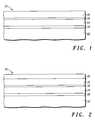
- FIGS. 1-2illustrate schematically, in cross section, device structures in accordance with various embodiments of the invention
- FIG. 3illustrates graphically the relationship between maximum attainable film thickness and lattice mismatch between a host crystal and a grown crystalline overlayer
- FIG. 4illustrates schematically, in cross-section, an exemplary embodiment of a pyroelectric detector fabricated on a semiconductor substrate according to the present invention.
- FIG. 1illustrates schematically, in cross section, a portion of a microelectronic structure 20 in accordance with an embodiment of the invention.
- Microelectronic structure 20includes a monocrystalline substrate 22 , accommodating buffer layer 24 comprising a monocrystalline material, and a layer 26 of a monocrystalline conductive oxide material.
- monocrystallineshall have the meaning commonly used within the semiconductor industry.
- the termshall refer to materials that are a single crystal or that are substantially a single crystal and shall include those materials having a relatively small number of defects such as dislocations and the like as are commonly found in substrates of silicon or germanium or mixtures of silicon and germanium and epitaxial layers of such materials commonly found in the semiconductor industry.
- structure 20also includes an amorphous intermediate layer 28 positioned between substrate 22 and accommodating buffer layer 24 .
- Structure 20may also include a template layer 30 between the accommodating buffer layer and monocrystalline oxide layer 26 .
- the template layerhelps to initiate the growth of the conductive oxide layer on the accommodating buffer layer.
- the amorphous intermediate layerhelps to relieve the strain in the accommodating buffer layer and, by doing so, aids in the growth of a high crystalline quality accommodating buffer layer.
- Substrate 22is a monocrystalline semiconductor wafer, preferably of large diameter.
- the wafercan be of a material from Group IV of the periodic table, and preferably a material from Group IVA.
- Group IV semiconductor materialsinclude silicon, germanium, mixed silicon and germanium, mixed silicon and carbon, mixed silicon, germanium and carbon, and the like.
- Substrate 22can also be of a compound semiconductor material.
- the compound semiconductor material of substrate 22can be selected, as needed for a particular semiconductor structure, from any of the Group IIIA and VA elements (III-V semiconductor compounds), mixed III-V compounds, Group II(A or B) and VIA elements (II-VI semiconductor compounds), and mixed II-VI compounds.
- Examplesinclude gallium arsenide (GaAs), gallium indium arsenide (GaInAs), gallium aluminum arsenide (GaAlAs), indium phosphide (InP), cadmium sulfide (CdS), cadmium mercury telluride (CdHgTe), zinc selenide (ZnSe), zinc sulfur selenide (ZnSSe), and the like.
- GaAsgallium arsenide
- GaInAsgallium indium arsenide
- GaAlAsgallium aluminum arsenide
- InPindium phosphide
- CdScadmium sulfide
- CdHgTecadmium mercury telluride
- ZnSezinc sulfur selenide
- ZnSSezinc sulfur selenide
- substrate 22is a wafer containing silicon or germanium, and most preferably is a high quality monocrystalline silicon wafer as used in the semiconductor industry.
- Accommodating buffer layer 24is preferably a monocrystalline oxide or nitride material epitaxially grown on the underlying substrate.
- amorphous intermediate layer 28is grown on substrate 22 at the interface between substrate 22 and the growing accommodating buffer layer by the oxidation of substrate 22 during the growth of layer 24 .
- the amorphous intermediate layerserves to relieve strain that might otherwise occur in the monocrystalline accommodating buffer layer as a result of differences in the lattice constants of the substrate and the buffer layer.
- lattice constantrefers to the distance between atoms of a cell measured in the plane of the surface. If such strain is not relieved by the amorphous intermediate layer, the strain may cause defects in the crystalline structure of the accommodating buffer layer. Defects in the crystalline structure of the accommodating buffer layer, in turn, would make it difficult to achieve a high quality crystalline structure in monocrystalline conductive oxide layer 26 .
- Accommodating buffer layer 24is preferably a monocrystalline oxide or nitride material selected for its crystalline compatibility with the underlying substrate and with the overlying conductive oxide material.
- the materialcould be an oxide or nitride having a lattice structure closely matched to the substrate and to the subsequently applied conductive oxide material.
- Materials that are suitable for the accommodating buffer layerinclude metal oxides such as the alkaline earth metal titanates, alkaline earth metal zirconates, alkaline earth metal hafnates, alkaline earth metal tantalates, alkaline earth metal ruthenates, alkaline earth metal niobates, alkaline earth metal vanadates, perovskite oxides such as alkaline earth metal tin-based perovskites, lanthanum aluminate, lanthanum scandium oxide, and gadolinium oxide. Additionally, various nitrides such as gallium nitride, aluminum nitride, and boron nitride may also be used for the accommodating buffer layer.
- metal oxidessuch as the alkaline earth metal titanates, alkaline earth metal zirconates, alkaline earth metal hafnates, alkaline earth metal tantalates, alkaline earth metal ruthenates, alkaline earth metal niobates, alkaline earth metal vanadates
- these materialsare insulators, although strontium ruthenate, for example, is a conductor.
- these materialsare metal oxides or metal nitrides, and more particularly, these metal oxide or nitrides typically include at least two different metallic elements and have a perovskite crystalline structure. In some specific applications, the metal oxides or nitride may include three or more different metallic elements.
- Amorphous interface layer 28is preferably an oxide formed by the oxidation of the surface of substrate 22 , and more preferably is composed of a silicon oxide.
- the thickness of layer 28is sufficient to relieve strain attributed to mismatches between the lattice constants of substrate 22 and accommodating buffer layer 24 .
- layer 28has a thickness in the range of approximately 0.5-5 nm.
- the conductive oxide material of layer 26can be selected, as desired for a particular structure or application.
- layer 26can include perovskite materials such as (La, Sr)CoO 3 , SrRuO 3 , SrVO 3 , BaRuO 3 , BaVO 3 and (La, Ca)MnO 3 , having a thickness in the range of about 2 to 200 nm.
- template layer 30has a thickness ranging from about 1 to about 10 monolayers.
- FIG. 2illustrates, in cross section, a portion of a microelectronic structure 40 in accordance with a further embodiment of the invention.
- Structure 40is similar to the previously described semiconductor structure 20 , except that an additional buffer layer 32 is positioned between accommodating buffer layer 24 and layer of monocrystalline layer 26 .
- the additional buffer layeris positioned between template layer 30 and the overlying layer 26 .
- the additional buffer layerserves to provide a lattice compensation when the lattice constant of the accommodating buffer layer cannot be adequately matched to the overlying monocrystalline layer.
- the additional buffer layer 32also serves as thermal insulator, blocking heat that may adversely affect an integrated circuit (described below) formed in substrate 22 .
- monocrystalline substrate 22is a silicon substrate oriented in the (100) direction.
- the silicon substratecan be, for example, a silicon substrate as is commonly used in making complementary metal oxide semiconductor (CMOS) integrated circuits having a diameter of about 200-300 mm.
- accommodating buffer layer 24is a monocrystalline layer of Sr z Ba 1 ⁇ z TiO 3 where z ranges from 0 to 1 and the amorphous intermediate layer is a layer of silicon oxide (SiO x ) formed at the interface between the silicon substrate and the accommodating buffer layer. The value of z is selected to obtain one or more lattice constants closely matched to corresponding lattice constants of the subsequently formed layer 26 .
- the accommodating buffer layercan have a thickness of about 2 to about 100 nanometers (nm) and preferably has a thickness of about 5 nm. In general, it is desired to have an accommodating buffer layer thick enough to isolate the conductive layer from the substrate to obtain the desired properties. Layers thicker than 100 nm usually provide little additional benefit while increasing cost unnecessarily; however, thicker layers may be fabricated if needed.
- the amorphous intermediate layer of silicon oxidecan have a thickness of about 0.5-5 nm, and preferably a thickness of about 1 to 2 nm.
- conductive material layer 26is a layer of (La,Sr)CoO 3 having a thickness of about 2 to about 200 nm and preferably a thickness of about 10 to about 100 nm. The thickness generally depends on the application for which the layer is being prepared.
- a template layeris formed by capping the oxide layer.
- a structureis provided that is suitable for the growth of an epitaxial film of pyroelectric material overlying a conductive material as illustrated in FIG. 2 .
- the substrateis preferably a silicon wafer as described above.
- a suitable accommodating buffer layer materialis Sr x Ba 1 ⁇ x TiO 3 , where x ranges from 0 to 1, having a thickness of about 2-100 nm and preferably a thickness of about 5-15 nm.
- the conducting oxidecan be (La, Sr)CoO 3 , having a thickness of about 2 to about 200 nm and preferably a thickness of about 10 to about 100 nm.
- a template layer to facilitate growth of an additional layer of monocrystalline materialmay be formed.
- the additional layer of monocrystalline materialcan be SrTiO 3 having a thickness of 2 to 200 nm and preferably a thickness of about 10 to 100 nm.
- a layer of pyroelectric materialmay be deposited overlying the conducting oxide layer and may include Pb(Ti, Zr)O 3 , having a thickness of about 2 to about 200 nm and preferably a thickness of about 100 to about 1000 nm.
- substrate 22is a monocrystalline substrate such as a monocrystalline silicon substrate.
- the crystalline structure of the monocrystalline substrateis characterized by a lattice constant and by a lattice orientation.
- accommodating buffer layer 24is also a monocrystalline material and the lattice of that monocrystalline material is characterized by a lattice constant and a crystal orientation.
- the lattice constants of the accommodating buffer layer and the monocrystalline substratemust be closely matched or, alternatively, must be such that upon rotation of one crystal orientation with respect to the other crystal orientation, a substantial match in lattice constants is achieved.
- the terms “substantially equal” and “substantially matched”mean that there is sufficient similarity between the lattice constants to permit the growth of a high quality crystalline layer on the underlying layer.
- FIG. 3graphically illustrates the relationship of the achievable thickness of a grown crystal layer of high crystalline quality as a function of the mismatch between the lattice constants of the host crystal and the grown crystal.
- Curve 42illustrates the boundary of high crystalline quality material. The area to the right of curve 42 represents layers that tend to be polycrystalline. With no lattice mismatch, it is theoretically possible to grow an infinitely thick, high quality epitaxial layer on the host crystal. As the mismatch in lattice constants increases, the thickness of achievable, high quality crystalline layer decreases rapidly. As a reference point, for example, if the lattice constants between the host crystal and the grown layer are mismatched by more than about 2%, monocrystalline epitaxial layers in excess of about 20 nm cannot be achieved.
- substrate 22is a (100) or (111) oriented monocrystalline silicon wafer and accommodating buffer layer 24 is a layer of strontium barium titanate.
- Substantial matching of lattice constants between these two materialsis achieved by rotating the crystal orientation of the titanate material by 45° with respect to the crystal orientation of the silicon substrate wafer.
- the inclusion in the structure of amorphous interface layer 28a silicon oxide layer in this example, if it is of sufficient thickness, serves to reduce strain in the titanate monocrystalline layer that might result from any mismatch in the lattice constants of the host silicon wafer and the grown titanate layer.
- a high quality, thick, monocrystalline titanate layeris achievable.
- layer 26is a layer of epitaxially grown conductive oxide material and that crystalline material is also characterized by a crystal lattice constant and a crystal orientation.
- the lattice constant of layer 26differs from the lattice constant of substrate 22 .
- the accommodating buffer layermust be of high crystalline quality.
- substantial matching between the crystal lattice constant of the host crystal, in this case, the monocrystalline accommodating buffer layer, and the grown crystalis desired.
- a crystalline buffer layer between the host oxide and the grown conductive oxide layercan be used to reduce strain in the grown monocrystalline conductive oxide layer that might result from small differences in lattice constants. Better crystalline quality in the grown monocrystalline conductive oxide layer can thereby be achieved.
- the following exampleillustrates a process, in accordance with one embodiment of the invention, for fabricating a microelectronic structure such as the structures depicted in FIGS. 1-2.
- the processstarts by providing a monocrystalline semiconductor substrate comprising silicon or germanium.
- the semiconductor substrateis a silicon wafer having a (100) orientation.
- the substrateis preferably oriented on axis or, at most, about 4° off axis.
- At least a portion of the semiconductor substratehas a bare surface, although other portions of the substrate, as described below, may encompass other structures.
- the term “bare” in this contextmeans that the surface in the portion of the substrate has been cleaned to remove any oxides, contaminants, or other foreign material.
- bare siliconis highly reactive and readily forms a native oxide.
- the term “bare”is intended to encompass such a native oxide.
- a thin silicon oxidemay also be intentionally grown on the semiconductor substrate, although such a grown oxide is not essential to the process in accordance with the invention.
- the native oxide layerIn order to epitaxially grow a monocrystalline oxide layer overlying the monocrystalline substrate, the native oxide layer must first be removed to expose the crystalline structure of the underlying substrate. The following process is preferably carried out by molecular beam epitaxy (MBE), although other epitaxial processes may also be used in accordance with the present invention.
- MBEmolecular beam epitaxy
- the native oxidecan be removed by first thermally depositing a thin layer of strontium, barium, a combination of strontium and barium, or other alkali earth metals or combinations of alkali earth metals in an MBE apparatus.
- the substrateis then heated to a temperature of about 850° C. to cause the strontium to react with the native silicon oxide layer.
- the strontiumserves to reduce the silicon oxide to leave a silicon oxide-free surface.
- the resultant surfacewhich exhibits an ordered 2 ⁇ 1 structure, includes strontium, oxygen, and silicon.
- the ordered 2 ⁇ 1 structureforms a template for the ordered growth of an overlying layer of a monocrystalline oxide.
- the templateprovides the necessary chemical and physical properties to nucleate the crystalline growth of an overlying layer.
- the native silicon oxidecan be converted and the substrate surface can be prepared for the growth of a monocrystalline oxide layer by depositing an alkali earth metal oxide, such as strontium oxide, strontium barium oxide, or barium oxide, onto the substrate surface by MBE at a low temperature and by subsequently heating the structure to a temperature of about 850° C. At this temperature, a solid state reaction takes place between the strontium oxide and the native silicon oxide, causing the reduction of the native silicon oxide and leaving an ordered 2 ⁇ 1 structure with strontium, oxygen, and silicon remaining on the substrate surface. Again, this forms a template for the subsequent growth of an ordered monocrystalline oxide layer.
- an alkali earth metal oxidesuch as strontium oxide, strontium barium oxide, or barium oxide
- the substrateis cooled to a temperature in the range of about 200-800° C. and a layer of strontium titanate is grown on the template layer by molecular beam epitaxy.
- the MBE processis initiated by opening shutters in the MBE apparatus to expose strontium, titanium and oxygen sources.
- the ratio of strontium and titaniumis approximately 1:1.
- the partial pressure of oxygenis initially set at a minimum value to grow stoichiometric strontium titanate at a growth rate of about 0.3-0.5 nm per minute. After initiating growth of the strontium titanate, the partial pressure of oxygen is increased above the initial minimum value.
- the overpressure of oxygencauses the growth of an amorphous silicon oxide layer at the interface between the underlying substrate and the growing strontium titanate layer.
- the growth of the silicon oxide layerresults from the diffusion of oxygen through the growing strontium titanate layer to the interface where the oxygen reacts with silicon at the surface of the underlying substrate.
- the strontium titanategrows as an ordered monocrystal with the crystalline orientation rotated by 45° with respect to the ordered 2 ⁇ 1 crystalline structure of the underlying substrate. Strain that otherwise might exist in the strontium titanate layer because of the small mismatch in lattice constant between the silicon substrate and the growing crystal is relieved in the amorphous silicon oxide intermediate layer.
- the monocrystalline strontium titanatemay be capped by a template layer that is conducive to the subsequent growth of an epitaxial layer of a desired conductive oxide material.
- the MBE growth of the strontium titanate monocrystalline layercan be capped by terminating the growth with 1-2 monolayers of titanium, 1-2 monolayers of titanium-oxygen or with 1-2 monolayers of strontium-oxygen.
- the conductive oxide materialis grown using MBE or other suitable techniques.
- the process described aboveillustrates a process for forming a semiconductor structure including a silicon substrate, an overlying oxide layer, and a monocrystalline conductive oxide layer by the process of molecular beam epitaxy.
- the processcan also be carried out by the process of chemical vapor deposition (CVD), metal organic chemical vapor deposition (MOCVD), migration enhanced epitaxy (MEE), atomic layer epitaxy (ALE), physical vapor deposition (PVD), chemical solution deposition (CSD), pulsed laser deposition (PLD), or the like.
- CVDchemical vapor deposition
- MOCVDmetal organic chemical vapor deposition
- MEEmigration enhanced epitaxy
- ALEatomic layer epitaxy
- PVDphysical vapor deposition
- CSSDchemical solution deposition
- PLDpulsed laser deposition
- monocrystalline accommodating buffer layerssuch as alkaline earth metal titanates, zirconates, hafnates, tantalates, vanadates, ruthenates, and niobates, perovskite oxides such as alkaline earth metal tin-based perovskites, lanthanum aluminate, lanthanum scandium oxide, and gadolinium oxide can also be grown.
- perovskite oxidessuch as alkaline earth metal tin-based perovskites, lanthanum aluminate, lanthanum scandium oxide, and gadolinium oxide
- MBEother conductive oxide layers can be deposited overlying the monocrystalline oxide accommodating buffer layer.
- Each of the variations of conductive oxide layers, pyroelectric layers, and monocrystalline oxide accommodating buffer layersmay use an appropriate template for initiating the growth of the respective layer.
- suitable template materialsmay be grown according to the methods described above in connection with growing layer 26 .
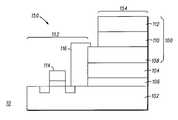
- FIG. 4illustrates a device structure 150 in accordance with a further embodiment of the present invention.
- Structure 150includes a first region 152 in which an electrical component 114 is formed within a substrate 102 and a second region 154 in which a pyroelectric element 100 is formed using a pyroelectric layer 110 .
- a monocrystalline substrate 102such as silicon functions as the starting material.
- a monocrystalline perovskite accommodating buffer layer 104is then grown epitaxially over substrate 102 and an amorphous intermediate layer 106 may be formed between substrate 102 and layer 104 by the oxidation of substrate 102 during the growth of layer 104 .
- Element 100is similar to structure 20 , except that a template layer is not illustrated in FIG. 4 .
- element 100may include a template layer between any adjacent monocrystalline layers as described herein.
- substrate 102is a silicon substrate
- layer 104is an insulative oxide layer of perovskite, as discussed above in connection with layer 24 , illustrated in FIGS. 1-2 above.
- layer 104may be formed from material from the group which includes, but is not limited to, BaTiO 3 , SrTiO 3 , and CaTiO 3 and may have a thickness in the range of about 2-100 nm.
- Conducting layer 108behaves as either a metallic conductor or a semiconductor.
- conducting layer 108is a monocrystalline perovskite oxide material.
- Exemplary materials suitable for forming conducting layer 108include, but are not limited to, (La, Sr)CoO 3 , SrRuO 3 , SrVO 3 , BaRuO 3 , BaVO 3 , and (La, Ca)MnO 3 .
- Conducting layer 108preferably exhibits a thickness in the range of about 2 nm to 200 nm.
- a pyroelectric layer 110is deposited on conducting layer 108 .
- Exemplary pyroelectric materials suitable for pyroelectric layer 110include perovskite metallic oxides such as Pb(Ti, Zr)O 3 , PbTiO 3 , BaTiO 3 , Pb(Sc, Ta)O 3 , Bi(Ti, Zr) 3 O 12 , SrBi 2 (Ta, Nb) 2 O 9 , and YMnO 3 .
- Pyroelectric layer 110preferably exhibits a thickness in the range of about 2 to 200 nm.
- Electrode layer 112is formed overlying pyroelectric layer 110 .
- Electrode layer 112can be formed of any suitable conductive material such as Ni, Cr, Pt, Ir, Ti and the like and preferably absorbs infrared radiation of a wavelength in the range of about 8 ⁇ m to 12 ⁇ m.
- electrode layer 112may also be formed of a monocrystalline perovskite conducting oxide, such as those materials used to form conducting layer 108 , for example, (La, Sr)CoO 3 .
- Pyroelectric element 100is coupled to a CMOS device 114 via a suitable interconnect 116 to form a pyroelectric imaging device, such as those used for motion detection or thermal imaging.
- CMOS device 114may comprise a device such as a MOSFET which is formed by conventional semiconductor processing as is well known and widely practiced in the semiconductor industry.
- a metal layer(not shown) may be deposited overlying conducting layer 108 before pyroelectric layer 110 is deposited thereon.
- a plurality of pyroelectric imaging devices which detect the same or different wavelengths of infrared radiationmay then be combined in an array which produces an image corresponding to the received infrared radiation.
- a portion of substrate 102is preferably removed proximate pyroelectric element 100 .
- the portion of substrate 102is removed using an etch which selectively etches material of substrate 102 relative to material comprising layer 104 , that is, layer 104 may serve as an etch-stop.
- layer 104may serve as a thermal insulating layer, thereby thermally isolating substrate 102 from the pyroelectric layer 110 and reducing the thermal conduction of substrate 102 . Accordingly, it may not be necessary to remove a portion of substrate 102 proximate pyroelectric element 100 .
- a thermal insulation layersuch as BaTiO 3 , SrTiO 3 and CaTiO 3 may be epitaxially grown on accommodating buffer layer 104 before the formation of conduction layer 108 .
- the thermal insulation layerwould serve to thermally insulate substrate 102 , thereby rendering the selective etching of substrate 102 proximate to the pyroelectric device unnecessary.
- steps of epitaxially growing or depositing the various layersincludes epitaxially growing or depositing layers by processes such as MBE, MOCVD, MEE, CVD, PVD, CSD and ALE as previously indicated with respect to the processing steps described above for fabricating the structures shown in FIGS. 1-3.
Landscapes
- Chemical & Material Sciences (AREA)
- Metallurgy (AREA)
- Engineering & Computer Science (AREA)
- Crystallography & Structural Chemistry (AREA)
- Materials Engineering (AREA)
- Organic Chemistry (AREA)
- General Chemical & Material Sciences (AREA)
- Chemical Kinetics & Catalysis (AREA)
- Inorganic Chemistry (AREA)
- Photometry And Measurement Of Optical Pulse Characteristics (AREA)
- Semiconductor Memories (AREA)
- Recrystallisation Techniques (AREA)
- Crystals, And After-Treatments Of Crystals (AREA)
Abstract
Description
Claims (6)
Priority Applications (3)
| Application Number | Priority Date | Filing Date | Title |
|---|---|---|---|
| US09/733,181US6563118B2 (en) | 2000-12-08 | 2000-12-08 | Pyroelectric device on a monocrystalline semiconductor substrate and process for fabricating same |
| AU2002227030AAU2002227030A1 (en) | 2000-12-08 | 2001-11-29 | Pyroelectric device on a monocrystalline semiconductor substrate |
| PCT/US2001/044776WO2002047127A2 (en) | 2000-12-08 | 2001-11-29 | Pyroelectric device on a monocrystalline semiconductor substrate |
Applications Claiming Priority (1)
| Application Number | Priority Date | Filing Date | Title |
|---|---|---|---|
| US09/733,181US6563118B2 (en) | 2000-12-08 | 2000-12-08 | Pyroelectric device on a monocrystalline semiconductor substrate and process for fabricating same |
Publications (2)
| Publication Number | Publication Date |
|---|---|
| US20020072245A1 US20020072245A1 (en) | 2002-06-13 |
| US6563118B2true US6563118B2 (en) | 2003-05-13 |
Family
ID=24946567
Family Applications (1)
| Application Number | Title | Priority Date | Filing Date |
|---|---|---|---|
| US09/733,181Expired - Fee RelatedUS6563118B2 (en) | 2000-12-08 | 2000-12-08 | Pyroelectric device on a monocrystalline semiconductor substrate and process for fabricating same |
Country Status (3)
| Country | Link |
|---|---|
| US (1) | US6563118B2 (en) |
| AU (1) | AU2002227030A1 (en) |
| WO (1) | WO2002047127A2 (en) |
Cited By (8)
| Publication number | Priority date | Publication date | Assignee | Title |
|---|---|---|---|---|
| US20030168000A1 (en)* | 2002-03-06 | 2003-09-11 | Jun Amano | Lead-based perovskite buffer for forming indium phosphide on silicon |
| US20030218644A1 (en)* | 2002-03-25 | 2003-11-27 | Takamitsu Higuchi | Board for electronic device, electronic device, ferroelectric memory, electronic apparatus, ink-jet recording head, and ink-jet printer |
| US20040043548A1 (en)* | 2002-08-27 | 2004-03-04 | Redd Randy D. | Method for forming a semiconductor device |
| US20040253746A1 (en)* | 2003-06-10 | 2004-12-16 | Nec Electronics Corporation | Semiconductor storage device and method of manufacturing the same |
| GB2411521A (en)* | 2004-02-27 | 2005-08-31 | Qinetiq Ltd | Fabrication method for micro-sensor device |
| US20060011129A1 (en)* | 2004-07-14 | 2006-01-19 | Atomic Energy Council - Institute Of Nuclear Energy Research | Method for fabricating a compound semiconductor epitaxial wafer |
| US20110114968A1 (en)* | 2003-03-03 | 2011-05-19 | Sheppard Scott T | Integrated Nitride and Silicon Carbide-Based Devices |
| US20110280276A1 (en)* | 2010-05-06 | 2011-11-17 | Commissariat A L'energie Atomique Et Aux Energies Alternatives | Time-related temperature variation transducer, electronic chip incorporating this transducer and method of fabrication of this chip |
Families Citing this family (32)
| Publication number | Priority date | Publication date | Assignee | Title |
|---|---|---|---|---|
| US6392257B1 (en) | 2000-02-10 | 2002-05-21 | Motorola Inc. | Semiconductor structure, semiconductor device, communicating device, integrated circuit, and process for fabricating the same |
| US6693033B2 (en) | 2000-02-10 | 2004-02-17 | Motorola, Inc. | Method of removing an amorphous oxide from a monocrystalline surface |
| JP2004503920A (en) | 2000-05-31 | 2004-02-05 | モトローラ・インコーポレイテッド | Semiconductor device and method of manufacturing the semiconductor device |
| AU2001264987A1 (en)* | 2000-06-30 | 2002-01-14 | Motorola, Inc., A Corporation Of The State Of Delware | Hybrid semiconductor structure and device |
| WO2002009187A2 (en) | 2000-07-24 | 2002-01-31 | Motorola, Inc. | Heterojunction tunneling diodes and process for fabricating same |
| US6555946B1 (en) | 2000-07-24 | 2003-04-29 | Motorola, Inc. | Acoustic wave device and process for forming the same |
| US6638838B1 (en) | 2000-10-02 | 2003-10-28 | Motorola, Inc. | Semiconductor structure including a partially annealed layer and method of forming the same |
| US6583034B2 (en) | 2000-11-22 | 2003-06-24 | Motorola, Inc. | Semiconductor structure including a compliant substrate having a graded monocrystalline layer and methods for fabricating the structure and semiconductor devices including the structure |
| US20020096683A1 (en)* | 2001-01-19 | 2002-07-25 | Motorola, Inc. | Structure and method for fabricating GaN devices utilizing the formation of a compliant substrate |
| US6673646B2 (en) | 2001-02-28 | 2004-01-06 | Motorola, Inc. | Growth of compound semiconductor structures on patterned oxide films and process for fabricating same |
| WO2002082551A1 (en) | 2001-04-02 | 2002-10-17 | Motorola, Inc. | A semiconductor structure exhibiting reduced leakage current |
| US6709989B2 (en) | 2001-06-21 | 2004-03-23 | Motorola, Inc. | Method for fabricating a semiconductor structure including a metal oxide interface with silicon |
| US6992321B2 (en)* | 2001-07-13 | 2006-01-31 | Motorola, Inc. | Structure and method for fabricating semiconductor structures and devices utilizing piezoelectric materials |
| US6646293B2 (en) | 2001-07-18 | 2003-11-11 | Motorola, Inc. | Structure for fabricating high electron mobility transistors utilizing the formation of complaint substrates |
| US6693298B2 (en) | 2001-07-20 | 2004-02-17 | Motorola, Inc. | Structure and method for fabricating epitaxial semiconductor on insulator (SOI) structures and devices utilizing the formation of a compliant substrate for materials used to form same |
| US7019332B2 (en) | 2001-07-20 | 2006-03-28 | Freescale Semiconductor, Inc. | Fabrication of a wavelength locker within a semiconductor structure |
| US6855992B2 (en) | 2001-07-24 | 2005-02-15 | Motorola Inc. | Structure and method for fabricating configurable transistor devices utilizing the formation of a compliant substrate for materials used to form the same |
| US6667196B2 (en) | 2001-07-25 | 2003-12-23 | Motorola, Inc. | Method for real-time monitoring and controlling perovskite oxide film growth and semiconductor structure formed using the method |
| US6589856B2 (en) | 2001-08-06 | 2003-07-08 | Motorola, Inc. | Method and apparatus for controlling anti-phase domains in semiconductor structures and devices |
| US6639249B2 (en) | 2001-08-06 | 2003-10-28 | Motorola, Inc. | Structure and method for fabrication for a solid-state lighting device |
| US20030034491A1 (en) | 2001-08-14 | 2003-02-20 | Motorola, Inc. | Structure and method for fabricating semiconductor structures and devices for detecting an object |
| US6673667B2 (en) | 2001-08-15 | 2004-01-06 | Motorola, Inc. | Method for manufacturing a substantially integral monolithic apparatus including a plurality of semiconductor materials |
| US20030071327A1 (en) | 2001-10-17 | 2003-04-17 | Motorola, Inc. | Method and apparatus utilizing monocrystalline insulator |
| US6607969B1 (en)* | 2002-03-18 | 2003-08-19 | The United States Of America As Represented By The Secretary Of The Navy | Method for making pyroelectric, electro-optical and decoupling capacitors using thin film transfer and hydrogen ion splitting techniques |
| US6916717B2 (en) | 2002-05-03 | 2005-07-12 | Motorola, Inc. | Method for growing a monocrystalline oxide layer and for fabricating a semiconductor device on a monocrystalline substrate |
| US7169619B2 (en) | 2002-11-19 | 2007-01-30 | Freescale Semiconductor, Inc. | Method for fabricating semiconductor structures on vicinal substrates using a low temperature, low pressure, alkaline earth metal-rich process |
| US6885065B2 (en) | 2002-11-20 | 2005-04-26 | Freescale Semiconductor, Inc. | Ferromagnetic semiconductor structure and method for forming the same |
| US7020374B2 (en) | 2003-02-03 | 2006-03-28 | Freescale Semiconductor, Inc. | Optical waveguide structure and method for fabricating the same |
| US6965128B2 (en) | 2003-02-03 | 2005-11-15 | Freescale Semiconductor, Inc. | Structure and method for fabricating semiconductor microresonator devices |
| DE10352655A1 (en)* | 2003-11-11 | 2005-06-30 | Universität Augsburg | Heteroepitaxial layer and process for its preparation |
| US8208284B2 (en)* | 2008-03-07 | 2012-06-26 | Unity Semiconductor Corporation | Data retention structure for non-volatile memory |
| CN111926295B (en)* | 2020-09-01 | 2022-08-09 | 深圳大学 | Huge tetragonal phase PbTiO 3 Method for producing thin film |
Citations (132)
| Publication number | Priority date | Publication date | Assignee | Title |
|---|---|---|---|---|
| GB1319311A (en) | 1970-06-04 | 1973-06-06 | North American Rockwell | Epitaxial composite and method of making |
| US3766370A (en) | 1971-05-14 | 1973-10-16 | Hewlett Packard Co | Elementary floating point cordic function processor and shifter |
| US3802967A (en) | 1971-08-27 | 1974-04-09 | Rca Corp | Iii-v compound on insulating substrate and its preparation and use |
| US4006989A (en) | 1972-10-02 | 1977-02-08 | Raytheon Company | Laser gyroscope |
| US4174422A (en) | 1977-12-30 | 1979-11-13 | International Business Machines Corporation | Growing epitaxial films when the misfit between film and substrate is large |
| US4284329A (en) | 1978-01-03 | 1981-08-18 | Raytheon Company | Laser gyroscope system |
| US4404265A (en) | 1969-10-01 | 1983-09-13 | Rockwell International Corporation | Epitaxial composite and method of making |
| US4482906A (en) | 1982-06-30 | 1984-11-13 | International Business Machines Corporation | Gallium aluminum arsenide integrated circuit structure using germanium |
| US4484332A (en) | 1982-06-02 | 1984-11-20 | The United States Of America As Represented By The Secretary Of The Air Force | Multiple double heterojunction buried laser device |
| US4523211A (en) | 1982-03-16 | 1985-06-11 | Futaba Denshi Kogyo Kabushiki Kaisha | Semiconductor device |
| JPS61108187A (en) | 1984-11-01 | 1986-05-26 | Seiko Epson Corp | Semiconductor optoelectronic device |
| US4661176A (en) | 1985-02-27 | 1987-04-28 | The United States Of America As Represented By The Secretary Of The Air Force | Process for improving the quality of epitaxial silicon films grown on insulating substrates utilizing oxygen ion conductor substrates |
| JPS62216600A (en) | 1986-03-18 | 1987-09-24 | Oki Electric Ind Co Ltd | Photo-acoustic transducing device |
| JPS6334994A (en) | 1986-07-29 | 1988-02-15 | Mitsubishi Electric Corp | Photoelectric integrated circuit device and manufacture thereof |
| JPS63131104A (en) | 1986-11-20 | 1988-06-03 | Nippon Telegr & Teleph Corp <Ntt> | Hybrid optical integrated circuit |
| US4777613A (en) | 1986-04-01 | 1988-10-11 | Motorola Inc. | Floating point numeric data processor |
| US4793872A (en) | 1986-03-07 | 1988-12-27 | Thomson-Csf | III-V Compound heteroepitaxial 3-D semiconductor structures utilizing superlattices |
| US4802182A (en) | 1987-11-05 | 1989-01-31 | Xerox Corporation | Monolithic two dimensional waveguide coupled cavity laser/modulator |
| US4815084A (en) | 1987-05-20 | 1989-03-21 | Spectra Diode Laboratories, Inc. | Semiconductor laser with integrated optical elements |
| US4846926A (en) | 1985-08-26 | 1989-07-11 | Ford Aerospace & Communications Corporation | HcCdTe epitaxially grown on crystalline support |
| US4855249A (en) | 1985-11-18 | 1989-08-08 | Nagoya University | Process for growing III-V compound semiconductors on sapphire using a buffer layer |
| US4876219A (en) | 1988-03-04 | 1989-10-24 | Fujitsu Limited | Method of forming a heteroepitaxial semiconductor thin film using amorphous buffer layers |
| US4882300A (en) | 1987-10-12 | 1989-11-21 | Agency Of Industrial Science And Technology | Method of forming single crystalline magnesia spinel film |
| US4891091A (en) | 1986-07-14 | 1990-01-02 | Gte Laboratories Incorporated | Method of epitaxially growing compound semiconductor materials |
| US4896194A (en) | 1987-07-08 | 1990-01-23 | Nec Corporation | Semiconductor device having an integrated circuit formed on a compound semiconductor layer |
| US4912087A (en) | 1988-04-15 | 1990-03-27 | Ford Motor Company | Rapid thermal annealing of superconducting oxide precursor films on Si and SiO2 substrates |
| US4928154A (en) | 1985-09-03 | 1990-05-22 | Daido Tokushuko Kabushiki Kaisha | Epitaxial gallium arsenide semiconductor on silicon substrate with gallium phosphide and superlattice intermediate layers |
| US4963949A (en) | 1988-09-30 | 1990-10-16 | The United States Of America As Represented Of The United States Department Of Energy | Substrate structures for InP-based devices |
| JPH02306680A (en) | 1989-05-22 | 1990-12-20 | Hikari Gijutsu Kenkyu Kaihatsu Kk | Optoelectronic integrated circuit device and manufacture thereof |
| US4999842A (en) | 1989-03-01 | 1991-03-12 | At&T Bell Laboratories | Quantum well vertical cavity laser |
| US5060031A (en) | 1990-09-18 | 1991-10-22 | Motorola, Inc | Complementary heterojunction field effect transistor with an anisotype N+ ga-channel devices |
| US5063166A (en) | 1988-04-29 | 1991-11-05 | Sri International | Method of forming a low dislocation density semiconductor device |
| EP0455526A1 (en) | 1990-04-13 | 1991-11-06 | Thomson-Csf | Process for adaptation between two crystallized semiconductor materials, and semiconductor device |
| US5081062A (en) | 1987-08-27 | 1992-01-14 | Prahalad Vasudev | Monolithic integration of silicon on insulator and gallium arsenide semiconductor technologies |
| US5116461A (en) | 1991-04-22 | 1992-05-26 | Motorola, Inc. | Method for fabricating an angled diffraction grating |
| US5127067A (en) | 1990-09-10 | 1992-06-30 | Westinghouse Electric Corp. | Local area network with star topology and ring protocol |
| US5141894A (en) | 1989-08-01 | 1992-08-25 | Thomson-Csf | Method for the manufacture, by epitaxy, of monocrystalline layers of materials with different lattice parameters |
| US5144409A (en) | 1990-09-05 | 1992-09-01 | Yale University | Isotopically enriched semiconductor devices |
| US5155658A (en) | 1992-03-05 | 1992-10-13 | Bell Communications Research, Inc. | Crystallographically aligned ferroelectric films usable in memories and method of crystallographically aligning perovskite films |
| US5159413A (en) | 1990-04-20 | 1992-10-27 | Eaton Corporation | Monolithic integrated circuit having compound semiconductor layer epitaxially grown on ceramic substrate |
| EP0250171B1 (en) | 1986-06-13 | 1992-11-11 | Massachusetts Institute Of Technology | Compound semiconductor devices |
| EP0514018A2 (en) | 1991-04-24 | 1992-11-19 | AT&T Corp. | Method for making low defect density semiconductor heterostructure and devices made thereby |
| US5173474A (en) | 1990-04-18 | 1992-12-22 | Xerox Corporation | Silicon substrate having an epitaxial superconducting layer thereon and method of making same |
| JPH0548072A (en) | 1991-08-12 | 1993-02-26 | Nippon Telegr & Teleph Corp <Ntt> | Semiconductor element |
| US5221367A (en) | 1988-08-03 | 1993-06-22 | International Business Machines, Corp. | Strained defect-free epitaxial mismatched heterostructures and method of fabrication |
| US5225031A (en) | 1991-04-10 | 1993-07-06 | Martin Marietta Energy Systems, Inc. | Process for depositing an oxide epitaxially onto a silicon substrate and structures prepared with the process |
| US5248564A (en)* | 1992-12-09 | 1993-09-28 | Bell Communications Research, Inc. | C-axis perovskite thin films grown on silicon dioxide |
| US5270298A (en) | 1992-03-05 | 1993-12-14 | Bell Communications Research, Inc. | Cubic metal oxide thin film epitaxially grown on silicon |
| US5286985A (en) | 1988-11-04 | 1994-02-15 | Texas Instruments Incorporated | Interface circuit operable to perform level shifting between a first type of device and a second type of device |
| US5293050A (en) | 1993-03-25 | 1994-03-08 | International Business Machines Corporation | Semiconductor quantum dot light emitting/detecting devices |
| US5310707A (en) | 1990-03-28 | 1994-05-10 | Superconductivity Research Laboratory International | Substrate material for the preparation of oxide superconductors |
| US5326721A (en) | 1992-05-01 | 1994-07-05 | Texas Instruments Incorporated | Method of fabricating high-dielectric constant oxides on semiconductors using a GE buffer layer |
| EP0342937B1 (en) | 1988-05-17 | 1994-07-27 | Fujitsu Limited | Manufacturing a semiconductor wafer having a III-V group semiconductor compound layer on a silicon substrate |
| US5358925A (en) | 1990-04-18 | 1994-10-25 | Board Of Trustees Of The Leland Stanford Junior University | Silicon substrate having YSZ epitaxial barrier layer and an epitaxial superconducting layer |
| EP0602568A3 (en) | 1992-12-17 | 1994-12-28 | Eastman Kodak Co | A multilayer structure having a (111)-oriented buffer layer. |
| US5391515A (en) | 1988-10-28 | 1995-02-21 | Texas Instruments Incorporated | Capped anneal |
| US5393352A (en) | 1992-05-01 | 1995-02-28 | Texas Instruments Incorporated | Pb/Bi-containing high-dielectric constant oxides using a non-P/Bi-containing perovskite as a buffer layer |
| US5404581A (en) | 1991-07-25 | 1995-04-04 | Nec Corporation | Microwave . millimeter wave transmitting and receiving module |
| US5418216A (en) | 1990-11-30 | 1995-05-23 | Fork; David K. | Superconducting thin films on epitaxial magnesium oxide grown on silicon |
| US5418389A (en) | 1992-11-09 | 1995-05-23 | Mitsubishi Chemical Corporation | Field-effect transistor with perovskite oxide channel |
| US5436759A (en) | 1994-06-14 | 1995-07-25 | The Regents Of The University Of California | Cross-talk free, low-noise optical amplifier |
| US5442191A (en) | 1990-09-05 | 1995-08-15 | Yale University | Isotopically enriched semiconductor devices |
| US5444016A (en) | 1993-06-25 | 1995-08-22 | Abrokwah; Jonathan K. | Method of making ohmic contacts to a complementary III-V semiconductor device |
| US5450812A (en) | 1993-07-30 | 1995-09-19 | Martin Marietta Energy Systems, Inc. | Process for growing a film epitaxially upon an oxide surface and structures formed with the process |
| US5478653A (en) | 1994-04-04 | 1995-12-26 | Guenzer; Charles S. | Bismuth titanate as a template layer for growth of crystallographically oriented silicon |
| US5480829A (en) | 1993-06-25 | 1996-01-02 | Motorola, Inc. | Method of making a III-V complementary heterostructure device with compatible non-gold ohmic contacts |
| US5482003A (en) | 1991-04-10 | 1996-01-09 | Martin Marietta Energy Systems, Inc. | Process for depositing epitaxial alkaline earth oxide onto a substrate and structures prepared with the process |
| US5514484A (en) | 1992-11-05 | 1996-05-07 | Fuji Xerox Co., Ltd. | Oriented ferroelectric thin film |
| US5528414A (en) | 1994-05-05 | 1996-06-18 | Lots Technology | Two dimensional electro-optic modulator array |
| US5576879A (en) | 1994-01-14 | 1996-11-19 | Fuji Xerox Co., Ltd. | Composite optical modulator |
| US5588995A (en) | 1993-06-01 | 1996-12-31 | Midwest Research Institute | System for monitoring the growth of crystalline films on stationary substrates |
| US5606184A (en) | 1995-05-04 | 1997-02-25 | Motorola, Inc. | Heterostructure field effect device having refractory ohmic contact directly on channel layer and method for making |
| US5614739A (en) | 1995-06-02 | 1997-03-25 | Motorola | HIGFET and method |
| US5640267A (en) | 1994-03-02 | 1997-06-17 | Sharp Kabushiki Kaisha | Optical apparatus |
| US5670798A (en) | 1995-03-29 | 1997-09-23 | North Carolina State University | Integrated heterostructures of Group III-V nitride semiconductor materials including epitaxial ohmic contact non-nitride buffer layer and methods of fabricating same |
| US5674366A (en) | 1992-12-01 | 1997-10-07 | Matsushita Electric Industrial Co., Ltd. | Method and apparatus for fabrication of dielectric thin film |
| US5729641A (en) | 1996-05-30 | 1998-03-17 | Sdl, Inc. | Optical device employing edge-coupled waveguide geometry |
| US5729394A (en) | 1996-01-24 | 1998-03-17 | Hewlett-Packard Company | Multi-direction optical data port |
| US5731220A (en) | 1994-09-30 | 1998-03-24 | Texas Instruments Incorporated | Method of making barium strontium titanate (BST) thin film by erbium donor doping |
| US5733641A (en) | 1996-05-31 | 1998-03-31 | Xerox Corporation | Buffered substrate for semiconductor devices |
| US5735949A (en) | 1990-09-13 | 1998-04-07 | Forschungszentrum Julich Gmbh | Method of producing electronic, electrooptical and optical components |
| US5741724A (en) | 1996-12-27 | 1998-04-21 | Motorola | Method of growing gallium nitride on a spinel substrate |
| US5764676A (en) | 1996-09-26 | 1998-06-09 | Xerox Corporation | Transversely injected multiple wavelength diode laser array formed by layer disordering |
| US5778018A (en) | 1994-10-13 | 1998-07-07 | Nec Corporation | VCSELs (vertical-cavity surface emitting lasers) and VCSEL-based devices |
| US5777762A (en) | 1995-06-06 | 1998-07-07 | Canon Kabushiki Kaisha | Network system for performing bidirectional transmission, and node device and transmission control method used in the system |
| US5778116A (en) | 1997-01-23 | 1998-07-07 | Tomich; John L. | Photonic home area network fiber/power insertion apparatus |
| US5790583A (en) | 1995-05-25 | 1998-08-04 | Northwestern University | Photonic-well Microcavity light emitting devices |
| US5801105A (en) | 1995-08-04 | 1998-09-01 | Tdk Corporation | Multilayer thin film, substrate for electronic device, electronic device, and preparation of multilayer oxide thin film |
| US5810923A (en) | 1994-08-17 | 1998-09-22 | Tdk Corporation | Method for forming oxide thin film and the treatment of silicon substrate |
| US5825799A (en) | 1995-05-25 | 1998-10-20 | Northwestern University | Microcavity semiconductor laser |
| US5830270A (en) | 1996-08-05 | 1998-11-03 | Lockheed Martin Energy Systems, Inc. | CaTiO3 Interfacial template structure on semiconductor-based material and the growth of electroceramic thin-films in the perovskite class |
| US5857049A (en) | 1997-05-05 | 1999-01-05 | Lucent Technologies, Inc., | Precision alignment of optoelectronic devices |
| US5858814A (en) | 1996-07-17 | 1999-01-12 | Lucent Technologies Inc. | Hybrid chip and method therefor |
| US5861966A (en) | 1995-12-27 | 1999-01-19 | Nynex Science & Technology, Inc. | Broad band optical fiber telecommunications network |
| US5874860A (en) | 1996-02-06 | 1999-02-23 | Motorola, Inc. | High frequency amplifier and control |
| US5883996A (en) | 1995-09-29 | 1999-03-16 | Motorola, Inc. | Electronic component for aligning a light transmitting structure |
| US5912068A (en) | 1996-12-05 | 1999-06-15 | The Regents Of The University Of California | Epitaxial oxides on amorphous SiO2 on single crystal silicon |
| US5926496A (en) | 1995-05-25 | 1999-07-20 | Northwestern University | Semiconductor micro-resonator device |
| US5937285A (en) | 1997-05-23 | 1999-08-10 | Motorola, Inc. | Method of fabricating submicron FETs with low temperature group III-V material |
| JPH11260835A (en) | 1997-07-11 | 1999-09-24 | Tdk Corp | Substrates for electronic devices |
| EP0607435B1 (en) | 1992-08-07 | 1999-11-03 | Asahi Kasei Kogyo Kabushiki Kaisha | Nitride based semiconductor device and manufacture thereof |
| US5981400A (en) | 1997-09-18 | 1999-11-09 | Cornell Research Foundation, Inc. | Compliant universal substrate for epitaxial growth |
| US5990495A (en) | 1995-08-25 | 1999-11-23 | Kabushiki Kaisha Toshiba | Semiconductor light-emitting element and method for manufacturing the same |
| US5995359A (en) | 1994-06-18 | 1999-11-30 | U.S. Philips Corporation | Electronic component and method of manufacturing same |
| US6002375A (en) | 1997-09-02 | 1999-12-14 | Motorola, Inc. | Multi-substrate radio-frequency circuit |
| US6008762A (en) | 1997-03-31 | 1999-12-28 | Qualcomm Incorporated | Folded quarter-wave patch antenna |
| US6020222A (en) | 1997-12-16 | 2000-02-01 | Advanced Micro Devices, Inc. | Silicon oxide insulator (SOI) semiconductor having selectively linked body |
| US6055179A (en) | 1998-05-19 | 2000-04-25 | Canon Kk | Memory device utilizing giant magnetoresistance effect |
| US6058131A (en) | 1997-11-17 | 2000-05-02 | E-Tek Dynamics, Inc. | Wavelength stabilization of laser source using fiber Bragg grating feedback |
| EP0999600A2 (en) | 1998-11-03 | 2000-05-10 | Lockheed Martin Corporation | Multi-band infrared photodetector |
| US6064078A (en) | 1998-05-22 | 2000-05-16 | Xerox Corporation | Formation of group III-V nitride films on sapphire substrates with reduced dislocation densities |
| US6064092A (en) | 1995-06-13 | 2000-05-16 | Samsung Electronics Co., Ltd. | Semiconductor-on-insulator substrates containing electrically insulating mesas |
| EP1001468A1 (en) | 1998-11-12 | 2000-05-17 | Lucent Technologies Inc. | Rare earth oxide layer on a GaAs- or GaN-based semiconductor body |
| GB2335792B (en) | 1998-03-26 | 2000-05-31 | Murata Manufacturing Co | Opto-electronic integrated circuit |
| US6096584A (en) | 1997-03-05 | 2000-08-01 | International Business Machines Corporation | Silicon-on-insulator and CMOS-on-SOI double film fabrication process with a coplanar silicon and isolation layer and adding a second silicon layer on one region |
| US6103008A (en)* | 1998-07-30 | 2000-08-15 | Ut-Battelle, Llc | Silicon-integrated thin-film structure for electro-optic applications |
| US6107653A (en) | 1997-06-24 | 2000-08-22 | Massachusetts Institute Of Technology | Controlling threading dislocation densities in Ge on Si using graded GeSi layers and planarization |
| US6114996A (en) | 1997-03-31 | 2000-09-05 | Qualcomm Incorporated | Increased bandwidth patch antenna |
| US6113690A (en) | 1998-06-08 | 2000-09-05 | Motorola, Inc. | Method of preparing crystalline alkaline earth metal oxides on a Si substrate |
| US6121642A (en) | 1998-07-20 | 2000-09-19 | International Business Machines Corporation | Junction mott transition field effect transistor (JMTFET) and switch for logic and memory applications |
| US6128178A (en) | 1998-07-20 | 2000-10-03 | International Business Machines Corporation | Very thin film capacitor for dynamic random access memory (DRAM) |
| US6136666A (en) | 1998-06-30 | 2000-10-24 | Hyundai Electronics Industries Co., Ltd. | Method for fabricating silicon-on-insulator wafer |
| US6137603A (en) | 1996-10-15 | 2000-10-24 | Nec Corporation | Optical network, optical division and insertion node and recovery system from network failure |
| US6143072A (en) | 1999-04-06 | 2000-11-07 | Ut-Battelle, Llc | Generic process for preparing a crystalline oxide upon a group IV semiconductor substrate |
| US6146906A (en) | 1998-09-16 | 2000-11-14 | Nec Corporation | DC magnetron sputtering method for manufacturing electrode of ferroelectric capacitor |
| US6174755B1 (en) | 1997-08-20 | 2001-01-16 | Micron Technology, Inc. | Methods of forming SOI insulator layers and methods of forming transistor devices |
| US6173474B1 (en) | 1999-01-08 | 2001-01-16 | Fantom Technologies Inc. | Construction of a vacuum cleaner head |
| US6180252B1 (en) | 1996-08-12 | 2001-01-30 | Energenius, Inc. | Semiconductor supercapacitor system, method for making same and articles produced therefrom |
| US6180486B1 (en) | 1999-02-16 | 2001-01-30 | International Business Machines Corporation | Process of fabricating planar and densely patterned silicon-on-insulator structure |
| US6184144B1 (en) | 1997-10-10 | 2001-02-06 | Cornell Research Foundation, Inc. | Methods for growing defect-free heteroepitaxial layers |
| US6222654B1 (en) | 1997-08-04 | 2001-04-24 | Lucent Technologies, Inc. | Optical node system for a ring architecture and method thereof |
| US6392257B1 (en)* | 2000-02-10 | 2002-05-21 | Motorola Inc. | Semiconductor structure, semiconductor device, communicating device, integrated circuit, and process for fabricating the same |
Family Cites Families (2)
| Publication number | Priority date | Publication date | Assignee | Title |
|---|---|---|---|---|
| DE4323821A1 (en)* | 1993-07-15 | 1995-01-19 | Siemens Ag | Pyrodetector element with oriented grown pyroelectric layer and method for its production |
| US5479317A (en)* | 1994-10-05 | 1995-12-26 | Bell Communications Research, Inc. | Ferroelectric capacitor heterostructure and method of making same |
- 2000
- 2000-12-08USUS09/733,181patent/US6563118B2/ennot_activeExpired - Fee Related
- 2001
- 2001-11-29WOPCT/US2001/044776patent/WO2002047127A2/ennot_activeApplication Discontinuation
- 2001-11-29AUAU2002227030Apatent/AU2002227030A1/ennot_activeAbandoned
Patent Citations (137)
| Publication number | Priority date | Publication date | Assignee | Title |
|---|---|---|---|---|
| US4404265A (en) | 1969-10-01 | 1983-09-13 | Rockwell International Corporation | Epitaxial composite and method of making |
| GB1319311A (en) | 1970-06-04 | 1973-06-06 | North American Rockwell | Epitaxial composite and method of making |
| US3766370A (en) | 1971-05-14 | 1973-10-16 | Hewlett Packard Co | Elementary floating point cordic function processor and shifter |
| US3802967A (en) | 1971-08-27 | 1974-04-09 | Rca Corp | Iii-v compound on insulating substrate and its preparation and use |
| US4006989A (en) | 1972-10-02 | 1977-02-08 | Raytheon Company | Laser gyroscope |
| US4174422A (en) | 1977-12-30 | 1979-11-13 | International Business Machines Corporation | Growing epitaxial films when the misfit between film and substrate is large |
| US4284329A (en) | 1978-01-03 | 1981-08-18 | Raytheon Company | Laser gyroscope system |
| US4523211A (en) | 1982-03-16 | 1985-06-11 | Futaba Denshi Kogyo Kabushiki Kaisha | Semiconductor device |
| US4484332A (en) | 1982-06-02 | 1984-11-20 | The United States Of America As Represented By The Secretary Of The Air Force | Multiple double heterojunction buried laser device |
| US4482906A (en) | 1982-06-30 | 1984-11-13 | International Business Machines Corporation | Gallium aluminum arsenide integrated circuit structure using germanium |
| JPS61108187A (en) | 1984-11-01 | 1986-05-26 | Seiko Epson Corp | Semiconductor optoelectronic device |
| US4661176A (en) | 1985-02-27 | 1987-04-28 | The United States Of America As Represented By The Secretary Of The Air Force | Process for improving the quality of epitaxial silicon films grown on insulating substrates utilizing oxygen ion conductor substrates |
| US4846926A (en) | 1985-08-26 | 1989-07-11 | Ford Aerospace & Communications Corporation | HcCdTe epitaxially grown on crystalline support |
| US4963508A (en) | 1985-09-03 | 1990-10-16 | Daido Tokushuko Kabushiki Kaisha | Method of making an epitaxial gallium arsenide semiconductor wafer using a strained layer superlattice |
| US4928154A (en) | 1985-09-03 | 1990-05-22 | Daido Tokushuko Kabushiki Kaisha | Epitaxial gallium arsenide semiconductor on silicon substrate with gallium phosphide and superlattice intermediate layers |
| US4855249A (en) | 1985-11-18 | 1989-08-08 | Nagoya University | Process for growing III-V compound semiconductors on sapphire using a buffer layer |
| US4793872A (en) | 1986-03-07 | 1988-12-27 | Thomson-Csf | III-V Compound heteroepitaxial 3-D semiconductor structures utilizing superlattices |
| JPS62216600A (en) | 1986-03-18 | 1987-09-24 | Oki Electric Ind Co Ltd | Photo-acoustic transducing device |
| US4777613A (en) | 1986-04-01 | 1988-10-11 | Motorola Inc. | Floating point numeric data processor |
| EP0250171B1 (en) | 1986-06-13 | 1992-11-11 | Massachusetts Institute Of Technology | Compound semiconductor devices |
| US4891091A (en) | 1986-07-14 | 1990-01-02 | Gte Laboratories Incorporated | Method of epitaxially growing compound semiconductor materials |
| JPS6334994A (en) | 1986-07-29 | 1988-02-15 | Mitsubishi Electric Corp | Photoelectric integrated circuit device and manufacture thereof |
| JPS63131104A (en) | 1986-11-20 | 1988-06-03 | Nippon Telegr & Teleph Corp <Ntt> | Hybrid optical integrated circuit |
| US4815084A (en) | 1987-05-20 | 1989-03-21 | Spectra Diode Laboratories, Inc. | Semiconductor laser with integrated optical elements |
| US4896194A (en) | 1987-07-08 | 1990-01-23 | Nec Corporation | Semiconductor device having an integrated circuit formed on a compound semiconductor layer |
| US5081062A (en) | 1987-08-27 | 1992-01-14 | Prahalad Vasudev | Monolithic integration of silicon on insulator and gallium arsenide semiconductor technologies |
| US4882300A (en) | 1987-10-12 | 1989-11-21 | Agency Of Industrial Science And Technology | Method of forming single crystalline magnesia spinel film |
| US4802182A (en) | 1987-11-05 | 1989-01-31 | Xerox Corporation | Monolithic two dimensional waveguide coupled cavity laser/modulator |
| US4876219A (en) | 1988-03-04 | 1989-10-24 | Fujitsu Limited | Method of forming a heteroepitaxial semiconductor thin film using amorphous buffer layers |
| US4912087A (en) | 1988-04-15 | 1990-03-27 | Ford Motor Company | Rapid thermal annealing of superconducting oxide precursor films on Si and SiO2 substrates |
| US5063166A (en) | 1988-04-29 | 1991-11-05 | Sri International | Method of forming a low dislocation density semiconductor device |
| EP0342937B1 (en) | 1988-05-17 | 1994-07-27 | Fujitsu Limited | Manufacturing a semiconductor wafer having a III-V group semiconductor compound layer on a silicon substrate |
| US5221367A (en) | 1988-08-03 | 1993-06-22 | International Business Machines, Corp. | Strained defect-free epitaxial mismatched heterostructures and method of fabrication |
| US4963949A (en) | 1988-09-30 | 1990-10-16 | The United States Of America As Represented Of The United States Department Of Energy | Substrate structures for InP-based devices |
| US5391515A (en) | 1988-10-28 | 1995-02-21 | Texas Instruments Incorporated | Capped anneal |
| US5286985A (en) | 1988-11-04 | 1994-02-15 | Texas Instruments Incorporated | Interface circuit operable to perform level shifting between a first type of device and a second type of device |
| US4999842A (en) | 1989-03-01 | 1991-03-12 | At&T Bell Laboratories | Quantum well vertical cavity laser |
| JPH02306680A (en) | 1989-05-22 | 1990-12-20 | Hikari Gijutsu Kenkyu Kaihatsu Kk | Optoelectronic integrated circuit device and manufacture thereof |
| US5141894A (en) | 1989-08-01 | 1992-08-25 | Thomson-Csf | Method for the manufacture, by epitaxy, of monocrystalline layers of materials with different lattice parameters |
| US5310707A (en) | 1990-03-28 | 1994-05-10 | Superconductivity Research Laboratory International | Substrate material for the preparation of oxide superconductors |
| EP0455526A1 (en) | 1990-04-13 | 1991-11-06 | Thomson-Csf | Process for adaptation between two crystallized semiconductor materials, and semiconductor device |
| US5173474A (en) | 1990-04-18 | 1992-12-22 | Xerox Corporation | Silicon substrate having an epitaxial superconducting layer thereon and method of making same |
| US5358925A (en) | 1990-04-18 | 1994-10-25 | Board Of Trustees Of The Leland Stanford Junior University | Silicon substrate having YSZ epitaxial barrier layer and an epitaxial superconducting layer |
| US5159413A (en) | 1990-04-20 | 1992-10-27 | Eaton Corporation | Monolithic integrated circuit having compound semiconductor layer epitaxially grown on ceramic substrate |
| US5356831A (en) | 1990-04-20 | 1994-10-18 | Eaton Corporation | Method of making a monolithic integrated circuit having compound semiconductor layer epitaxially grown on ceramic substrate |
| US5442191A (en) | 1990-09-05 | 1995-08-15 | Yale University | Isotopically enriched semiconductor devices |
| US5144409A (en) | 1990-09-05 | 1992-09-01 | Yale University | Isotopically enriched semiconductor devices |
| US5127067A (en) | 1990-09-10 | 1992-06-30 | Westinghouse Electric Corp. | Local area network with star topology and ring protocol |
| US5735949A (en) | 1990-09-13 | 1998-04-07 | Forschungszentrum Julich Gmbh | Method of producing electronic, electrooptical and optical components |
| US5060031A (en) | 1990-09-18 | 1991-10-22 | Motorola, Inc | Complementary heterojunction field effect transistor with an anisotype N+ ga-channel devices |
| US5418216A (en) | 1990-11-30 | 1995-05-23 | Fork; David K. | Superconducting thin films on epitaxial magnesium oxide grown on silicon |
| US5225031A (en) | 1991-04-10 | 1993-07-06 | Martin Marietta Energy Systems, Inc. | Process for depositing an oxide epitaxially onto a silicon substrate and structures prepared with the process |
| US5482003A (en) | 1991-04-10 | 1996-01-09 | Martin Marietta Energy Systems, Inc. | Process for depositing epitaxial alkaline earth oxide onto a substrate and structures prepared with the process |
| US5116461A (en) | 1991-04-22 | 1992-05-26 | Motorola, Inc. | Method for fabricating an angled diffraction grating |
| EP0514018A2 (en) | 1991-04-24 | 1992-11-19 | AT&T Corp. | Method for making low defect density semiconductor heterostructure and devices made thereby |
| US5404581A (en) | 1991-07-25 | 1995-04-04 | Nec Corporation | Microwave . millimeter wave transmitting and receiving module |
| JPH0548072A (en) | 1991-08-12 | 1993-02-26 | Nippon Telegr & Teleph Corp <Ntt> | Semiconductor element |
| US5270298A (en) | 1992-03-05 | 1993-12-14 | Bell Communications Research, Inc. | Cubic metal oxide thin film epitaxially grown on silicon |
| US5155658A (en) | 1992-03-05 | 1992-10-13 | Bell Communications Research, Inc. | Crystallographically aligned ferroelectric films usable in memories and method of crystallographically aligning perovskite films |
| US5326721A (en) | 1992-05-01 | 1994-07-05 | Texas Instruments Incorporated | Method of fabricating high-dielectric constant oxides on semiconductors using a GE buffer layer |
| US5393352A (en) | 1992-05-01 | 1995-02-28 | Texas Instruments Incorporated | Pb/Bi-containing high-dielectric constant oxides using a non-P/Bi-containing perovskite as a buffer layer |
| EP0607435B1 (en) | 1992-08-07 | 1999-11-03 | Asahi Kasei Kogyo Kabushiki Kaisha | Nitride based semiconductor device and manufacture thereof |
| US5514484A (en) | 1992-11-05 | 1996-05-07 | Fuji Xerox Co., Ltd. | Oriented ferroelectric thin film |
| US5418389A (en) | 1992-11-09 | 1995-05-23 | Mitsubishi Chemical Corporation | Field-effect transistor with perovskite oxide channel |
| US5674366A (en) | 1992-12-01 | 1997-10-07 | Matsushita Electric Industrial Co., Ltd. | Method and apparatus for fabrication of dielectric thin film |
| US5248564A (en)* | 1992-12-09 | 1993-09-28 | Bell Communications Research, Inc. | C-axis perovskite thin films grown on silicon dioxide |
| EP0602568A3 (en) | 1992-12-17 | 1994-12-28 | Eastman Kodak Co | A multilayer structure having a (111)-oriented buffer layer. |
| US5293050A (en) | 1993-03-25 | 1994-03-08 | International Business Machines Corporation | Semiconductor quantum dot light emitting/detecting devices |
| US5588995A (en) | 1993-06-01 | 1996-12-31 | Midwest Research Institute | System for monitoring the growth of crystalline films on stationary substrates |
| US5480829A (en) | 1993-06-25 | 1996-01-02 | Motorola, Inc. | Method of making a III-V complementary heterostructure device with compatible non-gold ohmic contacts |
| US5444016A (en) | 1993-06-25 | 1995-08-22 | Abrokwah; Jonathan K. | Method of making ohmic contacts to a complementary III-V semiconductor device |
| US5450812A (en) | 1993-07-30 | 1995-09-19 | Martin Marietta Energy Systems, Inc. | Process for growing a film epitaxially upon an oxide surface and structures formed with the process |
| US5576879A (en) | 1994-01-14 | 1996-11-19 | Fuji Xerox Co., Ltd. | Composite optical modulator |
| US5640267A (en) | 1994-03-02 | 1997-06-17 | Sharp Kabushiki Kaisha | Optical apparatus |
| US5556463A (en) | 1994-04-04 | 1996-09-17 | Guenzer; Charles S. | Crystallographically oriented growth of silicon over a glassy substrate |
| US5478653A (en) | 1994-04-04 | 1995-12-26 | Guenzer; Charles S. | Bismuth titanate as a template layer for growth of crystallographically oriented silicon |
| US5528414A (en) | 1994-05-05 | 1996-06-18 | Lots Technology | Two dimensional electro-optic modulator array |
| US5436759A (en) | 1994-06-14 | 1995-07-25 | The Regents Of The University Of California | Cross-talk free, low-noise optical amplifier |
| US5995359A (en) | 1994-06-18 | 1999-11-30 | U.S. Philips Corporation | Electronic component and method of manufacturing same |
| US5810923A (en) | 1994-08-17 | 1998-09-22 | Tdk Corporation | Method for forming oxide thin film and the treatment of silicon substrate |
| US5828080A (en) | 1994-08-17 | 1998-10-27 | Tdk Corporation | Oxide thin film, electronic device substrate and electronic device |
| US5731220A (en) | 1994-09-30 | 1998-03-24 | Texas Instruments Incorporated | Method of making barium strontium titanate (BST) thin film by erbium donor doping |
| US5778018A (en) | 1994-10-13 | 1998-07-07 | Nec Corporation | VCSELs (vertical-cavity surface emitting lasers) and VCSEL-based devices |
| US5670798A (en) | 1995-03-29 | 1997-09-23 | North Carolina State University | Integrated heterostructures of Group III-V nitride semiconductor materials including epitaxial ohmic contact non-nitride buffer layer and methods of fabricating same |
| US5606184A (en) | 1995-05-04 | 1997-02-25 | Motorola, Inc. | Heterostructure field effect device having refractory ohmic contact directly on channel layer and method for making |
| US5790583A (en) | 1995-05-25 | 1998-08-04 | Northwestern University | Photonic-well Microcavity light emitting devices |
| US5825799A (en) | 1995-05-25 | 1998-10-20 | Northwestern University | Microcavity semiconductor laser |
| US5926496A (en) | 1995-05-25 | 1999-07-20 | Northwestern University | Semiconductor micro-resonator device |
| US5614739A (en) | 1995-06-02 | 1997-03-25 | Motorola | HIGFET and method |
| US5777762A (en) | 1995-06-06 | 1998-07-07 | Canon Kabushiki Kaisha | Network system for performing bidirectional transmission, and node device and transmission control method used in the system |
| US6064092A (en) | 1995-06-13 | 2000-05-16 | Samsung Electronics Co., Ltd. | Semiconductor-on-insulator substrates containing electrically insulating mesas |
| US5801105A (en) | 1995-08-04 | 1998-09-01 | Tdk Corporation | Multilayer thin film, substrate for electronic device, electronic device, and preparation of multilayer oxide thin film |
| US5990495A (en) | 1995-08-25 | 1999-11-23 | Kabushiki Kaisha Toshiba | Semiconductor light-emitting element and method for manufacturing the same |
| US5883996A (en) | 1995-09-29 | 1999-03-16 | Motorola, Inc. | Electronic component for aligning a light transmitting structure |
| US5861966A (en) | 1995-12-27 | 1999-01-19 | Nynex Science & Technology, Inc. | Broad band optical fiber telecommunications network |
| US5729394A (en) | 1996-01-24 | 1998-03-17 | Hewlett-Packard Company | Multi-direction optical data port |
| US5874860A (en) | 1996-02-06 | 1999-02-23 | Motorola, Inc. | High frequency amplifier and control |
| US5729641A (en) | 1996-05-30 | 1998-03-17 | Sdl, Inc. | Optical device employing edge-coupled waveguide geometry |
| US5733641A (en) | 1996-05-31 | 1998-03-31 | Xerox Corporation | Buffered substrate for semiconductor devices |
| US5858814A (en) | 1996-07-17 | 1999-01-12 | Lucent Technologies Inc. | Hybrid chip and method therefor |
| US5830270A (en) | 1996-08-05 | 1998-11-03 | Lockheed Martin Energy Systems, Inc. | CaTiO3 Interfacial template structure on semiconductor-based material and the growth of electroceramic thin-films in the perovskite class |
| US6180252B1 (en) | 1996-08-12 | 2001-01-30 | Energenius, Inc. | Semiconductor supercapacitor system, method for making same and articles produced therefrom |
| US5764676A (en) | 1996-09-26 | 1998-06-09 | Xerox Corporation | Transversely injected multiple wavelength diode laser array formed by layer disordering |
| US6137603A (en) | 1996-10-15 | 2000-10-24 | Nec Corporation | Optical network, optical division and insertion node and recovery system from network failure |
| US5912068A (en) | 1996-12-05 | 1999-06-15 | The Regents Of The University Of California | Epitaxial oxides on amorphous SiO2 on single crystal silicon |
| US5741724A (en) | 1996-12-27 | 1998-04-21 | Motorola | Method of growing gallium nitride on a spinel substrate |
| US5778116A (en) | 1997-01-23 | 1998-07-07 | Tomich; John L. | Photonic home area network fiber/power insertion apparatus |
| US6096584A (en) | 1997-03-05 | 2000-08-01 | International Business Machines Corporation | Silicon-on-insulator and CMOS-on-SOI double film fabrication process with a coplanar silicon and isolation layer and adding a second silicon layer on one region |
| US6114996A (en) | 1997-03-31 | 2000-09-05 | Qualcomm Incorporated | Increased bandwidth patch antenna |
| US6008762A (en) | 1997-03-31 | 1999-12-28 | Qualcomm Incorporated | Folded quarter-wave patch antenna |
| US5857049A (en) | 1997-05-05 | 1999-01-05 | Lucent Technologies, Inc., | Precision alignment of optoelectronic devices |
| US5937285A (en) | 1997-05-23 | 1999-08-10 | Motorola, Inc. | Method of fabricating submicron FETs with low temperature group III-V material |
| US6107653A (en) | 1997-06-24 | 2000-08-22 | Massachusetts Institute Of Technology | Controlling threading dislocation densities in Ge on Si using graded GeSi layers and planarization |
| US6045626A (en) | 1997-07-11 | 2000-04-04 | Tdk Corporation | Substrate structures for electronic devices |
| JPH11260835A (en) | 1997-07-11 | 1999-09-24 | Tdk Corp | Substrates for electronic devices |
| US6222654B1 (en) | 1997-08-04 | 2001-04-24 | Lucent Technologies, Inc. | Optical node system for a ring architecture and method thereof |
| US6174755B1 (en) | 1997-08-20 | 2001-01-16 | Micron Technology, Inc. | Methods of forming SOI insulator layers and methods of forming transistor devices |
| US6002375A (en) | 1997-09-02 | 1999-12-14 | Motorola, Inc. | Multi-substrate radio-frequency circuit |
| US5981400A (en) | 1997-09-18 | 1999-11-09 | Cornell Research Foundation, Inc. | Compliant universal substrate for epitaxial growth |
| US6184144B1 (en) | 1997-10-10 | 2001-02-06 | Cornell Research Foundation, Inc. | Methods for growing defect-free heteroepitaxial layers |
| US6058131A (en) | 1997-11-17 | 2000-05-02 | E-Tek Dynamics, Inc. | Wavelength stabilization of laser source using fiber Bragg grating feedback |
| US6020222A (en) | 1997-12-16 | 2000-02-01 | Advanced Micro Devices, Inc. | Silicon oxide insulator (SOI) semiconductor having selectively linked body |
| GB2335792B (en) | 1998-03-26 | 2000-05-31 | Murata Manufacturing Co | Opto-electronic integrated circuit |
| US6055179A (en) | 1998-05-19 | 2000-04-25 | Canon Kk | Memory device utilizing giant magnetoresistance effect |
| US6064078A (en) | 1998-05-22 | 2000-05-16 | Xerox Corporation | Formation of group III-V nitride films on sapphire substrates with reduced dislocation densities |
| US6113690A (en) | 1998-06-08 | 2000-09-05 | Motorola, Inc. | Method of preparing crystalline alkaline earth metal oxides on a Si substrate |
| US6136666A (en) | 1998-06-30 | 2000-10-24 | Hyundai Electronics Industries Co., Ltd. | Method for fabricating silicon-on-insulator wafer |
| US6128178A (en) | 1998-07-20 | 2000-10-03 | International Business Machines Corporation | Very thin film capacitor for dynamic random access memory (DRAM) |
| US6121642A (en) | 1998-07-20 | 2000-09-19 | International Business Machines Corporation | Junction mott transition field effect transistor (JMTFET) and switch for logic and memory applications |
| US6103008A (en)* | 1998-07-30 | 2000-08-15 | Ut-Battelle, Llc | Silicon-integrated thin-film structure for electro-optic applications |
| US6146906A (en) | 1998-09-16 | 2000-11-14 | Nec Corporation | DC magnetron sputtering method for manufacturing electrode of ferroelectric capacitor |
| EP0999600A2 (en) | 1998-11-03 | 2000-05-10 | Lockheed Martin Corporation | Multi-band infrared photodetector |
| EP1001468A1 (en) | 1998-11-12 | 2000-05-17 | Lucent Technologies Inc. | Rare earth oxide layer on a GaAs- or GaN-based semiconductor body |
| US6173474B1 (en) | 1999-01-08 | 2001-01-16 | Fantom Technologies Inc. | Construction of a vacuum cleaner head |
| US6180486B1 (en) | 1999-02-16 | 2001-01-30 | International Business Machines Corporation | Process of fabricating planar and densely patterned silicon-on-insulator structure |
| US6143072A (en) | 1999-04-06 | 2000-11-07 | Ut-Battelle, Llc | Generic process for preparing a crystalline oxide upon a group IV semiconductor substrate |
| US6392257B1 (en)* | 2000-02-10 | 2002-05-21 | Motorola Inc. | Semiconductor structure, semiconductor device, communicating device, integrated circuit, and process for fabricating the same |
Non-Patent Citations (112)
| Title |
|---|
| "An Epitaxial Si/Insulator/Si Structure Prepared by Vacuum Deposition of CaF2 and Silicon," T. Asano et al., Graduate School of Science and Engineering, Tokyo Institute of Technology, pp. 143-151. |
| "Epitaxial 3d Structure Using Mixed Spinels," IBM Technical Bulletin, vol. 30, No. 3, Aug. 1987, p. 1271. |
| "Epitaxial Growth of Ce02(100) Films on Si(100) Substrates by Dual Ion Beams Reactive Sputtering," J.F. Kang et al., Solid State Communications, vol. 108, No. 4, pp. 225-227. |
| "Ferroelectric Field Effect Transisitor Based on Epitaxial Perovskite Heterostructures", S. Mathews et al., American Association for the Advancement of Science, 1997, pp. 238-240. |
| "Formation of Si Epi./Mg0-Al203 Epi./Si03/Si and Its Epitaxial Film Quality," Masao Mikami et al., Fundamental Research Laboratories and Microelectronics Laboratories, pp. 31-34. |
| "GaInAs Superconducting FET," IBM Technical Bulletin, vol. 36, No. 8, Aug. 1993, p. 655-656. |
| "Gallium Arsenide and Other Compound Semiconductors on Silicon," S.F. Fang et al., J. Appl. Phys. 68(7), Oct. 1, 1990, pp. R31-R58. |
| "Integration of GaAs on Si Using a Spinel Buffer Layer", IBM Technical Bulletin, vol. 30, No. 6, Nov. 1987, p. 365. |
| "Nonlinear acoustoelectric interactions in GaAs/LiNbO3 structures", M. Rotter et al., 1999 American Institute of Physics, pp. 965-967. |
| "Optimizing GMR Spin Valves: The Outlook for Improved Properties", W. F. Englhoff et al., 1998 Int'l NonVolatile Memory Technology Conference, pp. 34-37. |
| "Processing and Performance of Piezoelectric Films", Y. Wang et al., Univ. of MD, Wilcoxon Research Co., and Motorola Labs. |
| "Properties of GaAs Si Grown by Molecular Beam Epitaxy,"R. Houdre et al., Solid State and Molecular Sciences, 1990, pp. 91-114. |
| "Reaction and Regrowth Control of Ce02 on Si(111) Surface for the Silicon-On-Insulator Structure," T. Chikyow et al., Appl. Phys. Lett. 65(8), Aug. 22, 1994, pp. 1030-1032. |
| "Single Chip fused hybrids for acousto-electric and acousto-optic applications", M. Rotter et al., 1997 American Institute of Physics, pp. 2097-2099. |
| "Surface Acoustic Wave Propagation in PZT/YBCO/SrTiO3 and PbTi O3/YBCO/SrTiO3 Epitaxial Heterostructures", Dept. of Physics & Astrophysics, Univ. of Delhi, pp. 275-283. |
| "Surface acoustic wave propagation on lead zirconate titanate thin films", K. Sreenivas et al., App. Phys. Lett. 52(9), Feb. 29, 1988, pp. 709-711. |
| "Technical Analysis of Qualcomm QCP-800 Portable Cellular Phone (Transmitter Circuitry)," Talus Corporation, Qualcomm QCP-800 Technical Analysis Report, Dec. 10, 1996, pp. 5-8. |
| "Technical Analysis of Qualcomm QCP-800 Portable Cellular Phone(Transmitter Circuitry)," Talus Corporation, Qualcomm QCP-800 Technical Analysis Report, Dec. 10, 1996, pp. 5-8. |
| "Vertical-Cavity Surface-Emitting Lasers Come of Age," Robert A. Morgan et al., SPIE, vol. 2683, pp. 18-29. |
| A. Mansingh et al., "Surface Acoustic Wave Propagation in PZT/YBCO/SrTiO3 and PbTiO3/YBCO/SrTiO3 Epitaxial Heterostructures," Ferroelectric, vol. 224, pp. 275-282, 1999. |
| Antonio Mecozzi, et al.; "The Roles of Semiconductor Optical Amplifiers in Optical Networks"; Optics & Photonics News; Mar. 2001; pp. 37-42. |
| B.A. Block, et al; "Photoluminescence properties of Er3-doped BaTiO3 thin films"; Appl. Phys. Lett. 65 (1), Jul. 4, 1994, pp. 25-27. |
| Bean et al., "Silicon Molecular Beam Epitaxy," Materials Research Symposium Proceedings, vol. 220, pp. 595-600, Apr. 29-May 3, 1991. |
| Brian A. Floyd, et al.; "The projected Power Consumption of a Wireless Clock Distribution System and Comparison to Conventional Distribution Systems"; IEEE, 1999; pp. IITC99-249-IITC99-250. |
| Brown et al., "Photodetectors: Materials and Devices II," Intn. Society for Optical Engineering, vol. 2999, pp. 211-224. |
| Bruley et al., "Nanostructure and Chemistry of a (100)MgO/(100) GaAs Interface," Appl. Phys Lett, 65(5), Aug. 1994, pp. 564-566. |
| Carlin et al., Impact of GaAs Buffer Thickness on Electronic Quality of GaAs Grown on Graded Ge/GeSi/Si Substrates, Appl. Phys. Letter, vol. 76, No. 14, Apr. 2000, pp. 1884-1886. |
| Choi et al., "Heteroepitaxy on Silicon: Fundamentals, Structure, and Devices," Mat. Res. Soc., Symposium Proceedings, vol. 116, pp. 369-374, Apr. 5-8, 1988. |
| Clem et al., "Investigation of PZT//LSCO//Pt//Aerogel Thin Film Composites for Uncooled Pyroelectric IR Detectors," Mat. Res. Soc. Symp. Proc., vol. 541, pp. 661-666, 1999. |
| Cuomo et al., "Substrate Effect on the Superconductivity of YBa2Cu3O7 Thin Films," AIP Conference 1988, pp. 141-148. |
| D.A. Francis, et al.; "A single-chip linear optical amplifier"; OFC, 2001; Mar. 17-22, 2001. |
| D.E. Aspnes, et al.; "Steps on (001) silicon surfaces"; J. Vac. Sci. Technol. B, vol. 5, No. 4, Jul./Aug. 1987; pp. 939-944. |
| D.M. Newns, et al.; "Mott transition field effect transistor"; Applied Physics Letters, vol. 73, No. 6, Aug. 10, 1998; pp. 780-782. |
| Douglas B. Chrisey, et al; Pulsed Laser Deposition of Thin Films; pp. 273-285, date unknown. |
| F.M. Buffer, et al.; "Strain-dependence of electron transport in bulk Si and deep-submicron MOSFET's" Computatural Electronics, 2000, Book of Abstracts, IWCE Glasgow 2000, 7th Int'l Workshop on, 2000; pp. 64-65. |
| Farrow et al., "Heteroepitaxy of Dissimilar Materials," Mat. Res. Soc. Symposium Proceedings, vol. 221, pp. 29-34, Apr. 29-May 2, 1991. |
| Fork et al., "Epitaxial MgO On Si(001) for Y-Ba-Cu-O Thin Film Growth by Pulsed Laser Deposition," Appl. Phys Lett., 58(20), May 20, 1991, pp. 2294-2296. |
| G. H. Jin, et al.; "PLZT Film Waveguide Mach-Zehnder Electrooptic Modulator"; Journal of Lightwave Technology, vol. 18, No. 6. Jun. 2000; pp. 807-812. |
| G. Passiopoulos, et al.; "V-Band Single Chip, Direct Carrier BPSK Modulation Transmitter with Integrated Patch Antenna"; 1998 IEEE MTT-S Digest; pp. 305-308. |
| Gentex Corporate Website; Photoelectric Smoke Detectors-How They Work; 2001. |
| Gunapala et al., "Bound-To-Quasi-Bound Quantum-Well Infrared Photodetectors," NASA Tech Brief, vol. 22, No. 9, Sep. 1998. |
| H. Nagata, "A Preliminary Consideration of the Growth Behaviour of CeO2, SrTiO3 and SrVO3 Films on Si Substrate," Thin Solid Films, 224, 1993, pp. 1-3. |
| H. Shichijo, et al.; "GaAs MESFET and Si CMOS Cointegration and Circuit Techniques"; 1988 IEEE; GaAs IC Symposium-239-242. |
| H. Shichijo, et al.; "Monolithic Process for Co-Integration of GaAs and Silicon Circuits"; 1988 IEEE; pp. 778-781. |
| Himpsel et al., "Dialectrics on Semiconductors," Materials Science and Engineering, B1(1988), pp. 9-13. |
| Hisashi Shichijo, et al.; "Co-Integration of GaAs MESFET and Si CMOS Circuits"; IEEE Electron Device Letters, vol. 9, No. 9, Sep. 1988; pp. 444-446. |
| J.F. Kang, et al., "Epitaxial Growth of CeO2(100) Films on Si(100) Substrates by Dual Ion Beams Reactive Sputtering," Solid State Communications, vol. 108, No. 4, pp. 225-227, 1998. |
| J.K. Abrokwah, et al.; "A Manufacturable Complementary GaAs Process"; GaAs IC Symposium, IEEE, 1993; pp. 127-130. |
| J.K. Abrokwah, et al.; "A Manufacturable High-Speed Low-Power Complementary GaAs Process"; Extended Abstracts of the 1994 International Conference on Solid State Devices and Materials, Yokohama, 1994, pp. 592-594. |
| James Schellenberg, et al.; "Low-Loss, Planar Monolithic Baluns for K/Ka-Band Applications"; 1999 IEEE MTT-S Digest; pp. 1733-1736. |
| Jayshri Sabarinathat, et al.; "Submicron three-dimensional infrared GaAs/AIxOy-based photonic crystal using single-step epitaxial growth"; Applied Physics Letters, vol. 78, No. 20, May 14, 2001; pp. 3024-3026. |
| Jeffrey B. Casady, et al.; "A Hybrid 6H-SiC Temperature Sensor Operational from 25° C to 500° C"; IEEE Transactions on Components, Packaging, and Manufacturing Technology-Part A, vol. 19, No. 3, Sep. 1996; pp. 416-422. |
| Jo-Ey Wong, et al.; "An Electrostatically-Actuated MEMS Switch for Power Applications"; IEEE, 2000; pp. 633-638. |
| John D. Joannopoulos, et al.; "Molding the Flow of Light"; Photonic Crystals; Princeton University Press, 1995. |
| K. Sreenivas et al., "Surface Acoustic Wave Propagation on Lead Zirconate Titanate Thin Films," Appl. Phys. Lett. 52 (9), Feb. 29, 1998, pp. 709-711. |
| Kado et al., "Heteroepitaxial Growth of SrO Films on Si Substrates," J. Appl. Phys., 61(6), Mar. 15, 1987, pp. 2398-2400. |
| Kihong Kim, et al."On-Chip Wireless Interconnection with Integrated Antennas"; 2000 IEEE; pp. 20.2.1-20.3.4. |
| Kurt Eisenbeiser, et al.; "Metamorphic InAIAs/InGaAs Enhancement Mode HEMT's on GaAs Substrates"; IEEE Electron Device Letters, vol. 20, No. 10, Oct. 1999; pp. 507-509. |
| Leonard J. Brillson; "Stable and Epitaxial Contacts to III-V Compound Semiconductors", Semiconductors Fundamentals and Technology; Noyles Publications, 1993; pp. 67-150. |
| Li et al., "Epitaxial La 0.67Sr0.33MnO3Magnetic Tunnel Junctions," J. Appl. Phys. 81(8), Apr. 15, 1997, pp. 5509-5511. |
| Lucent Technologies, Inc. "Arrayed Waveguide Grating Multiplexer/Demultiplexer"; Jan. 2000; 4 pages. |
| M. Rotter et al., "Nonlinear Acoustoelectric Interactions in GaAs/LiNbO3 Structures", Applied Physics Letters, vol. 75(7), Aug. 16, 1999, pp. 965-967. |
| M. Rotter et al., "Single Chip Fused Hybrids for Acousto-Electric and Acousto-Optic Applications," 1997 Applied Physics Letters, vol. 70(16), Apr. 21, 1997, pp. 2097-2099. |
| Mau-Chung Frank Chang, et al.; "RF/Wireless Interconnect for Inter- and Intra-Chip Communications"; Proceedings of the IEEE, vol. 89, No. 4, Apr. 2001; pp. 456-466. |
| McKee et al., "BaSi2 and Thin Film Alkaline Earth Silicides on Silicon," Appl. Phys. Lett., 63 (20), Nov. 1993, pp. 2818-2820. |
| McKee et al., "Crystalline Oxides on Silicon: The First Five Monolayers," Physical Review Letters, vol. 81, No. 14, Oct. 1998, pp. 3014-3017. |
| McKee et al., "Molecular Beam Epitaxy Growth of Epitaxial Barium Silicide, Barium Oxide, and Barium Titanate on Silicon," 1991 American Institute of Physics, pp. 782-784, Aug. 13, 1991. |
| McKee et al., "Surface Structures and the Orthorhombic Transformation of Thin Film BaSi2 on Silicon," Mat. Res. Soc. Symp. Proc., vol. 221, pp. 131-136. |
| McKee et al., "The MBE Growth and Optical Quality of BaTiO3 and SrTiO3 Thin Films on MgO," Mat. Res. Soc. Symp. Proc., vol. 341, Apr. 1994, pp. 309-314. |
| Mikami et al., "Formation of Si Epi/MgO-AI2O3Epi./SiO3/Si and Its Epitaxial Film Quality," Fundamental Research Laboratories and Microelectronics Laboratories, pp. 31-34, 1983. |
| Moon et al., "Growth of Crystalline SrTiO3 Films on Si Substrates Using Thin Fluoride Buffer Layers and Their Electrical Properties," Jpn. J. of Appl. Phys., vol. 33, (1994), pp. 5911-5916. |
| Moon et al., "Roles of Buffer Layers in Epitaxial Growth of SrTiO3 Films on Silicon Substrates," Japan J of Appl. Phys., vol. 33, Mar. 1994, pp. 1472-1477. |
| Mori et al., "Epitaxial Growth of SrTiO3 Films on Si(100) Substrates Using a Focused Electron Beam Evaporation Method," Jpn. J. of Apl. Phys., vol. 30, No. 8A, Aug. 1991, pp. L1415-L1417. |
| Nagata et al., "Heteroepitaxial Growth of CeO2(001) Films on Si(001) Substrates by Pulsed Laser Deposition in Ultrahigh Vacuum," Jpn. Jour. Appl. Phys., vol. 30, No. 6B, Jun. 1991, pp. L1136-L1138. |
| Nakagawara et al., Effects of Buffer Layers in Epitaxial Growth of SrTiO3 Thin Film on Si(100), J. Appl. Phys., 78(12), Dec. 15, 1995, pp. 7226-7230. |
| O'Donnell et al., "Colossal Magnetoresistance Magnetic Tunnel Junctions Grown by Molecular-Beam Epitaxy," Appl. Physics Letters, vol. 76, No. 14, Apr. 3, 2000, pp. 1914-1916. |
| Patent Abstracts of Japan, vol. 010, No. 289, Oct. 2, 1986 & JP 61 108187, May 26, 1986. |
| Patent Abstracts of Japan, vol. 012, No. 246, Jul. 12, 1988 & JP 63 034994, Feb. 15, 1988. |
| Patent Abstracts of Japan, vol. 012, No. 388, Oct. 17, 1988 & JP 63 131104, Jun. 3, 1988. |
| Patent Abstracts of Japan, vol. 012, No. 77, Mar. 10, 1988 & JP 62 216600, Sep. 24, 1987. |
| Patent Abstracts of Japan, vol. 015, No. 098, Mar. 8, 1991 & JP 02 306680. Dec. 20, 1990. |
| Patent Abstracts of Japan, vol. 017, No. 344 & JP 05 048072, Feb. 26, 1993. |
| Patent Abstracts of Japan, vol. 1999, No. 14, Dec. 22, 1999 & JP 11 260835, Sep. 24, 1999. |
| Peter S. Guilfoyle, et al.; "Optoelectronic Architecture for High-Speed Switching and Processing Applications"; 1998 The Photonics Design and Applications Handbook; pp. H-399-H-406. |
| Philip Ball; "The Next Generation of Optical Fibert"; Technology Review, May 2001; pp. 55-61. |
| R. Houdre et al., "Properties of GaAs on Si Grown by Molecular Beam Epitaxy," Solid State and Materials Sciences, vol. 16, Issue 2, 1990, pp. 91-114. |
| R.A. Morgan et al., "Vertical-Cavity Surface-Emitting Lasers Come of Age," SPIE, vol. 2683, pp. 18-29. |
| R.D. Vispute; "High quality optoelectronic grade epitaxial AIN films on alpha-AI203, Si and 6H-SiC by pulsed laser deposition"; Thin Solid Films 299 (1997), pp. 94-103. |
| R.D. Vispute; "High quality optoelectronic grade epitaxial AIN films on α-AI203, Si and 6H-SiC by pulsed laser deposition"; Thin Solid Films 299 (1997), pp. 94-103. |
| Ringel et al., "Epitaxial Integration of III-V Materials and Devices with Si Using Graded GeSi Buffers," 27th International Symposium on Compound Semiconductors, Oct. 2000. |
| Ronald W. Waynant, et al.; "Optoelectronic Integrated Circuits"; Electro-Optics Handbook, McGraw-Hill, Inc., 1994; Chapter Twenty Seven. |
| S. F. Fang et al., "Gallium Arsenide and Other Compound Semiconductors on Silicon," J. Appl. Phys., 68(7), Oct. 1, 1990, pp. R31-R58. |
| S. Mathews et al., "Ferroelectric Field Effect Transisitor Based on Epitaxial Perovskite Heterostructures", Science, vol. 276, Apr. 11, 1997, pp. 238-240. |
| S.S. Lu, et al.; "Piezoelectric field effect transistor (PEFET) using In0.2Ga0.8As/AI0.35Ga0.65As/In0.2Ga0.8As/GaAs Strained layer structure on (111)B GaAs substrate"; Electronics Letters, 12th Ma 1994, vol. 30, No. 10; pp. 823-825. |
| Suzuki et al., "A Proposal of Epitaxial Oxide Thin Film Structures For Future Oxide Electronics," Materials Science and Engineering B41, (1996), pp. 166-173. |
| T. Asano et al., "An Epitaxial Si/Insulator/Si Structure Prepared by Vacuum Deposition of CaF2 and Silicon," Thin Solid Films, vol. 93 (1982), pp. 143-150. |
| T. Chikyow et al., "Reaction and Regrowth Control of CeO2 on Si(111) Surface for the Silicon-On-Insulator Structure," Appl. Phys. Lett., vol. 65, No. 8, Aug. 22, 1994, pp. 1030-1032. |
| T. Mizuno, et al.; "Electron and Hole Mobility Enhancement in Strained-Si MOSFET's on SiGe-on-Insulator Substrates Fabricated by SIMOX Technology"; IEEE Electron Device Letters, vol. 21. No. 5, May 2000; pp. 230-232. |
| T. Warren Weeks, et al.; "GaN thin films deposited via organometallic vapor phase epitaxy on alpha(6H)-SiC(0001) using high-temperature monocrystalline AIN buffer layers" 320 Applied Physics Letters, vol. 67, No. 3, Jul. 17, 1995, ppI401-403. |
| T. Warren Weeks, et al.; "GaN thin films deposited via organometallic vapor phase epitaxy on α(6H)-SiC(0001) using high-temperature monocrystalline AIN buffer layers" 320 Applied Physics Letters, vol. 67, No. 3, Jul. 17, 1995, ppI401-403. |
| Tambo et al., Molecular Beam Epitaxy Growth of SrTiO3 Films on Si(100)-2x1 with SrO Buffer Layer, Jpn. J. Appl. Phys., vol. 37, 1998, pp. 4454-4459. |
| The Electronics Industry Report; Prismark; 2001; pp. 111-120. |
| Thomas F. Krauss, et al.; "Photonic crystals in the optical regime-past, present and future"; Progress in Quantum Electronics 23 (1999) 51-96. |
| Tomonori Nagashima, et al.; "Three-Terminal Tandem Solar Cells With a Back-Contact Type Bottom Cell" Higashifuji Technical Center, Toyota Motor Corporation; 4 pages, 2000. |
| W. F. Egelhoff et al., "Optimizing GMR Spin Valves: The Outlook for Improved Properties", 1998 Int'l Non Volatile Memory Technology Conference, pp. 34-37. |
| Wang et al., "Processing and Performance of Piezoelectric Films", Univ. Of MD, Wilcoxon Research Col, and Motorola Labs, May 11, 2000. |
| Xiong et al., "Oxide Defined GaAs Vertical-Cavity Surface-Emitting Lasers on Si Substrates," IEEE Photonics Technology Letters, vol. 12, No. 2, Feb. 2000, pp. 110-112. |
| Yodo et al., GaAs Heteroepitaxial Growth on Si Substrates with Thin Si Interlayers in situ Annealed at High Temperatures, 8257b Journal of Vacuum Science & Technology, 1995 May/Jun., vol. 13, No. 3, pp. 1000-1005. |
| Z. Yu, et al.; "Epitaxial oxide thin films on SI(001)*"; J. Vac. Sci. Technol. B. vol. 18, No. 4, Jul./Aug. 2000; pp. 2139-2145. |
| Z.H. Zhu, et al. "Growth of InGaAs Multi-quantum wells at 1.3mum wavelength on GaAs compliant substrates"; Applied Physics Letters, vol. 72, No. 20, May 18, 1998; pp. 2598-2600. |
| Z.H. Zhu, et al. "Growth of InGaAs Multi-quantum wells at 1.3μm wavelength on GaAs compliant substrates"; Applied Physics Letters, vol. 72, No. 20, May 18, 1998; pp. 2598-2600. |
| Zogg et al., "Progress in Compound-Semiconductor-on-Silicon-Heteroepitaxy with Fluoride Buffer Layers," J. Electrochem Soc., vol. 136, No. 3, Mar. 1998, pp. 775-779. |
Cited By (17)
| Publication number | Priority date | Publication date | Assignee | Title |
|---|---|---|---|---|
| US20030168000A1 (en)* | 2002-03-06 | 2003-09-11 | Jun Amano | Lead-based perovskite buffer for forming indium phosphide on silicon |
| US6872252B2 (en)* | 2002-03-06 | 2005-03-29 | Agilent Technologies, Inc. | Lead-based perovskite buffer for forming indium phosphide on silicon |
| US20030218644A1 (en)* | 2002-03-25 | 2003-11-27 | Takamitsu Higuchi | Board for electronic device, electronic device, ferroelectric memory, electronic apparatus, ink-jet recording head, and ink-jet printer |
| US6984843B2 (en)* | 2002-03-25 | 2006-01-10 | Seiko Epson Corporation | Board for electronic device, electronic device, ferroelectric memory, electronic apparatus, ink-jet recording head, and ink-jet printer |
| US20040043548A1 (en)* | 2002-08-27 | 2004-03-04 | Redd Randy D. | Method for forming a semiconductor device |
| US6780703B2 (en)* | 2002-08-27 | 2004-08-24 | Freescale Semiconductor, Inc. | Method for forming a semiconductor device |
| US8502235B2 (en)* | 2003-03-03 | 2013-08-06 | Cree, Inc. | Integrated nitride and silicon carbide-based devices |
| US20110114968A1 (en)* | 2003-03-03 | 2011-05-19 | Sheppard Scott T | Integrated Nitride and Silicon Carbide-Based Devices |
| US20050287735A1 (en)* | 2003-06-10 | 2005-12-29 | Nec Electronics Corporation | Semiconductor storage device and method of manufacturing the same |
| US6958504B2 (en)* | 2003-06-10 | 2005-10-25 | Nec Electronics Corporation | Semiconductor storage device and method of manufacturing the same |
| US7291530B2 (en) | 2003-06-10 | 2007-11-06 | Nec Electronics Corporation | Semiconductor storage device and method of manufacturing the same |
| US20040253746A1 (en)* | 2003-06-10 | 2004-12-16 | Nec Electronics Corporation | Semiconductor storage device and method of manufacturing the same |
| US20070164417A1 (en)* | 2004-02-27 | 2007-07-19 | Todd Michael A | Design and fabrication method for microsensor |
| GB2411521A (en)* | 2004-02-27 | 2005-08-31 | Qinetiq Ltd | Fabrication method for micro-sensor device |
| US20060011129A1 (en)* | 2004-07-14 | 2006-01-19 | Atomic Energy Council - Institute Of Nuclear Energy Research | Method for fabricating a compound semiconductor epitaxial wafer |
| US20110280276A1 (en)* | 2010-05-06 | 2011-11-17 | Commissariat A L'energie Atomique Et Aux Energies Alternatives | Time-related temperature variation transducer, electronic chip incorporating this transducer and method of fabrication of this chip |
| US8801274B2 (en)* | 2010-05-06 | 2014-08-12 | Commissariat A L'energie Atomique Et Aux Energies Alternatives | Time-related temperature variation transducer, electronic chip incorporating this transducer and method of fabrication of this chip |
Also Published As
| Publication number | Publication date |
|---|---|
| US20020072245A1 (en) | 2002-06-13 |
| AU2002227030A1 (en) | 2002-06-18 |
| WO2002047127A2 (en) | 2002-06-13 |
| WO2002047127A3 (en) | 2003-06-19 |
Similar Documents
| Publication | Publication Date | Title |
|---|---|---|
| US6563118B2 (en) | Pyroelectric device on a monocrystalline semiconductor substrate and process for fabricating same | |
| US7020374B2 (en) | Optical waveguide structure and method for fabricating the same | |
| US6555946B1 (en) | Acoustic wave device and process for forming the same | |
| KR100827216B1 (en) | Microelectronic piezoelectric structure | |
| WO2003094218A2 (en) | Method of growing monocrystalline oxide having a semiconductor device thereon | |
| US7211852B2 (en) | Structure and method for fabricating GaN devices utilizing the formation of a compliant substrate | |
| JPH05235370A (en) | Field effect transistor | |
| US6693298B2 (en) | Structure and method for fabricating epitaxial semiconductor on insulator (SOI) structures and devices utilizing the formation of a compliant substrate for materials used to form same | |
| WO2002009159A2 (en) | Thin-film metallic oxide structure and process for fabricating same | |
| WO2002009158A2 (en) | Semiconductor structure including a magnetic tunnel junction | |
| WO2002009191A2 (en) | Non-volatile memory element | |
| JP3994468B2 (en) | Oxide multilayer structure, method for manufacturing the same, and ferroelectric nonvolatile memory | |
| US6482538B2 (en) | Microelectronic piezoelectric structure and method of forming the same | |
| US20020003239A1 (en) | Semiconductor structure and device including a carbon film and method of forming the same | |
| US20020000584A1 (en) | Semiconductor structure and device including a monocrystalline conducting layer and method for fabricating the same | |
| US7169619B2 (en) | Method for fabricating semiconductor structures on vicinal substrates using a low temperature, low pressure, alkaline earth metal-rich process | |
| US20040157357A1 (en) | Compound semiconductor structure including an epitaxial perovskite layer and method for fabricating semiconductor structures and devices | |
| US20020003238A1 (en) | Structure including cubic boron nitride films and method of forming the same | |
| US20020153524A1 (en) | Structure and method for fabricating semiconductor structures and devices utilizing perovskite stacks | |
| US20040164315A1 (en) | Structure and device including a tunneling piezoelectric switch and method of forming same | |
| KR20050106121A (en) | Semiconductor element, semiconductor sensor and semiconductor memory element | |
| US20030019423A1 (en) | Structure and method for fabricating semiconductor structures and devices utilizing the formation of a compliant gallium nitride substrate | |
| US20020136931A1 (en) | Acousto-optic structure, device including the structure, and methods of forming the device and structure | |
| US20020163010A1 (en) | Wide bandgap semiconductor structure, semiconductor device including the structure, and methods of forming the structure and device | |
| WO2002016955A2 (en) | Compound semiconductor hall sensor |
Legal Events
| Date | Code | Title | Description |
|---|---|---|---|
| AS | Assignment | Owner name:MOTOROLA, INC., ILLINOIS Free format text:ASSIGNMENT OF ASSIGNORS INTEREST;ASSIGNORS:OOMS, WILLIAM J.;FINDER, JEFFREY M.;EISENBEISER, KURT W.;AND OTHERS;REEL/FRAME:011391/0971 Effective date:20001207 | |
| AS | Assignment | Owner name:FREESCALE SEMICONDUCTOR, INC., TEXAS Free format text:ASSIGNMENT OF ASSIGNORS INTEREST;ASSIGNOR:MOTOROLA, INC.;REEL/FRAME:015698/0657 Effective date:20040404 Owner name:FREESCALE SEMICONDUCTOR, INC.,TEXAS Free format text:ASSIGNMENT OF ASSIGNORS INTEREST;ASSIGNOR:MOTOROLA, INC.;REEL/FRAME:015698/0657 Effective date:20040404 | |
| FPAY | Fee payment | Year of fee payment:4 | |
| AS | Assignment | Owner name:CITIBANK, N.A. AS COLLATERAL AGENT, NEW YORK Free format text:SECURITY AGREEMENT;ASSIGNORS:FREESCALE SEMICONDUCTOR, INC.;FREESCALE ACQUISITION CORPORATION;FREESCALE ACQUISITION HOLDINGS CORP.;AND OTHERS;REEL/FRAME:018855/0129 Effective date:20061201 Owner name:CITIBANK, N.A. AS COLLATERAL AGENT,NEW YORK Free format text:SECURITY AGREEMENT;ASSIGNORS:FREESCALE SEMICONDUCTOR, INC.;FREESCALE ACQUISITION CORPORATION;FREESCALE ACQUISITION HOLDINGS CORP.;AND OTHERS;REEL/FRAME:018855/0129 Effective date:20061201 | |
| FEPP | Fee payment procedure | Free format text:PAYER NUMBER DE-ASSIGNED (ORIGINAL EVENT CODE: RMPN); ENTITY STATUS OF PATENT OWNER: LARGE ENTITY Free format text:PAYOR NUMBER ASSIGNED (ORIGINAL EVENT CODE: ASPN); ENTITY STATUS OF PATENT OWNER: LARGE ENTITY | |
| AS | Assignment | Owner name:CITIBANK, N.A., AS COLLATERAL AGENT,NEW YORK Free format text:SECURITY AGREEMENT;ASSIGNOR:FREESCALE SEMICONDUCTOR, INC.;REEL/FRAME:024397/0001 Effective date:20100413 Owner name:CITIBANK, N.A., AS COLLATERAL AGENT, NEW YORK Free format text:SECURITY AGREEMENT;ASSIGNOR:FREESCALE SEMICONDUCTOR, INC.;REEL/FRAME:024397/0001 Effective date:20100413 | |
| REMI | Maintenance fee reminder mailed | ||
| LAPS | Lapse for failure to pay maintenance fees | ||
| STCH | Information on status: patent discontinuation | Free format text:PATENT EXPIRED DUE TO NONPAYMENT OF MAINTENANCE FEES UNDER 37 CFR 1.362 | |
| FP | Lapsed due to failure to pay maintenance fee | Effective date:20110513 | |
| AS | Assignment | Owner name:FREESCALE SEMICONDUCTOR, INC., TEXAS Free format text:PATENT RELEASE;ASSIGNOR:CITIBANK, N.A., AS COLLATERAL AGENT;REEL/FRAME:037354/0225 Effective date:20151207 Owner name:FREESCALE SEMICONDUCTOR, INC., TEXAS Free format text:PATENT RELEASE;ASSIGNOR:CITIBANK, N.A., AS COLLATERAL AGENT;REEL/FRAME:037356/0553 Effective date:20151207 Owner name:FREESCALE SEMICONDUCTOR, INC., TEXAS Free format text:PATENT RELEASE;ASSIGNOR:CITIBANK, N.A., AS COLLATERAL AGENT;REEL/FRAME:037356/0143 Effective date:20151207 |