US6563106B1 - Micro-electro-mechanical-system (MEMS) mirror device and methods for fabricating the same - Google Patents
Micro-electro-mechanical-system (MEMS) mirror device and methods for fabricating the sameDownload PDFInfo
- Publication number
- US6563106B1 US6563106B1US09/929,900US92990001AUS6563106B1US 6563106 B1US6563106 B1US 6563106B1US 92990001 AUS92990001 AUS 92990001AUS 6563106 B1US6563106 B1US 6563106B1
- Authority
- US
- United States
- Prior art keywords
- substrate
- pattern
- layer
- mirror
- fabrication method
- Prior art date
- Legal status (The legal status is an assumption and is not a legal conclusion. Google has not performed a legal analysis and makes no representation as to the accuracy of the status listed.)
- Expired - Lifetime
Links
Images


Classifications
- B—PERFORMING OPERATIONS; TRANSPORTING
- B81—MICROSTRUCTURAL TECHNOLOGY
- B81B—MICROSTRUCTURAL DEVICES OR SYSTEMS, e.g. MICROMECHANICAL DEVICES
- B81B3/00—Devices comprising flexible or deformable elements, e.g. comprising elastic tongues or membranes
- B81B3/0035—Constitution or structural means for controlling the movement of the flexible or deformable elements
- B81B3/004—Angular deflection
- G—PHYSICS
- G02—OPTICS
- G02B—OPTICAL ELEMENTS, SYSTEMS OR APPARATUS
- G02B26/00—Optical devices or arrangements for the control of light using movable or deformable optical elements
- G02B26/08—Optical devices or arrangements for the control of light using movable or deformable optical elements for controlling the direction of light
- G02B26/0816—Optical devices or arrangements for the control of light using movable or deformable optical elements for controlling the direction of light by means of one or more reflecting elements
- G02B26/0833—Optical devices or arrangements for the control of light using movable or deformable optical elements for controlling the direction of light by means of one or more reflecting elements the reflecting element being a micromechanical device, e.g. a MEMS mirror, DMD
- G02B26/0841—Optical devices or arrangements for the control of light using movable or deformable optical elements for controlling the direction of light by means of one or more reflecting elements the reflecting element being a micromechanical device, e.g. a MEMS mirror, DMD the reflecting element being moved or deformed by electrostatic means
- B—PERFORMING OPERATIONS; TRANSPORTING
- B81—MICROSTRUCTURAL TECHNOLOGY
- B81B—MICROSTRUCTURAL DEVICES OR SYSTEMS, e.g. MICROMECHANICAL DEVICES
- B81B2201/00—Specific applications of microelectromechanical systems
- B81B2201/04—Optical MEMS
- B81B2201/042—Micromirrors, not used as optical switches
Definitions
- the present inventionpertains to the field of micro-electro-mechanical-system (MEMS) devices. More particularly, the present invention relates to a MEMS mirror devices and methods for fabricating the same.
- MEMSmicro-electro-mechanical-system
- a MEMS deviceis a micro-sized mechanical structure having electrical circuitry fabricated using conventional integrated circuit (IC) fabrication methods.
- a well-known MEMS deviceis a microscopic gimbaled mirror mounted on a substrate.
- a gimbaled mirroris a device that may pivot on a hinge about an axis. By pivoting about an axis, a gimbaled mirror can redirect light beams to varying positions.
- MEMS gimbaled mirrorsare arranged in an array on single silicon wafer substrate.
- a prior process for fabricating MEMS gimbaled mirrors on a substrateis a surface micro-machining process.
- a surface micro-machining process-utilizes thin layers to mount the MEMS mirrors off the substrate.
- a disadvantage with using the micro-machining processis that the gimbaled mirrors are mounted by only a few ⁇ m (“micro-meters”) off the substrate. At such a small height, the gimbaled mirror is inhibited from pivoting at large angles with respect to an axis thereby limiting the number of positions for redirecting light.
- the stress curling methodapplies a stress gradient on a thin cantilever layer.
- the stress gradientcauses the end of the cantilever layer to curl that is used to lift a gimbaled mirror off the substrate.
- a disadvantage with using the stress curling methodis that it is process dependent and it is difficult to control the stress gradient.
- Another disadvantage with the stress curling methodis that cantilever layer requires a large area on the substrate that reduces the number of gimbaled mirrors that can be arranged on the substrate.
- a scratch motoruses electrostatic force to move a mass that raises a gimbaled mirror off the substrate by rotating the mass around a hinge.
- a disadvantage with using scratch motors and hingesis that it requires a large area of space on the substrate to make the scratch motors and hinges thereby limiting the number of gimbaled mirrors to be arranged on the substrate. Furthermore, scratch motors are difficult to make at a microscopic level.
- a micro-electro-mechanical-system (MEMS) mirror deviceis disclosed.
- the MEMS mirror deviceincludes a substrate. Electrodes are formed supported by the substrate.
- a support structureis formed adjacent to the electrodes.
- a hinge pattern and a mirror pattern having a center mirror componentare formed such that support structure supports the hinge pattern and mirror pattern.
- the support structurealso supports the hinge pattern and mirror pattern such that a bottom surface of the center mirror component in a stationary non-rotating position is capable of exceeding a height of 50 ⁇ m above the electrodes.
- a MEMS mirror device fabrication methodis disclosed.
- a substrateis exposed selectively to form exposed regions and unexposed regions in the substrate. Electrodes are formed supported by the substrate.
- a mirror pattern having a center mirror component and a hinge patternare formed supported by the substrate. Portions of the substrate are removed in the exposed regions to form a support structure from the unexposed regions such that the support structure supports the mirror pattern and hinge pattern.
- a release layeris formed on a first substrate.
- a mirror pattern having a center mirror component and a hinge patternare formed supported by the release layer.
- Electrodesare formed supported by a second substrate.
- a support structureis formed. The first substrate is attached with the second substrate using the support structure. The first substrate and the release layer are removed such that the support structure supports the mirror pattern and hinge pattern.
- a release layeris formed on a first substrate.
- a mirror pattern having a center mirror component and a hinge patternare formed supported by the release layer.
- Electrodesare formed supported by a second substrate.
- a support structureis formed using a third substrate. The first substrate is attached with the second substrate using the support structure. The first substrate and release layer are removed.
- Electrodesare formed supported by a first substrate. Portions of a second substrate on a bottom side are removed selectively. Portions of the second substrate on a topside are removed selectively to form a mirror, frame pattern, and hinge pattern. The first substrate is attached with the second substrate.
- FIG. 1is a top view of a MEMS mirror device according to one embodiment without electrodes and a wiring pattern
- FIG. 2is a top view of a MEMS mirror device according to one embodiment illustrating electrodes and a wiring pattern
- FIG. 3is a cross-sectional side view of one embodiment along the line A-A′ such as that shown in FIG. 2;
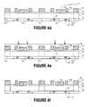
- FIGS. 4 a through 4 fare cross-sectional side views illustrating process steps of a method for fabricating the MEMS mirror device according to a first embodiment
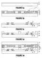
- FIGS. 5 a through 5 fare cross-sectional side views illustrating process steps of a method for fabricating the MEMS mirror device according to a second embodiment
- FIGS. 6 a through 6 fare cross-sectional side views illustrating process steps of a method for fabricating the MEMS mirror device according to a third embodiment
- FIG. 7 ais a top view of a MEMS mirror device according to another embodiment without electrodes and a wiring pattern
- FIG. 7 bis an illustration showing the cross-sectional side views along the lines B-B′, C-C′, D-D′, and E-E′ such as that shown in FIG. 7 a to show the thickness and width for the hinge pattern, frame pattern, mirror, and support structure;
- FIGS. 8 a through 8 fare cross-sectional side views illustrating process steps of a method for fabricating the MEMS mirror device according to a fourth embodiment.
- a micro-electro-mechanical-system (MEMS) mirror devicethat includes a substrate. Electrodes are formed supported by the substrate. A support structure is formed adjacent to the electrodes. A hinge pattern is formed on the support structure. A hinge pattern and a mirror pattern having a center mirror component are formed such that support structure supports the hinge pattern and mirror pattern. The support structure also supports the hinge pattern and mirror pattern such that a bottom surface of the center mirror component in a stationary non-rotating position is capable of exceeding a height of 50 ⁇ m above the electrodes. For example, the support structure may support the hinge pattern and mirror pattern such that the bottom surface of the center mirror component in a stationary non-rotating position has a height of about 100 ⁇ m above the electrodes.
- MEMSmicro-electro-mechanical-system
- the center mirror componentmay have a larger angular range of motion that can pivot about an axis.
- the center mirror componentis capable of having an angular range of motion exceeding 20 degrees with respect to an axis. Because the center mirror component may have such a large range of angular motion, the center mirror component may redirect light beams at a larger number of positions.
- such a MEMS mirror device having a large angular motioncan provide increased flexibility for optical switching systems, scanning systems, printing systems, and display systems that require redirecting beams of light.
- the methods for fabricating a MEMS mirror device as described hereinallow for a large number of mirror devices to be arranged on a single substrate.
- the methods for fabricating a MEMS mirror devicealso allow the center mirror component to be at a desired height above the electrodes or substrate dictated simply by a thickness of a substrate or a thickness of a formed support structure.
- a MEMS mirror device fabrication methodexposes selectively a substrate to form exposed regions and unexposed regions. Electrodes are formed supported by the substrate. A mirror pattern having a center mirror component and a hinge pattern are formed supported by the substrate. Portions of the substrate are removed in the exposed regions to form a support structure from the unexposed regions such that the support structure supports the mirror pattern and hinge pattern.
- a single substrateis used to fabricate a MEMS mirror device.
- the single substrateis used to form the electrodes, mirror pattern, hinge pattern, and support structure.
- the height at which a center mirror component is above the electrodesis dictated by the thickness of the substrate.
- a MEMS mirror device fabrication methodforms a release layer on a first substrate.
- a mirror pattern having a center mirror component and a hinge patternare formed supported by the release layer.
- Electrodesare formed supported by a second substrate.
- a support structureis formed. The first substrate and the second substrate are attached using the support structure. The first substrate and the release layer are removed such that the support structure supports the mirror pattern and hinge pattern.
- two substratesare used to fabricate a MEMS mirror device.
- the height at which the center mirror component is above the electrodesis dictated by a thickness of the formed support structure.
- a thickness of the formed support structureis formed.
- the thickness of the support structure formeddictates the height at which a center component is above the electrodes.
- a MEMS mirror device fabrication methodforms a release layer on a first substrate.
- a mirror pattern having a center mirror component and a hinge patternare formed supported by the release layer.
- Electrodesare formed supported by a second substrate.
- a support structureis formed using a third substrate. The first substrate is attached with the second substrate using the support structure. The first substrate and release layer are removed.
- three substratesare used to fabricate a MEMS mirror device.
- a first substrateis used to form the hinge pattern and mirror pattern.
- a second substrateis used to form the electrodes.
- a third substrateis used to form the support structure.
- the thickness of the third substrate useddictates the thickness of the support structure.
- the height at which the center mirror component is above the electrodesis simply dictated by the thickness of the gird substrate.
- a thicker third substrateis simply used.
- a MEMS mirror device fabrication methodforms electrodes supported by a first substrate. Portions of a second substrate are removed selectively on a bottom side. Portions of the second substrate are removed selectively on a topside to form a mirror pattern, frame pattern, hinge pattern, and support structure. The first substrate is attached with the second substrate.
- two substratesare used to fabricate a MEMS mirror device.
- the height at which the center mirror component is above the electrodesis dictated by the thickness of the second substrate used.
- the mirror pattern, frame pattern, hinge pattern, and support structurecan be formed from a single substrate.
- a layercan be selectively patterned on a substrate using any combination of a photolithography and dry or wet etching process or a liftoff process.
- a liftoff processinvolves depositing a photosensitive film over a substrate that is then exposed and developed to pattern the photosensitive film. Material is then deposited over the entire surface the substrate and on the patterned photosensitive film. After the material is deposited over the substrate and on the patterned photosensitive film, the patterned photosensitive film is dissolved and any material formed thereon is removed. As a result of this process, the material deposited is selectively patterned.
- a layermay also be removed or released by using oxygen plasma that reacts with the layer to release or remove the layer from an attached material.
- FIG. 1is top view of one embodiment of a MEMS mirror device without electrodes and a wiring pattern illustrating a first mirror device 9 A and a second mirror device 9 B having a support structure 5 , hinge pattern 6 , and mirror pattern 7 .
- Mirror pattern 7may include a center mirror component 7 a , frame pattern 7 b , and mirror component 7 c .
- Center mirror component 7 ais capable of having an angular range of motion with respect to an axis.
- Frame pattern 7 bprovides support for center mirror component 7 a .
- Mirror component 7 cmay be used for alignment or bonding purposes. Alternatively, mirror component 7 c may be omitted from mirror pattern 7 .
- FIG. 2is a complete top view of one embodiment of a MEMS mirror device such as that shown in FIG. 1 further illustrating electrodes 4 and wiring pattern 2 for the first mirror device 9 A and second mirror device 9 B.
- FIG. 3is a cross sectional side view showing the structure of one embodiment of a MEMS mirror device taken along the line A-A′ such as that shown in FIG. 2 .
- a MEMS mirror deviceincludes a substrate 1 having wiring pattern 2 formed thereon. Electrodes 4 are formed such that electrodes are coupled with wiring pattern 2 . An insulation layer 3 is formed to provide insulation for wiring pattern 2 and electrodes 4 .
- Support structure 5is formed on insulation layer 3 adjacent from electrodes 4 .
- Support structure 5may include a post structure to provide support for layers formed thereon or attached therewith.
- Support structure 5may define a honeycombed shape.
- Support structure 5may also define holes such that the holes are centered approximately below the center mirror component.
- Support structure 5provides support for hinge pattern 6 and mirror pattern 7 .
- Mirror pattern 7includes a center mirror component 7 a , frame pattern 7 b , and mirror component 7 c .
- mirror patternmay include center mirror component 7 a and frame pattern 7 b .
- Hinge pattern 6is attached with mirror pattern 7 and support structure 5 .
- Hinge pattern 6may be a thin and flexible material.
- Hinge pattern 6provides support for mirror pattern 7 .
- Frame pattern 7 bprovides support for center mirror component 7 a .
- Mirror component 7 cis supported by hinge pattern 6 and may be used for alignment or bonding purposes. Alternatively, mirror component 7 c may be omitted from mirror pattern 7 .
- the center mirror component 7 ais formed such that it is disposed above electrodes 4 .
- Center mirror component 7 aincludes a reflective surface to reflect beams of light.
- Electrodes 4are located below at opposing edges of center mirror component 7 a .
- Center mirror component 7 amay also be connected with a ground line (not shown) in substrate 1 for electrical shielding purposes.
- Electrodes 4are coupled with a respective wiring pattern 2 located on substrate 1 .
- a ground linemay be disposed between electrodes 4 and wiring pattern 2 for purposes of electrical shielding.
- Center mirror component 7 amay move about an axis to have an angular range of motion caused by electrostatic actuation from electrodes 4 .
- Electrostatic actuationis caused by a voltage being applied to electrodes 4 through wiring pattern 2 .
- a voltage applied to electrodes 4creates an electric field between, for example, electrodes 4 and center mirror component 7 a .
- the electric fieldis created near the edges of center mirror component 7 a .
- the electric fieldcauses center mirror component 7 a to have an angular range of motion with respect to an axis such as, for example, an axis parallel to hinge pattern 7 .
- the edges of center mirror component 7 a towards electrodes 4 at which the voltage is appliedmoves towards such electrodes 4 .
- center mirror component 7 aBy increasing the angular range of motion for center mirror component 7 a , center mirror component 7 a can redirect beams of light to a larger number of positions thereby increasing flexibility for optical switching.
- Increasing the thickness for support structure 5can increase the angular range of motion for center mirror component 7 a .
- Support structure 5 having an increased thicknessprovides a larger height for center mirror component 7 a to be off of substrate 1 . Because center mirror component 7 a may have a large height off substrate 1 , center mirror component 7 a is provided with a larger angular range of motion.
- the support structurecan be fabricated to support the hinge pattern and mirror pattern such that a bottom surface of the center mirror component in a stationary non-rotating position is capable of exceeding a height of 50 ⁇ m above the electrodes.
- the support structuremay support the hinge pattern and mirror pattern such that the bottom surface of the center mirror component in a stationary non-rotating position is capable of having a height about 100 ⁇ m above the electrodes.
- the following embodimentsprovide a center mirror component that is capable of having an angular range of motion exceeding 20 degrees with respect to an axis.
- FIGS. 4 a through 4 fare cross-sectional side views illustrating process steps of a method for fabricating the MEMS mirror device according to a first embodiment.
- substrate 10is exposed selectively on a first side to form exposed regions 11 a and unexposed regions 11 b in substrate 10 .
- a honeycombed maskmay be used to expose selectively substrate 10 .
- other masksmay be used to form exposed regions on a substrate such that mirror components are centered approximately over the exposed regions.
- the first sideis a topside of substrate 10 .
- Substrate 10is a substrate that can be etched more rapidly in the exposed regions than in the unexposed regions.
- substrate 10may be a photosensitive glass substrate that can be exposed selectively and etched more rapidly in the exposed regions than in the unexposed regions. After being exposed selectively, substrate 10 may be polished to retain planarity and remove any materials that may have formed on substrate 10 during this process.
- a first metal layeris formed on a second side of substrate 10 and is selectively patterned and etched to form electrodes 14 .
- the second sideis a bottom side of substrate 10 .
- the first metal layermay be a metallic layer such as, for example, an aluminum Al layer.
- an oxide layeris then formed over electrodes 14 and substrate 10 on the bottom side and selectively patterned to form insulation layer 13 , such that insulation layer 13 exposes portions of electrodes 14 .
- dielectric layersmay be used such as, for example, silicon dioxide SiO 2 layer, silicon nitride Si x N y layer, or silicon oxynitride Si x O y N z layer, that can be selectively patterned and etched to form insulation layer 13 .
- a second metal layeris formed on insulation layer 13 and on exposed portions of electrodes 14 and is selectively patterned and etched to form wiring pattern 12 .
- the second metal layermay also be a metallic layer such as, for example, an Al layer.
- Wiring pattern 12is formed such that it is coupled with electrodes 14 .
- Insulation layer 13provides insulation for wiring pattern 12 and electrodes 14 .
- a polysilicon layeris formed on the topside of substrate 10 .
- the polysilicon layeris selectively patterned and etched to form hinge pattern 16 .
- a polymer layer, oxide layer, nitride layer, silicon nitride Si x N y layer, silicon dioxide SiO 2 , layer, or silicon oxynitride Si x O y N z layermay be used that is selectively patterned and etched to form hinge pattern 16 .
- Hinge pattern 16is formed to be thin and flexible. Hinge pattern 16 is also formed such that portions of substrate 11 are exposed above an area near electrodes 14 .
- At least one layer having light reflective propertiesis formed on hinge pattern 16 and on the exposed portions of the topside of substrate 11 .
- a metal layer having light reflective propertiesmay be formed on hinge pattern 16 and portions of the exposed substrate 11 and selectively pattern and etched to form mirror pattern 17 .
- the metal layermay be a gold Au metal layer, aluminum Al metal layer, or a copper Cu metal layer.
- Mirror pattern 17includes a center mirror component 17 a , frame pattern 17 b , and mirror component 17 c .
- Frame pattern 17 bis supported by hinge pattern 16 .
- Frame pattern 17 bprovides support for center mirror component 17 a .
- Mirror component 17 cis supported by hinge pattern 16 .
- mirror component 17 cmay be omitted from mirror pattern 17 .
- mirror pattern 17Multiple layers may also be used to form mirror pattern 17 .
- a first metal layeris formed on hinge pattern 17 and on portions of the exposed substrate 11 .
- a support layeris formed on the first metal layer.
- a second metal layeris formed on the support layer. The three layers are selectively patterned and etched to form mirror pattern 17 .
- the first and second metal layersare layers having light reflective properties.
- a gold Au metal layer, an aluminum Al metal layer, or a copper Cu metal layermay be used for the first and second metal layers.
- the support layeris a layer that provides a flat surface and structural support.
- a silicon dioxide SiO 2 layer, silicon nitride Si x N y layer, polysilicon layer, silicon oxynitride Si x O y N z layer, or a polymer layermay be used for the support layer.
- the support layermay include the same material as the first and second metal layers.
- a polymer layeris formed over mirror pattern 17 and hinge pattern 16 and is patterned selectively and etched to form protection layer 18 .
- a polysilicon layer, oxide layer, or nitride layermay be used to form protection layer 18 .
- Protection layer 18is patterned to protect mirror pattern 17 and hinge pattern 16 .
- Protection layer 18is also patterned such that an etching solution can reach substrate 11 .
- a hydrofluoric (HF) acid etching solutionis used to etch substrate 11 .
- forming protection layer 18may be optional if mirror pattern 17 and hinge pattern 16 are resistant to the etching solution. If, for example, HF acid is used and hinge pattern 16 is made from an oxide material, which etches easily in HF acid, protection layer 18 (not made of an oxide) is then required.
- the etching solutionis deposited over substrate 11 to etch substrate 11 .
- HF acidis used that etches away the exposed regions 11 a more rapidly than the unexposed regions 11 b such that remaining portions of the unexposed regions 11 b of substrate 11 form support structure 15 .
- a protection layeris used, then the protection layer is removed using an oxygen plasma, wet, or dry etch process.
- the thusly-fabricated MEMS mirror deviceserves to provide a support structure using a single substrate.
- the single substrateis a photosensitive substrate.
- the photosensitive substrateis a photosensitive glass substrate that is exposed selectively. Because the photosensitive substrate is exposed selectively, the photosensitive substrate can be etched to form the support structure after forming the hinge pattern and mirror pattern. Thus, mounting a mirror pattern and a hinge pattern on a support structure is avoided. Furthermore, the thickness of the photosensitive substrate dictates the height at which a center mirror component is above the electrodes.
- FIGS. 5 a through 5 fare cross-sectional side views illustrating process steps of a method for fabricating the MEMS mirror device according to a second embodiment.
- a polymer layeris formed on a first substrate 20 to form a release layer 21 .
- Release layer 21may also be a layer that can be etched easily away or is removed easily from first substrate 20 .
- release layer 21may be a polysilicon layer, oxide layer, or a nitride layer.
- First substrate 20may be a silicon substrate, glass substrate, or a borosilicate glass substrate.
- At least one layer having light reflective propertiesis formed on release layer 21 .
- a metal layer having light reflective propertiesmay be formed on release layer and selectively pattern and etched to form mirror pattern 27 .
- the metal layermay be a gold Au metal layer, aluminum Al metal layer, or a copper Cu metal layer.
- Mirror pattern 27includes a center mirror component 27 a , frame pattern 27 b , and mirror component 27 c formed on release layer 21 .
- mirror component 27 cmay be omitted from mirror pattern 27 .
- mirror pattern 27Multiple layers may also be used to form mirror pattern 27 .
- a first metal layeris formed on release layer 21 .
- a support layeris formed on the first metal layer.
- a second metal layeris formed on the support layer. The three layers are selectively patterned and etched to form mirror pattern 27 .
- the first and second metal layersare layers having light reflective properties.
- a gold Au metal layer, an aluminum Al metal layer, or a copper Cu metal layermay be used for the first and second metal layers.
- the support layeris a layer that provides a flat surface and structural support.
- a silicon dioxide SiO 2 layer, silicon nitride Si x N y layer, polysilicon layer, silicon oxynitride Si x O y N z layer, or a polymer layermay be used for the support layer.
- the support layermay include the same material as the first and second metal layers.
- a polysilicon layeris formed over mirror pattern 27 and is selectively patterned and etched to form hinge pattern 26 .
- a polymer layer, oxide layer, nitride layer, silicon nitride Si x N y layer, silicon dioxide SiO 2, layer, or silicon oxynitride Si x O y N z layermay be used that is selectively patterned and etched to form hinge pattern 26 .
- Hinge pattern 26is formed on portions of mirror pattern 27 .
- Hinge pattern 26is not formed on center mirror component 27 a .
- Hinge pattern 26is formed to be thin and flexible.
- a first metal layeris formed on a second substrate 30 and is selectively patterned and etched to form wiring pattern 32 .
- Second substrate 30may be may be a silicon substrate, glass substrate, or borosilicate glass substrate.
- the first metal layermay be a metallic layer such as, for example, an aluminum Al layer.
- an oxide layeris then formed over wiring pattern 32 and second substrate 30 and is selectively patterned and etched to form insulation layer 33 . Insulation layer 33 is formed such that portions of wiring pattern 32 are exposed.
- dielectric layersmay be used such as, for example, silicon dioxide SiO 2 layer, silicon nitride Si x N y layer, or silicon oxynitride Si x O y N z layer, that can be selectively patterned and etched to form insulation layer 33 .
- a second metal layeris formed over insulation layer 33 and wiring pattern 32 and is selectively patterned and etched to form electrodes 34 .
- the second metal layermay also be a metallic layer such as, for example, an Al layer.
- Electrodes 34are formed such that they are coupled with wiring pattern 32 .
- Insulation 33provides insulation for wiring pattern 32 and electrodes 34 .
- a thick patterned filmis used to form support structure 35 .
- a metal plating processis used with the thick patterned film to form support structure 35 .
- an electroless metal deposition processmay be used to form support structure 35 .
- a thick photo resist filmis formed on insulation layer 33 and selectively patterned to allow support structure 35 to be formed therein on insulation layer 33 .
- a thick photo resist filmmay be formed on hinge pattern 26 and selectively patterned to allow support structure 35 to be formed on hinge pattern 26 .
- an aqueous solution having nickel Niis deposited over the patterned photo resist film such that nickel Ni is formed in the patterned thick photo resist film. After Ni is formed, the remaining photo resist film is removed to form support structure 35 made of Ni. Alternatively, an aqueous solution having copper Cu or gold Au may be used to form support structure 35 using the electroless metal deposition process. The remaining photo resist film is then removed.
- an electroplating process or a metal sputtering processmay be used.
- a thick photo resist filmis formed on insulation layer 33 and selectively patterned to allow support structure 35 to be formed therein on insulation layer 33 .
- a thick photo resist filmis formed on hinge pattern 26 and selectively patterned to allow support structure 35 to be formed therein on hinge pattern 26 .
- an electroplating solution having nickel Niis deposited over the patterned photo resist film and an electric current is passed through the solution such that Ni is formed in the patterned thick photo resist film.
- the remaining photo resist filmis removed to form support structure 35 made of Ni.
- an electro-plating solution having copper Cu or gold Aumay be used to form support structure 35 using the electroplating process.
- a thin conductive layer(not shown) may be formed selectively on insulation layer 33 or hinge pattern 26 to assist in the electroplating process. The photo resist film is then removed.
- a thick photo resist filmis formed on insulation layer 33 and selectively patterned to allow support structure 35 to be formed therein on insulation layer 33 .
- a thick photo resist filmis formed on hinge pattern 26 and selectively patterned to allow support structure 35 to be formed therein on hinge pattern 26 .
- metalis sputtered on the patterned thick photo resist film such that the metal is formed therein.
- metalis sputtered on the patterned thick photo resist film such that the metal is formed therein.
- nickel Ni, copper Cu, or gold Aumay be sputtered on the patterned thick photo resist film such that metal is formed therein.
- the remaining patterned thick photo resist film and metal formed thereonare removed to form support structure 35 .
- the thick photo resist filmis then removed.
- first substrate 20is attached with second substrate 30 . If support structure 35 is formed on insulation layer 33 , first substrate 20 may be attached with second substrate 30 by flipping first substrate 20 and bonding hinge pattern 26 with a top side of support structure 35 . Alternatively, if support structure 35 is formed on hinge pattern 26 , first substrate 20 may be attached with second substrate 30 by flipping first substrate 20 and bonding support structure 35 with insulation layer 33 .
- Support structure 35can be bonded to insulation layer 33 or hinge pattern 26 using a soldering bond technique that forms a bonding layer.
- a bonding layer 38may be formed to bond support structure 35 with hinge pattern 26 .
- a bonding layermay be formed near insulation layer 33 to bond support structure 35 with hinge pattern 26 .
- the bonding layermay include a lead-tin PbSn mixture.
- a thin metal layermay be formed on hinge pattern 26 or insulation layer 33 to assist in the bonding process.
- first substrate 20 and release layer 21are removed such that support structure 35 supports hinge pattern 26 .
- Hinge pattern 26supports mirror pattern 27 .
- First substrate 20may be removed using an etching or polishing process.
- first substrate 20may be etched away using hydro-fluoric (HF) acid or first substrate 20 may be polished away.
- Release layer 21may be removed using oxygen plasma, wet etch, or a dry etch process.
- the thusly fabricated MEMS mirror deviceserves to provide a support structure using a thick film process.
- the thickness of the thick photo resist film useddictates the thickness of support structure 35 .
- the thickness of support structure 35dictates the height in which a center mirror component is above the electrodes that determines angular range of motion for the center mirror component.
- FIGS. 6 a through 6 eare cross-sectional side views illustrating process steps of a method for fabricating the MEMS mirror device according to a third embodiment.
- the fabrication steps illustrated by FIG. 6 a to form release layer 41 , mirror pattern 47 , and hinge pattern 46are identical to the fabrication steps illustrated by FIGS. 5 a and 5 b for a first substrate 40 and accordingly descriptions to FIG. 6 a will be omitted.
- the fabrication steps illustrated by FIG. 6 b to form wiring pattern 52 , electrodes 54 , and insulation layer 53 using a second substrate 50are identical to the fabrication steps illustrated by FIG. 5 c and accordingly descriptions to FIG. 6 b will be omitted.
- a third substrate 60is used to form support structure 65 .
- Third substrate 60may be etched selectively to form support structure 65 .
- Third substratemay be a silicon substrate, glass substrate, or a borosilicate glass substrate.
- Third substrate 60may be etched selectively in areas 61 a of third substrate 60 using a reactive ion etching (RIE) process.
- RIEreactive ion etching
- the RIE etching processforms deep holes in third substrate 60 such that areas 61 b of third substrate 60 remain to form support structure 65 .
- deep holesmay be formed in third substrate 60 using a wet etch or a laser ablation process such that areas 61 a are removed from third substrate 60 .
- Third substrate 60may also be a photosensitive substrate that is exposed selectively to form exposed regions 61 a and unexposed regions 61 b in third substrate 60 .
- Third substrate 60is a substrate that can be etched more rapidly in the exposed regions than in the unexposed regions. After being exposed selectively, third substrate 60 may be polished to retain planarity and remove any materials that may have formed on third substrate 60 during this process.
- an etching solutionis used to etch third substrate 60 .
- HF acid etching solutionis deposited selectively over third substrate 60 to etch third substrate 60 .
- the HF addetches away the exposed regions 61 a more rapidly than the unexposed regions 61 b such that the remaining portions of the unexposed regions 61 b of third substrate 60 form support structure 65 .
- Support structure 65may define a honeycombed shape or define holes approximately centered with respect to center mirror components.
- first substrate 40is attached with second substrate 50 using support structure 65 .
- support structure 65is bonded with insulation layer 53 using a solder bond process thus forming a bonding layer 69 .
- hinge pattern 46is bonded with support structure 65 using a solder bond process thus forming a bonding layer 68 .
- support structure 65is bonded with hinge pattern 46 using a solder bond process thus forming a bonding layer 68 .
- insulation layeris bonded with support structure 65 thus forming bonding layer 69 .
- Bonding layers 68 and 69may include a lead-tin PbSn mixture.
- a thin metal layermay also be formed on insulation layer 53 and hinge pattern 46 to assist in the bonding process.
- first substrate 40is attached with second substrate 50 using support structure 65 .
- First substrate 40 and release layer 41are removed such that support structure 65 supports hinge pattern 46 .
- Hinge pattern 46supports mirror pattern 47 .
- First substrate 40may be removed using an etching or polishing process. For example, first substrate 40 may be etched away using HF add or first substrate 40 may be polished away. Release layer may be removed using an oxygen plasma, wet etch, or a dry etch process.
- the thusly fabricated MEMS mirror deviceuses three substrates.
- One substrateis used to form mirror pattern 47 and hinge pattern 46 .
- a second substrateis used to form electrodes 54
- a third substrate 50is used to form a support structure 65 .
- the height at which the center mirror component is above the electrodesis simply dictated by the thickness of the third substrate used. Thus, to increase the height of the center mirror component above the electrodes, a thicker substrate may be used.
- FIG. 7 ais a top view of a MEMS mirror device according to another embodiment without electrodes and a wiring pattern.
- FIG. 7 ashows a first mirror device 101 a and a second mirror device 101 b having a support structure 95 , hinge pattern 96 , frame pattern 97 , and mirror 97 a.
- Support structure 95 , hinge pattern 96 , frame pattern 97 , and mirror 97 aare all formed from a single substrate.
- Hinge pattern 96provides support for frame 97 b and mirror 97 a .
- Frame 97 bprovides support for mirror 97 a .
- Support structure 95provides support for hinge pattern 96 , frame pattern 97 b , and mirror 97 a .
- Mirror 97 ais capable of having an angular range of motion with respect to an axis.
- FIG. 7 bis an illustration showing the cross-sectional side views along the lines B-B′, C-C′, D-D′, and E-E′ such as that shown in FIG. 7 a to show the different thickness and width for the hinge pattern 96 , frame pattern 97 b , mirror 97 a , and support structure 95 , respectively, for first mirror 101 a and second mirror 101 b .
- hinge pattern 96is formed to have a smaller thickness than frame pattern 97 b and mirror 97 a .
- hinge pattern 96may be formed to have the same thickness as frame pattern 97 b and mirror 97 a .
- Frame pattern 97 b and mirror 97 aare formed to have the same thickness.
- FIGS. 8 a - 8 fare cross-sectional side views illustrating process steps of a method for fabricating the MEMS mirror device according to the fourth embodiment.
- FIG. 8 aillustrates the processing steps to form a wiring pattern, electrodes, insulation layer using a first substrate.
- the fabrication steps illustrated by FIG. 8 a to form wiring pattern 82 , electrodes 84 , insulation layer 83 using a first substrate 80are identical to the fabrication steps illustrated by FIGS. 5 c and 6 b and accordingly descriptions to FIG. 8 a will be omitted.
- FIGS. 8 b , 8 c , and 8 dillustrate the processing steps to form the hinge pattern, frame pattern, mirror, and support structure individually from a single substrate such as that shown in FIG. 7 b .
- the processing stepsare illustrated along the lines B-B′, C-C′, D-D′, E-E′ such as that shown in FIG. 7 a for mirror device 101 a and mirror device 101 b.
- a second substrate 90is etched selectively on a first side to remove large portions of second substrate 90 to define open areas (“windows”) 100 such that the open areas 100 are located below where hinge pattern 96 , mirror 97 a , and frame pattern 97 b will be formed.
- the first side of second substrate 90refers to a bottom side of second substrate 90 .
- a silicon etching processis used to etch selectively the bottom side of second substrate 90 .
- RIEreactive ion etching
- a wet etch or a laser ablation processmay be used to etch the bottom side of second substrate 90 to form open areas 100 .
- An oxide layeris deposited on a second side of second substrate 90 to form a mask layer 91 .
- a polymer layer, silicon nitride Si x N y layer, silicon oxynitride Si x O y N z layer, or a metal layermay be used to form mask layer 91 .
- Mask layer 91may also be formed prior to forming open areas 100 .
- the second siderefers to the topside of second substrate 90 .
- Mask layer 91is patterned to define hinge pattern 96 , frame pattern 97 b , mirror 97 a , and support structure 95 from second substrate 90 .
- FIGS. 8 c and 8 dillustrate the processing steps for forming hinge pattern 96 , frame pattern 97 b , mirror 97 a , and support structure 95 .
- the following process stepsdescribe forming hinge pattern 96 such that it has a smaller thickness than frame pattern 97 b and mirror 97 a .
- the following processing stepsmay be modified to form hinge pattern 96 having the same thickness as frame pattern 97 b and mirror 97 a.
- mask layer 91is patterned selectively on second substrate 90 to expose portions of second substrate 90 .
- the patterned mask layer 91defines hinge pattern 96 , frame pattern 97 b , mirror 97 a , and support structure 95 .
- the exposed portions of second substrate 90are etched using a silicon etching process.
- a RIE etching processmay be used to etch exposed portions of second substrate 90 to a first depth such that a thin portion (“floor”) of second substrate 90 remains above open areas 100 .
- a wet etch or a laser ablation processmay be used to etch the exposed portions of second substrate 90 to the first depth.
- an oxide layeris deposited over second substrate 90 and etched selectively to form sidewalls 94 .
- a polymer layer, silicon nitride Si x N y layer, silicon oxynitride Si x O y N z layer, or a metal layermay be used to form sidewalls 94 .
- Sidewalls 94provide protection to selective portions of the topside of second substrate 90 that define hinge pattern 96 , frame pattern 97 b , mirror 97 a , and support structure 95 , Layers that have formed on the floor in making sidewalls 94 are the etched to expose the floor.
- exposed portions of the floor of second substrate 90are etched using a silicon etching processes.
- a silicon etching processmay be used to etch exposed portions of the floor such that the floor falls below the sidewalls.
- a wet etch process or a laser ablation processmay be used to etch the exposed portions of the floor to fall below the sidewalls.
- a release processis performed to form hinge pattern 96 , frame pattern 97 b , and mirror 97 a .
- the release processis an etching process that undercuts selectively the exposed portions of the topside of second substrate 90 that defines hinge pattern 96 , frame pattern 97 b , and mirror 97 a underneath sidewalls 94 such that the floor is separated.
- hinge pattern 96is to have the same thickness as frame pattern 97 b and mirror 97 a , hinge pattern 96 , frame 97 b , and mirror 97 a are released at the same time. Alternatively, if hinge pattern 96 is to have a smaller thickness than frame pattern 97 b and mirror 97 a , frame pattern 97 b and mirror 97 a are released after hinge pattern 96 at a lower depth.
- the following stepdescribes the release process. To release frame pattern 97 b and mirror 97 a at a larger depth than hinge pattern 96 , the above steps are repeated such that exposed portions of the topside of second substrate 90 that define frame pattern 97 b and mirror 97 a underneath sidewalls 94 fall below hinge pattern 96 .
- a RIE etching processmay be used to release the exposed portions of the topside of second substrate that defines hinge pattern 96 , frame pattern 97 b , and mirror 97 a underneath sidewalls 94 to form hinge pattern 96 , frame pattern 97 b , and mirror 97 a from second substrate 90 .
- a time controlled profile etching processmay be used to release hinge pattern 96 , frame pattern 97 b , and mirror 97 a from second substrate 96 .
- the release processmay undercut frame pattern 97 b and mirror 97 a underneath sidewalls 94 such that non-straight edge surfaces are formed.
- the release processmay undercut hinge pattern 96 such that non-straight edge surfaces are also formed.
- Hinge pattern 96 , frame pattern 97 b , and mirror 97 aare thus formed after it has been released from second substrate 90 , and the remaining mask layer 91 and sidewalls 94 are removed.
- mask layer 91 and sidewalls 94may remain in forming the MEMS mirror device.
- the next step in the processis to remove the floor (“clear the floor”).
- the flooris etched away to clear the floor such that hinge pattern 96 , frame pattern 97 b , and mirror 97 a are suspended about support structure 95 and second substrate 90 .
- the floor of second substrate 90may be etched away using an RIE etching process.
- a wet etch or a laser ablation processmay be used to etch the exposed portions of the floor to clear the floor.
- Second substrate 90may also be flipped and the floor may be cleared from the back side using the same etching processes.
- support structure 95is thusly formed.
- support structure 95 , hinge pattern 96 , frame pattern 97 b , and mirror 97 aare illustrated with straight surfaces, but may have non-straight edge surfaces.
- FIG. 8 eis a cross-sectional side of the thusly formed hinge pattern 96 , frame pattern 97 b , mirror 97 a , and support structure 95 taken along the line A-A′ such as that shown in FIG. 7 a with showing electrodes.
- support structure 95provides support for hinge pattern 96 , frame pattern 97 b , and mirror 97 a .
- Hinge pattern 96 bprovides support for frame pattern 97 b .
- Frame pattern 97 bprovides support for mirror 97 a.
- a reflective material 97 a ′may then be formed on a top surface of mirror 97 a .
- Reflective material 97 a ′provides a reflective surface for mirror 97 a , which is used to redirect beams of light.
- reflective material 97 a ′may be formed on frame pattern 97 b and hinge pattern 96 .
- Reflective material 97 a ′includes at least one layer.
- reflective material 97 a ′may include a metal layer such as, for example, a gold Au metal layer, an aluminum metal layer, or a copper Cu metal layer.
- reflective material 97 a ′may be formed after the processing steps as illustrated in FIG. 8 e or after first substrate 80 is attached with second substrate 90 .
- FIG. 8 fillustrate attaching first substrate 80 with second substrate 90 to form the MEMS mirror device according to the fourth embodiment.
- first substrate 80is attached with second substrate 90 using support structure 95 .
- support structure 95is bonded with insulation layer 83 using a solder bond process thus forming a bonding layer 98 .
- Bonding layer 98may include a lead-tin PbSn mixture.
- a thin metal layermay also be formed on insulation layer 83 and a bottom side of support structure 95 to assist in the bonding process.
- the MEMS mirror deviceincludes first substrate 80 , wiring pattern 82 , insulation layer 83 , and electrodes 84 .
- First substrate 80 , wiring pattern 82 , insulation layer 83 , and electrodes 84are constructed and operate in a similar manner as substrate 1 , wiring pattern 2 , insulation layer 3 , and electrodes 4 , respectively, of FIG. 3 .
- the MEMS mirror devicealso includes a support structure 95 , hinge pattern 96 , frame pattern 97 b , and mirror 97 a .
- Support structure 95 , hinge pattern 96 , frame pattern 97 b , and mirror 97 aare made from a second substrate, which is separate from first substrate 80 .
- the substrate to form support structure 95 , hinge pattern 96 , frame pattern 97 b , and mirror 97 amay be a single crystal silicon (SCS) substrate or a substrate in which deep holes may be formed.
- Support structure 95 , hinge pattern 96 , frame pattern 97 b , and mirror 97 aare formed as a single unit.
- Support structure 95 , mirror 97 a , frame pattern 97 b , and hinge pattern 96operate in a similar manner as support structure 5 , center mirror component 7 a , frame pattern 7 b , and hinge pattern 6 , respectively, of FIG. 3 .
- the thusly fabricated MEMS mirror deviceuses two substrates.
- One substrateis used to form electrodes 84 , wiring pattern 82 , and insulation layer 83 .
- a second substrateis used to form support structure 95 , mirror 97 a , hinge pattern 96 , and frame pattern 97 b .
- the height at which the mirror is above the electrodesis simply dictated by the thickness of the second substrate used.
- a thicker second substratemay be used.
- the mirror, frame pattern, and hinge patternare formed without using thin film layering, which reduces the number of processing steps.
Landscapes
- Physics & Mathematics (AREA)
- General Physics & Mathematics (AREA)
- Optics & Photonics (AREA)
- Engineering & Computer Science (AREA)
- Computer Hardware Design (AREA)
- Microelectronics & Electronic Packaging (AREA)
- Mechanical Light Control Or Optical Switches (AREA)
- Micromachines (AREA)
Abstract
Description
Claims (68)
Priority Applications (1)
| Application Number | Priority Date | Filing Date | Title |
|---|---|---|---|
| US09/929,900US6563106B1 (en) | 2000-02-01 | 2001-08-14 | Micro-electro-mechanical-system (MEMS) mirror device and methods for fabricating the same |
Applications Claiming Priority (2)
| Application Number | Priority Date | Filing Date | Title |
|---|---|---|---|
| US09/497,270US20020071169A1 (en) | 2000-02-01 | 2000-02-01 | Micro-electro-mechanical-system (MEMS) mirror device |
| US09/929,900US6563106B1 (en) | 2000-02-01 | 2001-08-14 | Micro-electro-mechanical-system (MEMS) mirror device and methods for fabricating the same |
Related Parent Applications (1)
| Application Number | Title | Priority Date | Filing Date |
|---|---|---|---|
| US09/497,270DivisionUS20020071169A1 (en) | 2000-02-01 | 2000-02-01 | Micro-electro-mechanical-system (MEMS) mirror device |
Publications (1)
| Publication Number | Publication Date |
|---|---|
| US6563106B1true US6563106B1 (en) | 2003-05-13 |
Family
ID=23976147
Family Applications (2)
| Application Number | Title | Priority Date | Filing Date |
|---|---|---|---|
| US09/497,270AbandonedUS20020071169A1 (en) | 2000-02-01 | 2000-02-01 | Micro-electro-mechanical-system (MEMS) mirror device |
| US09/929,900Expired - LifetimeUS6563106B1 (en) | 2000-02-01 | 2001-08-14 | Micro-electro-mechanical-system (MEMS) mirror device and methods for fabricating the same |
Family Applications Before (1)
| Application Number | Title | Priority Date | Filing Date |
|---|---|---|---|
| US09/497,270AbandonedUS20020071169A1 (en) | 2000-02-01 | 2000-02-01 | Micro-electro-mechanical-system (MEMS) mirror device |
Country Status (3)
| Country | Link |
|---|---|
| US (2) | US20020071169A1 (en) |
| AU (1) | AU2001233228A1 (en) |
| WO (1) | WO2001056919A2 (en) |
Cited By (49)
| Publication number | Priority date | Publication date | Assignee | Title |
|---|---|---|---|---|
| US20030122206A1 (en)* | 2001-11-09 | 2003-07-03 | Amal Bhattarai | Multi-chip module integrating MEMS mirror array with electronics |
| US20030161027A1 (en)* | 2001-06-26 | 2003-08-28 | Seiko Epson Corporation | Light modulator and method of manufacturing the same |
| US20030205804A1 (en)* | 2001-12-31 | 2003-11-06 | Jin-Yuan Lee | Integrated chip package structure using ceramic substrate and method of manufacturing the same |
| US20040036949A1 (en)* | 2002-03-19 | 2004-02-26 | John Trezza | Combination micromachine and optical device array |
| US6734512B2 (en)* | 2001-10-24 | 2004-05-11 | Nec Corporation | Electrostatic actuator |
| US20040246306A1 (en)* | 2000-02-03 | 2004-12-09 | Scott Adams | Electrostatic actuator for microelectromechanical systems and methods of fabrication |
| US20050136663A1 (en)* | 2003-12-19 | 2005-06-23 | Agency For Science, Technology And Research | Single-crystal-silicon 3D micromirror |
| FR2864634A1 (en)* | 2003-12-26 | 2005-07-01 | Commissariat Energie Atomique | Production of a mechanical driving system for an optical component, notably for adaptive optical components and micro-mirrors |
| US20050280331A1 (en)* | 2004-06-18 | 2005-12-22 | Walsin Lihwa Corp. | Two-axis device and manufacturing method therefor |
| US20060087716A1 (en)* | 2004-10-27 | 2006-04-27 | Samsung Electronics Co., Ltd. | Micro thin-film structure, MEMS switch employing such a micro thin-film, and method of fabricating them |
| US7065736B1 (en) | 2003-09-24 | 2006-06-20 | Sandia Corporation | System for generating two-dimensional masks from a three-dimensional model using topological analysis |
| US20060132898A1 (en)* | 2004-12-22 | 2006-06-22 | Texas Instruments Incorporated | Structure and method for reducing thermal stresses on a torsional hinged device |
| US20060195019A1 (en)* | 2004-10-05 | 2006-08-31 | Agency For Science, Technology And Research | Microprobe for 3D bio-imaging, method for fabricating the same and use thereof |
| US20060228896A1 (en)* | 2005-03-31 | 2006-10-12 | Greywall Dennis S | Fabricating integrated devices using embedded masks |
| KR100650876B1 (en)* | 2005-12-26 | 2006-11-28 | 동부일렉트로닉스 주식회사 | Digital Micromirror Device and Manufacturing Method Thereof |
| US20070001247A1 (en)* | 2000-12-07 | 2007-01-04 | Patel Satyadev R | Methods for depositing, releasing and packaging micro-electromechanical devices on wafer substrates |
| US7173426B1 (en) | 2005-11-29 | 2007-02-06 | General Electric Company | Optical link for transmitting data through air from a plurality of receiver coils in a magnetic resonance imaging system |
| US7190854B1 (en)* | 2000-05-24 | 2007-03-13 | Active Optical Networks, Inc. | Methods for forming an array of MEMS optical elements |
| DE102006003718A1 (en)* | 2006-01-26 | 2007-08-09 | Atmel Germany Gmbh | Manufacturing process for integrated micro-electro-mechanical components |
| US7561317B2 (en) | 2006-11-03 | 2009-07-14 | Ethicon Endo-Surgery, Inc. | Resonant Fourier scanning |
| US7589316B2 (en) | 2007-01-18 | 2009-09-15 | Ethicon Endo-Surgery, Inc. | Scanning beam imaging with adjustable detector sensitivity or gain |
| US7713265B2 (en) | 2006-12-22 | 2010-05-11 | Ethicon Endo-Surgery, Inc. | Apparatus and method for medically treating a tattoo |
| US7728339B1 (en) | 2002-05-03 | 2010-06-01 | Calient Networks, Inc. | Boundary isolation for microelectromechanical devices |
| US20100307150A1 (en)* | 2007-12-14 | 2010-12-09 | University Of Florida Research Foundation, Inc. | Electrothermal microactuator for large vertical displacement without tilt or lateral shift |
| US7925333B2 (en) | 2007-08-28 | 2011-04-12 | Ethicon Endo-Surgery, Inc. | Medical device including scanned beam unit with operational control features |
| US7982776B2 (en) | 2007-07-13 | 2011-07-19 | Ethicon Endo-Surgery, Inc. | SBI motion artifact removal apparatus and method |
| US7983739B2 (en) | 2007-08-27 | 2011-07-19 | Ethicon Endo-Surgery, Inc. | Position tracking and control for a scanning assembly |
| US7995045B2 (en) | 2007-04-13 | 2011-08-09 | Ethicon Endo-Surgery, Inc. | Combined SBI and conventional image processor |
| US8050520B2 (en) | 2008-03-27 | 2011-11-01 | Ethicon Endo-Surgery, Inc. | Method for creating a pixel image from sampled data of a scanned beam imager |
| US8160678B2 (en) | 2007-06-18 | 2012-04-17 | Ethicon Endo-Surgery, Inc. | Methods and devices for repairing damaged or diseased tissue using a scanning beam assembly |
| US8216214B2 (en) | 2007-03-12 | 2012-07-10 | Ethicon Endo-Surgery, Inc. | Power modulation of a scanning beam for imaging, therapy, and/or diagnosis |
| US8273015B2 (en) | 2007-01-09 | 2012-09-25 | Ethicon Endo-Surgery, Inc. | Methods for imaging the anatomy with an anatomically secured scanner assembly |
| US8332014B2 (en) | 2008-04-25 | 2012-12-11 | Ethicon Endo-Surgery, Inc. | Scanned beam device and method using same which measures the reflectance of patient tissue |
| US8399988B2 (en) | 1999-03-01 | 2013-03-19 | Megica Corporation | High performance sub-system design and assembly |
| US8421222B2 (en) | 2002-10-25 | 2013-04-16 | Megica Corporation | Chip package having a chip combined with a substrate via a copper pillar |
| US8426958B2 (en) | 2005-05-03 | 2013-04-23 | Megica Corporation | Stacked chip package with redistribution lines |
| US8471361B2 (en) | 2001-12-31 | 2013-06-25 | Megica Corporation | Integrated chip package structure using organic substrate and method of manufacturing the same |
| US8492870B2 (en) | 2002-01-19 | 2013-07-23 | Megica Corporation | Semiconductor package with interconnect layers |
| US8626271B2 (en) | 2007-04-13 | 2014-01-07 | Ethicon Endo-Surgery, Inc. | System and method using fluorescence to examine within a patient's anatomy |
| US8801606B2 (en) | 2007-01-09 | 2014-08-12 | Ethicon Endo-Surgery, Inc. | Method of in vivo monitoring using an imaging system including scanned beam imaging unit |
| US9030029B2 (en) | 2001-12-31 | 2015-05-12 | Qualcomm Incorporated | Chip package with die and substrate |
| WO2015092938A1 (en)* | 2013-12-20 | 2015-06-25 | パイオニア株式会社 | Drive device |
| US9079762B2 (en) | 2006-09-22 | 2015-07-14 | Ethicon Endo-Surgery, Inc. | Micro-electromechanical device |
| US9125552B2 (en) | 2007-07-31 | 2015-09-08 | Ethicon Endo-Surgery, Inc. | Optical scanning module and means for attaching the module to medical instruments for introducing the module into the anatomy |
| US20180031822A1 (en)* | 2016-07-28 | 2018-02-01 | Stmicroelectronics S.R.L. | Process for manufacturing a mems micromirror device, and associated device |
| US20190071303A1 (en)* | 2017-09-04 | 2019-03-07 | Infineon Technologies Ag | Method for processing a layer structure and microelectromechanical component |
| US10399179B2 (en) | 2016-12-14 | 2019-09-03 | General Electric Company | Additive manufacturing systems and methods |
| US11085947B2 (en)* | 2018-08-21 | 2021-08-10 | Seiko Epson Corporation | Inertial sensor, sensor device, electronic device, and vehicle |
| US11994785B2 (en) | 2020-06-03 | 2024-05-28 | Raytheon Company | Dispersive beam steering based on optical-frequency shift patterns |
Families Citing this family (116)
| Publication number | Priority date | Publication date | Assignee | Title |
|---|---|---|---|---|
| US7550794B2 (en) | 2002-09-20 | 2009-06-23 | Idc, Llc | Micromechanical systems device comprising a displaceable electrode and a charge-trapping layer |
| US7297471B1 (en) | 2003-04-15 | 2007-11-20 | Idc, Llc | Method for manufacturing an array of interferometric modulators |
| US6632374B1 (en)* | 2000-09-28 | 2003-10-14 | Xerox Corporation | Method for an optical switch on a silicon on insulator substrate |
| US6632373B1 (en)* | 2000-09-28 | 2003-10-14 | Xerox Corporation | Method for an optical switch on a substrate |
| DE60116969T2 (en)* | 2000-09-28 | 2006-07-27 | Xerox Corp. | Production of a mirror structure |
| US6504643B1 (en)* | 2000-09-28 | 2003-01-07 | Xerox Corporation | Structure for an optical switch on a substrate |
| US6618184B2 (en)* | 2001-04-03 | 2003-09-09 | Agere Systems Inc. | Device for use with a micro-electro-mechanical system (MEMS) optical device and a method of manufacture therefor |
| US6704475B2 (en)* | 2001-04-03 | 2004-03-09 | Agere Systems Inc. | Mirror for use with a micro-electro-mechanical system (MEMS) optical device and a method of manufacture therefor |
| EP1518822A3 (en)* | 2001-12-06 | 2007-02-28 | Microfabrica Inc. | Complex microdevices and apparatus and methods for fabricating such devices |
| US6794119B2 (en) | 2002-02-12 | 2004-09-21 | Iridigm Display Corporation | Method for fabricating a structure for a microelectromechanical systems (MEMS) device |
| US6992810B2 (en)* | 2002-06-19 | 2006-01-31 | Miradia Inc. | High fill ratio reflective spatial light modulator with hidden hinge |
| US7206110B2 (en)* | 2002-06-19 | 2007-04-17 | Miradia Inc. | Memory cell dual protection |
| US20040069742A1 (en)* | 2002-06-19 | 2004-04-15 | Pan Shaoher X. | Fabrication of a reflective spatial light modulator |
| US20040004753A1 (en)* | 2002-06-19 | 2004-01-08 | Pan Shaoher X. | Architecture of a reflective spatial light modulator |
| US20030234994A1 (en)* | 2002-06-19 | 2003-12-25 | Pan Shaoher X. | Reflective spatial light modulator |
| US7034984B2 (en)* | 2002-06-19 | 2006-04-25 | Miradia Inc. | Fabrication of a high fill ratio reflective spatial light modulator with hidden hinge |
| US20040024582A1 (en)* | 2002-07-03 | 2004-02-05 | Scott Shepard | Systems and methods for aiding human translation |
| US7208809B2 (en)* | 2002-09-19 | 2007-04-24 | Nippon Telegraph And Telephone Corporation | Semiconductor device having MEMS |
| US7781850B2 (en) | 2002-09-20 | 2010-08-24 | Qualcomm Mems Technologies, Inc. | Controlling electromechanical behavior of structures within a microelectromechanical systems device |
| US7138293B2 (en)* | 2002-10-04 | 2006-11-21 | Dalsa Semiconductor Inc. | Wafer level packaging technique for microdevices |
| JP4550578B2 (en)* | 2002-10-10 | 2010-09-22 | 富士通株式会社 | Micro movable element with torsion bar |
| TW594360B (en) | 2003-04-21 | 2004-06-21 | Prime View Int Corp Ltd | A method for fabricating an interference display cell |
| US7095546B2 (en) | 2003-04-24 | 2006-08-22 | Metconnex Canada Inc. | Micro-electro-mechanical-system two dimensional mirror with articulated suspension structures for high fill factor arrays |
| TW570896B (en) | 2003-05-26 | 2004-01-11 | Prime View Int Co Ltd | A method for fabricating an interference display cell |
| US7221495B2 (en)* | 2003-06-24 | 2007-05-22 | Idc Llc | Thin film precursor stack for MEMS manufacturing |
| TWI231865B (en) | 2003-08-26 | 2005-05-01 | Prime View Int Co Ltd | An interference display cell and fabrication method thereof |
| TW593126B (en)* | 2003-09-30 | 2004-06-21 | Prime View Int Co Ltd | A structure of a micro electro mechanical system and manufacturing the same |
| US7012726B1 (en) | 2003-11-03 | 2006-03-14 | Idc, Llc | MEMS devices with unreleased thin film components |
| US7026695B2 (en)* | 2003-11-19 | 2006-04-11 | Miradia Inc. | Method and apparatus to reduce parasitic forces in electro-mechanical systems |
| US7295726B1 (en) | 2003-12-02 | 2007-11-13 | Adriatic Research Institute | Gimbal-less micro-electro-mechanical-system tip-tilt and tip-tilt-piston actuators and a method for forming the same |
| US7428353B1 (en) | 2003-12-02 | 2008-09-23 | Adriatic Research Institute | MEMS device control with filtered voltage signal shaping |
| US20050255666A1 (en)* | 2004-05-11 | 2005-11-17 | Miradia Inc. | Method and structure for aligning mechanical based device to integrated circuits |
| US7449284B2 (en) | 2004-05-11 | 2008-11-11 | Miradia Inc. | Method and structure for fabricating mechanical mirror structures using backside alignment techniques |
| US7042619B1 (en) | 2004-06-18 | 2006-05-09 | Miradia Inc. | Mirror structure with single crystal silicon cross-member |
| US7068417B2 (en)* | 2004-07-28 | 2006-06-27 | Miradia Inc. | Method and apparatus for a reflective spatial light modulator with a flexible pedestal |
| US7081728B2 (en)* | 2004-08-27 | 2006-07-25 | Sequence Controls Inc. | Apparatus for controlling heat generation and recovery in an induction motor |
| US7417783B2 (en) | 2004-09-27 | 2008-08-26 | Idc, Llc | Mirror and mirror layer for optical modulator and method |
| US7373026B2 (en) | 2004-09-27 | 2008-05-13 | Idc, Llc | MEMS device fabricated on a pre-patterned substrate |
| US7553684B2 (en) | 2004-09-27 | 2009-06-30 | Idc, Llc | Method of fabricating interferometric devices using lift-off processing techniques |
| US7161730B2 (en)* | 2004-09-27 | 2007-01-09 | Idc, Llc | System and method for providing thermal compensation for an interferometric modulator display |
| US7405861B2 (en) | 2004-09-27 | 2008-07-29 | Idc, Llc | Method and device for protecting interferometric modulators from electrostatic discharge |
| US7349136B2 (en) | 2004-09-27 | 2008-03-25 | Idc, Llc | Method and device for a display having transparent components integrated therein |
| US7369296B2 (en) | 2004-09-27 | 2008-05-06 | Idc, Llc | Device and method for modifying actuation voltage thresholds of a deformable membrane in an interferometric modulator |
| US7492502B2 (en) | 2004-09-27 | 2009-02-17 | Idc, Llc | Method of fabricating a free-standing microstructure |
| US7429334B2 (en) | 2004-09-27 | 2008-09-30 | Idc, Llc | Methods of fabricating interferometric modulators by selectively removing a material |
| US7684104B2 (en) | 2004-09-27 | 2010-03-23 | Idc, Llc | MEMS using filler material and method |
| KR100624436B1 (en)* | 2004-10-19 | 2006-09-15 | 삼성전자주식회사 | 2-axis actuator and its manufacturing method |
| IL165212A (en) | 2004-11-15 | 2012-05-31 | Elbit Systems Electro Optics Elop Ltd | Device for scanning light |
| US8207004B2 (en)* | 2005-01-03 | 2012-06-26 | Miradia Inc. | Method and structure for forming a gyroscope and accelerometer |
| US7172921B2 (en)* | 2005-01-03 | 2007-02-06 | Miradia Inc. | Method and structure for forming an integrated spatial light modulator |
| US7199918B2 (en)* | 2005-01-07 | 2007-04-03 | Miradia Inc. | Electrical contact method and structure for deflection devices formed in an array configuration |
| US7142349B2 (en)* | 2005-01-07 | 2006-11-28 | Miradia Inc. | Method and structure for reducing parasitic influences of deflection devices on spatial light modulators |
| TW200628877A (en) | 2005-02-04 | 2006-08-16 | Prime View Int Co Ltd | Method of manufacturing optical interference type color display |
| US7432629B2 (en)* | 2005-02-16 | 2008-10-07 | Jds Uniphase Corporation | Articulated MEMs structures |
| US7457033B2 (en)* | 2005-05-27 | 2008-11-25 | The Regents Of The University Of California | MEMS tunable vertical-cavity semiconductor optical amplifier |
| US7202989B2 (en) | 2005-06-01 | 2007-04-10 | Miradia Inc. | Method and device for fabricating a release structure to facilitate bonding of mirror devices onto a substrate |
| US7298539B2 (en)* | 2005-06-01 | 2007-11-20 | Miradia Inc. | Co-planar surface and torsion device mirror structure and method of manufacture for optical displays |
| US7190508B2 (en) | 2005-06-15 | 2007-03-13 | Miradia Inc. | Method and structure of patterning landing pad structures for spatial light modulators |
| US7184195B2 (en) | 2005-06-15 | 2007-02-27 | Miradia Inc. | Method and structure reducing parasitic influences of deflection devices in an integrated spatial light modulator |
| US7372617B2 (en)* | 2005-07-06 | 2008-05-13 | Peter Enoksson | Hidden hinge MEMS device |
| KR101375337B1 (en)* | 2005-07-22 | 2014-03-18 | 퀄컴 엠이엠에스 테크놀로지스, 인크. | Electomechanical devices having support structures and methods of fabricating the same |
| CN101228091A (en) | 2005-07-22 | 2008-07-23 | 高通股份有限公司 | Support structures and methods for MEMS devices |
| EP2495212A3 (en) | 2005-07-22 | 2012-10-31 | QUALCOMM MEMS Technologies, Inc. | Mems devices having support structures and methods of fabricating the same |
| KR20080041663A (en) | 2005-07-22 | 2008-05-13 | 콸콤 인코포레이티드 | Supporting structures for MEMS devices and methods thereof |
| US7502158B2 (en) | 2005-10-13 | 2009-03-10 | Miradia Inc. | Method and structure for high fill factor spatial light modulator with integrated spacer layer |
| US7630114B2 (en) | 2005-10-28 | 2009-12-08 | Idc, Llc | Diffusion barrier layer for MEMS devices |
| US7416908B2 (en)* | 2005-12-14 | 2008-08-26 | Spatial Photonics, Inc. | Method for fabricating a micro structure |
| US7795061B2 (en) | 2005-12-29 | 2010-09-14 | Qualcomm Mems Technologies, Inc. | Method of creating MEMS device cavities by a non-etching process |
| US7382515B2 (en) | 2006-01-18 | 2008-06-03 | Qualcomm Mems Technologies, Inc. | Silicon-rich silicon nitrides as etch stops in MEMS manufacture |
| US7547568B2 (en) | 2006-02-22 | 2009-06-16 | Qualcomm Mems Technologies, Inc. | Electrical conditioning of MEMS device and insulating layer thereof |
| US7450295B2 (en) | 2006-03-02 | 2008-11-11 | Qualcomm Mems Technologies, Inc. | Methods for producing MEMS with protective coatings using multi-component sacrificial layers |
| US7643203B2 (en) | 2006-04-10 | 2010-01-05 | Qualcomm Mems Technologies, Inc. | Interferometric optical display system with broadband characteristics |
| US7527996B2 (en) | 2006-04-19 | 2009-05-05 | Qualcomm Mems Technologies, Inc. | Non-planar surface structures and process for microelectromechanical systems |
| US7711239B2 (en) | 2006-04-19 | 2010-05-04 | Qualcomm Mems Technologies, Inc. | Microelectromechanical device and method utilizing nanoparticles |
| US7623287B2 (en) | 2006-04-19 | 2009-11-24 | Qualcomm Mems Technologies, Inc. | Non-planar surface structures and process for microelectromechanical systems |
| US7417784B2 (en) | 2006-04-19 | 2008-08-26 | Qualcomm Mems Technologies, Inc. | Microelectromechanical device and method utilizing a porous surface |
| US7369292B2 (en) | 2006-05-03 | 2008-05-06 | Qualcomm Mems Technologies, Inc. | Electrode and interconnect materials for MEMS devices |
| US7405863B2 (en) | 2006-06-01 | 2008-07-29 | Qualcomm Mems Technologies, Inc. | Patterning of mechanical layer in MEMS to reduce stresses at supports |
| US7321457B2 (en) | 2006-06-01 | 2008-01-22 | Qualcomm Incorporated | Process and structure for fabrication of MEMS device having isolated edge posts |
| KR100846569B1 (en)* | 2006-06-14 | 2008-07-15 | 매그나칩 반도체 유한회사 | Package of MEMS element and manufacturing method thereof |
| KR100766600B1 (en)* | 2006-07-18 | 2007-10-12 | 삼성전자주식회사 | scanner |
| JP4327183B2 (en)* | 2006-07-31 | 2009-09-09 | 株式会社日立製作所 | High pressure fuel pump control device for internal combustion engine |
| US7763546B2 (en) | 2006-08-02 | 2010-07-27 | Qualcomm Mems Technologies, Inc. | Methods for reducing surface charges during the manufacture of microelectromechanical systems devices |
| US7566664B2 (en) | 2006-08-02 | 2009-07-28 | Qualcomm Mems Technologies, Inc. | Selective etching of MEMS using gaseous halides and reactive co-etchants |
| JP2008051992A (en)* | 2006-08-24 | 2008-03-06 | Olympus Corp | Micro mirror array device |
| US7545552B2 (en) | 2006-10-19 | 2009-06-09 | Qualcomm Mems Technologies, Inc. | Sacrificial spacer process and resultant structure for MEMS support structure |
| US7719752B2 (en) | 2007-05-11 | 2010-05-18 | Qualcomm Mems Technologies, Inc. | MEMS structures, methods of fabricating MEMS components on separate substrates and assembly of same |
| US8068268B2 (en) | 2007-07-03 | 2011-11-29 | Qualcomm Mems Technologies, Inc. | MEMS devices having improved uniformity and methods for making them |
| KR101001666B1 (en)* | 2008-07-08 | 2010-12-15 | 광주과학기술원 | Manufacturing method of micro vertical structure |
| US7924441B1 (en) | 2008-08-08 | 2011-04-12 | Mirrorcle Technologies, Inc. | Fast and high-precision 3D tracking and position measurement with MEMS micromirrors |
| US7719754B2 (en)* | 2008-09-30 | 2010-05-18 | Qualcomm Mems Technologies, Inc. | Multi-thickness layers for MEMS and mask-saving sequence for same |
| DE102008054784B4 (en) | 2008-12-17 | 2021-09-16 | Robert Bosch Gmbh | Micromirrors |
| US10739460B2 (en) | 2010-08-11 | 2020-08-11 | Apple Inc. | Time-of-flight detector with single-axis scan |
| WO2012020380A1 (en) | 2010-08-11 | 2012-02-16 | Primesense Ltd. | Scanning projectors and image capture modules for 3d mapping |
| US8659816B2 (en) | 2011-04-25 | 2014-02-25 | Qualcomm Mems Technologies, Inc. | Mechanical layer and methods of making the same |
| CN102496611B (en)* | 2011-12-31 | 2016-03-16 | 上海集成电路研发中心有限公司 | For the reliability testing of integrated circuit metal interconnection or the structure of MEMS electrode layer |
| CN104160240B (en)* | 2012-02-15 | 2017-02-22 | 苹果公司 | Scanning depth engine |
| EP2828833B1 (en)* | 2012-03-22 | 2017-03-08 | Apple Inc. | Gimbaled scanning mirror array |
| WO2014016794A1 (en) | 2012-07-26 | 2014-01-30 | Primesense Ltd. | Dual-axis scanning mirror |
| WO2014064606A1 (en)* | 2012-10-23 | 2014-05-01 | Primesense Ltd. | Production of micro-mechanical devices |
| US9267787B2 (en) | 2013-03-15 | 2016-02-23 | Apple Inc. | Depth scanning with multiple emitters |
| US9784838B1 (en) | 2014-11-26 | 2017-10-10 | Apple Inc. | Compact scanner with gimbaled optics |
| US9835853B1 (en) | 2014-11-26 | 2017-12-05 | Apple Inc. | MEMS scanner with mirrors of different sizes |
| US9798135B2 (en) | 2015-02-16 | 2017-10-24 | Apple Inc. | Hybrid MEMS scanning module |
| US9525863B2 (en) | 2015-04-29 | 2016-12-20 | Apple Inc. | Time-of-flight depth mapping with flexible scan pattern |
| US9897801B2 (en) | 2015-09-30 | 2018-02-20 | Apple Inc. | Multi-hinge mirror assembly |
| US9703096B2 (en) | 2015-09-30 | 2017-07-11 | Apple Inc. | Asymmetric MEMS mirror assembly |
| US10324171B2 (en) | 2015-12-20 | 2019-06-18 | Apple Inc. | Light detection and ranging sensor |
| US10969574B2 (en) | 2016-04-01 | 2021-04-06 | Intel Corporation | Process for creating piezo-electric mirrors in package |
| ITUA20164785A1 (en) | 2016-06-30 | 2017-12-30 | St Microelectronics Srl | MICRO-ELECTRO-MECHANICAL DEVICE EQUIPPED WITH A ADJUSTABLE STRUCTURE, WITH DETECTION OF THE POSITION OF THE ADJUSTABLE STRUCTURE |
| US10298913B2 (en) | 2016-08-18 | 2019-05-21 | Apple Inc. | Standalone depth camera |
| US10488652B2 (en) | 2016-09-21 | 2019-11-26 | Apple Inc. | Prism-based scanner |
| DE102016118268B4 (en)* | 2016-09-27 | 2025-06-26 | Infineon Technologies Ag | Method for processing a single-crystalline substrate and micromechanical structure |
| WO2021034371A1 (en) | 2019-08-18 | 2021-02-25 | Apple Inc. | Force-balanced micromirror with electromagnetic actuation |
| US11726240B2 (en) | 2020-02-14 | 2023-08-15 | Google Llc | Variable mesh low mass MEMS mirrors |
| CN114763248A (en)* | 2021-01-15 | 2022-07-19 | 中强光电股份有限公司 | Micro-electromechanical device and optical device |
Citations (93)
| Publication number | Priority date | Publication date | Assignee | Title |
|---|---|---|---|---|
| US3493820A (en) | 1966-12-01 | 1970-02-03 | Raytheon Co | Airgap isolated semiconductor device |
| US4104086A (en) | 1977-08-15 | 1978-08-01 | International Business Machines Corporation | Method for forming isolated regions of silicon utilizing reactive ion etching |
| US4365863A (en) | 1979-05-30 | 1982-12-28 | Le Materiel Telephonique Thomson-Csf | Optical switch for a very large number of channels |
| US4421381A (en) | 1980-04-04 | 1983-12-20 | Yokogawa Hokushin Electric Corp. | Mechanical vibrating element |
| US4509249A (en) | 1982-09-29 | 1985-04-09 | Fujitsu Ltd. | Method for fabricating isolation region in semiconductor devices |
| US4519128A (en) | 1983-10-05 | 1985-05-28 | International Business Machines Corporation | Method of making a trench isolated device |
| US4553436A (en) | 1982-11-09 | 1985-11-19 | Texas Instruments Incorporated | Silicon accelerometer |
| US4571819A (en) | 1984-11-01 | 1986-02-25 | Ncr Corporation | Method for forming trench isolation structures |
| US4598585A (en) | 1984-03-19 | 1986-07-08 | The Charles Stark Draper Laboratory, Inc. | Planar inertial sensor |
| GB2175705A (en) | 1985-05-24 | 1986-12-03 | Stc Plc | Dirigible reflector and mounting made of single crystal material |
| US4654663A (en) | 1981-11-16 | 1987-03-31 | Piezoelectric Technology Investors, Ltd. | Angular rate sensor system |
| US4670092A (en) | 1986-04-18 | 1987-06-02 | Rockwell International Corporation | Method of fabricating a cantilever beam for a monolithic accelerometer |
| US4688069A (en) | 1984-03-22 | 1987-08-18 | International Business Machines Corporation | Isolation for high density integrated circuits |
| US4706374A (en) | 1984-10-19 | 1987-11-17 | Nissan Motor Co., Ltd. | Method of manufacture for semiconductor accelerometer |
| US4784720A (en) | 1985-05-03 | 1988-11-15 | Texas Instruments Incorporated | Trench etch process for a single-wafer RIE dry etch reactor |
| US4838631A (en) | 1986-12-22 | 1989-06-13 | General Electric Company | Laser beam directing system |
| US4851080A (en) | 1987-06-29 | 1989-07-25 | Massachusetts Institute Of Technology | Resonant accelerometer |
| US4855017A (en) | 1985-05-03 | 1989-08-08 | Texas Instruments Incorporated | Trench etch process for a single-wafer RIE dry etch reactor |
| US4876217A (en) | 1988-03-24 | 1989-10-24 | Motorola Inc. | Method of forming semiconductor structure isolation regions |
| US4922756A (en) | 1988-06-20 | 1990-05-08 | Triton Technologies, Inc. | Micro-machined accelerometer |
| US4932745A (en) | 1989-07-25 | 1990-06-12 | At&T Bell Laboratories | Radiation switching arrangement with moving deflecting element |
| US5016072A (en) | 1988-01-13 | 1991-05-14 | The Charles Stark Draper Laboratory, Inc. | Semiconductor chip gyroscopic transducer |
| GB2239101A (en) | 1989-11-17 | 1991-06-19 | Marconi Gec Ltd | Optical scanner having adjustable reflective elements in an array |
| US5068203A (en) | 1990-09-04 | 1991-11-26 | Delco Electronics Corporation | Method for forming thin silicon membrane or beam |
| US5083857A (en) | 1990-06-29 | 1992-01-28 | Texas Instruments Incorporated | Multi-level deformable mirror device |
| US5095752A (en) | 1988-11-15 | 1992-03-17 | Hitachi, Ltd. | Capacitance type accelerometer |
| US5097354A (en) | 1989-07-27 | 1992-03-17 | Omron Corporation | Beam scanner |
| US5121180A (en) | 1991-06-21 | 1992-06-09 | Texas Instruments Incorporated | Accelerometer with central mass in support |
| US5126812A (en) | 1990-02-14 | 1992-06-30 | The Charles Stark Draper Laboratory, Inc. | Monolithic micromechanical accelerometer |
| US5172262A (en) | 1985-10-30 | 1992-12-15 | Texas Instruments Incorporated | Spatial light modulator and method |
| US5198390A (en) | 1992-01-16 | 1993-03-30 | Cornell Research Foundation, Inc. | RIE process for fabricating submicron, silicon electromechanical structures |
| US5203208A (en) | 1991-04-29 | 1993-04-20 | The Charles Stark Draper Laboratory | Symmetrical micromechanical gyroscope |
| US5226321A (en) | 1990-05-18 | 1993-07-13 | British Aerospace Public Limited Company | Vibrating planar gyro |
| US5235187A (en) | 1991-05-14 | 1993-08-10 | Cornell Research Foundation | Methods of fabricating integrated, aligned tunneling tip pairs |
| DE4224601A1 (en) | 1992-07-23 | 1994-01-27 | Somatel Sondermaschinenbau Tel | Electrostatic positioning system for optical beam deflection mirror, e.g. for colour image projection - produces component of force along plane of mirror using parallel fixed electrodes above and below plane of mirror |
| US5287082A (en) | 1992-07-02 | 1994-02-15 | Cornell Research Foundation, Inc. | Submicron isolated, released resistor structure |
| US5393375A (en) | 1992-02-03 | 1995-02-28 | Cornell Research Foundation, Inc. | Process for fabricating submicron single crystal electromechanical structures |
| US5397904A (en) | 1992-07-02 | 1995-03-14 | Cornell Research Foundation, Inc. | Transistor microstructure |
| US5399415A (en) | 1993-02-05 | 1995-03-21 | Cornell Research Foundation, Inc. | Isolated tungsten microelectromechanical structures |
| US5426070A (en) | 1993-05-26 | 1995-06-20 | Cornell Research Foundation, Inc. | Microstructures and high temperature isolation process for fabrication thereof |
| US5427975A (en) | 1993-05-10 | 1995-06-27 | Delco Electronics Corporation | Method of micromachining an integrated sensor on the surface of a silicon wafer |
| US5428259A (en) | 1990-02-02 | 1995-06-27 | Nec Corporation | Micromotion mechanical structure and a process for the production thereof |
| US5444566A (en) | 1994-03-07 | 1995-08-22 | Texas Instruments Incorporated | Optimized electronic operation of digital micromirror devices |
| US5454906A (en) | 1994-06-21 | 1995-10-03 | Texas Instruments Inc. | Method of providing sacrificial spacer for micro-mechanical devices |
| US5483158A (en) | 1993-10-21 | 1996-01-09 | The Regents Of The University Of California | Method and apparatus for tuning MRI RF coils |
| US5488862A (en) | 1993-10-18 | 1996-02-06 | Armand P. Neukermans | Monolithic silicon rate-gyro with integrated sensors |
| US5501893A (en) | 1992-12-05 | 1996-03-26 | Robert Bosch Gmbh | Method of anisotropically etching silicon |
| US5536988A (en) | 1993-06-01 | 1996-07-16 | Cornell Research Foundation, Inc. | Compound stage MEM actuator suspended for multidimensional motion |
| US5563343A (en) | 1993-05-26 | 1996-10-08 | Cornell Research Foundation, Inc. | Microelectromechanical lateral accelerometer |
| US5583373A (en) | 1994-03-07 | 1996-12-10 | National Semiconductor Corporation | Apparatus for achieving mechanical and thermal isolation of portions of integrated monolithic circuits |
| US5610335A (en) | 1993-05-26 | 1997-03-11 | Cornell Research Foundation | Microelectromechanical lateral accelerometer |
| US5611888A (en) | 1995-09-29 | 1997-03-18 | Lam Research Corporation | Plasma etching of semiconductors |
| US5611940A (en) | 1994-04-28 | 1997-03-18 | Siemens Aktiengesellschaft | Microsystem with integrated circuit and micromechanical component, and production process |
| US5628917A (en) | 1995-02-03 | 1997-05-13 | Cornell Research Foundation, Inc. | Masking process for fabricating ultra-high aspect ratio, wafer-free micro-opto-electromechanical structures |
| US5629790A (en) | 1993-10-18 | 1997-05-13 | Neukermans; Armand P. | Micromachined torsional scanner |
| US5637189A (en) | 1996-06-25 | 1997-06-10 | Xerox Corporation | Dry etch process control using electrically biased stop junctions |
| US5645684A (en) | 1994-03-07 | 1997-07-08 | The Regents Of The University Of California | Multilayer high vertical aspect ratio thin film structures |
| US5670881A (en) | 1996-02-09 | 1997-09-23 | Toshiba America, Inc. | Discrete step remotely adjustable matching circuit for MRI RF coils |
| US5673139A (en) | 1993-07-19 | 1997-09-30 | Medcom, Inc. | Microelectromechanical television scanning device and method for making the same |
| US5703728A (en) | 1994-11-02 | 1997-12-30 | Texas Instruments Incorporated | Support post architecture for micromechanical devices |
| US5719073A (en) | 1993-02-04 | 1998-02-17 | Cornell Research Foundation, Inc. | Microstructures and single mask, single-crystal process for fabrication thereof |
| EP0834759A2 (en) | 1996-09-27 | 1998-04-08 | Mcnc | Microelectromechanical devices including rotating plates and related methods |
| US5759913A (en) | 1996-06-05 | 1998-06-02 | Advanced Micro Devices, Inc. | Method of formation of an air gap within a semiconductor dielectric by solvent desorption |
| US5770465A (en) | 1995-06-23 | 1998-06-23 | Cornell Research Foundation, Inc. | Trench-filling etch-masking microfabrication technique |
| US5798557A (en) | 1996-08-29 | 1998-08-25 | Harris Corporation | Lid wafer bond packaging and micromachining |
| US5804084A (en) | 1996-10-11 | 1998-09-08 | Sandia Corporation | Use of chemical mechanical polishing in micromachining |
| US5869916A (en) | 1995-05-26 | 1999-02-09 | Asmo Co., Ltd. | Electrostatic actuator with different electrode spacing |
| US5907425A (en) | 1995-12-19 | 1999-05-25 | The Board Of Trustees Of The Leland Stanford Junior University | Miniature scanning confocal microscope |
| DE19757181A1 (en) | 1997-12-19 | 1999-07-01 | Bosch Gmbh Robert | Arrangement for coupling glass fibers |
| DE19800745A1 (en) | 1998-01-12 | 1999-07-15 | Bosch Gmbh Robert | Design and manufacturing process for a micromechanical device |
| US5933746A (en) | 1996-04-23 | 1999-08-03 | Harris Corporation | Process of forming trench isolation device |
| US5943157A (en) | 1997-05-08 | 1999-08-24 | Texas Instruments Incorporated | Spatial light modulator having improved contrast ratio |
| US5969848A (en) | 1997-07-03 | 1999-10-19 | The Regents Of The University Of California | Micromachined electrostatic vertical actuator |
| US5998816A (en) | 1997-01-31 | 1999-12-07 | Mitsubishi Denki Kabushiki Kaisha | Sensor element with removal resistance region |
| US5998906A (en) | 1998-01-13 | 1999-12-07 | Seagate Technology, Inc. | Electrostatic microactuator and method for use thereof |
| US5999303A (en) | 1997-03-24 | 1999-12-07 | Seagate Technology Inc. | Micro-machined mirror using tethered elements |
| US6000280A (en) | 1995-07-20 | 1999-12-14 | Cornell Research Foundation, Inc. | Drive electrodes for microfabricated torsional cantilevers |
| US6020272A (en) | 1998-10-08 | 2000-02-01 | Sandia Corporation | Method for forming suspended micromechanical structures |
| EP0980014A1 (en) | 1998-06-02 | 2000-02-16 | Texas Instruments Incorporated | Spring-ring micromechanical device |
| US6028690A (en) | 1997-11-26 | 2000-02-22 | Texas Instruments Incorporated | Reduced micromirror mirror gaps for improved contrast ratio |
| US6044705A (en) | 1993-10-18 | 2000-04-04 | Xros, Inc. | Micromachined members coupled for relative rotation by torsion bars |
| US6072617A (en) | 1996-11-26 | 2000-06-06 | Texas Instruments Incorporated | Micro mechanical device with memory metal component |
| US6075639A (en) | 1997-10-22 | 2000-06-13 | The Board Of Trustees Of The Leland Stanford Junior University | Micromachined scanning torsion mirror and method |
| US6097860A (en) | 1998-06-05 | 2000-08-01 | Astarte Fiber Networks, Inc. | Compact optical matrix switch with fixed location fibers |
| US6101299A (en) | 1998-06-05 | 2000-08-08 | Astarte Fiber Networks, Inc. | Optical switch targeting system |
| US6121552A (en) | 1997-06-13 | 2000-09-19 | The Regents Of The University Of Caliofornia | Microfabricated high aspect ratio device with an electrical isolation trench |
| US6137926A (en) | 1996-08-12 | 2000-10-24 | Maynard; Ronald S. | Hybrid optical multi-axis beam steering apparatus |
| US6201631B1 (en) | 1999-10-08 | 2001-03-13 | Lucent Technologies Inc. | Process for fabricating an optical mirror array |
| US6229640B1 (en)* | 1999-08-11 | 2001-05-08 | Adc Telecommunications, Inc. | Microelectromechanical optical switch and method of manufacture thereof |
| US6239473B1 (en) | 1998-01-15 | 2001-05-29 | Kionix, Inc. | Trench isolation for micromechanical devices |
| US6253001B1 (en) | 2000-01-20 | 2001-06-26 | Agilent Technologies, Inc. | Optical switches using dual axis micromirrors |
| US6262827B1 (en) | 1999-06-29 | 2001-07-17 | Fujitsu Limited | Galvano-mirror |
| EP1120677A2 (en) | 2000-01-21 | 2001-08-01 | Cronos Integrated Microsystems, Inc. | MEMS optical cross-connect switch |
Family Cites Families (1)
| Publication number | Priority date | Publication date | Assignee | Title |
|---|---|---|---|---|
| GB2275787A (en)* | 1993-03-05 | 1994-09-07 | British Aerospace | Silicon micro-mirror unit |
- 2000
- 2000-02-01USUS09/497,270patent/US20020071169A1/ennot_activeAbandoned
- 2001
- 2001-02-01WOPCT/US2001/003357patent/WO2001056919A2/enactiveApplication Filing
- 2001-02-01AUAU2001233228Apatent/AU2001233228A1/ennot_activeAbandoned
- 2001-08-14USUS09/929,900patent/US6563106B1/ennot_activeExpired - Lifetime
Patent Citations (101)
| Publication number | Priority date | Publication date | Assignee | Title |
|---|---|---|---|---|
| US3493820A (en) | 1966-12-01 | 1970-02-03 | Raytheon Co | Airgap isolated semiconductor device |
| US4104086A (en) | 1977-08-15 | 1978-08-01 | International Business Machines Corporation | Method for forming isolated regions of silicon utilizing reactive ion etching |
| US4365863A (en) | 1979-05-30 | 1982-12-28 | Le Materiel Telephonique Thomson-Csf | Optical switch for a very large number of channels |
| US4421381A (en) | 1980-04-04 | 1983-12-20 | Yokogawa Hokushin Electric Corp. | Mechanical vibrating element |
| US4654663A (en) | 1981-11-16 | 1987-03-31 | Piezoelectric Technology Investors, Ltd. | Angular rate sensor system |
| US4509249A (en) | 1982-09-29 | 1985-04-09 | Fujitsu Ltd. | Method for fabricating isolation region in semiconductor devices |
| US4553436A (en) | 1982-11-09 | 1985-11-19 | Texas Instruments Incorporated | Silicon accelerometer |
| US4519128A (en) | 1983-10-05 | 1985-05-28 | International Business Machines Corporation | Method of making a trench isolated device |
| US4598585A (en) | 1984-03-19 | 1986-07-08 | The Charles Stark Draper Laboratory, Inc. | Planar inertial sensor |
| US4688069A (en) | 1984-03-22 | 1987-08-18 | International Business Machines Corporation | Isolation for high density integrated circuits |
| US4706374A (en) | 1984-10-19 | 1987-11-17 | Nissan Motor Co., Ltd. | Method of manufacture for semiconductor accelerometer |
| US4571819A (en) | 1984-11-01 | 1986-02-25 | Ncr Corporation | Method for forming trench isolation structures |
| US4784720A (en) | 1985-05-03 | 1988-11-15 | Texas Instruments Incorporated | Trench etch process for a single-wafer RIE dry etch reactor |
| US4855017A (en) | 1985-05-03 | 1989-08-08 | Texas Instruments Incorporated | Trench etch process for a single-wafer RIE dry etch reactor |
| GB2175705A (en) | 1985-05-24 | 1986-12-03 | Stc Plc | Dirigible reflector and mounting made of single crystal material |
| US5172262A (en) | 1985-10-30 | 1992-12-15 | Texas Instruments Incorporated | Spatial light modulator and method |
| US4670092A (en) | 1986-04-18 | 1987-06-02 | Rockwell International Corporation | Method of fabricating a cantilever beam for a monolithic accelerometer |
| US4838631A (en) | 1986-12-22 | 1989-06-13 | General Electric Company | Laser beam directing system |
| US4851080A (en) | 1987-06-29 | 1989-07-25 | Massachusetts Institute Of Technology | Resonant accelerometer |
| US5016072A (en) | 1988-01-13 | 1991-05-14 | The Charles Stark Draper Laboratory, Inc. | Semiconductor chip gyroscopic transducer |
| US4876217A (en) | 1988-03-24 | 1989-10-24 | Motorola Inc. | Method of forming semiconductor structure isolation regions |
| US4922756A (en) | 1988-06-20 | 1990-05-08 | Triton Technologies, Inc. | Micro-machined accelerometer |
| US5095752A (en) | 1988-11-15 | 1992-03-17 | Hitachi, Ltd. | Capacitance type accelerometer |
| US4932745A (en) | 1989-07-25 | 1990-06-12 | At&T Bell Laboratories | Radiation switching arrangement with moving deflecting element |
| US5097354A (en) | 1989-07-27 | 1992-03-17 | Omron Corporation | Beam scanner |
| GB2239101A (en) | 1989-11-17 | 1991-06-19 | Marconi Gec Ltd | Optical scanner having adjustable reflective elements in an array |
| US5428259A (en) | 1990-02-02 | 1995-06-27 | Nec Corporation | Micromotion mechanical structure and a process for the production thereof |
| US5126812A (en) | 1990-02-14 | 1992-06-30 | The Charles Stark Draper Laboratory, Inc. | Monolithic micromechanical accelerometer |
| US5226321A (en) | 1990-05-18 | 1993-07-13 | British Aerospace Public Limited Company | Vibrating planar gyro |
| US5083857A (en) | 1990-06-29 | 1992-01-28 | Texas Instruments Incorporated | Multi-level deformable mirror device |
| US5068203A (en) | 1990-09-04 | 1991-11-26 | Delco Electronics Corporation | Method for forming thin silicon membrane or beam |
| US5203208A (en) | 1991-04-29 | 1993-04-20 | The Charles Stark Draper Laboratory | Symmetrical micromechanical gyroscope |
| US5449903A (en) | 1991-05-14 | 1995-09-12 | Cornell Research Foundation, Inc. | Methods of fabricating integrated, aligned tunneling tip pairs |
| US5235187A (en) | 1991-05-14 | 1993-08-10 | Cornell Research Foundation | Methods of fabricating integrated, aligned tunneling tip pairs |
| US5121180A (en) | 1991-06-21 | 1992-06-09 | Texas Instruments Incorporated | Accelerometer with central mass in support |
| US5316979A (en) | 1992-01-16 | 1994-05-31 | Cornell Research Foundation, Inc. | RIE process for fabricating submicron, silicon electromechanical structures |
| US5198390A (en) | 1992-01-16 | 1993-03-30 | Cornell Research Foundation, Inc. | RIE process for fabricating submicron, silicon electromechanical structures |
| US5393375A (en) | 1992-02-03 | 1995-02-28 | Cornell Research Foundation, Inc. | Process for fabricating submicron single crystal electromechanical structures |
| US5287082A (en) | 1992-07-02 | 1994-02-15 | Cornell Research Foundation, Inc. | Submicron isolated, released resistor structure |
| US5397904A (en) | 1992-07-02 | 1995-03-14 | Cornell Research Foundation, Inc. | Transistor microstructure |
| DE4224601A1 (en) | 1992-07-23 | 1994-01-27 | Somatel Sondermaschinenbau Tel | Electrostatic positioning system for optical beam deflection mirror, e.g. for colour image projection - produces component of force along plane of mirror using parallel fixed electrodes above and below plane of mirror |
| US5501893A (en) | 1992-12-05 | 1996-03-26 | Robert Bosch Gmbh | Method of anisotropically etching silicon |
| US5846849A (en) | 1993-02-04 | 1998-12-08 | Cornell Research Foundation, Inc. | Microstructure and single mask, single-crystal process for fabrication thereof |
| US5847454A (en) | 1993-02-04 | 1998-12-08 | Cornell Research Foundcatton, Inc. | Electrically isolated released microstructures |
| US5719073A (en) | 1993-02-04 | 1998-02-17 | Cornell Research Foundation, Inc. | Microstructures and single mask, single-crystal process for fabrication thereof |
| US5399415A (en) | 1993-02-05 | 1995-03-21 | Cornell Research Foundation, Inc. | Isolated tungsten microelectromechanical structures |
| US5427975A (en) | 1993-05-10 | 1995-06-27 | Delco Electronics Corporation | Method of micromachining an integrated sensor on the surface of a silicon wafer |
| US5563343A (en) | 1993-05-26 | 1996-10-08 | Cornell Research Foundation, Inc. | Microelectromechanical lateral accelerometer |
| US5610335A (en) | 1993-05-26 | 1997-03-11 | Cornell Research Foundation | Microelectromechanical lateral accelerometer |
| US5426070A (en) | 1993-05-26 | 1995-06-20 | Cornell Research Foundation, Inc. | Microstructures and high temperature isolation process for fabrication thereof |
| US5536988A (en) | 1993-06-01 | 1996-07-16 | Cornell Research Foundation, Inc. | Compound stage MEM actuator suspended for multidimensional motion |
| US5726073A (en) | 1993-06-01 | 1998-03-10 | Cornell Research Foundation, Inc. | Compound stage MEM actuator suspended for multidimensional motion |
| US5673139A (en) | 1993-07-19 | 1997-09-30 | Medcom, Inc. | Microelectromechanical television scanning device and method for making the same |
| US5920417C1 (en) | 1993-07-19 | 2002-04-02 | Medcam Inc | Microelectromechanical television scanning device and method for making the same |
| US5920417A (en) | 1993-07-19 | 1999-07-06 | Medcam, Inc. | Microelectromechanical television scanning device and method for making the same |
| US5488862A (en) | 1993-10-18 | 1996-02-06 | Armand P. Neukermans | Monolithic silicon rate-gyro with integrated sensors |
| US5629790A (en) | 1993-10-18 | 1997-05-13 | Neukermans; Armand P. | Micromachined torsional scanner |
| US6044705A (en) | 1993-10-18 | 2000-04-04 | Xros, Inc. | Micromachined members coupled for relative rotation by torsion bars |
| US5483158A (en) | 1993-10-21 | 1996-01-09 | The Regents Of The University Of California | Method and apparatus for tuning MRI RF coils |
| US5583373A (en) | 1994-03-07 | 1996-12-10 | National Semiconductor Corporation | Apparatus for achieving mechanical and thermal isolation of portions of integrated monolithic circuits |
| US5444566A (en) | 1994-03-07 | 1995-08-22 | Texas Instruments Incorporated | Optimized electronic operation of digital micromirror devices |
| US5645684A (en) | 1994-03-07 | 1997-07-08 | The Regents Of The University Of California | Multilayer high vertical aspect ratio thin film structures |
| US5611940A (en) | 1994-04-28 | 1997-03-18 | Siemens Aktiengesellschaft | Microsystem with integrated circuit and micromechanical component, and production process |
| US5454906A (en) | 1994-06-21 | 1995-10-03 | Texas Instruments Inc. | Method of providing sacrificial spacer for micro-mechanical devices |
| US5703728A (en) | 1994-11-02 | 1997-12-30 | Texas Instruments Incorporated | Support post architecture for micromechanical devices |
| US5628917A (en) | 1995-02-03 | 1997-05-13 | Cornell Research Foundation, Inc. | Masking process for fabricating ultra-high aspect ratio, wafer-free micro-opto-electromechanical structures |
| US5869916A (en) | 1995-05-26 | 1999-02-09 | Asmo Co., Ltd. | Electrostatic actuator with different electrode spacing |
| US5770465A (en) | 1995-06-23 | 1998-06-23 | Cornell Research Foundation, Inc. | Trench-filling etch-masking microfabrication technique |
| US6000280A (en) | 1995-07-20 | 1999-12-14 | Cornell Research Foundation, Inc. | Drive electrodes for microfabricated torsional cantilevers |
| US5611888A (en) | 1995-09-29 | 1997-03-18 | Lam Research Corporation | Plasma etching of semiconductors |
| US5907425A (en) | 1995-12-19 | 1999-05-25 | The Board Of Trustees Of The Leland Stanford Junior University | Miniature scanning confocal microscope |
| US5670881A (en) | 1996-02-09 | 1997-09-23 | Toshiba America, Inc. | Discrete step remotely adjustable matching circuit for MRI RF coils |
| US5933746A (en) | 1996-04-23 | 1999-08-03 | Harris Corporation | Process of forming trench isolation device |
| US5759913A (en) | 1996-06-05 | 1998-06-02 | Advanced Micro Devices, Inc. | Method of formation of an air gap within a semiconductor dielectric by solvent desorption |
| US5637189A (en) | 1996-06-25 | 1997-06-10 | Xerox Corporation | Dry etch process control using electrically biased stop junctions |
| US6137926A (en) | 1996-08-12 | 2000-10-24 | Maynard; Ronald S. | Hybrid optical multi-axis beam steering apparatus |
| US5798557A (en) | 1996-08-29 | 1998-08-25 | Harris Corporation | Lid wafer bond packaging and micromachining |
| US5915168A (en) | 1996-08-29 | 1999-06-22 | Harris Corporation | Lid wafer bond packaging and micromachining |
| EP0834759A2 (en) | 1996-09-27 | 1998-04-08 | Mcnc | Microelectromechanical devices including rotating plates and related methods |
| US5804084A (en) | 1996-10-11 | 1998-09-08 | Sandia Corporation | Use of chemical mechanical polishing in micromachining |
| US6072617A (en) | 1996-11-26 | 2000-06-06 | Texas Instruments Incorporated | Micro mechanical device with memory metal component |
| US5998816A (en) | 1997-01-31 | 1999-12-07 | Mitsubishi Denki Kabushiki Kaisha | Sensor element with removal resistance region |
| US5999303A (en) | 1997-03-24 | 1999-12-07 | Seagate Technology Inc. | Micro-machined mirror using tethered elements |
| US5943157A (en) | 1997-05-08 | 1999-08-24 | Texas Instruments Incorporated | Spatial light modulator having improved contrast ratio |
| US6121552A (en) | 1997-06-13 | 2000-09-19 | The Regents Of The University Of Caliofornia | Microfabricated high aspect ratio device with an electrical isolation trench |
| US5969848A (en) | 1997-07-03 | 1999-10-19 | The Regents Of The University Of California | Micromachined electrostatic vertical actuator |
| US6075639A (en) | 1997-10-22 | 2000-06-13 | The Board Of Trustees Of The Leland Stanford Junior University | Micromachined scanning torsion mirror and method |
| US6028690A (en) | 1997-11-26 | 2000-02-22 | Texas Instruments Incorporated | Reduced micromirror mirror gaps for improved contrast ratio |
| DE19757181A1 (en) | 1997-12-19 | 1999-07-01 | Bosch Gmbh Robert | Arrangement for coupling glass fibers |
| DE19800745A1 (en) | 1998-01-12 | 1999-07-15 | Bosch Gmbh Robert | Design and manufacturing process for a micromechanical device |
| US5998906A (en) | 1998-01-13 | 1999-12-07 | Seagate Technology, Inc. | Electrostatic microactuator and method for use thereof |
| US6239473B1 (en) | 1998-01-15 | 2001-05-29 | Kionix, Inc. | Trench isolation for micromechanical devices |
| EP0980014A1 (en) | 1998-06-02 | 2000-02-16 | Texas Instruments Incorporated | Spring-ring micromechanical device |
| US6101299A (en) | 1998-06-05 | 2000-08-08 | Astarte Fiber Networks, Inc. | Optical switch targeting system |
| US6097860A (en) | 1998-06-05 | 2000-08-01 | Astarte Fiber Networks, Inc. | Compact optical matrix switch with fixed location fibers |
| US6020272A (en) | 1998-10-08 | 2000-02-01 | Sandia Corporation | Method for forming suspended micromechanical structures |
| US6262827B1 (en) | 1999-06-29 | 2001-07-17 | Fujitsu Limited | Galvano-mirror |
| US6229640B1 (en)* | 1999-08-11 | 2001-05-08 | Adc Telecommunications, Inc. | Microelectromechanical optical switch and method of manufacture thereof |
| US6201631B1 (en) | 1999-10-08 | 2001-03-13 | Lucent Technologies Inc. | Process for fabricating an optical mirror array |
| US6253001B1 (en) | 2000-01-20 | 2001-06-26 | Agilent Technologies, Inc. | Optical switches using dual axis micromirrors |
| EP1120677A2 (en) | 2000-01-21 | 2001-08-01 | Cronos Integrated Microsystems, Inc. | MEMS optical cross-connect switch |
Non-Patent Citations (28)
| Title |
|---|
| "Lucent's New All-Optical Router Uses Bell Labs Microscopic Mirrors," Bells Labs press release, pp. 1-4, Nov. 10, 1999. http://www.bell-labs.com/news/1999/nov./10/1.html. |
| Chris S.B. Lee, Russell Y. Webb, John M. Chong, and Noel C. MacDonald, "Single Crystal Silicon (SCS) Micro Mirror Arrays using Deep Silicoon Etching and IR Alignment,"MEMS 2000: The Thirteenth Annual International Conference on Micro Electro Mechanical Systems, pp. 441-448 (Jan. 23-27, 2000). |
| Chris S.B. Lee, Sejin Han, and Noel C. MacDonald, "Single Crystal Silicon (SCS) XY-Stage Fabricated by DRIE and IR alignment,"MEMS 2000: The Thirteenth Annual International Conference on Micro Electro Mechanical Systms, pp. 28-33 (Jan. 23-27, 2000). |
| Chris Seung-Bok Lee, Sejin Han, Noel C. MacDonald, "Multiple Depth, Single Crystal Silicon MicroActuators for Large Displacement Fabricated by Deep Reactive Ion Etching," Solid-State Sensor and Actuator Workshop, Hilton Head Island, SC, pp. 45-50 (Jun. 8-11, 1998). |
| Cornel Marxer and Nicolaas F. de Rooij, "Micro-Opto-Mechanical 2x2 Switch for Single-Mode Fibers Based on Plasma-Etched Silicon Mirror and Electrostatic Actuation,"Journal of Lightwave Technology, vol. 17, No. 1, pp. 2-6 (Jan. 1999). |
| David A. Koester, Ramaswamy Mahadevan, Alex Shishkoff, and Karen W. Markus, "MUMPs Design Handbook,"Version 4.0, Cronos Integrated Microsystems, Research Triangle Park, NC 27709, PP. 1-37 (May 1999). |
| Field, L.A., et al., "Micromachined 1×2 optical fiber switch", Sensors and Actuators A, 53, 311-315 (1996), (Month Unknown). |
| Field, L.A., et al., "Micromachined 1x2 optical fiber switch", Sensors and Actuators A, 53, 311-315 (1996), (Month Unknown). |
| Hoffmann, W., Lee, C.S., and MacDonald, N.C., Monolithic Three-Dimensional Single Crystal Silicon Microelectromechanical Sytems;, Sensors and Materials, 10, 337-350 (1998), (Month Unknown). |
| Hornbeck, L.J. "Digital Light Processing for high-brightness, high-resolution appiations", SPIE vol. 3013, San Jose, CA, pp. 27-40, Feb. 1997. |
| Joseph E. Ford, Vladimir A. Aksyuk, David J. Bishop, and James A. Walker, "Wavelength Add-Drop Switching Using Tilting Micromirrors," Journal of Lightwave Technology, vol. 17, No. 5, pp. 904-911 (May 1999). |
| Lynn Michelle Roylance and James B. Angelll, "A Batch-Fabricated Silicon Accelerometer," IEEE Transactions on Electron Devices, vol. Ed.-26, No. 12, pp. 1911-1917 (December 1979). |
| M.C. Wu, L.-Y. Lin, S.-S. Lee, and K.S.J.Pister, "Micromachined Free-Space Integrated Micro-Optics," Sensors and Actuators A, 50, pp. 127-134 (1995) Month unknown. |
| M.T.A. Salf and N. C. MacDonald, "Planarity of Large Mems,"Journal of Microelectromechanical Sysems, 5, 79-97 (1996). |
| Mihailovich, Zhang, Shaw, MacDonald, "Single-Crystal Silicon Torsional Resonators", 0-7803-0957-2/93, 1993 IEEE p. 184-188. |
| Ming C. Wu, "MEMS for Optical and RF Applications", Nov. 1-3, 1999, Engineering: 823.52, UCLA Extension, Department of Engineering, Information Systems, and Technical Management. |
| Noel C. MacDonald, "Scream MicroElectroMechanical Systems."Microelectronic Engineering, 32, pp. 49-73 (1996) Month unknown. |
| Rob Legtenberg, et al., "Comb-drive actuators for large displacements,"Journal of Micromechaniss and Microengineering, vol. 6, No. 2, pp.320-329, Jun. 1996. |
| Seung Chris B. Lee, "Two-Depth, Single Crystal Silicon Microelectromechanical Systems."A Dissertation Presented to the Faculty of the Graduate School of Cornell University in Partial Fulfillment of the Requirements for the Degree of Doctor of Philosophy, pp. l-xxi and pp. 1-144 (Jan. 2000). |
| Shaw, K.A., Zhang Z.L., and MacDonald, N. "SCREAM 1: a single mask, single-crystal silicon, reactive ion etching process for microelectromechanical structures", Sensors & Actuators A, 40, 63-70 (1994) (Month Unknown). |
| Susanne C. Arney and Noel C. MacDonald, et al., "Formation of Submicron Silicon-On-Insulator Sructures by Lateral Oxidation of Substrate-Silicon Islands," J. Vac. Sci. Technol. B vol. 6 No. 1, pp. 341-345, (Jan/Feb 1988). |
| Timothy J. Broshnihan, James M. Bustillo, Albert P. Pisano & Roger T. Howe, "Embedded Interconnect & Electrical Isolation for High-Aspect-Ratio, SOI Inertial Instruments," Berkeley Sensor & Actuator Sensor, pp. 637-640, Transducers '97 1997 International Conference on Solid-State Sensors and Actuators (Chicago, Jun. 16-19, 1997). |
| Toshiki Hirano, et al, "Design, Fabrication, and Operation of Subnmicron Gap Comb-Drive Microactuators," J. of Microelectromechanical Systems, vol. 1, No. 1, pp. 52-59, (Mar. 1992). |
| V.P. Jaecklin. et al., "Comb Actuators for XY-Microstages," Sensors and Actuator A, 39, pp. 83-89 (1993) Month unknown. |
| W.-H. Juan and S.W. Pang, "High-aspect-ratio Si Vertical Micromirror Arrays for Optical Switching,"Journal of MicroElectroMechanical Systems, 7, 207, -213 (1998) Month unknown. |
| Webb, R.Y., Adams, S.G., and MacDonald, N.C., "Suspended thermal oxide trench islation for SCS MEMS", SPIE, vol. 3519, Boston, MA pp. 196-199, Nov. 1998. |
| William C. Tang, Martin G. Lim, and Roger T. Howe, "Electrostatic Comb Drive Levitation and Control Method" Journal of Microelectromechanical Systems, vol. 1, No. 4, pp. 170-178 (Dec. 1992). |
| Wolfgang Kuehnel and Steven Sherman, "A Surface Micromachined Silicon Acclerometer with On-Chip Detection Circuitry," Sensors and Actuators A 45, pp. 7-16 (1994) Month unknown. |
Cited By (79)
| Publication number | Priority date | Publication date | Assignee | Title |
|---|---|---|---|---|
| US8399988B2 (en) | 1999-03-01 | 2013-03-19 | Megica Corporation | High performance sub-system design and assembly |
| US7098571B2 (en) | 2000-02-03 | 2006-08-29 | Calient Networks, Inc. | Electrostatic actuator for microelectromechanical systems and methods of fabrication |
| US7261826B2 (en) | 2000-02-03 | 2007-08-28 | Calient Networks, Inc. | Electrostatic actuator for microelectromechanical systems and methods of fabrication |
| US20040246306A1 (en)* | 2000-02-03 | 2004-12-09 | Scott Adams | Electrostatic actuator for microelectromechanical systems and methods of fabrication |
| US7190854B1 (en)* | 2000-05-24 | 2007-03-13 | Active Optical Networks, Inc. | Methods for forming an array of MEMS optical elements |
| US7573111B2 (en)* | 2000-12-07 | 2009-08-11 | Texas Instruments Incorporated | Methods for depositing, releasing and packaging micro-electromechanical devices on wafer substrates |
| US20070001247A1 (en)* | 2000-12-07 | 2007-01-04 | Patel Satyadev R | Methods for depositing, releasing and packaging micro-electromechanical devices on wafer substrates |
| US20030161027A1 (en)* | 2001-06-26 | 2003-08-28 | Seiko Epson Corporation | Light modulator and method of manufacturing the same |
| US6891654B2 (en)* | 2001-06-26 | 2005-05-10 | Seiko Epson Corporation | Light modulator and method of manufacturing the same |
| US6734512B2 (en)* | 2001-10-24 | 2004-05-11 | Nec Corporation | Electrostatic actuator |
| US20030122206A1 (en)* | 2001-11-09 | 2003-07-03 | Amal Bhattarai | Multi-chip module integrating MEMS mirror array with electronics |
| US8535976B2 (en) | 2001-12-31 | 2013-09-17 | Megica Corporation | Method for fabricating chip package with die and substrate |
| US9030029B2 (en) | 2001-12-31 | 2015-05-12 | Qualcomm Incorporated | Chip package with die and substrate |
| US8471361B2 (en) | 2001-12-31 | 2013-06-25 | Megica Corporation | Integrated chip package structure using organic substrate and method of manufacturing the same |
| US9136246B2 (en) | 2001-12-31 | 2015-09-15 | Qualcomm Incorporated | Integrated chip package structure using silicon substrate and method of manufacturing the same |
| US8835221B2 (en) | 2001-12-31 | 2014-09-16 | Qualcomm Incorporated | Integrated chip package structure using ceramic substrate and method of manufacturing the same |
| US20030205804A1 (en)* | 2001-12-31 | 2003-11-06 | Jin-Yuan Lee | Integrated chip package structure using ceramic substrate and method of manufacturing the same |
| US8492870B2 (en) | 2002-01-19 | 2013-07-23 | Megica Corporation | Semiconductor package with interconnect layers |
| US20040036949A1 (en)* | 2002-03-19 | 2004-02-26 | John Trezza | Combination micromachine and optical device array |
| US7027203B2 (en)* | 2002-03-19 | 2006-04-11 | Xanoptix Inc. | Combination micromachine and optical device array |
| US7728339B1 (en) | 2002-05-03 | 2010-06-01 | Calient Networks, Inc. | Boundary isolation for microelectromechanical devices |
| US8421222B2 (en) | 2002-10-25 | 2013-04-16 | Megica Corporation | Chip package having a chip combined with a substrate via a copper pillar |
| US7065736B1 (en) | 2003-09-24 | 2006-06-20 | Sandia Corporation | System for generating two-dimensional masks from a three-dimensional model using topological analysis |
| US20050136663A1 (en)* | 2003-12-19 | 2005-06-23 | Agency For Science, Technology And Research | Single-crystal-silicon 3D micromirror |
| US7091057B2 (en) | 2003-12-19 | 2006-08-15 | Agency For Science, Technology And Research | Method of making a single-crystal-silicon 3D micromirror |
| FR2864634A1 (en)* | 2003-12-26 | 2005-07-01 | Commissariat Energie Atomique | Production of a mechanical driving system for an optical component, notably for adaptive optical components and micro-mirrors |
| US20070137989A1 (en)* | 2003-12-26 | 2007-06-21 | Claire Divoux | Optical components and production therof |
| US7794610B2 (en)* | 2003-12-26 | 2010-09-14 | Commissariat A L'energie Atomique | Optical components and production thereof |
| US7196449B2 (en)* | 2004-06-18 | 2007-03-27 | Walsin Lihwa Corp. | Two-axis device and manufacturing method therefor |
| US20050280331A1 (en)* | 2004-06-18 | 2005-12-22 | Walsin Lihwa Corp. | Two-axis device and manufacturing method therefor |
| US20060195019A1 (en)* | 2004-10-05 | 2006-08-31 | Agency For Science, Technology And Research | Microprobe for 3D bio-imaging, method for fabricating the same and use thereof |
| US7616987B2 (en) | 2004-10-05 | 2009-11-10 | Agency For Science, Technology And Research | Microprobe for 3D bio-imaging, method for fabricating the same and use thereof |
| US20100225991A1 (en)* | 2004-10-27 | 2010-09-09 | Samsung Electronics Co., Ltd. | Micro thin-film structure, mems switch employing such a micro thin-film, and method of fabricating them |
| US7746536B2 (en)* | 2004-10-27 | 2010-06-29 | Samsung Electronics Co., Ltd. | Micro thin-film structure, MEMS switch employing such a micro thin-film, and method of fabricating them |
| US20060087716A1 (en)* | 2004-10-27 | 2006-04-27 | Samsung Electronics Co., Ltd. | Micro thin-film structure, MEMS switch employing such a micro thin-film, and method of fabricating them |
| US8184356B2 (en) | 2004-10-27 | 2012-05-22 | Samsung Electronics Co., Ltd. | Micro thin-film structure, MEMS switch employing such a micro thin-film, and method of fabricating them |
| US20100225990A1 (en)* | 2004-10-27 | 2010-09-09 | Samsung Electronics Co., Ltd. | Micro thin-film structure, mems switch employing such a micro thin-film, and method of fabricating them |
| US7242515B2 (en)* | 2004-12-22 | 2007-07-10 | Texas Instruments Incorporated | Structure and method for reducing thermal stresses on a torsional hinged device |
| US20060132898A1 (en)* | 2004-12-22 | 2006-06-22 | Texas Instruments Incorporated | Structure and method for reducing thermal stresses on a torsional hinged device |
| US20080284028A1 (en)* | 2005-03-31 | 2008-11-20 | Lucent Technologies Inc. | Integrated device fabricated using one or more embedded masks |
| US7410907B2 (en)* | 2005-03-31 | 2008-08-12 | Lucent Technologies Inc. | Fabricating integrated devices using embedded masks |
| US20060228896A1 (en)* | 2005-03-31 | 2006-10-12 | Greywall Dennis S | Fabricating integrated devices using embedded masks |
| US8426958B2 (en) | 2005-05-03 | 2013-04-23 | Megica Corporation | Stacked chip package with redistribution lines |
| US7173426B1 (en) | 2005-11-29 | 2007-02-06 | General Electric Company | Optical link for transmitting data through air from a plurality of receiver coils in a magnetic resonance imaging system |
| KR100650876B1 (en)* | 2005-12-26 | 2006-11-28 | 동부일렉트로닉스 주식회사 | Digital Micromirror Device and Manufacturing Method Thereof |
| US20090017305A1 (en)* | 2006-01-26 | 2009-01-15 | Franz Dietz | Manufacturing process for integrated microelectromechanical components |
| DE102006003718B4 (en)* | 2006-01-26 | 2008-07-17 | Atmel Germany Gmbh | Micro-electro-mechanical device and manufacturing process for integrated micro-electro-mechanical devices |
| DE102006003718A1 (en)* | 2006-01-26 | 2007-08-09 | Atmel Germany Gmbh | Manufacturing process for integrated micro-electro-mechanical components |
| US9079762B2 (en) | 2006-09-22 | 2015-07-14 | Ethicon Endo-Surgery, Inc. | Micro-electromechanical device |
| US7561317B2 (en) | 2006-11-03 | 2009-07-14 | Ethicon Endo-Surgery, Inc. | Resonant Fourier scanning |
| US7713265B2 (en) | 2006-12-22 | 2010-05-11 | Ethicon Endo-Surgery, Inc. | Apparatus and method for medically treating a tattoo |
| US8801606B2 (en) | 2007-01-09 | 2014-08-12 | Ethicon Endo-Surgery, Inc. | Method of in vivo monitoring using an imaging system including scanned beam imaging unit |
| US8273015B2 (en) | 2007-01-09 | 2012-09-25 | Ethicon Endo-Surgery, Inc. | Methods for imaging the anatomy with an anatomically secured scanner assembly |
| US7589316B2 (en) | 2007-01-18 | 2009-09-15 | Ethicon Endo-Surgery, Inc. | Scanning beam imaging with adjustable detector sensitivity or gain |
| US8216214B2 (en) | 2007-03-12 | 2012-07-10 | Ethicon Endo-Surgery, Inc. | Power modulation of a scanning beam for imaging, therapy, and/or diagnosis |
| US8626271B2 (en) | 2007-04-13 | 2014-01-07 | Ethicon Endo-Surgery, Inc. | System and method using fluorescence to examine within a patient's anatomy |
| US7995045B2 (en) | 2007-04-13 | 2011-08-09 | Ethicon Endo-Surgery, Inc. | Combined SBI and conventional image processor |
| US8160678B2 (en) | 2007-06-18 | 2012-04-17 | Ethicon Endo-Surgery, Inc. | Methods and devices for repairing damaged or diseased tissue using a scanning beam assembly |
| US7982776B2 (en) | 2007-07-13 | 2011-07-19 | Ethicon Endo-Surgery, Inc. | SBI motion artifact removal apparatus and method |
| US9125552B2 (en) | 2007-07-31 | 2015-09-08 | Ethicon Endo-Surgery, Inc. | Optical scanning module and means for attaching the module to medical instruments for introducing the module into the anatomy |
| US7983739B2 (en) | 2007-08-27 | 2011-07-19 | Ethicon Endo-Surgery, Inc. | Position tracking and control for a scanning assembly |
| US7925333B2 (en) | 2007-08-28 | 2011-04-12 | Ethicon Endo-Surgery, Inc. | Medical device including scanned beam unit with operational control features |
| US8776514B2 (en) | 2007-12-14 | 2014-07-15 | Lei Wu | Electrothermal microactuator for large vertical displacement without tilt or lateral shift |
| US20100307150A1 (en)* | 2007-12-14 | 2010-12-09 | University Of Florida Research Foundation, Inc. | Electrothermal microactuator for large vertical displacement without tilt or lateral shift |
| US8050520B2 (en) | 2008-03-27 | 2011-11-01 | Ethicon Endo-Surgery, Inc. | Method for creating a pixel image from sampled data of a scanned beam imager |
| US8332014B2 (en) | 2008-04-25 | 2012-12-11 | Ethicon Endo-Surgery, Inc. | Scanned beam device and method using same which measures the reflectance of patient tissue |
| US20160320609A1 (en)* | 2013-12-20 | 2016-11-03 | Pioneer Corporation | Driving apparatus |
| JPWO2015092938A1 (en)* | 2013-12-20 | 2017-03-16 | パイオニア株式会社 | Drive device |
| WO2015092938A1 (en)* | 2013-12-20 | 2015-06-25 | パイオニア株式会社 | Drive device |
| US10768408B2 (en)* | 2016-07-28 | 2020-09-08 | Stmicroelectronics S.R.L. | Process for manufacturing a MEMS micromirror device, and associated device |
| US20180031822A1 (en)* | 2016-07-28 | 2018-02-01 | Stmicroelectronics S.R.L. | Process for manufacturing a mems micromirror device, and associated device |
| US11294168B2 (en) | 2016-07-28 | 2022-04-05 | Stmicroelectronics S.R.L. | Process for manufacturing a MEMS micromirror device, and associated device |
| US10399179B2 (en) | 2016-12-14 | 2019-09-03 | General Electric Company | Additive manufacturing systems and methods |
| US10766766B2 (en)* | 2017-09-04 | 2020-09-08 | Infineon Technologies Ag | Method for processing a layer structure and microelectromechanical component |
| US11180362B2 (en) | 2017-09-04 | 2021-11-23 | Infineon Technologies Ag | Method for processing a layer structure and microelectromechanical component |
| US20190071303A1 (en)* | 2017-09-04 | 2019-03-07 | Infineon Technologies Ag | Method for processing a layer structure and microelectromechanical component |
| US11787686B2 (en) | 2017-09-04 | 2023-10-17 | Infineon Technologies Ag | Method for processing a layer structure and microelectromechanical component |
| US11085947B2 (en)* | 2018-08-21 | 2021-08-10 | Seiko Epson Corporation | Inertial sensor, sensor device, electronic device, and vehicle |
| US11994785B2 (en) | 2020-06-03 | 2024-05-28 | Raytheon Company | Dispersive beam steering based on optical-frequency shift patterns |
Also Published As
| Publication number | Publication date |
|---|---|
| AU2001233228A1 (en) | 2001-08-14 |
| WO2001056919A2 (en) | 2001-08-09 |
| WO2001056919A3 (en) | 2002-03-28 |
| US20020071169A1 (en) | 2002-06-13 |
Similar Documents
| Publication | Publication Date | Title |
|---|---|---|
| US6563106B1 (en) | Micro-electro-mechanical-system (MEMS) mirror device and methods for fabricating the same | |
| EP1351089B1 (en) | Optical switch device | |
| US6872319B2 (en) | Process for high yield fabrication of MEMS devices | |
| US6912078B2 (en) | Electrostatically actuated micro-electro-mechanical devices and method of manufacture | |
| JP3443046B2 (en) | Micro electro mechanical device | |
| US6995495B2 (en) | 2-D actuator and manufacturing method thereof | |
| US7079301B2 (en) | MEMS device and method of forming MEMS device | |
| CA2752746C (en) | Mems device with integrated via and spacer | |
| US6849170B2 (en) | Process for making microdevice with movable microplatform | |
| US12078797B2 (en) | Optical scanning device and method for manufacturing same | |
| US6265239B1 (en) | Micro-electro-mechanical optical device | |
| KR100431581B1 (en) | Micromirror Actuator | |
| US6504967B1 (en) | Passive alignment method and apparatus for fabricating a MEMS device | |
| US20040095659A1 (en) | Micromirror actuator and method of manufacturing the same | |
| JP3825388B2 (en) | Optical switch device | |
| US6429034B1 (en) | Method of making high aspect ratio features during surface micromachining | |
| KR100404195B1 (en) | micro mirror and method for fabricating micro mirror | |
| JP3836809B2 (en) | Micromachine manufacturing method | |
| JP3819820B2 (en) | Manufacturing method of optical switch device | |
| JP3953849B2 (en) | Optical switch device and method of manufacturing optical switch device | |
| KR100396664B1 (en) | micro mirror and method for fabricating micro mirror | |
| CA2417393C (en) | Microdevice with movable microplatform and process for making thereof | |
| US7189625B2 (en) | Micromachine and manufacturing method | |
| KR100451465B1 (en) | Semiconductor active mirror and method for fabrication of the same and combined iris-shutter using the same |
Legal Events
| Date | Code | Title | Description |
|---|---|---|---|
| AS | Assignment | Owner name:CALIENT NETWORKS, INC., CALIFORNIA Free format text:CHANGE OF NAME;ASSIGNOR:CHROMISYS, INC.;REEL/FRAME:013328/0487 Effective date:20000503 | |
| STCF | Information on status: patent grant | Free format text:PATENTED CASE | |
| AS | Assignment | Owner name:BARTELS, HENRY E., CONNECTICUT Free format text:SECURITY AGREEMENT;ASSIGNOR:CALIENT NETWORKS, INC.;REEL/FRAME:014172/0609 Effective date:20031110 Owner name:BARTELS, KENNETH G., CONNECTICUT Free format text:SECURITY AGREEMENT;ASSIGNOR:CALIENT NETWORKS, INC.;REEL/FRAME:014172/0609 Effective date:20031110 Owner name:BARTELS, PHILIP H., CONNECTICUT Free format text:SECURITY AGREEMENT;ASSIGNOR:CALIENT NETWORKS, INC.;REEL/FRAME:014172/0609 Effective date:20031110 Owner name:CAYUGA VENTURE FUND II LLC AS AGENT, NEW YORK Free format text:SECURITY AGREEMENT;ASSIGNOR:CALIENT NETWORKS, INC.;REEL/FRAME:014172/0609 Effective date:20031110 Owner name:SHULL, ARTHUR, NEW YORK Free format text:SECURITY AGREEMENT;ASSIGNOR:CALIENT NETWORKS, INC.;REEL/FRAME:014172/0609 Effective date:20031110 Owner name:WIDDING, FRED B., NEW YORK Free format text:SECURITY AGREEMENT;ASSIGNOR:CALIENT NETWORKS, INC.;REEL/FRAME:014172/0609 Effective date:20031110 Owner name:CAYUGA VENTURE FUND II LLC AS AGENT,NEW YORK Free format text:SECURITY AGREEMENT;ASSIGNOR:CALIENT NETWORKS, INC.;REEL/FRAME:014172/0609 Effective date:20031110 Owner name:SHULL, ARTHUR,NEW YORK Free format text:SECURITY AGREEMENT;ASSIGNOR:CALIENT NETWORKS, INC.;REEL/FRAME:014172/0609 Effective date:20031110 Owner name:WIDDING, FRED B.,NEW YORK Free format text:SECURITY AGREEMENT;ASSIGNOR:CALIENT NETWORKS, INC.;REEL/FRAME:014172/0609 Effective date:20031110 Owner name:BARTELS, KENNETH G.,CONNECTICUT Free format text:SECURITY AGREEMENT;ASSIGNOR:CALIENT NETWORKS, INC.;REEL/FRAME:014172/0609 Effective date:20031110 Owner name:BARTELS, PHILIP H.,CONNECTICUT Free format text:SECURITY AGREEMENT;ASSIGNOR:CALIENT NETWORKS, INC.;REEL/FRAME:014172/0609 Effective date:20031110 Owner name:BARTELS, HENRY E.,CONNECTICUT Free format text:SECURITY AGREEMENT;ASSIGNOR:CALIENT NETWORKS, INC.;REEL/FRAME:014172/0609 Effective date:20031110 | |
| FPAY | Fee payment | Year of fee payment:4 | |
| FPAY | Fee payment | Year of fee payment:8 | |
| FEPP | Fee payment procedure | Free format text:PAYOR NUMBER ASSIGNED (ORIGINAL EVENT CODE: ASPN); ENTITY STATUS OF PATENT OWNER: SMALL ENTITY Free format text:PAT HOLDER CLAIMS SMALL ENTITY STATUS, ENTITY STATUS SET TO SMALL (ORIGINAL EVENT CODE: LTOS); ENTITY STATUS OF PATENT OWNER: SMALL ENTITY | |
| AS | Assignment | Owner name:CHROMISYS, CALIFORNIA Free format text:ASSIGNMENT OF ASSIGNORS INTEREST;ASSIGNORS:BOWERS, JOHN;HELKEY, ROGER;CORBALIS, CHARLES;AND OTHERS;SIGNING DATES FROM 20000415 TO 20000501;REEL/FRAME:034097/0052 | |
| AS | Assignment | Owner name:RIVIERA SYSTEMS, INC., CALIFORNIA Free format text:ASSIGNMENT OF ASSIGNORS INTEREST;ASSIGNOR:CALIENT NETWORKS, INC.;REEL/FRAME:034194/0581 Effective date:20100603 Owner name:CALIENT TECHNOLOGIES, INC., CALIFORNIA Free format text:CHANGE OF NAME;ASSIGNOR:RIVIERA SYSTEMS, INC.;REEL/FRAME:034194/0586 Effective date:20100729 | |
| FPAY | Fee payment | Year of fee payment:12 | |
| AS | Assignment | Owner name:SILICON VALLEY BANK, CALIFORNIA Free format text:SECURITY INTEREST;ASSIGNOR:CALIENT TECHNOLOGIES, INC.;REEL/FRAME:040503/0218 Effective date:20160826 | |
| AS | Assignment | Owner name:CALIENT HOLDINGS, LLC, CALIFORNIA Free format text:SECURITY INTEREST;ASSIGNOR:CALIENT TECHNOLOGIES, INC.;REEL/FRAME:044914/0972 Effective date:20171215 | |
| AS | Assignment | Owner name:CALIENT TECHNOLOGIES, INC., CALIFORNIA Free format text:RELEASE BY SECURED PARTY;ASSIGNOR:SILICON VALLEY BANK;REEL/FRAME:052921/0551 Effective date:20200611 | |
| AS | Assignment | Owner name:CALIENT TECHNOLOGIES, INC., CALIFORNIA Free format text:RELEASE BY SECURED PARTY;ASSIGNOR:CALIENT HOLDINGS, LLC;REEL/FRAME:053251/0224 Effective date:20200720 | |
| AS | Assignment | Owner name:CALIENT.AI INC., CALIFORNIA Free format text:CHANGE OF NAME;ASSIGNOR:CALIENT TECHNOLOGIES, INC.;REEL/FRAME:068458/0966 Effective date:20231103 | |
| AS | Assignment | Owner name:CALIENT.AI INC., CALIFORNIA Free format text:CHANGE OF NAME;ASSIGNOR:CALIENT TECHNOLOGES, INC.;REEL/FRAME:068819/0986 Effective date:20231103 |