US6561706B2 - Critical dimension monitoring from latent image - Google Patents
Critical dimension monitoring from latent imageDownload PDFInfo
- Publication number
- US6561706B2 US6561706B2US09/893,807US89380701AUS6561706B2US 6561706 B2US6561706 B2US 6561706B2US 89380701 AUS89380701 AUS 89380701AUS 6561706 B2US6561706 B2US 6561706B2
- Authority
- US
- United States
- Prior art keywords
- light
- latent image
- signatures
- post exposure
- wafer
- Prior art date
- Legal status (The legal status is an assumption and is not a legal conclusion. Google has not performed a legal analysis and makes no representation as to the accuracy of the status listed.)
- Expired - Lifetime, expires
Links
- 238000012544monitoring processMethods0.000titleabstractdescription9
- 238000000034methodMethods0.000claimsabstractdescription87
- 230000008569processEffects0.000claimsabstractdescription54
- 229920002120photoresistant polymerPolymers0.000claimsabstractdescription49
- 238000004519manufacturing processMethods0.000claimsabstractdescription23
- 239000004065semiconductorSubstances0.000claimsabstractdescription6
- 230000001276controlling effectEffects0.000claimsdescription14
- 230000001105regulatory effectEffects0.000claimsdescription2
- 238000000638solvent extractionMethods0.000claims2
- 238000011161developmentMethods0.000abstractdescription45
- 235000012431wafersNutrition0.000description42
- 239000000203mixtureSubstances0.000description22
- 239000000126substanceSubstances0.000description19
- 238000010586diagramMethods0.000description11
- 238000005259measurementMethods0.000description10
- 230000006870functionEffects0.000description9
- 238000005286illuminationMethods0.000description9
- 239000000758substrateSubstances0.000description6
- 230000006872improvementEffects0.000description5
- 230000008859changeEffects0.000description4
- 238000012545processingMethods0.000description4
- 238000011065in-situ storageMethods0.000description3
- 238000012986modificationMethods0.000description3
- 230000004048modificationEffects0.000description3
- 238000002310reflectometryMethods0.000description3
- 238000004088simulationMethods0.000description3
- 238000012546transferMethods0.000description3
- 238000004458analytical methodMethods0.000description2
- 238000004891communicationMethods0.000description2
- 238000013461designMethods0.000description2
- CPBQJMYROZQQJC-UHFFFAOYSA-Nhelium neonChemical compound[He].[Ne]CPBQJMYROZQQJC-UHFFFAOYSA-N0.000description2
- 239000011295pitchSubstances0.000description2
- 230000004044responseEffects0.000description2
- 241001492222EpicoccumSpecies0.000description1
- 230000004075alterationEffects0.000description1
- 238000013528artificial neural networkMethods0.000description1
- 230000000712assemblyEffects0.000description1
- 238000000429assemblyMethods0.000description1
- 230000008033biological extinctionEffects0.000description1
- 230000015572biosynthetic processEffects0.000description1
- 238000004364calculation methodMethods0.000description1
- 238000010276constructionMethods0.000description1
- 230000002596correlated effectEffects0.000description1
- 230000001419dependent effectEffects0.000description1
- 230000000694effectsEffects0.000description1
- 238000005516engineering processMethods0.000description1
- 230000003628erosive effectEffects0.000description1
- 239000007789gasSubstances0.000description1
- 238000012417linear regressionMethods0.000description1
- 238000010801machine learningMethods0.000description1
- 230000006855networkingEffects0.000description1
- 230000001537neural effectEffects0.000description1
- 238000005457optimizationMethods0.000description1
- 238000012856packingMethods0.000description1
- 210000001747pupilAnatomy0.000description1
- 238000000391spectroscopic ellipsometryMethods0.000description1
- 238000003860storageMethods0.000description1
- 239000010409thin filmSubstances0.000description1
- 238000012549trainingMethods0.000description1
Images


Classifications
- G—PHYSICS
- G03—PHOTOGRAPHY; CINEMATOGRAPHY; ANALOGOUS TECHNIQUES USING WAVES OTHER THAN OPTICAL WAVES; ELECTROGRAPHY; HOLOGRAPHY
- G03F—PHOTOMECHANICAL PRODUCTION OF TEXTURED OR PATTERNED SURFACES, e.g. FOR PRINTING, FOR PROCESSING OF SEMICONDUCTOR DEVICES; MATERIALS THEREFOR; ORIGINALS THEREFOR; APPARATUS SPECIALLY ADAPTED THEREFOR
- G03F7/00—Photomechanical, e.g. photolithographic, production of textured or patterned surfaces, e.g. printing surfaces; Materials therefor, e.g. comprising photoresists; Apparatus specially adapted therefor
- G03F7/70—Microphotolithographic exposure; Apparatus therefor
- G03F7/70483—Information management; Active and passive control; Testing; Wafer monitoring, e.g. pattern monitoring
- G03F7/70605—Workpiece metrology
- G03F7/70616—Monitoring the printed patterns
- G03F7/70633—Overlay, i.e. relative alignment between patterns printed by separate exposures in different layers, or in the same layer in multiple exposures or stitching
- G—PHYSICS
- G03—PHOTOGRAPHY; CINEMATOGRAPHY; ANALOGOUS TECHNIQUES USING WAVES OTHER THAN OPTICAL WAVES; ELECTROGRAPHY; HOLOGRAPHY
- G03F—PHOTOMECHANICAL PRODUCTION OF TEXTURED OR PATTERNED SURFACES, e.g. FOR PRINTING, FOR PROCESSING OF SEMICONDUCTOR DEVICES; MATERIALS THEREFOR; ORIGINALS THEREFOR; APPARATUS SPECIALLY ADAPTED THEREFOR
- G03F7/00—Photomechanical, e.g. photolithographic, production of textured or patterned surfaces, e.g. printing surfaces; Materials therefor, e.g. comprising photoresists; Apparatus specially adapted therefor
- G03F7/70—Microphotolithographic exposure; Apparatus therefor
- G03F7/70483—Information management; Active and passive control; Testing; Wafer monitoring, e.g. pattern monitoring
- G03F7/70605—Workpiece metrology
- G03F7/70653—Metrology techniques
- G03F7/70675—Latent image, i.e. measuring the image of the exposed resist prior to development
Definitions
- the present inventionrelates generally to semiconductor processing, and in particular to a system for monitoring critical dimensions in a latent image and controlling exposure time, development time and/or post exposure bake time based on data generated from examining the latent image.
- Integrated circuitsrequire ever more precise features. Manufacturing more precise features requires more precise control of the surface geometry, such as comers and edges, of features. When feature sizes become smaller, ensuring that exposure time, development time and/or post exposure bake time will produce a pattern with desired critical dimensions on a wafer becomes more important.
- the process of manufacturing semiconductorsinvolves creating several patterned layers on and into a substrate that ultimately forms the complete integrated circuit. This layering process creates electrically active regions in and on the semiconductor wafer surface.
- the precision with which the electrically active regions can be createdis important in achieving desired critical dimensions in the chips. Such precision is affected by the ability to control exposure, development and post exposure baking properties.
- Exposure timecan affect such the critical dimensions that will be achieved when a pattern is exposed, as can development properties (e.g., time, temperature) and post exposure bake properties (e.g., time, temperature).
- development propertiese.g., time, temperature
- post exposure bake propertiese.g., time, temperature
- One or more patternsmay be exposed on several layers formed (e.g., deposited and/or grown) on a wafer. Each such pattern may be affected by variations in a wafer (e.g., center to edge variations).
- a first exposure time that can be employed to expose a first pattern on a first layer and achieve acceptable critical dimensionsmay not be similarly achieve acceptable critical dimensions for a second pattern on a second layer.
- a first set of development properties and/or a first set of post exposure bake properties that can be employed to develop and bake a first pattern on a first layer with acceptable critical dimensionsmay not similarly achieve acceptable critical dimensions for a second pattern on a second layer, due to wafer to wafer variations, variations between lots of wafers, and/or variations in prior manufacturing steps (e.g., exposure). Uniformity of critical dimensions between layers can improve IC quality leading to higher clocking speeds and resulting improved performance for such ICs.
- Exposing the photo resist with the mask patternproduces a latent image on the photo resist.
- the intensity of the light, the length of exposure, and the focusing of the lensaffect the properties of the latent image on the resist (e.g., depth of features, width of features, slope of feature edges).
- the exposure propertiese.g., length of exposure, dose, intensity
- Such pre-determined calculationsmay not produce exposure conditions that will yield desired critical dimensions due to, for example, variations between wafers.
- patternsmay be produced with features that whose critical dimensions do not fall within expected ranges.
- Departures from expected properties in the latent image produced on the photo resistmay produce undesired results in subsequent manufacturing steps (e g., overexposure creating features that are too deep, underexposure creating features that are too shallow).
- development properties and/or post exposure propertiesmay similarly be pre-calculated, not based on in situ information gathered from the latent image exposed on the photo resist.
- An exemplary systemmay employ an exposing system that includes one or more light sources arranged to project light onto a latent image exposed on a photo resist.
- the latent imagemay include one or more gratings on one or more portions of a wafer, the gratings facilitating analyzing properties of the latent image exposed in the photo resist.
- the systemmay also include one or more light sensing devices (e.g., photo detector, photodiode) for detecting light reflected by, and/or allowed to pass through, the latent image and/or one or more gratings in the latent image.
- the light reflected from, and/or passing through the latent image and/or one or more gratings in the latent imageis indicative of at least one parameter of the exposure (e.g., depth dimensions, width dimensions, chemical composition changes).
- the determined parameterscan then be employed to determine properties associated with developing the pattern exposed into the photo resist and feeding forward control information based on such determinations to the subsequent development process.
- the determined parameterscan be employed to determine properties associated with baking the pattern exposed into the photo resist and feeding forward control information based on such determinations to the subsequent baking process.
- subsequent manufacturing processescan respond to the actual manufacturing results produced in prior manufacturing processes, facilitating calculating more optimal conditions for the subsequent processes, resulting in higher quality, more uniform chips.
- An exposing systemis arranged to facilitate projecting a pattern onto a layer on a wafer.
- the exposing systemmay be, for example, a light and lens combination found in a stepper apparatus. It is to be appreciated that any suitable exposing system can be employed with the present invention. Exposure systems may to change exposure conditions including, but not limited to, duration, focus, phase, intensity and dose. Thus, exposure conditions may not be identical from exposure to exposure. Therefore, the results of exposing a pattern into a photo resist layer may vary from exposure to exposure. Further, there may be variations between wafers, again leading to variations between exposures.
- the latent image produced by an exposurecan be analyzed by comparing signatures generated by the light reflected and/or passed through the latent image and/or gratings in the latent image to desired signatures.
- runtime feedbackcan be employed to more precisely control exposure.
- runtime feed forward informationcan be generated that facilitates controlling subsequent manufacturing processes.
- Such feeding back and feeding forwardfacilitates achieving desired critical dimensions in the pattern to be developed on the wafer, which in turn increases fidelity of image transfer.
- the increased fidelitycan lead to achieving desired critical dimensions, and can further lead to substantial uniformity of critical dimensions between layers, which in turn facilitates achieving higher speeds in such chips.
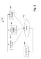
- FIG. 1is a schematic block diagram of an exposing system employed in accordance with an aspect of the present invention.
- FIG. 2illustrates measurements associated with determining critical dimensions in a latent image exposed in a photo resist in accordance with an aspect of the present invention.
- FIG. 3illustrates an unexposed resist and an exposed resist with a latent image exposed thereon, in accordance with an aspect of the present invention.
- FIG. 4illustrates critical dimension measurements employed in providing in situ control of integrated circuit manufacture, in accordance with an aspect of the present invention.
- FIG. 5is a schematic block diagram illustrating a critical dimension monitoring system providing in situ control of integrated circuit manufacture, in accordance with an aspect of the present invention.
- FIG. 6is schematic block diagram of an exposing system monitoring and control system employed with developing and/or post exposure baking control systems in accordance with an aspect of the present invention.
- FIG. 7is a partial schematic block diagram of a signature system being employed in connection with determining latent image properties in accordance with the an aspect of present invention.
- FIG. 8is a perspective illustration of a substrate, including photo resist, wherein the photo resist may have a latent image exposed thereon, the latent image including zero or more gratings, in accordance with an aspect of the present invention.
- FIG. 9is a representative three-dimensional grid map of a wafer illustrating signature measurements taken at grid blocks of the grid map in accordance with an aspect of the present invention.
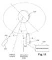
- FIG. 11illustrates an exemplary scatterometry system collecting reflected light.
- FIG. 13is a flow diagram illustrating one specific methodology for carrying out an aspect of the present invention.
- FIG. 14is a simplified perspective view of an incident light reflecting off a surface, in accordance with an aspect of the present invention.
- FIG. 15is a simplified perspective view of an incident light reflecting off a surface, in accordance with an aspect of the present invention.
- FIG. 16illustrates a complex reflected and refracted light produced when an incident light is directed onto a surface, in accordance with an aspect of the present invention.
- a componentis intended to refer to a computer-related entity, either hardware, a combination of hardware and software, software, or software in execution.
- a componentmay be, but is not limited to being, a process running on a processor, a processor, an object, an executable, a thread of execution, a program, a set of co-operating computers and/or processes and a computer.
- non-linear training systems/methodologiese.g., back propagation, Bayesian, fuzzy sets, non-linear regression, or other neural networking paradigms including mixture of experts, cerebella model arithmetic computer (CMACS), radial basis functions, directed search networks and function link networks may be employed).
- CMACScerebella model arithmetic computer
- the exposing system 100can also include a mask/reticle 140 , which can be employed to expose a pattern 170 on a wafer 160 .
- a mask/reticle 140which can be employed to expose a pattern 170 on a wafer 160 .
- Dimensions of features formed by exposing a pattern into a photo resist using the system 100can thus depend on the configuration of several cooperating elements (e.g., illumination source 110 , illumination filter 120 , lenses 130 and 150 , and reticle 140 ) during exposure. Thus, variations between exposures are possible. Conventionally, differences in properties of a latent image exposed into a photo resist may not be accounted for in subsequent manufacturing processes. But the present invention facilitates collecting information concerning the latent image formed in the photo resist, and thus facilitates adapting and controlling subsequent manufacturing processes (e.g., development, post exposure baking) based on such collected information.
- subsequent manufacturing processese.g., development, post exposure baking
- one or more of the illumination source 110 , the illumination modification filter 120 , the lens system 130 , the mask/reticle 140 and the lens system 150can be operably connected to an exposure driving system 180 .
- the exposure driving system 180can be operably connected to a scatterometry system 190 such that the scatterometry system 190 can collect signature data and provide feedback/feedforward information concerning the formation of the one or more patterns 170 on the wafer 160 .
- Such feedback/feedforward informationcan be employed to determine when to end the exposing process, for example.
- feedback/feedforward informationcan be employed in machine learning techniques to adapt future operation of the exposing system 100 .
- the signature datacan also be employed to control subsequent processes including, but not limited to, development and post exposure baking.
- the layer 200includes several features that have measurable dimensions. For example, dimensions including, but not limited to, the width 210 of a feature, the distance 220 between features, the slope 230 of the sides of a feature and the height 240 of a feature.
- the dimensionse.g., width 210 , spacing 220 , slope 230 , height 240 ) depend, at least in part, on the dimensions of features in a latent image exposed into a photo resist during a prior manufacturing process, which image was subsequently employed in development and baking.
- the unexposed resist 300typically has measured properties including, but not limited to, a width within predetermined width thresholds, a chemical composition within desired chemical composition ranges and a uniformity within predetermined uniformity thresholds.
- the prior manufacturing processesmay produce an unexposed resist 300 within all tolerances, the prior manufacturing processes may produce an unexposed resist 300 with different thickness, chemical compositions and/or uniformities due to variations in the manufacturing processes and/or variations in the wafer upon which the resist is deposited.
- unexposed resistsmay have different properties.
- the unexposed resist 300is exposed to a pattern that creates a latent image in the resist, the latent image may have different properties.
- the exposed resist 310may have a first feature 320 with a first depth and a second feature 330 with a second depth.
- Scatterometry techniquescan be employed to determine, for example, the depths of the features 320 and/or 330 and to determine what, if anything, those depths indicate concerning exposure.
- Scatterometry techniquescan also be employed to determine, based on the depths of the features 320 and/or 330 , for example, development times and/or temperatures and/or post exposure bake times and/or temperatures to be applied to the exposed resist 310 .
- different depthsmay generate different signatures that indicate one or more exposure results and which can thus be employed to generate feedback/feedforward information that can be employed to control post exposure steps and which can thus facilitate achieving desired critical dimensions.
- a first average depth and/or maximum and minimum depthmay indicate that a first development temperature should be applied for a first development time and that a first post exposure bake temperature should be applied for a first post exposure bake time while a second average depth and/or maximum and minimum depth may indicate that a second development temperature should be applied for a second development time and that a second post exposure bake temperature should be applied for a second post exposure bake time.
- the exposed resist 310may also have a third feature 340 and a fourth feature 350 whose sides are sloped.
- Scatterometry techniquescan be employed to determine what, if anything, the slopes indicate concerning exposure.
- scatterometry techniquescan be employed to determine, based on the slopes of the sides of the features 340 and/or 350 , for example, development times and/or temperatures and/or post exposure bake times and/or temperatures to be applied to the exposed resist 310 .
- different slopesmay generate different signatures that indicate one or more exposure results and which can thus be employed to generate feedback/feedforward information that can be employed to control post exposure processes and which can thus facilitate achieving desired critical dimensions.
- a first average slope and/or maximum and minimum slopemay indicate that a first development temperature should be applied for a first development time and that a first post exposure bake temperature should be applied for a first post exposure bake time while a second average slope and/or maximum and minimum slope may indicate that a second development temperature should be applied for a second development time and that a second post exposure bake temperature should be applied for a second post exposure bake time.
- the chemical composition of the exposed resist 310may also generate one or more signatures. Scatterometry techniques can be employed to determine what, if anything, the chemical composition indicates concerning exposure. Similarly, scatterometry techniques can be employed to determine, based on the chemical composition, development times and/or temperatures and/or post exposure bake times and/or temperatures to be applied to the exposed resist 310 . For example, different chemical compositions may generate different signatures that indicate one or more exposure results and which can thus be employed to generate feedback/feedforward information that can be employed to control post exposure processes and which can thus facilitate achieving desired critical dimensions.
- a first chemical compositionmay indicate that a first development temperature should be applied for a first development time and that a first post exposure bake temperature should be applied for a first post exposure bake time while a second chemical composition may indicate that a second development temperature should be applied for a second development time and that a second post exposure bake temperature should be applied for a second post exposure bake time.
- the wafermay include one or more features 410 , whose critical dimensions can be affected by exposure time and/or post exposure baking, for example.
- a first measurement for the length 420 of the feature 410may indicate that a first post exposure bake time should be employed in post exposure processes while a second measurement for the length 420 of the feature 410 may indicate that a second post exposure bake time should be employed in post exposure processes.
- a first measurement for the width 430 of the feature 410may indicate that a first post exposure bake time should be employed in post exposure processes while a second measurement for the width 430 of the feature 410 may indicate that a second post exposure bake time should be employed in post exposure processes.
- the critical dimension measurementse.g., length 420 , width 430
- the critical dimension measurements taken from the latent imagemay be correlated to facilitate producing feedback/feedforward information that can be employed to control post exposure processes.
- the area of the feature 410as determined by multiplying the length 420 by the width 430 may be employed in generating feedback/feedforward information that can be employed to control a post exposure development process.
- FIG. 5a simplified schematic block diagram illustrates a feed forward system 500 employed in controlling post exposure processes based, at least in part, on critical dimension information collected from a latent image on a wafer 540 .
- the system 500includes an exposing system 530 that is employed to expose a pattern on a photo-resist. Exposing the pattern produces a latent image on the wafer 540 , with features with measurable critical dimensions.
- the critical dimensionscan be measured through scatterometry means and fed into a critical dimension monitor 550 .
- the critical dimension monitor 550can then be employed to generate feed forward information that is employed in controlling a developing system 510 and/or a post exposure baking system 520 .
- FIG. 6a system 600 for monitoring exposure results of a pattern developed on a wafer 665 is shown.
- the latent imagemay include a grating 660 .
- the grating 660is formed on the wafer 665 , as part of the latent image exposed into the photo resist 675 , to facilitate analyzing critical dimensions in features in the latent image pattern exposed on the wafer 665 .
- the system 600further includes an exposing system 655 that is selectively controlled by the system 600 to facilitate controlling exposure of the pattern into the photo resist 675 .
- the wafer 665is supported on a chuck 670 .
- grating 660Although one grating 660 is illustrated, it is to be appreciated that a greater number of gratings may be employed by the present invention.
- the gratingscan be equal lines and/or spaces, and/or varying lines an/or spaces.
- linewidthranges from 1 ⁇ m to 50 nm.
- grating areais within a range of 100 ⁇ m ⁇ 100 ⁇ m to 10 ⁇ m ⁇ 10 ⁇ m so that a spot size of a light beam in accordance with the invention is smaller than the grating size. It is to be appreciated that the grating area and beam spot size can be suitably tailored and thus the subject invention should not be limited to any ranges noted herein as preferable.
- One or more light sources 635projects light onto respective portions of the wafer 665 .
- the wafer 665can be partitioned into one or more portions.
- the latent image exposed into the photo resist 675can be located in one or more of the portions.
- Each portion of the wafer 665can also have zero or more gratings 660 formed thereon.
- Light reflected, and/or passed through, the latent image and/or the gratings 660is collected by one or more light detecting components 640 , and processed by a signature system 630 to produce a signature that measures at least one parameter relating to the exposure of the latent image and/or gratings 660 .
- a signature associated with the latent image and/or one or more gratings 660may indicate that the exposing system 635 should terminate exposure of the pattern that is forming the latent image in the photo resist 675 .
- the reflected and/or passed through lightis processed with respect to the incident light in measuring the various parameters.
- the reflected and/or passed through or transmitted lightcan generate one or more signatures associated with the latent image and/or the one or more gratings 660 .
- the signaturescan be employed to generate feedback control information that can be employed to control the exposure via the exposure driving system.
- the signaturescan also be employed to generate feed forward information that can be employed by a developing system 645 and/or a baking system 650 .
- the signature system 630includes a scatterometry system 630 a. It is to be appreciated that any suitable scatterometry system may be employed to carry out the present invention and such systems are intended to fall within the scope of the claims appended hereto.
- a source of light 625(e.g., a laser) provides light to the one or more light sources 635 via the signature system 630 .
- the light source 625is a frequency stabilized laser, however, it will be appreciated that any laser or other light source (e.g., laser diode or helium neon (HeNe) gas laser) suitable for carrying out the present invention may be employed.
- One or more light detecting components 640e.g., photo detector, photo diodes) collect light reflecting from or passing through the latent image in the photo resist 675 and/or the one or more gratings 660 .
- a processor 605receives the measured data from the signature system 630 and determines whether to terminate exposure of the pattern that is forming the latent image in the photo resist 675 by the exposing system 655 based, at least in part, on comparing signatures measured from the latent image and/or the one or more gratings 660 formed in the photo resist 675 to desired signatures.
- the processor 605is operatively coupled to the signature system 630 and is programmed to control and operate the various components within the system 600 in order to carry out the various functions described herein.
- the processor, or CPU 605may be any of a plurality of processors, such as the AMD ATHLON and other similar and compatible processors.
- a memory 615which is operatively coupled to the processor 605 , is also included in the system 600 and can store program code executed by the processor 605 for carrying out operating functions of the system 600 as described herein.
- the memory 615also serves as a storage medium for temporarily storing information such as latent image signatures, grating signatures, exposure time, latent image signature tables, grating signature tables, component coordinate tables, latent image feature sizes, grating sizes, latent image feature shapes, grating shapes, scatterometry information, and other data that may be employed in carrying out the present invention.
- a power supply 620provides operating power to the system 600 .
- Any suitable power supply 620e.g., battery, line power
- the processor 605is also coupled to a developing/baking driving system 610 that drives a developing system 645 and/or a baking system 650 .
- the developing/baking driving system 610is controlled by the processor 605 to selectively cause the developing system 645 and/or the baking system 650 to change one or more properties including, but not limited to, development time, development temperature, post exposure bake time and post exposure bake temperature.
- the processor 605monitors the signatures associated with the latent image exposed in the photo resist 675 and the one or more gratings 660 and selectively controls the exposing system 655 . Similarly, the processor 605 monitors the signatures associated with the latent image exposed in the photo resist 675 and the one or more gratings 660 and generates feed forward information that can be employed to control the developing system 645 and/or the baking system 650 .
- the system 600provides for regulating how a wafer with a latent image exposed in the photo resist 675 will be developed and how a wafer with a latent image exposed in the photo resist 675 will be baked, which in turn improves fidelity of image transfer in a lithographic process. Improved image transfer fidelity facilitates achieving desired critical dimensions and thus smaller feature sizes and higher packing densities. Achieving substantially similar desired critical dimensions for different patterns on different layers improves IC quality, and facilitates higher speeds for such chips.
- FIG. 7illustrates a portion of a system 700 being employed to generate one or more signatures for a latent image and/or a grating 780 formed in photo resist 790 .
- a light source 730provides a light to one or more light emitters 740 that direct a light 760 incident to the surface of the photo resist 790 .
- the reflected light 770 from the surface of the photo resist 790will vary (e.g., variations in intensity and/or phase) in accordance with the critical dimensions achieved and/or chemical composition for the latent image and/or the grating 780 .
- One or more light detecting components 750collect the reflected light 770 , pass the collected light, and/or data concerning the collected light, to a signature system 720 , which processes the reflected light 770 and/or data concerning the reflected light 770 in accordance with suitable techniques (e.g., scatterometry, spectroscopic ellipsometry) to provide a processor 710 with grating signature data.
- the reflected light 770can be analyzed to generate one or more signatures that can be compared to one or more stored signatures to determine whether, for example, the latent image and/or the grating 780 has achieved desired critical dimensions and thus, whether exposure should be concluded.
- the reflected light 770can be analyzed to generate one or more signatures that can be compared to one or more stored signatures to generate, for example, feed forward information that can be employed to control post exposure processes including, but not limited to, a development process and a post exposure bake process.
- FIGS. 8-10a chuck 900 is shown in perspective supporting a wafer 910 whereupon a photo resist exposed with a latent image (including zero or more gratings (e.g., 660 , FIG. 6) is exposed.
- the wafer 910may be divided into a grid pattern as shown in FIG. 9 .
- Each grid block (XY) of the grid patterncorresponds to a particular portion of the wafer 910 , and each grid block has a portion of the latent image (including zero or more gratings (e.g., 660 , FIG. 6 )) associated with that grid block.
- Each portionis monitored individually for signatures generated by the latent image and or the one or more gratings (e.g., 660 , FIG. 6 ).
- one or more portions of the latent imageinclude one or more gratings (e.g., 660 , FIG. 6 )) in the respective portions of the wafer 910 (X 1 Y 1 . . . X 12 , Y 12 ) are being monitored for signatures using reflective and/or passed through light, a signature system and a processor.
- FIG. 9illustrates the wafer 910 being mapped (partitioned) into 144 grid block portions, the wafer 910 may be mapped with any suitable number of portions and any suitable number of gratings (e.g., 660 , FIG. 6) may be employed.
- a processormay determine that an undesirable exposure condition exists.
- a processormay generate feed forward information to provide to post exposure processes including, but not limited to, developing processes and baking processes.
- the processormay control systems including, but not limited to, an exposing system, a development system and a baking system.
- the exposing systemmay be driven so as to maintain, terminate, and/or adjust exposure.
- the development systemmay be driven so as to establish, maintain, and/or adjust development properties including, but not limited to, time, temperature and atmosphere.
- the baking systemmay be driven so as to establish, maintain, and/or adjust baking properties including, but not limited to, time and temperature.
- FIG. 10illustrates a table of expected and unexpected signatures. It can be seen that all the signatures are expected except a signature for grid X 7 Y 6 .
- the set of depicted signaturescan be analyzed collectively as a master signature, can be analyzed in subsets to evaluate, for example, intermediate exposure results and/or may be analyzed individually to determine whether an acceptable exposure has occurred.
- the analysis of the signaturescan be employed to control systems including, but not limited to, an exposing driving system, a development system and a baking system, so that more precise critical dimensions may be achieved.
- FIG. 11illustrates an exemplary scatterometry system collecting reflected light.
- Light from a laser 1200is brought to focus in any suitable well-known manner to form a beam 1202 .
- a samplesuch as a wafer 1204 is placed in the path of the beam 1202 and a photo detector or photo multiplier 1206 of any suitable well-known construction. Different detector methods may be employed to determine the scattered power.
- the photo detector or photo multiplier 1206may be mounted on a rotation stage 1208 of any suitable well-known design.
- a microprocessor 1210of any suitable well-known design, may be used to process detector readouts, including, but not limited to, angular locations of different diffracted orders leading to diffraction grating pitches being calculated.
- light reflected from the sample 1204may be accurately measured.
- the various blocksmay be implemented via software, hardware a combination thereof or any suitable means (e.g., device, system, process, component) for carrying out the functionality associated with the blocks. It is also to be appreciated that the blocks are merely to illustrate certain aspects of the present invention in a simplified form and that these aspects may be illustrated via a lesser and/or greater number of blocks.
- FIG. 12is a flow diagram illustrating a methodology 1400 for carrying out aspects of the present invention.
- initializationscan include, but are not limited to, acquiring memory, acquiring resources, establishing data communications, establishing variables and instantiating one or more objects.
- a patternis exposed onto a photo resist. Exposing the pattern onto the photo resist will cause a latent image to begin to form on the photo resist.
- scatterometry techniquesare employed to analyze the emerging latent image.
- a determinationis made concerning whether exposure of the pattern has completed. For example, properties including, but not limited to the depth, width, slope and chemical composition of features in the latent image can be analyzed. If the determination at 1440 is NO, then at 1450 an estimated remaining exposure time can be calculated, and the process can continue at 1420 .
- properties associated with a post exposure development processcan be calculated. For example, properties including, but not limited to, development time, development temperature and development atmosphere composition can be determined. Information concerning such properties can be fed forward to a subsequent development process, thus facilitating achieving desired critical dimensions with resulting improvements in chip quality.
- the post exposure development processcan be adapted in reaction to scatterometry measurements associated with the exposure process, facilitating improvements in chip quality, and providing an improvement over conventional systems.
- properties associated with a post exposure baking processcan be calculated. For example, properties including, but not limited to, baking time, baking temperature and baking atmosphere composition can be determined. Information concerning such properties can be fed forward to a subsequent baking process, thus facilitating achieving desired critical dimensions with resulting improvements in chip quality.
- FIG. 13is a flow diagram illustrating a methodology 1500 for carrying out aspects of the present invention.
- general initializationsare performed. Such initializations can include, but are not limited to, acquiring memory, acquiring resources, establishing data communications, establishing variables and instantiating one or more objects.
- a grid mapcomprising a plurality of grid blocks “XY” is generated.
- one or more gratingsare exposed and begin forming part of a latent image on a photo resist. Zero or more gratings may be exposed in each of the grid blocks “XY”.
- scatterometry techniquesare employed to measure properties of the gratings of 1515 .
- the scatterometry techniques of 1520can include, but are not limited to, analyzing grating signatures.
- a simple table lookup value, or “proceed as normal” signalcan be fed forward to post exposure developing and/or baking processes.
- a simple table lookup value, or “proceed as normal” signalcan be fed forward to post exposure developing and/or baking processes.
- the determination at 1535is YES, that an unexpected signature was encountered, then at 1550 , techniques for computing post exposure developer properties when the latent image has dimensions and/or properties outside expected ranges and/or tolerances, as indicated by one or more signatures read from one or more gratings, can be employed. For example, data generated by sophisticated modeling techniques can be fed forward to a post exposure development process to facilitate achieving desired critical dimensions even though exposure generated unexpected properties and/or dimensions.
- techniques for computing post exposure baking properties when the latent image has dimensions and/or properties outside expected ranges and/or tolerances, as indicated by one or more signatures read from one or more gratingscan be employed.
- data generated by sophisticated neural network processing techniquescan be fed forward to a post exposure baking process to facilitate achieving desired critical dimensions even though exposure generated unexpected properties and/or dimensions.
- Scatterometryis a technique for extracting information about a surface upon which an incident light has been directed.
- Information concerning propertiesincluding, but not limited to, dishing, erosion, profile, chemical composition, thickness of thin films and critical dimensions of features present on a surface such as a wafer can be extracted.
- the informationcan be extracted by comparing the phase and/or intensity of the light directed onto the surface with phase and/or intensity signals of a complex reflected and/or diffracted light resulting from the incident light reflecting from and/or diffracting through the surface upon which the incident light was directed.
- the intensity and/or the phase of the reflected and/or diffracted lightwill change based on properties of the surface upon which the light is directed.
- Such propertiesinclude, but are not limited to, the chemical properties of the surface, the planarity of the surface, features on the surface, voids in the surface, and the number and/or type of layers beneath the surface.
- the signal (signature) librarycan be constructed from observed intensity/phase signatures and/or signatures generated by modeling and simulation.
- a first feature on a waferwhen exposed to a first incident light of known intensity, wavelength and phase, a first feature on a wafer can generate a first phase/intensity signature.
- a second feature on a waferwhen exposed to the first incident light of known intensity, wavelength and phase, a second feature on a wafer can generate a second phase/intensity signature.
- a line of a first widthmay generate a first signature while a line of a second width may generate a second signature.
- Observed signaturescan be combined with simulated and modeled signatures to form the signal (signature) library.
- Simulation and modelingcan be employed to produce signatures against which measured phase/intensity signatures can be matched.
- simulation, modeling and observed signaturesare stored in a signal (signature) library containing over three hundred thousand phase/intensity signatures.
- signalsignature
- the phase/intensity signalscan be pattern matched, for example, to the library of signals to determine whether the signals correspond to a stored signature.
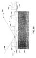
- an incident light 1602is directed at a surface 1600 , upon which one or more features 1606 may exist.
- the incident light 1602is reflected as reflected light 1604 .
- the properties of the surface 1600including but not limited to, thickness, uniformity, planarity, chemical composition and the presence of features, can affect the reflected light 1604 .
- the features 1606are raised upon the surface 1600 .
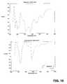
- the phase and intensity of the reflected light 1604can be measured and plotted, as shown, for example, in FIG. 19 .
- the phase 2100 of the reflected light 1604can be plotted, as can the intensity 2110 of the reflected light 1604 .
- Such plotscan be employed to compare measured signals with signatures stored in a signature library using techniques like pattern matching, for example.
- an incident light 1712is directed onto a surface 1710 upon which one or more depressions 1716 appear.
- the incident light 1712is reflected as reflected light 1514 .
- the one or more depressions 1716affect an incident beam.
- scatterometrycan be employed to measure features appearing on a surface, features appearing in a surface, and properties of a surface itself, regardless of features.
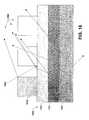
- the reflection and refraction of the incident light 1840can be affected by factors including, but not limited to, the presence of one or more features 1828 , and the composition of the substrate 1820 upon which the features 1828 reside.
- properties of the substrate 1820including, but not limited to the thickness of a layer 1822 , the chemical composition of the layer 1822 , the opacity and/or reflectivity of the layer 1822 , the thickness of a layer 1824 , the chemical composition of the layer 1824 , the opacity and/or reflectivity of the layer 1824 , the thickness of a layer 1826 , the chemical composition of the layer 1826 , and the opacity and/or reflectivity of the layer 1826 can affect the reflection and/or refraction of the incident light 1840 .
- a complex reflected and/or refracted light 1842may result from the incident light 1840 interacting with the features 1828 , and/or the layers 1822 , 1824 and 1826 .
- three layers 1822 , 1824 and 1826are illustrated, it is to be appreciated that a substrate can be formed of a greater or lesser number of such layers.
- the substrate 1920can be formed of one or more layers 1922 , 1924 and 1926 .
- the phase 1950 of the reflected and/or refracted light 1942can depend, at least in part, on the thickness of a layer, for example, the layer 1924 .
- the phase 2052 of a reflected light 2042differs from the phase 1950 due, at least in part, to the different thickness of the layer 2024 in FIG. 18 from the thickness of the layer 1924 in FIG. 17 .
- scatterometryis a technique that can be employed to extract information about a surface upon which an incident light has been directed.
- the informationcan be extracted by analyzing phase and/or intensity signals of a complex reflected and/or diffracted light.
- the intensity and/or the phase of the reflected and/or diffracted lightwill change based on properties of the surface upon which the light is directed, resulting in substantially unique signatures that can be analyzed to determine one or more properties of the surface upon which the incident light was directed.
Landscapes
- Physics & Mathematics (AREA)
- General Physics & Mathematics (AREA)
- Exposure And Positioning Against Photoresist Photosensitive Materials (AREA)
- Investigating Or Analysing Materials By Optical Means (AREA)
Abstract
Description
Claims (11)
Priority Applications (5)
| Application Number | Priority Date | Filing Date | Title |
|---|---|---|---|
| US09/893,807US6561706B2 (en) | 2001-06-28 | 2001-06-28 | Critical dimension monitoring from latent image |
| PCT/US2002/003020WO2003003123A2 (en) | 2001-06-28 | 2002-01-31 | Critical dimension monitoring from latent image |
| EP02704323AEP1417540A2 (en) | 2001-06-28 | 2002-01-31 | Critical dimension monitoring from latent image |
| AU2002238013AAU2002238013A1 (en) | 2001-06-28 | 2002-01-31 | Critical dimension monitoring from latent image |
| TW091112605ATWI265557B (en) | 2001-06-28 | 2002-06-11 | Critical dimension monitoring from latent image |
Applications Claiming Priority (1)
| Application Number | Priority Date | Filing Date | Title |
|---|---|---|---|
| US09/893,807US6561706B2 (en) | 2001-06-28 | 2001-06-28 | Critical dimension monitoring from latent image |
Publications (2)
| Publication Number | Publication Date |
|---|---|
| US20030002878A1 US20030002878A1 (en) | 2003-01-02 |
| US6561706B2true US6561706B2 (en) | 2003-05-13 |
Family
ID=25402129
Family Applications (1)
| Application Number | Title | Priority Date | Filing Date |
|---|---|---|---|
| US09/893,807Expired - LifetimeUS6561706B2 (en) | 2001-06-28 | 2001-06-28 | Critical dimension monitoring from latent image |
Country Status (5)
| Country | Link |
|---|---|
| US (1) | US6561706B2 (en) |
| EP (1) | EP1417540A2 (en) |
| AU (1) | AU2002238013A1 (en) |
| TW (1) | TWI265557B (en) |
| WO (1) | WO2003003123A2 (en) |
Cited By (55)
| Publication number | Priority date | Publication date | Assignee | Title |
|---|---|---|---|---|
| US20020094496A1 (en)* | 2000-07-17 | 2002-07-18 | Choi Byung J. | Method and system of automatic fluid dispensing for imprint lithography processes |
| US20020093122A1 (en)* | 2000-08-01 | 2002-07-18 | Choi Byung J. | Methods for high-precision gap and orientation sensing between a transparent template and substrate for imprint lithography |
| US20020150398A1 (en)* | 2000-08-21 | 2002-10-17 | Choi Byung J. | Flexure based macro motion translation stage |
| US20030205657A1 (en)* | 2002-05-01 | 2003-11-06 | Voisin Ronald D. | Methods of manufacturing a lithography template |
| US20030215577A1 (en)* | 2002-05-16 | 2003-11-20 | Willson Carlton Grant | Method and system for fabricating nanoscale patterns in light curable compositions using an electric field |
| US20030235787A1 (en)* | 2002-06-24 | 2003-12-25 | Watts Michael P.C. | Low viscosity high resolution patterning material |
| US20040009673A1 (en)* | 2002-07-11 | 2004-01-15 | Sreenivasan Sidlgata V. | Method and system for imprint lithography using an electric field |
| US20040022888A1 (en)* | 2002-08-01 | 2004-02-05 | Sreenivasan Sidlgata V. | Alignment systems for imprint lithography |
| US20040038552A1 (en)* | 2002-08-23 | 2004-02-26 | Watts Michael P.C. | Method for fabricating bulbous-shaped vias |
| US20040053146A1 (en)* | 2000-07-16 | 2004-03-18 | University Of Texas System Board Of Regents, Ut System | Method of varying template dimensions to achieve alignment during imprint lithography |
| US6721046B1 (en)* | 2001-07-12 | 2004-04-13 | Advanced Micro Devices, Inc. | Monitoring of concentration of nitrogen in nitrided gate oxides, and gate oxide interfaces |
| US6727995B1 (en)* | 2001-07-12 | 2004-04-27 | Advanced Micro Devices, Inc. | Gate oxide thickness measurement and control using scatterometry |
| US6742168B1 (en)* | 2002-03-19 | 2004-05-25 | Advanced Micro Devices, Inc. | Method and structure for calibrating scatterometry-based metrology tool used to measure dimensions of features on a semiconductor device |
| US20040104641A1 (en)* | 1999-10-29 | 2004-06-03 | University Of Texas System | Method of separating a template from a substrate during imprint lithography |
| US20040112861A1 (en)* | 2002-12-11 | 2004-06-17 | Molecular Imprints, Inc. | Method for modulating shapes of substrates |
| US20040112153A1 (en)* | 2002-12-12 | 2004-06-17 | Molecular Imprints, Inc. | Method and system for determining characteristics of substrates employing fluid geometries |
| US6770852B1 (en)* | 2003-02-27 | 2004-08-03 | Lam Research Corporation | Critical dimension variation compensation across a wafer by means of local wafer temperature control |
| US20040170771A1 (en)* | 2000-10-12 | 2004-09-02 | Board Of Regents, The University Of Texas System | Method of creating a dispersion of a liquid on a substrate |
| US20040170770A1 (en)* | 2003-02-27 | 2004-09-02 | Molecular Imprints, Inc. | Method to reduce adhesion between a polymerizable layer and a substrate employing a fluorine-containing layer |
| US20040188381A1 (en)* | 2003-03-25 | 2004-09-30 | Molecular Imprints, Inc. | Positive tone bi-layer imprint lithography method |
| US6809824B1 (en)* | 2001-11-30 | 2004-10-26 | Lsi Logic Corporation | Alignment process for integrated circuit structures on semiconductor substrate using scatterometry measurements of latent images in spaced apart test fields on substrate |
| US20040211754A1 (en)* | 2003-04-25 | 2004-10-28 | Molecular Imprints, Inc. | Method of forming stepped structures employing imprint lithography |
| US20050037143A1 (en)* | 2000-07-18 | 2005-02-17 | Chou Stephen Y. | Imprint lithography with improved monitoring and control and apparatus therefor |
| US20050059251A1 (en)* | 2003-09-12 | 2005-03-17 | Taiwan Semicondutor Manufacturing Co. | Constant and reducible hole bottom CD in variable post-CMP thickness and after-development-inspection CD |
| US20050072755A1 (en)* | 2003-10-02 | 2005-04-07 | University Of Texas System Board Of Regents | Single phase fluid imprint lithography method |
| US6900881B2 (en) | 2002-07-11 | 2005-05-31 | Molecular Imprints, Inc. | Step and repeat imprint lithography systems |
| US6916584B2 (en) | 2002-08-01 | 2005-07-12 | Molecular Imprints, Inc. | Alignment methods for imprint lithography |
| US6926929B2 (en) | 2002-07-09 | 2005-08-09 | Molecular Imprints, Inc. | System and method for dispensing liquids |
| US6929762B2 (en) | 2002-11-13 | 2005-08-16 | Molecular Imprints, Inc. | Method of reducing pattern distortions during imprint lithography processes |
| US6932934B2 (en) | 2002-07-11 | 2005-08-23 | Molecular Imprints, Inc. | Formation of discontinuous films during an imprint lithography process |
| US20050185169A1 (en)* | 2004-02-19 | 2005-08-25 | Molecular Imprints, Inc. | Method and system to measure characteristics of a film disposed on a substrate |
| US7019819B2 (en) | 2002-11-13 | 2006-03-28 | Molecular Imprints, Inc. | Chucking system for modulating shapes of substrates |
| US7027156B2 (en) | 2002-08-01 | 2006-04-11 | Molecular Imprints, Inc. | Scatterometry alignment for imprint lithography |
| US20060094131A1 (en)* | 2004-11-02 | 2006-05-04 | Taiwan Semiconductor Manufacturing Company, Ltd. | System and method for critical dimension control in semiconductor manufacturing |
| US20060145398A1 (en)* | 2004-12-30 | 2006-07-06 | Board Of Regents, The University Of Texas System | Release layer comprising diamond-like carbon (DLC) or doped DLC with tunable composition for imprint lithography templates and contact masks |
| US7077992B2 (en) | 2002-07-11 | 2006-07-18 | Molecular Imprints, Inc. | Step and repeat imprint lithography processes |
| US7122079B2 (en) | 2004-02-27 | 2006-10-17 | Molecular Imprints, Inc. | Composition for an etching mask comprising a silicon-containing material |
| US7136150B2 (en) | 2003-09-25 | 2006-11-14 | Molecular Imprints, Inc. | Imprint lithography template having opaque alignment marks |
| US7157036B2 (en) | 2003-06-17 | 2007-01-02 | Molecular Imprints, Inc | Method to reduce adhesion between a conformable region and a pattern of a mold |
| US20070231935A1 (en)* | 2006-03-29 | 2007-10-04 | Taiwan Semiconductor Manufacturing Company, Ltd. | Novel critical dimension (cd) control by spectrum metrology |
| US7334202B1 (en)* | 2005-06-03 | 2008-02-19 | Advanced Micro Devices, Inc. | Optimizing critical dimension uniformity utilizing a resist bake plate simulator |
| US20080141862A1 (en)* | 2003-10-02 | 2008-06-19 | Molecular Imprints, Inc. | Single Phase Fluid Imprint Lithography Method |
| US7405032B1 (en)* | 2003-08-21 | 2008-07-29 | Advanced Micro Devices, Inc. | Combination of non-lithographic shrink techniques and trim process for gate formation and line-edge roughness reduction |
| US20080185538A1 (en)* | 2007-02-01 | 2008-08-07 | Nuflare Technology, Inc. | Pattern forming method, charged particle beam writing apparatus, and recording medium on which program is recorded |
| US20090169662A1 (en)* | 2004-11-30 | 2009-07-02 | Molecular Imprints, Inc. | Enhanced Multi Channel Alignment |
| US7630067B2 (en) | 2004-11-30 | 2009-12-08 | Molecular Imprints, Inc. | Interferometric analysis method for the manufacture of nano-scale devices |
| US20090324056A1 (en)* | 2006-04-21 | 2009-12-31 | Rudolph Technologies, Inc. | Polarization imaging |
| US20100209830A1 (en)* | 2009-02-13 | 2010-08-19 | Tokyo Electron Limited | Multi-Pitch Scatterometry Targets |
| WO2010096407A1 (en)* | 2009-02-18 | 2010-08-26 | Rudolph Technologies, Inc. | Polarization imaging |
| US7785526B2 (en) | 2004-07-20 | 2010-08-31 | Molecular Imprints, Inc. | Imprint alignment method, system, and template |
| US7906180B2 (en) | 2004-02-27 | 2011-03-15 | Molecular Imprints, Inc. | Composition for an etching mask comprising a silicon-containing material |
| US8076386B2 (en) | 2004-02-23 | 2011-12-13 | Molecular Imprints, Inc. | Materials for imprint lithography |
| US20130004057A1 (en)* | 2003-11-20 | 2013-01-03 | Kaoru Sakai | Method and apparatus for inspecting pattern defects |
| US8349241B2 (en) | 2002-10-04 | 2013-01-08 | Molecular Imprints, Inc. | Method to arrange features on a substrate to replicate features having minimal dimensional variability |
| US10409169B2 (en) | 2016-06-28 | 2019-09-10 | Samsung Electronics Co., Ltd. | Methods of manufacturing photomasks, methods of inspecting photomasks, and methods of manufacturing semiconductor devices |
Families Citing this family (6)
| Publication number | Priority date | Publication date | Assignee | Title |
|---|---|---|---|---|
| US7449348B1 (en)* | 2004-06-02 | 2008-11-11 | Advanced Micro Devices, Inc. | Feedback control of imprint mask feature profile using scatterometry and spacer etchback |
| US7566181B2 (en)* | 2004-09-01 | 2009-07-28 | Tokyo Electron Limited | Controlling critical dimensions of structures formed on a wafer in semiconductor processing |
| US7099789B1 (en)* | 2004-09-02 | 2006-08-29 | Advanced Micro Devices, Inc. | Characterizing distribution signatures in integrated circuit technology |
| US7460251B2 (en)* | 2005-10-05 | 2008-12-02 | Taiwan Semiconductor Manufacturing Co. | Dimension monitoring method and system |
| EP3495888A1 (en)* | 2017-12-06 | 2019-06-12 | ASML Netherlands B.V. | Method for controlling a lithographic apparatus and associated apparatuses |
| US10579764B2 (en)* | 2018-06-06 | 2020-03-03 | International Business Machines Corporation | Co-modeling post-lithography critical dimensions and post-etch critical dimensions with multi-task neural networks |
Citations (8)
| Publication number | Priority date | Publication date | Assignee | Title |
|---|---|---|---|---|
| US5393624A (en)* | 1988-07-29 | 1995-02-28 | Tokyo Electron Limited | Method and apparatus for manufacturing a semiconductor device |
| US5867276A (en)* | 1997-03-07 | 1999-02-02 | Bio-Rad Laboratories, Inc. | Method for broad wavelength scatterometry |
| US5923423A (en)* | 1996-09-12 | 1999-07-13 | Sentec Corporation | Heterodyne scatterometer for detecting and analyzing wafer surface defects |
| US6100985A (en)* | 1998-03-18 | 2000-08-08 | Nova Measuring Instruments, Ltd. | Method and apparatus for measurements of patterned structures |
| US6259521B1 (en)* | 1999-10-05 | 2001-07-10 | Advanced Micro Devices, Inc. | Method and apparatus for controlling photolithography parameters based on photoresist images |
| US6266125B1 (en)* | 1998-05-25 | 2001-07-24 | Tokyo Electron Limited | Resist processing method and apparatus |
| US6388253B1 (en)* | 1999-06-29 | 2002-05-14 | Applied Materials, Inc. | Integrated critical dimension control for semiconductor device manufacturing |
| US6424417B1 (en)* | 1998-06-14 | 2002-07-23 | Nova Measuring Instruments Ltd. | Method and system for controlling the photolithography process |
Family Cites Families (4)
| Publication number | Priority date | Publication date | Assignee | Title |
|---|---|---|---|---|
| JPS60249327A (en)* | 1984-05-25 | 1985-12-10 | Hitachi Ltd | Method of detecting resist pattern |
| DE69231715D1 (en) | 1991-03-04 | 2001-04-12 | At & T Corp | Manufacturing process of semiconductor integrated circuits using latent images |
| BE1006067A3 (en) | 1992-07-01 | 1994-05-03 | Imec Inter Uni Micro Electr | OPTICAL SYSTEM FOR REPRESENTING A MASK PATTERN IN A photosensitive layer. |
| TW389949B (en) | 1997-01-30 | 2000-05-11 | Tokyo Electron Ltd | Method and apparatus for coating and development of the photo-resist solution |
- 2001
- 2001-06-28USUS09/893,807patent/US6561706B2/ennot_activeExpired - Lifetime
- 2002
- 2002-01-31AUAU2002238013Apatent/AU2002238013A1/ennot_activeAbandoned
- 2002-01-31WOPCT/US2002/003020patent/WO2003003123A2/ennot_activeApplication Discontinuation
- 2002-01-31EPEP02704323Apatent/EP1417540A2/ennot_activeWithdrawn
- 2002-06-11TWTW091112605Apatent/TWI265557B/ennot_activeIP Right Cessation
Patent Citations (8)
| Publication number | Priority date | Publication date | Assignee | Title |
|---|---|---|---|---|
| US5393624A (en)* | 1988-07-29 | 1995-02-28 | Tokyo Electron Limited | Method and apparatus for manufacturing a semiconductor device |
| US5923423A (en)* | 1996-09-12 | 1999-07-13 | Sentec Corporation | Heterodyne scatterometer for detecting and analyzing wafer surface defects |
| US5867276A (en)* | 1997-03-07 | 1999-02-02 | Bio-Rad Laboratories, Inc. | Method for broad wavelength scatterometry |
| US6100985A (en)* | 1998-03-18 | 2000-08-08 | Nova Measuring Instruments, Ltd. | Method and apparatus for measurements of patterned structures |
| US6266125B1 (en)* | 1998-05-25 | 2001-07-24 | Tokyo Electron Limited | Resist processing method and apparatus |
| US6424417B1 (en)* | 1998-06-14 | 2002-07-23 | Nova Measuring Instruments Ltd. | Method and system for controlling the photolithography process |
| US6388253B1 (en)* | 1999-06-29 | 2002-05-14 | Applied Materials, Inc. | Integrated critical dimension control for semiconductor device manufacturing |
| US6259521B1 (en)* | 1999-10-05 | 2001-07-10 | Advanced Micro Devices, Inc. | Method and apparatus for controlling photolithography parameters based on photoresist images |
Cited By (97)
| Publication number | Priority date | Publication date | Assignee | Title |
|---|---|---|---|---|
| US20040104641A1 (en)* | 1999-10-29 | 2004-06-03 | University Of Texas System | Method of separating a template from a substrate during imprint lithography |
| US6873087B1 (en)* | 1999-10-29 | 2005-03-29 | Board Of Regents, The University Of Texas System | High precision orientation alignment and gap control stages for imprint lithography processes |
| US7060402B2 (en) | 1999-10-29 | 2006-06-13 | Board Of Regents, The University Of Texas System | Method of orientating a template with respect to a substrate in response to a force exerted on the template |
| US20050089774A1 (en)* | 1999-10-29 | 2005-04-28 | Board Of Regents, The University Of Texas System | Method to control the relative position between a body and a surface |
| US7098572B2 (en) | 1999-10-29 | 2006-08-29 | Board Of Regents, The University Of Texas System | Apparatus to control displacement of a body spaced-apart from a surface |
| US6955868B2 (en) | 1999-10-29 | 2005-10-18 | Board Of Regents, The University Of Texas System | Method to control the relative position between a body and a surface |
| US20040168588A1 (en)* | 1999-10-29 | 2004-09-02 | Board Of Regents, The University Of Texas System | Method of orientating a template with respect to a substrate in response to a force exerted on the template |
| US20040189996A1 (en)* | 2000-07-16 | 2004-09-30 | Board Of Regents, The University Of Texas System | Method of aligning a template with a substrate employing moire patterns |
| US20040053146A1 (en)* | 2000-07-16 | 2004-03-18 | University Of Texas System Board Of Regents, Ut System | Method of varying template dimensions to achieve alignment during imprint lithography |
| US6842229B2 (en) | 2000-07-16 | 2005-01-11 | Board Of Regents, The University Of Texas System | Imprint lithography template comprising alignment marks |
| US6916585B2 (en) | 2000-07-16 | 2005-07-12 | Board Of Regents, The University Of Texas Systems | Method of varying template dimensions to achieve alignment during imprint lithography |
| US6921615B2 (en) | 2000-07-16 | 2005-07-26 | Board Of Regents, The University Of Texas System | High-resolution overlay alignment methods for imprint lithography |
| US6902853B2 (en) | 2000-07-16 | 2005-06-07 | Board Of Regents, The University Of Texas System | Dual wavelength method of determining a relative position of a substrate and a template |
| US20040209177A1 (en)* | 2000-07-16 | 2004-10-21 | Board Of Regents, The University Of Texas System | Dual wavelength method of determining a relative position of a substrate and a template |
| US6986975B2 (en) | 2000-07-16 | 2006-01-17 | Board Of Regents, The University Of Texas System | Method of aligning a template with a substrate employing moire patterns |
| US6919152B2 (en) | 2000-07-16 | 2005-07-19 | Board Of Regents, The University Of Texas System | High resolution overlay alignment systems for imprint lithography |
| US20020094496A1 (en)* | 2000-07-17 | 2002-07-18 | Choi Byung J. | Method and system of automatic fluid dispensing for imprint lithography processes |
| US9223202B2 (en) | 2000-07-17 | 2015-12-29 | Board Of Regents, The University Of Texas System | Method of automatic fluid dispensing for imprint lithography processes |
| US20050037143A1 (en)* | 2000-07-18 | 2005-02-17 | Chou Stephen Y. | Imprint lithography with improved monitoring and control and apparatus therefor |
| US6954275B2 (en) | 2000-08-01 | 2005-10-11 | Boards Of Regents, The University Of Texas System | Methods for high-precision gap and orientation sensing between a transparent template and substrate for imprint lithography |
| US20020093122A1 (en)* | 2000-08-01 | 2002-07-18 | Choi Byung J. | Methods for high-precision gap and orientation sensing between a transparent template and substrate for imprint lithography |
| US20020150398A1 (en)* | 2000-08-21 | 2002-10-17 | Choi Byung J. | Flexure based macro motion translation stage |
| US8016277B2 (en) | 2000-08-21 | 2011-09-13 | Board Of Regents, The University Of Texas System | Flexure based macro motion translation stage |
| US20040170771A1 (en)* | 2000-10-12 | 2004-09-02 | Board Of Regents, The University Of Texas System | Method of creating a dispersion of a liquid on a substrate |
| US7060324B2 (en) | 2000-10-12 | 2006-06-13 | Board Of Regents, The University Of Texas System | Method of creating a dispersion of a liquid on a substrate |
| US6727995B1 (en)* | 2001-07-12 | 2004-04-27 | Advanced Micro Devices, Inc. | Gate oxide thickness measurement and control using scatterometry |
| US6721046B1 (en)* | 2001-07-12 | 2004-04-13 | Advanced Micro Devices, Inc. | Monitoring of concentration of nitrogen in nitrided gate oxides, and gate oxide interfaces |
| US6809824B1 (en)* | 2001-11-30 | 2004-10-26 | Lsi Logic Corporation | Alignment process for integrated circuit structures on semiconductor substrate using scatterometry measurements of latent images in spaced apart test fields on substrate |
| US6742168B1 (en)* | 2002-03-19 | 2004-05-25 | Advanced Micro Devices, Inc. | Method and structure for calibrating scatterometry-based metrology tool used to measure dimensions of features on a semiconductor device |
| US20030205657A1 (en)* | 2002-05-01 | 2003-11-06 | Voisin Ronald D. | Methods of manufacturing a lithography template |
| US7037639B2 (en) | 2002-05-01 | 2006-05-02 | Molecular Imprints, Inc. | Methods of manufacturing a lithography template |
| US20030215577A1 (en)* | 2002-05-16 | 2003-11-20 | Willson Carlton Grant | Method and system for fabricating nanoscale patterns in light curable compositions using an electric field |
| US6964793B2 (en) | 2002-05-16 | 2005-11-15 | Board Of Regents, The University Of Texas System | Method for fabricating nanoscale patterns in light curable compositions using an electric field |
| US20030235787A1 (en)* | 2002-06-24 | 2003-12-25 | Watts Michael P.C. | Low viscosity high resolution patterning material |
| US6926929B2 (en) | 2002-07-09 | 2005-08-09 | Molecular Imprints, Inc. | System and method for dispensing liquids |
| US7077992B2 (en) | 2002-07-11 | 2006-07-18 | Molecular Imprints, Inc. | Step and repeat imprint lithography processes |
| US6900881B2 (en) | 2002-07-11 | 2005-05-31 | Molecular Imprints, Inc. | Step and repeat imprint lithography systems |
| US6908861B2 (en) | 2002-07-11 | 2005-06-21 | Molecular Imprints, Inc. | Method for imprint lithography using an electric field |
| US20040009673A1 (en)* | 2002-07-11 | 2004-01-15 | Sreenivasan Sidlgata V. | Method and system for imprint lithography using an electric field |
| US6932934B2 (en) | 2002-07-11 | 2005-08-23 | Molecular Imprints, Inc. | Formation of discontinuous films during an imprint lithography process |
| US20040022888A1 (en)* | 2002-08-01 | 2004-02-05 | Sreenivasan Sidlgata V. | Alignment systems for imprint lithography |
| US7070405B2 (en) | 2002-08-01 | 2006-07-04 | Molecular Imprints, Inc. | Alignment systems for imprint lithography |
| US7027156B2 (en) | 2002-08-01 | 2006-04-11 | Molecular Imprints, Inc. | Scatterometry alignment for imprint lithography |
| US6916584B2 (en) | 2002-08-01 | 2005-07-12 | Molecular Imprints, Inc. | Alignment methods for imprint lithography |
| US20040038552A1 (en)* | 2002-08-23 | 2004-02-26 | Watts Michael P.C. | Method for fabricating bulbous-shaped vias |
| US7071088B2 (en) | 2002-08-23 | 2006-07-04 | Molecular Imprints, Inc. | Method for fabricating bulbous-shaped vias |
| US8349241B2 (en) | 2002-10-04 | 2013-01-08 | Molecular Imprints, Inc. | Method to arrange features on a substrate to replicate features having minimal dimensional variability |
| US6929762B2 (en) | 2002-11-13 | 2005-08-16 | Molecular Imprints, Inc. | Method of reducing pattern distortions during imprint lithography processes |
| US7019819B2 (en) | 2002-11-13 | 2006-03-28 | Molecular Imprints, Inc. | Chucking system for modulating shapes of substrates |
| US6980282B2 (en) | 2002-12-11 | 2005-12-27 | Molecular Imprints, Inc. | Method for modulating shapes of substrates |
| US20040112861A1 (en)* | 2002-12-11 | 2004-06-17 | Molecular Imprints, Inc. | Method for modulating shapes of substrates |
| US20040112153A1 (en)* | 2002-12-12 | 2004-06-17 | Molecular Imprints, Inc. | Method and system for determining characteristics of substrates employing fluid geometries |
| US6871558B2 (en) | 2002-12-12 | 2005-03-29 | Molecular Imprints, Inc. | Method for determining characteristics of substrate employing fluid geometries |
| US6990870B2 (en) | 2002-12-12 | 2006-01-31 | Molecular Imprints, Inc. | System for determining characteristics of substrates employing fluid geometries |
| US20050028618A1 (en)* | 2002-12-12 | 2005-02-10 | Molecular Imprints, Inc. | System for determining characteristics of substrates employing fluid geometries |
| US6770852B1 (en)* | 2003-02-27 | 2004-08-03 | Lam Research Corporation | Critical dimension variation compensation across a wafer by means of local wafer temperature control |
| US7452574B2 (en) | 2003-02-27 | 2008-11-18 | Molecular Imprints, Inc. | Method to reduce adhesion between a polymerizable layer and a substrate employing a fluorine-containing layer |
| US20040170770A1 (en)* | 2003-02-27 | 2004-09-02 | Molecular Imprints, Inc. | Method to reduce adhesion between a polymerizable layer and a substrate employing a fluorine-containing layer |
| US20040188381A1 (en)* | 2003-03-25 | 2004-09-30 | Molecular Imprints, Inc. | Positive tone bi-layer imprint lithography method |
| US7179396B2 (en) | 2003-03-25 | 2007-02-20 | Molecular Imprints, Inc. | Positive tone bi-layer imprint lithography method |
| US7396475B2 (en) | 2003-04-25 | 2008-07-08 | Molecular Imprints, Inc. | Method of forming stepped structures employing imprint lithography |
| US20040211754A1 (en)* | 2003-04-25 | 2004-10-28 | Molecular Imprints, Inc. | Method of forming stepped structures employing imprint lithography |
| US7157036B2 (en) | 2003-06-17 | 2007-01-02 | Molecular Imprints, Inc | Method to reduce adhesion between a conformable region and a pattern of a mold |
| US7405032B1 (en)* | 2003-08-21 | 2008-07-29 | Advanced Micro Devices, Inc. | Combination of non-lithographic shrink techniques and trim process for gate formation and line-edge roughness reduction |
| US20050059251A1 (en)* | 2003-09-12 | 2005-03-17 | Taiwan Semicondutor Manufacturing Co. | Constant and reducible hole bottom CD in variable post-CMP thickness and after-development-inspection CD |
| US8207532B2 (en) | 2003-09-12 | 2012-06-26 | Taiwan Semiconductor Manufacturing Company | Constant and reducible hole bottom CD in variable post-CMP thickness and after-development-inspection CD |
| US7136150B2 (en) | 2003-09-25 | 2006-11-14 | Molecular Imprints, Inc. | Imprint lithography template having opaque alignment marks |
| US7090716B2 (en) | 2003-10-02 | 2006-08-15 | Molecular Imprints, Inc. | Single phase fluid imprint lithography method |
| US8211214B2 (en) | 2003-10-02 | 2012-07-03 | Molecular Imprints, Inc. | Single phase fluid imprint lithography method |
| US20080141862A1 (en)* | 2003-10-02 | 2008-06-19 | Molecular Imprints, Inc. | Single Phase Fluid Imprint Lithography Method |
| US20050072755A1 (en)* | 2003-10-02 | 2005-04-07 | University Of Texas System Board Of Regents | Single phase fluid imprint lithography method |
| US20130004057A1 (en)* | 2003-11-20 | 2013-01-03 | Kaoru Sakai | Method and apparatus for inspecting pattern defects |
| US8639019B2 (en)* | 2003-11-20 | 2014-01-28 | Hitachi High-Technologies Corporation | Method and apparatus for inspecting pattern defects |
| US20050185169A1 (en)* | 2004-02-19 | 2005-08-25 | Molecular Imprints, Inc. | Method and system to measure characteristics of a film disposed on a substrate |
| US7019835B2 (en) | 2004-02-19 | 2006-03-28 | Molecular Imprints, Inc. | Method and system to measure characteristics of a film disposed on a substrate |
| US8076386B2 (en) | 2004-02-23 | 2011-12-13 | Molecular Imprints, Inc. | Materials for imprint lithography |
| US7906180B2 (en) | 2004-02-27 | 2011-03-15 | Molecular Imprints, Inc. | Composition for an etching mask comprising a silicon-containing material |
| US7122079B2 (en) | 2004-02-27 | 2006-10-17 | Molecular Imprints, Inc. | Composition for an etching mask comprising a silicon-containing material |
| US8366434B2 (en)* | 2004-07-20 | 2013-02-05 | Molecular Imprints, Inc. | Imprint alignment method, system and template |
| US7785526B2 (en) | 2004-07-20 | 2010-08-31 | Molecular Imprints, Inc. | Imprint alignment method, system, and template |
| US20060094131A1 (en)* | 2004-11-02 | 2006-05-04 | Taiwan Semiconductor Manufacturing Company, Ltd. | System and method for critical dimension control in semiconductor manufacturing |
| US7880872B2 (en) | 2004-11-30 | 2011-02-01 | Molecular Imprints, Inc. | Interferometric analysis method for the manufacture of nano-scale devices |
| US7785096B2 (en) | 2004-11-30 | 2010-08-31 | Molecular Imprints, Inc. | Enhanced multi channel alignment |
| US7630067B2 (en) | 2004-11-30 | 2009-12-08 | Molecular Imprints, Inc. | Interferometric analysis method for the manufacture of nano-scale devices |
| US20090169662A1 (en)* | 2004-11-30 | 2009-07-02 | Molecular Imprints, Inc. | Enhanced Multi Channel Alignment |
| US20060145398A1 (en)* | 2004-12-30 | 2006-07-06 | Board Of Regents, The University Of Texas System | Release layer comprising diamond-like carbon (DLC) or doped DLC with tunable composition for imprint lithography templates and contact masks |
| US7334202B1 (en)* | 2005-06-03 | 2008-02-19 | Advanced Micro Devices, Inc. | Optimizing critical dimension uniformity utilizing a resist bake plate simulator |
| US7759136B2 (en) | 2006-03-29 | 2010-07-20 | Taiwan Semiconductor Manufacturing Company, Ltd. | Critical dimension (CD) control by spectrum metrology |
| US20070231935A1 (en)* | 2006-03-29 | 2007-10-04 | Taiwan Semiconductor Manufacturing Company, Ltd. | Novel critical dimension (cd) control by spectrum metrology |
| US20090324056A1 (en)* | 2006-04-21 | 2009-12-31 | Rudolph Technologies, Inc. | Polarization imaging |
| US8620063B2 (en) | 2006-04-21 | 2013-12-31 | Rudolph Technologies, Inc. | Polarization imaging |
| US20080185538A1 (en)* | 2007-02-01 | 2008-08-07 | Nuflare Technology, Inc. | Pattern forming method, charged particle beam writing apparatus, and recording medium on which program is recorded |
| US8133402B2 (en)* | 2007-02-01 | 2012-03-13 | Nuflare Technology, Inc. | Pattern forming method, charged particle beam writing apparatus, and recording medium on which program is recorded |
| US8024676B2 (en)* | 2009-02-13 | 2011-09-20 | Tokyo Electron Limited | Multi-pitch scatterometry targets |
| US20100209830A1 (en)* | 2009-02-13 | 2010-08-19 | Tokyo Electron Limited | Multi-Pitch Scatterometry Targets |
| WO2010096407A1 (en)* | 2009-02-18 | 2010-08-26 | Rudolph Technologies, Inc. | Polarization imaging |
| US10409169B2 (en) | 2016-06-28 | 2019-09-10 | Samsung Electronics Co., Ltd. | Methods of manufacturing photomasks, methods of inspecting photomasks, and methods of manufacturing semiconductor devices |
Also Published As
| Publication number | Publication date |
|---|---|
| EP1417540A2 (en) | 2004-05-12 |
| AU2002238013A1 (en) | 2003-03-03 |
| TWI265557B (en) | 2006-11-01 |
| WO2003003123A3 (en) | 2004-03-18 |
| US20030002878A1 (en) | 2003-01-02 |
| WO2003003123A2 (en) | 2003-01-09 |
Similar Documents
| Publication | Publication Date | Title |
|---|---|---|
| US6561706B2 (en) | Critical dimension monitoring from latent image | |
| US6844206B1 (en) | Refractive index system monitor and control for immersion lithography | |
| KR101028867B1 (en) | Use of scatterometry to obtain measurements of structures in the circuit | |
| US7080330B1 (en) | Concurrent measurement of critical dimension and overlay in semiconductor manufacturing | |
| KR101187061B1 (en) | Multi-layer overlay measurement and correction technique for ic manufacturing | |
| US6594024B1 (en) | Monitor CMP process using scatterometry | |
| EP0469765A1 (en) | Method for monitoring photoresist latent images | |
| US6828162B1 (en) | System and method for active control of BPSG deposition | |
| US20030000922A1 (en) | Using scatterometry to develop real time etch image | |
| US7567353B2 (en) | Automated process control using optical metrology and photoresist parameters | |
| US7158896B1 (en) | Real time immersion medium control using scatterometry | |
| US6649426B2 (en) | System and method for active control of spacer deposition | |
| US20030052084A1 (en) | In-situ or ex-situ profile monitoring of phase openings on alternating phase shifting masks by scatterometry | |
| US6602727B1 (en) | Scatterometry based active control of exposure conditions | |
| US6630361B1 (en) | Use of scatterometry for in-situ control of gaseous phase chemical trim process | |
| US7012670B2 (en) | Method and apparatus for adjusting a photo-exposure time | |
| US6562248B1 (en) | Active control of phase shift mask etching process | |
| US7052575B1 (en) | System and method for active control of etch process | |
| US6972201B1 (en) | Using scatterometry to detect and control undercut for ARC with developable BARCs | |
| US6641963B1 (en) | System and method for in situ control of post exposure bake time and temperature | |
| US6583871B1 (en) | System and method to measure closed area defects | |
| US6629786B1 (en) | Active control of developer time and temperature | |
| US6818360B1 (en) | Quartz mask crack monitor system for reticle by acoustic and/or laser scatterometry | |
| US7728976B2 (en) | Determining photoresist parameters using optical metrology | |
| US6758612B1 (en) | System and method for developer endpoint detection by reflectometry or scatterometry |
Legal Events
| Date | Code | Title | Description |
|---|---|---|---|
| AS | Assignment | Owner name:ADVANCED MICRO DEVICES, CALIFORNIA Free format text:ASSIGNMENT OF ASSIGNORS INTEREST;ASSIGNORS:SINGH, BHANWAR;TEMPLETON, MICHAEL K.;RANGARAJAN, BHARATH;AND OTHERS;REEL/FRAME:011956/0246;SIGNING DATES FROM 20010624 TO 20010625 | |
| STCF | Information on status: patent grant | Free format text:PATENTED CASE | |
| FPAY | Fee payment | Year of fee payment:4 | |
| AS | Assignment | Owner name:GLOBALFOUNDRIES INC., CAYMAN ISLANDS Free format text:AFFIRMATION OF PATENT ASSIGNMENT;ASSIGNOR:ADVANCED MICRO DEVICES, INC.;REEL/FRAME:023119/0083 Effective date:20090630 | |
| FPAY | Fee payment | Year of fee payment:8 | |
| FPAY | Fee payment | Year of fee payment:12 | |
| AS | Assignment | Owner name:WILMINGTON TRUST, NATIONAL ASSOCIATION, DELAWARE Free format text:SECURITY AGREEMENT;ASSIGNOR:GLOBALFOUNDRIES INC.;REEL/FRAME:049490/0001 Effective date:20181127 | |
| AS | Assignment | Owner name:GLOBALFOUNDRIES U.S. INC., CALIFORNIA Free format text:ASSIGNMENT OF ASSIGNORS INTEREST;ASSIGNOR:GLOBALFOUNDRIES INC.;REEL/FRAME:054633/0001 Effective date:20201022 | |
| AS | Assignment | Owner name:GLOBALFOUNDRIES INC., CAYMAN ISLANDS Free format text:RELEASE BY SECURED PARTY;ASSIGNOR:WILMINGTON TRUST, NATIONAL ASSOCIATION;REEL/FRAME:054636/0001 Effective date:20201117 | |
| AS | Assignment | Owner name:GLOBALFOUNDRIES U.S. INC., NEW YORK Free format text:RELEASE BY SECURED PARTY;ASSIGNOR:WILMINGTON TRUST, NATIONAL ASSOCIATION;REEL/FRAME:056987/0001 Effective date:20201117 |