US6560861B2 - Microspring with conductive coating deposited on tip after release - Google Patents
Microspring with conductive coating deposited on tip after releaseDownload PDFInfo
- Publication number
- US6560861B2 US6560861B2US09/904,370US90437001AUS6560861B2US 6560861 B2US6560861 B2US 6560861B2US 90437001 AUS90437001 AUS 90437001AUS 6560861 B2US6560861 B2US 6560861B2
- Authority
- US
- United States
- Prior art keywords
- release
- spring metal
- spring
- mask
- material layer
- Prior art date
- Legal status (The legal status is an assumption and is not a legal conclusion. Google has not performed a legal analysis and makes no representation as to the accuracy of the status listed.)
- Expired - Lifetime, expires
Links
- 239000011248coating agentSubstances0.000titleclaimsabstractdescription75
- 238000000576coating methodMethods0.000titleclaimsabstractdescription75
- 229910052751metalInorganic materials0.000claimsabstractdescription139
- 239000002184metalSubstances0.000claimsabstractdescription139
- 239000000463materialSubstances0.000claimsabstractdescription70
- 238000000034methodMethods0.000claimsabstractdescription38
- 239000000758substrateSubstances0.000claimsabstractdescription34
- 238000000151depositionMethods0.000claimsdescription27
- 239000004020conductorSubstances0.000claimsdescription22
- 238000005530etchingMethods0.000claimsdescription11
- 229910052719titaniumInorganic materials0.000claimsdescription6
- 239000011651chromiumSubstances0.000claimsdescription5
- 238000005137deposition processMethods0.000claimsdescription5
- 229910052782aluminiumInorganic materials0.000claimsdescription4
- 229910052741iridiumInorganic materials0.000claimsdescription4
- 229910052750molybdenumInorganic materials0.000claimsdescription4
- 229910000510noble metalInorganic materials0.000claimsdescription4
- 229910052763palladiumInorganic materials0.000claimsdescription4
- 229910052697platinumInorganic materials0.000claimsdescription4
- 229910052702rheniumInorganic materials0.000claimsdescription4
- 229910052703rhodiumInorganic materials0.000claimsdescription4
- VYZAMTAEIAYCRO-UHFFFAOYSA-NChromiumChemical compound[Cr]VYZAMTAEIAYCRO-UHFFFAOYSA-N0.000claimsdescription3
- ZOKXTWBITQBERF-UHFFFAOYSA-NMolybdenumChemical compound[Mo]ZOKXTWBITQBERF-UHFFFAOYSA-N0.000claimsdescription3
- 229910052804chromiumInorganic materials0.000claimsdescription3
- 229910052802copperInorganic materials0.000claimsdescription3
- 239000011733molybdenumSubstances0.000claimsdescription3
- 229910052759nickelInorganic materials0.000claimsdescription3
- 238000000992sputter etchingMethods0.000claimsdescription3
- 238000011065in-situ storageMethods0.000claimsdescription2
- 238000004544sputter depositionMethods0.000claimsdescription2
- ZSJFLDUTBDIFLJ-UHFFFAOYSA-Nnickel zirconiumChemical compound[Ni].[Zr]ZSJFLDUTBDIFLJ-UHFFFAOYSA-N0.000claims4
- 229910052726zirconiumInorganic materials0.000claims1
- 230000008021depositionEffects0.000abstractdescription14
- 238000004519manufacturing processMethods0.000description11
- 230000008569processEffects0.000description11
- 239000010936titaniumSubstances0.000description7
- KDLHZDBZIXYQEI-UHFFFAOYSA-NPalladiumChemical compound[Pd]KDLHZDBZIXYQEI-UHFFFAOYSA-N0.000description6
- 230000015572biosynthetic processEffects0.000description6
- 150000002739metalsChemical class0.000description6
- BASFCYQUMIYNBI-UHFFFAOYSA-NplatinumChemical compound[Pt]BASFCYQUMIYNBI-UHFFFAOYSA-N0.000description6
- 239000000523sampleSubstances0.000description5
- 229910052710siliconInorganic materials0.000description5
- XKRFYHLGVUSROY-UHFFFAOYSA-NArgonChemical compound[Ar]XKRFYHLGVUSROY-UHFFFAOYSA-N0.000description4
- PXHVJJICTQNCMI-UHFFFAOYSA-NNickelChemical compound[Ni]PXHVJJICTQNCMI-UHFFFAOYSA-N0.000description4
- 230000008901benefitEffects0.000description4
- 229920002120photoresistant polymerPolymers0.000description4
- 239000010948rhodiumSubstances0.000description4
- 229910052581Si3N4Inorganic materials0.000description3
- XUIMIQQOPSSXEZ-UHFFFAOYSA-NSiliconChemical compound[Si]XUIMIQQOPSSXEZ-UHFFFAOYSA-N0.000description3
- RTAQQCXQSZGOHL-UHFFFAOYSA-NTitaniumChemical compound[Ti]RTAQQCXQSZGOHL-UHFFFAOYSA-N0.000description3
- XAGFODPZIPBFFR-UHFFFAOYSA-NaluminiumChemical compound[Al]XAGFODPZIPBFFR-UHFFFAOYSA-N0.000description3
- 239000010949copperSubstances0.000description3
- 230000008878couplingEffects0.000description3
- 238000010168coupling processMethods0.000description3
- 238000005859coupling reactionMethods0.000description3
- 230000000873masking effectEffects0.000description3
- 239000010703siliconSubstances0.000description3
- HQVNEWCFYHHQES-UHFFFAOYSA-Nsilicon nitrideChemical compoundN12[Si]34N5[Si]62N3[Si]51N64HQVNEWCFYHHQES-UHFFFAOYSA-N0.000description3
- 239000002904solventSubstances0.000description3
- CSCPPACGZOOCGX-UHFFFAOYSA-NAcetoneChemical compoundCC(C)=OCSCPPACGZOOCGX-UHFFFAOYSA-N0.000description2
- 229910052786argonInorganic materials0.000description2
- 238000005452bendingMethods0.000description2
- 230000006835compressionEffects0.000description2
- 238000007906compressionMethods0.000description2
- 238000001312dry etchingMethods0.000description2
- 239000011521glassSubstances0.000description2
- GKOZUEZYRPOHIO-UHFFFAOYSA-Niridium atomChemical compound[Ir]GKOZUEZYRPOHIO-UHFFFAOYSA-N0.000description2
- 230000003647oxidationEffects0.000description2
- 238000007254oxidation reactionMethods0.000description2
- 210000002381plasmaAnatomy0.000description2
- WUAPFZMCVAUBPE-UHFFFAOYSA-Nrhenium atomChemical compound[Re]WUAPFZMCVAUBPE-UHFFFAOYSA-N0.000description2
- MHOVAHRLVXNVSD-UHFFFAOYSA-Nrhodium atomChemical compound[Rh]MHOVAHRLVXNVSD-UHFFFAOYSA-N0.000description2
- 229910000679solderInorganic materials0.000description2
- PAWQVTBBRAZDMG-UHFFFAOYSA-N2-(3-bromo-2-fluorophenyl)acetic acidChemical compoundOC(=O)CC1=CC=CC(Br)=C1FPAWQVTBBRAZDMG-UHFFFAOYSA-N0.000description1
- RYGMFSIKBFXOCR-UHFFFAOYSA-NCopperChemical compound[Cu]RYGMFSIKBFXOCR-UHFFFAOYSA-N0.000description1
- YCKRFDGAMUMZLT-UHFFFAOYSA-NFluorine atomChemical compound[F]YCKRFDGAMUMZLT-UHFFFAOYSA-N0.000description1
- 238000013019agitationMethods0.000description1
- 238000003491arrayMethods0.000description1
- 230000009286beneficial effectEffects0.000description1
- 239000003990capacitorSubstances0.000description1
- 229910017052cobaltInorganic materials0.000description1
- 239000010941cobaltSubstances0.000description1
- GUTLYIVDDKVIGB-UHFFFAOYSA-Ncobalt atomChemical compound[Co]GUTLYIVDDKVIGB-UHFFFAOYSA-N0.000description1
- 238000005336crackingMethods0.000description1
- 230000007547defectEffects0.000description1
- 230000001627detrimental effectEffects0.000description1
- 239000012799electrically-conductive coatingSubstances0.000description1
- 238000005566electron beam evaporationMethods0.000description1
- 238000001017electron-beam sputter depositionMethods0.000description1
- 239000011737fluorineSubstances0.000description1
- 229910052731fluorineInorganic materials0.000description1
- 230000004907fluxEffects0.000description1
- 239000007789gasSubstances0.000description1
- 229910052737goldInorganic materials0.000description1
- 239000010931goldSubstances0.000description1
- 238000001755magnetron sputter depositionMethods0.000description1
- 239000007769metal materialSubstances0.000description1
- 238000003801millingMethods0.000description1
- 238000002161passivationMethods0.000description1
- 238000000059patterningMethods0.000description1
- 230000002028prematureEffects0.000description1
- 230000009467reductionEffects0.000description1
- VSZWPYCFIRKVQL-UHFFFAOYSA-Nselanylidenegallium;seleniumChemical compound[Se].[Se]=[Ga].[Se]=[Ga]VSZWPYCFIRKVQL-UHFFFAOYSA-N0.000description1
- 230000008054signal transmissionEffects0.000description1
- 238000006467substitution reactionMethods0.000description1
- 238000001039wet etchingMethods0.000description1
Images


Classifications
- B—PERFORMING OPERATIONS; TRANSPORTING
- B81—MICROSTRUCTURAL TECHNOLOGY
- B81C—PROCESSES OR APPARATUS SPECIALLY ADAPTED FOR THE MANUFACTURE OR TREATMENT OF MICROSTRUCTURAL DEVICES OR SYSTEMS
- B81C1/00—Manufacture or treatment of devices or systems in or on a substrate
- B81C1/00642—Manufacture or treatment of devices or systems in or on a substrate for improving the physical properties of a device
- B81C1/0065—Mechanical properties
- B81C1/00666—Treatments for controlling internal stress or strain in MEMS structures
- B—PERFORMING OPERATIONS; TRANSPORTING
- B81—MICROSTRUCTURAL TECHNOLOGY
- B81C—PROCESSES OR APPARATUS SPECIALLY ADAPTED FOR THE MANUFACTURE OR TREATMENT OF MICROSTRUCTURAL DEVICES OR SYSTEMS
- B81C1/00—Manufacture or treatment of devices or systems in or on a substrate
- B81C1/00436—Shaping materials, i.e. techniques for structuring the substrate or the layers on the substrate
- B81C1/00444—Surface micromachining, i.e. structuring layers on the substrate
- B81C1/00468—Releasing structures
- B81C1/00476—Releasing structures removing a sacrificial layer
- G—PHYSICS
- G01—MEASURING; TESTING
- G01R—MEASURING ELECTRIC VARIABLES; MEASURING MAGNETIC VARIABLES
- G01R1/00—Details of instruments or arrangements of the types included in groups G01R5/00 - G01R13/00 and G01R31/00
- G01R1/02—General constructional details
- G01R1/06—Measuring leads; Measuring probes
- G01R1/067—Measuring probes
- G01R1/06711—Probe needles; Cantilever beams; "Bump" contacts; Replaceable probe pins
- G01R1/06716—Elastic
- G01R1/06727—Cantilever beams
- H—ELECTRICITY
- H01—ELECTRIC ELEMENTS
- H01R—ELECTRICALLY-CONDUCTIVE CONNECTIONS; STRUCTURAL ASSOCIATIONS OF A PLURALITY OF MUTUALLY-INSULATED ELECTRICAL CONNECTING ELEMENTS; COUPLING DEVICES; CURRENT COLLECTORS
- H01R12/00—Structural associations of a plurality of mutually-insulated electrical connecting elements, specially adapted for printed circuits, e.g. printed circuit boards [PCB], flat or ribbon cables, or like generally planar structures, e.g. terminal strips, terminal blocks; Coupling devices specially adapted for printed circuits, flat or ribbon cables, or like generally planar structures; Terminals specially adapted for contact with, or insertion into, printed circuits, flat or ribbon cables, or like generally planar structures
- H01R12/70—Coupling devices
- H01R12/71—Coupling devices for rigid printing circuits or like structures
- H01R12/712—Coupling devices for rigid printing circuits or like structures co-operating with the surface of the printed circuit or with a coupling device exclusively provided on the surface of the printed circuit
- H01R12/716—Coupling device provided on the PCB
- H01R12/718—Contact members provided on the PCB without an insulating housing
- H—ELECTRICITY
- H05—ELECTRIC TECHNIQUES NOT OTHERWISE PROVIDED FOR
- H05K—PRINTED CIRCUITS; CASINGS OR CONSTRUCTIONAL DETAILS OF ELECTRIC APPARATUS; MANUFACTURE OF ASSEMBLAGES OF ELECTRICAL COMPONENTS
- H05K3/00—Apparatus or processes for manufacturing printed circuits
- H05K3/40—Forming printed elements for providing electric connections to or between printed circuits
- H05K3/4092—Integral conductive tabs, i.e. conductive parts partly detached from the substrate
- B—PERFORMING OPERATIONS; TRANSPORTING
- B81—MICROSTRUCTURAL TECHNOLOGY
- B81B—MICROSTRUCTURAL DEVICES OR SYSTEMS, e.g. MICROMECHANICAL DEVICES
- B81B2203/00—Basic microelectromechanical structures
- B81B2203/01—Suspended structures, i.e. structures allowing a movement
- B81B2203/0118—Cantilevers
- B—PERFORMING OPERATIONS; TRANSPORTING
- B81—MICROSTRUCTURAL TECHNOLOGY
- B81B—MICROSTRUCTURAL DEVICES OR SYSTEMS, e.g. MICROMECHANICAL DEVICES
- B81B2203/00—Basic microelectromechanical structures
- B81B2203/03—Static structures
- B81B2203/0307—Anchors
- G—PHYSICS
- G01—MEASURING; TESTING
- G01R—MEASURING ELECTRIC VARIABLES; MEASURING MAGNETIC VARIABLES
- G01R3/00—Apparatus or processes specially adapted for the manufacture or maintenance of measuring instruments, e.g. of probe tips
- H—ELECTRICITY
- H01—ELECTRIC ELEMENTS
- H01L—SEMICONDUCTOR DEVICES NOT COVERED BY CLASS H10
- H01L2924/00—Indexing scheme for arrangements or methods for connecting or disconnecting semiconductor or solid-state bodies as covered by H01L24/00
- H01L2924/0001—Technical content checked by a classifier
- H01L2924/0002—Not covered by any one of groups H01L24/00, H01L24/00 and H01L2224/00
- H—ELECTRICITY
- H01—ELECTRIC ELEMENTS
- H01R—ELECTRICALLY-CONDUCTIVE CONNECTIONS; STRUCTURAL ASSOCIATIONS OF A PLURALITY OF MUTUALLY-INSULATED ELECTRICAL CONNECTING ELEMENTS; COUPLING DEVICES; CURRENT COLLECTORS
- H01R12/00—Structural associations of a plurality of mutually-insulated electrical connecting elements, specially adapted for printed circuits, e.g. printed circuit boards [PCB], flat or ribbon cables, or like generally planar structures, e.g. terminal strips, terminal blocks; Coupling devices specially adapted for printed circuits, flat or ribbon cables, or like generally planar structures; Terminals specially adapted for contact with, or insertion into, printed circuits, flat or ribbon cables, or like generally planar structures
- H01R12/50—Fixed connections
- H01R12/51—Fixed connections for rigid printed circuits or like structures
- H01R12/52—Fixed connections for rigid printed circuits or like structures connecting to other rigid printed circuits or like structures
- H—ELECTRICITY
- H01—ELECTRIC ELEMENTS
- H01R—ELECTRICALLY-CONDUCTIVE CONNECTIONS; STRUCTURAL ASSOCIATIONS OF A PLURALITY OF MUTUALLY-INSULATED ELECTRICAL CONNECTING ELEMENTS; COUPLING DEVICES; CURRENT COLLECTORS
- H01R13/00—Details of coupling devices of the kinds covered by groups H01R12/70 or H01R24/00 - H01R33/00
- H01R13/02—Contact members
- H01R13/03—Contact members characterised by the material, e.g. plating, or coating materials
- H01R13/035—Plated dielectric material
- H—ELECTRICITY
- H01—ELECTRIC ELEMENTS
- H01R—ELECTRICALLY-CONDUCTIVE CONNECTIONS; STRUCTURAL ASSOCIATIONS OF A PLURALITY OF MUTUALLY-INSULATED ELECTRICAL CONNECTING ELEMENTS; COUPLING DEVICES; CURRENT COLLECTORS
- H01R13/00—Details of coupling devices of the kinds covered by groups H01R12/70 or H01R24/00 - H01R33/00
- H01R13/02—Contact members
- H01R13/22—Contacts for co-operating by abutting
- H01R13/24—Contacts for co-operating by abutting resilient; resiliently-mounted
- Y—GENERAL TAGGING OF NEW TECHNOLOGICAL DEVELOPMENTS; GENERAL TAGGING OF CROSS-SECTIONAL TECHNOLOGIES SPANNING OVER SEVERAL SECTIONS OF THE IPC; TECHNICAL SUBJECTS COVERED BY FORMER USPC CROSS-REFERENCE ART COLLECTIONS [XRACs] AND DIGESTS
- Y10—TECHNICAL SUBJECTS COVERED BY FORMER USPC
- Y10T—TECHNICAL SUBJECTS COVERED BY FORMER US CLASSIFICATION
- Y10T29/00—Metal working
- Y10T29/49—Method of mechanical manufacture
- Y10T29/49002—Electrical device making
- Y10T29/49117—Conductor or circuit manufacturing
- Y10T29/49124—On flat or curved insulated base, e.g., printed circuit, etc.
- Y10T29/49147—Assembling terminal to base
- Y—GENERAL TAGGING OF NEW TECHNOLOGICAL DEVELOPMENTS; GENERAL TAGGING OF CROSS-SECTIONAL TECHNOLOGIES SPANNING OVER SEVERAL SECTIONS OF THE IPC; TECHNICAL SUBJECTS COVERED BY FORMER USPC CROSS-REFERENCE ART COLLECTIONS [XRACs] AND DIGESTS
- Y10—TECHNICAL SUBJECTS COVERED BY FORMER USPC
- Y10T—TECHNICAL SUBJECTS COVERED BY FORMER US CLASSIFICATION
- Y10T29/00—Metal working
- Y10T29/49—Method of mechanical manufacture
- Y10T29/49002—Electrical device making
- Y10T29/49117—Conductor or circuit manufacturing
- Y10T29/49204—Contact or terminal manufacturing
- Y10T29/49208—Contact or terminal manufacturing by assembling plural parts
Definitions
- This inventiongenerally relates to stress-engineered metal films, and more particularly to photo lithographically patterned micro-spring structures formed from stress-engineered metal films.
- a typical microspringincludes a spring metal finger having an anchor portion secured to a substrate, and a free (cantilevered) portion extending from the anchored portion over the substrate.
- the spring metal fingeris formed from a stress-engineered metal film (i.e., a metal film fabricated such that its lower portions have a higher internal compressive stress than its upper portions) that is at least partially formed on a release material layer. The free portion of the spring metal finger bends away from the substrate when the release material located under the free portion is etched away.
- the internal stress gradientis produced in the spring metal by layering different metals having the desired stress characteristics, or using a single metal by altering the fabrication parameters.
- Such spring metal structuresmay be used in probe cards, for electrically bonding integrated circuits, circuit boards, and electrode arrays, and for producing other devices such as inductors, variable capacitors, and actuated mirrors.
- the tip of the free portionis brought into contact with a contact pad formed on an integrated circuit, and signals are passed between the integrated circuit and test equipment via the probe card (i.e., using the spring metal structure as a conductor).
- Other examples of such spring structuresare disclosed in U.S. Pat. No. 3,842,189 (Southgate) and U.S. Pat. No. 5,613,861 (Smith).
- the present inventorshave observed that conventional spring structures develop contact resistances that are detrimental to signal transmissions when the spring structures are used as conductors.
- the spring metale.g., Mo, MoCr, NiZr
- the spring metal materialstypically oxidize in air, a phenomenon that can interfere with their ability to make electrical contact, for example, with the contact pad of an integrated circuit when used in a probe card.
- the spring metal materialscan also gall to the contact pad, which is typically aluminum. Once the galled aluminum oxidizes, the contact resistance between the contact pad and the spring metal structure increases.
- One proposed approach to reducing contact resistanceis to passivate the spring metal before etching and release. However, the passivating material tends to resist bending of the spring metal finger after release, and provides minimal coverage along the front edge at the tip, thereby allowing direct contact with the spring metal that can result in increased contact resistance.
- the present inventionis directed to efficient methods for fabricating microspring structures in which a conductive coating is deposited on the tip of the free (i.e., cantilevered) portion of the spring metal finger using a directional deposition process after release from an underlying substrate.
- a conductive coatingis deposited on the tip of the free (i.e., cantilevered) portion of the spring metal finger using a directional deposition process after release from an underlying substrate.
- a conductive release layeris deposited on a substrate, and then a stress-engineered (spring) metal film is formed on the release material layer.
- a first maskis then used to etch an elongated spring metal island from the metal film, but etching is stopped before the release layer is entirely removed to prevent undercutting that can cause premature release of the spring metal island.
- a release (second) maskis then deposited that defines a release window exposing a portion of the spring metal island and the release material layer surrounding this exposed portion.
- the release windowis formed with an overhang that helps prevent overlapping of coating material, thereby facilitating lift-off of the residual coating formed on the release mask.
- the release maskis then used as a mask during the deposition of the conductive coating (e.g., a refractory noble metal such as Rhodium (Rh), Iridium (Ir), Rhenium (Re), Platinum (Pt), and Palladium (Pd)) on the tip and other exposed portions of the spring metal finger.
- a refractory noble metalsuch as Rhodium (Rh), Iridium (Ir), Rhenium (Re), Platinum (Pt), and Palladium (Pd)
- the release maskwhich is also used during the deposition process, is provided with a channel extending over the anchored (i.e., non-released) portion of the spring metal finger, thereby facilitating the formation of conductive coating portions on the anchor portion of the spring metal finger to improve conductivity.
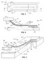
- FIG. 1is a plan view showing a spring structure according to a first embodiment of the present invention
- FIG. 2is a cross-sectional side view of the spring structure taken along section line 2 — 2 of FIG. 1, and the spring structure contacting a separate integrated circuit;
- FIG. 3is a cut-away perspective view of the spring structure shown in FIG. 1;
- FIGS. 4 (A) through 4 (J)are cross-sectional side views showing fabrication steps associated with the production of the spring structure shown in FIG. 1;
- FIGS. 5 (A) and 5 (B)are plan views showing the spring structure of FIG. 1 during selected fabrication steps;
- FIG. 6is a cut-away perspective view showing a spring structure according to a second embodiment of the present invention.
- FIG. 7is a plan view showing a release mask utilized to fabrication the spring structure shown in FIG. 6 .
- FIGS. 1, 2 and 3show a spring structure 100 according to a first embodiment of the present invention.
- FIG. 1is a plan view of spring structure 100
- FIG. 2is a cross-sectional side view taken along section line 2 — 2 of FIG. 1
- FIG. 3is a perspective view with a cut-away section indicated by section line 3 — 3 in FIG. 1 .
- Spring structure 100generally includes a substrate 101 , a release material portion 110 , and a spring metal finger 120 .
- Substrate 101e.g., glass
- Substrate 101includes an optional conductor 105 that can take several forms (i.e., a metal trace deposited on the substrate, as shown, or a buried conductor accessed by an opening in a passivation layer (not shown)). When present, conductor 105 may provide electrical connection between electronic components of an integrated circuit and spring structure 100 .
- conductor 105may be an exposed portion of conducting material that is electrically connected to redistribution traces, through substrate vias, solder bumps, solder balls, mounted electrical components, integrated passive components, or interconnect pads.
- Release material portion 110is formed on an upper surface of substrate 101 such that it contacts conductor 105 (if present).
- Spring metal finger 120includes an anchor portion 122 and a free (i.e., cantilevered) portion 125 .
- Anchor portion 122is attached to release material portion 110 (i.e., such that release material portion 110 is located between anchor portion 122 and substrate 101 ).
- Free portion 125which includes a tip 125 -T, extends from anchor portion 122 over substrate 101 , and includes an upper (first) surface 126 and an opposing lower (second) surface 127 that define a thickness T 1 in the range of 0.1 and 10 microns (see FIG. 2 ). Note that edges 128 of free portion 125 extend between upper surface 126 and lower surface 127 .
- spring metal finger 120is etched from a stress-engineered metal film that is formed by DC magnetron sputtering one or more metals using gas (e.g., Argon) pressure variations in the sputter environment during film growth in accordance with known techniques.
- gase.g., Argon
- sputtered metal filmscan be used to form tightly curved spring metal fingers, or very stiff spring metal fingers, but not both simultaneously because increasing the film thickness (which is necessary to increase stiffness) also increases the radius of the resulting spring metal finger.
- the internal stress of the stress-engineered metal filmcannot be increased arbitrarily because of material limitations.
- electrically conductive coating 130is formed to minimize contact resistance between spring metal finger 120 and contact structure (e.g., a contact pad 152 formed on a separate integrated circuit 150 , as shown in FIG. 2 ).
- conductive coating 130includes one or more of the refractory noble metals (e.g., Rhodium (Rh), Iridium (Ir), Rhenium (Re), Platinum (Pt), and Palladium (Pd)) having a thickness T 2 in the range of 0.1 and 3 microns (see FIG. 2 ).
- conductive coating 130is deposited on free portion 125 of spring metal finger 120 after free portion 125 is released (i.e., after release material located under free portion 125 is removed, thereby allowing internal stress to bend free portion 125 away from substrate 101 ). Because conductive coating 130 is formed after free portion 125 is released, conductive coating 130 is deposited on upper surface 126 and edges 128 of free portion 125 , and in particular on front edge 128 -T located at tip 128 . Accordingly, as shown in FIG. 2, spring structure 100 contacts external integrated circuit 150 through conductive coating 130 , thereby preventing increased contact resistance due to oxidation of spring metal finger 120 or galling of contact pad 152 .
- conductive coating 130 after releaseallows spring structure 100 to be relatively thick (and, therefore, stiff), thereby increasing the spring force constant of spring structure 100 at a lower cost than non-coated spring structures, or spring structures having conductive coating formed only on one side.
- the deposition processincreases a total thickness of free portion 125 by the thickness T 2 of conductive coating 130 .
- conductive coating 130is formed at very low cost because the basic two-mask process utilized for making non-coated spring structures is not violated (i.e., no additional masks are used to perform the coating deposition process).
- spring structure 100can be both tightly curved and relatively thick (and, therefore, stiff) at a lower cost than non-coated spring structures, or spring structures having conductive coating formed only on one side.
- the curvature R of free portion 125is partially determined by the thickness T 1 of the stress-engineered metal film from which it is etched.
- a relatively thin metal filmis required.
- spring structure 100can be both tightly curved and relatively thick by forming spring metal finger 120 from a thin stress-engineered metal film, and then forming a relatively thick of conductive coating 130 .
- conductive coating 130passivates spring metal finger 120 , which is important because most springy metals, such as stress-engineered metal film, form surface oxides. Conductive coating 130 also increases wear resistance and lubricity, and thereby resists the galling of an associated contact structure (e.g., contact pad 152 , which is shown in FIG. 2 ). Conductive coating 130 can also provide a compression stop to limit spring compression. Moreover, conductive coating 130 may be added to strengthen spring structure 100 by adding ductility. Finally, conductive coating 130 may be added to blunt the radii of process features and defects that can arise on spring metal finger 120 . The above-mentioned benefits are not intended to be exhaustive.
- optional conductor 105is included to provide electrical coupling of spring structure 100 to an external electrical system (not shown).
- the electrical coupling between spring metal finger 120 and conductor 105necessitates using an electrically conductive release material to form release material portion 110 .
- electrical couplingcan also be provided directly to spring metal finger 120 by other structures (e.g., wire bonding, or pre-patterning the release layer), thereby allowing the use of non-conducting release materials.
- the cost-to-thickness (stiffness) characteristics discussed abovemay also be beneficially exploited in applications in which spring metal finger 120 is not used to conduct electric signals.
- FIGS. 4 (A) through 4 (J) and FIGS. 5 (A) and 5 (B)illustrate a method for fabricating spring structure 100 (described above).
- release material layer 210is formed from an electrically conductive material, and a portion 210 A of release material layer 210 contacts a conductor 105 that is exposed on the upper surface of substrate 101 .
- release material layer 210is Titanium (Ti) that is sputter deposited onto substrate 101 to a thickness of approximately 0.2 microns or greater. Titanium provides desirable characteristics as a conductive release material layer due to its plasticity (i.e., its resistance to cracking) and its strong adhesion. Other release materials having the beneficial plastic characteristics of titanium may also be used.
- release material layer 210includes another metal, such as Copper (Cu), Aluminum (Al), Nickel (Ni), Zirconium (Zr), or Cobalt (Co). Release material layer 210 may also be formed using heavily doped silicon (Si). Further, two or more release material layers can be sequentially deposited to form a multi-layer structure. In yet another possible embodiment, any of the above-mentioned release materials can be sandwiched between two non-release material layers (i.e., materials that are not removed during the spring metal release process, described below). Alternatively, when it is not necessary to provide electrical conduction between the subsequently deposited spring metal layer and a contact pad (such as conductor 105 ), release material layer 210 can be a non-conducting material such as Silicon Nitride (SiN).
- SiNSilicon Nitride
- FIG. 4 (B)shows a stress-engineered metal film 220 formed on release material layer 210 using known processing techniques such that it includes internal stress variations in the growth direction.
- stress-engineered metal film 220is formed such that its lowermost portions (i.e., adjacent to release material layer 210 ) has a higher internal compressive stress than its upper portions, thereby causing stress-engineered metal film 220 to have internal stress variations that cause a spring metal finger to bend upward away from substrate 101 (discussed below).
- Methods for generating such internal stress variations in stress-engineered metal film 220are taught, for example, in U.S. Pat. No. 3,842,189 (depositing two metals having different internal stresses) and U.S. Pat. No.
- stress-engineered metal film 220includes Molybdenum and Chromium (MoCr) sputter deposited to a thickness of 1 micron.
- MoCrChromium
- a Mo spring metal layercan be formed on SiN release material layers.
- stress-engineered metal film 220is separated from conductor 105 by portion 210 A of release material layer 210 . Accordingly, a separate masking step utilized in conventional fabrication methods to form an opening in the release material is not required, thereby reducing fabrication costs. Instead, as discussed below, the present embodiment utilizes the conductivity of release material layer 210 to provide electrical connection between. conductor 105 and stress-engineered metal film 220 .
- elongated spring metal (first) masks 230are then patterned over a selected portion of stress-engineered metal film 220 . Note that each spring metal mask 230 extends over an associated conductor 105 (if present), as shown in FIG. 5 (A).
- exposed portions of stress-engineered metal film 220 surrounding the spring metal mask 230are etched using one or more etchants 240 to form a spring metal island 220 - 1 .
- this etching processis performed such that limited etching is performed in portions 210 B of release layer 210 that surround spring metal island 220 - 1 such that at least a partial thickness of release layer portion 210 B remains on substrate 101 after this etching step.
- the etching stepmay be performed using, for example, a wet etching process to remove exposed portions of stress-engineered metal film 220 . This embodiment was successfully performed using cerric ammonium nitrate solution to remove a MoCr spring metal layer.
- anisotropic dry etchingis used to etch both stress-engineered metal film 220 and the upper surface of release layer portion 210 B.
- This embodimentmay be performed, for example, with Mo spring metal, and Si or Ti release layers. Mo, Si and Ti all etch in reactive fluorine plasmas.
- An advantage of dry etching the spring metal filmis that it facilitates finer features and sharper tipped spring metal fingers. Materials that do not etch in reactive plasmas may still be etched anisotropically by physical ion etching methods, such as Argon ion milling.
- the etching stepcan be performed using the electrochemical etching process described in IBM J. Res. Dev. Vol. 42, No. 5, page 655 (Sep. 5, 1998), which is incorporated herein by reference. Many additional process variations and material substitutions are therefore possible and the examples given are not intended to be limiting.
- FIG. 4 (E)shows spring metal island 220 - 1 and release material 210 after spring metal mask 230 (FIG. 4 (D)) is removed. Note again that electrical connection between conductor 105 and spring metal island 220 - 1 is provided through portion 210 A of release material layer 210 .
- release (second) mask 250(e.g., photoresist) is then formed on a first portion 220 - 1 A of spring metal island 220 - 1 .
- Release mask 250defines a release window RW, which exposes a second portion 220 - 1 B of spring metal island 220 - 1 and surrounding portions 210 B of release material layer 210 .
- release mask 250is intentionally formed with a negative sloped side wall (for example, using negative resist or image reversal techniques) to facilitate the liftoff of the conductive coating deposited thereon, as discussed below.
- release mask 250is formed such that each spring metal island 230 ( 1 ) through 230 ( 3 ) formed on substrate 101 is exposed through a separate release window RW 1 through RW 3 , respectively.
- Separate release windowsare provided for each spring structure because the release window will also define the pattern of the subsequently deposited conductive coating. That is, if two or more spring structures were exposed through the same window, then conductive coating would be deposited on substrate 101 separating the two spring structures, which would require an additional etching mask to remove the residual coating. Accordingly, by providing separate release windows for each spring structure, the total number of required masks is minimized. Note, however, that separate release windows result in greater spacing between spring structures to facilitate the formation of the release mask wall separating the release windows. That is, providing space for these release mask walls implies in principle that the spring structures need to be further apart.
- FIG. 5 (B)also indicates an optional dice line DL that extend along the resist mask walls located between spring metal island 230 ( 3 ) and an adjacent group of spring structures (not shown).
- substrate 101is diced between the formation of release window 250 and the lifting of the springs (discussed below).
- batch processing spring structuresis facilitated in that all of the masking is done before dicing (i.e., because no further masks are required to deposit and/or etch the conductive coating), thereby permitting a substantial reduction in total production costs in comparison to production processes, for example, in which the lifted and coated spring metal fingers are dipped into a masking material.
- a release etchant 260e.g., a buffered oxide etch
- a release etchant 260is then use to selectively remove a portion of the release material layer from beneath the exposed portion of the spring metal island to form spring metal finger 120 (discussed above with reference to FIGS. 1 - 3 ).
- removal of the exposed release materialcauses free portion 125 to bend away from substrate 101 due to the internal stress variations established during the formation of the spring metal film (discussed above).
- anchor portion 122remains secured to substrate 101 by release material portion 110 , which is protected by release mask 250 .
- release material portion 110is formed from a conductive release material, the resulting spring structure is electrically coupled to conductor 105 .
- FIG. 4 (H)depicts an optional step for in-situ milling or back sputtering 270 that prepares the metal surfaces of free portion 125 for optimal adherence of the subsequently applied coating using known techniques.
- FIG. 4 (I)shows the deposition of conductive coating 130 on free portion 125 after release.
- this deposition stepis performed using a directional deposition source (e.g., using line-of-sight material flux from a small area source, such as electron beam evaporation or sputter deposition using a material collimator). Note that by performing the deposition of conductive coating 130 after free portion 125 is lifted, top surface 126 and front edge 128 -T located at tip 125 -T of free portion 125 face into the deposition to facilitate uniform coating.
- a directional deposition sourcee.g., using line-of-sight material flux from a small area source, such as electron beam evaporation or sputter deposition using a material collimator.
- the directional depositionfacilitates the formation of conductive coating 130 on front edge 128 -T of free portion 125 after it is lifted, better coverage of tip 125 -T is achieved than if deposition is performed before release. Further, deposition of conductive coating 130 before the release process runs the risk that the deposited coating will overlay the release layer, and prevent or impede the flow of release etchant 260 under free portion 125 (see FIG. 4 (G) for reference) of the spring structure.
- FIG. 4 (I)also shows the deposition of residual coating portions 130 -R 1 on release mask 250 , and the deposition of residual coating portions 130 -R 2 on regions of substrate 101 that are exposed through the release window (i.e., adjacent to released free portion 125 ).
- residual coating portions 130 -R 2which are not removed by subsequent removal of release mask 250 , are not deposited on portions 101 -S of substrate 101 that are shadowed by spring metal finger 125 .
- the negative-sloped side wall of release mask 250produces an exposed edge 250 -E between coating portion 130 and residual coating portion 130 -R 1 that allows access of a solvent during release mask etch (discussed below) to facilitate liftoff of residual coating portion 130 -R 1 .
- FIG. 4 (J)shows spring structure 100 during the removal of release mask 250 and residual coating portions 130 -R 1 (see FIG. 4 (I)).
- the negative-sloped side wall of release mask 250produces an exposed edge 250 -E between coating portion 130 and residual coating portion 130 -R 1 .
- this exposed edgeallows access of a solvent 270 that dissolves release mask using known techniques. For example, when the release mask is image-reversed photoresist, acetone can be used as solvent 270 . As the release mask is dissolved, residual coating portions formed thereon are lifted off. If necessary, agitation may be used to accelerate the lift-off process.
- FIG. 6shows a spring structure 300 according to a second embodiment of the present invention. Similar to spring structure 100 (discussed above), spring structure 300 includes a release layer portion 110 formed on a conductor 105 , a spring metal finger 120 formed on release layer portion 110 , and a conductive coating 330 formed on spring metal finger 120 . However, spring structure 300 differs from spring structure 100 in that conductive coating 330 is formed on both free portion 125 and anchored portion 122 of spring metal finger 120 (referring to FIG. 3, conductive coating 130 only covers free portion 125 ). Specifically, conductive coating 330 is formed on both sides of free portion 125 , as described above, and is also formed on an upper surface of anchored portion 122 .
- resilient springy metalssuch as MoCr exhibit relatively high resistance in comparison to many forms of conductive coating, such as Ni, Au and Cu. Accordingly, by extending conductive coating 330 over anchored portion 122 , currents passing between free portion 125 and conductor 105 are subjected to less resistance than in spring structure 100 due to the presence of conductive coating 330 on anchor portion 122 .
- FIG. 7is a plan view showing a release mask 450 utilized in the fabrication of spring structure 300 (FIG. 6 ).
- Release mask 450is similar to release mask 250 (shown in FIG. 5 (B)), except that the release window defined by release mask 450 exposes part of the anchored portion of each spring metal island 220 ( 1 ) through 220 ( 3 ).
- release window 450includes a channel 455 that extends over anchored portion 222 .
- channel 455overlaps the outer edge 229 of anchor portion 222 by an overlap width OL of 1 to 10 microns to prevent unintended release of anchor portion 222 .
- this overlapproduces a step structure shoulder 325 extending along the edge of anchor portion 122 after release, deposition, and removal of the release mask.
Landscapes
- Engineering & Computer Science (AREA)
- Manufacturing & Machinery (AREA)
- Microelectronics & Electronic Packaging (AREA)
- Physics & Mathematics (AREA)
- General Physics & Mathematics (AREA)
- Mechanical Engineering (AREA)
- Measuring Leads Or Probes (AREA)
- Chemical Vapour Deposition (AREA)
- Springs (AREA)
Abstract
Description
Claims (12)
Priority Applications (5)
| Application Number | Priority Date | Filing Date | Title |
|---|---|---|---|
| US09/904,370US6560861B2 (en) | 2001-07-11 | 2001-07-11 | Microspring with conductive coating deposited on tip after release |
| EP02254667AEP1277696B1 (en) | 2001-07-11 | 2002-07-03 | Spring with conductive coating |
| DE60212906TDE60212906T2 (en) | 2001-07-11 | 2002-07-03 | Spring with conductive coating |
| JP2002195437AJP2003097617A (en) | 2001-07-11 | 2002-07-04 | Micro spring forming conductor covering on tip portion after releasing |
| US10/323,382US20030096519A1 (en) | 2001-07-11 | 2002-12-17 | Microspring with conductive coating deposited on tip after release |
Applications Claiming Priority (1)
| Application Number | Priority Date | Filing Date | Title |
|---|---|---|---|
| US09/904,370US6560861B2 (en) | 2001-07-11 | 2001-07-11 | Microspring with conductive coating deposited on tip after release |
Related Child Applications (1)
| Application Number | Title | Priority Date | Filing Date |
|---|---|---|---|
| US10/323,382DivisionUS20030096519A1 (en) | 2001-07-11 | 2002-12-17 | Microspring with conductive coating deposited on tip after release |
Publications (2)
| Publication Number | Publication Date |
|---|---|
| US20030010615A1 US20030010615A1 (en) | 2003-01-16 |
| US6560861B2true US6560861B2 (en) | 2003-05-13 |
Family
ID=25419030
Family Applications (2)
| Application Number | Title | Priority Date | Filing Date |
|---|---|---|---|
| US09/904,370Expired - LifetimeUS6560861B2 (en) | 2001-07-11 | 2001-07-11 | Microspring with conductive coating deposited on tip after release |
| US10/323,382AbandonedUS20030096519A1 (en) | 2001-07-11 | 2002-12-17 | Microspring with conductive coating deposited on tip after release |
Family Applications After (1)
| Application Number | Title | Priority Date | Filing Date |
|---|---|---|---|
| US10/323,382AbandonedUS20030096519A1 (en) | 2001-07-11 | 2002-12-17 | Microspring with conductive coating deposited on tip after release |
Country Status (4)
| Country | Link |
|---|---|
| US (2) | US6560861B2 (en) |
| EP (1) | EP1277696B1 (en) |
| JP (1) | JP2003097617A (en) |
| DE (1) | DE60212906T2 (en) |
Cited By (32)
| Publication number | Priority date | Publication date | Assignee | Title |
|---|---|---|---|---|
| US20030071330A1 (en)* | 2001-10-12 | 2003-04-17 | Romano Linda T. | Spring structure with strees-balancing layer |
| US20030211761A1 (en)* | 2001-02-09 | 2003-11-13 | Xerox Corporation | Low cost integrated out-of-plane micro-device structures and method of making |
| US20050070131A1 (en)* | 2003-09-29 | 2005-03-31 | Cookson Electronics, Inc. | Electrical circuit assembly with micro-socket |
| US20060053625A1 (en)* | 2002-05-07 | 2006-03-16 | Microfabrica Inc. | Microprobe tips and methods for making |
| US20060068612A1 (en)* | 2003-11-03 | 2006-03-30 | January Kister | Multipath interconnect with meandering contact cantilevers |
| US20060180927A1 (en)* | 2005-02-14 | 2006-08-17 | Daisuke Takai | Contact structure and method for manufacturing the same |
| US20070125486A1 (en)* | 2005-12-02 | 2007-06-07 | Palo Alto Research Center Incorporated | Vertically spaced plural microsprings |
| US20080108221A1 (en)* | 2003-12-31 | 2008-05-08 | Microfabrica Inc. | Microprobe Tips and Methods for Making |
| US20080211524A1 (en)* | 2003-02-04 | 2008-09-04 | Microfabrica Inc. | Electrochemically Fabricated Microprobes |
| CN100439234C (en)* | 2005-12-29 | 2008-12-03 | 中国科学院上海微系统与信息技术研究所 | Manufacturing method of anchor in xenon difluoride gas corrosion process |
| US20090140433A1 (en)* | 2007-11-30 | 2009-06-04 | Alces Technology, Inc. | MEMS chip-to-chip interconnects |
| US20090159996A1 (en)* | 2007-12-21 | 2009-06-25 | Palo Alto Research Center Incorporated | Method Of Producing Microsprings Having Nanowire Tip Structures |
| US20090256583A1 (en)* | 2003-02-04 | 2009-10-15 | Microfabrica Inc. | Vertical Microprobes for Contacting Electronic Components and Method for Making Such Probes |
| US20100155253A1 (en)* | 2002-05-07 | 2010-06-24 | Microfabrica Inc. | Microprobe Tips and Methods for Making |
| US20110198745A1 (en)* | 2010-02-17 | 2011-08-18 | Maxim Integrated Products, Inc. | Wafer-level packaged device having self-assembled resilient leads |
| US8441808B2 (en) | 2010-09-22 | 2013-05-14 | Palo Alto Research Center Incorporated | Interposer with microspring contacts |
| US8519534B2 (en) | 2010-09-22 | 2013-08-27 | Palo Alto Research Center Incorporated | Microsprings partially embedded in a laminate structure and methods for producing same |
| US8525353B2 (en) | 2011-12-19 | 2013-09-03 | Palo Alto Research Center Incorporated | Microspring structures adapted for target device cooling |
| US8686560B2 (en) | 2010-04-07 | 2014-04-01 | Maxim Integrated Products, Inc. | Wafer-level chip-scale package device having bump assemblies configured to mitigate failures due to stress |
| US8717055B2 (en) | 2003-02-04 | 2014-05-06 | Microfabrica Inc. | Probe devices formed from multiple planar layers of structural material with tip regions formed from one or more intermediate planar layers |
| US10416192B2 (en) | 2003-02-04 | 2019-09-17 | Microfabrica Inc. | Cantilever microprobes for contacting electronic components |
| US11262383B1 (en) | 2018-09-26 | 2022-03-01 | Microfabrica Inc. | Probes having improved mechanical and/or electrical properties for making contact between electronic circuit elements and methods for making |
| US11761982B1 (en) | 2019-12-31 | 2023-09-19 | Microfabrica Inc. | Probes with planar unbiased spring elements for electronic component contact and methods for making such probes |
| US11774467B1 (en) | 2020-09-01 | 2023-10-03 | Microfabrica Inc. | Method of in situ modulation of structural material properties and/or template shape |
| US11802891B1 (en) | 2019-12-31 | 2023-10-31 | Microfabrica Inc. | Compliant pin probes with multiple spring segments and compression spring deflection stabilization structures, methods for making, and methods for using |
| US11973301B2 (en) | 2018-09-26 | 2024-04-30 | Microfabrica Inc. | Probes having improved mechanical and/or electrical properties for making contact between electronic circuit elements and methods for making |
| US12000865B2 (en) | 2019-02-14 | 2024-06-04 | Microfabrica Inc. | Multi-beam vertical probes with independent arms formed of a high conductivity metal for enhancing current carrying capacity and methods for making such probes |
| US12078657B2 (en) | 2019-12-31 | 2024-09-03 | Microfabrica Inc. | Compliant pin probes with extension springs, methods for making, and methods for using |
| US12146898B2 (en) | 2020-10-02 | 2024-11-19 | Microfabrica Inc. | Multi-beam probes with decoupled structural and current carrying beams and methods of making |
| US12181493B2 (en) | 2018-10-26 | 2024-12-31 | Microfabrica Inc. | Compliant probes including dual independently operable probe contact elements including at least one flat extension spring, methods for making, and methods for using |
| US12196781B2 (en) | 2019-12-31 | 2025-01-14 | Microfabrica Inc. | Probes with planar unbiased spring elements for electronic component contact, methods for making such probes, and methods for using such probes |
| US12196782B2 (en) | 2019-12-31 | 2025-01-14 | Microfabrica Inc. | Probes with planar unbiased spring elements for electronic component contact, methods for making such probes, and methods for using such probes |
Families Citing this family (31)
| Publication number | Priority date | Publication date | Assignee | Title |
|---|---|---|---|---|
| US6812718B1 (en)* | 1999-05-27 | 2004-11-02 | Nanonexus, Inc. | Massively parallel interface for electronic circuits |
| US7382142B2 (en) | 2000-05-23 | 2008-06-03 | Nanonexus, Inc. | High density interconnect system having rapid fabrication cycle |
| US6799976B1 (en)* | 1999-07-28 | 2004-10-05 | Nanonexus, Inc. | Construction structures and manufacturing processes for integrated circuit wafer probe card assemblies |
| US7247035B2 (en)* | 2000-06-20 | 2007-07-24 | Nanonexus, Inc. | Enhanced stress metal spring contactor |
| US7349223B2 (en) | 2000-05-23 | 2008-03-25 | Nanonexus, Inc. | Enhanced compliant probe card systems having improved planarity |
| US20070245553A1 (en)* | 1999-05-27 | 2007-10-25 | Chong Fu C | Fine pitch microfabricated spring contact structure & method |
| US7952373B2 (en)* | 2000-05-23 | 2011-05-31 | Verigy (Singapore) Pte. Ltd. | Construction structures and manufacturing processes for integrated circuit wafer probe card assemblies |
| US7579848B2 (en)* | 2000-05-23 | 2009-08-25 | Nanonexus, Inc. | High density interconnect system for IC packages and interconnect assemblies |
| WO2003018865A1 (en)* | 2001-08-24 | 2003-03-06 | Nanonexus, Inc. | Method and apparatus for producing uniform isotropic stresses in a sputtered film |
| US8914590B2 (en)* | 2002-08-07 | 2014-12-16 | Pact Xpp Technologies Ag | Data processing method and device |
| US6866255B2 (en)* | 2002-04-12 | 2005-03-15 | Xerox Corporation | Sputtered spring films with low stress anisotropy |
| US7015584B2 (en)* | 2003-07-08 | 2006-03-21 | Xerox Corporation | High force metal plated spring structure |
| US7410590B2 (en)* | 2003-12-19 | 2008-08-12 | Palo Alto Research Center Incorporated | Transferable micro spring structure |
| JP4747562B2 (en)* | 2004-06-25 | 2011-08-17 | 株式会社日立製作所 | Rare earth magnet, manufacturing method thereof, and magnet motor |
| JP4382593B2 (en)* | 2004-06-29 | 2009-12-16 | 山一電機株式会社 | Probe unit and manufacturing method thereof |
| US7082684B2 (en)* | 2004-08-04 | 2006-08-01 | Palo Alto Research Center Incorporated | Intermetallic spring structure |
| US20060030179A1 (en)* | 2004-08-05 | 2006-02-09 | Palo Alto Research Center, Incorporated | Transmission-line spring structure |
| US7230440B2 (en) | 2004-10-21 | 2007-06-12 | Palo Alto Research Center Incorporated | Curved spring structure with elongated section located under cantilevered section |
| US8330485B2 (en)* | 2004-10-21 | 2012-12-11 | Palo Alto Research Center Incorporated | Curved spring structure with downturned tip |
| JP2007165383A (en) | 2005-12-09 | 2007-06-28 | Ibiden Co Ltd | Printed wiring board having component mounting pin formed thereon |
| JP4654897B2 (en) | 2005-12-09 | 2011-03-23 | イビデン株式会社 | Method for manufacturing printed wiring board having component mounting pins |
| JP4848752B2 (en)* | 2005-12-09 | 2011-12-28 | イビデン株式会社 | Printed wiring board having component mounting pins and electronic device using the same |
| US7982290B2 (en)* | 2006-01-12 | 2011-07-19 | Palo Alto Research Center, Inc. | Contact spring application to semiconductor devices |
| TWI332086B (en)* | 2006-10-24 | 2010-10-21 | Ind Tech Res Inst | Multi-layer electric probe and fabricating method |
| DE202008001997U1 (en)* | 2008-02-14 | 2008-04-03 | Rosenberger Hochfrequenztechnik Gmbh & Co. Kg | contact spring |
| US8643140B2 (en)* | 2011-07-11 | 2014-02-04 | United Microelectronics Corp. | Suspended beam for use in MEMS device |
| JP6379416B2 (en)* | 2014-10-31 | 2018-08-29 | 北川工業株式会社 | Contact member |
| DE102015211472A1 (en)* | 2015-06-22 | 2016-07-07 | Carl Zeiss Smt Gmbh | MICRO-ELECTROMECHANICAL SYSTEM AND METHOD FOR MANUFACTURING A MICRO-ELECTROMECHANICAL SYSTEM |
| US11201275B1 (en)* | 2020-06-10 | 2021-12-14 | Palo Alto Research Center Incorporated | Superconducting stress-engineered micro-fabricated springs |
| US11908782B2 (en)* | 2021-03-22 | 2024-02-20 | Xerox Corporation | Spacers formed on a substrate with etched micro-springs |
| US12224082B2 (en)* | 2023-02-09 | 2025-02-11 | Xerox Corporation | Stress engineered microspring for cryogenic superconducting circuits |
Citations (3)
| Publication number | Priority date | Publication date | Assignee | Title |
|---|---|---|---|---|
| US3842189A (en) | 1973-01-08 | 1974-10-15 | Rca Corp | Contact array and method of making the same |
| US5613861A (en) | 1995-06-07 | 1997-03-25 | Xerox Corporation | Photolithographically patterned spring contact |
| US6117694A (en)* | 1994-07-07 | 2000-09-12 | Tessera, Inc. | Flexible lead structures and methods of making same |
Family Cites Families (8)
| Publication number | Priority date | Publication date | Assignee | Title |
|---|---|---|---|---|
| US5917707A (en)* | 1993-11-16 | 1999-06-29 | Formfactor, Inc. | Flexible contact structure with an electrically conductive shell |
| EP0839321B1 (en)* | 1996-05-17 | 2006-01-11 | FormFactor, Inc. | Contact tip structures for microelectronic interconnection elements and methods of making same |
| JPH11504725A (en)* | 1996-05-17 | 1999-04-27 | フォームファクター,インコーポレイテッド | Microelectronic spring contact parts |
| DE19736674C1 (en)* | 1997-08-22 | 1998-11-26 | Siemens Ag | Micromechanical electrostatic relay |
| EP1135690B1 (en)* | 1998-12-02 | 2003-06-04 | Formfactor, Inc. | Lithographic contact elements |
| US6366414B1 (en)* | 1999-09-03 | 2002-04-02 | Agere Systems Guardian Corp. | Micro-electro-mechanical optical device |
| US6794725B2 (en)* | 1999-12-21 | 2004-09-21 | Xerox Corporation | Amorphous silicon sensor with micro-spring interconnects for achieving high uniformity in integrated light-emitting sources |
| US6827584B2 (en)* | 1999-12-28 | 2004-12-07 | Formfactor, Inc. | Interconnect for microelectronic structures with enhanced spring characteristics |
- 2001
- 2001-07-11USUS09/904,370patent/US6560861B2/ennot_activeExpired - Lifetime
- 2002
- 2002-07-03EPEP02254667Apatent/EP1277696B1/ennot_activeExpired - Lifetime
- 2002-07-03DEDE60212906Tpatent/DE60212906T2/ennot_activeExpired - Lifetime
- 2002-07-04JPJP2002195437Apatent/JP2003097617A/enactivePending
- 2002-12-17USUS10/323,382patent/US20030096519A1/ennot_activeAbandoned
Patent Citations (5)
| Publication number | Priority date | Publication date | Assignee | Title |
|---|---|---|---|---|
| US3842189A (en) | 1973-01-08 | 1974-10-15 | Rca Corp | Contact array and method of making the same |
| US6117694A (en)* | 1994-07-07 | 2000-09-12 | Tessera, Inc. | Flexible lead structures and methods of making same |
| US5613861A (en) | 1995-06-07 | 1997-03-25 | Xerox Corporation | Photolithographically patterned spring contact |
| US6184699B1 (en)* | 1995-06-07 | 2001-02-06 | Xerox Corporation | Photolithographically patterned spring contact |
| US6264477B1 (en)* | 1995-06-07 | 2001-07-24 | Xerox Corporation | Photolithographically patterned spring contact |
Cited By (52)
| Publication number | Priority date | Publication date | Assignee | Title |
|---|---|---|---|---|
| US20030211761A1 (en)* | 2001-02-09 | 2003-11-13 | Xerox Corporation | Low cost integrated out-of-plane micro-device structures and method of making |
| US6848175B2 (en)* | 2001-02-09 | 2005-02-01 | Xerox Corporation | Method of forming an out-of-plane structure |
| US6794737B2 (en)* | 2001-10-12 | 2004-09-21 | Xerox Corporation | Spring structure with stress-balancing layer |
| US20030071330A1 (en)* | 2001-10-12 | 2003-04-17 | Romano Linda T. | Spring structure with strees-balancing layer |
| US20060053625A1 (en)* | 2002-05-07 | 2006-03-16 | Microfabrica Inc. | Microprobe tips and methods for making |
| US20100155253A1 (en)* | 2002-05-07 | 2010-06-24 | Microfabrica Inc. | Microprobe Tips and Methods for Making |
| US10788512B2 (en) | 2003-02-04 | 2020-09-29 | Microfabrica Inc. | Cantilever microprobes for contacting electronic components |
| US8729916B2 (en) | 2003-02-04 | 2014-05-20 | Microfabrica Inc. | Methods of creating probe structures from a plurality of planar layers |
| US10416192B2 (en) | 2003-02-04 | 2019-09-17 | Microfabrica Inc. | Cantilever microprobes for contacting electronic components |
| US8717055B2 (en) | 2003-02-04 | 2014-05-06 | Microfabrica Inc. | Probe devices formed from multiple planar layers of structural material with tip regions formed from one or more intermediate planar layers |
| US8717054B2 (en) | 2003-02-04 | 2014-05-06 | Microfabrica Inc. | Methods of creating probe structures from a plurality of planar layers |
| US20080211524A1 (en)* | 2003-02-04 | 2008-09-04 | Microfabrica Inc. | Electrochemically Fabricated Microprobes |
| US8723543B2 (en) | 2003-02-04 | 2014-05-13 | Microfabrica Inc. | Methods of creating probe structures from a plurality of planar layers |
| US20100134131A1 (en)* | 2003-02-04 | 2010-06-03 | Microfabrica Inc. | Electrochemically Fabricated Microprobes |
| US20090256583A1 (en)* | 2003-02-04 | 2009-10-15 | Microfabrica Inc. | Vertical Microprobes for Contacting Electronic Components and Method for Making Such Probes |
| US20050070131A1 (en)* | 2003-09-29 | 2005-03-31 | Cookson Electronics, Inc. | Electrical circuit assembly with micro-socket |
| US6881074B1 (en) | 2003-09-29 | 2005-04-19 | Cookson Electronics, Inc. | Electrical circuit assembly with micro-socket |
| US20060068612A1 (en)* | 2003-11-03 | 2006-03-30 | January Kister | Multipath interconnect with meandering contact cantilevers |
| US20080108221A1 (en)* | 2003-12-31 | 2008-05-08 | Microfabrica Inc. | Microprobe Tips and Methods for Making |
| US20060180927A1 (en)* | 2005-02-14 | 2006-08-17 | Daisuke Takai | Contact structure and method for manufacturing the same |
| US7550855B2 (en) | 2005-12-02 | 2009-06-23 | Palo Alto Research Center Incorporated | Vertically spaced plural microsprings |
| US20070125486A1 (en)* | 2005-12-02 | 2007-06-07 | Palo Alto Research Center Incorporated | Vertically spaced plural microsprings |
| CN100439234C (en)* | 2005-12-29 | 2008-12-03 | 中国科学院上海微系统与信息技术研究所 | Manufacturing method of anchor in xenon difluoride gas corrosion process |
| US20090140433A1 (en)* | 2007-11-30 | 2009-06-04 | Alces Technology, Inc. | MEMS chip-to-chip interconnects |
| US20110163061A1 (en)* | 2007-12-21 | 2011-07-07 | Palo Alto Research Center Incorporated | Method Of Producing Microsprings Having Nanowire Tip Structures |
| US20110167526A1 (en)* | 2007-12-21 | 2011-07-07 | Palo Alto Research Center Incorporated | Microsprings Having Nanowire Tip Structures |
| US7927905B2 (en)* | 2007-12-21 | 2011-04-19 | Palo Alto Research Center Incorporated | Method of producing microsprings having nanowire tip structures |
| US20090159996A1 (en)* | 2007-12-21 | 2009-06-25 | Palo Alto Research Center Incorporated | Method Of Producing Microsprings Having Nanowire Tip Structures |
| US9159684B1 (en) | 2010-02-17 | 2015-10-13 | Maxim Integrated Products, Inc. | Wafer-level packaged device having self-assembled resilient leads |
| US8278748B2 (en)* | 2010-02-17 | 2012-10-02 | Maxim Integrated Products, Inc. | Wafer-level packaged device having self-assembled resilient leads |
| US20110198745A1 (en)* | 2010-02-17 | 2011-08-18 | Maxim Integrated Products, Inc. | Wafer-level packaged device having self-assembled resilient leads |
| US8692367B1 (en)* | 2010-02-17 | 2014-04-08 | Maxim Integrated Products, Inc. | Wafer-level packaged device having self-assembled resilient leads |
| US8686560B2 (en) | 2010-04-07 | 2014-04-01 | Maxim Integrated Products, Inc. | Wafer-level chip-scale package device having bump assemblies configured to mitigate failures due to stress |
| US8519534B2 (en) | 2010-09-22 | 2013-08-27 | Palo Alto Research Center Incorporated | Microsprings partially embedded in a laminate structure and methods for producing same |
| US9967982B2 (en) | 2010-09-22 | 2018-05-08 | Palo Alto Research Center Incorporated | Method of producing an interposer with microspring contacts |
| US8441808B2 (en) | 2010-09-22 | 2013-05-14 | Palo Alto Research Center Incorporated | Interposer with microspring contacts |
| US8525353B2 (en) | 2011-12-19 | 2013-09-03 | Palo Alto Research Center Incorporated | Microspring structures adapted for target device cooling |
| US11262383B1 (en) | 2018-09-26 | 2022-03-01 | Microfabrica Inc. | Probes having improved mechanical and/or electrical properties for making contact between electronic circuit elements and methods for making |
| US11982689B2 (en) | 2018-09-26 | 2024-05-14 | Microfabrica Inc. | Probes having improved mechanical and/or electrical properties for making contact between electronic circuit elements and methods for making |
| US11973301B2 (en) | 2018-09-26 | 2024-04-30 | Microfabrica Inc. | Probes having improved mechanical and/or electrical properties for making contact between electronic circuit elements and methods for making |
| US12181493B2 (en) | 2018-10-26 | 2024-12-31 | Microfabrica Inc. | Compliant probes including dual independently operable probe contact elements including at least one flat extension spring, methods for making, and methods for using |
| US12000865B2 (en) | 2019-02-14 | 2024-06-04 | Microfabrica Inc. | Multi-beam vertical probes with independent arms formed of a high conductivity metal for enhancing current carrying capacity and methods for making such probes |
| US11906549B1 (en) | 2019-12-31 | 2024-02-20 | Microfabrica Inc. | Compliant pin probes with flat extension springs, methods for making, and methods for using |
| US11867721B1 (en) | 2019-12-31 | 2024-01-09 | Microfabrica Inc. | Probes with multiple springs, methods for making, and methods for using |
| US11802891B1 (en) | 2019-12-31 | 2023-10-31 | Microfabrica Inc. | Compliant pin probes with multiple spring segments and compression spring deflection stabilization structures, methods for making, and methods for using |
| US12066462B2 (en) | 2019-12-31 | 2024-08-20 | Microfabrica Inc. | Probes with planar unbiased spring elements for electronic component contact and methods for making such probes |
| US12078657B2 (en) | 2019-12-31 | 2024-09-03 | Microfabrica Inc. | Compliant pin probes with extension springs, methods for making, and methods for using |
| US11761982B1 (en) | 2019-12-31 | 2023-09-19 | Microfabrica Inc. | Probes with planar unbiased spring elements for electronic component contact and methods for making such probes |
| US12196781B2 (en) | 2019-12-31 | 2025-01-14 | Microfabrica Inc. | Probes with planar unbiased spring elements for electronic component contact, methods for making such probes, and methods for using such probes |
| US12196782B2 (en) | 2019-12-31 | 2025-01-14 | Microfabrica Inc. | Probes with planar unbiased spring elements for electronic component contact, methods for making such probes, and methods for using such probes |
| US11774467B1 (en) | 2020-09-01 | 2023-10-03 | Microfabrica Inc. | Method of in situ modulation of structural material properties and/or template shape |
| US12146898B2 (en) | 2020-10-02 | 2024-11-19 | Microfabrica Inc. | Multi-beam probes with decoupled structural and current carrying beams and methods of making |
Also Published As
| Publication number | Publication date |
|---|---|
| DE60212906D1 (en) | 2006-08-17 |
| JP2003097617A (en) | 2003-04-03 |
| EP1277696A3 (en) | 2004-04-07 |
| US20030096519A1 (en) | 2003-05-22 |
| EP1277696A2 (en) | 2003-01-22 |
| US20030010615A1 (en) | 2003-01-16 |
| DE60212906T2 (en) | 2007-01-18 |
| EP1277696B1 (en) | 2006-07-05 |
Similar Documents
| Publication | Publication Date | Title |
|---|---|---|
| US6560861B2 (en) | Microspring with conductive coating deposited on tip after release | |
| US6684499B2 (en) | Method for fabricating a spring structure | |
| US6528350B2 (en) | Method for fabricating a metal plated spring structure | |
| US6658728B2 (en) | Method for fabricating a spring structure on a substrate | |
| US6713374B2 (en) | Interconnect assemblies and methods | |
| US8435612B2 (en) | Micro-machined structure production using encapsulation | |
| US7293996B2 (en) | Transmission-line spring structure | |
| US6651325B2 (en) | Method for forming cantilever beam probe card and probe card formed | |
| US6400166B2 (en) | Micro probe and method of fabricating same | |
| US20090035959A1 (en) | Interconnect assemblies and methods | |
| WO2001048870A2 (en) | Interconnect for microelectronic structures with enhanced spring characteristics | |
| US6794737B2 (en) | Spring structure with stress-balancing layer | |
| US20050006829A1 (en) | High force metal plated spring structure | |
| KR100807426B1 (en) | Interconnect Assemblies and Methods |
Legal Events
| Date | Code | Title | Description |
|---|---|---|---|
| AS | Assignment | Owner name:XEROX CORPORATION, CONNECTICUT Free format text:ASSIGNMENT OF ASSIGNORS INTEREST;ASSIGNORS:FORK, DAVID K.;CHUA, CHRISTOPHER L.;REEL/FRAME:012005/0023 Effective date:20010709 | |
| AS | Assignment | Owner name:BANK ONE, NA, AS ADMINISTRATIVE AGENT, ILLINOIS Free format text:SECURITY AGREEMENT;ASSIGNOR:XEROX CORPORATION;REEL/FRAME:013111/0001 Effective date:20020621 Owner name:BANK ONE, NA, AS ADMINISTRATIVE AGENT,ILLINOIS Free format text:SECURITY AGREEMENT;ASSIGNOR:XEROX CORPORATION;REEL/FRAME:013111/0001 Effective date:20020621 | |
| STCF | Information on status: patent grant | Free format text:PATENTED CASE | |
| AS | Assignment | Owner name:JPMORGAN CHASE BANK, AS COLLATERAL AGENT, TEXAS Free format text:SECURITY AGREEMENT;ASSIGNOR:XEROX CORPORATION;REEL/FRAME:015134/0476 Effective date:20030625 Owner name:JPMORGAN CHASE BANK, AS COLLATERAL AGENT,TEXAS Free format text:SECURITY AGREEMENT;ASSIGNOR:XEROX CORPORATION;REEL/FRAME:015134/0476 Effective date:20030625 | |
| FPAY | Fee payment | Year of fee payment:4 | |
| CC | Certificate of correction | ||
| FPAY | Fee payment | Year of fee payment:8 | |
| FPAY | Fee payment | Year of fee payment:12 | |
| AS | Assignment | Owner name:XEROX CORPORATION, CONNECTICUT Free format text:RELEASE BY SECURED PARTY;ASSIGNOR:JPMORGAN CHASE BANK, N.A. AS SUCCESSOR-IN-INTEREST ADMINISTRATIVE AGENT AND COLLATERAL AGENT TO BANK ONE, N.A.;REEL/FRAME:061388/0388 Effective date:20220822 Owner name:XEROX CORPORATION, CONNECTICUT Free format text:RELEASE BY SECURED PARTY;ASSIGNOR:JPMORGAN CHASE BANK, N.A. AS SUCCESSOR-IN-INTEREST ADMINISTRATIVE AGENT AND COLLATERAL AGENT TO JPMORGAN CHASE BANK;REEL/FRAME:066728/0193 Effective date:20220822 |