US6560680B2 - System controller with Integrated low latency memory using non-cacheable memory physically distinct from main memory - Google Patents
System controller with Integrated low latency memory using non-cacheable memory physically distinct from main memoryDownload PDFInfo
- Publication number
- US6560680B2 US6560680B2US09/994,302US99430201AUS6560680B2US 6560680 B2US6560680 B2US 6560680B2US 99430201 AUS99430201 AUS 99430201AUS 6560680 B2US6560680 B2US 6560680B2
- Authority
- US
- United States
- Prior art keywords
- memory
- low latency
- subset
- computer system
- address space
- Prior art date
- Legal status (The legal status is an assumption and is not a legal conclusion. Google has not performed a legal analysis and makes no representation as to the accuracy of the status listed.)
- Expired - Lifetime
Links
Images


Classifications
- G—PHYSICS
- G06—COMPUTING OR CALCULATING; COUNTING
- G06F—ELECTRIC DIGITAL DATA PROCESSING
- G06F12/00—Accessing, addressing or allocating within memory systems or architectures
- G06F12/02—Addressing or allocation; Relocation
- G06F12/08—Addressing or allocation; Relocation in hierarchically structured memory systems, e.g. virtual memory systems
- G06F12/0802—Addressing of a memory level in which the access to the desired data or data block requires associative addressing means, e.g. caches
- G06F12/0806—Multiuser, multiprocessor or multiprocessing cache systems
- G06F12/0815—Cache consistency protocols
- G06F12/0831—Cache consistency protocols using a bus scheme, e.g. with bus monitoring or watching means
- G06F12/0835—Cache consistency protocols using a bus scheme, e.g. with bus monitoring or watching means for main memory peripheral accesses (e.g. I/O or DMA)
- G—PHYSICS
- G06—COMPUTING OR CALCULATING; COUNTING
- G06F—ELECTRIC DIGITAL DATA PROCESSING
- G06F12/00—Accessing, addressing or allocating within memory systems or architectures
- G06F12/02—Addressing or allocation; Relocation
- G06F12/08—Addressing or allocation; Relocation in hierarchically structured memory systems, e.g. virtual memory systems
- G06F12/0802—Addressing of a memory level in which the access to the desired data or data block requires associative addressing means, e.g. caches
- G06F12/0888—Addressing of a memory level in which the access to the desired data or data block requires associative addressing means, e.g. caches using selective caching, e.g. bypass
Definitions
- the present inventionrelates generally to memory subsystems in electronic devices. More particularly, the present invention relates to reducing latency in memory subsystems.
- Computer systemstypically comprise at least one processor, a memory subsystem, at least one system controller and one or more peripherals (such as PCI devices) operably connected by various buses, including a host bus operably connected between the processor and the system controller.
- the processormay include an internal level one (L1) cache.
- the memory subsystemtypically comprises system or main memory external to both the processor and the system controller and a level two (L2) cache internal to the system controller.
- L1 cache and the memory subsystemL2 cache and main memory
- main memorycomprise a memory hierarchy.
- the system controllerincludes logic for, in conjunction with the processor and peripheral devices, controlling the transfer of data and information between the processor and peripheral devices and the memory subsystem. For example, if a processor issues a read transaction, the processor will determine whether the requested data is stored in the L1 cache. If the read request is a “miss” in the L1 cache; during a subsequent clock cycle, the system controller will determine whether the requested data is stored in the L2 cache. If the read request is a miss in the L2 cache, during yet another subsequent clock cycle, the system controller will attempt to access the requested data in the main memory. At this point, given the relatively larger size of main memory, the slower speed of main memory, and the distance of main memory from the CPU, a number of clock cycles may be required decode the address of the read request and access the requested data in the main memory.
- each processor and each system controllermay have a respective L1 and L2 cache.
- respective L1 and L2 cache controllersIn order to preserve coherency between the respective L1 and L2 caches and the main memory, respective L1 and L2 cache controllers must monitor buses within the computer system (typically the host bus) to determine if another processor or peripheral device has modified data in an L1 cache, L2 cache or main memory. If modifications have been made, the caches and main memory must be updated accordingly. Monitoring the memory hierarchy in this manner may be referred to as snooping. A snoop operation requires at least one clock cycle to perform, thus adding to the relative degree of latency within these types of computer systems.
- the computer systemmay interrupt, stall or insert a number of wait states into various operations and transactions. This results in a relatively slower computer system with relatively slower processing and reduced computer system throughput. Operating such a computer system is relatively time consuming and costly.
- a system controllermay have an internal or “embedded” peripheral.
- the embedded peripheralis an integral component of the system controller.
- the embedded peripheralmay be a “secondary” processor (i.e., a processor without the power, capabilities and intelligence of the main or external processor) and may be utilized to relieve the computational burden on the main processor. Because these embedded peripherals lack the sophistication of the main processor (or, for that matter, most external peripherals), in current computer systems, the embedded peripheral cannot access the memory subsystem. As such, in current computer systems, the embedded peripheral must be provided with a dedicated memory exclusively utilized by the embedded peripheral. In current computer systems, this embedded peripheral dedicated memory is external to the system controller or “off chip”. Providing this dedicated memory “off chip” adds latency to embedded peripheral's memory accesses and consumes valuable space within the computer system. Additionally, the exclusivity of the dedicated memory decreases the versatility of the computer system.
- the present inventionrelates to a computer system comprising at least one requesting agent, a system controller and a memory subsystem comprising a main memory and a noncacheable subset of main memory physically distinct from the main memory.
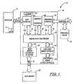
- FIG. 1is a block diagram of a computer system that uses the present invention.
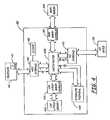
- FIG. 2is a block diagram of the low latency memory controller illustrated in FIG. 1 .
- FIG. 3is a block diagram of another computer system that uses the present invention.
- FIG. 4is a block diagram of yet another computer system that uses the present invention.
- FIG. 1there is shown a computer system 1 comprising an embodiment of the present invention.
- FIG. 1illustrates a computer system 1 comprising a processor 10 , a system controller 50 with an integrated low latency memory 130 , a peripheral device 30 and a main memory 100 .
- the low latency memory 130may be considered a subset of the address space primarily embodied in main memory 100 although within the computer system 1 it is physically distinct from the main memory 100 .
- the low latency memory 130is not intended to mirror any portion of main memory 100 . Instead it represents a unique subset of the main memory. Accordingly, in the present invention, the low latency memory 130 is a unique component of the memory subsystem.
- FIG. 1illustrates a uni-processor computer system, although the present invention may be equally beneficial in multi-processor computer systems.
- the processor 10may be any conventional general purpose single- or multi-chip processor such as a Pentium® Pro processor, a Pentium® processor, a 8051 processor, a MIPS® processor, a Power PC® processor, or an ALPHA® processor.
- the processor 10may be any conventional special purpose processor such as a digital signal processor or a graphics processor.
- the processor 10may have an integrated level one (L1) cache 12 . As shown in FIG. 1, the processor 10 may be operably connected to a host bus 20 . When the processor 10 accesses the memory subsystem (or other portions of the computer system), the processor 10 may be referred to as a requesting agent.
- L1integrated level one
- FIG. 1illustrates a computer system with a single peripheral device 30 , although the present invention may be equally beneficial in computer systems comprising a plurality of peripheral devices.
- the peripheral device 30may be a PCI-based device or an other type of I/O device. As shown in FIG. 1, the peripheral device 30 may be operably connected to a peripheral bus 40 . When the peripheral device 30 accesses the memory subsystem (or other portions of the computer system), the peripheral device 30 may also be referred to as a requesting agent.
- the main memory 100may be one or more conventional memory devices including, without limitation, dynamic random access memories (DRAMs), extended data out DRAMs (EDO DRAMs), burst extended data out DRAMs (BEDO DRAMs), static random access memories (SRAMs), video random access memories (VRAMs), read-only memories (ROMs), electrically erasable programmable read-only memories (EEPROMs), and erasable programmable read-only memories (EPROMs).
- DRAMsdynamic random access memories
- EEO DRAMsextended data out DRAMs
- BEDO DRAMsburst extended data out DRAMs
- SRAMsstatic random access memories
- VRAMsvideo random access memories
- ROMsread-only memories
- EEPROMselectrically erasable programmable read-only memories
- EPROMserasable programmable read-only memories
- the memory devicemay be provided in multi-chip modules (e.g., SIMM or SIP).
- the main memory 100may be cached or cacheable memory; i.e., portions of the data or information stored in the main memory 100 may also be stored in the L1 cache 12 of the processor 10 or in the L2 cache 52 of the system controller 50 . Because the main memory 100 is cacheable, a snoop phase or cycle must be implemented whenever a processor 10 or peripheral device 30 attempts to access a main memory address.
- the main memory 100may be operably connected to the system controller 50 by a main memory bus 92 .
- the system controller 50may also be referred to as system or core logic 50 .
- the system controller 50may be an application specific integrated circuit (ASIC).
- ASICapplication specific integrated circuit
- the system controller 50operates to control the memory subsystem within the computer system (including the main memory 100 and the low latency memory 130 ) in response to memory access requests received by the system controller 50 .
- the system controller 50coordinates the transfer of data to and from the main memory 100 and the low latency memory 130 across the host bus 20 , peripheral bus 40 and memory bus 92 .
- the system controller 50may handle and schedule multiple requests from various buses via bus arbitration control circuitry (not shown).
- the various integrated components of the system controller 50may be operably connected to an internal system controller bus 54 .
- the internal system controller bus 54may have its own proprietary or a standard bus protocol.
- the system controller 50comprises a host interface 60 , a peripheral interface 70 and a request/data multiplexer 80 .
- the system controllermay also comprise an L2 cache 52 .
- the host interface 60may receive data and address information from the processor 10 over the host bus 20 .
- the host interface 60may decode an address received from the processor 10 to determine if the requested address is within main memory 100 or within low latency memory 130 . If the requested address is within the low latency memory 130 , the host interface 60 may assert a select signal (SEL) causing the request/data multiplexer 80 to provide the address request and any data associated with the address request to the low latency memory controller 110 . Otherwise, the address request and any data associated with the address request may be provided to the main memory controller 90 .
- SELselect signal
- the peripheral interface 70may receive data and address information from the peripheral device 30 over the peripheral bus 40 .
- the peripheral interface 70may decode an address received from the peripheral device 30 to determine if the requested address is within main memory 100 or within low latency memory 130 . If the requested address is within the low latency memory 130 , the peripheral interface 70 may assert a select signal (SEL) causing the request/data multiplexer 80 to provide the address request and any data associated with the request to the low latency memory controller 110 . Otherwise, the address request and any data associated with the request may be provided to the main memory controller 90 .
- SELselect signal
- the embedded peripheral 140may be a digital signal processor (DSP) such as a 56000 series DSP manufactured by MotorolaTM. When the embedded peripheral 140 accesses the memory subsystem (or other portions of the computer system), the embedded peripheral may also be referred to as a requesting agent. The embedded peripheral 140 may be utilized to relieve the computational burden on the processor 10 . The embedded peripheral 140 may assert a select signal (SEL) to access the low latency memory 130 . Because all of the data and information required by the embedded peripheral may be stored in low latency memory 130 (that is, the embedded peripheral 140 will have no off chip or other memory space available to it), the select signal line of the embedded peripheral may be hardwired to the low latency memory controller 110 , thereby allowing the embedded peripheral direct access to the low latency memory 130 .
- DSPdigital signal processor
- SELselect signal
- Latency in direct memory accesses to the low latency memory 130is reduced by having the memory on which the embedded peripheral 140 is exclusively dependent on the same “chip” or physical component as the embedded peripheral 140 .
- the embedded peripheral 140 and the low latency memory 130may be on the same system controller ASIC 50 .
- the main memory controller 90generates the control signals necessary to control the main memory 100 in response to main memory access requests provided by the request data multiplexer 80 .
- the main memory controller 90may perform address decoding operations to determine the location in main memory 100 of the access request.
- the low latency memory controller 110generates the control signals necessary to control the low latency memory 130 in response to low latency memory access requests provided by the request data multiplexer 80 . As shown in FIG. 2, the low latency memory controller 110 comprises a request bus controller 114 , a memory sequencer 118 and an optional data buffer 122 .
- the low latency memory 130together with the L2 cache 52 and the main memory 100 comprise the memory subsystem.
- the low latency memory 130may be one or more conventional memory devices including, without limitation, dynamic random access memories (DRAMs), extended data out DRAMs (EDO DRAMs), burst extended data out DRAMs (BEDO DRAMs), static random access memories (SRAMs), video random access memories (VRAMs), read-only memories (ROMs), electrically erasable programmable read-only memories (EEPROMs), and erasable programmable read-only memories (EPROMs).
- DRAMsdynamic random access memories
- EEO DRAMsextended data out DRAMs
- BEDO DRAMsburst extended data out DRAMs
- SRAMsstatic random access memories
- VRAMsvideo random access memories
- ROMsread-only memories
- EEPROMselectrically erasable programmable read-only memories
- EPROMserasable programmable read-only memories
- the low latency memory 130is a subset of the address space primarily embodied in the main memory 100 ; however, the low latency memory 130 is an integral component of the system controller 50 and thus physically distinct from the main memory 100 . Because the low latency memory 130 is an integral component of the system controller 50 (i.e., integrated on the same chip), latency is reduced in accessing the low latency memory 130 as compared to accessing the main memory 100 (which is external to the system controller 50 ). (Generally, transmitting a signal from one chip or computer system component to another results in latency because of the propagation delay involved in transmitting the signal).
- Latencyis further reduced in accessing low latency memory 130 as compared to accessing main memory 100 because, given the relatively smaller size of the low latency memory 130 , address requests to the low latency memory 130 may require fewer clock cycles to decode. Latency may be even further reduced in accessing low latency memory 130 by configuring the low latency memory as noncacheable memory, thus avoiding the need to snoop the L1 cache, L2 cache or low latency memory 130 for data modifications when low latency memory 130 is addressed. Additionally, configuring or manufacturing the low latency memory as SRAM (as compared to main memory DRAM) may also reduce latency.
- FIGS. 3 and 4there are shown alternative embodiments of computer systems comprising the present invention.
- all of the address decoding functionsmay be performed in a host interface 360 .
- access requests issued by a processor 310 or a PCI device 330are provided to the host interface 360 for decoding and accordingly routed to a low latency memory controller 3110 or to so main memory controller 390 .
- all of the address decoding functionsmay be performed in a host interface 460 . In this embodiment, however, all routing of address requests and data associated with address requests is performed by a central switch or router 4200 .
- the low latency memory 3130(FIG. 3) or 4130 (FIG. 4) is integrated on the same chip as the other components of the system controller 350 (FIG. 3) or 450 (FIG. 4 ).
- the low latency benefits afforded by such a configurationare essentially equally available in these embodiments.
- one advantage of the present inventionis an increase in computer system throughput.
- a subseti.e., the low latency memory 130
- this subset of main memory 100is noncacheable
- latency in accessing that subset and average latency of the entire memory subsystemis reduced.
- the number of computer operations or transactions that are interrupted, stalled or have wait states insertedis reduced. This may result in time and cost savings.
- the low latency memory 130is accessible by not only the embedded peripheral 140 , but also the processor 10 and external peripheral 30 .
- the present inventionmay provide particular advantages in the following computer operations or tasks.
- a peripheral devicesuch as a PCI-based device may assert a “busy bit” indicating that the peripheral is performing a transaction.
- This busy bitis typically stored in a noncacheable memory space within the main memory.
- the processor 10must periodically access or poll the address of the busy bit to determine when the peripheral device has completed the transaction.
- each of these repeated accesses to memoryhas inherent latency, thereby reducing computer system throughput.
- the repeated polling of the main memoryincreases main memory bus utilization which effectively reduces the bandwidth of the main memory bus. By storing the busy bit in the low latency memory, the latency in these processor polling operations may be reduced and the main memory bus may be more effectively utilized.
- the busy bit or a similar indication that the peripheral device is performing a transactionmay be stored in the L2 cache.
- This schemeeliminates the need for the processor to access main memory when polling the status of the peripheral.
- a snoop phasemust be implemented which adds latency to the system. By storing the semaphore in the low latency memory, the snoop phase may be eliminated and latency may be reduced.
- bufferingmay be provided at the peripheral for storing data and information while the processor has access to the main memory bus.
- the amount of buffering at the peripheralmust compensate for the inherent latency involved in main memory accesses by the processor. In other words, the more latency inherent in a main memory access, the more buffering that will be required at the peripheral. Thus reducing latency in a subset of main memory accesses, may result in a corresponding reduction in the amount of buffering required at a peripheral.
Landscapes
- Engineering & Computer Science (AREA)
- Theoretical Computer Science (AREA)
- Physics & Mathematics (AREA)
- General Engineering & Computer Science (AREA)
- General Physics & Mathematics (AREA)
- Memory System Of A Hierarchy Structure (AREA)
Abstract
Description
Claims (26)
Priority Applications (1)
| Application Number | Priority Date | Filing Date | Title |
|---|---|---|---|
| US09/994,302US6560680B2 (en) | 1998-01-21 | 2001-11-26 | System controller with Integrated low latency memory using non-cacheable memory physically distinct from main memory |
Applications Claiming Priority (2)
| Application Number | Priority Date | Filing Date | Title |
|---|---|---|---|
| US1025098A | 1998-01-21 | 1998-01-21 | |
| US09/994,302US6560680B2 (en) | 1998-01-21 | 2001-11-26 | System controller with Integrated low latency memory using non-cacheable memory physically distinct from main memory |
Related Parent Applications (1)
| Application Number | Title | Priority Date | Filing Date |
|---|---|---|---|
| US1025098AContinuation | 1998-01-21 | 1998-01-21 |
Publications (2)
| Publication Number | Publication Date |
|---|---|
| US20020099909A1 US20020099909A1 (en) | 2002-07-25 |
| US6560680B2true US6560680B2 (en) | 2003-05-06 |
Family
ID=21744820
Family Applications (1)
| Application Number | Title | Priority Date | Filing Date |
|---|---|---|---|
| US09/994,302Expired - LifetimeUS6560680B2 (en) | 1998-01-21 | 2001-11-26 | System controller with Integrated low latency memory using non-cacheable memory physically distinct from main memory |
Country Status (1)
| Country | Link |
|---|---|
| US (1) | US6560680B2 (en) |
Cited By (10)
| Publication number | Priority date | Publication date | Assignee | Title |
|---|---|---|---|---|
| US20050086417A1 (en)* | 2003-10-17 | 2005-04-21 | Micron Technology, Inc. | Method and apparatus for sending data from multiple sources over a communications bus |
| US20050188121A1 (en)* | 2004-02-19 | 2005-08-25 | Sang-Yeun Cho | System and controller with reduced bus utilization time |
| US20060007201A1 (en)* | 2004-07-06 | 2006-01-12 | Her-Ming Jong | Image display controller with processing data protection |
| US20060059310A1 (en)* | 2004-09-10 | 2006-03-16 | Cavium Networks | Local scratchpad and data caching system |
| US20060271347A1 (en)* | 2002-08-29 | 2006-11-30 | Micron Technology, Inc. | Method for generating commands for testing hardware device models |
| US7558925B2 (en) | 2004-09-10 | 2009-07-07 | Cavium Networks, Inc. | Selective replication of data structures |
| US7594081B2 (en) | 2004-09-10 | 2009-09-22 | Cavium Networks, Inc. | Direct access to low-latency memory |
| US20100191913A1 (en)* | 2009-01-26 | 2010-07-29 | Agere Systems Inc. | Reconfiguration of embedded memory having a multi-level cache |
| WO2015089054A1 (en)* | 2013-12-12 | 2015-06-18 | Samsung Electronics Co., Ltd. | Disaggregated memory appliance |
| US20160117129A1 (en)* | 2013-12-12 | 2016-04-28 | Samsung Electronics Co., Ltd. | Disaggregated memory appliance |
Families Citing this family (11)
| Publication number | Priority date | Publication date | Assignee | Title |
|---|---|---|---|---|
| US20050027940A1 (en)* | 2003-08-01 | 2005-02-03 | Zimmer Vincent J. | Methods and apparatus for migrating a temporary memory location to a main memory location |
| US8560475B2 (en) | 2004-09-10 | 2013-10-15 | Cavium, Inc. | Content search mechanism that uses a deterministic finite automata (DFA) graph, a DFA state machine, and a walker process |
| US8392590B2 (en)* | 2004-09-10 | 2013-03-05 | Cavium, Inc. | Deterministic finite automata (DFA) processing |
| US8301788B2 (en)* | 2004-09-10 | 2012-10-30 | Cavium, Inc. | Deterministic finite automata (DFA) instruction |
| US8819217B2 (en)* | 2007-11-01 | 2014-08-26 | Cavium, Inc. | Intelligent graph walking |
| US8086609B2 (en)* | 2007-11-01 | 2011-12-27 | Cavium, Inc. | Graph caching |
| US7949683B2 (en)* | 2007-11-27 | 2011-05-24 | Cavium Networks, Inc. | Method and apparatus for traversing a compressed deterministic finite automata (DFA) graph |
| US8180803B2 (en)* | 2007-11-27 | 2012-05-15 | Cavium, Inc. | Deterministic finite automata (DFA) graph compression |
| US8473523B2 (en) | 2008-10-31 | 2013-06-25 | Cavium, Inc. | Deterministic finite automata graph traversal with nodal bit mapping |
| US20110016154A1 (en)* | 2009-07-17 | 2011-01-20 | Rajan Goyal | Profile-based and dictionary based graph caching |
| US9612775B1 (en) | 2009-12-30 | 2017-04-04 | Micron Technology, Inc. | Solid state drive controller |
Citations (22)
| Publication number | Priority date | Publication date | Assignee | Title |
|---|---|---|---|---|
| US4797850A (en) | 1986-05-12 | 1989-01-10 | Advanced Micro Devices, Inc. | Dynamic random access memory controller with multiple independent control channels |
| US4903239A (en) | 1987-03-30 | 1990-02-20 | Nec Corporation | Semiconductor memory having a parallel input/output circuit |
| US5161218A (en) | 1989-11-13 | 1992-11-03 | Chips And Technologies, Inc. | Memory controller for using reserved DRAM addresses for EMS |
| US5249160A (en) | 1991-09-05 | 1993-09-28 | Mosel | SRAM with an address and data multiplexer |
| US5317709A (en) | 1990-03-05 | 1994-05-31 | Mitsubishi Denki Kabushiki Kaisha | Microcomputer including memory controller for DRAM |
| US5325504A (en) | 1991-08-30 | 1994-06-28 | Compaq Computer Corporation | Method and apparatus for incorporating cache line replacement and cache write policy information into tag directories in a cache system |
| JPH06348593A (en)* | 1993-06-03 | 1994-12-22 | Sumitomo Electric Ind Ltd | Data transfer controller |
| US5388073A (en) | 1990-04-16 | 1995-02-07 | Hitachi, Ltd. | Semiconductor integrated circuit device and digital processor employing the same |
| US5434969A (en) | 1983-12-30 | 1995-07-18 | Texas Instruments, Incorporated | Video display system using memory with a register arranged to present an entire pixel at once to the display |
| US5477488A (en) | 1994-02-14 | 1995-12-19 | Texas Instruments Incorporated | System, a memory and a process having bit processing circuits associated with memory for pre-processing data read by a processor |
| US5546352A (en) | 1993-12-28 | 1996-08-13 | Mitsubishi Denki Kabushiki Kaisha | Semiconductor memory device having decoder |
| US5583822A (en) | 1994-05-09 | 1996-12-10 | Cirrus Logic, Inc. | Single chip controller-memory device and a memory architecture and methods suitable for implementing the same |
| US5586286A (en) | 1993-03-22 | 1996-12-17 | Compaq Computer Corporation | Memory controller having flip-flops for synchronously generating DRAM address and control signals from a single chip |
| US5602771A (en) | 1988-11-01 | 1997-02-11 | Hitachi, Ltd. | Semiconductor memory device and defect remedying method thereof |
| US5638532A (en) | 1994-12-06 | 1997-06-10 | Digital Equipment Corporation | Apparatus and method for accessing SMRAM in a computer based upon a processor employing system management mode |
| US5659715A (en) | 1993-11-30 | 1997-08-19 | Vlsi Technology, Inc. | Method and apparatus for allocating display memory and main memory employing access request arbitration and buffer control |
| US5704058A (en)* | 1995-04-21 | 1997-12-30 | Derrick; John E. | Cache bus snoop protocol for optimized multiprocessor computer system |
| US5818464A (en) | 1995-08-17 | 1998-10-06 | Intel Corporation | Method and apparatus for arbitrating access requests to a shared computer system memory by a graphics controller and memory controller |
| US5909696A (en) | 1996-06-04 | 1999-06-01 | Intel Corporation | Method and apparatus for caching system management mode information with other information |
| US6003120A (en) | 1993-12-30 | 1999-12-14 | Intel Corporation | Method and apparatus for performing variable length processor write cycles |
| US6018792A (en)* | 1997-07-02 | 2000-01-25 | Micron Electronics, Inc. | Apparatus for performing a low latency memory read with concurrent snoop |
| US6178481B1 (en) | 1995-12-18 | 2001-01-23 | Texas Instruments Incorporated | Microprocessor circuits and systems with life spanned storage circuit for storing non-cacheable data |
- 2001
- 2001-11-26USUS09/994,302patent/US6560680B2/ennot_activeExpired - Lifetime
Patent Citations (22)
| Publication number | Priority date | Publication date | Assignee | Title |
|---|---|---|---|---|
| US5434969A (en) | 1983-12-30 | 1995-07-18 | Texas Instruments, Incorporated | Video display system using memory with a register arranged to present an entire pixel at once to the display |
| US4797850A (en) | 1986-05-12 | 1989-01-10 | Advanced Micro Devices, Inc. | Dynamic random access memory controller with multiple independent control channels |
| US4903239A (en) | 1987-03-30 | 1990-02-20 | Nec Corporation | Semiconductor memory having a parallel input/output circuit |
| US5602771A (en) | 1988-11-01 | 1997-02-11 | Hitachi, Ltd. | Semiconductor memory device and defect remedying method thereof |
| US5161218A (en) | 1989-11-13 | 1992-11-03 | Chips And Technologies, Inc. | Memory controller for using reserved DRAM addresses for EMS |
| US5317709A (en) | 1990-03-05 | 1994-05-31 | Mitsubishi Denki Kabushiki Kaisha | Microcomputer including memory controller for DRAM |
| US5388073A (en) | 1990-04-16 | 1995-02-07 | Hitachi, Ltd. | Semiconductor integrated circuit device and digital processor employing the same |
| US5325504A (en) | 1991-08-30 | 1994-06-28 | Compaq Computer Corporation | Method and apparatus for incorporating cache line replacement and cache write policy information into tag directories in a cache system |
| US5249160A (en) | 1991-09-05 | 1993-09-28 | Mosel | SRAM with an address and data multiplexer |
| US5586286A (en) | 1993-03-22 | 1996-12-17 | Compaq Computer Corporation | Memory controller having flip-flops for synchronously generating DRAM address and control signals from a single chip |
| JPH06348593A (en)* | 1993-06-03 | 1994-12-22 | Sumitomo Electric Ind Ltd | Data transfer controller |
| US5659715A (en) | 1993-11-30 | 1997-08-19 | Vlsi Technology, Inc. | Method and apparatus for allocating display memory and main memory employing access request arbitration and buffer control |
| US5546352A (en) | 1993-12-28 | 1996-08-13 | Mitsubishi Denki Kabushiki Kaisha | Semiconductor memory device having decoder |
| US6003120A (en) | 1993-12-30 | 1999-12-14 | Intel Corporation | Method and apparatus for performing variable length processor write cycles |
| US5477488A (en) | 1994-02-14 | 1995-12-19 | Texas Instruments Incorporated | System, a memory and a process having bit processing circuits associated with memory for pre-processing data read by a processor |
| US5583822A (en) | 1994-05-09 | 1996-12-10 | Cirrus Logic, Inc. | Single chip controller-memory device and a memory architecture and methods suitable for implementing the same |
| US5638532A (en) | 1994-12-06 | 1997-06-10 | Digital Equipment Corporation | Apparatus and method for accessing SMRAM in a computer based upon a processor employing system management mode |
| US5704058A (en)* | 1995-04-21 | 1997-12-30 | Derrick; John E. | Cache bus snoop protocol for optimized multiprocessor computer system |
| US5818464A (en) | 1995-08-17 | 1998-10-06 | Intel Corporation | Method and apparatus for arbitrating access requests to a shared computer system memory by a graphics controller and memory controller |
| US6178481B1 (en) | 1995-12-18 | 2001-01-23 | Texas Instruments Incorporated | Microprocessor circuits and systems with life spanned storage circuit for storing non-cacheable data |
| US5909696A (en) | 1996-06-04 | 1999-06-01 | Intel Corporation | Method and apparatus for caching system management mode information with other information |
| US6018792A (en)* | 1997-07-02 | 2000-01-25 | Micron Electronics, Inc. | Apparatus for performing a low latency memory read with concurrent snoop |
Cited By (21)
| Publication number | Priority date | Publication date | Assignee | Title |
|---|---|---|---|---|
| US20060271347A1 (en)* | 2002-08-29 | 2006-11-30 | Micron Technology, Inc. | Method for generating commands for testing hardware device models |
| US7779212B2 (en) | 2003-10-17 | 2010-08-17 | Micron Technology, Inc. | Method and apparatus for sending data from multiple sources over a communications bus |
| US20050086417A1 (en)* | 2003-10-17 | 2005-04-21 | Micron Technology, Inc. | Method and apparatus for sending data from multiple sources over a communications bus |
| US9652412B2 (en) | 2003-10-17 | 2017-05-16 | Micron Technology, Inc. | Method and apparatus for sending data from multiple sources over a communications bus |
| US8806152B2 (en) | 2003-10-17 | 2014-08-12 | Micron Technology, Inc. | Method and apparatus for sending data from multiple sources over a communications bus |
| US8327089B2 (en) | 2003-10-17 | 2012-12-04 | Micron Technology, Inc. | Method and apparatus for sending data from multiple sources over a communications bus |
| US20100299440A1 (en)* | 2003-10-17 | 2010-11-25 | Meyer James W | Method and apparatus for sending data from multiple sources over a communications bus |
| US8095748B2 (en) | 2003-10-17 | 2012-01-10 | Micron Technology, Inc. | Method and apparatus for sending data from multiple sources over a communications bus |
| US7543114B2 (en)* | 2004-02-19 | 2009-06-02 | Samsung Electronics Co., Ltd. | System and controller with reduced bus utilization time |
| US20050188121A1 (en)* | 2004-02-19 | 2005-08-25 | Sang-Yeun Cho | System and controller with reduced bus utilization time |
| US20060007201A1 (en)* | 2004-07-06 | 2006-01-12 | Her-Ming Jong | Image display controller with processing data protection |
| US7594081B2 (en) | 2004-09-10 | 2009-09-22 | Cavium Networks, Inc. | Direct access to low-latency memory |
| US7558925B2 (en) | 2004-09-10 | 2009-07-07 | Cavium Networks, Inc. | Selective replication of data structures |
| US7941585B2 (en) | 2004-09-10 | 2011-05-10 | Cavium Networks, Inc. | Local scratchpad and data caching system |
| US20060059316A1 (en)* | 2004-09-10 | 2006-03-16 | Cavium Networks | Method and apparatus for managing write back cache |
| US9141548B2 (en) | 2004-09-10 | 2015-09-22 | Cavium, Inc. | Method and apparatus for managing write back cache |
| US20060059310A1 (en)* | 2004-09-10 | 2006-03-16 | Cavium Networks | Local scratchpad and data caching system |
| US20100191913A1 (en)* | 2009-01-26 | 2010-07-29 | Agere Systems Inc. | Reconfiguration of embedded memory having a multi-level cache |
| WO2015089054A1 (en)* | 2013-12-12 | 2015-06-18 | Samsung Electronics Co., Ltd. | Disaggregated memory appliance |
| US20160117129A1 (en)* | 2013-12-12 | 2016-04-28 | Samsung Electronics Co., Ltd. | Disaggregated memory appliance |
| US10254987B2 (en)* | 2013-12-12 | 2019-04-09 | Samsung Electronics Co., Ltd. | Disaggregated memory appliance having a management processor that accepts request from a plurality of hosts for management, configuration and provisioning of memory |
Also Published As
| Publication number | Publication date |
|---|---|
| US20020099909A1 (en) | 2002-07-25 |
Similar Documents
| Publication | Publication Date | Title |
|---|---|---|
| US6560680B2 (en) | System controller with Integrated low latency memory using non-cacheable memory physically distinct from main memory | |
| US6222564B1 (en) | Method and apparatus for managing access to a computer system memory shared by a graphics controller and a memory controller | |
| US9405696B2 (en) | Cache and method for cache bypass functionality | |
| US5404464A (en) | Bus control system and method that selectively generate an early address strobe | |
| EP0434250B1 (en) | Apparatus and method for reducing interference in two-level cache memories | |
| US5404489A (en) | System and method for minimizing cache interruptions by inhibiting snoop cycles if access is to an exclusive page | |
| US5813022A (en) | Circuit for placing a cache memory into low power mode in response to special bus cycles executed on the bus | |
| US6330645B1 (en) | Multi-stream coherent memory controller apparatus and method | |
| US5623632A (en) | System and method for improving multilevel cache performance in a multiprocessing system | |
| US6789169B2 (en) | Embedded DRAM cache memory and method having reduced latency | |
| US6321296B1 (en) | SDRAM L3 cache using speculative loads with command aborts to lower latency | |
| US6918012B2 (en) | Streamlined cache coherency protocol system and method for a multiple processor single chip device | |
| US5561779A (en) | Processor board having a second level writeback cache system and a third level writethrough cache system which stores exclusive state information for use in a multiprocessor computer system | |
| US5522057A (en) | Hybrid write back/write through cache having a streamlined four state cache coherency protocol for uniprocessor computer systems | |
| US8359414B2 (en) | Retry mechanism | |
| EP0301354A2 (en) | Cache consistency protocol for multiprocessor system | |
| MX2007015246A (en) | Method and apparatus for managing cache memory accesses. | |
| US5829027A (en) | Removable processor board having first, second and third level cache system for use in a multiprocessor computer system | |
| US5987544A (en) | System interface protocol with optional module cache | |
| US5765195A (en) | Method for distributing interprocessor interrupt requests via cache memory coherency mechanisms | |
| JPH11272552A (en) | Bridge method, bus bridge, and multiprocessor system | |
| US6789168B2 (en) | Embedded DRAM cache | |
| US5717894A (en) | Method and apparatus for reducing write cycle wait states in a non-zero wait state cache system | |
| US6397299B1 (en) | Reduced latency memory configuration method using non-cacheable memory physically distinct from main memory | |
| EP0681241A1 (en) | Processor board having a second level writeback cache system and a third level writethrough cache system which stores exclusive state information for use in a multiprocessor computer system |
Legal Events
| Date | Code | Title | Description |
|---|---|---|---|
| STCF | Information on status: patent grant | Free format text:PATENTED CASE | |
| CC | Certificate of correction | ||
| FPAY | Fee payment | Year of fee payment:4 | |
| FPAY | Fee payment | Year of fee payment:8 | |
| FPAY | Fee payment | Year of fee payment:12 | |
| AS | Assignment | Owner name:U.S. BANK NATIONAL ASSOCIATION, AS COLLATERAL AGENT, CALIFORNIA Free format text:SECURITY INTEREST;ASSIGNOR:MICRON TECHNOLOGY, INC.;REEL/FRAME:038669/0001 Effective date:20160426 Owner name:U.S. BANK NATIONAL ASSOCIATION, AS COLLATERAL AGEN Free format text:SECURITY INTEREST;ASSIGNOR:MICRON TECHNOLOGY, INC.;REEL/FRAME:038669/0001 Effective date:20160426 | |
| AS | Assignment | Owner name:MORGAN STANLEY SENIOR FUNDING, INC., AS COLLATERAL AGENT, MARYLAND Free format text:PATENT SECURITY AGREEMENT;ASSIGNOR:MICRON TECHNOLOGY, INC.;REEL/FRAME:038954/0001 Effective date:20160426 Owner name:MORGAN STANLEY SENIOR FUNDING, INC., AS COLLATERAL Free format text:PATENT SECURITY AGREEMENT;ASSIGNOR:MICRON TECHNOLOGY, INC.;REEL/FRAME:038954/0001 Effective date:20160426 | |
| AS | Assignment | Owner name:U.S. BANK NATIONAL ASSOCIATION, AS COLLATERAL AGENT, CALIFORNIA Free format text:CORRECTIVE ASSIGNMENT TO CORRECT THE REPLACE ERRONEOUSLY FILED PATENT #7358718 WITH THE CORRECT PATENT #7358178 PREVIOUSLY RECORDED ON REEL 038669 FRAME 0001. ASSIGNOR(S) HEREBY CONFIRMS THE SECURITY INTEREST;ASSIGNOR:MICRON TECHNOLOGY, INC.;REEL/FRAME:043079/0001 Effective date:20160426 Owner name:U.S. BANK NATIONAL ASSOCIATION, AS COLLATERAL AGEN Free format text:CORRECTIVE ASSIGNMENT TO CORRECT THE REPLACE ERRONEOUSLY FILED PATENT #7358718 WITH THE CORRECT PATENT #7358178 PREVIOUSLY RECORDED ON REEL 038669 FRAME 0001. ASSIGNOR(S) HEREBY CONFIRMS THE SECURITY INTEREST;ASSIGNOR:MICRON TECHNOLOGY, INC.;REEL/FRAME:043079/0001 Effective date:20160426 | |
| AS | Assignment | Owner name:MICRON TECHNOLOGY, INC., IDAHO Free format text:RELEASE BY SECURED PARTY;ASSIGNOR:U.S. BANK NATIONAL ASSOCIATION, AS COLLATERAL AGENT;REEL/FRAME:047243/0001 Effective date:20180629 | |
| AS | Assignment | Owner name:MICRON TECHNOLOGY, INC., IDAHO Free format text:RELEASE BY SECURED PARTY;ASSIGNOR:MORGAN STANLEY SENIOR FUNDING, INC., AS COLLATERAL AGENT;REEL/FRAME:050937/0001 Effective date:20190731 |